WO2011096175A1 - Digital amplifier - Google Patents
Digital amplifier Download PDFInfo
- Publication number
- WO2011096175A1 WO2011096175A1 PCT/JP2011/000428 JP2011000428W WO2011096175A1 WO 2011096175 A1 WO2011096175 A1 WO 2011096175A1 JP 2011000428 W JP2011000428 W JP 2011000428W WO 2011096175 A1 WO2011096175 A1 WO 2011096175A1
- Authority
- WO
- WIPO (PCT)
- Prior art keywords
- voltage
- bootstrap capacitor
- bootstrap
- amplifier
- circuit
- Prior art date
Links
Images

Classifications
-
- H—ELECTRICITY
- H03—ELECTRONIC CIRCUITRY
- H03K—PULSE TECHNIQUE
- H03K17/00—Electronic switching or gating, i.e. not by contact-making and –breaking
- H03K17/51—Electronic switching or gating, i.e. not by contact-making and –breaking characterised by the components used
- H03K17/56—Electronic switching or gating, i.e. not by contact-making and –breaking characterised by the components used by the use, as active elements, of semiconductor devices
- H03K17/687—Electronic switching or gating, i.e. not by contact-making and –breaking characterised by the components used by the use, as active elements, of semiconductor devices the devices being field-effect transistors
- H03K17/6871—Electronic switching or gating, i.e. not by contact-making and –breaking characterised by the components used by the use, as active elements, of semiconductor devices the devices being field-effect transistors the output circuit comprising more than one controlled field-effect transistor
-
- H—ELECTRICITY
- H03—ELECTRONIC CIRCUITRY
- H03F—AMPLIFIERS
- H03F3/00—Amplifiers with only discharge tubes or only semiconductor devices as amplifying elements
- H03F3/20—Power amplifiers, e.g. Class B amplifiers, Class C amplifiers
- H03F3/21—Power amplifiers, e.g. Class B amplifiers, Class C amplifiers with semiconductor devices only
- H03F3/217—Class D power amplifiers; Switching amplifiers
-
- H—ELECTRICITY
- H03—ELECTRONIC CIRCUITRY
- H03K—PULSE TECHNIQUE
- H03K2217/00—Indexing scheme related to electronic switching or gating, i.e. not by contact-making or -breaking covered by H03K17/00
- H03K2217/0081—Power supply means, e.g. to the switch driver
Definitions
- the present invention relates to a digital amplifier that charges a bootstrap capacitor at startup.
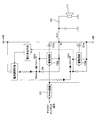
- FIG. 3 is a circuit diagram showing the configuration of the output stage of the class D amplifier.
- an analog audio signal is converted into a digital pulse signal by a PWM (Pulse WidthulationModulation) circuit 101.
- the digital pulse signal is amplified by an amplification circuit 103 having FETs 131a and 131b and drive circuits 133a and 133b each formed in two upper and lower stages, and then decoded into an analog signal by a demodulation circuit 107 formed by an LC circuit.
- the class D amplifier is provided with a bootstrap capacitor Cb for bootstrapping the power supplied to the drive circuit 133b for the upper FET 131b.
- the amplification circuit 103 amplifies the digital pulse signal by alternately turning on and off the upper and lower two-stage FETs 131a and 131b.
- the output of the amplifier circuit 103 becomes ⁇ Vb and is stored in the bootstrap capacitor Cb.
- the low-side FET 131a is turned off and the high-side FET 131b is turned on, power supplied with the voltage of the bootstrap capacitor Cb is supplied to the high-side drive circuit 133b.
- Patent Document 1 discloses a driver having a precharge circuit including a bootstrap circuit that precharges a bootstrap capacitor before startup or before transferring a signal from an oscillator.
- the timing circuit supplies a precharge timing signal for controlling the precharge circuit to supply power to the high side driver before the high side driver receives the drive signal.
- An object of the present invention is to provide a digital amplifier that can reliably charge the bootstrap capacitor with simple control during startup.
- the digital amplifier of the present invention drives a digital pulse signal conversion unit that converts an analog signal into a digital pulse signal, two switching units connected in series, and a power supply of a predetermined voltage to drive one of the two switching units.
- the bootstrap control unit is configured to charge the bootstrap capacitor if a boot voltage obtained by adding the output voltage of the bootstrap capacitor to the predetermined voltage is less than a predetermined value. is doing. With this configuration, the bootstrap capacitor can be reliably charged with simple control.
- the bootstrap control unit includes a monitoring unit that monitors the boot voltage with respect to the output voltage of the amplification unit, and sets a current path to the bootstrap capacitor in accordance with the boot voltage. It has a structure that opens and closes. With this configuration, when the AC power supply is temporarily reduced or the digital amplifier is operating at full power, the bootstrap capacitor can be automatically recharged even if the boot voltage is reduced. In addition, when charging of the bootstrap capacitor is completed, the charging can be stopped, so that power consumption can be reduced.
- the monitoring unit is, for example, the Zener diode Dz in the embodiment.
- the bootstrap capacitor can be reliably charged by simple control at the time of startup.
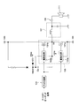
- FIG. 1 is a circuit diagram showing a configuration of a digital amplifier according to an embodiment of the present invention.
- Circuit diagram showing configuration of output stage of class D amplifier The circuit diagram which shows the structure of the digital amplifier of other embodiment which concerns on this invention.
- FIG. 1 is a circuit diagram showing a configuration of an output stage of a digital amplifier according to an embodiment of the present invention.
- the digital amplifier shown in FIG. 1 is a class D amplifier, and includes a PWM (Pulse Width Modulation) circuit 101, an amplifier circuit 103, a bootstrap capacitor Cb, a bootstrap control circuit 105, and a demodulation circuit 107.
- the digital amplifier of this embodiment is different from the class D amplifier shown in FIG. 3 in that a bootstrap control circuit 105 is provided.
- a speaker 111 is connected as a load to the output terminal 109 of the digital amplifier.
- each component provided in the digital amplifier of this embodiment will be described.
- the PWM circuit 101 performs pulse width modulation on an analog audio signal collected by a microphone (not shown) or an analog audio signal from various sound source sources and converts it into a digital pulse signal.
- the amplification circuit 103 includes FETs 131a and 131b connected in series in two upper and lower stages, and drive circuits 133a and 133b for driving the FETs.
- the lower (low side) drive circuit 133a controls switching of the low side FET 131a
- the upper (high side) drive circuit 133b controls switching of the high side FET 131b.
- the amplifier circuit 103 amplifies the digital pulse signal output from the PWM circuit 101 by alternately turning on and off these two upper and lower FETs 131a and 131b.
- the positive power supply Vcc (+ Vcc) is supplied to the drive circuit 133a on the low side.
- the positive power supply Vcc is a voltage required for the drive circuit 133a to turn on the FET 131a, and is, for example, “ ⁇ Vb + ⁇ ” (V).
- ⁇ Vb is a negative power supply voltage
- ⁇ is, for example, +5 to +10 (V).
- the power supply of the boot voltage Vboot obtained by adding the output voltage of the bootstrap capacitor Cb to the positive power supply Vb (+ Vb) is supplied to the drive circuit 133b on the high side.
- the high-side FET 131b is turned on when the boot voltage Vboot is equal to or higher than “+ Vb + ⁇ ” (V).
- the bootstrap capacitor Cb is a capacitor for bootstrapping the power supplied to the drive circuit 133b on the high side. Note that one end of the bootstrap capacitor Cb is connected to the drive circuit 133 b on the high side, and the other end is connected to the output of the amplifier circuit 103.
- the bootstrap control circuit 105 includes a resistor R1, a Zener diode Dz, Darlington-connected transistors Tr1 and Tr2, a diode D1, and a resistor R2.
- the resistor R1 and the Zener diode Dz are connected in series between the positive power source of the power source voltage (+ Vb) and the output of the amplifier circuit 103.
- the resistor R2, Darlington-connected transistors Tr1 and Tr2, and the diode D1 are connected in series between the positive power supply of the power supply voltage (+ Vb) and the bootstrap capacitor Cb. Further, as shown in FIG. 1, the cathode of the Zener diode Dz is connected to the base of the first-stage transistor Tr1.
- the operation of the bootstrap control circuit 105 when the digital amplifier according to this embodiment is started will be described.
- the digital amplifier according to this embodiment is activated, when the low-side FET 131a is turned on, the output voltage Vo of the amplifier circuit 103 is ⁇ Vb.
- the bootstrap capacitor Cb is charged until the boot voltage Vboot reaches the threshold value “Vz ⁇ 2Vbe ⁇ Vf” (at this time, the positive power supply ( (+ Vcc) is not sufficiently high, so the bootstrap capacitor Cb is not charged from the positive power supply (+ Vcc).
- Vz is a voltage on the cathode side of the Zener diode Dz, and is a voltage that is dropped from the positive power supply voltage (+ Vb) by the resistor R1.
- Vbe is the base-emitter voltage of the transistors Tr1 and Tr2.
- Vf is a forward voltage of the diode D1. Further, the charging current of the bootstrap capacitor Cb depends on the resistance value of the resistor R2.
- the bootstrap capacitor Cb When the positive power supply (+ Vcc) reaches a sufficiently high voltage, the bootstrap capacitor Cb is charged from the positive power supply (+ Vcc), and when the boot voltage Vboot reaches the threshold value “Vz ⁇ 2Vbe ⁇ Vf”, a Darlington connection is established.
- the transistors Tr1 and Tr2 are turned off when the base-emitter voltage becomes Vbe or less, and the current path from the positive power supply of the power supply voltage (+ Vb) to the bootstrap capacitor Cb is cut off.
- the boot voltage Vboot reaches the threshold value “Vz ⁇ 2Vbe ⁇ Vf”
- the charging of the bootstrap capacitor Cb is stopped.
- the digital amplifier according to this embodiment when the digital amplifier according to this embodiment is activated, when the high-side FET 131b is turned on, the output voltage of the bootstrap capacitor Cb is not sufficient, and the boot voltage Vboot is less than “+ Vb + ⁇ ” (V).
- the high-side drive circuit 133b cannot drive the FET 131b on.
- the two FETs 131a and 131b are both in the off state, and the output voltage Vo of the amplifier circuit 103 becomes a value close to 0 (V). Therefore, the bootstrap capacitor Cb is charged because it does not satisfy “Vz ⁇ 2Vbe ⁇ Vf”.
- the demodulating circuit 107 is composed of an LC circuit, and demodulates the digital pulse signal amplified by the amplifying circuit 103 and converts it into an analog audio signal.
- the analog audio signal converted by the demodulation circuit 107 is output from the speaker 111 via the output terminal 109.
- the bootstrap capacitor Cb is immediately after startup even when the digital amplifier is started up, even when the high-side FET 131b of the amplifier circuit 103 is turned on. Since the battery is charged, the high-side drive circuit 133b can turn on the FET 131b.
- This function is realized by the bootstrap control circuit 105.
- the control performed by the bootstrap control circuit 105 is charged according to the storage state of the bootstrap capacitor Cb, whether it is on-driven from the high-side FET 131b or the low-side FET 131a. It's as simple as doing.
- the digital amplifier when the digital amplifier is activated, the bootstrap capacitor can be reliably charged by simple control. As a result, the digital amplifier is reliably activated.
- the bootstrap control circuit 105 stops charging. Therefore, the power consumption of the digital amplifier can be reduced.
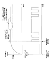
- the boot voltage Vboot is lowered as shown in FIG.
- the bootstrap control circuit 105 charges the bootstrap capacitor Cb again. The output voltage of the bootstrap capacitor Cb charged in this way can compensate for the decrease in the boot voltage Vboot.
- the amplifier circuit 103 includes the FETs 131a and 131b configured in two upper and lower stages, but may be a bipolar transistor or an IGBT.
- the bootstrap capacitor Cb and the bootstrap control circuit 105 are provided for the drive circuit 133b on the high side, but similar means may be provided on the low side as shown in FIG. .
- the voltage detection means (corresponding to the Zener diode Dz) shown in FIG. 4 may detect the voltage supplied to the low-side drive circuit 133a, as indicated by the dotted line.
- the digital amplifier is described as including the PWM circuit 101 and the demodulation circuit 107. However, these may be configured as a unit separate from the digital amplifier.
- the present invention is useful as a digital amplifier or the like that charges a bootstrap capacitor at startup.
Abstract
Disclosed is a digital amplifier provided with an amplifier unit, a bootstrap capacitor, and a bootstrap control unit. The amplifier unit comprises two serially connected switching units, a first drive unit that activates by way of a supply of power of a predetermined voltage to drive one of the switching units, and a second drive unit that actives by way of a supply of power of higher voltage than the predetermined voltage to drive the other switching unit; wherein digital pulse signals are amplified by alternating the two switching units between on and off states. The bootstrap capacitor bootstraps a power supply for supplying the second drive unit. The bootstrap control unit controls charging of the bootstrap capacitor. The bootstrap control unit performs charging of the bootstrap capacitor if a boot voltage, which is the output voltage of the bootstrap capacitor added to the predetermined voltage, is less than a predetermined value. Therefore, it is possible to provide a digital amplifier for reliably performing charging of the bootstrap capacitor at startup time by way of simple control.
Description
本発明は、起動時にブートストラップコンデンサを充電するデジタルアンプに関する。
The present invention relates to a digital amplifier that charges a bootstrap capacitor at startup.
D級アンプの出力段は、NchのMOSFET(以下、単に「FET」という)を上下2段に組み合わせて構成されている。図3は、D級アンプの出力段の構成を示す回路図である。図3に示すように、D級アンプでは、PWM(Pulse Width Modulation)回路101によって、例えばアナログオーディオ信号がデジタルパルス信号に変換される。デジタルパルス信号は、それぞれ上下2段に構成されたFET131a,131b及び駆動回路133a,133bを有する増幅回路103によって増幅された後、LC回路で構成された復調回路107によってアナログ信号に復号される。なお、当該D級アンプには、上段のFET131b用の駆動回路133bに供給する電源をブートストラップするためのブートストラップコンデンサCbが設けられている。
The output stage of the class D amplifier is configured by combining Nch MOSFETs (hereinafter simply referred to as “FETs”) in two upper and lower stages. FIG. 3 is a circuit diagram showing the configuration of the output stage of the class D amplifier. As shown in FIG. 3, in the class D amplifier, for example, an analog audio signal is converted into a digital pulse signal by a PWM (Pulse WidthulationModulation) circuit 101. The digital pulse signal is amplified by an amplification circuit 103 having FETs 131a and 131b and drive circuits 133a and 133b each formed in two upper and lower stages, and then decoded into an analog signal by a demodulation circuit 107 formed by an LC circuit. The class D amplifier is provided with a bootstrap capacitor Cb for bootstrapping the power supplied to the drive circuit 133b for the upper FET 131b.
増幅回路103は、上下2段のFET131a,131bを交互にオンオフすることによってデジタルパルス信号を増幅する。まず、下段(ローサイド側)のFET131aがオンして、上段(ハイサイド側)のFET131bがオフすると、増幅回路103の出力は-Vbとなり、ブートストラップコンデンサCbに蓄電される。次に、ローサイド側のFET131aがオフして、ハイサイド側のFET131bがオンする際には、ブートストラップコンデンサCbの電圧が加わった電源がハイサイド側の駆動回路133bに供給される。
The amplification circuit 103 amplifies the digital pulse signal by alternately turning on and off the upper and lower two- stage FETs 131a and 131b. First, when the lower (low-side) FET 131a is turned on and the upper (high-side) FET 131b is turned off, the output of the amplifier circuit 103 becomes −Vb and is stored in the bootstrap capacitor Cb. Next, when the low-side FET 131a is turned off and the high-side FET 131b is turned on, power supplied with the voltage of the bootstrap capacitor Cb is supplied to the high-side drive circuit 133b.
このように、ハイサイド側のFET131bを駆動する際には、駆動回路133bに供給する電源をブートストラップする必要がある。したがって、予めブートストラップコンデンサCbを充電するために、ローサイド側のFET131aからオンする必要がある。すなわち、当該D級アンプの起動時には、ローサイド側のFET131aからオンする必要がある。
Thus, when driving the high-side FET 131b, it is necessary to bootstrap the power supplied to the drive circuit 133b. Therefore, it is necessary to turn on the FET 131a on the low side in order to charge the bootstrap capacitor Cb in advance. In other words, when starting up the class D amplifier, it is necessary to turn it on from the FET 131a on the low side.
特許文献1には、スタートアップ前又は発振器から信号を転送する前にブートストラップコンデンサをプリチャージするブートストラップ回路を含むプリチャージ回路を有するドライバが開示されている。当該ドライバでは、タイミング回路が、ハイ側ドライバがドライブ信号を受け取る前にハイ側ドライバに給電するため、プリチャージ回路を制御するプリチャージタイミング信号を供給している。
Patent Document 1 discloses a driver having a precharge circuit including a bootstrap circuit that precharges a bootstrap capacitor before startup or before transferring a signal from an oscillator. In the driver, the timing circuit supplies a precharge timing signal for controlling the precharge circuit to supply power to the high side driver before the high side driver receives the drive signal.
上記説明した特許文献1のドライバにはタイミング回路が必要であり、かつ、プリチャージ回路の制御シーケンスが複雑である。
The driver described in Patent Document 1 described above requires a timing circuit, and the control sequence of the precharge circuit is complicated.
本発明の目的は、起動時にブートストラップコンデンサの充電を簡単な制御で確実に行うことができるデジタルアンプを提供することである。
An object of the present invention is to provide a digital amplifier that can reliably charge the bootstrap capacitor with simple control during startup.
本発明のデジタルアンプは、アナログ信号をデジタルパルス信号に変換するデジタルパルス信号変換部と、直列接続された2つのスイッチング部、所定電圧の電源供給によって動作して前記2つのスイッチング部の一方を駆動する第1の駆動部、および前記所定電圧より高い電圧の電源供給によって動作して前記2つのスイッチング部の他方を駆動する第2の駆動部を有し、前記2つのスイッチング部を交互にオンオフすることによって前記デジタルパルス信号を増幅する増幅部と、前記第2の駆動部に供給する電源をブートストラップするブートストラップコンデンサと、前記ブートストラップコンデンサの充電を制御するブートストラップ制御部と、前記増幅部によって増幅されたデジタルパルス信号をアナログ信号に変換するアナログ信号変換部と、を備え、前記ブートストラップ制御部は、前記所定電圧に前記ブートストラップコンデンサの出力電圧を加えたブート電圧が所定値未満であれば、前記ブートストラップコンデンサの充電を行う構成を有している。
この構成により、ブートストラップコンデンサの充電を簡単な制御で確実に行うことができる。 The digital amplifier of the present invention drives a digital pulse signal conversion unit that converts an analog signal into a digital pulse signal, two switching units connected in series, and a power supply of a predetermined voltage to drive one of the two switching units. A first drive unit that operates and a second drive unit that operates by power supply of a voltage higher than the predetermined voltage to drive the other of the two switching units, and alternately turns on and off the two switching units. An amplifier for amplifying the digital pulse signal, a bootstrap capacitor for bootstrapping the power supplied to the second driver, a bootstrap controller for controlling charging of the bootstrap capacitor, and the amplifier Analog that converts the digital pulse signal amplified by the analog signal The bootstrap control unit is configured to charge the bootstrap capacitor if a boot voltage obtained by adding the output voltage of the bootstrap capacitor to the predetermined voltage is less than a predetermined value. is doing.
With this configuration, the bootstrap capacitor can be reliably charged with simple control.
また、本発明のデジタルアンプにおいて、前記ブートストラップ制御部は、前記増幅部の出力電圧に対する前記ブート電圧を監視する監視部を有し、前記ブート電圧に応じて前記ブートストラップコンデンサへの電流経路を開閉する構成を有している。
この構成により、AC電源が一時的に低下したとき又はデジタルアンプがフルパワーで動作しているときに、ブート電圧が低下しても、ブートストラップコンデンサの再充電を自動で行うことができる。また、ブートストラップコンデンサへの充電が完了すれば、充電を停止できるため消費電力の低減も可能となる。なお、監視部は、例えば、実施の形態でのツェナーダイオードDzである。 In the digital amplifier of the present invention, the bootstrap control unit includes a monitoring unit that monitors the boot voltage with respect to the output voltage of the amplification unit, and sets a current path to the bootstrap capacitor in accordance with the boot voltage. It has a structure that opens and closes.
With this configuration, when the AC power supply is temporarily reduced or the digital amplifier is operating at full power, the bootstrap capacitor can be automatically recharged even if the boot voltage is reduced. In addition, when charging of the bootstrap capacitor is completed, the charging can be stopped, so that power consumption can be reduced. The monitoring unit is, for example, the Zener diode Dz in the embodiment.
本発明に係るデジタルアンプによれば、起動時にブートストラップコンデンサの充電を簡単な制御で確実に行うことができる。
According to the digital amplifier of the present invention, the bootstrap capacitor can be reliably charged by simple control at the time of startup.
以下、本発明の実施形態について、図面を参照して説明する。
Hereinafter, embodiments of the present invention will be described with reference to the drawings.
図1は、本発明に係る一実施形態のデジタルアンプの出力段の構成を示す回路図である。なお、図1では、図3と共通する構成要素には同じ参照符号が付されている。図1に示すデジタルアンプは、D級アンプであって、PWM(Pulse Width Modulation)回路101と、増幅回路103と、ブートストラップコンデンサCbと、ブートストラップ制御回路105と、復調回路107とを備える。本実施形態のデジタルアンプが図3に示したD級アンプと異なる点は、ブートストラップ制御回路105を備えたことである。なお、図1では、負荷としてスピーカ111がデジタルアンプの出力端109に接続されている。以下、本実施形態のデジタルアンプが備える各構成要素について説明する。
FIG. 1 is a circuit diagram showing a configuration of an output stage of a digital amplifier according to an embodiment of the present invention. In FIG. 1, the same reference numerals are assigned to components common to FIG. 3. The digital amplifier shown in FIG. 1 is a class D amplifier, and includes a PWM (Pulse Width Modulation) circuit 101, an amplifier circuit 103, a bootstrap capacitor Cb, a bootstrap control circuit 105, and a demodulation circuit 107. The digital amplifier of this embodiment is different from the class D amplifier shown in FIG. 3 in that a bootstrap control circuit 105 is provided. In FIG. 1, a speaker 111 is connected as a load to the output terminal 109 of the digital amplifier. Hereinafter, each component provided in the digital amplifier of this embodiment will be described.
PWM回路101は、図示しないマイクロフォンにより集音されたアナログオーディオ信号又は各種音源ソースからのアナログオーディオ信号をパルス幅変調してデジタルパルス信号に変換する。
The PWM circuit 101 performs pulse width modulation on an analog audio signal collected by a microphone (not shown) or an analog audio signal from various sound source sources and converts it into a digital pulse signal.
増幅回路103は、上下2段に直列接続されたFET131a,131bと、各FETを駆動する駆動回路133a,133bとを有する。下段(ローサイド側)の駆動回路133aは、ローサイド側のFET131aをスイッチング制御し、上段(ハイサイド側)の駆動回路133bは、ハイサイド側のFET131bをスイッチング制御する。増幅回路103は、これら上下2段のFET131a,131bを交互にオンオフすることによって、PWM回路101から出力されたデジタルパルス信号を増幅する。
The amplification circuit 103 includes FETs 131a and 131b connected in series in two upper and lower stages, and drive circuits 133a and 133b for driving the FETs. The lower (low side) drive circuit 133a controls switching of the low side FET 131a, and the upper (high side) drive circuit 133b controls switching of the high side FET 131b. The amplifier circuit 103 amplifies the digital pulse signal output from the PWM circuit 101 by alternately turning on and off these two upper and lower FETs 131a and 131b.
ローサイド側の駆動回路133aには、正電源Vcc(+Vcc)が供給される。正電源Vccは、駆動回路133aがFET131aをオン駆動するために必要な電圧であって、例えば、「-Vb+α」(V)である。なお、-Vbは負電源電圧であり、αは例えば+5~+10(V)である。一方、ハイサイド側の駆動回路133bには、正電源Vb(+Vb)にブートストラップコンデンサCbの出力電圧を加えたブート電圧Vbootの電源が供給される。ハイサイド側のFET131bは、ブート電圧Vbootが「+Vb+α」(V)以上であればオン駆動する。
The positive power supply Vcc (+ Vcc) is supplied to the drive circuit 133a on the low side. The positive power supply Vcc is a voltage required for the drive circuit 133a to turn on the FET 131a, and is, for example, “−Vb + α” (V). Note that −Vb is a negative power supply voltage, and α is, for example, +5 to +10 (V). On the other hand, the power supply of the boot voltage Vboot obtained by adding the output voltage of the bootstrap capacitor Cb to the positive power supply Vb (+ Vb) is supplied to the drive circuit 133b on the high side. The high-side FET 131b is turned on when the boot voltage Vboot is equal to or higher than “+ Vb + α” (V).
ブートストラップコンデンサCbは、ハイサイド側の駆動回路133bに供給する電源をブートストラップするためのコンデンサである。なお、ブートストラップコンデンサCbの一端はハイサイド側の駆動回路133bに接続され、他端は増幅回路103の出力に接続されている。
The bootstrap capacitor Cb is a capacitor for bootstrapping the power supplied to the drive circuit 133b on the high side. Note that one end of the bootstrap capacitor Cb is connected to the drive circuit 133 b on the high side, and the other end is connected to the output of the amplifier circuit 103.
ブートストラップ制御回路105は、抵抗R1と、ツェナーダイオードDzと、ダーリントン接続されたトランジスタTr1,Tr2と、ダイオードD1と、抵抗R2とを有する。抵抗R1及びツェナーダイオードDzは、電源電圧(+Vb)の正電源と増幅回路103の出力の間で直列接続されている。また、抵抗R2、ダーリントン接続されたトランジスタTr1,Tr2及びダイオードD1は、電源電圧(+Vb)の正電源とブートストラップコンデンサCbの間で直列接続されている。さらに、図1に示すように、ツェナーダイオードDzのカソードは、1段目のトランジスタTr1のベースに接続されている。
The bootstrap control circuit 105 includes a resistor R1, a Zener diode Dz, Darlington-connected transistors Tr1 and Tr2, a diode D1, and a resistor R2. The resistor R1 and the Zener diode Dz are connected in series between the positive power source of the power source voltage (+ Vb) and the output of the amplifier circuit 103. The resistor R2, Darlington-connected transistors Tr1 and Tr2, and the diode D1 are connected in series between the positive power supply of the power supply voltage (+ Vb) and the bootstrap capacitor Cb. Further, as shown in FIG. 1, the cathode of the Zener diode Dz is connected to the base of the first-stage transistor Tr1.
以下、本実施形態のデジタルアンプの起動時におけるブートストラップ制御回路105の動作について説明する。
本実施形態のデジタルアンプの起動時、ローサイド側のFET131aからオン駆動した場合、増幅回路103の出力電圧Voは-Vbとなる。このとき、ハイサイド側のFET131bはオフ状態であるため、ブートストラップコンデンサCbは、ブート電圧Vbootがしきい値「Vz-2Vbe-Vf」に到達するまで充電される(このときは、正電源(+Vcc)が十分に高い電圧になっていないため、正電源(+Vcc)からブートストラップコンデンサCbは充電されない。)。なお、Vzは、ツェナーダイオードDzのカソード側の電圧であって、正電源電圧(+Vb)から抵抗R1によって電圧降下した電圧である。Vbeは、トランジスタTr1,Tr2のベース・エミッタ間電圧である。Vfは、ダイオードD1の順方向電圧である。また、ブートストラップコンデンサCbの充電電流は、抵抗R2の抵抗値に依存する。 Hereinafter, the operation of thebootstrap control circuit 105 when the digital amplifier according to this embodiment is started will be described.
When the digital amplifier according to this embodiment is activated, when the low-side FET 131a is turned on, the output voltage Vo of the amplifier circuit 103 is −Vb. At this time, since the high-side FET 131b is in an off state, the bootstrap capacitor Cb is charged until the boot voltage Vboot reaches the threshold value “Vz−2Vbe−Vf” (at this time, the positive power supply ( (+ Vcc) is not sufficiently high, so the bootstrap capacitor Cb is not charged from the positive power supply (+ Vcc). Vz is a voltage on the cathode side of the Zener diode Dz, and is a voltage that is dropped from the positive power supply voltage (+ Vb) by the resistor R1. Vbe is the base-emitter voltage of the transistors Tr1 and Tr2. Vf is a forward voltage of the diode D1. Further, the charging current of the bootstrap capacitor Cb depends on the resistance value of the resistor R2.
本実施形態のデジタルアンプの起動時、ローサイド側のFET131aからオン駆動した場合、増幅回路103の出力電圧Voは-Vbとなる。このとき、ハイサイド側のFET131bはオフ状態であるため、ブートストラップコンデンサCbは、ブート電圧Vbootがしきい値「Vz-2Vbe-Vf」に到達するまで充電される(このときは、正電源(+Vcc)が十分に高い電圧になっていないため、正電源(+Vcc)からブートストラップコンデンサCbは充電されない。)。なお、Vzは、ツェナーダイオードDzのカソード側の電圧であって、正電源電圧(+Vb)から抵抗R1によって電圧降下した電圧である。Vbeは、トランジスタTr1,Tr2のベース・エミッタ間電圧である。Vfは、ダイオードD1の順方向電圧である。また、ブートストラップコンデンサCbの充電電流は、抵抗R2の抵抗値に依存する。 Hereinafter, the operation of the
When the digital amplifier according to this embodiment is activated, when the low-
やがて正電源(+Vcc)が十分に高い電圧になると、正電源(+Vcc)からブートストラップコンデンサCbが充電され、ブート電圧Vbootがしきい値「Vz-2Vbe-Vf」に到達すると、ダーリントン接続されたトランジスタTr1,Tr2はベース・エミッタ間電圧がVbe以下となってオフ状態となり、電源電圧(+Vb)の正電源からブートストラップコンデンサCbへの電流経路を遮断する。このように、ブート電圧Vbootがしきい値「Vz-2Vbe-Vf」に到達すると、ブートストラップコンデンサCbの充電は停止する。
When the positive power supply (+ Vcc) reaches a sufficiently high voltage, the bootstrap capacitor Cb is charged from the positive power supply (+ Vcc), and when the boot voltage Vboot reaches the threshold value “Vz−2Vbe−Vf”, a Darlington connection is established. The transistors Tr1 and Tr2 are turned off when the base-emitter voltage becomes Vbe or less, and the current path from the positive power supply of the power supply voltage (+ Vb) to the bootstrap capacitor Cb is cut off. Thus, when the boot voltage Vboot reaches the threshold value “Vz−2Vbe−Vf”, the charging of the bootstrap capacitor Cb is stopped.
一方、本実施形態のデジタルアンプの起動時、ハイサイド側のFET131bからオン駆動する場合、ブートストラップコンデンサCbの出力電圧が十分ではなく、ブート電圧Vbootが「+Vb+α」(V)未満であると、ハイサイド側の駆動回路133bはFET131bをオン駆動できない。このとき、2つのFET131a,131bはどちらもオフ状態であり、増幅回路103の出力電圧Voは0(V)に近い値となる。したがって、ブートストラップコンデンサCbが「Vz-2Vbe-Vf」に満たないため充電される。その結果、ブート電圧Vbootが上がり、駆動回路133bがFET131bをオン駆動するために必要な電圧(+Vb+α)を出力できる状態になると、ハイサイド側のFET131bがオンする。但し、上記説明と同様に、ブートストラップコンデンサCbの充電は、ブート電圧Vbootが「Vz-2Vbe-Vf」に等しくなると停止する。
On the other hand, when the digital amplifier according to this embodiment is activated, when the high-side FET 131b is turned on, the output voltage of the bootstrap capacitor Cb is not sufficient, and the boot voltage Vboot is less than “+ Vb + α” (V). The high-side drive circuit 133b cannot drive the FET 131b on. At this time, the two FETs 131a and 131b are both in the off state, and the output voltage Vo of the amplifier circuit 103 becomes a value close to 0 (V). Therefore, the bootstrap capacitor Cb is charged because it does not satisfy “Vz−2Vbe−Vf”. As a result, when the boot voltage Vboot rises and the drive circuit 133b can output the voltage (+ Vb + α) necessary to turn on the FET 131b, the high side FET 131b is turned on. However, as in the above description, the charging of the bootstrap capacitor Cb stops when the boot voltage Vboot becomes equal to “Vz−2Vbe−Vf”.
復調回路107は、LC回路で構成され、増幅回路103によって増幅されたデジタルパルス信号を復調してアナログオーディオ信号に変換する。復調回路107によって変換されたアナログオーディオ信号は、出力端109を経てスピーカ111より出力される。
The demodulating circuit 107 is composed of an LC circuit, and demodulates the digital pulse signal amplified by the amplifying circuit 103 and converts it into an analog audio signal. The analog audio signal converted by the demodulation circuit 107 is output from the speaker 111 via the output terminal 109.
以上説明したように、本実施形態のデジタルアンプによれば、当該デジタルアンプの起動時に、増幅回路103のハイサイド側のFET131bからオン駆動する場合であっても、起動直後からブートストラップコンデンサCbが充電されるためハイサイド側の駆動回路133bがFET131bをオン駆動することが可能となる。当該機能は、ブートストラップ制御回路105によって実現される。ブートストラップ制御回路105が行う制御は、ハイサイド側のFET131bからオン駆動する場合であっても、ローサイド側のFET131aからオン駆動する場合であっても、ブートストラップコンデンサCbの蓄電状態に応じて充電するといった簡単なものである。このように、当該デジタルアンプの起動時に、ブートストラップコンデンサの充電を簡単な制御で確実に行うことができる。その結果、デジタルアンプが確実に起動する。
As described above, according to the digital amplifier of the present embodiment, the bootstrap capacitor Cb is immediately after startup even when the digital amplifier is started up, even when the high-side FET 131b of the amplifier circuit 103 is turned on. Since the battery is charged, the high-side drive circuit 133b can turn on the FET 131b. This function is realized by the bootstrap control circuit 105. The control performed by the bootstrap control circuit 105 is charged according to the storage state of the bootstrap capacitor Cb, whether it is on-driven from the high-side FET 131b or the low-side FET 131a. It's as simple as doing. As described above, when the digital amplifier is activated, the bootstrap capacitor can be reliably charged by simple control. As a result, the digital amplifier is reliably activated.
ブートストラップコンデンサCbが十分に充電され、デジタルアンプが起動した後も上記説明した充電が継続して行われると、ローサイド側のFET131aがオン駆動している期間、無駄に電力が消費される。しかし、本実施形態では、ブートストラップコンデンサCbが充電されることによってブート電圧Vbootが所定値(Vz-2Vbe-Vf)まで上がると、ブートストラップ制御回路105は充電を停止する。したがって、デジタルアンプの消費電力を低減できる。
If the bootstrap capacitor Cb is sufficiently charged and the above-described charging is continued even after the digital amplifier is activated, power is wasted during the period when the low-side FET 131a is on-driven. However, in this embodiment, when the bootstrap capacitor Cb is charged and the boot voltage Vboot increases to a predetermined value (Vz−2Vbe−Vf), the bootstrap control circuit 105 stops charging. Therefore, the power consumption of the digital amplifier can be reduced.
AC電源が一時的に低下したとき又はデジタルアンプがフルパワーで動作しているときには、図2に示すように、ブート電圧Vbootが低下する。本実施形態では、ブート電圧Vbootが所定値を下回ると、ブートストラップ制御回路105はブートストラップコンデンサCbの充電を再び行う。こうして充電されたブートストラップコンデンサCbの出力電圧がブート電圧Vbootの低下を補うことができる。
When the AC power supply is temporarily lowered or when the digital amplifier is operating at full power, the boot voltage Vboot is lowered as shown in FIG. In this embodiment, when the boot voltage Vboot is lower than a predetermined value, the bootstrap control circuit 105 charges the bootstrap capacitor Cb again. The output voltage of the bootstrap capacitor Cb charged in this way can compensate for the decrease in the boot voltage Vboot.
なお、上記実施形態では、増幅回路103が上下2段に構成されたFET131a,131bを有するが、バイポーラトランジスタ又はIGBTであっても良い。
In the above-described embodiment, the amplifier circuit 103 includes the FETs 131a and 131b configured in two upper and lower stages, but may be a bipolar transistor or an IGBT.
なお、上記実施形態では、ハイサイド側の駆動回路133bに対してブートストラップコンデンサCb及びブートストラップ制御回路105を設けたが、図4に示すように、ローサイド側に同様の手段を設けても良い。この場合、起動時に、ローサイド側の駆動回路133aに供給する正電源(+Vcc)の電圧が十分でない場合であっても、確実に起動できる。なお、図4に示した電圧検出手段(ツェナーダイオードDzに対応)は、点線で示したように、ローサイド側の駆動回路133aに供給される電圧を検出しても良い。
In the above embodiment, the bootstrap capacitor Cb and the bootstrap control circuit 105 are provided for the drive circuit 133b on the high side, but similar means may be provided on the low side as shown in FIG. . In this case, even when the voltage of the positive power supply (+ Vcc) supplied to the low-side drive circuit 133a is not sufficient at the time of activation, the activation can be surely performed. Note that the voltage detection means (corresponding to the Zener diode Dz) shown in FIG. 4 may detect the voltage supplied to the low-side drive circuit 133a, as indicated by the dotted line.
また、上記実施形態では、デジタルアンプがPWM回路101および復調回路107を含むものとして説明したが、これらをまとめて、または個別にデジタルアンプとは別体のものとして構成しても良い。
In the above-described embodiment, the digital amplifier is described as including the PWM circuit 101 and the demodulation circuit 107. However, these may be configured as a unit separate from the digital amplifier.
本発明を詳細にまた特定の実施態様を参照して説明したが、本発明の精神と範囲を逸脱することなく様々な変更や修正を加えることができることは当業者にとって明らかである。
Although the present invention has been described in detail and with reference to specific embodiments, it will be apparent to those skilled in the art that various changes and modifications can be made without departing from the spirit and scope of the invention.
本出願は、2010年2月8日出願の日本特許出願(特願2010-025289)に基づくものであり、その内容はここに参照として取り込まれる。
This application is based on a Japanese patent application filed on February 8, 2010 (Japanese Patent Application No. 2010-025289), the contents of which are incorporated herein by reference.
本発明は、起動時にブートストラップコンデンサを充電するデジタルアンプ等として有用である。
The present invention is useful as a digital amplifier or the like that charges a bootstrap capacitor at startup.
101 PWM回路
103 増幅回路
105 ブートストラップ制御回路
107 復調回路
131a,131b FET
133a,133b 駆動回路
Cb ブートストラップコンデンサ
R1,R2 抵抗
Dz ツェナーダイオード
Tr1,Tr2 トランジスタ
D1 ダイオード 101PWM circuit 103 Amplifying circuit 105 Bootstrap control circuit 107 Demodulating circuit 131a, 131b FET
133a, 133b Drive circuit Cb Bootstrap capacitor R1, R2 Resistor Dz Zener diode Tr1, Tr2 Transistor D1 Diode
103 増幅回路
105 ブートストラップ制御回路
107 復調回路
131a,131b FET
133a,133b 駆動回路
Cb ブートストラップコンデンサ
R1,R2 抵抗
Dz ツェナーダイオード
Tr1,Tr2 トランジスタ
D1 ダイオード 101
133a, 133b Drive circuit Cb Bootstrap capacitor R1, R2 Resistor Dz Zener diode Tr1, Tr2 Transistor D1 Diode
Claims (2)
- アナログ信号をデジタルパルス信号に変換するデジタルパルス信号変換部と、
直列接続された2つのスイッチング部、所定電圧の電源供給によって動作して前記2つのスイッチング部の一方を駆動する第1の駆動部、および前記所定電圧より高い電圧の電源供給によって動作して前記2つのスイッチング部の他方を駆動する第2の駆動部を有し、前記2つのスイッチング部を交互にオンオフすることによって前記デジタルパルス信号を増幅する増幅部と、
前記第2の駆動部に供給する電源をブートストラップするブートストラップコンデンサと、
前記ブートストラップコンデンサの充電を制御するブートストラップ制御部と
前記増幅部によって増幅されたデジタルパルス信号をアナログ信号に変換するアナログ信号変換部とを備え、
前記ブートストラップ制御部は、前記所定電圧に前記ブートストラップコンデンサの出力電圧を加えたブート電圧が所定値未満であれば、前記ブートストラップコンデンサの充電を行うことを特徴とするデジタルアンプ。 A digital pulse signal converter for converting an analog signal into a digital pulse signal;
Two switching units connected in series, a first driving unit that operates by power supply of a predetermined voltage and drives one of the two switching units, and operates by power supply of a voltage higher than the predetermined voltage An amplifying unit that has a second driving unit that drives the other of the two switching units, and amplifies the digital pulse signal by alternately turning on and off the two switching units;
A bootstrap capacitor that bootstraps power supplied to the second drive unit;
A bootstrap controller that controls charging of the bootstrap capacitor; and an analog signal converter that converts the digital pulse signal amplified by the amplifier into an analog signal,
The bootstrap controller charges the bootstrap capacitor when a boot voltage obtained by adding the output voltage of the bootstrap capacitor to the predetermined voltage is less than a predetermined value. - 請求項1に記載のデジタルアンプであって、
前記ブートストラップ制御部は、
前記増幅部の出力電圧に対する前記ブート電圧を監視する監視部を有し、
前記ブート電圧に応じて前記ブートストラップコンデンサへの電流経路を開閉することを特徴とするデジタルアンプ。 The digital amplifier according to claim 1,
The bootstrap controller is
A monitoring unit that monitors the boot voltage with respect to the output voltage of the amplification unit;
A digital amplifier that opens and closes a current path to the bootstrap capacitor in accordance with the boot voltage.
Priority Applications (1)
| Application Number | Priority Date | Filing Date | Title |
|---|---|---|---|
| CN201180008747.6A CN102754336B (en) | 2010-02-08 | 2011-01-26 | Digital amplifier |
Applications Claiming Priority (2)
| Application Number | Priority Date | Filing Date | Title |
|---|---|---|---|
| JP2010025289A JP5484940B2 (en) | 2010-02-08 | 2010-02-08 | Digital amplifier |
| JP2010-025289 | 2010-02-08 |
Publications (1)
| Publication Number | Publication Date |
|---|---|
| WO2011096175A1 true WO2011096175A1 (en) | 2011-08-11 |
Family
ID=44355194
Family Applications (1)
| Application Number | Title | Priority Date | Filing Date |
|---|---|---|---|
| PCT/JP2011/000428 WO2011096175A1 (en) | 2010-02-08 | 2011-01-26 | Digital amplifier |
Country Status (3)
| Country | Link |
|---|---|
| JP (1) | JP5484940B2 (en) |
| CN (1) | CN102754336B (en) |
| WO (1) | WO2011096175A1 (en) |
Cited By (5)
| Publication number | Priority date | Publication date | Assignee | Title |
|---|---|---|---|---|
| JP2016110874A (en) * | 2014-12-08 | 2016-06-20 | パナソニックIpマネジメント株式会社 | Lighting device and illumination equipment |
| WO2019160684A1 (en) * | 2018-02-19 | 2019-08-22 | Cirrus Logic International Semiconductor Ltd. | Dual bootstrapping for an open-loop pulse width modulation driver |
| GB2585794A (en) * | 2018-02-19 | 2021-01-20 | Cirrus Logic Int Semiconductor Ltd | Dual bootstrapping for an open-loop pulse width modulation driver |
| GB2593279A (en) * | 2020-02-07 | 2021-09-22 | Cirrus Logic Int Semiconductor Ltd | Dual bootstrapping for an open-loop pulse width modulation driver |
| US11190168B2 (en) | 2018-02-19 | 2021-11-30 | Cirrus Logic, Inc. | Dual bootstrapping for an open-loop pulse width modulation driver |
Families Citing this family (3)
| Publication number | Priority date | Publication date | Assignee | Title |
|---|---|---|---|---|
| JP5582115B2 (en) * | 2011-09-05 | 2014-09-03 | 三菱電機株式会社 | Bootstrap circuit, semiconductor device |
| CN104410289B (en) * | 2014-11-28 | 2017-04-19 | 南京航空航天大学 | Driving power source circuit of twin-stage matrix converter |
| CN106714032B (en) * | 2015-11-18 | 2020-02-04 | 晶豪科技股份有限公司 | Electronic device with bootstrap capacitor charging circuit |
Citations (2)
| Publication number | Priority date | Publication date | Assignee | Title |
|---|---|---|---|---|
| JP2004228912A (en) * | 2003-01-22 | 2004-08-12 | Matsushita Electric Ind Co Ltd | High-efficiency power amplifier |
| JP2008092730A (en) * | 2006-10-04 | 2008-04-17 | Denso Corp | Load driving circuit |
Family Cites Families (5)
| Publication number | Priority date | Publication date | Assignee | Title |
|---|---|---|---|---|
| JP2002330064A (en) * | 2001-04-27 | 2002-11-15 | Onkyo Corp | Boot strap circuit |
| JP2003133924A (en) * | 2001-10-19 | 2003-05-09 | Ematic:Kk | High side switch driving power source |
| JP2006180049A (en) * | 2004-12-21 | 2006-07-06 | Yamaha Corp | Digital amplifier |
| US8022682B2 (en) * | 2006-05-01 | 2011-09-20 | International Rectifier Corporation | Method to reduce inrush voltage and current in a switching power converter |
| JP5094431B2 (en) * | 2008-01-11 | 2012-12-12 | ローム株式会社 | Power amplifier circuit |
-
2010
- 2010-02-08 JP JP2010025289A patent/JP5484940B2/en active Active
-
2011
- 2011-01-26 CN CN201180008747.6A patent/CN102754336B/en active Active
- 2011-01-26 WO PCT/JP2011/000428 patent/WO2011096175A1/en active Application Filing
Patent Citations (2)
| Publication number | Priority date | Publication date | Assignee | Title |
|---|---|---|---|---|
| JP2004228912A (en) * | 2003-01-22 | 2004-08-12 | Matsushita Electric Ind Co Ltd | High-efficiency power amplifier |
| JP2008092730A (en) * | 2006-10-04 | 2008-04-17 | Denso Corp | Load driving circuit |
Cited By (7)
| Publication number | Priority date | Publication date | Assignee | Title |
|---|---|---|---|---|
| JP2016110874A (en) * | 2014-12-08 | 2016-06-20 | パナソニックIpマネジメント株式会社 | Lighting device and illumination equipment |
| WO2019160684A1 (en) * | 2018-02-19 | 2019-08-22 | Cirrus Logic International Semiconductor Ltd. | Dual bootstrapping for an open-loop pulse width modulation driver |
| GB2585794A (en) * | 2018-02-19 | 2021-01-20 | Cirrus Logic Int Semiconductor Ltd | Dual bootstrapping for an open-loop pulse width modulation driver |
| US11070203B2 (en) | 2018-02-19 | 2021-07-20 | Cirrus Logic, Inc. | Dual bootstrapping for an open-loop pulse width modulation driver |
| US11190168B2 (en) | 2018-02-19 | 2021-11-30 | Cirrus Logic, Inc. | Dual bootstrapping for an open-loop pulse width modulation driver |
| GB2585794B (en) * | 2018-02-19 | 2022-04-20 | Cirrus Logic Int Semiconductor Ltd | Dual bootstrapping for an open-loop pulse width modulation driver |
| GB2593279A (en) * | 2020-02-07 | 2021-09-22 | Cirrus Logic Int Semiconductor Ltd | Dual bootstrapping for an open-loop pulse width modulation driver |
Also Published As
| Publication number | Publication date |
|---|---|
| JP5484940B2 (en) | 2014-05-07 |
| JP2011166346A (en) | 2011-08-25 |
| CN102754336A (en) | 2012-10-24 |
| CN102754336B (en) | 2015-05-20 |
Similar Documents
| Publication | Publication Date | Title |
|---|---|---|
| WO2011096175A1 (en) | Digital amplifier | |
| US8072202B2 (en) | Gate driver in buck converters | |
| CN110212757B (en) | Power conversion circuit and power conversion method | |
| US8022682B2 (en) | Method to reduce inrush voltage and current in a switching power converter | |
| JP5229495B2 (en) | Switching device and control method thereof | |
| JP2018078498A (en) | Load drive circuit | |
| JP5421845B2 (en) | Vehicle theft alarm sound drive circuit | |
| JP6060794B2 (en) | Conversion device | |
| JP2004215002A (en) | Load driving circuit | |
| JP2008042633A (en) | Resonant gate drive circuit for voltage controlled switching element | |
| US7307407B2 (en) | Power supply apparatus | |
| US20090167419A1 (en) | Voltage converting circuit | |
| JP5191672B2 (en) | Switching amplifier | |
| US10879885B2 (en) | Diode circuit | |
| JP2002330064A (en) | Boot strap circuit | |
| JP2006080024A (en) | Discharge lamp lighting device | |
| JP6044444B2 (en) | Conversion device | |
| JP2001308688A (en) | Output device | |
| JP4319336B2 (en) | MOS switching circuit | |
| JP7115204B2 (en) | Drive power generation circuit | |
| JP4161901B2 (en) | Booster circuit and load drive circuit | |
| CN108667295B (en) | Control integrated circuit of switching power supply device and switching power supply device | |
| JP2016063648A (en) | Drive device | |
| JP2020188673A (en) | Electric circuit and power supply | |
| JP2005210848A (en) | Direct-current voltage converter |
Legal Events
| Date | Code | Title | Description |
|---|---|---|---|
| WWE | Wipo information: entry into national phase |
Ref document number: 201180008747.6 Country of ref document: CN |
|
| 121 | Ep: the epo has been informed by wipo that ep was designated in this application |
Ref document number: 11739526 Country of ref document: EP Kind code of ref document: A1 |
|
| DPE1 | Request for preliminary examination filed after expiration of 19th month from priority date (pct application filed from 20040101) | ||
| NENP | Non-entry into the national phase |
Ref country code: DE |
|
| 122 | Ep: pct application non-entry in european phase |
Ref document number: 11739526 Country of ref document: EP Kind code of ref document: A1 |