WO2011052292A1 - メモリ回路、集積回路装置及び電子機器 - Google Patents
メモリ回路、集積回路装置及び電子機器 Download PDFInfo
- Publication number
- WO2011052292A1 WO2011052292A1 PCT/JP2010/064873 JP2010064873W WO2011052292A1 WO 2011052292 A1 WO2011052292 A1 WO 2011052292A1 JP 2010064873 W JP2010064873 W JP 2010064873W WO 2011052292 A1 WO2011052292 A1 WO 2011052292A1
- Authority
- WO
- WIPO (PCT)
- Prior art keywords
- memory
- memory circuit
- transistor
- resistance state
- current
- Prior art date
- Legal status (The legal status is an assumption and is not a legal conclusion. Google has not performed a legal analysis and makes no representation as to the accuracy of the status listed.)
- Ceased
Links
Images











Classifications
-
- G—PHYSICS
- G11—INFORMATION STORAGE
- G11C—STATIC STORES
- G11C13/00—Digital stores characterised by the use of storage elements not covered by groups G11C11/00, G11C23/00, or G11C25/00
- G11C13/02—Digital stores characterised by the use of storage elements not covered by groups G11C11/00, G11C23/00, or G11C25/00 using elements whose operation depends upon chemical change
- G11C13/025—Digital stores characterised by the use of storage elements not covered by groups G11C11/00, G11C23/00, or G11C25/00 using elements whose operation depends upon chemical change using fullerenes, e.g. C60, or nanotubes, e.g. carbon or silicon nanotubes
-
- B—PERFORMING OPERATIONS; TRANSPORTING
- B82—NANOTECHNOLOGY
- B82Y—SPECIFIC USES OR APPLICATIONS OF NANOSTRUCTURES; MEASUREMENT OR ANALYSIS OF NANOSTRUCTURES; MANUFACTURE OR TREATMENT OF NANOSTRUCTURES
- B82Y10/00—Nanotechnology for information processing, storage or transmission, e.g. quantum computing or single electron logic
-
- G—PHYSICS
- G11—INFORMATION STORAGE
- G11C—STATIC STORES
- G11C13/00—Digital stores characterised by the use of storage elements not covered by groups G11C11/00, G11C23/00, or G11C25/00
- G11C13/0002—Digital stores characterised by the use of storage elements not covered by groups G11C11/00, G11C23/00, or G11C25/00 using resistive RAM [RRAM] elements
- G11C13/0021—Auxiliary circuits
- G11C13/003—Cell access
-
- H—ELECTRICITY
- H10—SEMICONDUCTOR DEVICES; ELECTRIC SOLID-STATE DEVICES NOT OTHERWISE PROVIDED FOR
- H10B—ELECTRONIC MEMORY DEVICES
- H10B63/00—Resistance change memory devices, e.g. resistive RAM [ReRAM] devices
- H10B63/30—Resistance change memory devices, e.g. resistive RAM [ReRAM] devices comprising selection components having three or more electrodes, e.g. transistors
-
- H—ELECTRICITY
- H10—SEMICONDUCTOR DEVICES; ELECTRIC SOLID-STATE DEVICES NOT OTHERWISE PROVIDED FOR
- H10N—ELECTRIC SOLID-STATE DEVICES NOT OTHERWISE PROVIDED FOR
- H10N70/00—Solid-state devices having no potential barriers, and specially adapted for rectifying, amplifying, oscillating or switching
- H10N70/011—Manufacture or treatment of multistable switching devices
- H10N70/061—Shaping switching materials
- H10N70/063—Shaping switching materials by etching of pre-deposited switching material layers, e.g. lithography
-
- H—ELECTRICITY
- H10—SEMICONDUCTOR DEVICES; ELECTRIC SOLID-STATE DEVICES NOT OTHERWISE PROVIDED FOR
- H10N—ELECTRIC SOLID-STATE DEVICES NOT OTHERWISE PROVIDED FOR
- H10N70/00—Solid-state devices having no potential barriers, and specially adapted for rectifying, amplifying, oscillating or switching
- H10N70/20—Multistable switching devices, e.g. memristors
-
- H—ELECTRICITY
- H10—SEMICONDUCTOR DEVICES; ELECTRIC SOLID-STATE DEVICES NOT OTHERWISE PROVIDED FOR
- H10N—ELECTRIC SOLID-STATE DEVICES NOT OTHERWISE PROVIDED FOR
- H10N70/00—Solid-state devices having no potential barriers, and specially adapted for rectifying, amplifying, oscillating or switching
- H10N70/801—Constructional details of multistable switching devices
- H10N70/821—Device geometry
- H10N70/826—Device geometry adapted for essentially vertical current flow, e.g. sandwich or pillar type devices
-
- H—ELECTRICITY
- H10—SEMICONDUCTOR DEVICES; ELECTRIC SOLID-STATE DEVICES NOT OTHERWISE PROVIDED FOR
- H10N—ELECTRIC SOLID-STATE DEVICES NOT OTHERWISE PROVIDED FOR
- H10N70/00—Solid-state devices having no potential barriers, and specially adapted for rectifying, amplifying, oscillating or switching
- H10N70/801—Constructional details of multistable switching devices
- H10N70/881—Switching materials
- H10N70/884—Switching materials based on at least one element of group IIIA, IVA or VA, e.g. elemental or compound semiconductors
- H10N70/8845—Carbon or carbides
-
- G—PHYSICS
- G11—INFORMATION STORAGE
- G11C—STATIC STORES
- G11C2213/00—Indexing scheme relating to G11C13/00 for features not covered by this group
- G11C2213/70—Resistive array aspects
- G11C2213/75—Array having a NAND structure comprising, for example, memory cells in series or memory elements in series, a memory element being a memory cell in parallel with an access transistor
Definitions
- the present invention relates to a memory circuit, an integrated circuit device, and an electronic device.
- DRAM Dynamic Random Access Memory
- the structure of the memory cell is a one-element type (one transistor and one capacitor), the structure of the memory cell itself is simple, and the degree of integration is easy to increase.
- DRAMs of 1 Gb (Gigabit) class integration are manufactured.
- Japanese Patent Laid-Open No. 4-3463 discloses a proposal for further increasing the degree of integration of DRAM.
- DRAM has a property that data in a memory cell is destroyed after a certain period. Therefore, in order to prevent this, a refresh operation is required in which data is periodically read and rewritten.
- the DRAM is a volatile memory that loses data when the power is turned off.
- Flash memory uses tunneling current to accumulate electrons in a region called a floating gate, and the threshold voltage of the transistor changes depending on whether or not there is an electron in the floating gate, whereby data representing “1” and “ Data representing “0”.
- a flash memory having a NAND structure (also referred to as a NAND flash) is a structure in which a floating gate and a control gate are stacked between a bit line and a source line, and 16 or 32 are arranged in the bit line direction.
- 8 Gb and 16 Gb class flash memories are manufactured.
- ReRAM Resistivity Change Random Access Memory
- MRAM Magneticoresistive Random Access Memory
- PCM Phase Change Memory
- International Publication No. WO2008 / 021912 discloses a nonvolatile memory using carbon nanotubes as resistance change elements.
- JP-A-4-3463 which is a DRAM having a NAND structure, can improve the degree of integration, but is a DRAM and is not nonvolatile.
- the circuit described in International Publication No. WO2008 / 021912 has a problem that the degree of integration cannot be increased because the memory circuit configuration is the same as that of a DRAM.
- the present invention has been made in view of the above problems. According to some aspects of the present invention, while being non-volatile, it is possible to randomly access each bit or erase data for each block and write to each bit of the block.
- a memory circuit, an integrated circuit device, and an electronic device with increased degrees can be provided.
- a memory cell including a transistor and a resistance change element having one end connected to one of a source and a drain of the transistor is configured, and N transistors in which the first to Nth transistors as the transistors are sequentially connected in series
- a memory block including the memory cell The other of the source and the drain of the first transistor is connected to a bit line, Each gate of the transistors connected in series is connected to a different word line, Either one of the source and the drain of the transistor connected in series is connected to a different program line via the different resistance change element
- the variable resistance element is It includes a plurality of carbon nanotubes existing between two electrodes, and takes either a low resistance state that is relatively low resistance or a high resistance state that is relatively high resistance, When no voltage and current are applied between the two electrodes, the high resistance state or the low resistance state is maintained, When a voltage and a current are applied between the two electrodes, the state changes to either the high resistance state or the low resistance state.
- the resistance change includes a plurality of carbon nanotubes existing between two electrodes, and takes either a low resistance state where the resistance is relatively low or a high resistance state where the resistance is relatively high
- Any one of the source and drain of the transistors connected in series is connected to different program lines through at least different resistance change elements, so that a memory circuit that can be randomly accessed for each bit or
- one end of the first transistor is connected to the bit line, and the N transistors are 1 Since the bit lines are shared, the degree of circuit integration can be increased.
- variable resistance element changes from the low resistance state to the high resistance state by changing a distance between the plurality of carbon nanotubes due to heat generated by a first voltage and a first current applied between the two electrodes.
- the distance between the plurality of carbon nanotubes may be changed from the high resistance state to the low resistance state by a Coulomb force based on a second voltage and a second current applied between the two electrodes. .
- the first current may be greater than the second current.
- the first voltage may be larger than the second voltage.
- variable resistance element may include conductive carbon nanotubes.
- variable resistance element contains a large amount of conductive (metallic) carbon nanotubes, the difference in resistance value between the low resistance state and the high resistance state increases. Therefore, the difference in reading between data representing “1” and data representing “0” becomes clear, and good memory characteristics can be obtained.
- variable resistance element may include more single-walled carbon nanotubes than multi-walled carbon nanotubes.
- Single wall carbon nanotubes are so thin that they tend to bend by force such as an electric field or bend easily by thermal vibration. That is, the distance between the plurality of carbon nanotubes is likely to change. For this reason, the carbon nanotubes between the electrodes of the resistance change element are changed from a high resistance state where the carbon nanotubes are not electrically connected to a low resistance state where the carbon nanotubes are attracted by Coulomb force, or due to heat. It is easy to cause a change from a low resistance state to a high resistance state that is not electrically connected due to vibration. Therefore, the difference in reading between data representing “1” and data representing “0” becomes clear, and good memory characteristics can be obtained.
- a plurality of the memory blocks may be included.
- At least one of the first transistors included in the plurality of memory blocks may be connected to a bit line different from the first transistors included in the other memory blocks.
- One aspect of the integrated circuit device according to the present invention is: Any one of these memory circuits is included.
- an integrated circuit device including a memory circuit that is nonvolatile and can be accessed randomly for each bit or rewritten for each block, and can increase the degree of circuit integration. it can.
- One aspect of the electronic device according to the present invention is: Any one of these memory circuits is included.
- an electronic device including a memory circuit that is nonvolatile and can be accessed randomly for each bit or rewritten for each block, and can increase the degree of circuit integration. .
- FIG. 1 is a circuit diagram showing a circuit configuration example of the memory circuit according to the present embodiment.
- FIG. 2 is a circuit diagram illustrating another circuit configuration example of the memory circuit according to the present embodiment.
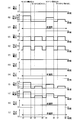
- FIG. 3 is a timing chart showing the concept of an operation example of the memory circuit according to the present embodiment.
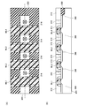
- FIG. 4 is a diagram for explaining a first structural example of a memory block which is a main part of the memory circuit according to the present embodiment and a method for manufacturing the memory block.
- FIG. 5 is a diagram for explaining a first structural example of a memory block, which is a main part of the memory circuit according to the present embodiment, and a manufacturing method thereof.
- FIG. 1 is a circuit diagram showing a circuit configuration example of the memory circuit according to the present embodiment.
- FIG. 2 is a circuit diagram illustrating another circuit configuration example of the memory circuit according to the present embodiment.
- FIG. 3 is a timing chart showing the concept of an operation example of the memory circuit according to the present embodiment.
- FIG. 4 is
- FIG. 6 is a diagram for explaining a first structural example of a memory block which is a main part of the memory circuit according to the present embodiment and a method for manufacturing the same.
- FIG. 7 is a diagram for explaining a first structural example of a memory block which is a main part of the memory circuit according to the present embodiment and a method for manufacturing the same.
- FIG. 8 is a diagram for explaining a first structural example of a memory block, which is a main part of the memory circuit according to the present embodiment, and a manufacturing method thereof.
- FIG. 9 is a diagram for explaining a first structure example of a memory block which is a main part of the memory circuit according to the present embodiment and a manufacturing method thereof.
- FIG. 10 is a diagram for explaining a first structural example of a memory block, which is a main part of the memory circuit according to the present embodiment, and a manufacturing method thereof.
- FIG. 11 is a diagram for explaining a second structural example of a memory block which is a main part of the memory circuit according to the present embodiment and a manufacturing method thereof.
- FIG. 12 is a diagram for explaining a second structural example of the memory block which is a main part of the memory circuit according to the present embodiment and a manufacturing method thereof.
- FIG. 13 is a diagram for explaining a second structure example of the memory block, which is a main part of the memory circuit according to the present embodiment, and a manufacturing method thereof.
- FIG. 11 is a diagram for explaining a second structural example of a memory block which is a main part of the memory circuit according to the present embodiment and a manufacturing method thereof.
- FIG. 12 is a diagram for explaining a second structural example of the memory block which is a main part of the memory circuit according to the present embodiment and a manufacturing
- FIG. 14 is a diagram for explaining a second structural example of a memory block which is a main part of the memory circuit according to the present embodiment and a manufacturing method thereof.
- FIG. 15 is a diagram for explaining a second structure example of the memory block, which is a main part of the memory circuit according to the present embodiment, and a manufacturing method thereof.
- FIG. 16A shows an example in which one memory cell block shares one bit line contact in the memory block of the first structure example.
- FIG. 16B shows two memory cell blocks in the second structure example.
- FIG. 6 is a cross-sectional view showing an example in which one bit line contact is shared by memory cell blocks.
- FIG. 17 is a configuration example of an integrated circuit device according to this embodiment.
- FIG. 18A is a configuration example of an electronic apparatus according to this embodiment.
- FIG. 18B is a configuration example of the electronic apparatus according to the present embodiment.
- FIG. 18C is a configuration example of the electronic apparatus according to the present embodiment.
- FIG. 1 is a circuit diagram showing a circuit configuration example of a memory circuit according to the present embodiment.
- the memory circuit 1 includes a memory cell including a transistor and a resistance change element having one end connected to one of a source and a drain of the transistor, and the first to Nth transistors as the transistors.
- a memory block 10 including N memory cells connected in series up to transistors is included.
- the number N of memory cells may be arbitrarily set as an integer of 2 or more.
- the memory block 10 includes four memory cells Cell-1 to Cell-4.
- a memory cell Cell ⁇ includes a first transistor T1 and a resistance change element RC1 having one end connected to one of the source and drain of the first transistor T1 (for example, the source; the same shall apply hereinafter).
- a memory cell Cell-2 including a second transistor T2 and a resistance change element RC2 having one end connected to one of the source and drain of the second transistor T2, and a third transistor T3.
- a memory cell Cell-3 including a resistance change element RC3 having one end connected to one of the source and the drain of the third transistor T3 is configured, and one of the source and the drain of the fourth transistor T4 and the fourth transistor T4
- a memory cell Cell-4 having a resistance change element RC4 having one end connected to one end is formed.
- the other of the source and the drain of the first transistor T1 (for example, the drain; the same applies hereinafter) is connected to the bit line BL1.
- four transistors from the first transistor T1 to the fourth transistor T4 are connected in series. That is, one of the source and the drain of the first transistor T1 is connected to the other of the source and the drain of the second transistor T2.
- One of the source and the drain of the second transistor T2 is connected to the other of the source and the drain of the third transistor T3.
- One of the source and the drain of the third transistor T3 is connected to the other of the source and the drain of the fourth transistor T4.
- the gates of the first transistor T1 to the fourth transistor T4 connected in series are connected to different word lines.
- the gate of the first transistor T1 is on the word line WL1
- the gate of the second transistor T2 is on the word line WL2
- the gate of the third transistor T3 is on the word line WL3
- the gate of the fourth transistor T4 is on Each is connected to the word line WL4.
- any one of the source and drain of the first transistor T1 to the fourth transistor T4 connected in series is connected to different program lines via at least different resistance change elements.
- one of the source and the drain of the first transistor T1 is connected to the program line PL1 via the resistance change element RC1
- one of the source and the drain of the second transistor T2 is the resistance change element.
- One of the source and drain of the third transistor T3 is connected to the program line PL3 via the resistance change element RC3
- one of the source and drain of the fourth transistor T4 is the resistor through the RC2 to the program line PL2.
- the change line RC4 is connected to the program line PL4, respectively.
- the memory circuit 1 includes variable resistance elements RC1 to RC4.
- the resistance change elements RC1 to RC4 include a plurality of carbon nanotubes existing between two electrodes, and the distance between the plurality of carbon nanotubes is changed, so that the resistance change elements RC1 to RC4 are relatively low resistance and relatively low resistance state. It takes one of the high resistance states that result in high resistance. Details of the resistance change elements RC1 to RC4 will be described later.
- the memory circuit 1 may include a control circuit 20.
- the control circuit 20 applies voltage and current between the two electrodes of the resistance change elements RC1 to RC4 by applying voltage and current to at least one of the bit line BL1, the word lines WL1 to WL4, and the program lines PL1 to PL4. Then, the state of the resistance change elements RC1 to RC4 is changed to either the low resistance state or the high resistance state.
- the control circuit 20 can apply different voltages and currents to the bit line BL1, the word lines WL1 to WL4, and the program lines PL1 to PL4 at different timings. That is, the bit line BL1, the word lines WL1 to WL4, and the program lines PL1 to PL4 are independent control lines.
- control circuit 20 includes a BL control circuit 202 for applying a voltage to the bit line BL1, a WL control circuit 204 for applying a voltage to the word lines WL1 to WL4, and a voltage to the program lines PL1 to PL4. And a PL control circuit 206 for applying a current.
- FIG. 2 is a circuit diagram illustrating another circuit configuration example of the memory circuit according to the present embodiment. Although the memory circuit 2 shown in FIG. 2 shows an example having two memory blocks 11 and 12, the memory circuit 2 may have three or more memory blocks.
- the memory circuit 2 may include a control circuit 21.
- the control circuit 21 applies voltage and current to at least one of the bit lines BL1 and BL2, the word lines WL1 to WL4, and the program lines PL1 to PL4, so that the resistance change elements RC11 to RC14 and RC21 to RC24 are connected between the two electrodes.
- a voltage and a current are applied to the resistance change elements RC11 to RC14 and RC21 to RC24 to change the state between the low resistance state and the high resistance state.
- the control circuit 21 can apply different voltages and currents to the bit lines BL1 and BL2, the word lines WL1 to WL4, and the program lines PL1 to PL4 at different timings.
- the bit lines BL1 and BL2, the word lines WL1 to WL4, and the program lines PL1 to PL4 are independent control lines.
- the control circuit 21 includes a BL control circuit 212 for applying a voltage to the bit lines BL1 and BL2, a WL control circuit 214 for applying a voltage to the word lines WL1 to WL4, and program lines PL1 to PL4.
- a PL control circuit 216 for applying a voltage and a current is included.
- the memory block 11 includes four memory cells Cell-11 to Cell-14.
- the memory cell Cell-11 including the first transistor T11 and the resistance change element RC11 having one end connected to either the source or the drain of the first transistor T11 is configured, and the second transistor T12 And a memory cell Cell-12 having a resistance change element RC12 having one end connected to one of the source and drain of the second transistor T12, and the third transistor T13 and the source and drain of the third transistor T13.
- a memory cell Cell-14 including the element RC14 is configured. That.
- the memory block 11 four transistors from the first transistor T11 to the fourth transistor T14 are sequentially connected in series. That is, one of the source and the drain of the first transistor T11 is connected to the other of the source and the drain of the second transistor T12. One of the source and the drain of the second transistor T12 is connected to the other of the source and the drain of the third transistor T13. One of the source and the drain of the third transistor T13 is connected to the other of the source and the drain of the fourth transistor T14.
- the memory block 12 includes four memory cells Cell-21 to Cell-24.
- a memory cell Cell-21 including a first transistor T21 and a resistance change element RC21 having one end connected to either the source or the drain of the first transistor T21 is configured, and the second transistor T22 And a memory cell Cell-22 having a resistance change element RC22 having one end connected to one of the source and drain of the second transistor T22, and the third transistor T23 and the source and drain of the third transistor T23.
- a memory cell Cell-24 including the element RC24 is configured. That.
- the memory block 12 four transistors from the first transistor T21 to the fourth transistor T24 are connected in series. That is, one of the source and the drain of the first transistor T21 is connected to the other of the source and the drain of the second transistor T22. One of the source and the drain of the second transistor T22 is connected to the other of the source and the drain of the third transistor T23. One of the source and the drain of the third transistor T23 is connected to the other of the source and the drain of the fourth transistor T24.
- the resistance change elements RC11 to RC14 and RC21 to RC24 include a plurality of carbon nanotubes existing between two electrodes, and have a low resistance state having a relatively low resistance and a high resistance state having a relatively high resistance. Take one of the states. Details of the resistance change elements RC11 to RC14 and RC21 to RC24 will be described later.
- At least one of the first transistors included in the plurality of memory blocks may be connected to different bit lines.
- one of the source and the drain of the first transistor T11 included in the memory block 11 is on the bit line BL1
- one of the source and the drain of the first transistor T12 included in the memory block 12 is included. The other is connected to the bit line BL2.
- a bit line, a word line, and a program line may be shared in a plurality of memory blocks.
- the memory block 11 and the memory block 12 share the word line and the program line.
- the word line WL1 is the gate of the first transistor T11 and the gate of the first transistor T21
- the word line WL2 is the gate of the second transistor T12 and the gate of the second transistor T22
- the word line WL3 is the gate of the third transistor T13 and the gate of the third transistor T13.
- the word line WL4 is connected to the gate of the third transistor T23 and the gate of the fourth transistor T14 and the gate of the fourth transistor T24, respectively.
- the program line PL1 is connected to the resistance change elements RC11 and RC21
- the program line PL2 is connected to the resistance change elements RC12 and RC22
- the program line PL3 is connected to the resistance change elements RC13 and RC23
- the program line PL4 is connected to the resistance change elements RC14 and RC24. Each is connected.
- one bit line may be connected to the first transistors of a plurality of memory cells.
- the area of the bit line contact can be shared by the two memory blocks, and the area of the memory chip can be reduced.
- the bit line contact at the center has an advantage that the resistance from the bit line to each transistor is reduced.
- one end of the first transistor T1 is connected to the bit line BL1, and the four transistors share one bit line, so that one transistor uses one bit line.
- the degree of circuit integration can be increased.
- the resistance change elements RC1 to RC4, RC11 to RC14, and RC21 to RC24 include a plurality of carbon nanotubes existing between two electrodes, and are relatively in a low resistance state where the resistance is relatively low.
- One of the high resistance states in which the resistance is high is obtained. That is, the resistance change elements RC1 to RC4, RC11 to RC14, and RC21 to RC24 in the present embodiment can function as switching elements.
- variable resistance elements RC1 to RC4, RC11 to RC14, and RC21 to RC24 in the present embodiment the voltage or current is not applied between the two electrodes from the control circuit 20 or the control circuit 21, or the power supply is cut off. In some cases, the high resistance state or the low resistance state is maintained. Further, the resistance change elements RC1 to RC4, RC11 to RC14, and RC21 to RC24 change to either a high resistance state or a low resistance state when a voltage and a current are applied between the two electrodes. That is, the resistance change elements RC1 to RC4, RC11 to RC14, and RC21 to RC24 in this embodiment can function as nonvolatile switching elements.
- the resistance change elements RC1 to RC4, RC11 to RC14, and RC21 to RC24 in the present embodiment are resistant to heat generated by the first voltage V1 and the first current Ip1 applied between the two electrodes from the control circuit 20 or the control circuit 21.
- the low resistance state may be changed to the high resistance state by changing the distance between the plurality of carbon nanotubes included in the change elements RC1 to RC4, RC11 to RC14, and RC21 to RC24.
- the resistance change elements RC1 to RC4, RC11 to RC14, and RC21 to RC24 have resistance by the Coulomb force based on the second voltage V2 and the second current Ip2 applied between the control circuit 20 or the control circuit 21 and the two electrodes.
- the high resistance state may be changed to the low resistance state by changing the distance between the plurality of carbon nanotubes included in the change elements RC1 to RC4, RC11 to RC14, and RC21 to RC24.
- the resistance change elements RC1 to RC4, RC11 to RC14, and RC21 to RC24 are included in the resistance change element by the first voltage V1 and the first current Ip1 applied between the two electrodes from the control circuit 20 or the control circuit 21. Due to heat generated by the current flowing through the carbon nanotubes, the distance between the plurality of carbon nanotubes changes from a positional relationship in which the two electrodes are electrically connected to a positional relationship in which the electrodes are not electrically connected. Changes to a high resistance state. Further, the position where the two electrodes are not electrically connected by the Coulomb force generated by the electric field generated by the second voltage V2 and the second current Ip2 applied between the two electrodes from the control circuit 20 or the control circuit 21. By changing from the relationship to a positional relationship in which the electrodes are electrically connected, the high resistance state is changed to the low resistance state.
- the first current Ip1 may be larger than the second current Ip2.
- the first voltage V1 may be larger than the second voltage V2.
- the heat generation is Joule heat generated by the current flowing through the carbon nanotubes, but it may be heat generation by Joule heat generated by the resistance of the heat generation part (electrode, connection portion thereof, etc.) in the region close to the carbon nanotubes.
- Carbon nanotubes have a good thermal conductivity and easily transmit locally generated heat.
- the setting of the first current value Ip1 is important. It is desirable to set the current value according to the size of the circuit, the internal resistance of the incorporated transistor, the resistance of the wiring portion, and the like.
- the first current Ip1 is set so that Ip1> Ip2 is satisfied when the current flowing through the variable resistance element is the second current Ip2.
- Such resistance change elements RC1 to RC4, RC11 to RC14, and RC21 to RC24 in this embodiment can operate as a high-speed switch element as compared with a method of storing charges such as a DRAM or a flash memory. Therefore, the memory circuit 1 and the memory circuit 2 that can read and write at high speed can be realized.
- the resistance change elements RC1 to RC4, RC11 to RC14, and RC21 to RC24 in the present embodiment are not affected by the amount of charge compared to a method of storing charges such as DRAM and flash memory, so that the memory is miniaturized. In this case, the amount of stored charge does not decrease. For this reason, even if the memory circuit is miniaturized, the retention period of the stored state is longer than that of the charge storage type nonvolatile memory.
- the structure itself for storing charges becomes smaller as the structure becomes finer. Therefore, less charge is used for storing data representing “1” and data representing “0” (ON and OFF) in the nonvolatile memory. As a result, the difference between the data representing “1” and the data representing “0” (ON and OFF) due to the amount of charge becomes small, and the difference between the data representing “1” and the data representing “0” is unclear. Therefore, there is a limit to miniaturization while maintaining reliability.
- the ON / OFF mechanism the switching principle between the low resistance state and the high resistance state
- the resistance change element in the present embodiment is not related to the amount of charge. Therefore, it is possible to eliminate the limitation of miniaturization in the structure of the conventional flash memory.
- the memory circuit 1 and the memory circuit 2 that can hold data for a long period of time can be realized even if the memory circuit is miniaturized and highly integrated.
- the resistance change elements RC1 to RC4, RC11 to RC14, and RC21 to RC24 in the present embodiment are more resistant to state changes than a configuration in which electrons pass through the insulating oxide film of a transistor, such as a flash memory. high. Therefore, the memory circuit 1 and the memory circuit 2 having a long rewrite life can be realized.
- the resistance change elements RC1 to RC4, RC11 to RC14, and RC21 to RC24 in the present embodiment may include conductive carbon nanotubes. Furthermore, it is preferable that the resistance change elements RC1 to RC4, RC11 to RC14, and RC21 to RC24 contain more metallic (conductive) carbon nanotubes than semiconducting carbon nanotubes. By including many metallic carbon nanotubes, the difference in resistance value between the low resistance state and the high resistance state increases. Therefore, a difference in reading between data representing “1” and data representing “0” becomes clear, and good memory characteristics with high reliability can be obtained.
- the resistance change elements RC1 to RC4, RC11 to RC14, and RC21 to RC24 in the present embodiment preferably include more single wall carbon nanotubes than multiwall carbon nanotubes.
- Metallic single-walled carbon nanotubes are characterized by being easily affected by Coulomb force and being easily bent, and being easily deformed by vibration (lattice scattering) due to Joule heat. Therefore, the difference in resistance value between the low resistance state and the high resistance state becomes large, and good memory characteristics can be obtained.
- FIG. 3 is a timing chart showing a concept of an operation example of the memory circuit 2 according to the present embodiment. Since FIG. 3 illustrates the concept, it does not take into account each voltage, a margin of current application timing, a time variation of an actual waveform, and the like.
- 3A is a voltage applied to the bit line BL1 from the BL control circuit 212
- FIG. 3B is a current flowing through the bit line BL1
- FIG. 3C is a BL control.
- 3D is applied to the word line WL1 from the WL control circuit 214
- FIG. 3E is applied to the word line WL2 from the WL control circuit 214.
- 3F is a voltage applied to the word line WL3 from the WL control circuit 214, FIG.
- FIG. 3G is a voltage applied to the word line WL4 from the WL control circuit 214
- FIG. 3H is a PL control.
- the voltage applied to the program line PL1 from the circuit 216 FIG. 3I is applied to the program line PL2 from the PL control circuit 216
- FIG. 3J is applied to the program line PL2 from the PL control circuit 216.
- Current, 3 (K) is a voltage applied to the program line PL3 from PL control circuit 216
- FIG. 3 (L) represents a voltage applied to the program line PL4 from PL control circuit 216.
- the timing chart shown in FIG. 3 shows an example in which a voltage at the time of reading is applied from the PL control circuit 216.
- the program lines PL1 to PL4 are set to the ground level (0 V), and the selected bit lines BL1 to BL2 are selected. Similarly, data representing “0” and “1” can be read at the current levels of the bit lines BL1 to BL2 even when a read voltage is applied to the side.
- FIG. 3 shows an operation of writing data to the resistance change element RC12 of the memory cell Cell-12 and an operation of reading data written to the resistance change element RC12.
- the description will be given with reference. Further, it is assumed that data representing “1” is written in the resistance change element RC12 when the resistance change element RC12 is in the low resistance state, and “0” is represented when the resistance change element RC12 is in the high resistance state. It is assumed that data is written in the resistance change element RC12.
- a period from time t1 to time t2 is a period in which data representing “0” is written to the resistance change element RC12.
- a period from time t3 to time t4 is a period in which data representing “0” written in the period from time t1 to time t2 is read from the resistance change element RC12.
- a period from time t5 to time t6 is a period in which data representing “1” is written to the resistance change element RC12.
- the period from time t7 to time t8 is a period in which data representing “1” written in the period from time t5 to time t6 is read from the resistance change element RC12.
- the first voltage V1 and the first current Ip1 are applied to the program line PL2 (FIGS. 3I and 3J), and the word lines WL1 and WL2 have transistors T11 and T12. Is applied (FIGS. 3D and 3E).
- the transistor T11 only serves as a switch.
- 0V ground potential
- 0V is applied to the bit line BL1 and the word lines WL3 and WL4 (FIGS. 3A, 3F, and 3G).
- T13, T14, T23, and T24 are turned off.
- the bit line BL2, the program lines PL1, PL3, and PL4 are in a non-selected state (high impedance) (FIGS. 3C, 3H, 3K, and 3L).
- the state of the resistance change element RC12 once becomes a low resistance state, heat is generated by the current Ip1 flowing between the program line PL2 and the bit line BL1 via the resistance change element RC12, and a change in the distance between the plurality of carbon nanotubes occurs.
- the carbon nanotubes that are electrically connected between the two electrodes change to a state where they are not electrically connected.
- the current through the RC 12 does not flow and heat generation stops. That is, the state of the resistance change element RC12 changes from the low resistance state to the high resistance state. As a result, data representing “0” is written to the resistance change element RC12.
- a read voltage Vr and a very small read current Ipr are applied to the program line PL2 (FIGS. 3I and 3J).
- the read voltage Vr is a voltage that does not change the state of the resistance change element RC12, and is a voltage lower than the first voltage V1 and the second voltage V2. That is, the magnitude relationship among the first voltage V1, the second voltage V2, and the read voltage Vr is expressed by the inequality V1> V2> Vr.
- the magnitude relationship among the first current Ip1, the second current Ip2, and the read current Ipr is expressed by the inequality Ip1> Ip2> Ipr.
- V1, V2, and Vr and the relationship between Ip1, Ip2, and Ipr are preferably optimized as appropriate depending on the values of the transistor internal resistance and the wiring resistance of the memory blocks 11 and 12.
- a gate voltage Vh at which the transistor T11 and the transistor T12 are turned on (ON state) is applied to the word line WL1 and the word line WL2 (FIGS. 3D and 3E).
- 0V (ground potential) is applied to the bit line BL1 and the word lines WL3 and WL4 (FIGS. 3A, 3F, and 3G).
- the bit line BL2, the program lines PL1, PL3, and PL4 are in a non-selected state (high impedance) (FIGS. 3C, 3H, 3K, and 3L).
- the voltage on the resistance change element side corresponding to the drain side of the transistors T12 and T11 is not high enough to turn on the series transistor because the resistance change element is in a high resistance state, and is connected in series with the transistors T11 and T12.
- the transistor is not completely turned on, and since the variable resistor is in a high resistance state, the flowing current becomes very small. Accordingly, no large current flows through the bit line BL1 (FIG. 3B).
- the reference current value Iref is set to satisfy Iref> Ibs, and the current is smaller than the reference current Iref by comparing the reference current value Iref and the current Ibs on the BL control circuit 212 side. It can be determined that the resistance state is high.
- the state of the resistance change element RC12 does not change by the read voltage Vr and the read current Ipr, the data written in the resistance change element RC12 is not changed without changing all the states of the resistance change elements RC11 to RC14 and RC21 to RC24. Can be read.
- the second voltage V2 and the second current Ip2 are applied to the program line PL2 (FIGS. 3I and 3J), and the word line WL1 and the word line WL2 have the transistor T11 and A gate voltage Vh that turns on the transistor T12 is applied (FIGS. 3D and 3E).
- 0V ground potential
- the bit line BL2, the program lines PL1, PL3, and PL4 are in a non-selected state (high impedance) (FIGS. 3C, 3H, 3K, and 3L).
- the second current Ip2 is a smaller value than Ip1.
- the current flowing through the resistance change element RC12 by the current Ip2 applied from the PL control circuit 216 is a second current Ip2 smaller than the first current Ip1.
- the state of the resistance change element RC12 does not change from the low resistance state to the high resistance state due to a change in the distance between the plurality of carbon nanotubes based on heat generation by the current Ip2 flowing through the resistance change element RC12. Therefore, the state of the resistance change element RC12 becomes a low resistance state. As a result, data representing “1” is written in the resistance change element RC12.
- a read voltage Vr and a very small read current Ipr are applied to the program line PL2 (FIGS. 3I and 3J).
- a gate voltage Vh at which the transistor T11 and the transistor T12 are turned on (ON state) is applied to the word line WL1 and the word line WL2 (FIGS. 3D and 3E).
- 0V (ground potential) is applied to the bit line BL1 and the word lines WL3 and WL4 (FIGS. 3A, 3F, and 3G).
- the bit line BL2, the program lines PL1, PL3, and PL4 are in a non-selected state (high impedance) (FIGS. 3C, 3H, 3K, and 3L).
- the voltage on the resistance change element side corresponding to the drain side of the transistors T12 and T11 connected in series is a series transistor on the drain side of the transistors T11 and T12 connected in series because the resistance change element is in a low resistance state. Since the voltage value is sufficient to turn ON, the series transistors T11 and T12 are turned on. Therefore, a large ON current Ibr flows through the bit line BL1 (FIG. 3B).
- the magnitude relationship between the current Ibr and the current Ibs is expressed by the inequality Ibr> Ibs.
- the reference current value Iref is set to satisfy Ibr> Iref> Ibs, and the resistance change element RC12 is in the low resistance state by comparing the reference current value Iref and the current Ibr on the BL control circuit 212 side. Can be determined. Thereby, data representing “1” written in the resistance change element RC12 during the period from time t5 to time t6 can be read from the resistance change element RC12. Further, since the state of the resistance change element RC12 does not change with the read voltage Vr, the data written in the resistance change element RC12 can be read without changing all the states of the resistance change elements RC11 to RC14 and RC21 to RC24. .
- the control circuit 21 applies a predetermined voltage to the bit lines BL1, BL2, the word lines WL1 to WL4, and the program lines PL1 to PL4 so that a voltage and a current are applied between the two electrodes of the variable resistance element to be operated.
- a current by applying a current, a memory circuit 2 that can be randomly accessed for each bit can be realized.
- data representing “0” is selectively written into the memory cell Cell-12, data representing “0” is read, data representing “1” is written, and “1” is written.
- the basic operation of reading out the data representing " is described.
- an operation of reading data in a memory cell and rewriting it to data representing “0” or data representing “1” can be performed only when the data is to be rewritten. By doing so, the rewriting efficiency can be improved.
- the memory circuit 1 and the memory circuit 2 according to the present embodiment can read bit by bit without destroying data stored in other memory cells. Therefore, the number of steps for reading (transistor switching operation, etc.) is smaller than that of a conventional NAND flash memory. Therefore, although it is a NAND type memory circuit that can be highly integrated, it can be read at a higher speed than the conventional NAND type flash memory.
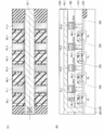
- FIG. 4A is a plan view of a memory block
- FIG. 4B is a cross-sectional view taken along a dashed line in FIG. 4A.
- a method for manufacturing a memory block of the memory circuit according to the present embodiment on a silicon substrate will be described.
- an element isolation film 302 is formed on the main surface side of a P-type silicon substrate 300.
- the element isolation film 302 may be formed by a known STI (shallow trench isolation) method or a LOCOS (local oxidation of silicon) method.
- the element isolation film 302 is formed by the STI method.
- a double well structure in which an N type well or a P type well is formed in an N type well in the P type silicon substrate 300 may be used.
- a gate insulating film 304 is formed in the element formation region on the surface of the P-type silicon substrate 300.
- the gate insulating film 304 may be formed by forming a silicon oxide film by thermally oxidizing the surface of the P-type silicon substrate 300.
- a composite film of a silicon oxide film and a silicon nitride film Si 3 N 4 film may be used.
- word lines WL 1 to WL 4 are formed on the gate insulating film 304.
- the word lines WL1 to WL4 may be formed by the following procedure. First, a polysilicon layer is deposited, and a silicon nitride film (Si 3 N 4 film) to be the cap layer 310 is deposited thereon. Thereafter, a desired resist pattern is formed by a photolithography process using a mask, and then patterned using a dry etching method such as a reactive ion etching (RIE) method using the resist pattern as a mask, A desired WL pattern is formed by removing the resist film.
- RIE reactive ion etching
- an n-type diffusion layer 306 is formed.
- an n ⁇ type diffusion region is formed as the n type diffusion layer 306 by implanting phosphorus (P) ions, arsenic (As) ions, or the like by ion implantation using the word lines WL1 to WL4 as a mask.
- the n-type diffusion layer 306 is not formed in the channel region directly under the gate.
- sidewall films 308 are formed on both sides of the word lines WL1 to WL4.
- the sidewall film 308 is formed by depositing a silicon oxide film over the entire surface of the substrate using a CVD method and then etching the entire surface using an anisotropic dry etching method such as a reactive dry etching (RIE) method.
- RIE reactive dry etching
- n + -type diffusion region is formed.
- a region immediately below the gate becomes a low-concentration n ⁇ -type diffusion region, and other regions become high-concentration n + -type diffusion regions.
- LDD lightly doped drain
- the cap film 310 formed on the word lines WL1 to WL4 serves to increase the step difference of the gate electrode when forming the sidewall film 308 and to increase the thickness of the mask when ion implantation is performed using the gate electrode as a mask. This has the effect of preventing ions from penetrating into the channel region.
- an interlayer insulating film 312 is formed on the main surface side of the P-type silicon substrate 300.
- the interlayer insulating film 312 may be formed of a silicon oxide film formed by a CVD (chemical vapor deposition) method. Thereafter, the interlayer insulating film 312 may be planarized using a CMP (chemical mechanical polishing) method or the like.
- a contact hole (through hole) that penetrates the interlayer insulating film 312 and reaches the surface of the n + -type diffusion region of the n-type diffusion layer 306 is formed.
- the contact hole is formed by removing the interlayer insulating film 312 in a desired region by etching using photolithography, RIE, or the like.
- a titanium film (Ti) and a titanium nitride film (TiN) are deposited on the entire surface of the substrate by PVD (physical vapor deposition) so as to cover the side wall and bottom surface of the contact hole.
- a tungsten film (W) is deposited using a CVD method, and then a tungsten film, a titanium nitride film, and a titanium film are selectively embedded in the contact hole by a CMP method to form a via 314 serving as a tungsten plug.
- a lower electrode 316 is formed on the entire surface.
- the lower electrode 316 may be formed using a titanium nitride film formed by a sputtering method.
- the via 314 buried in the contact hole and the lower electrode 316 are formed so as to be electrically connected.
- a carbon nanotube layer 318 is formed on the entire surface of the lower electrode 316.
- the carbon nanotube layer 318 may be formed by applying a dispersion containing carbon nanotubes by spin coating or the like.
- the upper electrode 320 is formed on the entire surface of the carbon nanotube layer 318.
- the upper electrode 320 may be formed of a titanium nitride film formed by a sputtering method.
- the upper electrode 320, the carbon nanotube layer 318, and the lower electrode 316 are formed in the bit line direction (the bit formed in a later step as shown in FIG. 7A) by using a normal photolithography method and a dry etching method. It is processed into an elongated shape in the longitudinal direction of the line BL1. Thereafter, the resist film (not shown) used for processing is removed.
- a tungsten film to be the program lines PL1 to PL4 is deposited on the entire surface by a CVD method or the like, the tungsten film, The upper electrode 320, the carbon nanotube layer 318, and the lower electrode 316 are continuously processed.
- program lines PL1 to PL4 electrically connected to the upper electrode 320 and connected in the longitudinal direction of the word lines WL1 to WL4 are formed.
- the lower electrode 316, the carbon nanotube layer 318, and the upper electrode 320 are formed independently for each memory cell.
- Lower electrode 316 is electrically joined to either the source or the drain of the transistor, and upper electrode 320 is electrically connected to program lines PL1 to PL4.
- an interlayer insulating film 322 is formed so as to cover the program lines PL 1 to PL 4 and the interlayer insulating film 312.
- the interlayer insulating film 322 may be formed using a silicon oxide film formed by a CVD method.
- the interlayer insulating film 322 is planarized by a CMP method. Thereafter, a contact hole (through-hole) 324 that penetrates the interlayer insulating film 312 and the interlayer insulating film 322 and reaches the surface of the n + -type diffusion region of the n-type diffusion layer 306 is formed.
- the contact hole 324 may be formed by removing the interlayer insulating film 312 and the interlayer insulating film 322 in a desired region by a dry etching process using photolithography and an RIE method.
- the bit line BL 1 electrically connected to the n + -type diffusion region of the n-type diffusion layer 306 through the contact hole 324 is connected to the insulating interlayer film 322.
- the bit line BL1 may be formed by forming a tungsten film formed by a CVD method and then removing unnecessary portions by photolithography, etching, or the like.
- an interlayer insulating film 324 is formed so as to cover the bit line BL1 and the interlayer insulating film 322.
- the interlayer insulating film 324 may be formed using a silicon oxide film formed by a CVD method.
- an ordinary metal wiring process is performed to form an interlayer insulating film, pad opening, necessary sintering heat treatment, and the like, and an LSI (large scale integration) is completed.
- the cross-sectional view shown in FIG. 10B of the memory block thus formed is compared with the circuit diagram shown in FIG.
- the transistor T1 using the word line WL1 as a gate and the n-type diffusion layer 306 as a source or drain, and the word line WL2 as a gate and the n-type diffusion layer 306 as a source or drain It can be seen that the transistor T2, the transistor T3 having the word line WL3 as a gate and the n-type diffusion layer 306 as a source or drain, and the transistor T4 having the word line WL4 as a gate and the n-type diffusion layer 306 as a source or drain are formed. .
- variable resistance elements RC1 to RC4 each including the lower electrode 316, the carbon nanotube layer 318, and the upper electrode 320 are formed. That is, it can be seen that the configuration shown in FIG. 10B corresponds to the memory block 10 in the circuit diagram shown in FIG.
- the degree of integration of the memory circuit can be increased.
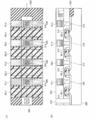
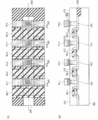
- FIGS. 11 to 15 are views for explaining a second structure example of the memory block which is a main part of the memory circuit according to the present embodiment and a manufacturing method thereof.
- A) in each figure is a plan view of the memory block
- B) in each figure is a cross-sectional view taken along the alternate long and short dash line in (A) of the figure.
- symbol is attached
- a recess is formed by recess etching a part of the tungsten film in the contact hole 314, and a lower electrode 316 is formed in the recess.
- a titanium nitride film formed by sputtering is deposited on the entire surface, and then planarized by CMP to selectively form the lower electrode 316 in the recess.
- a carbon nanotube layer 318 is formed on the entire surface so as to be electrically connected to the lower electrode 316 embedded in the recess.
- the carbon nanotube layer 318 may be formed by applying a dispersion containing carbon nanotubes by spin coating or the like.
- the upper electrode 320 is formed on the carbon nanotube layer 318.
- the upper electrode 320 may be formed of a titanium nitride film formed by a sputtering method.
- the carbon nanotube layer 318 and the upper electrode 320 are processed into a desired shape elongated in the bit line direction (longitudinal direction of the bit line BL1 formed in a later step) by using photolithography, etching, or the like.
- a tungsten film to be the program lines PL1 to PL4 is deposited on the entire surface by a CVD method or the like, and then the tungsten film, The upper electrode 320 and the carbon nanotube layer 318 are continuously processed.
- program lines PL1 to PL4 electrically connected to the upper electrode 320 and connected in the longitudinal direction of the word lines WL1 to WL4 are formed.
- the lower electrode 316, the carbon nanotube layer 318, and the upper electrode 320 are formed independently for each memory cell.
- Lower electrode 316 is electrically joined to either the source or the drain of the transistor, and upper electrode 320 is electrically connected to program lines PL1 to PL4.
- an interlayer insulating film 322 is formed so as to cover the program lines PL 1 to PL 4 and the interlayer insulating film 312.
- the interlayer insulating film 322 may be formed using a silicon oxide film formed by a CVD method.
- the interlayer insulating film 322 is planarized by a CMP method. Thereafter, a contact hole (through-hole) 324 that penetrates the interlayer insulating film 312 and the interlayer insulating film 322 and reaches the surface of the n + -type diffusion region of the n-type diffusion layer 306 is formed.
- the contact hole 324 may be formed by removing the interlayer insulating film 312 and the interlayer insulating film 322 in a desired region by photolithography, etching, or the like.
- the bit line BL 1 electrically connected to the n + -type diffusion region of the n-type diffusion layer 306 through the contact hole 324 is connected to the insulating interlayer film 322.
- the bit line BL1 may be formed by using a tungsten film formed by a CVD method and removing unnecessary portions by photolithography, etching, or the like.
- an interlayer insulating film 324 is formed so as to cover the bit line BL1 and the interlayer insulating film 322.
- the interlayer insulating film 324 may be formed using a silicon oxide film formed by a CVD method.
- an ordinary metal wiring process is performed to form an interlayer insulating film, pad opening, necessary sintering heat treatment, and the like, thereby completing the LSI.
- the cross-sectional view shown in FIG. 15B of the memory block thus formed is compared with the circuit diagram shown in FIG. According to the cross-sectional view shown in FIG. 15B, the transistor T1 having the word line WL1 as a gate and the n-type diffusion layer 306 as a source or drain, and the word line WL2 as a gate and the n-type diffusion layer 306 as a source or drain. It can be seen that the transistor T2, the transistor T3 having the word line WL3 as a gate and the n-type diffusion layer 306 as a source or drain, and the transistor T4 having the word line WL4 as a gate and the n-type diffusion layer 306 as a source or drain are formed. .
- variable resistance elements RC1 to RC4 each including the lower electrode 316, the carbon nanotube layer 318, and the upper electrode 320 are formed. That is, it can be seen that the configuration shown in FIG. 15B corresponds to the memory block 10 in the circuit diagram shown in FIG.
- a configuration in which one bit line is shared by a plurality of memory cells can increase the degree of integration of the memory circuit. Furthermore, the lower electrode 316 can be miniaturized by embedding the lower electrode 316 in the contact hole.
- FIG. 16A shows an example in which one memory cell block shares one bit line contact in the memory block of the first structure example.
- FIG. 16B shows two memory cell blocks in the second structure example.
- FIG. 6 is a cross-sectional view showing an example in which one bit line contact is shared by memory cell blocks.
- 16A and 16B are examples in which the memory block 11 and the memory block 12 are connected to the same bit line BL1.
- the memory block 11 and the memory block 12 are arranged around the bit line contact BC, and the two memory blocks of the memory block 11 and the memory block 12 share one bit line contact BC.
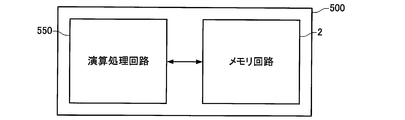
- FIG. 17 is a configuration example of an integrated circuit device according to this embodiment.
- An integrated circuit device 500 according to this embodiment includes a memory circuit 2 and an arithmetic processing circuit 550.
- the memory circuit 2 and the arithmetic processing circuit 550 may be formed on the same semiconductor substrate. Note that the memory circuit 1 may be included instead of the memory circuit 2.
- the arithmetic processing circuit 500 may perform various arithmetic processes using data stored in the memory circuit 2. Further, the arithmetic processing circuit 500 may store the results of performing various arithmetic processes in the memory circuit 2.
- an integrated circuit device including a memory circuit that is nonvolatile and can be accessed randomly for each bit or rewritten for each block and can increase the degree of circuit integration. realizable.
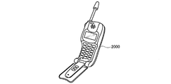
- FIGS. 18A to 18C are configuration examples of electronic devices according to the present embodiment.
- 18A shows a notebook computer 1000
- FIG. 18B shows a mobile phone 2000
- FIG. 18C shows an IC recorder 3000.
- the notebook personal computer 1000, the mobile phone 2000, and the IC recorder 3000 according to the present embodiment are configured to include the memory circuit 2 as a part of the storage device that each has. Further, the integrated circuit device 500 including the memory circuit 2 may be included.
- an electronic device including a memory circuit that is nonvolatile and can be randomly accessed for each bit or rewritten for each block and can increase the degree of circuit integration is realized. it can. Further, since a nonvolatile memory circuit is used, low power consumption can be realized.
- the present invention is not limited to the present embodiment, and various modifications can be made within the scope of the gist of the present invention.
- the present invention includes substantially the same configuration (for example, a configuration having the same function, method, and result, or a configuration having the same purpose and effect) as the configuration described in the embodiment.
- the invention includes a configuration in which a non-essential part of the configuration described in the embodiment is replaced.
- the present invention includes a configuration that achieves the same effect as the configuration described in the embodiment or a configuration that can achieve the same object.
- the invention includes a configuration in which a known technique is added to the configuration described in the embodiment.
Landscapes
- Engineering & Computer Science (AREA)
- Chemical & Material Sciences (AREA)
- Nanotechnology (AREA)
- Physics & Mathematics (AREA)
- Mathematical Physics (AREA)
- Theoretical Computer Science (AREA)
- Crystallography & Structural Chemistry (AREA)
- Manufacturing & Machinery (AREA)
- Semiconductor Memories (AREA)
Abstract
トランジスタと抵抗変化素子を備えるメモリセルを構成し、順に直列接続されたN個のメモリセルを含むメモリブロック10を含み、第1トランジスタT1の一端は、ビット線BL1に接続され、抵抗変化素子RC1~RC4は、2つの電極間に存在する複数のカーボンナノチューブを含み、相対的に低抵抗となる低抵抗状態と相対的に高抵抗となる高抵抗状態のいずれかの状態をとり、2つの電極間に電圧及び電流が印加されていない場合には、低抵抗状態又は高抵抗状態を保持する。
Description
本発明は、メモリ回路、集積回路装置及び電子機器に関する。
半導体記憶装置の代表格の1つであるDRAM(Dynamic Random Access Memory)は様々な電子機器において使用されている。これは、メモリセルの構成が1素子型(1トランジスタ及び1キャパシタ)であり、メモリセル自体の構造が単純で集積度を高めやすいからである。現在では1Gb(ギガビット)クラスの集積度のDRAMが製造されている。また、例えば、特開平4-3463号公報には、DRAMをさらに集積度を高めるための提案が開示されている。DRAMは、ある一定期間を過ぎると、メモリセル内のデータが破壊される性質がある。したがって、これを防ぐために、定期的にデータを読み出して再書き込みを行う、リフレッシュ動作が必要である。しかし、DRAMは電源を切るとデータが消えてしまう揮発性のメモリである。
また、近年では、電源を切ってもデータが消えない不揮発性メモリ(例えば、フラッシュメモリなど)が開発されている。フラッシュメモリはトンネル電流などを利用して浮遊ゲートと呼ばれる領域に電子を蓄積し、浮遊ゲートに電子があるかないかによりトランジスタのしきい値電圧が変化し、それにより「1」を表すデータと「0」を表すデータとを記憶する方式である。NAND構造のフラッシュメモリ(NAND型フラッシュとも呼ぶ)はビット線とソース線の間に浮遊ゲートと制御ゲートを積層した構造のものをビット線方向に16個あるいは32個並べたものである。現在では、8Gbや16Gbクラスのフラッシュメモリが製造されている。さらに最近においては、ReRAM(Resistivity Change Random Access Memory)としてMRAM(Magnetoresistive Random Access Memory)やPCM(Phase Change Memory)などの各種抵抗変化素子を用いたものが提案されている。その一つとして、国際公開第WO2008/021912号には、カーボンナノチューブを抵抗変化素子として用いた不揮発性メモリが開示されている。
しかしながら、NAND構造をとったDRAMである特開平4-3463号公報では集積度は向上できるがDRAMであり不揮発性ではない。また、国際公開第WO2008/021912号に記載の回路では、DRAMと同じようなメモリ回路構成をとるため集積度を高めることができないという問題点があった。
本発明は、以上のような問題点に鑑みてなされたものである。本発明のいくつかの態様によれば、不揮発性でありながら、ビットごとにランダムにアクセスすることも、ブロックごとのデータ消去を行いそのブロックのビットごとに書き込むことも可能であり、回路の集積度を高めたメモリ回路、集積回路装置及び電子機器を提供することができる。
(1)本発明に係るメモリ回路の態様の一つは、
トランジスタと、該トランジスタのソース及びドレインのいずれか一方に一端が接続された抵抗変化素子を備えるメモリセルを構成し、前記トランジスタとしての第1トランジスタ~第Nトランジスタまでが順に直列接続されたN個の前記メモリセルを含むメモリブロックを含み、
前記第1トランジスタのソース及びドレインのいずれか他方は、ビット線に接続され、
直列接続された前記トランジスタの各ゲートは、それぞれ異なるワード線に接続され、
直列接続された前記トランジスタのソース及びドレインのいずれか一方は、それぞれ異なる前記抵抗変化素子を介して、それぞれ異なるプログラム線に接続され、
前記抵抗変化素子は、
2つの電極間に存在する複数のカーボンナノチューブを含み、相対的に低抵抗となる低抵抗状態と相対的に高抵抗となる高抵抗状態のいずれかの状態をとり、
前記2つの電極間に電圧及び電流が印加されていない場合には、前記高抵抗状態又は前記低抵抗状態を保持し、
前記2つの電極間に電圧及び電流が印加されることにより、前記高抵抗状態と前記低抵抗状態のいずれかの状態に変化する。
トランジスタと、該トランジスタのソース及びドレインのいずれか一方に一端が接続された抵抗変化素子を備えるメモリセルを構成し、前記トランジスタとしての第1トランジスタ~第Nトランジスタまでが順に直列接続されたN個の前記メモリセルを含むメモリブロックを含み、
前記第1トランジスタのソース及びドレインのいずれか他方は、ビット線に接続され、
直列接続された前記トランジスタの各ゲートは、それぞれ異なるワード線に接続され、
直列接続された前記トランジスタのソース及びドレインのいずれか一方は、それぞれ異なる前記抵抗変化素子を介して、それぞれ異なるプログラム線に接続され、
前記抵抗変化素子は、
2つの電極間に存在する複数のカーボンナノチューブを含み、相対的に低抵抗となる低抵抗状態と相対的に高抵抗となる高抵抗状態のいずれかの状態をとり、
前記2つの電極間に電圧及び電流が印加されていない場合には、前記高抵抗状態又は前記低抵抗状態を保持し、
前記2つの電極間に電圧及び電流が印加されることにより、前記高抵抗状態と前記低抵抗状態のいずれかの状態に変化する。
本態様によれば、2つの電極間に存在する複数のカーボンナノチューブを含み、相対的に低抵抗となる低抵抗状態と相対的に高抵抗となる高抵抗状態のいずれかの状態をとる抵抗変化素子を用い、直列接続されたトランジスタのソース及びドレインのいずれか一方は、少なくともそれぞれ異なる抵抗変化素子を介して、それぞれ異なるプログラム線に接続されているため、ビットごとにランダムにアクセスできるメモリ回路や、抵抗変化素子をブロックごとに高抵抗状態(又は低抵抗状態)に変化させてからビットごとにデータを書き込んでいく不揮発性のメモリ回路を提供できる。
また、本態様によれば、順に直列接続された第1のトランジスタ~第NのトランジスタまでのN個のトランジスタのうち、第1のトランジスタの一端がビット線に接続され、N個のトランジスタで1本のビット線を共用するため、回路の集積度を高めることができる。
(2)このメモリ回路では、
前記抵抗変化素子は、前記2つの電極間に印加される第1電圧及び第1電流による発熱により前記複数のカーボンナノチューブ間の距離が変化することによって前記低抵抗状態から前記高抵抗状態に変化し、前記2つの電極間に印加される第2電圧及び第2電流に基づくクーロン力により前記複数のカーボンナノチューブ間の距離が変化することによって前記高抵抗状態から前記低抵抗状態に変化してもよい。
前記抵抗変化素子は、前記2つの電極間に印加される第1電圧及び第1電流による発熱により前記複数のカーボンナノチューブ間の距離が変化することによって前記低抵抗状態から前記高抵抗状態に変化し、前記2つの電極間に印加される第2電圧及び第2電流に基づくクーロン力により前記複数のカーボンナノチューブ間の距離が変化することによって前記高抵抗状態から前記低抵抗状態に変化してもよい。
(3)このメモリ回路では、
前記第1電流は前記第2電流よりも大きくてもよい。
前記第1電流は前記第2電流よりも大きくてもよい。
また、前記第1電圧は前記第2電圧よりも大きくてもよい。
(4)このメモリ回路では、
前記抵抗変化素子は、導電性のカーボンナノチューブを含んでもよい。
前記抵抗変化素子は、導電性のカーボンナノチューブを含んでもよい。
抵抗変化素子が導電性(金属性)のカーボンナノチューブを多く含むことにより、低抵抗状態と高抵抗状態の抵抗値の差が大きくなる。したがって、「1」を表すデータと「0」を表すデータとの読み出しの差が明確になり良好なメモリ特性が得られる。
(5)このメモリ回路では、
前記抵抗変化素子は、マルチウォールカーボンナノチューブよりもシングルウォールカーボンナノチューブを多く含んでもよい。
前記抵抗変化素子は、マルチウォールカーボンナノチューブよりもシングルウォールカーボンナノチューブを多く含んでもよい。
シングルウォールカーボンナノチューブは、非常に細いため電界などの力により曲がったり、熱的な振動によって屈曲が変化したりしやすい性質がある。すなわち、複数のカーボンナノチューブ間の距離の変化を起こしやすい。このため、抵抗変化素子の電極間にあるカーボンナノチューブ間が電気的に接続されていない高抵抗な状態からクーロン力で引き付けられることにより電気的に接続された低抵抗状態への変化や、熱による振動を受けて低抵抗状態から電気的に接続されていない高抵抗状態への変化を起こしやすい。したがって、「1」を表すデータと「0」を表すデータとの読み出しの差が明確になり良好なメモリ特性が得られる。
(6)このメモリ回路では、
前記ビット線、前記ワード線及び前記プログラム線の少なくとも1つに電圧及び電流を印加することにより前記抵抗変化素子の前記2つの電極間に電圧及び電流を印加し、前記抵抗変化素子の状態を、前記低抵抗状態と前記高抵抗状態のいずれかの状態に変化させる制御回路を含んでもよい。
前記ビット線、前記ワード線及び前記プログラム線の少なくとも1つに電圧及び電流を印加することにより前記抵抗変化素子の前記2つの電極間に電圧及び電流を印加し、前記抵抗変化素子の状態を、前記低抵抗状態と前記高抵抗状態のいずれかの状態に変化させる制御回路を含んでもよい。
(7)このメモリ回路では、
前記メモリブロックを複数含んでもよい。
前記メモリブロックを複数含んでもよい。
(8)このメモリ回路では、
複数の前記メモリブロックに含まれる第1トランジスタのうち少なくとも1つは、他のメモリブロックに含まれる第1トランジスタとは異なるビット線に接続されていてもよい。
複数の前記メモリブロックに含まれる第1トランジスタのうち少なくとも1つは、他のメモリブロックに含まれる第1トランジスタとは異なるビット線に接続されていてもよい。
(9)このメモリ回路では、
複数の前記メモリブロックに含まれる第1トランジスタと前記ビット線とが電気的に接続するビット線コンタクトを有し、
複数の前記メモリブロックで1つの前記ビット線コンタクトを共有していてもよい。
複数の前記メモリブロックに含まれる第1トランジスタと前記ビット線とが電気的に接続するビット線コンタクトを有し、
複数の前記メモリブロックで1つの前記ビット線コンタクトを共有していてもよい。
これにより、メモリ回路の面積をさらに小さくできる。
(10)本発明に係る集積回路装置の態様の一つは、
これらのいずれかのメモリ回路を含む。
これらのいずれかのメモリ回路を含む。
本態様によれば、不揮発性でありながら、ビットごとにランダムにアクセスすることも、ブロックごとに書き換えることも可能であり、回路の集積度を高めることができるメモリ回路を含む集積回路装置を提供できる。
(11)本発明に係る電子機器の態様の一つは、
これらのいずれかのメモリ回路を含む。
これらのいずれかのメモリ回路を含む。
本態様によれば、不揮発性でありながら、ビットごとにランダムにアクセスすることも、ブロックごとに書き換えることも可能であり、回路の集積度を高めることができるメモリ回路を含む電子機器を提供できる。
以下、本発明の好適な実施形態について図面を用いて詳細に説明する。なお、以下に説明する実施形態は、特許請求の範囲に記載された本発明の内容を不当に限定するものではない。また以下で説明される構成の全てが本発明の必須構成要件であるとは限らない。
1.メモリ回路
1-1.回路構成
図1は、本実施形態に係るメモリ回路の回路構成例を示す回路図である。
1-1.回路構成
図1は、本実施形態に係るメモリ回路の回路構成例を示す回路図である。
本実施形態に係るメモリ回路1は、トランジスタと、該トランジスタのソース及びドレインのいずれか一方に一端が接続された抵抗変化素子を備えるメモリセルを構成し、前記トランジスタとしての第1トランジスタ~第Nトランジスタまでが順に直列接続されたN個のメモリセルを含むメモリブロック10を含む。メモリセルの数Nは、2以上の整数で任意に設定してもよい。
図1に示す例では、メモリブロック10は、4個のメモリセルCell-1~Cell-4を含んでいる。図1に示す例では、第1トランジスタT1と、第1トランジスタT1のソース及びドレインのいずれか一方(例えば、ソース。以下同じ。)に一端が接続された抵抗変化素子RC1を備えるメモリセルCell-1を構成し、第2トランジスタT2と、第2トランジスタT2のソース及びドレインのいずれか一方に一端が接続された抵抗変化素子RC2を備えるメモリセルCell-2を構成し、第3トランジスタT3と、第3トランジスタT3のソース及びドレインのいずれか一方に一端が接続された抵抗変化素子RC3を備えるメモリセルCell-3を構成し、第4トランジスタT4と、第4トランジスタT4のソース及びドレインのいずれか一方に一端が接続された抵抗変化素子RC4を備えるメモリセルCell-4を構成している。
また、図1に示す例では、第1トランジスタT1のソース及びドレインのいずれか他方(例えば、ドレイン。以下同じ。)は、ビット線BL1に接続されている。また、第1トランジスタT1~第4トランジスタT4までの4個のトランジスタが順に直列接続されている。すなわち、第1トランジスタT1のソース及びドレインのいずれか一方は、第2トランジスタT2のソース及びドレインのいずれか他方に接続されている。第2トランジスタT2のソース及びドレインのいずれか一方は、第3トランジスタT3のソース及びドレインのいずれか他方に接続されている。第3トランジスタT3のソース及びドレインのいずれか一方は、第4トランジスタT4のソース及びドレインのいずれか他方に接続されている。
直列接続された第1のトランジスタT1~第4のトランジスタT4の各ゲートは、それぞれ異なるワード線に接続されている。図1に示す例では、第1トランジスタT1のゲートはワード線WL1に、第2トランジスタT2のゲートはワード線WL2に、第3トランジスタT3のゲートはワード線WL3に、第4トランジスタT4のゲートはワード線WL4に、それぞれ接続されている。
直列接続された第1のトランジスタT1~第4のトランジスタT4のソース及びドレインのいずれか一方は、少なくともそれぞれ異なる抵抗変化素子を介して、それぞれ異なるプログラム線に接続されている。図1に示す例では、第1のトランジスタT1のソース及びドレインのいずれか一方は抵抗変化素子RC1を介してプログラム線PL1に、第2のトランジスタT2のソース及びドレインのいずれか一方は抵抗変化素子RC2を介してプログラム線PL2に、第3のトランジスタT3のソース及びドレインのいずれか一方は抵抗変化素子RC3を介してプログラム線PL3に、第4のトランジスタT4のソース及びドレインのいずれか一方は抵抗変化素子RC4を介してプログラム線PL4に、それぞれ接続されている。
本実施形態に係るメモリ回路1は、抵抗変化素子RC1~RC4を含む。抵抗変化素子RC1~RC4は、2つの電極間に存在する複数のカーボンナノチューブを含み、当該複数のカーボンナノチューブ間の距離が変化することにより、相対的に低抵抗となる低抵抗状態と相対的に高抵抗となる高抵抗状態のいずれかの状態をとる。抵抗変化素子RC1~RC4の詳細については後述する。
本実施形態に係るメモリ回路1は、制御回路20を含んでもよい。制御回路20は、ビット線BL1、ワード線WL1~WL4及びプログラム線PL1~PL4の少なくとも1つに電圧及び電流を印加することにより抵抗変化素子RC1~RC4の2つの電極間に電圧及び電流を印加し、抵抗変化素子RC1~RC4の状態を、低抵抗状態と高抵抗状態のいずれかの状態に変化させる。制御回路20は、ビット線BL1、ワード線WL1~WL4及びプログラム線PL1~PL4に対して、それぞれ異なるタイミングで、それぞれ異なる電圧及び電流を印加することができる。すなわち、ビット線BL1、ワード線WL1~WL4及びプログラム線PL1~PL4は、それぞれ互いに独立した制御線である。本実施形態においては、制御回路20は、ビット線BL1に電圧を印加するためのBL制御回路202、ワード線WL1~WL4に電圧を印加するためのWL制御回路204、プログラム線PL1~PL4に電圧及び電流を印加するためのPL制御回路206を含んで構成されている。
なお、メモリブロックを複数有する構成も可能である。図2は、本実施形態に係るメモリ回路の他の回路構成例を示す回路図である。図2に示すメモリ回路2は、2つのメモリブロック11、12を有する例について示しているが、3つ以上のメモリブロックを有していてもよい。
また、メモリ回路2は制御回路21を含んでもよい。制御回路21は、ビット線BL1、BL2、ワード線WL1~WL4及びプログラム線PL1~PL4の少なくとも1つに電圧及び電流を印加することにより抵抗変化素子RC11~RC14、RC21~RC24の2つの電極間に電圧及び電流を印加し、抵抗変化素子RC11~RC14、RC21~RC24の状態を、低抵抗状態と高抵抗状態のいずれかの状態に変化させる。制御回路21は、ビット線BL1、BL2、ワード線WL1~WL4及びプログラム線PL1~PL4に対して、それぞれ異なるタイミングで、それぞれ異なる電圧及び電流を印加することができる。すなわち、ビット線BL1、BL2、ワード線WL1~WL4及びプログラム線PL1~PL4は、それぞれ互いに独立した制御線である。本実施形態においては、制御回路21は、ビット線BL1、BL2に電圧を印加するためのBL制御回路212、ワード線WL1~WL4に電圧を印加するためのWL制御回路214、プログラム線PL1~PL4に電圧及び電流を印加するためのPL制御回路216を含んで構成されている。
図2に示す例では、メモリブロック11は、4個のメモリセルCell-11~Cell-14を含んでいる。図2に示す例では、第1トランジスタT11と、第1トランジスタT11のソース及びドレインのいずれか一方に一端が接続された抵抗変化素子RC11を備えるメモリセルCell-11を構成し、第2トランジスタT12と、第2トランジスタT12のソース及びドレインのいずれか一方に一端が接続された抵抗変化素子RC12を備えるメモリセルCell-12を構成し、第3トランジスタT13と、第3トランジスタT13のソース及びドレインのいずれか一方に一端が接続された抵抗変化素子RC13を備えるメモリセルCell-13を構成し、第4トランジスタT14と、第4トランジスタT14のソース及びドレインのいずれか一方に一端が接続された抵抗変化素子RC14を備えるメモリセルCell-14を構成している。
また、メモリブロック11は、第1トランジスタT11~第4トランジスタT14までの4個のトランジスタが順に直列接続されている。すなわち、第1トランジスタT11のソース及びドレインのいずれか一方は、第2トランジスタT12のソース及びドレインのいずれか他方に接続されている。第2トランジスタT12のソース及びドレインのいずれか一方は、第3トランジスタT13のソース及びドレインのいずれか他方に接続されている。第3トランジスタT13のソース及びドレインのいずれか一方は、第4トランジスタT14のソース及びドレインのいずれか他方に接続されている。
図2に示す例では、メモリブロック12は、4個のメモリセルCell-21~Cell-24を含んでいる。図2に示す例では、第1トランジスタT21と、第1トランジスタT21のソース及びドレインのいずれか一方に一端が接続された抵抗変化素子RC21を備えるメモリセルCell-21を構成し、第2トランジスタT22と、第2トランジスタT22のソース及びドレインのいずれか一方に一端が接続された抵抗変化素子RC22を備えるメモリセルCell-22を構成し、第3トランジスタT23と、第3トランジスタT23のソース及びドレインのいずれか一方に一端が接続された抵抗変化素子RC23を備えるメモリセルCell-23を構成し、第4トランジスタT24と、第4トランジスタT24のソース及びドレインのいずれか一方に一端が接続された抵抗変化素子RC24を備えるメモリセルCell-24を構成している。
また、メモリブロック12は、第1トランジスタT21~第4トランジスタT24までの4個のトランジスタが順に直列接続されている。すなわち、第1トランジスタT21のソース及びドレインのいずれか一方は、第2トランジスタT22のソース及びドレインのいずれか他方に接続されている。第2トランジスタT22のソース及びドレインのいずれか一方は、第3トランジスタT23のソース及びドレインのいずれか他方に接続されている。第3トランジスタT23のソース及びドレインのいずれか一方は、第4トランジスタT24のソース及びドレインのいずれか他方に接続されている。
なお、抵抗変化素子RC11~RC14、RC21~RC24は、2つの電極間に存在する複数のカーボンナノチューブを含み、相対的に低抵抗となる低抵抗状態と相対的に高抵抗となる高抵抗状態のいずれかの状態をとる。抵抗変化素子RC11~RC14、RC21~RC24の詳細については後述する。
また、複数のメモリブロックに含まれる第1トランジスタのうち少なくとも1つは、異なるビット線に接続されていてもよい。図2に示すメモリ回路2では、メモリブロック11に含まれる第1トランジスタT11のソース及びドレインのいずれか他方はビット線BL1に、メモリブロック12に含まれる第1トランジスタT12のソース及びドレインのいずれか他方はビット線BL2に接続されている。
また、複数のメモリブロックにおいて、ビット線、ワード線及びプログラム線の少なくとも1つを共用してもよい。図2に示す例では、メモリブロック11とメモリブロック12とでワード線及びプログラム線を共用している。ワード線WL1は第1トランジスタT11のゲートと第1トランジスタT21のゲートに、ワード線WL2は第2トランジスタT12のゲートと第2トランジスタT22のゲートに、ワード線WL3は第3トランジスタT13のゲートと第3トランジスタT23のゲートに、ワード線WL4は第4トランジスタT14のゲートと第4トランジスタT24のゲートに、それぞれ接続されている。また、プログラム線PL1は抵抗変化素子RC11とRC21に、プログラム線PL2は抵抗変化素子RC12とRC22に、プログラム線PL3は抵抗変化素子RC13とRC23に、プログラム線PL4は抵抗変化素子RC14とRC24に、それぞれ接続されている。
なお、図示はしないが、1つのビット線が複数のメモリセルの第1トランジスタに接続されてもよい。これにより、ビット線コンタクトの面積を2つのメモリブロックで共有化することができ、メモリチップの面積を小さくできる。また、直列接続するトランジスタが増える場合、その中央部でビット線コンタクトを取った方が、ビット線から各トランジスタまでの抵抗が小さくなるというメリットがある。
このように、本実施形態に係るメモリ回路1及びメモリ回路2によれば、それぞれがメモリセルを構成し、順に直列接続された第1のトランジスタT1~第4のトランジスタT4までの4個のトランジスタのうち、第1のトランジスタT1の一端がビット線BL1に接続され、4個のトランジスタで1本のビット線を共用するため、1個のトランジスタで1本のビット線を利用する場合に比べて回路の集積度を高めることができる。
1-2.抵抗変化素子
上述したように、抵抗変化素子RC1~RC4、RC11~RC14、RC21~RC24は、2つの電極間に存在する複数のカーボンナノチューブを含み、相対的に低抵抗となる低抵抗状態と相対的に高抵抗となる高抵抗状態のいずれかの状態をとる。すなわち、本実施形態における抵抗変化素子RC1~RC4、RC11~RC14、RC21~RC24は、スイッチ素子として機能できる。
上述したように、抵抗変化素子RC1~RC4、RC11~RC14、RC21~RC24は、2つの電極間に存在する複数のカーボンナノチューブを含み、相対的に低抵抗となる低抵抗状態と相対的に高抵抗となる高抵抗状態のいずれかの状態をとる。すなわち、本実施形態における抵抗変化素子RC1~RC4、RC11~RC14、RC21~RC24は、スイッチ素子として機能できる。
また、本実施形態における抵抗変化素子RC1~RC4、RC11~RC14、RC21~RC24は、制御回路20又は制御回路21から2つの電極間に電圧及び電流が印加されていない場合又は電源が遮断された場合には、高抵抗状態又は低抵抗状態を保持する。また、抵抗変化素子RC1~RC4、RC11~RC14、RC21~RC24は、2つの電極間に電圧及び電流が印加されることにより、高抵抗状態と低抵抗状態のいずれかの状態に変化する。すなわち、本実施形態における抵抗変化素子RC1~RC4、RC11~RC14、RC21~RC24は、不揮発性のスイッチ素子として機能できる。
本実施形態における抵抗変化素子RC1~RC4、RC11~RC14、RC21~RC24は、制御回路20又は制御回路21から2つの電極間に印加される第1電圧V1及び第1電流Ip1による発熱により、抵抗変化素子RC1~RC4、RC11~RC14、RC21~RC24に含まれる複数のカーボンナノチューブ間の距離が変化することによって低抵抗状態から高抵抗状態に変化してもよい。また、抵抗変化素子RC1~RC4、RC11~RC14、RC21~RC24は、制御回路20又は制御回路21から2つの電極間に印加される第2電圧V2及び第2電流Ip2に基づくクーロン力により、抵抗変化素子RC1~RC4、RC11~RC14、RC21~RC24に含まれる複数のカーボンナノチューブ間の距離が変化することによって高抵抗状態から低抵抗状態に変化してもよい。
すなわち、抵抗変化素子RC1~RC4、RC11~RC14、RC21~RC24は、制御回路20又は制御回路21から2つの電極間に印加される第1電圧V1と第1電流Ip1により抵抗変化素子に含まれるカーボンナノチューブを流れる電流による発熱により前記複数のカーボンナノチューブ間の距離が2つの電極間を電気的に接続するような位置関係から電気的に接続しないような位置関係に変化することによって低抵抗状態から高抵抗状態に変化する。また、制御回路20又は制御回路21から2つの電極間に印加される第2電圧V2と第2電流Ip2によって発生する電界により発生するクーロン力によって2つの電極間を電気的に接続しないような位置関係から電極間を電気的に接続するような位置関係に変化することによって高抵抗状態から低抵抗状態に変化する。
通常、第1電流Ip1は第2電流Ip2よりも大きくてもよい。また、第1電圧V1は第2電圧V2よりも大きくてもよい。
前記発熱は、カーボンナノチューブを流れる電流により発生したジュール熱であるが、カーボンナノチューブに近い領域での発熱部位(電極やその接続部など)の抵抗により発生するジュール熱による発熱でもよい。カーボンナノチューブは熱伝導性が良く局所的に発生した熱が伝わりやすいという性質を持っている。カーボンナノチューブのジュール熱による格子散乱(振動)により低抵抗状態から高抵抗状態への変化を実現するためには第1の電流値Ip1の設定が重要である。回路の規模、組み込むトランジスタの内部抵抗、配線部の抵抗などの大きさによって電流値を設定するのが望ましい。ここでは、第2電圧V2を印加した場合に抵抗変化素子に流れる電流を第2電流Ip2としたときにIp1>Ip2の関係となるように第1電流Ip1を設定する。
このような、本実施形態における抵抗変化素子RC1~RC4、RC11~RC14、RC21~RC24は、DRAMやフラッシュメモリのような電荷を貯める方式に比べて高速なスイッチ素子として動作できる。したがって、高速に読み書き可能なメモリ回路1及びメモリ回路2を実現することができる。
また、本実施形態における抵抗変化素子RC1~RC4、RC11~RC14、RC21~RC24は、DRAMやフラッシュメモリのような電荷を貯める方式に比べて、電荷の量に影響を受けないのでメモリを微細化したときに蓄積する電荷量が減少したりすることが無い。このためメモリ回路を微細化しても記憶した状態の保持期間が電荷蓄積型の不揮発性メモリに比べて長い。
従来のフラッシュメモリの構造では、微細化に伴い、電荷を貯める構造そのものが小さくなる。そのため、不揮発メモリの「1」を表すデータと「0」を表すデータ(ONとOFF)の記憶に用いる電荷が少なくなる。すると、「1」を表すデータと「0」を表すデータ(ONとOFF)の電荷量による違いが小さくなり、「1」を表すデータと「0」を表すデータの読み出しの差が不明確となるため、信頼性を維持したまま微細化するには限界がある。しかし、本実施形態における抵抗変化素子のON/OFF機構(低抵抗状態と高抵抗状態との切り換え原理)は、電荷量には関係ない。したがって、従来のフラッシュメモリの構造における微細化の制限を撤廃できる。
したがって、長期間に亘ってデータを保持することが可能なメモリ回路1及びメモリ回路2を、メモリ回路を微細化して高集積型にしても実現することができる。
さらに、本実施形態における抵抗変化素子RC1~RC4、RC11~RC14、RC21~RC24は、例えばフラッシュメモリのように、電子がトランジスタの絶縁酸化膜を貫通する構成に比べて、状態変化に対する耐久性が高い。したがって、書き換え寿命の長いメモリ回路1及びメモリ回路2を実現することができる。
本実施形態における抵抗変化素子RC1~RC4、RC11~RC14、RC21~RC24は、導電性のカーボンナノチューブを含んでもよい。さらに、抵抗変化素子RC1~RC4、RC11~RC14、RC21~RC24は、半導体性のカーボンナノチューブよりも金属性(導電性)のカーボンナノチューブを多く含むことが好ましい。金属性のカーボンナノチューブを多く含むことにより、低抵抗状態と高抵抗状態の抵抗値の差が大きくなる。したがって、「1」を表すデータと「0」を表すデータとの読み出しの差が明確になり信頼性の高い良好なメモリ特性が得られる。
本実施形態における抵抗変化素子RC1~RC4、RC11~RC14、RC21~RC24は、マルチウォールカーボンナノチューブよりもシングルウォールカーボンナノチューブを多く含むことが好ましい。金属性のシングルウォールカーボンナノチューブは、クーロン力の影響を受けやすく状態が曲がりやすく、ジュール熱による振動(格子散乱)により状態が変形しやすいという特徴がある。したがって、低抵抗状態と高抵抗状態の抵抗値の差が大きくなり、良好なメモリ特性が得られる。
1-3.動作例
次に、本実施形態に係るメモリ回路2の動作例について説明する。なお、メモリ回路1についてもメモリ回路2と同様に動作する。
次に、本実施形態に係るメモリ回路2の動作例について説明する。なお、メモリ回路1についてもメモリ回路2と同様に動作する。
図3は、本実施形態に係るメモリ回路2の動作例の概念を示すタイミングチャートである。図3は、概念を説明するものであるので各電圧、電流印加タイミングのマージンや実際の波形の時間変動などは考慮されていないものである。横軸は時間、縦軸は、図3(A)はBL制御回路212からビット線BL1に印加される電圧、図3(B)はビット線BL1に流れる電流、図3(C)はBL制御回路212からビット線BL2に印加される電圧、図3(D)はWL制御回路214からワード線WL1に印加される電圧、図3(E)はWL制御回路214からワード線WL2に印加される電圧、図3(F)はWL制御回路214からワード線WL3に印加される電圧、図3(G)はWL制御回路214からワード線WL4に印加される電圧、図3(H)はPL制御回路216からプログラム線PL1に印加される電圧、図3(I)はPL制御回路216からプログラム線PL2に印加される電圧、図3(J)はPL制御回路216からプログラム線PL2に印加される電流、図3(K)はPL制御回路216からプログラム線PL3に印加される電圧、図3(L)はPL制御回路216からプログラム線PL4に印加される電圧を表す。なお、図3に示すタイミングチャートではPL制御回路216から読み出し時の電圧を印加した例を示したが、プログラム線PL1~PL4側を接地レベル(0V)にしておき、選択したビット線BL1~BL2側に読み出しの電圧を印加しても同じようにビット線BL1~BL2電流のレベルで「0」、「1」を表すデータを読み出すことが出来る。
以下、本実施形態に係るメモリ回路2の動作の一例として、メモリセルCell-12の抵抗変化素子RC12にデータを書き込む動作と、抵抗変化素子RC12に書き込まれたデータを読み出す動作について、図3を参照して説明する。また、抵抗変化素子RC12が低抵抗状態である場合に「1」を表すデータが抵抗変化素子RC12に書き込まれているものとし、抵抗変化素子RC12が高抵抗状態である場合に「0」を表すデータが抵抗変化素子RC12に書き込まれているものとする。
図3において、時刻t1~時刻t2までの期間は、抵抗変化素子RC12に「0」を表すデータを書き込む期間である。時刻t3~時刻t4までの期間は、時刻t1~時刻t2までの期間に書き込まれた「0」を表すデータを抵抗変化素子RC12から読み出す期間である。時刻t5~時刻t6までの期間は、抵抗変化素子RC12に「1」を表すデータを書き込む期間である。時刻t7~時刻t8までの期間は、時刻t5~時刻t6までの期間に書き込まれた「1」を表すデータを抵抗変化素子RC12から読み出す期間である。
時刻t1~時刻t2において、プログラム線PL2には第1電圧V1と第1電流Ip1が印加され(図3(I)、図3(J))、ワード線WL1とWL2にはトランジスタT11とトランジスタT12が導通状態(ON状態)となるゲート電圧Vhが印加される(図3(D)、図3(E))。ここではトランジスタT11は単なるスイッチとしての役割を果たしているだけである。ビット線BL1とワード線WL3とWL4には、0V(接地電位)が印加される(図3(A)、図3(F)、図3(G))。この状態ではT13、T14、T23、T24はオフ状態となる。ビット線BL2、プログラム線PL1、PL3、PL4は非選択状態(ハイインピーダンス)とされる(図3(C)、図3(H)、図3(K)、図3(L))。
この場合、抵抗変化素子RC11、RC13、RC14、RC21~RC24の両端には電位差が生じないため、抵抗変化素子RC11、RC13、RC14、RC21~RC24の状態は変化しない。一方、抵抗変化素子RC12の両端には、第1電圧V1の電位差が生じるため、2つの電極間に電界が発生し、電極と電気的に接続された複数のカーボンナノチューブ間に発生したクーロン力によって抵抗変化素子RC12の状態は一旦低抵抗状態になるものの、抵抗変化素子RC12を介してプログラム線PL2とビット線BL1との間を流れる電流Ip1による発熱が起こり、複数のカーボンナノチューブ間の距離の変化によって2つの電極間を電気的に接続していたカーボンナノチューブが電気的に接続されていない状態に変化する。カーボンナノチューブが電気的に接続されていない状態に変化するとRC12を通じた電流が流れなくなり発熱が停止する。すなわち、抵抗変化素子RC12の状態は低抵抗状態から高抵抗状態に変化する。これにより、抵抗変化素子RC12に「0」を表すデータが書き込まれる。
時刻t3~時刻t4において、プログラム線PL2には読み出し電圧Vr及び非常に小さな読み出し電流Iprが印加される(図3(I)、図3(J))。読み出し電圧Vrは、抵抗変化素子RC12の状態を変化させない電圧であり、第1電圧V1及び第2電圧V2よりも低い電圧である。すなわち、第1電圧V1と第2電圧V2と読み出し電圧Vrとの大小関係は、不等式V1>V2>Vrで表される。また、第1電流Ip1と第2電流Ip2、読み出し電流Iprの大小関係は、不等式Ip1>Ip2>Iprで表される。なお、V1、V2及びVrの関係及びIp1、Ip2、Iprの関係については、メモリブロック11及び12のトランジスタ内部抵抗の値や配線抵抗などの値によって適宜最適化することが好ましい。ワード線WL1とワード線WL2には、トランジスタT11とトランジスタT12が導通状態(ON状態)となるゲート電圧Vhが印加される(図3(D)、図3(E))。ビット線BL1とワード線WL3とWL4には、0V(接地電位)が印加される(図3(A)、図3(F)、図3(G))。ビット線BL2、プログラム線PL1、PL3、PL4は非選択状態(ハイインピーダンス)とされる(図3(C)、図3(H)、図3(K)、図3(L))。
この場合、抵抗変化素子RC11、RC13、RC14、RC21~RC24の両端には電位差が生じないため、抵抗変化素子RC11、RC13、RC14、RC21~RC24の状態は変化しない。一方、抵抗変化素子RC12の両端には、読み出し電圧Vrの電位差が印加されるが、2つの電極間に配置された複数のカーボンナノチューブ間の距離の変化が起こるほどの電界は発生しないように電圧Vrの値を設定する。トランジスタT12とT11のドレイン側に相当する抵抗変化素子側の電圧は抵抗変化素子が高抵抗状態である為に直列トランジスタをONさせるほどの電圧にならず、トランジスタT11とT12の直列に接続されたトランジスタは完全なON状態にならず、可変抵抗が高抵抗の状態であるので流れる電流は非常に小さくなる。したがって、ビット線BL1には大きな電流は流れない(図3(B))。
したがって、例えば基準電流値IrefをIref>Ibsとなるように設定し、BL制御回路212側で基準電流値Irefと電流Ibsとを比較することにより電流が基準電流Irefより小さいので抵抗変化素子RC12が高抵抗状態であることが判別できる。なお、図3においては、Ibs=0であるものとしてタイミングチャートを表現している。これにより、時刻t1~時刻t2までの期間に抵抗変化素子RC12に書き込まれた「0」を表すデータを抵抗変化素子RC12から読み出すことができる。また、読み出し電圧Vr及び読み出し電流Iprにより抵抗変化素子RC12の状態は変化しないため、抵抗変化素子RC11~RC14、RC21~RC24の全ての状態を変化させることなく抵抗変化素子RC12に書き込まれたデータを読み出すことができる。
時刻t5~時刻t6において、プログラム線PL2には第2電圧V2と第2電流Ip2が印加され(図3(I)、図3(J))、ワード線WL1とワード線WL2にはトランジスタT11とトランジスタT12が導通状態(ON状態)となるゲート電圧Vhが印加される(図3(D)、図3(E))。ビット線BL1とワード線WL3とWL4には、0V(接地電位)が印加される(図3(A)、図3(F)、図3(G))。ビット線BL2、プログラム線PL1、PL3、PL4は非選択状態(ハイインピーダンス)とされる(図3(C)、図3(H)、図3(K)、図3(L))。第2電流Ip2は前記Ip1に比べて小さい値である。
この場合、抵抗変化素子RC11、RC13、RC14、RC21~RC24の両端には電位差が生じないため、抵抗変化素子RC11、RC13、RC14、RC21~RC24の状態は変化しない。一方、抵抗変化素子RC12の両端には、第2電圧V2の電位差が生じるため、2つの電極間に電界が発生し、電極に電気的に接続されたカーボンナノチューブ間にクーロン力が働き電気的に接続されていなかったカーボンナノチューブが電気的に接続されるように変化する。よって抵抗変化素子RC12の状態は低抵抗状態になる。また、PL制御回路216から印加される電流Ip2によって抵抗変化素子RC12に流れる電流は、第1電流Ip1よりも小さな第2電流Ip2である。抵抗変化素子RC12に流れる電流Ip2による発熱に基づく複数のカーボンナノチューブ間の距離の変化によっては、抵抗変化素子RC12の状態が低抵抗状態から高抵抗状態に変化することは無い。したがって、抵抗変化素子RC12の状態は低抵抗状態となる。これにより、抵抗変化素子RC12に「1」を表すデータが書き込まれる。
時刻t3~時刻t4において、プログラム線PL2には読み出し電圧Vr及び非常に小さな読み出し電流Iprが印加される(図3(I)、図3(J))。ワード線WL1とワード線WL2にはトランジスタT11とトランジスタT12が導通状態(ON状態)となるゲート電圧Vhが印加される(図3(D)、図3(E))。ビット線BL1とワード線WL3とWL4には、0V(接地電位)が印加される(図3(A)、図3(F)、図3(G))。ビット線BL2、プログラム線PL1、PL3、PL4は非選択状態(ハイインピーダンス)とされる(図3(C)、図3(H)、図3(K)、図3(L))。
この場合、抵抗変化素子RC11、RC13、RC14、RC21~RC24の両端には電位差が生じないため、抵抗変化素子RC11、RC13、RC14、RC21~RC24の状態は変化しない。直列接続されたトランジスタT12とT11のドレイン側に相当する抵抗変化素子側の電圧は抵抗変化素子が低抵抗状態である為にトランジスタT11とT12の直列に接続されたトランジスタのドレイン側には直列トランジスタがONする為に十分な電圧値となるので直列トランジスタT11とT12はON状態になる。したがって、ビット線BL1には大きなON電流Ibrが流れる(図3(B))。電流Ibrと電流Ibsとの大小関係は、不等式Ibr>Ibsで表される。
したがって、例えば基準電流値IrefをIbr>Iref>Ibsとなるように設定し、BL制御回路212側で基準電流値Irefと電流Ibrとを比較することにより抵抗変化素子RC12が低抵抗状態であることが判別できる。これにより、時刻t5~時刻t6までの期間に抵抗変化素子RC12に書き込まれた「1」を表すデータを抵抗変化素子RC12から読み出すことができる。また、読み出し電圧Vrにより抵抗変化素子RC12の状態は変化しないため、抵抗変化素子RC11~RC14、RC21~RC24の全ての状態を変化させることなく抵抗変化素子RC12に書き込まれたデータを読み出すことができる。
図3に示す例では、抵抗変化素子RC12にデータを書き込む動作と読み出す動作について説明したが、他の抵抗変化素子RC11、RC13、RC14、RC21~RC24にデータを書き込む動作と読み出す動作についても同様である。すなわち、操作対象となる抵抗変化素子の2つの電極間に電圧及び電流が印加されるように、制御回路21がビット線BL1、BL2、ワード線WL1~WL4、プログラム線PL1~PL4に所定の電圧及び電流を印加することにより、ビットごとにランダムにアクセスできるメモリ回路2が実現できる。
また、上述の図3を用いた説明では、メモリセルCell-12に選択的に「0」を表すデータを書き込み、「0」を表すデータを読み出し、「1」を表すデータを書き込み、「1」を表すデータを読み出すという基本動作について述べた。この他にも例えば、メモリセルのデータを読み込んで、データを書き換えたい場合だけ「0」を表すデータや「1」を表すデータに書き換えるという動作を行うこともできる。このようにすることにより書き換えの効率を向上することができる。また、書き換えの消費電力という面から考えると、「1」を表すデータの書き込みに比べて大きな電流を必要とする「0」を表すデータの書き込み動作を減らすために、複数のメモリセルを含むブロックごとに書き換えを行う動作も行ってもよい。すなわち、メモリセルのデータを読み込んだ後、1ビットごとにデータの書き換えを行う代わりに、ブロックのある領域に全て「1」を表すデータを書き込み、「0」を表すデータに書き換える必要のあるメモリセルだけを選択的に読み込んで連続的に書き換える動作である。このようにすることにより書き換えの速度を向上したり、書き換え時の消費電力を削減したりできる。
また、本実施形態に係るメモリ回路1及びメモリ回路2は、他のメモリセルに記憶されたデータを破壊することなくビットごとに読み出しできる。そのため、読み出しにかかる工程(トランジスタのスイッチング動作等)が、従来のNAND型フラッシュメモリに比べて少なくなる。したがって、高集積化できるNAND型構造のメモリ回路でありながら、従来のNAND型フラッシュメモリに比べて高速に読み出すことができる。
1-4.第1構造例及び製造方法
次に、本実施形態に係るメモリ回路の構造例及びその製造方法について説明する。図4~図10は、本実施形態に係るメモリ回路の要部であるメモリブロックの第1構造例及びその製造方法を説明するための図である。図4~図10のいずれにおいても、各図の(A)はメモリブロックの平面図、各図の(B)は同図の(A)での一点鎖線における断面図である。以下、シリコン基板上に本実施形態に係るメモリ回路のメモリブロックを製造する方法について説明する。
次に、本実施形態に係るメモリ回路の構造例及びその製造方法について説明する。図4~図10は、本実施形態に係るメモリ回路の要部であるメモリブロックの第1構造例及びその製造方法を説明するための図である。図4~図10のいずれにおいても、各図の(A)はメモリブロックの平面図、各図の(B)は同図の(A)での一点鎖線における断面図である。以下、シリコン基板上に本実施形態に係るメモリ回路のメモリブロックを製造する方法について説明する。
まず、図4(A)及び図4(B)に示すように、P型シリコン基板300の主表面側に素子分離膜302を形成する。例えば、公知のSTI(shallow trench isolation)法やLOCOS(local oxidation of silicon)法等により素子分離膜302を形成してもよい。図4(A)及び図4(B)に示す例では、STI法により素子分離膜302を形成している。ここでは図示を省略しているが、P型シリコン基板300の中にN型ウェルやN型ウェル中にP型ウェルを形成したダブルウェル構造を用いてもよい。
次に、図5(A)及び図5(B)に示すように、P型シリコン基板300の表面の素子形成領域にゲート絶縁膜304を形成する。例えば、P型シリコン基板300の表面を熱酸化することにより酸化シリコン膜を形成することによりゲート絶縁膜304を形成してもよい。また、ゲート絶縁膜304として、酸化シリコン膜と窒化シリコン膜(Si3N4膜)の複合膜を用いてもよい。
次に、ゲート絶縁膜304上にワード線WL1~WL4を形成する。ワード線WL1~WL4を、例えば、以下の手順で形成してもよい。まず、ポリシリコン層を堆積し、その上にキャップ層310となる窒化シリコン膜(Si3N4膜)を堆積する。その後、マスクを用いたフォトリソグラフィ工程で所望のレジストパターンを形成し、その後レジストパターンをマスクにして例えば反応性イオンエッチング(RIE;Reactive Ion Etching)法などのドライエッチング法等を用いてパターニングし、レジスト膜を除去する事により所望のWLパターンを形成する。
次に、n型拡散層306を形成する。例えば、ワード線WL1~WL4をマスクとしてイオン打ち込み法により燐(P)イオンや砒素(As)イオン等を打ち込むことにより、n型拡散層306としてn-型拡散領域を形成する。この時ゲート直下のチャネル領域にはn型拡散層306は形成されないようにする。
次に、ワード線WL1~WL4の両脇に、側壁膜308を形成する。例えば、基板全面にCVD法を用いて酸化シリコン膜を堆積し、その後全面を反応性ドライエッチング(RIE)法などの異方性ドライエッチング法を用いてエッチングすることにより側壁膜308を形成する。
次に、ワード線WL1~WL4及び側壁膜308をマスクとしてイオン打ち込み法によりAsイオン等をn型拡散層306に打ち込んでn+型拡散領域を形成する。これにより、n型拡散層306は、ゲート直下付近の領域が低濃度のn-型拡散領域、他の領域が高濃度のn+型拡散領域となる。このようにして、LDD(lightly doped drain)構造のMOSトランジスタを形成することができる。
ワード線WL1~WL4上に形成されたキャップ膜310は側壁膜308を形成するときのゲート電極段差を増加させる役割とゲート電極をマスクにイオン注入する場合のマスクの膜厚を増加させイオン注入時にチャネル領域にイオンが突き抜けるのを防止する効果がある。
次に、図6(A)及び図6(B)に示すように、P型シリコン基板300の主表面側に層間絶縁膜312を形成する。例えば、CVD(chemical vapor deposition)法により形成された酸化シリコン膜で層間絶縁膜312を形成してもよい。この後、層間絶縁膜312をCMP(chemical mechanical polishing)法などを用いて平坦化してもよい。
次に、層間絶縁膜312を貫通し、n型拡散層306のn+型拡散領域の表面まで達するコンタクトホール(貫通孔)を形成する。例えば、フォトリソグラフィ及びRIE法などを用いたエッチング処理等により、所望の領域において層間絶縁膜312を除去することによりコンタクトホールを形成する。その後、PVD(physical vapor deposition)法を用いて基板全面にコンタクトホール側壁、底面をカバーするようにチタン膜(Ti)、窒化チタン膜(TiN)を堆積する。更にCVD法を用いてタングステン膜(W)を堆積し、その後CMP法により、タングステン膜、窒化チタン膜及びチタン膜をコンタクトホール中に選択的に埋め込み、タングステンプラグとなるビア314を形成する。
次に、図7(A)及び図7(B)に示すように、下部電極316を全面に形成する。例えば、スパッタリング法により形成された窒化チタン膜で下部電極316を形成してもよい。この時にコンタクトホールに埋め込まれたビア314と下部電極316は電気的な接続が出来るように形成する。
次に、下部電極316上に、カーボンナノチューブ層318を全面に形成する。例えば、カーボンナノチューブを含んだ分散液をスピンコート法等により塗布することによりカーボンナノチューブ層318を形成してもよい。
次に、カーボンナノチューブ層318上に、上部電極320を全面に形成する。例えば、スパッタリング法により形成された窒化チタン膜で上部電極320を形成してもよい。この後、通常のフォトリソグラフィ法とドライエッチング法を用いて上部電極320、カーボンナノチューブ層318及び下部電極316を、図7(A)に示すようにビット線方向(後の工程で形成されるビット線BL1の長手方向)に細長い形に加工する。この後、加工に用いたレジスト膜(図示せず)を除去する。
次に、図8(A)及び図8(B)に示すように、プログラム線PL1~PL4となるタングステン膜を全面にCVD法などにより堆積した後、フォトリソグラフィ及びエッチング処理等により、タングステン膜、上部電極320、カーボンナノチューブ層318及び下部電極316を連続的に加工する。
このようにして、上部電極320と電気的に接続し、ワード線WL1~WL4の長手方向につながったプログラム線PL1~PL4を形成する。下部電極316、カーボンナノチューブ層318及び上部電極320は、メモリセルごとに独立して形成されることになる。下部電極316はトランジスタのソース及びドレインのいずれか一方と電気的に接合され、また、上部電極320はプログラム線PL1~PL4に電気的に接続される。
次に、図9(A)及び図9(B)に示すように、プログラム線PL1~PL4及び層間絶縁膜312を覆うように層間絶縁膜322を形成する。例えば、CVD法により形成された酸化シリコン膜で層間絶縁膜322を形成してもよい。
次に、層間絶縁膜322をCMP法により平坦化する。その後、層間絶縁膜312及び層間絶縁膜322を貫通し、n型拡散層306のn+型拡散領域の表面まで達するコンタクトホール(貫通孔)324を形成する。例えば、フォトリソグラフィ及びRIE法を用いたドライエッチング処理等により、所望の領域において層間絶縁膜312及び層間絶縁膜322を除去することによりコンタクトホール324を形成してもよい。
次に、図10(A)及び図10(B)に示すように、コンタクトホール324を介してn型拡散層306のn+型拡散領域と電気的に接続するビット線BL1を絶縁層間膜322上に形成する。例えば、CVD法により形成されたタングステン膜により形成し、その後に不要部分をフォトリソグラフィ及びエッチング処理等により除去することにより、ビット線BL1を形成してもよい。
次に、ビット線BL1及び層間絶縁膜322を覆うように層間絶縁膜324を形成する。例えば、CVD法により形成された酸化シリコン膜で層間絶縁膜324を形成してもよい。
この後は、図示しないが、通常のメタル配線工程を行い層間絶縁膜形成、パッド開口、必要なシンタリング熱処理などを行いLSI(large scale integration)が完成する。
このようにしてできたメモリブロックの図10(B)に示す断面図と、図1に示す回路図とを対比する。図10(B)に示す断面図によれば、ワード線WL1をゲートとしn型拡散層306をソース又はドレインとするトランジスタT1、ワード線WL2をゲートとしn型拡散層306をソース又はドレインとするトランジスタT2、ワード線WL3をゲートとしn型拡散層306をソース又はドレインとするトランジスタT3、ワード線WL4をゲートとしn型拡散層306をソース又はドレインとするトランジスタT4が形成されていることがわかる。また、図10(B)に示す断面図によれば、下部電極316、カーボンナノチューブ層318及び上部電極320から構成された抵抗変化素子RC1~RC4が形成されていることがわかる。すなわち、図10(B)に示されている構成は、図1に示す回路図のメモリブロック10に相当することがわかる。
このように、複数のメモリセルで1本のビット線を共用する構成とすることにより、メモリ回路の集積度を高めることができる。
1-5.第2構造例及び製造方法
次に、本実施形態に係るメモリ回路の他の構造例及びその製造方法について説明する。図11~図15は、本実施形態に係るメモリ回路の要部であるメモリブロックの第2構造例及びその製造方法を説明するための図である。図11~図15のいずれにおいても、各図の(A)はメモリブロックの平面図、各図の(B)は同図の(A)での一点鎖線における断面図である。なお、第1構造例と共通する構成には同一の符号を付し、詳細な説明を省略する。
次に、本実施形態に係るメモリ回路の他の構造例及びその製造方法について説明する。図11~図15は、本実施形態に係るメモリ回路の要部であるメモリブロックの第2構造例及びその製造方法を説明するための図である。図11~図15のいずれにおいても、各図の(A)はメモリブロックの平面図、各図の(B)は同図の(A)での一点鎖線における断面図である。なお、第1構造例と共通する構成には同一の符号を付し、詳細な説明を省略する。
また、第2構造例の製造方法の一部は、図6までの第1構造例の製造方法と同一である。以下、図6に示す構成まで形成された後におけるメモリ回路の製造方法について説明する。
まず、図11(A)及び図11(B)に示すように、コンタクトホール314内のタングステン膜の一部をリセスエッチング処理することにより凹部を形成し、凹部内に下部電極316を形成する。例えば、スパッタリング法により形成された窒化チタン膜を全面に堆積後、CMP法で平坦化することにより凹部に選択的に下部電極316を形成する。
次に、図12(A)及び図12(B)に示すように、凹部に埋め込まれた下部電極316と電気的に接続するように、全面にカーボンナノチューブ層318を形成する。例えば、カーボンナノチューブを含んだ分散液をスピンコート法等により塗布することによりカーボンナノチューブ層318を形成してもよい。
次に、カーボンナノチューブ層318上に、上部電極320を形成する。例えば、スパッタリング法により形成された窒化チタン膜で上部電極320を形成してもよい。
次に、フォトリソグラフィ及びエッチング処理等を用いて、カーボンナノチューブ層318及び上部電極320をビット線方向(後の工程で形成されるビット線BL1の長手方向)に細長い所望の形状に加工する。
次に、図13(A)及び図13(B)に示すように、プログラム線PL1~PL4となるタングステン膜を全面にCVD法などにより堆積した後、フォトリソグラフィ及びエッチング処理等により、タングステン膜、上部電極320及びカーボンナノチューブ層318を連続的に加工する。
このようにして、上部電極320と電気的に接続し、ワード線WL1~WL4の長手方向につながったプログラム線PL1~PL4を形成する。下部電極316、カーボンナノチューブ層318及び上部電極320は、メモリセルごとに独立して形成されることになる。下部電極316はトランジスタのソース及びドレインのいずれか一方と電気的に接合され、また、上部電極320はプログラム線PL1~PL4に電気的に接続される。
次に、図14(A)及び図14(B)に示すように、プログラム線PL1~PL4及び層間絶縁膜312を覆うように層間絶縁膜322を形成する。例えば、CVD法により形成された酸化シリコン膜で層間絶縁膜322を形成してもよい。
次に、層間絶縁膜322をCMP法により平坦化する。その後、層間絶縁膜312及び層間絶縁膜322を貫通し、n型拡散層306のn+型拡散領域の表面まで達するコンタクトホール(貫通孔)324を形成する。例えば、フォトリソグラフィ及びエッチング処理等により、所望の領域において層間絶縁膜312及び層間絶縁膜322を除去することによりコンタクトホール324を形成してもよい。
次に、図15(A)及び図15(B)に示すように、コンタクトホール324を介してn型拡散層306のn+型拡散領域と電気的に接続するビット線BL1を絶縁層間膜322上に形成する。例えば、CVD法により形成されたタングステン膜により形成し、不要部分をフォトリソグラフィ及びエッチング処理等により除去することによりビット線BL1を形成してもよい。
次に、ビット線BL1及び層間絶縁膜322を覆うように層間絶縁膜324を形成する。例えば、CVD法により形成された酸化シリコン膜で層間絶縁膜324を形成してもよい。
この後は、図示しないが、通常のメタル配線工程を行い層間絶縁膜形成、パッド開口、必要なシンタリング熱処理などを行いLSIが完成する。
このようにしてできたメモリブロックの図15(B)に示す断面図と、図1に示す回路図とを対比する。図15(B)に示す断面図によれば、ワード線WL1をゲートとしn型拡散層306をソース又はドレインとするトランジスタT1、ワード線WL2をゲートとしn型拡散層306をソース又はドレインとするトランジスタT2、ワード線WL3をゲートとしn型拡散層306をソース又はドレインとするトランジスタT3、ワード線WL4をゲートとしn型拡散層306をソース又はドレインとするトランジスタT4が形成されていることがわかる。また、図15(B)に示す断面図によれば、下部電極316、カーボンナノチューブ層318及び上部電極320から構成された抵抗変化素子RC1~RC4が形成されていることがわかる。すなわち、図15(B)に示されている構成は、図1に示す回路図のメモリブロック10に相当することがわかる。
このように、第2構成例においても第1構成例と同様に、複数のメモリセルで1本のビット線を共用する構成とすることにより、メモリ回路の集積度を高めることができる。更に下部電極316がコンタクトホールの中に埋め込み形成されることにより下部電極316の微細化が実現できる。
1-6.第1構造例及び第2構造例の変形例
上述の第1構造例及び第2構造例のメモリブロックにおいて、複数のメモリセルブロックで、ビット線BL1と第1トランジスタT1のn拡散層306とが電気的に接続する1つのビット線コンタクトBCを共有することもできる。図16(A)は、第1構造例のメモリブロックにおいて、2つのメモリセルブロックで1つのビット線コンタクトを共有した例、図16(B)は、第2構造例のメモリブロックにおいて、2つのメモリセルブロックで1つのビット線コンタクトを共有した例を示す断面図である。
上述の第1構造例及び第2構造例のメモリブロックにおいて、複数のメモリセルブロックで、ビット線BL1と第1トランジスタT1のn拡散層306とが電気的に接続する1つのビット線コンタクトBCを共有することもできる。図16(A)は、第1構造例のメモリブロックにおいて、2つのメモリセルブロックで1つのビット線コンタクトを共有した例、図16(B)は、第2構造例のメモリブロックにおいて、2つのメモリセルブロックで1つのビット線コンタクトを共有した例を示す断面図である。
図16(A)及び図16(B)のいずれに示す例も、メモリブロック11とメモリブロック12とが同一のビット線BL1に接続された場合の例である。ビット線コンタクトBCを中心に、メモリブロック11とメモリブロック12とが配置され、メモリブロック11及びメモリブロック12の2つのメモリブロックで1つのビット線コンタクトBCを共有している。
このように、ビット線コンタクトBCを2つのメモリセルブロックで共有することにより、メモリ回路の面積をさらに縮小できる。
2.集積回路装置
図17は、本実施形態に係る集積回路装置の構成例である。本実施形態に係る集積回路装置500は、メモリ回路2と演算処理回路550とを含んで構成されている。メモリ回路2と演算処理回路550とは、同一の半導体基板上に形成されていてもよい。なお、メモリ回路2に代えて、メモリ回路1を含んで構成してもよい。
図17は、本実施形態に係る集積回路装置の構成例である。本実施形態に係る集積回路装置500は、メモリ回路2と演算処理回路550とを含んで構成されている。メモリ回路2と演算処理回路550とは、同一の半導体基板上に形成されていてもよい。なお、メモリ回路2に代えて、メモリ回路1を含んで構成してもよい。
演算処理回路500は、メモリ回路2に記憶されたデータを用いて種々の演算処理を行ってもよい。また、演算処理回路500は、種々の演算処理を行った結果をメモリ回路2に記憶させてもよい。
本実施形態によれば、不揮発性でありながら、ビットごとにランダムにアクセスすることも、ブロックごとに書き換えることも可能であり、回路の集積度を高めることができるメモリ回路を含む集積回路装置が実現できる。
3.電子機器
図18A~図18Cは、本実施形態に係る電子機器の構成例である。図18Aはノートパソコン1000、図18Bは携帯電話2000、図18CはICレコーダ3000である。
図18A~図18Cは、本実施形態に係る電子機器の構成例である。図18Aはノートパソコン1000、図18Bは携帯電話2000、図18CはICレコーダ3000である。
本実施形態に係るノートパソコン1000、携帯電話2000、ICレコーダ3000は、それぞれが有する記憶装置の一部としてメモリ回路2を含んで構成されている。また、メモリ回路2を含んだ集積回路装置500を含んで構成されてもよい。
本実施形態によれば、不揮発性でありながら、ビットごとにランダムにアクセスすることも、ブロックごとに書き換えることも可能であり、回路の集積度を高めることができるメモリ回路を含む電子機器が実現できる。また、不揮発性のメモリ回路を用いているため、低消費電力を実現できる。
なお、本発明は本実施の形態に限定されず、本発明の要旨の範囲内で種々の変形実施が可能である。
本発明は、実施の形態で説明した構成と実質的に同一の構成(例えば、機能、方法および結果が同一の構成、あるいは目的及び効果が同一の構成)を含む。また、本発明は、実施の形態で説明した構成の本質的でない部分を置き換えた構成を含む。また、本発明は、実施の形態で説明した構成と同一の作用効果を奏する構成又は同一の目的を達成することができる構成を含む。また、本発明は、実施の形態で説明した構成に公知技術を付加した構成を含む。
1,2 メモリ回路、10,11,12 メモリブロック、20,21 制御回路、202 BL制御回路、204 WL制御回路、206 PL制御回路、212 BL制御回路、214 WL制御回路、216 PL制御回路、300 P型シリコン基板、302 素子分離膜、304 ゲート絶縁膜、306 n+型拡散層、308 側壁膜、310 キャップ膜、312 層間絶縁膜、314 ビア、316 下部電極、318 カーボンナノチューブ層、320 上部電極、322 層間絶縁膜、324 層間絶縁膜、500 集積回路装置、550 演算処理回路、1000 ノートパソコン、2000 携帯電話、3000 ICレコーダ、BC ビット線コンタクト、BL1,BL2 ビット線、Cell-1~Cell-4,Cell-11~Cell-14,Cell-21~Cell-24 メモリセル、RC1~RC4,RC11~RC14,RC21~RC24 抵抗変化素子、T1~T4,T11~T14,T21~T24 トランジスタ、WL1~WL4 ワード線、PL1~PL4 プログラム線
Claims (11)
- トランジスタと、該トランジスタのソース及びドレインのいずれか一方に一端が接続された抵抗変化素子を備えるメモリセルを構成し、前記トランジスタとしての第1トランジスタ~第Nトランジスタまでが順に直列接続されたN個の前記メモリセルを含むメモリブロックを含み、
前記第1トランジスタのソース及びドレインのいずれか他方は、ビット線に接続され、
直列接続された前記トランジスタの各ゲートは、それぞれ異なるワード線に接続され、
直列接続された前記トランジスタのソース及びドレインのいずれか一方は、それぞれ異なる前記抵抗変化素子を介して、それぞれ異なるプログラム線に接続され、
前記抵抗変化素子は、
2つの電極間に存在する複数のカーボンナノチューブを含み、相対的に低抵抗となる低抵抗状態と相対的に高抵抗となる高抵抗状態のいずれかの状態をとり、
前記2つの電極間に電圧及び電流が印加されていない場合には、前記高抵抗状態又は前記低抵抗状態を保持し、
前記2つの電極間に電圧及び電流が印加されることにより、前記高抵抗状態と前記低抵抗状態のいずれかの状態に変化する、メモリ回路。 - 請求項1に記載のメモリ回路において、
前記抵抗変化素子は、前記2つの電極間に印加される第1電圧及び第1電流による発熱により前記複数のカーボンナノチューブ間の距離が変化することによって前記低抵抗状態から前記高抵抗状態に変化し、前記2つの電極間に印加される第2電圧及び第2電流に基づくクーロン力により前記複数のカーボンナノチューブ間の距離が変化することによって前記高抵抗状態から前記低抵抗状態に変化する、メモリ回路。 - 請求項2に記載のメモリ回路において、
前記第1電流は前記第2電流よりも大きい、メモリ回路。 - 請求項1ないし3のいずれかに記載のメモリ回路において、
前記抵抗変化素子は、導電性のカーボンナノチューブを含む、メモリ回路。 - 請求項1ないし4のいずれかに記載のメモリ回路において、
前記抵抗変化素子は、マルチウォールカーボンナノチューブよりもシングルウォールカーボンナノチューブを多く含む、メモリ回路。 - 請求項1ないし5のいずれかに記載のメモリ回路において、
前記ビット線、前記ワード線及び前記プログラム線の少なくとも1つに電圧及び電流を印加することにより前記抵抗変化素子の前記2つの電極間に電圧及び電流を印加し、前記抵抗変化素子の状態を、前記低抵抗状態と前記高抵抗状態のいずれかの状態に変化させる制御回路を含む、メモリ回路。 - 請求項1ないし6のいずれかに記載のメモリ回路において、
前記メモリブロックを複数含む、メモリ回路。 - 請求項7に記載のメモリ回路において、
複数の前記メモリブロックに含まれる第1トランジスタのうち少なくとも1つは、他のメモリブロックに含まれる第1トランジスタとは異なるビット線に接続されている、メモリ回路。 - 請求項7及び8のいずれかに記載のメモリ回路において、
複数の前記メモリブロックに含まれる第1トランジスタと前記ビット線とが電気的に接続するビット線コンタクトを有し、
複数の前記メモリブロックで1つの前記ビット線コンタクトを共有する、メモリ回路。 - 請求項1ないし9のいずれかに記載のメモリ回路を含む、集積回路装置。
- 請求項1ないし9のいずれかに記載のメモリ回路を含む、電子機器。
Priority Applications (1)
| Application Number | Priority Date | Filing Date | Title |
|---|---|---|---|
| JP2011538297A JP5382381B2 (ja) | 2009-10-26 | 2010-09-01 | メモリ回路、集積回路装置及び電子機器 |
Applications Claiming Priority (2)
| Application Number | Priority Date | Filing Date | Title |
|---|---|---|---|
| JP2009245840 | 2009-10-26 | ||
| JP2009-245840 | 2009-10-26 |
Publications (1)
| Publication Number | Publication Date |
|---|---|
| WO2011052292A1 true WO2011052292A1 (ja) | 2011-05-05 |
Family
ID=43921722
Family Applications (1)
| Application Number | Title | Priority Date | Filing Date |
|---|---|---|---|
| PCT/JP2010/064873 Ceased WO2011052292A1 (ja) | 2009-10-26 | 2010-09-01 | メモリ回路、集積回路装置及び電子機器 |
Country Status (3)
| Country | Link |
|---|---|
| JP (1) | JP5382381B2 (ja) |
| TW (1) | TW201129976A (ja) |
| WO (1) | WO2011052292A1 (ja) |
Citations (3)
| Publication number | Priority date | Publication date | Assignee | Title |
|---|---|---|---|---|
| JP2004200641A (ja) * | 2002-12-16 | 2004-07-15 | Hynix Semiconductor Inc | Nand型磁気抵抗ラム |
| JP2008541458A (ja) * | 2005-05-09 | 2008-11-20 | ナンテロ,インク. | 再プログラム可能抵抗値を伴うナノチューブ物体を使用するメモリアレイ |
| JP2009205764A (ja) * | 2008-02-28 | 2009-09-10 | Toshiba Corp | 半導体記憶装置 |
Family Cites Families (3)
| Publication number | Priority date | Publication date | Assignee | Title |
|---|---|---|---|---|
| JP2007049084A (ja) * | 2005-08-12 | 2007-02-22 | Toshiba Corp | スイッチ素子、メモリ素子および磁気抵抗効果素子 |
| JP5190914B2 (ja) * | 2007-02-15 | 2013-04-24 | 独立行政法人産業技術総合研究所 | 2端子抵抗スイッチ素子及び半導体デバイス |
| JP4288376B2 (ja) * | 2007-04-24 | 2009-07-01 | スパンション エルエルシー | 不揮発性記憶装置およびその制御方法 |
-
2010
- 2010-09-01 WO PCT/JP2010/064873 patent/WO2011052292A1/ja not_active Ceased
- 2010-09-01 JP JP2011538297A patent/JP5382381B2/ja not_active Expired - Fee Related
- 2010-10-06 TW TW099134042A patent/TW201129976A/zh unknown
Patent Citations (3)
| Publication number | Priority date | Publication date | Assignee | Title |
|---|---|---|---|---|
| JP2004200641A (ja) * | 2002-12-16 | 2004-07-15 | Hynix Semiconductor Inc | Nand型磁気抵抗ラム |
| JP2008541458A (ja) * | 2005-05-09 | 2008-11-20 | ナンテロ,インク. | 再プログラム可能抵抗値を伴うナノチューブ物体を使用するメモリアレイ |
| JP2009205764A (ja) * | 2008-02-28 | 2009-09-10 | Toshiba Corp | 半導体記憶装置 |
Also Published As
| Publication number | Publication date |
|---|---|
| JPWO2011052292A1 (ja) | 2013-03-14 |
| JP5382381B2 (ja) | 2014-01-08 |
| TW201129976A (en) | 2011-09-01 |
Similar Documents
| Publication | Publication Date | Title |
|---|---|---|
| TWI529859B (zh) | 半導體記憶體裝置和其驅動方法 | |
| TWI532041B (zh) | 半導體記憶體裝置 | |
| CN108140415B (zh) | 布置在具有垂直控制栅极的堆叠的水平有源带中的多栅极nor闪存薄膜晶体管串 | |
| JP5661992B2 (ja) | 積層されたnand型抵抗性メモリセルストリングを含む不揮発性メモリ素子及びその製造方法 | |
| TWI509777B (zh) | 半導體記憶裝置 | |
| JP4909737B2 (ja) | 電荷蓄積場所を有するメモリ | |
| TWI427776B (zh) | 關於具有一浮動主體之記憶體單元的方法,裝置及系統 | |
| KR100707181B1 (ko) | 듀얼 스토리지 노드를 구비하는 반도체 메모리 장치와 그제조 및 동작 방법 | |
| US20080048239A1 (en) | Semiconductor memory device having DRAM cell mode and non-volatile memory cell mode and operation method thereof | |
| US12245413B2 (en) | Three-dimensional semiconductor structures | |
| WO2006009090A1 (ja) | 記憶素子 | |
| US20230078883A1 (en) | Three-dimensional memory string array of thin-film ferroelectric transistors formed with an oxide semiconductor channel in a channel last process | |
| JP2010027835A (ja) | 不揮発性記憶装置およびその製造方法 | |
| CN117558321B (zh) | 可电擦写的非易失性半导体存储装置 | |
| US9741768B1 (en) | Controlling memory cell size in three dimensional nonvolatile memory | |
| US20150280121A1 (en) | Non-volatile memory device and methods for fabricating the same | |
| US20060044873A1 (en) | Semiconductor device and a method of manufacturing the same | |
| US7668008B2 (en) | 1-transistor type DRAM cell, a DRAM device and manufacturing method therefore, driving circuit for DRAM, and driving method therefor | |
| JP5382381B2 (ja) | メモリ回路、集積回路装置及び電子機器 | |
| US20120236620A1 (en) | Nonvolatile Memory Device and Manufacturing Method Thereof | |
| JP2588311B2 (ja) | 不揮発性半導体記憶装置およびその製造方法 | |
| JP2009530843A (ja) | 半導体電界効果トランジスタ、メモリセル、およびメモリ素子 | |
| CN120895070B (zh) | 一种2t2fc铁电存储单元及其制备方法 | |
| CN100438038C (zh) | 非易失性存储器及其制造方法与操作方法 | |
| JP2006332671A (ja) | 相変化記憶素子及びその製造方法 |
Legal Events
| Date | Code | Title | Description |
|---|---|---|---|
| 121 | Ep: the epo has been informed by wipo that ep was designated in this application |
Ref document number: 10826427 Country of ref document: EP Kind code of ref document: A1 |
|
| WWE | Wipo information: entry into national phase |
Ref document number: 2011538297 Country of ref document: JP |
|
| NENP | Non-entry into the national phase |
Ref country code: DE |
|
| 122 | Ep: pct application non-entry in european phase |
Ref document number: 10826427 Country of ref document: EP Kind code of ref document: A1 |