WO2011007816A1 - 半導体発光素子、半導体発光装置、半導体発光素子の製造方法、および半導体発光装置の製造方法 - Google Patents
半導体発光素子、半導体発光装置、半導体発光素子の製造方法、および半導体発光装置の製造方法 Download PDFInfo
- Publication number
- WO2011007816A1 WO2011007816A1 PCT/JP2010/061929 JP2010061929W WO2011007816A1 WO 2011007816 A1 WO2011007816 A1 WO 2011007816A1 JP 2010061929 W JP2010061929 W JP 2010061929W WO 2011007816 A1 WO2011007816 A1 WO 2011007816A1
- Authority
- WO
- WIPO (PCT)
- Prior art keywords
- substrate
- light emitting
- semiconductor light
- main surface
- emitting device
- Prior art date
- Legal status (The legal status is an assumption and is not a legal conclusion. Google has not performed a legal analysis and makes no representation as to the accuracy of the status listed.)
- Ceased
Links
Images


Classifications
-
- H—ELECTRICITY
- H10—SEMICONDUCTOR DEVICES; ELECTRIC SOLID-STATE DEVICES NOT OTHERWISE PROVIDED FOR
- H10H—INORGANIC LIGHT-EMITTING SEMICONDUCTOR DEVICES HAVING POTENTIAL BARRIERS
- H10H20/00—Individual inorganic light-emitting semiconductor devices having potential barriers, e.g. light-emitting diodes [LED]
- H10H20/80—Constructional details
- H10H20/81—Bodies
- H10H20/822—Materials of the light-emitting regions
- H10H20/824—Materials of the light-emitting regions comprising only Group III-V materials, e.g. GaP
- H10H20/825—Materials of the light-emitting regions comprising only Group III-V materials, e.g. GaP containing nitrogen, e.g. GaN
-
- H—ELECTRICITY
- H10—SEMICONDUCTOR DEVICES; ELECTRIC SOLID-STATE DEVICES NOT OTHERWISE PROVIDED FOR
- H10H—INORGANIC LIGHT-EMITTING SEMICONDUCTOR DEVICES HAVING POTENTIAL BARRIERS
- H10H20/00—Individual inorganic light-emitting semiconductor devices having potential barriers, e.g. light-emitting diodes [LED]
- H10H20/80—Constructional details
- H10H20/81—Bodies
- H10H20/819—Bodies characterised by their shape, e.g. curved or truncated substrates
-
- H—ELECTRICITY
- H01—ELECTRIC ELEMENTS
- H01L—SEMICONDUCTOR DEVICES NOT COVERED BY CLASS H10
- H01L2224/00—Indexing scheme for arrangements for connecting or disconnecting semiconductor or solid-state bodies and methods related thereto as covered by H01L24/00
- H01L2224/01—Means for bonding being attached to, or being formed on, the surface to be connected, e.g. chip-to-package, die-attach, "first-level" interconnects; Manufacturing methods related thereto
- H01L2224/10—Bump connectors; Manufacturing methods related thereto
- H01L2224/12—Structure, shape, material or disposition of the bump connectors prior to the connecting process
- H01L2224/13—Structure, shape, material or disposition of the bump connectors prior to the connecting process of an individual bump connector
Definitions
- the present invention relates to a semiconductor light emitting element, a semiconductor light emitting device, a method for manufacturing a semiconductor light emitting element, and a method for manufacturing a semiconductor light emitting device. Specifically, the light extraction efficiency of a light emitting device formed on a nitride substrate that can achieve high output characteristics as an absolute value is improved, and high output and high efficiency are realized by a simple method, and light distribution is further achieved.
- the present invention relates to a semiconductor light-emitting element, a semiconductor light-emitting device, a method for manufacturing a semiconductor light-emitting element, and a method for manufacturing a semiconductor light-emitting device that can also control characteristics.
- Blue light-emitting elements and ultraviolet light-emitting elements can be used as white light sources in combination with appropriate wavelength conversion materials.
- white light sources have been actively studied for application as backlights for liquid crystal displays, light-emitting diode illumination, automotive lighting, or general lighting instead of fluorescent lamps, and some of them have already been put into practical use. ing.
- a light emitting element is mainly realized by a semiconductor light emitting element (LED).
- a semiconductor light emitting device (hereinafter sometimes simply referred to as “light emitting device”) is usually realized by a GaN-based material formed on a sapphire substrate.
- the mainstream is that the planar shape projected from the main surface direction of the substrate is substantially square.
- the light emitting element which has the AlGaInN type-semiconductor layer part formed on the sapphire substrate is a very hard material, the thickness of the sapphire substrate inherent in the light emitting element is about 100 ⁇ m because of its cleavage. Things are mainstream.
- Mainly disclosed methods for improving light extraction efficiency in semiconductor light-emitting elements mainly formed on GaN substrates include the following.
- Patent Document 1 discloses a device for a light emitting element structure for efficiently extracting light in a normal direction (vertical direction) from a light emitting layer.
- the surface of the LED element that is, the back surface of the substrate or the semiconductor layer exposed by peeling off the substrate is subjected to a predetermined optical shape to be refracted.
- the predetermined optical shape is formed on a substrate having a refractive index substantially equal to that of the light emitting layer of the LED element, or a semiconductor layer that is peeled and exposed.
- a light emitting device is disclosed.
- the substrate is made transparent so that light can be extracted in the normal direction of the light emitting layer, where n1 is the refractive index of the light emitting layer of the LED element, n2 is the refractive index of the sealing material, and w is the element width.
- the material layer (thickness t) the t is w / (2 tan (sin ⁇ 1 (n1 / n2))) ⁇ t
- t is w / (2 tan (sin ⁇ 1 (n1 / n2))) ⁇ t
- Patent Document 2 Patent Document 3, and Patent Document 4 are attempts to efficiently extract light from the light emitting layer from the side surface of the light emitting element.
- Patent Document 2 discloses a semiconductor light emitting device in which a substrate side is mounted on a translucent substrate, and the thickness from the rear surface of the translucent substrate to the surface of the p-type semiconductor layer is in the range of 60 to 460 ⁇ m. An element is disclosed.
- Patent Document 3 has a substrate, a plurality of radiation output elements having a width b and a height h that are spaced apart from each other on the substrate, and a contact element disposed on each radiation output element.
- the radiation output element has an active layer stack including a light emitting zone
- the contact element has a width b ′ smaller than the width b of the corresponding radiation output element
- the width b of the radiation output element is high. The light emitted from the light-emitting zone to the side when the length h is determined is selected so that the light is almost directly reflected by the side surface of the radiation output element and is directly output through this.
- An electroluminescent body is disclosed.
- ⁇ T is the critical angle of total reflection of light incident on the surrounding medium from the active layer stack
- ⁇ T is the critical angle of total reflection of light incident on the surrounding medium from the active layer stack
- n made of ZnO or a ZnO compound is formed on the growth surface side of the p-type GaN-based semiconductor layer.
- n made of ZnO or a ZnO compound is formed on the growth surface side of the p-type GaN-based semiconductor layer.
- a nitride light emitting device characterized in that a type ZnO film is formed and a ZnO substrate is disposed on the growth surface side of the n type ZnO film.
- Patent Documents 1 to 4 have been sufficient in terms of intrinsically high output and high efficiency of a light emitting device having an AlGaInN-based semiconductor layer on a nitride substrate such as GaN or AlN. .
- Patent Document 2 discloses an element having a thickness up to a p-type semiconductor layer of 60 to 460 ⁇ m in order to extract light from a side surface of a light-transmitting substrate in an element mounted on the substrate side.
- the element disclosed here is completely silent on the relationship between the planar element size and the substrate thickness.
- the active layer is made of a GaN-based material
- both the case where the substrate is sapphire and the case where GaN is used are treated in the same row, and the essential technical idea for thickening the substrate is disclosed. Absent. Therefore, even if the technique of Patent Document 2 is used, essentially sufficient light extraction cannot be performed.
- Patent Document 2 In the range of the technical idea described in (1), a sufficient light extraction effect could not be expected.
- the electroluminescent body disclosed in Patent Document 3 has a GaN-based material formed on a sapphire or SiC substrate, the side surface of the epitaxial growth layer can be obtained by sufficiently reducing the emission point in the so-called epitaxial growth portion.
- this technical idea is not suitable for increasing the size of a light emitting point that is indispensable for increasing the output of the device.
- Patent Document 4 it is not preferable because bonding of different materials is required to extract light from the side wall of the light emitting element, which complicates the element creation process. Furthermore, since the internal reflection increases due to the difference in refractive index between the GaN-based material and the ZnO-based material, which are the active layer materials, ideal light extraction from the device side surface cannot be realized.
- the present invention has been made in view of these circumstances, and a semiconductor light emitting device capable of realizing ideal light extraction of a light emitting device formed on a nitride substrate by a simple manufacturing process and a method for manufacturing the same
- the purpose is to provide.
- the present inventors have found that in a light emitting device having an AlGaInN-based semiconductor layer portion on a nitride substrate, there is a direction in which the internal emission intensity density is strong in a direction close to the parallel direction of the active layer structure. .
- substrate is not large, it discovered that the method of taking out the light from the side wall surface of a light emitting element and improving efficiency is an essentially excellent method.
- a physical thickness of the substrate that greatly exceeds the technical common sense of those skilled in the art is required to improve the light extraction efficiency from the wall surface.
- the gist of the present invention is as follows. 1.
- a semiconductor substrate comprising: a nitride substrate; and a semiconductor layer portion including an active layer structure that emits light having a peak emission wavelength ⁇ and formed on a main surface of the nitride substrate, and satisfying the following formula: element.
- the semiconductor light-emitting device wherein the light-emitting element is in an arbitrary plane perpendicular to the main surface of the nitride substrate and has a direction that is a light extraction direction of 0 degrees and one direction parallel to the main surface is 90 degrees.
- the external direction emitted from the light emitting element is set to -90 degrees.
- a semiconductor light emitting element characterized in that there is a plane having a light distribution characteristic in which the direction ⁇ em max indicating the maximum value of light emission intensity density satisfies at least one of the following formulas.
- the semiconductor light-emitting device according to 1 or 2, wherein the light-emitting element is in an arbitrary plane perpendicular to the main surface of the nitride substrate and has a direction that is a light extraction direction of 0 degree and a direction parallel to the main surface.
- the direction opposite to the 90 degree direction is -90 degrees, and when the element is installed in the air and the light distribution characteristics are measured effectively without disturbance, the external emission intensity density A plane satisfying at least one of the following formulas in the direction ⁇ em max indicating the maximum value of the internal light emission intensity density inside the semiconductor light emitting element, which is obtained from the direction ⁇ em max indicating the maximum value using Snell's law.
- a semiconductor light-emitting element that exists. -90.0 degrees ⁇ em max ⁇ -67.5 degrees 67.5 degrees ⁇ ⁇ em max ⁇ 90.0 degrees 4.
- the semiconductor light-emitting device according to any one of 1 to 3, wherein the light-emitting direction is in an arbitrary plane perpendicular to the main surface, and the light extraction direction is 0 degrees, and one direction parallel to the main surface
- the light emitted from the light emitting element is emitted.
- a semiconductor light emitting element characterized in that there is a plane in which the maximum value of the external light emission intensity density is 20% or more larger than the external light emission intensity density at 0 degrees. 5.
- a nitride substrate whose shape projected in a direction perpendicular to the main surface of the substrate is substantially triangular, and a semiconductor layer portion including an active layer structure that emits light having a peak emission wavelength ⁇ and formed on the main surface of the substrate A semiconductor light emitting device satisfying the following formula.
- a nitride substrate whose shape projected in a direction perpendicular to the main surface of the substrate is substantially quadrilateral, and a semiconductor layer portion including an active layer structure that emits light having a peak emission wavelength ⁇ and formed on the main surface of the substrate A semiconductor light emitting device, i) When the main surface is substantially congruent with the shape projected in the vertical direction on the substrate main surface, the following formula 1 and the following formula 2 are satisfied, ii) When the main surface is not substantially congruent with the shape projected in the direction perpendicular to the substrate main surface, only the following formula 1 is satisfied.
- a nitride substrate whose shape projected in a direction perpendicular to the main surface of the substrate is substantially m-square (m is an integer of 5 or more) or a shape including a curve at least in part, and an active layer structure that emits light having a peak emission wavelength ⁇
- a semiconductor light emitting device having a semiconductor layer portion formed on the main surface of the substrate, i) When the main surface is substantially congruent with the shape projected in the direction perpendicular to the substrate main surface, the following formula 3 and the following formula 4 are satisfied, ii) When the main surface is not substantially congruent with the shape projected onto the substrate main surface in the vertical direction, only the following formula 3 is satisfied.
- a semiconductor light emitting device having a nitride substrate whose shape projected in a direction perpendicular to the main surface of the substrate is substantially square, and a semiconductor layer portion including an active layer structure and formed on the main surface of the substrate, i) When the main surface is substantially congruent with the shape projected in the direction perpendicular to the substrate main surface, the following formula 5 and the following formula 6 are satisfied, ii) A semiconductor light-emitting device that satisfies only the following formula 5 when the main surface is not substantially congruent with the shape projected in the vertical direction on the substrate main surface.
- the semiconductor light-emitting device according to any one of 1 to 10, wherein the main surface of the nitride substrate is a (0001) surface or a surface having an off angle of 5 degrees or less from the surface.
- a semiconductor light emitting device. 12 10.
- the semiconductor light emitting device according to any one of 1 to 12, wherein the semiconductor layer portion also has a second conductivity type semiconductor layer, and the active layer structure includes a quantum well layer and a barrier layer.
- the number of the quantum well layers is NUM QW , the average physical thickness of the layers constituting the quantum well layers is T QW (nm), and the average refractive index at the wavelength ⁇ of the layers constituting the quantum well layers is n QW ( ⁇ ), the number of the barrier layers is NUM BR , the average physical thickness of the layers constituting the barrier layer is T BR (nm), and the average refractive index at the wavelength ⁇ of the layers constituting the barrier layer is n BR ( ⁇ )
- the semiconductor light emitting device according to any one of 1 to 12, wherein the semiconductor layer portion also has a second conductivity type semiconductor layer, and the active layer structure includes a quantum well layer,
- the direction ⁇ em L- minimum (degrees) closest to the direction ⁇ em max (degrees) indicating the maximum value of the light emission intensity density and giving the minimum value to the internal light emission intensity density satisfies the following expression 7 and the direction (90 ⁇ sin ⁇ 1 (1 / n s ( ⁇ ))) (degrees) and the internal emission intensity density J in (90 ⁇ sin ⁇ 1 (1 / n s ( ⁇ ))) and the internal angle at ⁇ em max (degrees).
- the second conductivity type side semiconductor layer thickness, the number of quantum well layers, and the quantum well layer thickness such that the ratio to the maximum value J in ( ⁇ em max degree) of the emission intensity density satisfies the following formula 8.
- a semiconductor light emitting element characterized by the above.
- Formula 7 ⁇ em L-minimal ⁇ 90-sin ⁇ 1 (1 / n s ( ⁇ ))
- Formula 8 (J in (90 ⁇ sin ⁇ 1 (1 / n s ( ⁇ ))) / J in ( ⁇ em max )) ⁇ 0.9 15.
- the method for manufacturing a semiconductor light emitting device wherein a substrate thickness adjusting step for adjusting the thickness of the entire substrate, a substrate exposed surface forming step for forming a new exposed surface by processing a part of the substrate, And the manufacturing method of the semiconductor light-emitting device characterized by performing at least 1 process of the uneven
- the present invention it is possible to provide a semiconductor light emitting device capable of realizing ideal light extraction of a semiconductor light emitting device that can be formed on a nitride substrate by a simple manufacturing process, and a manufacturing method thereof.
- the light-emitting element of the present invention is particularly useful in a light-emitting element having a so-called flip chip type structure or a vertical conduction type structure from the viewpoint that it is suitable for extracting light from the side wall surface of the substrate.
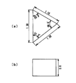
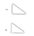
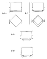
- FIG. 3B is a side view of FIG. 3A. It is a figure which shows the behavior of light. It is a figure which shows the behavior of light. It is a figure which shows the behavior of light. It is a figure which shows the behavior of light. (A) And (b) is a figure which shows the triangle used for the calculation model of light extraction efficiency.
- (A) And (b) is a figure which shows the triangle which reduced the symmetry of the figure used for the calculation model of light extraction efficiency. It is a figure for demonstrating an external light emission profile. It is a figure for demonstrating the farthest side wall part inclined by angle (beta).
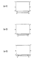
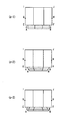
- (A), (b-1), (c-1), and (d-1) are diagrams showing examples in which the shape of the side wall portion, the substrate surface facing the main surface, and the like are variously changed.
- (B-2), (c-2), and (d-2) are diagrams showing examples in which the shape of the side wall portion, the substrate surface facing the main surface, and the like are variously changed.
- (B-3), (c-3), and (d-3) are diagrams showing examples in which the shape of the side wall portion, the substrate surface facing the main surface, and the like are variously changed.
- (E-1), (e-2), and (e-3) are diagrams showing examples in which the shape of the side wall portion, the substrate surface facing the main surface, and the like are variously changed.
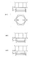
- (A-1), (b-1), (b-2) and (b-3) are diagrams showing examples in which the shape of the side wall portion and the like are variously changed.
- (C-1), (c-2) and (c-3) are views showing examples in which the shape of the side wall portion and the like are variously changed.
- (D-1), (d-2), and (d-3) are diagrams showing examples in which the shape of the side wall and the like is variously changed. It is a figure for demonstrating an integrated type structure.
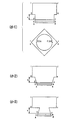
- (A) And (b) is a perspective view which shows the other structural example of the element of this invention. It is a figure for demonstrating the measuring method of curvature.
- (A) And (b) is a figure which shows the substantially triangular shape example by which uneven
- (A) And (b) is the figure which showed the projection shape of the board
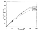
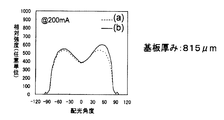
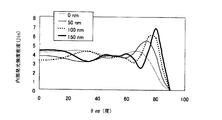
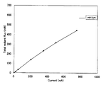
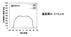
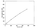
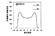
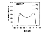
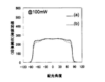
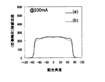
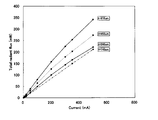
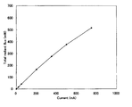
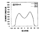
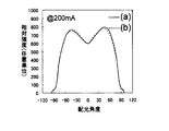
- FIG. 6 is a simulation graph showing an internal light emission profile when the thickness of a second conductivity type semiconductor layer is changed in a range of 150 to 500 nm. It is a figure which shows the measurement result of the total radiant flux of the semiconductor light-emitting device manufactured in Example 2 regarding 1st embodiment of this invention. It is a figure which shows the light distribution characteristic at the time of 200 mA current injection
- FIG. 19A It is a perspective view which shows typically the geometric shape of the semiconductor light-emitting device concerning 2nd embodiment. It is a longitudinal cross-sectional view of FIG. 19A.
- (A) And (b) is a figure which shows the square used for the calculation model of light extraction efficiency.
- (A) And (b) is a figure which shows the unequal square used for the calculation model of light extraction efficiency.
- (A-1), (b-1), (b-2) and (b-3) are diagrams showing examples in which the shape of the side wall portion and the like are variously changed.
- C-1), (c-2) and (c-3) are views showing examples in which the shape of the side wall portion and the like are variously changed.
- (D-1), (d-2) and (d-3) are diagrams showing examples in which the shape of the side wall portion and the like are variously changed. It is a figure for demonstrating an integrated type structure.
- (A) And (b) is a perspective view which shows the other structural example of the element of this invention.
- (A) And (b) is a figure which shows the substantially square shape example by which uneven
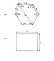
- FIG. 28A It is a perspective view which shows typically the geometric shape of the semiconductor light-emitting device concerning 3rd embodiment. It is a longitudinal cross-sectional view of FIG. 28A.
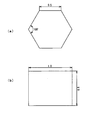
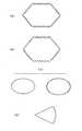
- (A) And (b) is a figure which shows the regular hexagon used for the calculation model of light extraction efficiency.
- (A) And (b) is a figure which shows the hexagon which reduced the symmetry of the figure used for the calculation model of light extraction efficiency.
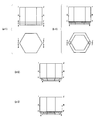
- (A-1), (b-1), (b-2) and (b-3) are diagrams showing examples in which the shape of the side wall portion and the like are variously changed.
- C-1), (c-2) and (c-3) are views showing examples in which the shape of the side wall portion and the like are variously changed.
- (D-1), (d-2) and (d-3) are diagrams showing examples in which the shape of the side wall portion and the like are variously changed. It is a figure for demonstrating an integrated type structure.
- (A) And (b) is a perspective view which shows the other structural example of the element of this invention.
- (A), (b), (c) and (d) is a figure which shows the example of the substantially polygon shape by which uneven
- the planar shape of the substrate is substantially triangular (details will be described later) will be described.
- the gist of the invention is as follows. 1. A nitride substrate whose shape projected in a direction perpendicular to the substrate main surface is substantially triangular; A semiconductor light emitting device having an active layer structure that emits light having a peak emission wavelength ⁇ , and a semiconductor layer portion formed on the main surface of the substrate, wherein the semiconductor light emitting device satisfies formula a1.
- a semiconductor light emitting device comprising: a GaN substrate whose shape projected in a direction perpendicular to the substrate main surface is substantially triangular; and a semiconductor layer portion including an active layer structure and formed on the main surface of the substrate;
- the semiconductor light emitting element characterized by satisfy
- a nitride substrate whose shape projected in a direction perpendicular to the main surface of the substrate is substantially triangular, and a semiconductor layer portion including an active layer structure that emits light having a peak emission wavelength ⁇ and formed on the main surface of the substrate
- a GaN substrate whose shape projected in a direction perpendicular to the main surface of the substrate is substantially triangular;
- a semiconductor light emitting device having an active layer structure and a semiconductor layer portion formed on the main surface of the substrate, wherein the semiconductor light emitting device satisfies formula a7.
- Formula a7 L sc ⁇ 0.418 ⁇ t t ⁇ L sc ⁇ 2.395 (Where t t represents the sum of the maximum physical thickness t s of the substrate and the maximum physical thickness t L of the semiconductor layer portion, and L sc is the longest line segment length formed by any two points on the main surface of the substrate. Represents.)
- the semiconductor light-emitting device according to any one of the above 1 to 4, A semiconductor light-emitting element, wherein the substrate is substantially transparent to light having a peak emission wavelength ⁇ emitted from the active layer structure.
- a refractive index at a wavelength ⁇ of the substrate is n s ( ⁇ ) at a peak wavelength ⁇ of the semiconductor light-emitting device, and a layer constituting the semiconductor layer portion
- the refractive index at the wavelength ⁇ of X is n LX ( ⁇ )
- the semiconductor light emitting element characterized by satisfy
- a main surface of the nitride substrate is a (0001) surface or a surface having an off angle of 5 degrees or less from the surface.
- a main surface of the nitride substrate is a (1-10n) plane or a (11-2n) plane (where n is 0, 1, 2, 3) or a semiconductor light emitting device characterized in that the off angle from these surfaces is 5 ° or less.
- the semiconductor light emitting device wherein the exposed surface of the nitride substrate includes both a surface substantially parallel to the main surface and a surface substantially perpendicular to the main surface. element.
- 21 The semiconductor light-emitting device according to any one of 1 to 20, wherein a planar shape of an end portion of the semiconductor layer portion matches or substantially corresponds to the substantially triangular shape that is a projected shape of the substrate.
- 26 The semiconductor light emitting device as described in 25 above, wherein the thickness of the second conductivity type semiconductor layer is 10 nm or more and 180 nm or less.
- the semiconductor light emitting device according to any one of 30 to 32, wherein the number of the quantum well layers is NUM QW , the average physical thickness of the layers constituting the quantum well layers is T QW (nm), and the quantum wells N QW ( ⁇ ) is the average refractive index of the layers constituting the layer, NUM BR is the number of the barrier layers, T BR is the average physical thickness of the layers constituting the barrier layers, and the barrier layers are The average refractive index of the constituent layers at the wavelength ⁇ is n BR ( ⁇ ), the physical thickness of the second conductive semiconductor layer is T P (nm), and the refractive index of the second conductive semiconductor layer is n P ( ⁇ ).
- the semiconductor light emitting element satisfying the following formula 1
- 35 The semiconductor light emitting device according to any one of 1 to 34, wherein there are a plurality of light emitting units formed in the semiconductor layer portion.
- the semiconductor light-emitting device according to any one of 1 to 40 above, wherein the light-emitting direction is in an arbitrary plane perpendicular to the main surface, and the direction that is a light extraction direction is 0 degrees, and one direction parallel to the main surface Is 90 degrees, the direction opposite to the 90 degree direction is -90 degrees, and when the element is installed in the air and the light distribution characteristics are measured effectively without disturbance, the external emission intensity density
- the direction ⁇ em max indicating the maximum value of the internal light emission intensity density inside the semiconductor light emitting element obtained by using Snell's law from the direction ⁇ em max indicating the maximum value satisfies at least one of the following formulas
- the semiconductor light-emitting device according to any one of 1 to 42 above, wherein the light-emitting direction is in an arbitrary plane perpendicular to the main surface, and the direction as the light extraction direction is 0 degrees, and one direction parallel to the main surface
- the light emitted from the light emitting element is emitted.
- a semiconductor light emitting element characterized in that there is a plane in which the maximum value of the external light emission intensity density is 20% or more larger than the external light emission intensity density at 0 degrees.
- a semiconductor light emitting device comprising the semiconductor light emitting element according to any one of 1 to 43, wherein a semiconductor layer portion side of the semiconductor light emitting element is close to a heat sink.
- a semiconductor light-emitting device comprising the semiconductor light-emitting device according to any one of 1 to 44, wherein the semiconductor light-emitting device is covered with a silicone-based material or a glass material.
- a method for manufacturing a semiconductor light emitting device having a peak light emission wavelength ⁇ in which a shape projected in a direction perpendicular to the main surface of the substrate is substantially triangular, and a nitride substrate having a refractive index at wavelength ⁇ of n s ( ⁇ ) is prepared.
- a first step, a second step of forming a semiconductor layer portion on the main surface of the nitride substrate, a third step of processing the semiconductor layer portion, and the substrate and the processed semiconductor layer portion for each element A method for manufacturing a semiconductor light emitting element, comprising a fourth step of separating, and performing shape processing so as to satisfy formula a1.
- a step, a second step of forming a semiconductor layer portion on the main surface of the GaN substrate, a third step of processing the semiconductor layer portion, and separating the GaN substrate and the processed semiconductor layer portion into each element A method of manufacturing a semiconductor light emitting device, comprising performing a shape process so as to satisfy formula a3.
- a method for manufacturing a semiconductor light emitting device having a peak light emission wavelength ⁇ in which a shape projected in a direction perpendicular to the main surface of the substrate is substantially triangular, and a nitride substrate having a refractive index at wavelength ⁇ of n s ( ⁇ ) is prepared.
- a first step, a second step of forming a semiconductor layer portion having a maximum physical thickness t L on a main surface of the nitride substrate, a third step of processing the semiconductor layer portion, and the substrate and the processed semiconductor A method for manufacturing a semiconductor light emitting device, comprising a fourth step of separating the layer portion into each device, and performing shape processing so as to satisfy only formula a5.
- One step, a second step of forming a semiconductor layer portion having a maximum physical thickness t L on the main surface of the GaN substrate, a third step of processing the semiconductor layer portion, and the processed semiconductor layer with the GaN substrate A method of manufacturing a semiconductor light emitting device, comprising a fourth step of separating the portion into each device, and performing shape processing so as to satisfy only formula a7.
- nitride substrate is a GaN substrate.
- a method for manufacturing a semiconductor light emitting device comprising: performing a substrate exposed surface forming step for forming a substrate, and forming a concavo-convex shape on a substrate for applying a concavo-convex process to at least a part of the substrate exposed surface.
- a substrate thickness adjusting step for adjusting the thickness of the entire substrate, a part of the substrate is processed.
- Manufacturing of a semiconductor light emitting device comprising: performing a substrate exposed surface forming step for forming a new exposed surface; and forming a concavo-convex shape on a substrate for imparting concavo-convex processing to at least a part of the substrate exposed surface.
- the manufacturing method of the semiconductor light-emitting device characterized by the above-mentioned.
- a substrate thickness adjusting step for adjusting the thickness of the entire substrate in the step between the second and third steps, a part of the substrate is processed.
- Manufacturing of a semiconductor light emitting device comprising: performing a substrate exposed surface forming step for forming a new exposed surface; and forming a concavo-convex shape on a substrate for imparting concavo-convex processing to at least a part of the substrate exposed surface.
- 65 A method for manufacturing a semiconductor light emitting device according to any one of the above 46 to 64, wherein the semiconductor layer portion is etched in the third step.
- the manufacturing method of the semiconductor light-emitting element characterized by implementing in either of the depth to.
- 72 The method of manufacturing a semiconductor light emitting device according to any one of 66 to 71, wherein the processing of the end portion of the semiconductor layer portion is any one of dry etching, wet etching, dicing, mechanical scribing, and optical scribing.
- 73 A method of manufacturing a semiconductor light emitting device according to any one of 66 to 72, wherein a planar uneven shape is imparted to an end portion of the semiconductor layer portion.
- 74 A method of manufacturing a semiconductor light emitting device according to 74, wherein a plurality of light emitting units are separated by a light emitting unit separating groove.
- a substrate thickness adjusting step for adjusting the thickness of the entire substrate in the third inter-fourth inter-step process, a part of the substrate is processed.
- Manufacturing of a semiconductor light emitting device comprising: performing a substrate exposed surface forming step for forming a new exposed surface; and forming a concavo-convex shape on a substrate for imparting concavo-convex processing to at least a part of the substrate exposed surface.
- a method of manufacturing a semiconductor light emitting device according to any one of 46 to 77, wherein in the fourth step, a substrate thickness adjusting step for adjusting the thickness of the entire substrate, a part of the substrate is processed, and a new exposed surface is formed.
- a method for manufacturing a semiconductor light emitting device comprising: performing a substrate exposed surface forming step for forming a substrate, and forming a concavo-convex shape on a substrate for applying a concavo-convex process to at least a part of the substrate exposed surface.
- 81. 79. The method for producing a semiconductor light-emitting device according to 79 or 80, wherein the separation starting point is formed by any one of mechanical scribing, optical scribing, dicing, dry etching, and wet etching, or a combination thereof.
- a method for manufacturing a semiconductor light emitting device is any one of mechanical scribing, optical scribing, dicing, dry etching, and wet etching, or a combination thereof.
- a method of manufacturing a semiconductor light emitting device comprising:
- a method of manufacturing a semiconductor light emitting device according to any one of the above 46 to 84, wherein a substrate thickness adjusting step for adjusting the thickness of the entire substrate in a step after the fourth step, a part of the substrate is processed, and a new A method of manufacturing a semiconductor light emitting element, comprising performing at least one of a substrate exposed surface forming step of forming an exposed surface, and a step of forming a concavo-convex shape on a substrate that imparts concavo-convex processing to at least a part of the substrate exposed surface.
- 86 A method of manufacturing a semiconductor light emitting device according to any one of 57, 58, 64, 77, 78, and 85, wherein the substrate thickness adjusting step is performed by any one of polishing and etching, or a combination thereof. A method for manufacturing a semiconductor light emitting device.
- a method of manufacturing a semiconductor light emitting device according to any one of 57, 58, 64, 77, 78, and 85, wherein the substrate exposed surface forming step includes dicing, mechanical scribing, optical scribing, dry etching, and wet.
- the manufacturing method of the semiconductor light-emitting device characterized by implementing by any one method of etching, or these combination.
- a method of manufacturing a semiconductor light emitting device according to any one of 57, 58, 64, 77, 78, and 85, wherein the step of forming a concavo-convex shape on a substrate includes wet etching, dry etching, dicing, mechanical scribing, and optical
- the manufacturing method of the semiconductor light-emitting device characterized by implementing by any one method of scribing, or these combination.
- the semiconductor light-emitting element of the present embodiment is a semiconductor light-emitting element having a semiconductor layer portion on a main surface of a nitride substrate whose shape projected in a direction perpendicular to the main surface of the substrate is substantially triangular.
- the main requirement is that (1) to (3) have a specific relationship.
- Peak emission wavelength ⁇ of a semiconductor light emitting device (2) maximum physical thickness t s or a sum t t of the maximum physical thickness t L of the maximum physical thickness t s and a semiconductor layer portion of the substrate, the substrate (3) The longest line segment length L sc formed by any two points on the substrate main surface
- the substrate thickness with respect to the length of L sc becomes a shape having a substrate having a physical thickness that greatly exceeds the technical common knowledge of those skilled in the art.
- high output and high efficiency can be achieved.
- the main structural requirements of the semiconductor light emitting device of the present invention are supported by a technical idea using the natural law that has been clarified by the present inventors, as will be described later.
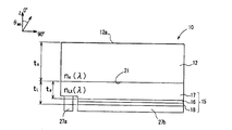
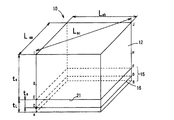
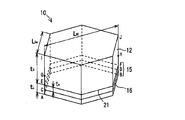
- FIG. 1A shows a semiconductor light-emitting device of one embodiment of the present invention.
- the semiconductor light emitting device 10 of the present invention includes a nitride substrate 12 and a semiconductor layer portion 15 formed on the surface thereof.
- Nitride substrate 12 when a peak emission wavelength of the light emitting element and a lambda, a refractive index of n s (lambda) at the wavelength lambda, the maximum physical thickness of t s.
- the semiconductor layer portion 15 has an active layer structure 16 that can constitute a light emitting element.
- the semiconductor layer portion 15 preferably has one or both of the first conductivity type semiconductor layer 17 and the second conductivity type semiconductor layer 18. Either one or both of the first conductivity type semiconductor layer and the second conductivity type semiconductor layer can arbitrarily include layers having various functions such as a contact layer and a carrier overflow suppression layer.
- the semiconductor light emitting element 10 preferably has a first conductivity type side electrode 27a and a second conductivity type side electrode 27b.
- the substrate surface on which the semiconductor layer portion 15 is formed is expressed as a main surface (see reference numeral 21).
- the Z-axis is taken in a direction perpendicular to the main surface 21, and this direction is set to 0 degrees in the directions of internal light emission and external light emission described later.
- the “side wall portion (side wall surface)” of the semiconductor light emitting element is used when referring to either the substrate side wall portion (side wall surface) or the semiconductor layer side wall portion (side wall surface).
- the “exposed surface” includes a main surface, a substrate surface (12a) facing the main surface, a wall surface, for example, a surface exposed when the substrate is processed, a processed sidewall surface of the semiconductor layer portion 15, and the like.
- the surface used as the boundary with the surrounding medium of a semiconductor light-emitting device is shown.
- a plurality of semiconductor light emitting elements 10 are formed on one substrate during the manufacturing process, and a surface formed by separation from adjacent elements at this time is sometimes referred to as a “separation surface”. As a result, the separation surface may become an exposed surface.
- Exposed surface formation means to form an exposed surface by an arbitrary method and an arbitrary form.
- the nuance for increasing the amount of light entering the critical angle at the interface and increasing the light extraction efficiency is indicated. Sometimes it is used.
- Concavity and convexity processing indicates that irregularities are formed by an arbitrary method and an arbitrary form, and in particular, it may be used with a nuance for increasing the light scattering effect.
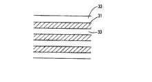
- the active layer structure 16 that the semiconductor light emitting device 10 can optionally have is preferably a quantum well active layer structure having a quantum well layer 31 and a barrier layer 33.
- FIG. 1A shows a structure of a general semiconductor light emitting device.
- the semiconductor light emitting device 10 is provided with a first conductivity type side electrode 27a and a second conductivity type side electrode 27b. Electrons and holes injected from these electrodes 27 a and 27 b are recombined in the active layer structure 16, for example, in the quantum well active layer in the case of a quantum well active layer structure, and light is emitted into the semiconductor light emitting device 10. To do.
- the angular distribution of the emission intensity density in the semiconductor light emitting device 10 strongly depends on the optical interference effect.
- This angular distribution of the light emission intensity density is called an internal light emission profile in the present invention, and is obtained as follows.
- Each quantum well layer portion in the multiple quantum well layer extending in the XY plane direction and substantially parallel to the substrate main surface (21) is assumed to be a planar set of electric dipoles (dipole plane). In the dipole plane, the dipole orientation is uniform in all directions.
- the light emitted from the dipole is multiplexed in each layer of the semiconductor layer portion (multiple quantum well layer portion, second conductivity type side semiconductor layer, second conductivity type side electrode, etc.) and electrode portion in the semiconductor light emitting device 10. Subjected to reflection and multiple interference. As a result, the light emission intensity density J in inside the semiconductor light emitting device 10 is dependent on the radiation direction (the angle between the radiation direction and the Z axis direction is expressed as ⁇ em when the Z axis direction is 0 degree). become.
- the internal light emission profile refers to the dependence of the light emission intensity density (J in ) inside the semiconductor light emitting element on the radiation direction ( ⁇ em ).
- the angle that defines the internal light emitting direction includes an angle (azimuth angle) that the projection of the light emitting direction onto the XY plane makes with the X axis direction, in addition to the angle ⁇ em made with the Z axis direction.
- angle ⁇ em made with the Z axis direction.
- the light emitted from the active layer portion of the semiconductor light emitting device is “isotropic internal light emission profile”, that is, J in is constant in every ⁇ em . Based on the assumption, the invention and the like have been made on the shape and layer structure of the semiconductor light emitting device.
- the internal light emission profile is Can be described as follows.
- I 0 Radiation intensity from dipole r s : Amplitude reflection coefficient in s-polarized electrode surface reflection r p : Amplitude reflection coefficient in p-polarized electrode surface reflection ⁇ : 2 ⁇ nd / ⁇ n: Refractive index at wavelength ⁇ in a region where a dipole surface exists d: Physical distance ⁇ between dipole surface and electrode: Peak wavelength of semiconductor light emitting device.
- multiple reflection and multiple interference between various phases constituting the semiconductor layer portion 15, J in can be calculated using the characteristic matrix method. preferable.
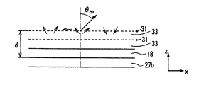
- FIG. 2A shows an example of a model used for obtaining the internal light emission profile of the semiconductor light emitting device of the present invention.
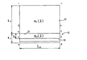
- the active layer structure in the semiconductor light emitting device 10 is a quantum well active layer structure.
- the quantum well layer 31, that is, the dipole surface is present at a distance d from the barrier layer 33 and the second conductivity type semiconductor layer 18 to the second conductivity type side electrode 27b.
- the light emitted from a certain dipole becomes anisotropic due to the interference effect with itself, but the lights emitted from different dipoles do not interfere with each other, and the overall internal emission intensity density Is the sum of the internal emission intensity densities of each anisotropic light.
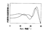
- the direction in which the internal light emission intensity from the dipole in each light emitting layer increases and the direction in which they weaken may cancel each other, but according to the study of the present invention, for example, As a result of having a quantum well active layer structure that satisfies (formula A) to be described later, it always strengthens in a certain direction, that is, a direction close to a direction parallel to the active layer structure. It was found that an internal emission intensity density distribution having a maximum value in the direction of.
- the angle ⁇ em where the horizontal axis is the Z-axis direction and the vertical axis is the internal emission intensity density It becomes a characteristic, that is, an anisotropic internal light emission profile.
- the direction of the maximum value of the internal light emission intensity density varies depending on conditions such as the thickness of the second conductivity type semiconductor layer 18 and the reflectance of the second conductivity type side electrode 27b.
- the direction is close to the direction parallel to the structure (the direction in which ⁇ em is close to 90 °).
- Such a tendency that the internal emission intensity density increases in a direction nearly parallel to the active layer structure becomes more conspicuous in, for example, a light-emitting element having a quantum well active layer structure that satisfies (Formula A) described later.
- FIG. 2B shows that the internal emission profile from dipole radiation with an isotropic orientation becomes essentially anisotropic. That is, when it is assumed that an appropriate refractive index difference exists between the quantum well layer, the barrier layer, and the second conductivity type semiconductor layer 18 and the light emitting layer has an appropriate thickness, the following natural law is used. Is obtained. “When there is a moderate difference in refractive index between the quantum well layer, the barrier layer, and the second conductivity type semiconductor layer 18, for example, when the quantum well active layer structure satisfies the following (formula A), isotropic Dipolar radiation with a specific orientation results in an anisotropic internal emission profile, and the internal emission intensity density increases in a direction near the active layer structure. "formula A)
- Isotropic orientation when it is assumed that there is an excessive refractive index difference between the quantum well layer, the barrier layer, and the second conductivity type semiconductor layer 18 or the light emitting layer has an excessive thickness
- the refractive index difference increases beyond an appropriate range, or when the light emitting layer exceeds the appropriate range and is thick, the degree is as shown in FIG. 2C (a) and (b).
- the refractive index difference between the quantum well layer, the barrier layer, and the second conductivity type semiconductor layer 18 increases, the light emitted in the direction close to the parallel to the active layer structure is reflected more strongly, resulting in multiple reflection. It is absorbed by an electrode with finite reflectivity. Further, when the thickness of the light emitting layer is increased, light emitted in a direction nearly parallel to the active layer structure is canceled out in the sum of light emission from the respective dipoles. As a result, it is assumed that the refractive index difference between the quantum well layer, the barrier layer, and the second conductivity type semiconductor layer 18 is larger than an appropriate range, or the light emitting layer has an excessive thickness. If you get the following natural law:
- Isotropic when the difference in refractive index between the quantum well layer, the barrier layer, and the second conductivity type semiconductor layer 18 increases beyond an appropriate range, or when the light emitting layer has an excessive thickness, etc. Dipole radiation with a common orientation results in an isotropic internal emission profile.
- the semiconductor light-emitting element of the present invention has an appropriate refractive index difference between the quantum well layer, the barrier layer, and the second conductivity type semiconductor layer 18. Or the case where a light emitting layer has moderate thickness etc. is preferable.
- the active layer structure preferably has a quantum well active layer structure, whereby an internal light emission profile can be realized that is anisotropic with a maximum value of internal light emission intensity density in a direction parallel to the active layer structure.
- such an active layer structure can be realized, for example, by appropriately selecting a difference in refractive index between the quantum well layer and the barrier layer.
- it can be realized by appropriately selecting the number of repetitions of the quantum well layer and the barrier layer, or appropriately selecting the thicknesses of the quantum well layer and the barrier layer.
- NUM QW represents the number of quantum well layers included in the active layer structure
- T QW (nm) represents the average physical thickness of the layers constituting the quantum well layer
- NUM BR represents the number of barrier layers included in the active layer structure
- T BR (nm) represents the average physical thickness of the layers constituting the barrier layer
- T P (nm) represents the physical thickness of the second conductivity type semiconductor layer
- n QW ( ⁇ ) represents the average refractive index at the wavelength ⁇ of the layers constituting the quantum well layer
- n BR ( ⁇ ) represents an average refractive index at a wavelength ⁇ of a layer constituting the barrier layer
- n P ( ⁇ ) represents the average refractive index of the second conductivity type semiconductor layer at the wavelength ⁇
- n s ( ⁇ ) represents the refractive index at the wavelength ⁇ of the substrate as described above.
- the number of quantum well layers is preferably 4 or more and 30 or less.
- the maximum value of the thickness of the quantum well layer included in the active layer structure is 40 nm or less.
- the present application also discloses a semiconductor light emitting device having an anisotropic internal light emission profile, in which the quantum well active layer satisfies the above formula.
- the present invention can be independently configured without combining with other configurations disclosed in the present application. It can also be combined with other configurations disclosed in the present application.
- the semiconductor light emitting device of the present invention is anisotropic in the internal light emission profile as shown in the graphs (a) to (c) of FIG. 2B or FIG.
- the maximum value of the intensity density has a characteristic close to the direction parallel to the active layer structure. That is, it is preferable that the emission intensity density distribution with respect to the internal emission direction ( ⁇ em ) of the semiconductor light emitting device of the present invention is not isotropic.
- the direction ( ⁇ em max ) having the maximum value is a direction close to the parallel direction of the active layer structure.
- the direction ( ⁇ em max ) giving the maximum value of internal light emission varies depending on the material constituting the semiconductor layer portion, the structure of each layer, the electrode material, and the structure thereof.
- the direction ( ⁇ em max ) giving the maximum value of internal light emission includes the first conductivity type semiconductor layer constituting the semiconductor layer portion, the active layer structure including the quantum well active layer and the barrier layer, and the second conductivity type. It varies depending on the semiconductor layer, the contact layer, various structures that can be arbitrarily introduced, the constituent material of the first conductivity type side electrode, the constituent material of the second conductivity type side electrode, the structure thereof, and the like.
- ⁇ em max can be most strongly changed by the reflection effect due to the difference in refractive index between the quantum well layer, the barrier layer, and the second conductivity type semiconductor layer 18 and the different bipolar from the light emitting layer having a certain thickness. This is an effect of canceling anisotropy as a result of the addition of light emission by the child.
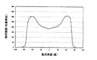
- ⁇ em max is It can be changed in the range of 67.5 degrees ⁇ ⁇ em max ⁇ 90 degrees. This is simultaneously ⁇ 90 degrees ⁇ em max ⁇ ⁇ 67.5 degrees.
- the present inventors have found the following. That is, it is more effective to extract the light emitted in such a direction from the side wall surface than to extract from the “upper surface (the substrate surface 12 a facing the main surface in FIG. 1A)” of the semiconductor light emitting element 10.
- the angle ( ⁇ em max ) indicating the maximum value of the internal light emission intensity density emitted from the active layer structure 16 of the semiconductor light emitting device 10 to the inside of the semiconductor light emitting device has a lower limit of the absolute value of 67.5 degrees or more. It is preferably 70.0 degrees or more, more preferably 72.5 degrees or more, and further preferably 75.0 degrees or more.
- the upper limit of the absolute value of ⁇ em max is preferably smaller than 90 degrees, more preferably 87.5 degrees or less, more preferably 85.0 degrees or less, and 82.5 degrees or less. More preferably it is.
- light mainly extracted from the side surface of the light emitting device is mainly light in the direction in which the light is emitted at a high density internally. It is an essential and effective method for improving efficiency. This is a conclusion that cannot be reached from the isotropic internal light emission profile disclosed heretofore.
- the active layer structure has a quantum well structure and the refractive index difference between the quantum well layer and the barrier layer is small within an appropriate range
- the light emitted internally from the active layer structure 16 is 67.5 degrees ⁇ Since ⁇ em max ⁇ 90 degrees, the side wall of the semiconductor light emitting element 10 can be reached.
- the refractive index difference at the interface of the semiconductor layer constituting the active layer structure 16 and the other semiconductor layer portion is small in an appropriate range
- the refractive index difference at the interface between the semiconductor layer portion and the nitride substrate is also in an appropriate range. The same is true for small cases. Therefore, it is most effective to extract the light emitted internally from the active layer structure 16 from here.
- the present application is a semiconductor light emitting device having an anisotropic internal light emission profile, and the absolute value of the angle ⁇ em max indicating the maximum value of the internal light emission intensity density is 67.
- a semiconductor light emitting device satisfying 5 degrees or more and less than 90 degrees is also disclosed, and the invention can be independently configured without combining with other structures disclosed in the present application. It can also be combined with other configurations disclosed in the present application.
- the external light emission profile that is, the light distribution characteristic is determined according to Snell's law as a comprehensive result of reflection, transmission, refraction, and the like of light at the interface between the internal light emission profile and the peripheral medium of the semiconductor light emitting element.
- the external light emission profile is a distribution of the emission intensity density (J out ) outside the semiconductor light emitting element with respect to the radiation direction ( ⁇ em ). That is, ⁇ em max cannot be observed directly, but by observing the ( ⁇ em max ) direction indicating the maximum value of the emission intensity density (J out ) outside the semiconductor light emitting element, It is possible to obtain by calculating backward from the law of.
- the light distribution characteristics are measured in the air by mounting the light emitting elements on a stem or the like that eliminates the portion that can be a reflecting mirror as much as possible. It is preferable to do.
- the present inventors take out the internal light emitted in the other direction including the direction having the maximum value of the above-mentioned internal light emission intensity density as much as possible from the side wall of the semiconductor. Has been found to be effective in improving the light extraction efficiency of the semiconductor light emitting device. That is, the semiconductor light emitting device of the present invention is characterized in that the shape of the nitride substrate projected in the direction perpendicular to the main surface of the substrate is substantially triangular. In addition, one of the features is that a specific relationship is satisfied between the longest line segment length formed by any two points on the substrate main surface and the maximum physical thickness of the nitride substrate.
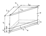
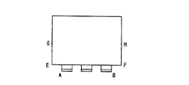
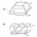
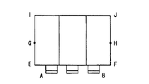
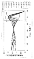
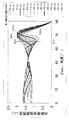
- FIG. 3A is a perspective view schematically showing the geometric shape of the semiconductor light emitting device.
- the semiconductor light emitting device 10 includes a semiconductor layer portion 15 including an active layer structure 16 that emits light having a peak emission wavelength ⁇ on the main surface (the lower side of the drawing) of the nitride substrate 12. is doing.
- the nitride substrate 12 when the nitride substrate 12 is projected onto the main surface 21 in the vertical direction, it has a substantially triangular shape. Further, since all of the side wall surfaces are perpendicular to the main surface 21, the projected shape of the nitride substrate 12 matches the planar shape of the main surface 21, and the main surface also has a substantially triangular shape.
- the shape projected in the vertical direction on the main surface of the substrate generally matches the shape of the adjacent element isolation end.
- the planar shape of the main surface 21 is smaller than the shape of the substrate projected perpendicularly to the substrate main surface.
- the main surface shape of the substrate may be substantially triangular (however, smaller than the shape in which the substrate is projected in the vertical direction on the main surface of the substrate). 4 or a natural number of 100 or less), a circular shape, an elliptical shape, an indefinite shape surrounded by a curve, an indefinite shape surrounded by a straight line and a curve, or the like.
- the longest line segment length formed by any two points on the main surface of the substrate is L sc
- the refractive index at the wavelength ⁇ of the substrate is n s ( ⁇ ).
- the maximum physical thickness t s of the substrate satisfies the following equation a1.
- the configuration satisfying these equations can effectively improve the light extraction efficiency from the side wall of the semiconductor light emitting device in which the direction of the maximum value of the internal light emission intensity density is close to the parallel direction to the active layer structure.
- such a structure can be realized by a simple manufacturing method. Further, such a structure is advantageous in that the light distribution characteristic can be controlled.
- all of the side wall surfaces are perpendicular to the main surface 21, and the projection shape of the nitride substrate 12 matches the planar shape of the main surface 21. It is also an end shape.
- the projected shape is a substantially triangular shape, the shape is superior to that of a pentagonal or more polygonal structure, and the surface filling property is superior, which is advantageous when a large number of semiconductor light emitting devices are formed on a nitride substrate.
- the square planar shape can be formed by scribing from two orthogonal directions, but to form a triangular planar structure, it is only necessary to add scribe formation from one direction. It can be taken out from the nitride substrate.
- the fact that a large number of semiconductor light-emitting elements can be taken out from the nitride substrate means that the semiconductor light-emitting element of the present invention having a shape having a substrate having a physical thickness that greatly exceeds the technical common sense of those skilled in the art. It is also extremely effective from the viewpoint of effective use of the nitride substrate and cost reduction.
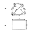
- a triangular planar structure that can be formed by scribing from three directions, at least one of the three sides can be designed to have a side with a different length from the other side. Triangular shapes can be designed for control purposes. Such a design is particularly effective in the present invention which is characterized in that light emitted into the semiconductor light emitting element is extracted from the side wall surface.
- the proportion of vertices whose angles are acute among all vertices can be easily increased compared to other figures.
- all corners are acute angles, but there are no acute angles in squares, regular pentagons, and regular hexagons.
- the two angles are acute angles, so the ratio of the acute angles is 2/3 or more.
- the acute angle part forms a planar shape that is advantageous in extracting light emitted in the vicinity of the acute angle part. Therefore, in the semiconductor light emitting device of the present invention mainly focusing on light extraction from the side wall surface. It is particularly preferable that the shape projected in the vertical direction on the main surface of the substrate is a substantially triangular shape.
- the projection shape of the semiconductor light emitting element is selected to be a triangle
- a shape having low symmetry is preferable because it is advantageous for light extraction.
- an isosceles triangle is more preferable than an equilateral triangle, and an unequal triangle having different lengths and angles of all sides is advantageous for light extraction. This is because in the case of a highly symmetric figure, planar stay light is generated due to the symmetry. On the other hand, when the symmetry is low, such staying light is unlikely to occur. This “symmetry” will be supplemented with “H: symmetry” in the latter half of this specification.
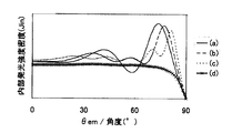
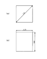
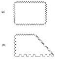
- FIG. 3F and FIG. 3G respectively show the case where the shape projected from the vertical direction on the main surface of the substrate is an equilateral triangle in the semiconductor light emitting device in which the substrate portion is surrounded by an optically flat surface, and the symmetry of the figure is lowered.
- a model for calculating the light extraction efficiency is shown. As a result, it has been confirmed that the light extraction efficiency of the inequilateral triangle is 1.4 times that of the regular triangle.
- the projection shape is a triangle
- a shape with low symmetry is preferable because it is advantageous for light extraction.
- This is preferable in a semiconductor light-emitting device that mainly emits light from the side surface as in the present invention, and has a remarkable synergistic effect.
- the light extraction efficiency from the side wall surface is synergistically improved in combination with the increase in the physical thickness of the substrate described above, and a remarkable effect that cannot be predicted by those skilled in the art can be realized.
- the combination of the physical thickness of the substrate and the projected shape has great technical significance.
- the shape of the substrate projected from the direction perpendicular to the main surface is substantially triangular.
- substantially triangular refers to a figure (triangle) surrounded by three sides, such as a regular triangle, an isosceles triangle, and an unequal triangle, and generally has a triangular shape, but the three sides are strictly straight lines. Instead, it is intended that a part of or all of one or more sides may have a fine corrugated shape or irregular shape regularly or irregularly.
- the shape of the fine unevenness is, for example, as described later in the section ⁇ Substrate surface orientation and unevenness formation on the substrate>, the unevenness size (height difference from the line) is the peak wavelength of the semiconductor light emitting element ⁇ Can have dimensions of about ⁇ / 50 to 50 ⁇ . Preferably, it has a dimension of about ⁇ / 10 to 10 ⁇ , more preferably a dimension of about ⁇ / 7 to 7 ⁇ , and more preferably a dimension of about ⁇ / 5 to 5 ⁇ .
- the distance between the concave portions adjacent to the concave portion can have a dimension of about ⁇ / 50 to 50 ⁇ , where ⁇ is the peak wavelength of the semiconductor light emitting element.
- ⁇ is the peak wavelength of the semiconductor light emitting element.
- it has a dimension of about ⁇ / 10 to 10 ⁇ , more preferably a dimension of about ⁇ / 7 to 7 ⁇ , and more preferably a dimension of about ⁇ / 5 to 5 ⁇ .
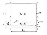
- the refractive index at the wavelength ⁇ of the surrounding medium is expressed as n out ( ⁇ )
- the refractive index at wavelength ⁇ of the nitride substrate is expressed as n s ( ⁇ )
- t s be the physical thickness of the thickest part of the substrate
- the refractive index at the wavelength ⁇ of the layer X constituting the semiconductor layer portion is represented by n LX ( ⁇ ) (that is, the layer X represents an arbitrary layer constituting the semiconductor layer portion, and n LX ( ⁇ ) is the wavelength of the layer X. represents the refractive index at ⁇ ).
- the maximum physical thickness from the substrate main surface to the active layer structure is t a
- Let t L be the maximum physical thickness of the semiconductor layer portion.
- the longest line segment length (straight line length) formed by any two points on the main surface of the substrate is L sc .
- the length of the shortest side of the substantially triangular shape of the main surface of the substrate is L sa .
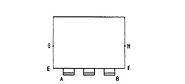
- points A and B are points at the end of the semiconductor layer portion 15 (the lower side of the figure).
- Points C and D are end points of the active layer structure 16.
- Points E and F are points at the end of the boundary between the main surface 21 and the semiconductor layer portion 15.
- Point G and point H are points where the element is separated from other semiconductor light emitting elements 10 adjacent to each other in manufacturing (in this shape, the other points are also the ends where the elements are separated). is there.
- Point I and point J are points at the end of the substrate on the surface opposite to the main surface 21 (upper side in the figure).
- the maximum value of the internal emission intensity density of light emitted from the active layer structure 16 (the maximum value of the internal profile) is relatively close to the parallel direction of the active layer structure.
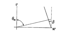
- the light emitted from the point C in FIG. 3A is assumed, and this includes the direction of the maximum value of the internal emission intensity density and includes the point C as much as possible. Assuming internal light emission radiated in the other direction from the semiconductor light emitting device shape in which these lights can be effectively extracted from the wall portion (the farthest side wall portion) of the light emitting device farthest from the point C You can do it.
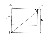
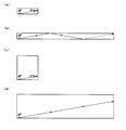
- FIG. 3B is a view of the surface surrounded by the symbol IABJ of the element of FIG. 3A viewed from the vertical direction.
- FIG. 3B a straight line including point A to point I, a straight line including point B to point J (farthest side wall portion), and a plane surrounded by point A, point B, and point I, point J are illustrated.
- the distance between the points A and B is the longest line segment length L sc formed by any two points on the main surface of the substrate, and in this case, corresponds to the longest side (see FIG. 3A).
- n s ( ⁇ ) and n LX ( ⁇ ) do not differ greatly, light generated from the active layer structure sufficiently reaches the side surface of the nitride substrate.
- the maximum physical thickness t a from the main surface 21 to the active layer structure is sufficiently thin compared to the thickness t s of the nitride substrate. Therefore, assuming that the light emission from the point C is the light emission from the point E, the critical angle in the farthest side wall portion including the point B point D point F point H point J may be considered.
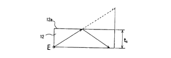
- FIG. 3C is a diagram showing the behavior of light.
- the farthest side wall (the right wall in the figure) is divided into the following three regions 131, 132, and 133 corresponding to the behavior of light.
- the first is the lowermost region 131 of the farthest side wall.
- n out ( ⁇ ) is the refractive index of the peripheral medium at the emission wavelength ⁇ of the semiconductor light emitting element.
- the second is an area 132 existing on the above-described area 131.
- - ⁇ c The second region of the farthest side wall with respect to the point E, or the intrinsic confinement light generation region).
- the third is a region 133 further above the region 132 described above.
- the light incident on the first region 131 on the farthest side wall is not totally reflected. Therefore, light can be effectively extracted from the first region 131 in the farthest side wall portion.
- light incident on the second region 132 on the farthest side wall and light incident on the third region 133 on the farthest side wall are subjected to total reflection.
- the second region 132 of the farthest side wall portion is a region where even if the light that has undergone total reflection is reflected and reaches the other light emitting element side wall surface, it is further subjected to total reflection on that surface. In other words, it is a region that creates “intrinsic confinement light” in the semiconductor light emitting device.
- the light incident on the third region 133 is totally reflected at the farthest side wall, but has an incident angle smaller than the critical angle at the other part (for example, the substrate surface 21a), so that it can be taken out by repeating the reflection. .
- the thickness t s (FIG. 3B) of the nitride substrate 12 is thin so as to be within the first region 131 of the farthest side wall portion, as shown in FIG.
- Light that can be extracted from the farthest side wall portion if there is a thickness is totally reflected by the substrate surface 12a facing the main surface, and is absorbed when the light is incident on the active layer structure again, or Since it may be absorbed by the second conductivity type side electrode, the first conductivity type side electrode, etc., it is not preferable.
- the reflectivity of the electrode or the like is 100% and the loss of the nitride substrate and the semiconductor layer portion is 0, the light can be emitted from the side wall by repeating multiple reflection. Environment is not realized. That is, the thickness t s of the nitride substrate may such that the first region 131 is not preferable from the viewpoint of efficient extraction of light.
- the thickness t s of the preferred nitride substrate in the present invention is given as follows.
- the intensity of light emitted internally from the active layer structure has its maximum value in a direction relatively close to the direction parallel to the active layer structure 16
- light in a direction with a high internal emission intensity density is converted into a semiconductor.
- the thickness t s of the nitride substrate first The thickness is within the two regions (intrinsic confinement light generation region) 132.
- the thickness t s of the nitride substrate in the present invention is preferably more than the thickness (t 1 in FIG. 3C) the lower limit of the thickness of the intrinsic confinement light generation region 132.
- the upper limit of the thickness t s is preferably less 5500 ⁇ m in terms of isolation.
- thickness t s of the nitride substrate is preferably to a thickness of at least the thickness of the lower limit of the intrinsic confinement light generation region 132 (t 1 in the figure), the upper limit of the intrinsic confinement light generation region thickness (in FIG. t 2 ) More preferably, the thickness is less than or equal to. That is, the thickness t s of the nitride substrate, the thickness of the intrinsic confining light generation region, i.e., t 1 ⁇ t s ⁇ t 2 More preferably.
- the thickness t s of the nitride substrate of the present invention the aspect ratio of the longest line segment lengths to make the two arbitrary points overlaying the substrate main surface and L sc (t s / L sc )
- tan ⁇ t s / L sc tan ⁇ sin ⁇ 1 (n out ( ⁇ ) / n s ( ⁇ )) ⁇ ⁇ t s / L sc ⁇ tan ⁇ 90 ⁇ sin ⁇ 1 (n out ( ⁇ ) / n s ( ⁇ )) ⁇ It is.
- t s of the nitride substrate 12 of the semiconductor light-emitting device 10 of the present invention L sc ⁇ tan ⁇ sin ⁇ 1 (n out ( ⁇ ) / n s ( ⁇ )) ⁇ ⁇ t s ⁇ L sc ⁇ tan ⁇ 90 ⁇ sin ⁇ 1 (n out ( ⁇ ) / n s ( ⁇ )) ⁇ (formula a1a) It becomes.
- n out ( ⁇ ) can be set to 1 assuming vacuum or effectively air. Therefore, the preferred substrate thickness of the semiconductor light emitting device in the present invention is: L sc ⁇ tan ⁇ sin ⁇ 1 (1 / n s ( ⁇ )) ⁇ ⁇ t s ⁇ L sc ⁇ tan ⁇ 90 ⁇ sin ⁇ 1 (1 / n s ( ⁇ )) ⁇ (formula a1) It becomes.
- the thickness t s of the nitride substrate in the present invention as described below, the maximum thickness length extended from the main surface vertically thickest.
- the substrate thickness preferably satisfies the formula a1, and the light emitted in the direction giving the maximum value of the internal light emission intensity density directly enters the farthest side wall portion within the specified thickness. Further, from the viewpoint of manufacturing cost and the like, it is advantageous that the thickness of the substrate is set to the minimum necessary thickness while satisfying these.
- the index that can be the lower limit of the thickness t s of the semiconductor light-emitting device of the present invention (A) L sc ⁇ tan ⁇ sin ⁇ 1 (1 / n s ( ⁇ )) ⁇ (B) L sc ⁇ tan ⁇ 1 ⁇ (90 ⁇ em max ) ⁇ (C) L sc ⁇ tan ⁇ 1.5 ⁇ (90 ⁇ em max ) ⁇ (D) L sc ⁇ tan ⁇ 2.0 ⁇ (90 ⁇ em max ) ⁇ It is.
- (A) is an index defined by the critical angle of light emitted from the point E in the farthest side wall, and is a necessary requirement to be satisfied by the present invention.
- the preferable range in the present invention is 67.5 degrees ⁇ ⁇
- em max ⁇ 90.0 degrees, here, 45 degrees ⁇ em max ⁇ 90 degrees is sufficient as a mathematical range, and after satisfying the requirement of (a), which may give preferable lower limit of the thickness t s to the semiconductor light-emitting device satisfies.
- the semiconductor light emitting element of the present invention may give a preferable lower limit value of the thickness to be satisfied.
- the index that can be the preferred upper limit of the thickness t s of the semiconductor light-emitting device of the present invention L sc ⁇ tan ⁇ 90-sin ⁇ 1 (1 / n s ( ⁇ )) ⁇ (F) 2.5 ⁇ L sc ⁇ tan ⁇ sin ⁇ 1 (1 / n s ( ⁇ )) ⁇ (G) 2.0 ⁇ L sc ⁇ tan ⁇ sin ⁇ 1 (1 / n s ( ⁇ )) ⁇ (H) 1.5 ⁇ L sc ⁇ tan ⁇ sin ⁇ 1 (1 / n s ( ⁇ )) ⁇ It is.
- (E) is an index defined by the critical angle of light emitted from the point E in the farthest side wall, and is a requirement that the present invention preferably satisfies.
- (F) to (h) are more preferable indicators of the substrate thickness that can be provided so that the substrate thickness is the minimum necessary thickness.
- the semiconductor light emitting device of the present invention which may give a preferred upper limit of the thickness t s to the substrate inherent satisfies.
- (f) means that the thickness of the substrate is preferably within 2.5 times the minimum necessary thickness, (g) is within 2 times, and (h) is preferably within 1.5 times. .
- n s ( ⁇ ) increases as the wavelength becomes shorter, but it is necessary to select n s ( ⁇ ) within a range where absorption is not large. Further, in the nitride substrate 12, for example, even if an AlN substrate, a BN substrate, or the like is assumed, the refractive index at the same wavelength is smaller than that of the GaN substrate.
- n s ( ⁇ ) would give a thickness t s of the widest range of the nitride substrate may have a 2.596 from the measured value at 370nm of the GaN substrate.
- the lower limit of the thickness of the semiconductor light-emitting device of the present invention is L sc ⁇ 0.418 ⁇ t s And more preferably, L sc ⁇ 0.577 ⁇ t s It is.
- the upper limit of the thickness t s of the semiconductor light-emitting device of the present invention is t s ⁇ L sc ⁇ 2.395 It is preferable that t s ⁇ L sc ⁇ 1.045 More preferably, t s ⁇ L sc ⁇ 0.836 More preferably, t s ⁇ L sc ⁇ 0.627 Most preferably.
- the expression a3 is L sc ⁇ 0.450 ⁇ t s ⁇ L sc ⁇ 2.221 Then, the range becomes narrower than the expression a3.
- Table 1 shows a GaN substrate (“C-GaN” in the table) whose main surface is the (0001) plane and a GaN substrate (“m-GaN” in the table) whose main surface is (1-100). ) Shows the result of actual measurement of the refractive index.
- the second region 132 farthest side wall portion of the E points defining the thickness t s of the nitride substrate (intrinsic confinement light generation region) will not be present.
- the internal light emission profile is anisotropic and ⁇ em max, which is the direction giving the maximum value of the light emission intensity density, is 67.5 degrees ⁇ ⁇ em max ⁇ 90 degrees. Therefore, it is preferable that light extraction from the farthest side wall portion is easily realized.
- Formula a1a is a peripheral medium of the semiconductor light emitting device of the present invention.
- n out ( ⁇ ) ⁇ n s ( ⁇ ) is an element placed in a peripheral medium where 45 degrees ⁇ sin ⁇ 1 (n out ( ⁇ ) / n s ( ⁇ )) ⁇ 90 degrees.
- n out ( ⁇ ) is assumed small n s (lambda) is large, it is possible to obtain the thickness t s of the broadest scope of the preferred nitride substrate. This is because even if the refractive index of the GaN substrate is a value of about 2.43 at about 460 nm, the refractive index of the peripheral medium is a practical limit of about 2.20 or less.
- n out (lambda) is the vacuum or effectively assume air, giving a thickness t s widest range of the nitride substrate obtained by this with 1 .
- the semiconductor light-emitting element of the present invention is a light-emitting element on the formula a1 or a GaN substrate. If Expression a3 is satisfied, sufficient light extraction from the side wall is possible.
- indices for giving a preferable substrate thickness are as shown in (a) to (h).
- the thickness of the second conductivity type semiconductor layer that can be a main component between the point C and the point A is sufficiently smaller than the thickness of the entire layer constituting the other semiconductor layer portion. It is also possible to approximate the s + t a as t s + t L. That is, the end of the active layer structure can be approximated to the end of the semiconductor layer portion.
- the point C is a light emitting point without making such approximations, but the structure of the semiconductor layer, particularly the light emitting part when using the quantum well active layer structure is not necessarily specified. Since it is not easy, it is a realistic guideline and preferable to satisfy the approximate expressions of expressions a1, a3, a5, and a7.
- L sa and L sc The length of a normal GaN-based semiconductor light-emitting element L sa and L sc is about 250 [mu] m, t s is about 100 [mu] m. Furthermore, L sa and L t s even large chip that is longer than about 1mm of sc is approximately 100 [mu] m.
- the substrate that has been mainly used is an excessively hard material such as sapphire, and its thickness is mainly determined by the convenience of element separation process of element separation and dicing.
- a GaN-based semiconductor light emitting device on a different substrate such as sapphire has a problem of thermal distortion when a semiconductor layer portion is formed on the substrate, and crystal growth is difficult on a substrate having a thickness of about 100 ⁇ m. Therefore, it is necessary to form a semiconductor layer 15 with a substrate thickness exceeding 400 ⁇ m, and then polish the substrate to a thickness of about 100 ⁇ m at the final stage of the device fabrication process to prepare for the device isolation step. The process was complicated.
- a nitride substrate such as a GaN substrate
- its hardness is lower than that of a sapphire substrate, and element separation processes such as scribing, breaking, and dicing are relatively easy even with a relatively thick substrate. it can.
- its hardness is harder than GaAs, GaP, InP, ZnO, etc., and it is not as easy as these materials in element isolation processes such as scribe, braking, dicing and the like. That is, when using a nitride substrate, it is necessary to overcome special circumstances due to its hardness.
- problems such as thermal distortion will be reduced.
- the handling of the process is easy, and the preferable lower limit of the thickness t s of the GaN substrate of the semiconductor light emitting element capable of forming a high-quality semiconductor layer portion, was at 250 ⁇ m thickness .
- a semiconductor light emitting device having a substrate having a thickness of 250 ⁇ m was easily isolated by various methods such as scribing, breaking, and dicing, and L sa that can be converted into a device was experimentally determined.
- element separation was easy when L sa was 250 ⁇ m or more.
- the thickness is 400 ⁇ m or more, the occurrence of damage to the element itself and the yield reduction due to this are reduced.
- L sa is 550 ⁇ m or more, the occurrence of chipping or the like due to the braking process is particularly reduced.
- chipping in the chip outer shape is described as follows. Suppressing the occurrence has great technical significance.
- the angle of the two vertices is an acute angle at least among the vertices, so the ratio of the acute angle is 2/3 or more.
- the acute angle portion forms a planar shape that is advantageous for light extraction as compared with the obtuse angle portion. Therefore, in the semiconductor light emitting device of the present invention mainly for light extraction from the side wall surface, the direction perpendicular to the substrate main surface. It is particularly preferable that the shape projected on the surface is a substantially triangular shape. However, since the acute angle portion is easily chipped, it is technically significant to suppress this chipping.
- the lower limit of L sa when ts is relatively thin is preferably 250 ⁇ m or more, more preferably 400 ⁇ m or more, and more preferably 550 ⁇ m or more.
- the L sc When dicing was performed so as to have a thickness of 5000 ⁇ m or less, when the device was peeled from the sheet after dicing, excessive damage was not induced in the device, and the yield reduction was reduced.
- L sc 2000 ⁇ m or less
- the degree of breakage of the element was further reduced, and many elements having a favorable shape were preferred.
- L sc was 1550 ⁇ m or less, extremely good element isolation was possible.
- the upper limit of L sc where t s is relatively thick there generally below 5000 .mu.m, preferably not more than 2500 [mu] m, more preferably equal to or less than 2000 .mu.m, more preferably was less than 1550.
- the semiconductor light emitting element 10 having a planar shape satisfying 550 ⁇ m ⁇ L sa ⁇ L sc is a semiconductor light emitting element in a category called a so-called large chip.
- a large chip has a problem that its light emission efficiency is low, but according to the light emitting element of the present invention, light can be efficiently extracted from the side wall of the semiconductor light emitting element.
- the L sc is about 778 ⁇ m
- the substrate thickness required from the formula a3 is about the lower limit. 325 ⁇ m.
- the semiconductor light emitting device of the present invention is a very effective method for a large chip, which has a problem of low luminous efficiency.
- the planar shape is a triangle, it is advantageous to extract light from an acute angle portion. Therefore, light extraction efficiency superior to other shapes is expected.
- the semiconductor light emitting device of the present invention is polished after forming a high-quality semiconductor layer portion on the prepared nitride substrate. Even if this process is not carried out, the shape can be produced by a simple method. Further, since the light distribution characteristic can be controlled, a large-sized semiconductor light-emitting element having favorable characteristics can be manufactured at low cost.
- the semiconductor light emitting device 10 on a nitride substrate having a planar shape satisfying 550 ⁇ m ⁇ L sa ⁇ L sc ⁇ 1550 ⁇ m is further preferable, and it is possible to perform remarkably easy and good device isolation.
- the lower limit of the above formula is more preferable when satisfying 650 ⁇ m or more, more preferable when satisfying 800 ⁇ m or more, more preferable when satisfying 850 ⁇ m or more, and most preferable when satisfying 900 ⁇ m or more.
- the upper limit of the above formula is more preferably 1450 ⁇ m or less, more preferably 1300 ⁇ m or less, further preferably 1250 ⁇ m or less, and most preferably 1200 ⁇ m or less.
- a semiconductor light-emitting device having a planar shape satisfying L sa ⁇ L sc ⁇ 550 ⁇ m that is, a so-called small chip
- L sa ⁇ L sc ⁇ 550 ⁇ m that is, a so-called small chip
- these elements mainly extract light from the side wall, they are highly efficient and can control light distribution characteristics. Therefore, the present invention is very effective even when L sa ⁇ L sc ⁇ 550 ⁇ m, and it is also preferable to have such a planar size.
- the present invention is a technique that can be suitably used for semiconductor light-emitting elements in the purple, near-ultraviolet, and ultraviolet regions, which generally do not have high reflectivity at electrodes.
- the lower limit of the peak emission wavelength ⁇ is preferably 370 nm or more, more preferably 380 nm or more, more preferably 390 nm or more, and more preferably 400 nm or more. Furthermore, the upper limit of the peak emission wavelength ⁇ is preferably 430 nm or less, more preferably 420 nm or less, and more preferably 410 nm or less.
- the nitride semiconductor for setting the light emitted from the active layer structure 16 in the above range includes a quantum well layer made of In x Ga 1-x N and a barrier layer made of Al y Ga 1-y N.
- a quantum well active layer structure can be exemplified, but in this, when realizing the above wavelength range, it is possible to easily realize a configuration for reducing the refractive index difference between the quantum well layer and the barrier layer, and There are configurations that can confine enough electron-hole pairs.
- the In x Ga 1-x N-based quantum well layer capable of realizing such a wavelength can have an In composition x of about 0.10 or less when a GaN substrate is used, for example.
- the barrier layer can be made of GaN, which is preferable because the difference in refractive index is reasonably small.
- the barrier layer 33 (see FIG. 1B) with Si or the like, it is possible to further reduce the refractive index difference between the quantum well layer and the barrier layer. preferable. Therefore, in this invention, it is suitable to adapt to the semiconductor light-emitting device which has a wavelength of the said range.
- the semiconductor layer portion 15 on one substrate has a so-called large chip configuration in which a relatively large single light emitting unit is configured, a plurality of light emitting units are configured on the semiconductor layer portion 15 on one substrate, Although a single light emitting unit has a relatively small planar shape, an integrated semiconductor light emitting element having a large planar shape as a whole light emitting element, and moreover, a plurality of relatively large sizes are formed on a semiconductor layer portion on one substrate. Elements having a large planar size, such as an integrated semiconductor light emitting element having a light emitting unit and a large planar shape, can be supplied with a large amount of power. Therefore, the present invention increases the light extraction efficiency of such an element. Therefore, it is preferable because a light emitting device having both high output characteristics and high efficiency can be realized.
- the semiconductor light emitting device of the present invention preferably has an anisotropic internal light emission profile as shown in FIGS. 2C (a), (b), and (c), for example.
- the emission intensity density distribution with respect to the internal emission direction ( ⁇ em ) of the semiconductor light emitting device of the present invention is not isotropic.
- the direction of the dipoles arranged in the quantum well layer portion inherent in the active layer structure is isotropic, and as a result, the direction of internal light emission is anisotropic.
- the light emitted in the direction close to the direction showing the maximum internal light emission intensity density is not suppressed by the effect of excessive multiple interference or the like, it becomes anisotropic.
- the direction ( ⁇ em max ) having the maximum value of internal light emission is a direction close to the parallel direction of the active layer structure, as shown in FIG. 4A.
- the direction ( ⁇ em max ) giving the maximum value of internal light emission varies depending on the material constituting the semiconductor layer portion, the structure of each layer, the electrode material, and the structure thereof.
- the first conductive semiconductor layer constituting the semiconductor layer portion the active layer structure including the quantum well active layer and the barrier layer, the second conductive semiconductor layer, the contact layer, various structures that can be arbitrarily introduced, It varies depending on the constituent material of the first conductivity type side electrode, the constituent material of the second conductivity type side electrode, the structure thereof, and the like.
- ⁇ em max can be changed most strongly when the active layer structure is a quantum well active layer structure, such as the refractive index difference between the quantum well layer and the barrier layer, the number of quantum wells, the thickness of the quantum well layer, etc.
- the active layer structure is a quantum well active layer structure, such as the refractive index difference between the quantum well layer and the barrier layer, the number of quantum wells, the thickness of the quantum well layer, etc.
- ⁇ em max can be changed in a range of 67.5 degrees ⁇ ⁇ em max ⁇ 90 degrees. It was. This is simultaneously ⁇ 90 degrees ⁇ em max ⁇ ⁇ 67.5 degrees. This range is a preferred range of the present invention.
- the external light emission direction is ⁇ em
- the direction perpendicular to the main surface and the light extraction direction is set to 0 degree as in the case of the internal light emission direction.
- One direction parallel to the direction is 90 degrees
- the direction opposite to the 90 degree direction is -90 degrees.
- the light emitted in the direction with the highest internal emission intensity density and transmitted through the sidewall of the semiconductor light emitting element defines the direction ⁇ em max with the highest external emission intensity density according to Snell's law.
- the dipole orientation is different from isotropic internal light emission, and there is anisotropy of the shape of the semiconductor light emitting element, and therefore, the angle formed by the projection of the reference direction on the main surface and the light emission direction. Although dependence also occurs on the azimuth angle, it is not as significant as the dependence on ⁇ em .
- the anisotropy of the shape of the semiconductor light emitting element is, for example, that the projected shape of the element is a substantially triangular shape, and therefore includes any one vertex and is external within a plane perpendicular to the main surface of the substrate.
- the value varies depending on whether the light emission intensity density is measured or the external light emission intensity density is measured in a plane perpendicular to the main surface of the substrate without including the apex.
- the azimuth angle reflecting the anisotropy of the shape of the semiconductor light emitting device the following characteristics can be confirmed in a plane perpendicular to the main surface of the substrate at at least one azimuth angle. In some cases, it is preferable that observation is possible at a plurality of azimuth angles. Furthermore, it is most preferable that observation is possible at all azimuth angles.
- the side wall portion through which light emitted in the direction having the maximum value of the internal light emission intensity density is substantially perpendicular to the substrate main surface or the active layer direction includes errors that can be actually measured, side wall roughness, fluctuations due to chipping, etc. It was found that 32.5 degrees ⁇ ⁇ em max ⁇ 90.0 degrees. This is simultaneously ⁇ 90.0 degrees ⁇ em max ⁇ ⁇ 32.5 degrees.
- ⁇ em max indicating the maximum value of the internal light emission intensity density can be preferably changed within the range of 67.5 degrees ⁇ ⁇ em max ⁇ 90 degrees.
- the direction of the maximum value is 32.5 degrees ⁇ ⁇ em max ⁇ 90.0 degrees. This is also ⁇ 90.0 degrees ⁇ em max ⁇ ⁇ 32.5 degrees.
- This range is a preferred range of the present invention.
- the side wall of the semiconductor light emitting element is inclined so as to be perpendicular to the direction having the maximum value of the light emission intensity density, thereby improving the light extraction efficiency. It is preferable.
- the substrate included in the semiconductor light emitting device of the present invention tends to be a thick film substrate, unlike the case where the substrate is thin, it can be easily placed at a desired location on the nitride substrate facing the semiconductor layer portion.
- An inclined surface can be formed. Therefore, it is possible to easily realize the light distribution characteristic using the inclined surface as compared with other light emitting elements including the thin film substrate.
- internal light emission including light traveling in a direction in which the internal light emission intensity density is high can be extracted from the side wall portion of the semiconductor light emitting element as much as possible, and therefore a relatively thick film substrate is included.
- a semiconductor light emitting device capable of controlling light distribution characteristics by providing an inclination to the nitride substrate can be realized, which is preferable.
- FIG. 4B this state is shown in FIG. 4B on the assumption that the farthest side wall portion is inclined by an angle
- the inclination angle ⁇ of the side wall exposed surface where the farthest side wall portion is exposed on the side wall 90 ⁇
- 67.5 degrees ⁇ ⁇ em max ⁇ 90 degrees ( ⁇ 90 degrees ⁇ em max ⁇ -67.5 degrees), More preferably, 0 degree ⁇
- the lower limit is preferably 0 degree or more, preferably 5 degrees or more, and preferably 10 degrees or more.
- the upper limit is preferably 40 degrees or less, preferably 30 degrees or less, and more preferably 22.5 degrees or less.
- the side wall portion of the semiconductor light emitting element through which light emitted in the direction having the maximum value of the internal light emission intensity density is transmitted is inclined by
- the direction ⁇ em max indicating the maximum value of the external light emission intensity density is, unless this is totally reflected at a large slope, 90-
- )) / n out ( ⁇ )) (Sin (
- the refractive index of the GaN substrate at a wavelength of 400 nm is set to 2.52 using the value of the wavelength of 400 nm from Table 1, and the refractive index n of the surrounding medium is set.
- ⁇ em max corresponds to about 101.6 degrees.
- the lower limit of the absolute value of ⁇ em max is preferably 32.5 degrees or more, more preferably 40.0 degrees or more, and more preferably 42.5 degrees or more. Is more preferably 47.5 degrees or more, more preferably 50.0 degrees or more, and further preferably 52.5 degrees or more.
- the upper limit of the absolute value of ⁇ em max is preferably smaller than 90.0 degrees, more preferably 82.5 degrees or less, more preferably 80.0 degrees or less, and 77.5 degrees. More preferably, it is 75.0 degrees or less, more preferably 72.5 degrees or less, and further preferably 70.0 degrees or less.
- the light emitted at these angles corresponds to the case where high-density light in the vicinity showing the maximum value of the internal light emission intensity density can reach the side wall surface. Therefore, it shows that the shape is preferable from the viewpoint of improving the light extraction efficiency.
- the emission from the side wall surface of the semiconductor light emitting device is the main light emitting element. Observable.
- the optical density J out (0) that is, the maximum value of the radiation direction of the light-emitting intensity density (J out) ( ⁇ em max ) light density emitted in the direction J out ( ⁇ em max) is,
- the side wall is larger than the light density extracted upward from the surface facing the substrate of the semiconductor light emitting element emitted in the 0 degree direction of the light distribution characteristic. This is preferable in the present invention because it indicates that a large amount of light is extracted from the light source.
- an arbitrary portion such as a side wall portion of the semiconductor light emitting element or a substrate surface facing the main surface can be inclined. That is, an arbitrary portion of the nitride substrate can be removed, or a desired shape can be added to the arbitrary portion to form a new exposed surface.
- various shapes can be considered as the manner of inclining the side wall portion, the substrate surface facing the main surface, and the like as illustrated in FIGS. 5A to 5D.
- FIG. 5A is an example in which an inclined surface is formed by processing from a substrate surface facing the main surface, and the shape of the substrate projected onto the substrate main surface in the vertical direction is substantially equal to the shape of the substrate main surface. I'm doing it.
- the farthest side wall portion of the nitride substrate 12, the substrate surface 12a facing the main surface is an exposed surface as it is, and the exposed surface of the nitride substrate is It is constituted by a surface substantially parallel to the main surface and a surface substantially perpendicular to the main surface.
- the exposed surface of the nitride substrate includes a surface substantially parallel to the main surface, a surface in a direction substantially perpendicular to the main surface, and a surface inclined from the surface.
- the entire farthest side wall portion of the nitride substrate is processed to be an inclined exposed surface, and the substrate surface facing the main surface is partially processed to be an inclined exposed surface.
- the exposed surface of the nitride substrate includes only a surface substantially parallel to the main surface and a surface 12c inclined from a direction substantially perpendicular to the main surface.
- the farthest side wall portion of the nitride substrate and the substrate surface facing the main surface are both processed and inclined exposed surfaces.
- the exposed surface of the nitride substrate is only the surface 12d inclined from a direction substantially perpendicular to the main surface.
- FIG. 5B shows an embodiment in which processing is performed from the semiconductor layer side, and the size of the substrate main surface is smaller than the shape of the substrate projected onto the substrate main surface in the vertical direction.
- a part of the farthest side wall portion of the nitride substrate and a part of the main surface are processed to form an inclined exposed surface.
- the exposed surface includes a surface substantially parallel to the main surface, a surface in a direction substantially perpendicular to the main surface, and a surface (113a) inclined from this.
- FIG. 5B are also embodiments in which processing is performed from the semiconductor layer side, as described above.
- (C-2) is an exposed exposed surface inclined by machining the entire farthest side wall portion of the nitride substrate, and an exposed exposed surface inclined by partially processing the main surface.
- the exposed surface includes only a surface substantially parallel to the main surface and a surface 113b inclined from a direction substantially perpendicular to the main surface.
- the main surface side is processed only by leaving a very small part of the semiconductor layer, and the farthest side wall portion of the nitride substrate is also an exposed surface inclined.
- the exposed surface is only a surface substantially parallel to the main surface and a surface 113c inclined from a direction substantially perpendicular to the main surface.
- FIG. 5C gives an example in which multiple types of inclined surfaces exist.
- (B-3), (c-3), and (d-3) are respectively from directions substantially perpendicular to the principal surfaces in the above (b-1), (c-1), and (d-1). This is an example in which there are a plurality of angles of the inclined surface.
- a plurality of angles of the inclined surface can be present.
- FIG. 5D shows an example in which the main surface or a part of the substrate surface facing the main surface is processed without changing the outer shape.
- the outer shape of the main surface coincides with the outer shape of the shape projected onto the main surface in the direction perpendicular to the main surface, but when the main surface is processed, the main surface is not substantially triangular.
- a part of the substrate surface facing the main surface is processed to form an inclined exposed surface 112a.
- the exposed surface includes a surface substantially parallel to the main surface, a surface in a direction substantially perpendicular to the main surface, and a surface 112a inclined from the surface.
- (E-2) in FIG. 5D is a part of the main surface processed to form an inclined exposed surface.
- the exposed surface includes a surface that is substantially parallel to the main surface, a surface that is substantially perpendicular to the main surface, and a surface that is inclined from the surface.
- (E-3) in FIG. 5D is an example in which there are a plurality of types of angles of the surface inclined from the direction substantially perpendicular to the main surface in (e-1).
- the thickness of the substrate is the maximum thickness in which the length extending perpendicularly from the main surface is the largest in any case, and in the cross-sectional shapes shown in FIGS. 5A to 5D,
- the form excluding (a) in FIG. 5A is a cross-sectional form of another part even if it is on the longest line segment length L sc formed by any two points on the main surface but not on it. May be.
- the form of FIG. 5A (a) is preferable because it can be easily produced in the present invention.
- the other forms are preferable because in any case, the light extraction efficiency can be improved by, for example, inclining the inclination angle ⁇ in the direction showing the maximum value and the maximum value of the internal light emission intensity.
- the semiconductor light emitting device for light extraction of all surfaces constituting the outer edge of the semiconductor light emitting device, such as a substrate surface facing the main surface, a processing exposed surface formed on the substrate surface facing the main surface, and a surface perpendicular to the main surface of the substrate. It is also preferable to improve the light extraction efficiency by comprehensively considering the critical angle.
- a surface inclined from a direction substantially perpendicular to the main surface is 10% or more of such an inclined surface in the entire exposed surface of the substrate in order to exhibit the effect. It is preferable to make such an inclined surface 20% or more, more preferably 40% or more such an inclined surface, and even more preferably 60% or more such an inclined surface.
- the portion constituting the side wall portion of the semiconductor light emitting element has a shape with low symmetry.
- the cross-sectional shapes such as (b-3), (c-3), (d-3), and (e-3) are (b-1), (c-1), (d-1 ), (E-1), etc., there is no line symmetry axis in the cross-sectional shape. For this reason, the symmetry as a figure is low. In such a case, for example, even with light that has undergone total reflection that becomes intrinsically confined light inside the semiconductor light-emitting element on a specific surface, the probability of escape from the low symmetry increases, preferable.
- the embodiment is processed from the semiconductor layer, that is, ⁇ ⁇ 0.
- the light extraction efficiency is good.
- the semiconductor layer portion is processed and does not have an inclined exposed surface.
- (c-1) and (d-1) in FIG. 5A and (c-2) in FIG. , (D-2) and when the side wall of the nitride substrate is processed into a tilted exposed surface as shown in (c-3) and (d-3) of FIG. 5C, the semiconductor layer has the same angle. It is preferable to have an exposed surface inclined at the end of the device because it is simple for device fabrication.
- ⁇ em max can be changed most strongly when the active layer structure is a quantum well active layer structure, the difference in refractive index between the quantum well layer and the barrier layer, the number of quantum wells, the thickness of the quantum well layer, etc.
- These are the elements that govern the thin film interference effect in the active layer structure and the thin film interference effect of the second conductivity type semiconductor layer that can define the optical path length of the internal emission reflected by the second conductivity type side electrode.
- the thickness of the second conductivity type semiconductor layer is preferably 10 nm or more and 180 nm or less in order to increase the light extraction efficiency from the side wall portion of the semiconductor light emitting device.
- the active layer structure of the present invention preferably emits light in an excessively long distance within 67.5 degrees ⁇ ⁇ em max ⁇ 90 degrees.
- the direction of high light density is severe, but the direction of low light density is also mixed.
- the peak shape of the light density is bimodal, and both peaks exist within 67.5 degrees ⁇ ⁇ em max ⁇ 90 degrees, but an extremely low density portion occurs between them. Resulting in. This is inconvenient and unfavorable for light extraction from the side wall. Therefore, the thickness of the second semiconductor layer is preferably 180 nm or less.
- the thickness of the second conductivity type semiconductor layer is less than 10 nm, the thin film interference effect is not sufficient, and the light density peak seen in the emission direction of 67.5 degrees ⁇ ⁇ em max ⁇ 90 degrees is a light beam.
- the light density is not so high although it is preferable for extraction. Therefore, the thickness of the second conductivity type semiconductor layer is preferably 10 nm or more.
- the second conductivity type semiconductor layer when the thickness of the second conductivity type semiconductor layer is 10 nm or more and 180 nm or less, the peak shape of the light density seen in the emission direction of 67.5 degrees ⁇ ⁇ em max ⁇ 90 degrees is from the side wall portion of the semiconductor light emitting element. It is preferable because it has a unimodality preferable for light extraction and its high-density peak is relatively sufficiently high. Further, such a thickness is preferable because the second conductivity type layer sufficiently functions as a carrier injection layer.
- the preferable range of the thickness of the second conductivity type semiconductor layer is mainly a semiconductor light emitting device configured to extract light directly above the semiconductor layer (for example, in the case of a flip chip, the substrate surface is mainly opposed to the main surface). However, this situation does not occur.
- the active layer structure including the second conductivity type side electrode, the second conductivity type semiconductor layer, the quantum well layer and the barrier layer, which mainly defines the internal light emission profile is made of a material having an appropriate refractive index as a whole. It is preferable that the thickness of the semiconductor light emitting element is determined in accordance with the appropriate thickness because it is considered that the present invention has a remarkable effect in the present invention.
- the exposed surface of the nitride substrate has a portion that is processed to be uneven. Thereby, the light extraction efficiency can be further improved.
- FIGS. 5A to 5D and the like it is possible to perform uneven processing on the exposed surface of the nitride substrate.
- the main surface of the nitride substrate is a c + plane, that is, a (0001) plane or a polar plane with an off angle of 5 degrees or less from the c + plane, for example, the main surface in FIGS.
- a configuration in which the substrate surface facing the substrate has a parallel portion is preferable because the substrate surface facing the main surface is a substantially c-plane.
- the main surface of the nitride substrate is other than the c-plane, for example, the (1-10n) plane or the (11-2n) plane (where n is 0, 1, 2, 3) or the off-angle from these planes 6 is a nonpolar or semipolar plane within 5 degrees, and in particular, when the principal plane is the (1-100 plane), that is, the m plane, and the (11-20) plane, that is, the a plane, In the form (a-1), there is a possibility that a part of the side wall surface includes the c-plane.
- (optical / electrical) chemical etching is performed on an element having such a configuration, uneven processing tends to be concentrated on a part of the side wall surface. For this reason, such a form can improve the light extraction efficiency from a part of the desired side wall surface more than other parts, and is preferable from the viewpoint of light distribution characteristic control. .
- the substrate exposed surface of the semiconductor light emitting device it is particularly preferable to have a surface inclined from a surface perpendicular to the main surface, in addition to a parallel surface facing the main surface and a surface perpendicular to the main surface.
- (E-3) is preferable. Furthermore, it is more preferable that most or all of the exposed surface of the substrate is constituted only by a surface inclined from a surface perpendicular to the main surface.
- a flat surface for mounting the element may be included in a part of the flat surface as much as necessary.
- the configuration of c-1 substantially close to d-1 is preferable, and the portion that gives the maximum value of the substrate thickness may be partially flat.
- the semiconductor light emitting device is preferably an integrated semiconductor light emitting device including a plurality of light emitting units, as will be described later.
- the semiconductor light emitting device of the present invention is an integrated type, any of the forms having the inclined exposed surface already shown is preferable as the shape of the substrate.
- the form provided with processing from the side of the semiconductor layer such as (b-2), (c-2), (d-2) in FIG. 5B and (e-2) in FIG. preferable. This is because the light emitting unit can be easily separated.
- the semiconductor layer in which the semiconductor light emitting device of the present invention is present can have an arbitrary configuration.
- the semiconductor light emitting device of the present invention preferably includes a first conductivity type semiconductor layer, an active layer structure, and a second conductivity type semiconductor layer from the substrate side. That is, the first conductivity type semiconductor layer is present on the substrate side of the active layer structure, and the second conductivity type semiconductor layer is present on the side opposite to the substrate of the active layer structure.
- the semiconductor light emitting device of the present invention preferably has a buffer layer between the first conductivity type semiconductor layer and the substrate, and the buffer layer is preferably an undoped layer.
- the first-conductivity-type-side semiconductor layer may be a single layer configuration or a multilayer configuration. In the case of a multilayer configuration, a combination of a layer having a large band gap and a layer having a small band gap, and layers having different doping concentrations may be used. A combination form or the like is preferable.
- the active layer structure may be a bulk active layer, a simple homojunction, a single heterojunction, a double heterojunction, or a quantum well active layer structure including a quantum well layer and a barrier layer.
- the second conductivity type semiconductor layer may be a single layer structure or a multilayer structure. In the case of a multilayer structure, a combination of a layer having a large band gap and a layer having a small band gap, and a combination of layers having different doping concentrations are combined. The form and the like are preferable.
- the present invention preferably has an electrode in contact with the semiconductor layer portion.
- the semiconductor layer portion is not in contact with the first conductivity type side electrode but in contact with the second conductivity type side electrode
- a form in which the conductive side electrode is in contact with the nitride substrate can be preferably adopted.
- the semiconductor light-emitting device of the present invention that can mainly extract light from the side wall surface of the device is markedly a vertically conductive semiconductor light-emitting device. The effect of this is achieved.
- the first conductivity type side electrode and the second conductivity type side electrode are electrodes for injecting the first conductivity type carrier and the second conductivity type carrier, respectively.
- the semiconductor light emitting element can be on the heat sink side on both the substrate side and the semiconductor layer side.
- the semiconductor layer side is close to the heat sink.
- the semiconductor light emitting device is preferably arranged.
- the heat sink may have a function of current injection or the like as well as heat dissipation, and may be described as a submount.
- the semiconductor layer portion has both the first conductivity type side electrode and the second conductivity type side electrode.
- a semiconductor light emitting element characterized by being in contact with each other is more preferable. This means that it can take the form of a so-called flip-chip type semiconductor light emitting device.
- the semiconductor light emitting element can have the semiconductor layer portion on the heat sink side.
- the peripheral portion of the semiconductor layer portion that is, the “end portion of the semiconductor layer portion” can be configured as illustrated in FIG. 6, and any case is preferable.
- FIG. 6 illustrates the form of the surface including the line segment L sc illustrated in FIG. 3A.
- Points A and B are upper end portions of the semiconductor layer portion (in FIG. 6, assuming a flip-chip type semiconductor light emitting element and positioned below, the semiconductor layer portion is formed. For example, immediately after epitaxial growth, “up” The points C and D are the ends of the active layer structure. Points E and F are lower end portions which are boundaries between the main surface of the substrate and the semiconductor layer portion (similar to the above, FIG. 6 assumes a flip-chip type semiconductor light emitting element and is located above, but the semiconductor layer portion is When forming, it becomes the “lower” end.), And the points G and H are the ends where the elements are separated from other light emitting elements adjacent to each other in the manufacturing process. J is the substrate end of the substrate surface facing the main surface.
- the form of the substrate can be combined with any of the forms illustrated in FIG.
- Substrate end (I, J), substrate main surface end (E, F), semiconductor layer end (A, B) formed thereon, active layer structure end (C, D) are all the same form, and can be easily formed in the present invention, which is a preferred form.
- the side wall of the semiconductor layer portion is perpendicular to the main surface of the substrate.
- the form (b-1) is a preferred form of the present invention because of its ease of manufacture, and (b-2) ) Mode and (b-3) mode control part of the internal light emission direction of the semiconductor layer portion and change the direction of the light emitted inside the substrate, so that the external light emission emitted from the side wall is changed. It is preferable because the direction, that is, the light distribution characteristic can be controlled.
- the side wall of the semiconductor layer portion is perpendicular to the main surface of the substrate.
- the form (c-1) is a preferred form of the present invention because of its ease of production, and (c-2) ) Mode and (c-3) mode control the part of the internal light emission direction of the semiconductor layer portion and change the direction of the light emitted inside the substrate, so that the external light emission emitted from the side wall is changed. It is preferable because the direction, that is, the light distribution characteristic can be controlled.
- the main surface portion of the substrate is partly processed, and thus when projected from a direction perpendicular to the main surface.
- the side wall of the semiconductor layer portion is perpendicular to the main surface of the substrate.
- the form (d-1) is a preferred form of the present invention because of its ease of manufacture, and (d-2) ) Mode and (d-3) mode control a part of the internal light emission direction of the semiconductor layer portion and change the direction of the light emitted inside the substrate, so that the external light emission emitted from the side wall is changed. It is preferable because the direction, that is, the light distribution characteristic can be controlled.
- the depth h between the main surface (E, F) and the element isolation end (G, H) ⁇ FIG. 8 (d-1) to (d -3) Reference ⁇ is shallow, the longest line segment length L sc ′ formed by any two points on the plane including the element isolation edge (generally, in many cases coincides with the substantially triangular shape on which the substrate is projected).
- expression a1 in formula a3, formula a5 or formula a7 it is preferable to satisfy the expression obtained by replacing the L sc with L sc '.
- the maximum physical thickness of the substrate upon the t s, h is preferably not more than 1/2 of t s, and more preferably less 1/4 of t s, and more preferably 1/10 of t s, and more preferably 1/50 or less of t s. Furthermore, the term "depth h is shallower", the maximum physical thickness of the semiconductor layer portion upon a t L, h is preferably not more than t L, more preferably 1/2 or less of t L, more preferably 1/4 or less of t L, more preferably 1/10 or less of t L.
- the preferred embodiment of the present invention illustrated in FIG. 6 to FIG. 8 is a method of any one of dry etching, wet etching, dicing, mechanical scribing, and optical scribing when processing the semiconductor layer portion, or these It can be realized in combination.
- the form of the semiconductor layer portion viewed from the substrate main surface side and the form of the substrate portion illustrated in FIG. 5 can be determined independently. Is particularly preferred. It is more preferable to determine one form and to determine the other dependently in consideration of an anisotropic internal light emission profile.
- the shape of the substrate projected onto the main surface of the substrate in the vertical direction is a substantially triangular shape, and this projected shape may not coincide with the element isolation end shape, but in many cases it generally coincides.
- the shape of the semiconductor layer portion can take an arbitrary shape.
- the planar shape of the element isolation end is a shape projected in a direction perpendicular to the main surface of the substrate.
- the shape of the semiconductor layer portion includes an arbitrary shape other than the substantially triangular shape.
- the end of the semiconductor layer portion is substantially similar to the planar shape of the element isolation end when projected from the direction perpendicular to the substrate main surface, More preferred.
- the planar shape of the end portion of the semiconductor layer portion may be a shape other than a triangle.
- an arbitrary shape such as an n-gon (n is a natural number of 4 to 100), a circle, an ellipse, an indefinite shape surrounded by a curve, an indefinite shape surrounded by a straight line and a curve, and the like can be given.
- an n-gon or a circle is more preferable from the viewpoint of light extraction from the side wall of the semiconductor layer.
- FIG. 10 (a) shows an active layer when the structure of FIG. 7 (c-1) is combined on the substrate having the structure of (b-1) of FIG. 5A and projected from a direction perpendicular to the main surface of the substrate. An example in which the structure ends are arranged in a circle is shown. Further, as a modification of FIG. 10A, it is preferable to combine the structure of FIG. 7C-2 and incline the side wall of the semiconductor layer.
- FIG. 10B shows an active layer structure end when projected from a direction perpendicular to the main surface of the substrate on the substrate having the configuration of FIG. 5D (e-1).
- An integrated semiconductor light emitting element having a combination of arbitrary shapes, and a part of which has a concavo-convex process (detailed illustration is omitted, but the side wall part may be subjected to a concavo-convex process, for example) Is an example.
- Such a planar shape projected from the main surface side of the semiconductor layer end portion or the active layer structure end portion is more preferable as the symmetry dimension is lower from the viewpoint of light extraction. Therefore, for example, in the case of a triangle, an isosceles triangle is more preferable than an equilateral triangle, and an isosceles triangle is more preferable than an isosceles triangle.
- the uneven processing provided planarly on the periphery is preferably uneven processing with no periodicity rather than periodic uneven processing. This is very preferable because the light extraction efficiency from the edge of the semiconductor layer or the edge of the active layer structure is improved.
- it has a dimension of about ⁇ / 10 to 10 ⁇ , more preferably a dimension of about ⁇ / 7 to 7 ⁇ , and more preferably a dimension of about ⁇ / 5 to 5 ⁇ .
- the longest line segment length L sc formed by any two points on the main surface of the substrate is the longest line segment length formed by any two points of the actual active layer structure. Is determined from the length defined by L sc . L sc ⁇ tan ⁇ sin ⁇ 1 (1 / n s ( ⁇ )) ⁇ ⁇ t s ⁇ L sc ⁇ tan ⁇ 90 ⁇ sin ⁇ 1 (1 / n s ( ⁇ )) ⁇ T s given by the relationship, give a sufficient thickness. Therefore, in the present invention, all the various forms illustrated in FIGS. 6 to 8 are preferable.
- the present application also discloses a semiconductor light emitting device having a substrate exposed surface that is inclined (not perpendicular or parallel) to the main surface of the substrate.
- the present invention can be configured independently without combining with the above configuration. It can also be combined with other configurations disclosed in the present application.
- the side wall of the semiconductor layer portion is more preferably inclined.
- the present application also discloses a semiconductor light emitting device in which one or both of the substrate side wall part and the semiconductor layer part side wall are subjected to uneven processing, and can be independently used without being combined with other configurations disclosed in the present application.
- the invention can be configured. It can also be combined with other configurations disclosed in the present application.
- the periphery of the semiconductor light emitting element is surrounded by a silicone-based sealing material (1.25 ⁇ n out ( ⁇ ) ⁇ 1.53) and a high refractive index silicone composition sealing material (1.45 ⁇ n out ( ( ⁇ ) ⁇ 1.8) or glass sealing material (1.55 ⁇ n out ( ⁇ ) ⁇ 2.10) to form a semiconductor light emitting device is preferable for further improvement of light extraction efficiency. .
- silicone encapsulants 1.25 ⁇ n out ( ⁇ ) ⁇ 1.53), high refractive index silicone composition encapsulants (1.45 ⁇ n out ( ⁇ ) ⁇ 1). .80), glass sealing material (1.55 ⁇ n out ( ⁇ ) ⁇ 2.10) will be described.
- the silicone-based sealing material refers to a sealing material made of a silicone material.
- the silicone material generally refers to an organic polymer having a siloxane bond as a main chain, and for example, silicone materials such as a condensation type, an addition type, an improved sol-gel type, and a photocurable type can be used.
- condensation type silicone material examples include a compound having a Si—O—Si bond obtained by hydrolysis and polycondensation of an alkylalkoxysilane at a crosslinking point.
- Condensation-type silicone materials have excellent adhesion to components such as packages, electrodes, and light-emitting elements used in semiconductor light-emitting devices, so the addition of adhesion-improving components can be minimized, and crosslinking is mainly due to siloxane bonds. There is an advantage of excellent heat resistance and light resistance.
- the condensed silicone material essentially contains the polar group described later, in the semiconductor light emitting device having a structure that expects the light extraction effect from the side surface of the substrate as in the present invention, the side surface of the thick film substrate Since the adhesiveness is also good, it is preferable in that it produces a synergistic effect on the light extraction effect as a whole. In the case of a large chip where the present invention is relatively large, it is particularly preferable from the above viewpoint.
- condensation type silicone material examples include those for semiconductor light emitting devices described in, for example, Japanese Patent Application Laid-Open Nos. 2007-11297 to 112975, Japanese Patent Application Laid-Open No. 2007-19459, Japanese Patent Application Laid-Open No. 2008-34833, and the like. A member can be used.
- the addition type silicone material refers to a material in which a polyorganosiloxane chain is crosslinked by an organic addition bond.
- a typical example is a compound having a Si—C—C—Si bond at a crosslinking point obtained by reacting vinylsilane and hydrosilane in the presence of an addition catalyst such as a Pt catalyst.
- the addition-type silicone material has advantages such as a high degree of freedom in selection such as curing speed and hardness of the cured product, no component that is desorbed during curing, and resistance to curing shrinkage, and excellent deep section curability.
- the addition type silicone material essentially does not have a polar group described later, but by introducing a polar group into the skeleton, adding an adhesion improving component having a polar group, or interposing a primer. The adhesion with the chip can be improved.
- the adhesion on the side surface of the thick film substrate is also good, and thus synergistically with the light extraction effect. It is preferable at the point which produces an effect. In the case of a large chip where the present invention is relatively large, it is particularly preferable from the above viewpoint.
- silicone materials examples include potting silicone materials described in Japanese Patent Application Laid-Open No. 2004-186168, Japanese Patent Application Laid-Open No. 2004-221308, Japanese Patent Application Laid-Open No. 2005-327777, and the like.
- Organically modified silicone materials for potting described in JP-A No. 2003-183881, JP-A 2006-206919, etc., silicone materials for injection molding described in JP-A No. 2006-324596, JP A silicone material for transfer molding described in 2007-231173 can be preferably used.
- an improved sol-gel type silicone material which is one of the condensation types, for example, described in Japanese Patent Application Laid-Open No. 2006-077234, Japanese Patent Application Laid-Open No. 2006-291018, Japanese Patent Application Laid-Open No. 2007-119567, etc.
- the silicone material can be suitably used.
- the improved sol-gel type silicone material has high cross-linking degree, heat resistance, light resistance and excellent durability. In the case where the present invention is a large chip having a relatively large size, it is preferable from the viewpoints of heat resistance, light resistance and durability.
- the photocurable silicone material for example, silicone materials described in Japanese Patent Application Laid-Open No. 2007-131812, Japanese Patent Application Laid-Open No. 2007-214543 and the like can be suitably used.
- the ultraviolet curable silicone material has advantages such as excellent productivity because it cures in a short time, and there is no need to apply a high temperature for curing, and the light emitting element is hardly deteriorated.
- a high temperature is not required at the time of curing. To preferred.
- silicone materials may be used alone, or a plurality of silicone materials may be mixed and used as long as they do not inhibit curing by mixing.
- the said silicone type sealing material high refractive index
- the nanoparticle is an organic acid or silane cup having a ligand that easily reacts with a metal on the nanoparticle surface such as a carboxyl group.
- a hydrolyzate / partial hydrolyzate thereof it is preferable to use after surface treatment with a ring agent, a hydrolyzate / partial hydrolyzate thereof, a silicone oil / silicone resin such as polysiloxane having a hydrolyzable group or a silanol group.
- a coating layer containing silicon oxide may be provided on the nanoparticle surface in order to prevent deterioration of surrounding organic substances.
- the coating with these coating layers means both a form in which the nanoparticle surface is completely covered or a form in which a gap is left.
- the high refractive index silicone composition sealing material for example, a semiconductor light emitting device sealing composition described in Japanese Patent Application Laid-Open No. 2007-27099 can be used.
- the silicone-based encapsulant preferably has the following characteristics in order to improve the adhesion with the semiconductor light emitting device of the present invention.
- Hardness is 5 or more and 100 or less at Shore A, or 0 or more and 85 or less at Shore D
- Characteristic 1) Polar group When the sealing material is peeled off between the semiconductor light emitting elements due to light, heat, physical action, etc., the light maintenance rate of the semiconductor light emitting device is lowered. This is a very important factor in a semiconductor light emitting device having a structure that expects a light extraction effect from the side surface of the substrate as in the present invention. Therefore, it is important that they are in close contact with each other.
- the sealing material used in the present invention preferably contains a polar group at the interface with the adjacent layer. That is, the encapsulant contains a compound having a polar group so as to have a polar group at the interface with the adjacent semiconductor light emitting element.
- the type of such a polar group there is no limitation on the type of such a polar group.
- silanol groups, amino groups and derivatives thereof, hydrolyzable silyl groups such as alkoxysilyl groups, carbonyl groups, epoxy groups, carboxy groups, carbinol groups (- COH), methacryl group, cyano group, sulfone group and the like.
- the sealing material may contain only any 1 type of polar group, and may contain 2 or more types of polar groups by arbitrary combinations and ratios.
- polar groups may be contained in the sealing material from the beginning, or may be added later by primer application or surface treatment.
- the hardness measurement value is an index for evaluating the hardness of the sealing material used in the present invention, and is measured by the following hardness measurement method.
- the sealing material used in the present invention is preferably a member having a relatively low hardness, preferably an elastomeric member. That is, in the present invention, a plurality of types of members having different thermal expansion coefficients, that is, a semiconductor light emitting element and a sealing material are adjacent to each other, but the sealing material has a relatively low hardness, and preferably exhibits an elastomeric shape. The stress due to expansion and contraction of each member can be relaxed. Therefore, it is possible to obtain a semiconductor light emitting device that is less likely to be peeled, cracked, disconnected, etc. during use and that has excellent reflow resistance and temperature cycle resistance. *
- the translucent coating layer 4 has a durometer type A hardness measurement value (Shore A) of 5 or more, preferably 7 or more, more preferably 10 or more, and usually 100 or less, preferably 80 or less. More preferably, it is 70 or less.
- the hardness measurement value (Shore D) by durometer type D is 0 or more, and usually 85 or less, preferably 80 or less, more preferably 75 or less.
- Glass sealing material refers to sealing materials made of inorganic materials such as silicon oxide, silicon nitride and silicon oxynitride, and glass materials such as borosilicate, phosphosilicate and alkali silicate.
- inorganic materials such as silicon oxide, silicon nitride and silicon oxynitride
- glass materials such as borosilicate, phosphosilicate and alkali silicate.
- the yield point is usually 700 ° C. or lower, preferably 600 ° C. or lower, more preferably 500 ° C. or lower, more preferably 400 ° C. or lower, and usually 200 ° C. or higher, preferably 250 ° C. or higher. If the yield point is too large, the temperature becomes too high during sintering, which may cause deterioration of the semiconductor light emitting device. In addition, when phosphors are mixed and used, the phosphors may deteriorate or the light emission characteristics of the phosphors may deteriorate due to the reaction between the phosphors and the glass composition. If the yield point is too small, the stability of the coating is lowered, and there may be a problem that the product is softened during use.
- the carbon component of the glass used in the present invention is usually 100 ppm or less, preferably 60 ppm or less, more preferably 30 ppm or less, and particularly preferably 10 ppm or less. Since there is a possibility that colorless transparency cannot be sufficiently secured if there are too many carbon components, the smaller the carbon components, the better.
- a method for reducing the carbon component a method using a glass obtained in advance through melting, curing, and pulverizing steps is preferable.
- Glass encapsulant is easy to increase the refractive index, has high light extraction efficiency from the chip, does not contain organic components, has excellent heat resistance and light resistance, has a dense structure and low gas permeability, so it can be used for chip and fluorescent. There is an advantage that the body can be protected from deterioration due to water vapor or oxygen. In the case where the present invention is a large chip having a relatively large size, it is particularly preferable from the above viewpoint.
- sealing material include organic materials.
- organic materials include thermoplastic resins, thermosetting resins, and photocurable resins.
- methacrylic resin such as polymethylmethacrylate
- styrene resin such as polystyrene and styrene-acrylonitrile copolymer
- polycarbonate resin polyester resin
- phenoxy resin such as polystyrene and styrene-acrylonitrile copolymer
- polycarbonate resin such as polymethylmethacrylate
- polyester resin such as polystyrene and styrene-acrylonitrile copolymer
- phenoxy resin such as polystyrene and styrene-acrylonitrile copolymer
- polycarbonate resin such as polycarbonate resin
- polyester resin such as phenoxy resin
- butyral resin such as polyvinyl alcohol
- cellulose resins such as cellulose acetate butyrate
- epoxy resins such as phenol resins and the like.
- the semiconductor light emitting device of the present invention preferably has both high output characteristics and high efficiency.
- the nitride substrate used has a specific size and shape that is different from the conventional one. It is preferable to select in consideration of the following points.
- the nitride substrate may have a region where dislocation density is densely periodically or a portion where the polarity is not uniform.
- examples of such a substrate include a substrate in which crystal growth of a substrate portion is performed using a mask that promotes selective growth as a base layer when the substrate is formed. It is not preferable to use such a substrate for the semiconductor light emitting device of the present invention.
- the dislocation density of the nitride substrate used in the present invention is 9 ⁇ 10 16 (cm ⁇ 2 ) or less, and the dislocation distribution is substantially uniform.
- the dislocation density can usually be measured by observing the density of dark spots by the CL (cathode luminescence) method.
- the nitride substrate used in the present invention preferably has no domain inversion region.
- the substrate prepared for the semiconductor light emitting device of the present invention is a substrate prepared by a manufacturing method that does not use a selective growth mask.
- the semiconductor light emitting device of the present invention it is necessary to efficiently dissipate heat in order to suppress a temperature rise during operation.
- heat generation accompanying a loss of light under a high output is large, so that there is a high need for efficient heat dissipation.
- the use of a semiconductor material having a particularly high thermal conductivity eliminates the need for thinning, and the characteristics of the present invention can be maximized.
- the substrate used in the present invention is preferably a material having high thermal conductivity.
- the self-standing substrate of the present invention has a thermal conductivity at room temperature (25 ° C.) of usually 250 W / m ⁇ K or more, preferably 300 W / m ⁇ K or more, more preferably 345 W / m ⁇ K or more. It is preferable that
- the thermal conductivity can be evaluated by a laser flash method.
- a laser flash method In general, in order to directly determine the thermal conductivity, it is necessary to prepare a large sample and perform measurement for a long time. On the other hand, in the laser flash method, the thermal conductivity can be measured in a short time using a small sample.
- the thermal diffusivity is determined from the change in the temperature of the back surface of the sample S after the surface of the disk-shaped sample S having a diameter of about 10 mm and a thickness of about 1 to 5 mm is uniformly heated by a laser beam having a pulse width of several hundred ⁇ s.
- the measurement method to be calculated. According to the theoretical solution assuming an adiabatic condition, the back surface temperature of the sample S after pulse heating rises and converges to a constant value as the temperature distribution in the sample S becomes uniform.
- the laser flash method can measure a small sample in a short time, the analysis method is simple, and measurement from room temperature to high temperature of 200 ° C or higher is possible. Widely used as a static measurement method.
- the density of GaN is 6.15 (g / cm 3 ) and the specific heat is 40.8 (J / mol ⁇ K) (Barin, I., O. Knaeke, and O. Kubasehewski, Thermochemical Properties of Inorganic Substrates, Springer-Verlag, Berlin, 1977).
- Measured value of thermal diffusivity can be corrected using a standard sample.
- polycrystalline alumina (diameter 10 mm, thickness 1 mm) available from the Fine Ceramic Center Foundation can be used as the standard sample.
- the t1 / 2 method As an algorithm for calculating the thermal diffusivity ⁇ from the change in the back surface temperature of the sample S, the t1 / 2 method was used. In the t 1/2 method, the thermal diffusivity ⁇ is calculated from the time required to reach half of the transient temperature rise on the back surface of the sample S according to the equation (2). Here, d is the thickness of the sample S.
- the substrate having the above thermal conductivity can be manufactured, for example, by a method for manufacturing a GaN-based thick film material described in JP-A-2007-277077 described later.
- the nitride substrate used in the semiconductor light emitting device of the present invention is preferably a single crystal substrate with an unintended low impurity concentration.
- the presence of oxygen impurities can be a cause of loss of transparency or absorption of light emitted from a semiconductor light emitting element, and therefore, when light is extracted from the side surface of a substrate as in the present invention.
- the oxygen impurity concentration is preferably as low as possible. Therefore, the nitride substrate used in the present invention has an oxygen concentration of usually 5 ⁇ 10 17 (cm ⁇ 3 ) or less, preferably 1 ⁇ 10 17 (cm ⁇ 3 ) or less.
- the phosphor component or the like is intentionally included in the portion corresponding to the substrate so as to be included in a portion of the portion corresponding to the substrate or to be included in the interface between the portion corresponding to the substrate and the semiconductor layer portion.
- the nitride substrate of the present invention is preferably a single crystal substrate having no wavelength conversion function other than nonlinear action. This is because the single crystal structure has good thermal diffusion efficiency. In addition, since a single crystal structure can be processed by cleavage using a specific crystal plane, there is an advantage that processing to a rectangular parallelepiped or a cube can be obtained relatively easily.
- the nitride substrate of the present invention is preferably transparent to light having a peak wavelength ⁇ emitted from the semiconductor layer.
- the transmittance is preferably 50% or more, and 60% or more. More preferably, it is more preferably 70% or more, more preferably 80% or more, more preferably 90% or more, and most preferably 95% or more.
- ⁇ Warpage, residual strain> In a semiconductor light emitting device, it is necessary to easily cleave in a step of separating the device (fourth step described later) in the manufacturing process. Since a substrate with reduced warpage, residual strain, and the like is relatively easy to process by cleavage or the like, processing into a rectangular parallelepiped or a cube can be obtained relatively easily. In addition, low warpage and residual strain provide good adhesion to the processed plate in substrate processing, and can be expected to prevent vacuum chucking and misalignment. As described above, the semiconductor light emitting device of the present invention can be expected. The effect is particularly great when the element is a so-called large chip having a relatively large size.
- the substrate used in the present invention has as little residual strain as possible. Evaluation of the residual strain of a compound semiconductor single crystal is described in, for example, Appl. Phys. Lett. 47 (1985) p. It can be performed based on the photoelastic method described in 365-367. Moreover, as a board
- GaN, AlN, BN and InN substrates and mixed crystal substrates made of these raw materials are preferred, but GaN, AlN and BN substrates are more preferred, and GaN substrates are most preferred.
- the main plane orientations are preferably the (0001) plane, the (1-10n) plane and the (11-2n) plane (where n is 0, 1, 2, 3), and the (0001) plane, (1 The ( ⁇ 100) plane and the (11-20) plane are more preferable, the (1-100) plane and the (11-20) plane are more preferable, and the (1-100) plane is most preferable. .
- the width of deviation from each main plane orientation is preferably a surface within 5 degrees, more preferably within 2 degrees, and off angle within 1 degree. Is more preferable, the off-angle is more preferably within 0.5 degrees, the off-angle is more preferably within 0.2 degrees, and the respective main surface just substrates are most preferable.
- the semiconductor light emitting device of the present invention is preferably produced by the method described in the method for producing a semiconductor light emitting device of the present invention described later.
- nitride substrate preferred example of nitride substrate obtained by vapor phase growth method
- nitride substrate having the above characteristics include a nitride substrate obtained by a vapor phase growth method, and among them, an H-VPE (Hydride Vapor Phase Epitaxial) described in Japanese Patent Application Laid-Open No. 2007-277077.
- H-VPE Hydrophilic Vapor Phase Epitaxial
- a carrier gas containing H 2 gas, GaCl gas, and NH 3 gas are supplied to the reaction chamber, the growth temperature is set to 900 ° C. to 1200 ° C., and the growth pressure is set to 8 0.08 ⁇ 10 4 Pa to 1.21 ⁇ 10 5 Pa, GaCl gas partial pressure to 1.0 ⁇ 10 2 Pa to 1.0 ⁇ 10 4 Pa and NH 3 gas partial pressure to 9.
- a good substrate can be obtained for use in the present invention.
- a support portion for supporting a base substrate is disposed.
- a gallium nitride-based material is grown on the base substrate, and the carrier is provided in an introduction chamber disposed so as to communicate with the reaction chamber.
- Gas, NH 3 gas and HCl gas are supplied, and the GaCl gas is generated by the reaction between Ga and HCl gas contained in a container disposed in the introduction chamber, and the reaction chamber includes the introduction chamber.
- the carrier gas, the GaCl gas, and the NH 3 gas are introduced from and the average cross-sectional area of the introduction chamber is controlled to be 2/3 or less of the average cross-sectional area of the reaction chamber.
- the nitride substrate can have an oxygen concentration of less than 5 ⁇ 10 17 (atoms / cm 3 ), preferably less than 1 ⁇ 10 17 (atoms / cm 3 ).
- ° C) thermal conductivity at 2.0 ⁇ 10 2 (W / m ⁇ K) or more, preferably 2.8 ⁇ 10 2 (W / m ⁇ K) or more, more preferably 3.3 ⁇ 10 2 (W / M ⁇ K) or more.
- the heat dissipation becomes good, and thus the device characteristics during high output operation and high temperature operation are improved, which is preferable. Even in such a case, it is 3.8 ⁇ 10 2 (W / m ⁇ K) or less.
- nitride substrate obtained by a liquid phase growth method is also suitable as the substrate used for the semiconductor light emitting device of the present invention.
- the substrate obtained by the liquid phase growth method has the characteristics that the crystal obtained by the generation of natural nuclei is obtained as a material, so that the warp and the residual strain are small, and the periodicity of the crystal lattice is high. In particular, the characteristic that warp and residual distortion are small is effective from the following viewpoints.
- the substrate obtained by the liquid phase growth method is a crystal obtained by the generation of natural nuclei, the warp existing when obtained by the vapor phase growth method is hardly generated, so that it can be processed by cleavage or the like. Therefore, processing into a rectangular parallelepiped or a cube can be obtained relatively easily.
- the semiconductor light emitting device of the present invention can be expected. Since the element is called a so-called large chip having a relatively large size, the effect is particularly great.
- Substrate materials obtained by the liquid phase growth method can be roughly classified as follows.
- a single crystal of nitride can be produced by heating a mixed liquid of (earth metal element) in a nitrogen gas pressurized atmosphere to cause a group III element and nitrogen to react and grow crystals.
- the nitride material obtained by this method requires a thick film substrate in particular because it has high utilization efficiency of the group III element as a raw material and can be manufactured at low cost. It is suitable in the present invention.
- Examples of such materials include nitride materials obtained by the method described in Japanese Patent Application Laid-Open No. 2001-102316.
- Group III elements such as Ga, Al and In and metal elements other than group III elements (preferably alkali metal elements or alkaline earth metal elements such as Li
- metal elements other than group III elements preferably alkali metal elements or alkaline earth metal elements such as Li
- the nitride material obtained by this method is excellent in transparency, and therefore requires a thick film substrate, and in the present invention where light extraction efficiency from the side surface of the substrate is important. Is preferred.
- Examples of such materials include nitride materials obtained by the method described in Japanese Patent Application Laid-Open No. 2007-84422, Chinese Patent No. 1288079, US Patent Publication No. 2006-0048701, and the like. It is done.
- the material obtained by the so-called ammonothermal method for performing growth is particularly suitable in the present invention requiring a thick film substrate in that it can be bulk-produced in large quantities in addition to the characteristics obtained by the liquid phase growth method described above. is there.
- Examples of such materials include Japanese Unexamined Patent Publication No. 2007-39321, Japanese Special Publication No. 2005-506271, Journal of Crystal Growth 281 (2005) 355, Journal of Crystal Growth 310 (2008) 3907, Journal of Crystal. Examples thereof include nitride materials obtained by the method described in Growth 287 (2006) 376 and the like.
- first and second temperature distribution generation stages are provided, and (a) a temperature gradient necessary for crystal growth is The second temperature distribution generation stage is larger than the first temperature distribution generation stage, and (b) the crystal growth rate is controlled to be larger in the second temperature distribution generation stage than in the first temperature distribution generation stage.
- a nitride crystal such as GaN grows in a reaction vessel (chamber)
- first and second temperature distribution generation stages are provided, and (a) a temperature gradient necessary for crystal growth is The second temperature distribution generation stage is larger than the first temperature distribution generation stage, and (b) the crystal growth rate is controlled to be larger in the second temperature distribution generation stage than in the first temperature distribution generation stage.
- the material obtained by this method is suitable for the present invention in which a thick film substrate is required and light extraction efficiency from the side surface of the substrate is important because it has few oxygen impurities and a low extinction coefficient (excellent transparency).
- GaN crystals obtained by reacting Ga and nitrogen by dissolving ultra-high pressure (1 to 2 GPa) nitrogen in ultra-high temperature (2000 K) Ga melt It is preferably used for the substrate of the present invention in that it is a material with good crystallinity with few mismatches.
- Examples of such materials include nitride materials obtained by the method described in Journal of Crystal Growth 274 (2005), pages 55-64, Journal of Crystal Growth 307 (2007) 259-267, and the like. It is done.
- the refractive index at the peak wavelength of the light emitting element is preferably within ⁇ 25% based on the nitride substrate. , More preferably within ⁇ 10%, even more preferably within ⁇ 5%, and most preferably within ⁇ 3%.
- n LX ( ⁇ ) / n s ( ⁇ ) 0.75 ⁇ (n LX ( ⁇ ) / n s ( ⁇ )), More preferably, 0.90 ⁇ (n LX ( ⁇ ) / n s ( ⁇ )) More preferably, 0.95 ⁇ (n LX ( ⁇ ) / n s ( ⁇ )), Most preferably, 0.97 ⁇ (n LX ( ⁇ ) / n s ( ⁇ )).
- (n LX ( ⁇ ) / n s ( ⁇ )) ⁇ 1.25, More preferably, (n LX ( ⁇ ) / n s ( ⁇ )) ⁇ 1.10. More preferably, (n LX ( ⁇ ) / n s ( ⁇ )) ⁇ 1.05, Most preferably, (n LX ( ⁇ ) / n s ( ⁇ )) ⁇ 1.03.
- each layer X each layer such as the first conductivity type semiconductor layer, the active layer structure, and the second conductivity type semiconductor layer.
- This setting is preferable because the light emitted internally from the active layer structure portion can reach the side wall portion without receiving excessive interference or the like inside the semiconductor layer.
- both the substrate and the semiconductor layer portion are composed of nitride.
- the semiconductor layer portion is preferably composed of any one of InN, GaN, AlN, and BN, or a mixed crystal thereof.
- the mixed crystal is a mixed crystal up to a ternary system.
- the semiconductor layer portion is preferably composed of InGaN, GaN and AlGaN materials.
- the substrate is GaN, it is preferable that the difference in refractive index from the semiconductor layer portion is small.
- the In composition X in In x Ga 1-x N is 0.01 or more and 0.15 or less.
- the Al composition Y in Al y Ga 1-Y N is 0 or more and 0.2 or less.
- buffer layer when the semiconductor layer is formed on the main surface of the substrate, it is preferable to have a buffer layer.
- This buffer layer is preferably a thin undoped layer. This is preferable because the quality can be improved particularly when the semiconductor layer portion is formed by the MOCVD method.
- the substrate when the nitride substrate has sufficient conductivity, the substrate can also function as the first conductivity type semiconductor layer. Such a case is preferable in that the formation of the semiconductor layer portion is simplified.
- the first conductivity type semiconductor layer may be formed on the buffer layer regardless of the conductivity of the nitride substrate. In such a case, it is preferable in that a high quality layer can be formed.
- the first conductivity type semiconductor layer is preferably composed of any one of GaN, AlGaN, and AlN.
- the thickness of the first conductivity type semiconductor layer is preferably 4 ⁇ m or more, more preferably 5 ⁇ m or more, and most preferably 6 ⁇ m or more. Further, it is preferably 20 ⁇ m or less, more preferably 15 ⁇ m or less, and most preferably 10 m or less. This is preferable in that the drive voltage can be reduced particularly when a flip-chip type semiconductor light emitting device is used.
- the first conductivity type semiconductor layer is preferably an n-type semiconductor layer, and the dopant preferably contains Si.
- the carrier concentration is It is preferably 5 ⁇ 10 17 (cm ⁇ 3 ) or more, More preferably 1 ⁇ 10 18 (cm ⁇ 3 ) or more, More preferably 3 ⁇ 10 18 (cm ⁇ 3 ) or more, More preferably, it is 5 ⁇ 10 18 (cm ⁇ 3 ) or more. Further, it is preferably 5 ⁇ 10 19 (cm ⁇ 3 ) or less, More preferably, it is 1 ⁇ 10 19 (cm ⁇ 3 ) or less.
- a 1st conductivity type layer semiconductor layer is comprised from several layers, it is also preferable that the layer from which doping concentration differs is included.
- the active layer structure may be composed of junctions of the same material or may be composed of junctions of different materials.
- a quantum well active layer structure in which recombination of electron-hole pairs occurs due to transition between various potentials is preferable.
- the internal light emission can be efficiently extracted from the side wall of the semiconductor light emitting device, and therefore, the direction having the maximum value of the internal light emission intensity density is a direction parallel to the active layer within an appropriate range. A configuration closer to is preferable.
- the active layer structure in the present invention preferably has a quantum well active layer structure, and the internal emission profile realized as a result is anisotropic with the maximum value of the internal emission intensity density in the direction parallel to the active layer structure. It is preferable. According to the inventors' detailed examination, such an active layer structure can be selected, for example, by appropriately selecting the refractive index difference between the quantum well layer and the barrier layer, and the number of repetitions of the quantum well layer and the barrier layer. This can be realized by appropriately selecting the thickness of the quantum well layer and the barrier layer.
- the number of quantum well layers included in the active layer structure is NUM QW
- the average physical thickness of the layers constituting the quantum well layer is T QW (nm)
- the average refraction at the wavelength ⁇ of the layers constituting the quantum well layer The rate is n QW ( ⁇ )
- the number of barrier layers included in the active layer structure is NUM BR
- the average refractive index at the wavelength ⁇ of the layers constituting the barrier layer is n BR ( ⁇ )
- the physical properties of the second conductivity type semiconductor layer When the thickness is T P (nm) and the refractive index of the second conductivity type conductor layer is n P , it is preferable that the quantum well active layer satisfies the following formula 4.
- the number of quantum well layers is preferably 4 or more and 30 or less.
- the maximum value of the thickness of the quantum well layer included in the active layer structure is 40 nm or less.
- the quantum well layer having a relatively large refractive index is a condition that does not cause excessive thin film interference. It is possible to realize an active layer structure having a high-density light emission direction parallel to the active layer structure in consideration of confinement of electron-hole pairs in the quantum well layer.
- the thickness of the quantum well layer is as follows, considering the plane orientation of the substrate main surface.
- a polar plane such as a (0001) plane or a plane having an off angle of 5 degrees or less from the plane
- 0.5 nm or more is preferable, 1.0 nm or more is more preferable, and 1.5 nm or more is preferable. Most preferred.
- 5.0 nm or less is preferable, 3.0 nm or less is more preferable, and 2.5 nm or less is the most preferable.
- the thickness of the quantum well layer on the polar surface is made thick in a range that does not drastically decrease the luminescence recombination probability of the electron-hole pair, a preferable range of ⁇ em max can be easily realized. Therefore, it is preferable.
- the main surface of the nitride substrate is a (1-10n) surface or a (11-2n) surface (where n is 0, 1, 2, 3) or a surface whose off-angle from these surfaces is within 5 degrees.
- the lower limit of the thickness of the quantum well layer is preferably 5 nm or more, preferably 10 nm or more, and more preferably 15 nm or more.
- the direction ( ⁇ em max ) that gives the maximum value of the internal light emission intensity density when the quantum well layer is thick is easily parallel to the quantum well layer. Therefore, it is particularly preferable from the viewpoint of light extraction efficiency from the side wall.
- the (1-10n) plane or the (11-2n) plane (where n is 0, 1, 2, 3) or a semipolar plane whose off-angle from these planes is within 5 degrees. It is particularly preferable to form a thick quantum well layer on the nonpolar plane because the internal quantum efficiency can be improved and the light extraction efficiency can be improved.
- the main surface of the nitride substrate is a (1-10n) plane or a (11-2n) plane (where n is 0, 1, 2, 3) or a plane whose off-angle from these planes is within 5 degrees.
- the upper limit of the thickness of the quantum well layer formed on the semipolar surface and the nonpolar surface is preferably 40 nm or less, more preferably 30 nm or less, further preferably 25 nm or less, and most preferably 20 nm or less.
- the upper limit of the thickness of these preferable quantum well layers is also much thicker than that of the quantum well layers formed on the polar surface. This is for the reason described above. Therefore, the (1-10n) plane or the (11-2n) plane (where n is 0, 1, 2, 3), or a semipolar plane or a nonpolar plane with an off angle within 5 degrees from these planes On the other hand, it is particularly preferable to form a thick quantum well layer because the internal quantum efficiency can be improved and the light extraction efficiency can be improved.
- the number of quantum well layers is preferably 4 or more, more preferably 5 or more when formed on a polar plane such as the (0001) plane or a plane having an off angle of 5 degrees or less from the plane. More than one layer is more preferable, and ten layers or more is most preferable.
- the number of quantum well layers is preferably 30 or less, more preferably 25 or less, and even more preferably 20 or less.
- the main surface of the nitride substrate is a (1-10n) surface or a (11-2n) surface (where n is 0, 1, 2, 3) or a surface whose off-angle from these surfaces is within 5 degrees.
- the number of quantum well layers is preferably 4 or more, more preferably 5 or more, and most preferably 8 or more.
- the number of quantum well layers is preferably 30 or less, more preferably 20 or less, and even more preferably 15 or less.
- the number of quantum well layers formed on the semipolar plane and the nonpolar plane can be made relatively thick even if the number of quantum well layers is reduced. Efficiency can be realized and the volume of the whole quantum well layer can be sufficiently secured.
- the direction ( ⁇ em max ) for giving the maximum value of the internal emission intensity density is in a direction parallel to the quantum well layer in an appropriate range, in the present invention, the light extraction efficiency from the side wall And the internal quantum efficiency is also high, so that a synergistic effect can be obtained, which is particularly preferable.
- the difference in refractive index between the barrier layer and the quantum well layer is preferably small within an appropriate range.
- the direction ( ⁇ em max ) that gives the maximum value of the internal emission intensity density is in a direction parallel to the quantum well layer in an appropriate range. This is because it is preferable from the viewpoint of efficiency.
- the difference in refractive index (difference in refractive index ratio) between the quantum well layer and the barrier layer at the peak wavelength of the light-emitting element is 15% or less based on one of them. Is preferably 13% or less, and more preferably 10% or less. Further, it is more preferably 7.0% or less, further preferably 5.0% or less, further preferably 3.0% or less, and a difference of 1.5% or less. Most preferred.
- the band offset between the quantum well layer and the barrier layer may be too small, which may hinder carrier confinement. From the viewpoint of maintaining the offset within a certain range, it is preferable to select appropriately. Further, if an excessive difference in refractive index is formed, the direction of high light density disappears in the preferable range of ⁇ em max , which is 67.5 degrees ⁇ ⁇ em max ⁇ 90.0 degrees, which is not preferable.
- the wavelength of the quantum well layer since it is necessary to determine the wavelength of the quantum well layer according to the use of the light emitting element, it is preferable to realize the difference in refractive index by changing the material of the barrier layer.
- the material of the barrier layer For example, in the wavelength region that can be preferably realized in the present invention with an emission wavelength of about 370 nm to 430 nm, such a wavelength can be realized with a composition of 0 ⁇ x ⁇ 0.1 in In x Ga 1-x N.
- the barrier layer is made of In y Ga 1-y N, GaN, or Al Z Ga 1-Z N.
- the In composition y of the barrier layer satisfies 0 ⁇ y ⁇ x / 3 in order to reduce the difference in refractive index from the quantum well layer.
- the Al composition z of the barrier layer it is preferable for the Al composition z of the barrier layer to satisfy 0 ⁇ z ⁇ x in order to reduce the refractive index difference from the quantum well layer.
- the barrier layer In the quantum well active layer structure of the present invention, it is preferable to dope the barrier layer.
- the band gap of the material used for the quantum well active layer is smaller than that used for the barrier layer.
- the refractive index is generally larger than that of the barrier layer.
- the emission wavelength of the semiconductor light emitting device is determined according to various application requirements, if the emission wavelength is determined with priority, the refractive index of the quantum well active layer is determined.
- GaN is used as the barrier layer. Cheap. This is because, as described above, InGaN, AlGaN, InAlGaN, and the like can be used for the barrier layer, but the preferred growth temperature is AlGaN and GaN, and GaN is relatively closer to InGaN.
- the doping concentration is changed to control the internal light emission profile, that is, the emission direction of light having the maximum internal light emission intensity density to change the light extraction state from a desired side wall.
- Doping is performed within a range where the refractive index of the barrier layer can be appropriately changed, and in a range where the crystallinity of the barrier layer and the quantum well layer is not extremely deteriorated, what elements are introduced at any concentration.
- the refractive index difference between the quantum well layer and the barrier layer can be appropriately controlled, and can be arbitrarily set within a range where the light extraction efficiency from the side wall can be improved.
- the doping concentration in the barrier layer is It is preferably 1 ⁇ 10 17 (cm ⁇ 3 ) or more, More preferably 2 ⁇ 10 17 (cm ⁇ 3 ) or more, More preferably 3 ⁇ 10 17 (cm ⁇ 3 ) or more, It is more preferably 4 ⁇ 10 17 (cm ⁇ 3 ) or more.
- it is preferably 1 ⁇ 10 19 (cm ⁇ 3 ) or less, More preferably 5 ⁇ 10 18 (cm ⁇ 3 ) or less, More preferably 2 ⁇ 10 18 (cm ⁇ 3 ) or less, More preferably 1 ⁇ 10 18 (cm ⁇ 3 ) or less, More preferably, it is 7 ⁇ 10 17 (cm ⁇ 3 ) or less.
- the dopant preferably contains Si.
- the active layer structure can be composed of a desired material such as GaN, InGaN, AlGaN, and InAlGaN.
- the semiconductor layer portion of the present invention preferably has a second conductivity type semiconductor layer, and preferably has a second conductivity type side electrode in contact with the second conductivity type semiconductor layer.
- the second conductivity type is preferably p-type. This is generally achieved in nitride semiconductors by using p-type Mg as a dopant, but the Mg-doped layer does not necessarily have good crystallinity, and the underlying layer for forming the active layer structure is n. A layer of mold is better. Therefore, conversely, the second conductivity type formed after forming the active layer structure is preferably p-type.
- the semiconductor light emitting device of the present invention is generated from the active layer structure, and a part of the light emitted to the second conductivity type semiconductor layer side is reflected by the second conductivity type side electrode.
- the internal light emission profile is affected by causing multiple interference by an optical path difference corresponding to the optical thickness. Therefore, it is preferable that the thickness of the second conductivity type semiconductor layer is appropriately controlled in order to efficiently extract light from the side wall surface of the semiconductor light emitting element.
- the thickness of the second conductivity type semiconductor layer is 10 nm or more and 180 nm or less, the peak of the light density seen in the emission direction of 67.5 degrees ⁇ ⁇ em max ⁇ 90 degrees.
- the shape is preferable because it is unimodal which is preferable for light extraction from the side wall portion of the semiconductor light emitting device, and its high-density peak is relatively sufficiently high.
- such a thickness is preferable because the second conductivity type layer sufficiently functions as a carrier injection layer.
- the thickness of the second conductivity type semiconductor layer is preferably 10 nm or more, more preferably 30 nm or more, more preferably 40 nm or more, and more preferably 50 nm or more. preferable.
- the thickness of the second conductivity type side semiconductor layer is preferably 180 nm or less, more preferably 170 nm or less, more preferably 160 nm or less, and more preferably 150 nm or less.
- the inventors have a relatively sharp profile of the internal emission intensity density J in near the direction ⁇ em max indicating the maximum value of the internal emission intensity density, and the emission directions are relatively uniform. It was found that it is convenient for light extraction. Further, it has been found that the minimum value of the radiation intensity density seen in the vicinity of the maximum value of the internal light emission intensity density becomes excessively small when excessive multiple interference occurs, but this does not occur.
- the semiconductor light emitting device having the thickness of the second conductivity type side semiconductor layer in the above preferred range has the direction of light emitted in the vicinity of the maximum value of the internal emission intensity density emitted in the side wall direction. Since it is concentrated and there is no large minimum value in the vicinity of the maximum value, light extraction from the side wall is relatively easy, which is particularly preferable.
- the second conductivity type semiconductor layer may be composed of a single layer or may be composed of a plurality of layers. Moreover, the material can select arbitrary materials.
- the second conductivity type semiconductor layer is preferably selected from GaN, AlGaN, and InAlGaN.
- the second conductivity type semiconductor layer is preferably composed of a plurality of Al x Ga 1-x N (0 ⁇ x ⁇ 1) having different Al compositions. It is also preferable to continuously lower the Al composition from the vicinity of the active layer.
- the second conductive semiconductor layer is preferably a p-type layer, but Mg that can be widely used as a dopant can be activated by various methods during or after crystal growth.
- the second conductivity type semiconductor layer is preferably a layer into which Al is introduced, which is more stable and less deteriorated than a layer into which Al is not introduced.
- the refractive index difference is preferably within ⁇ 25% with respect to the nitride substrate, and within ⁇ 10%. More preferably, it is more preferably within ⁇ 5%, and most preferably within ⁇ 3%. In such a case, the direction of light emitted in the vicinity of the maximum value of the internal emission intensity density emitted in the side wall direction is concentrated, and there is no large minimum value in the vicinity of the maximum value. It is easy and particularly preferred.
- the refractive index difference is apparently reduced in this way, the direction of light emitted is concentrated near the maximum value of the internal emission intensity density emitted in the side wall direction, and there is no large minimum value near the maximum value.
- the light extraction from the side wall is relatively easy and is particularly preferable.
- the second conductivity type semiconductor layer is preferably doped with Mg, but the Mg concentration is It is preferably 3 ⁇ 10 18 (cm ⁇ 3 ) or more, More preferably 5 ⁇ 10 18 (cm ⁇ 3 ) or more, More preferably, it is 7 ⁇ 10 18 (cm ⁇ 3 ) or more.
- it is preferably 1 ⁇ 10 20 (cm ⁇ 3 ) or less, More preferably 5 ⁇ 10 19 (cm ⁇ 3 ) or less, More preferably, it is 3 ⁇ 10 19 (cm ⁇ 3 ) or less, More preferably, it is 2 ⁇ 10 19 (cm ⁇ 3 ) or less.
- ⁇ em max can be changed most strongly when the active layer structure is a quantum well active layer structure as described above, and the difference in refractive index between the quantum well layer and the barrier layer.
- Second conductivity type semiconductor that can regulate the optical path length of the internal emission reflected by the second conductivity type side electrode, and the factors governing the thin film interference effect in the active layer structure such as the number of quantum wells and the thickness of the quantum well layer And the thin film interference effect of the layer.
- the second conductive side electrode is particularly preferably formed in contact with the semiconductor layer, and particularly in contact with the second conductive type semiconductor layer having a surface substantially parallel to the main surface of the substrate. It is preferable that the entire portion is in contact with the second conductivity type semiconductor layer.
- the second conductivity type side electrode is preferably composed of a material having a relatively high reflectivity, and in particular, the portion constituting the side in contact with the second conductivity type semiconductor layer is It is preferable to have a highly reflective metal.
- the reflectivity is not 100%, but a metal having a relatively high reflectivity is preferably usable.
- the second conductivity type semiconductor layer is preferably a p-type semiconductor layer in the present invention
- the second conductivity type side electrode is preferably a p-side electrode.
- Pt, Ag, Al, and the like are preferable because they have a relatively high reflectance even in the range of 370 nm to 430 nm that is preferably used in the present invention.
- the arrangement of the first conductivity type side electrode can be appropriately selected depending on the entire configuration of the device structure.
- the first-conductivity-type side electrode may be arranged on the same side as the second-conductivity-type side electrode to constitute a flip chip type light emitting element.
- a first conductive type side electrode is disposed on the substrate side, and a vertical conduction type semiconductor light emitting element that allows current to flow vertically between the second conductive type electrode disposed on the second conductive type semiconductor layer side is provided. It is also possible.
- the first conductivity type side electrode is preferably an n-side electrode.
- Al or the like is preferable because it has a relatively high reflectance even in the range of 370 nm to 430 nm that is preferably used in the present invention.
- the semiconductor light emitting device of the present invention is a device having both high output operation and high efficiency, it is preferably mounted on a heat dissipation mechanism such as a submount. In particular, it is preferable to mount not the substrate side but the semiconductor layer portion side that generates the most heat on the heat dissipation mechanism side.
- the semiconductor light emitting element is preferably bonded to the heat dissipating mechanism such as a submount by solder, and is also preferably mounted on bumps filled with high density.
- the semiconductor light-emitting device of the present invention includes the above-described semiconductor light-emitting element of the present invention.
- an example of the semiconductor light-emitting device of the present invention is shown.
- the semiconductor light-emitting device of the present invention is not limited to the following embodiments, and is a known semiconductor light-emitting device or a combination thereof. This embodiment can also be applied.
- FIG. 13A is an example of a semiconductor light emitting device equipped with the semiconductor light emitting element of the present invention having a flip chip structure.
- the semiconductor light emitting element 10 of the present invention is flip-chip mounted on a submount 101 as shown in FIG. 13A. That is, the semiconductor light emitting device 10 includes the first conductivity type side electrode 27a and the second conductivity type side electrically connected to the first conductivity type semiconductor layer 17 and the second conductivity type semiconductor layer 18 of the semiconductor layer portion 15, respectively. Solder or bumps 102a and 102b made of a conductive material are provided on each electrode 27b, and the semiconductor light emitting element 10 is electrically connected to the submount 101 via the solder or bumps 102a and 102b face down. . The submount 101 is further connected to an insulating substrate 103 having printed wiring.
- the insulating substrate 103 is provided with a recess 104 for mounting the semiconductor light emitting element 10, and the sidewall 105 of the recess 104 has the maximum value of the internal emission intensity density in the direction parallel to the active layer structure 18.
- the shape is designed so that the internal light emission profile of the semiconductor light emitting element 10 can be used effectively, and a reflective material is used.
- the recess 104 is filled with a sealing material 106 and covers the semiconductor light emitting element 10.
- the submount 101 has a role of a heat dissipation mechanism, and is preferable for mounting the semiconductor light emitting element of the present invention having both high output operation and high efficiency.
- the sealing material is preferably provided from the viewpoint of improving the light extraction efficiency of the semiconductor light emitting device 10 of the present invention.
- the above-described silicone-based sealing material, high refractive index silicone composition sealing material It is preferable to use any one or more of glass sealing materials.
- the sealing material may contain one or more phosphors for the purpose of converting the wavelength of the semiconductor light emitting device of the present invention.
- the semiconductor light emitting device of the present invention is preferably designed to improve the light extraction efficiency while effectively utilizing the internal profile of the semiconductor light emitting element of the present invention.
- the inclination angle of the side wall 105 of the recess 104 allows the light in the direction in which the internal light emission intensity density of the semiconductor light emitting element is high to be extracted to the outside so that light extraction in a direction nearly parallel to the active layer structure 18 is effective. It is preferable that it is designed.
- the phosphor is designed so that the phosphor is arranged in a direction in which the internal light emission intensity density of the semiconductor light emitting element is relatively high.
- a step of intentionally precipitating the phosphor in the step of curing the sealing material is provided so that the phosphor is distributed in a region near the bottom of the recess 104.
- FIG. 13A an example of a semiconductor light emitting device mounted with the semiconductor light emitting element of the present invention having a flip chip type structure is given.
- the case where the semiconductor light emitting element of the present invention having a vertical conduction type structure is mounted is similarly designed. can do. That is, it is preferable to design the arrangement of the sealing material, the reflective material, and the phosphor so as to improve the light extraction efficiency while effectively using the internal profile of the semiconductor light emitting device of the present invention.
- the method for manufacturing a semiconductor light-emitting device includes a first step which is a substrate preparation step for preparing a nitride substrate having a refractive index at wavelength ⁇ of n s ( ⁇ ), A second step which is a semiconductor layer portion forming step for forming a semiconductor layer portion on the main surface of the substrate prepared in one step, a third step which is a semiconductor layer portion processing step for processing at least the semiconductor layer portion, and A fourth step, which is an element separation step, is performed for separating the substrate and the processed semiconductor layer portion into each element.
- the shape projected so as to be perpendicular to the main surface of the substrate is a substantially triangular shape and is processed so as to satisfy the formula a1.
- Formula a1 L sc ⁇ tan ⁇ sin ⁇ 1 (1 / n s ( ⁇ )) ⁇ ⁇ t s ⁇ L sc ⁇ tan ⁇ 90 ⁇ sin ⁇ 1 (1 / n s ( ⁇ )) ⁇
- t s represents the maximum physical thickness of the substrate
- L sc represents the longest line segment lengths to make the arbitrary two points of the substrate main surface
- n s (lambda) is the wavelength of the substrate It represents the refractive index at ⁇ .
- the substrate thickness, the element isolation end shape, the substrate main surface shape, the semiconductor layer portion shape, and the like are processed as necessary so that the above conditions are satisfied in an appropriate process.
- a nitride substrate is used for the semiconductor light emitting device of this embodiment.
- the nitride substrate is preferably a GaN, AlN, BN, and InN substrate and a mixed crystal substrate made of these raw materials, but it is more preferable to use a GaN, AlN, and BN substrate, and a GaN substrate is used. Most preferred.
- the expressions a1 and a5 are expressed by the expressions a3 and a7, respectively: Formula a3 L sc ⁇ 0.418 ⁇ t s ⁇ L sc ⁇ 2.395 Formula a7 L sc ⁇ 0.418 ⁇ t t ⁇ L sc ⁇ 2.395 It is preferable to satisfy.
- the method for manufacturing a light-emitting element is easy, and therefore it is more preferable to perform the first to fourth steps in this order.
- the first step is a step of preparing a nitride substrate before the semiconductor layer portion forming step.
- This step preferably includes a crystal growth step of a nitride substrate, a substrate outer shape processing step, a main surface finishing step, a substrate thickness adjusting step, a back surface finishing step, and the like in a manufacturing method for producing various substrates.
- the nitride substrate prepared in the first step of the present embodiment is preferably a substrate formed by the vapor phase growth method, the liquid phase growth method, or the like described in the description of the substrate.
- the substrate is most preferably a GaN substrate.
- a nitride substrate is used in the present invention, it is different from an excessively hard substrate such as sapphire, so that it is a nitride substrate that is prepared by preparing to form a semiconductor light emitting device having an appropriate planar shape.
- a nitride substrate that is prepared by preparing to form a semiconductor light emitting device having an appropriate planar shape.
- a certain amount of substrate thickness is required from the viewpoint of suppressing thermal distortion when forming the semiconductor layer portion, but thereafter the substrate is not thinned. And the malfunction that element isolation cannot be performed occurs.
- the nitride substrate is prepared by preparing the formation of a semiconductor light emitting device having an appropriate planar shape, the thickness of the entire surface of the substrate after the formation of the semiconductor layer portion, etc. It is not essential to adjust by polishing, etching or the like.
- the step of adjusting to a preferable substrate thickness in the element is performed in the first step or between the first step and the second step (hereinafter referred to as “first second” It is preferred to carry out in the "inter-process”. Further, a substrate exposed surface forming step for forming a new exposed surface for light extraction, an uneven shape forming process on a substrate for applying uneven processing to at least a part of the exposed surface, and the like in the first step or the first step in advance. It is preferable to carry out between the second steps.
- the semiconductor layer portion is not formed and the electrodes are not formed, it is not necessary to protect these layers during processing, and the necessary processing of the substrate can be easily performed. Is possible and preferred.
- the semiconductor light-emitting device of the present invention performs the substrate thickness adjustment step when the device is completed, particularly in the first step.
- the substrate exposed surface forming step in which the substrate side wall portion exemplified in FIGS. 5 to 8 and the substrate surface facing the main surface are inclined is performed at least one of the first step and the first second step. May be.
- the uneven shape forming process on the substrate that gives the uneven processing to the substrate exposed surface intentionally adds a surface other than the surface normally exposed to the substrate exposed surface to form a new substrate exposed surface. , Preferably after the formation.
- the on-substrate uneven shape forming step is performed in the first step or between the first and second steps. .
- unintentional cracking of the substrate, etc. may occur between the second step, the second step and the third step (hereinafter referred to as “between the second and third steps”), and the third. It may be induced between the process, the third process, and the fourth process (hereinafter, referred to as “between the third and fourth processes”), after the fourth process, and the fourth process.
- the substrate thickness adjusting step, the substrate exposed surface forming step, and the on-substrate uneven shape forming step are performed between the second and third steps described later, between the third and fourth steps, within the fourth step, It is also preferable to carry out after the fourth step.
- the most preferable method for producing a light-emitting element in the present invention is to perform the substrate thickness adjustment step in the first step, and then, as an optional step, the uneven shape on the substrate in the first step or between the first and second steps.
- a forming step is performed.
- a semiconductor layer part formation process is performed as a 2nd process.
- a semiconductor layer part processing process is implemented as a 3rd process.
- a substrate exposed surface forming step and further an uneven shape forming step on the substrate are performed between the third and fourth steps or within the fourth step to complete the semiconductor light emitting device. Moreover, it is preferable not to implement a substrate thickness adjustment process after 2nd process implementation. Note that purchasing a commercially available nitride substrate is equivalent to performing the first step.
- a relatively macro shape formed by the substrate exposed surface forming step is not imparted to the back surface of the substrate during the semiconductor layer portion forming step and the semiconductor layer portion processing step. Further, the concern about temperature unevenness during the formation of the semiconductor layer portion is reduced, and there is no problem with the substrate vacuum chuck or the like during various processes during the semiconductor layer portion processing step. Furthermore, when the substrate exposed surface forming step is performed thereafter, the newly processed portion is most preferable because it can provide the uneven processing.
- the substrate thickness adjustment can be determined by various methods such as etching, such as mechanical wrapping, mechanical chemical polishing, chemical polishing, etc., after determining the approximate thickness when the semiconductor substrate is cut out from the bulk crystal. Is possible.
- an exposed surface can be formed only by dividing a normal common-sense substrate without newly forming an intentional substrate exposed surface. it can.
- a surface other than a surface parallel to the main surface of the substrate or a surface other than a vertical surface for example, an order equivalent to the substrate thickness.
- the final maximum physical thickness of the substrate on which the semiconductor light-emitting element is inherent in the t s, the final processing portion inherent in the semiconductor light-emitting device element sectionally looking, size of the processed cross section is preferably from t s / 10 is about 10t s.
- the surface formed in the exposed surface forming step does not necessarily have a light scattering function or the like, but can be additionally processed so as to have a scattering function.
- the substrate exposed surface forming step is preferably performed by any one method of dicing, mechanical scribing, optical scribing, dry etching and wet etching, or a combination thereof. In particular, it is preferable to carry out by dicing. Compared to other methods, the substrate exposed surface having a desired angle can be formed by appropriately selecting the shape of the dicing blade in consideration of the internal light emission profile. It is because it is excellent in property.
- the dicing process is also effective at the time of element isolation in the fourth process described later, in other words, when a normal common-sense substrate is divided without newly forming an intentional substrate exposed surface. Therefore, the processing by dicing is preferable because it can be used in many areas such as a substrate exposed surface forming process and an element isolation process with a relatively thick nitride film thickness.
- the substrate surface exposure step it is also preferable to form a substrate exposed surface with low symmetry by making the cross-sectional shape of the dicing blade asymmetrical. If it does in this way, the part which comprises the side wall part of a semiconductor light-emitting device will become a shape with low symmetry.
- the cross-sectional shapes such as (b-3), (c-3), (d-3) and (e-3) in FIG. 5 are (a), (b-1), (c-1), Unlike (d-1), for example, there is no line symmetry axis in the cross-sectional shape. For this reason, the symmetry as a figure is low. In such a case, for example, even the light that has undergone total reflection that becomes intrinsically confined light inside the semiconductor light emitting element is received at a specific surface, and thus the probability of being able to escape is increased because the symmetry is low. Therefore, it is preferable from the viewpoint of improving the light extraction efficiency.
- the uneven processing in the present invention is processing that is relatively fine compared to the formation of the exposed surface of the substrate, and is processing that has a function of scattering light. Therefore, the uneven size (height difference) is a process having a dimension of about ⁇ / 50 to 50 ⁇ , where ⁇ is the peak wavelength of the semiconductor light emitting device. Preferably, it has a dimension of ⁇ / 10 to 10 ⁇ , more preferably a dimension of ⁇ / 7 to 7 ⁇ , and more preferably a dimension of ⁇ / 5 to 5 ⁇ . Since such processing induces light scattering, the periodicity of processing and the size of processing are preferably disordered, and more preferably random.
- the uneven size is measured by, for example, surface roughness Ra.
- the plane orientation of the main surface of the substrate prepared in the first step is preferably the (0001) plane or a plane having an off angle of 5 degrees or less from the plane.
- the substrate surface facing the main surface becomes a nitrogen surface, and fine unevenness can be easily formed on this surface.
- it is immersed in an alkaline solution or acidic solution such as KOH and HCl while irradiating light having a wavelength having energy larger than the energy corresponding to the band cap of the substrate, or alkaline such as KOH or HCl in a high temperature environment.
- the (000-1) plane can be easily processed by (optical / electrical) chemical etching that is immersed in a solution or an acidic solution, which is preferable.
- the plane orientation of the main surface of the substrate prepared in the first step is (1-10n) plane or (11-2n) plane (where n is 0, 1, 2, 3) or off-angle from these planes. Is preferably a plane within 5 degrees, more preferably a (1-100) plane or a (11-20) plane. Since these surfaces are a semipolar surface and a nonpolar surface, an improvement in internal quantum efficiency is expected, which is preferable. Further, even when such a surface is provided on the main surface, a substrate exposed surface forming step of processing a part of the substrate to expose the other surface is performed on the substrate by (photo / electric) chemical etching. This is preferable because an unevenness forming step can be performed.
- the main surface of the substrate is a non-polar surface (1-100) surface (m surface), and the surface facing the substrate is a surface that is not parallel to the main surface of the substrate in the first step by a dicing device or the like. It is more preferable to expose a surface that is not perpendicular to the main surface, and to perform uneven processing by (photo / electric) chemical etching as a step of forming unevenness on the substrate.
- the uneven processing by the (optical / electrical) chemical etching is performed in the first step.
- the semiconductor layer portion is not formed and the electrodes are not formed. Therefore, it is not necessary to protect these layers during processing, and processing necessary for necessary portions of the substrate is performed. Can be easily applied, and is preferable.
- the uneven processing by the above (optical / electrical) chemical etching is performed between the first and second steps, between the second and third steps, between the third and fourth steps, within the fourth step, and fourth. It is also preferable to carry out any after the step. In particular, this is preferable because the surface of the substrate facing the main surface that is convenient when forming the semiconductor layer portion can be independently controlled, for example, the surface excellent in heat uniformity at high temperatures and the degree of unevenness required for light extraction. .
- the first step is a step of preparing a nitride substrate before the semiconductor layer portion forming step
- the second step is a step of forming at least the semiconductor layer portion on the main surface of the substrate as described later. It is optional to have a step between the first and second steps during this time.
- a nitride substrate is purchased as the first step, and then a substrate thickness adjusting step or a substrate exposed surface forming step is performed as a step between the first and second steps before the semiconductor layer forming step.
- the implementation of the on-substrate uneven shape forming step is effectively equivalent to performing these steps in the first step, and is a preferred embodiment of the present invention.
- the second step in the present invention includes a step of forming at least the semiconductor layer portion on the main surface of the substrate.
- the substrate of the present invention is a nitride
- the semiconductor layer portion includes nitride even when the difference in refractive index between the substrate and the semiconductor layer is small.
- the active layer portion is preferably made of nitride, and more preferably the entire semiconductor layer portion is made of nitride.
- the difference in refractive index from the nitride substrate is small, carbide, oxide, fluoride, phosphide, sulfide, chloride, arsenide, selenide, bromide, telluride and iodine are formed on the substrate. It is also preferable to form a compound and a mixed crystal thereof, and further, a nitride and a mixed crystal thereof, and the like, which can emit light having a wavelength that is difficult to realize with the nitride alone.
- the nitride semiconductor layer portion formed on the nitride substrate main surface in the second step is Al x Ga y In 1- (x + y) N (0 ⁇ x ⁇ 1, 0 ⁇ y ⁇ 1, 0 ⁇ x + y ⁇ 1) is more preferable.
- the substrate, the buffer layer, the first conductive type semiconductor layer, the active layer structure, and the second conductive type semiconductor layer, and all other optional layers that can be formed should be high-quality nitrides. Is more preferable.
- the semiconductor layer portion is formed by any one of MOCVD method, MBE method, PLD method, PED method, PSD method, H-VPE method and LPE method, or a combination thereof. It is preferable to form. This is because any of these methods can form a high-quality semiconductor layer.
- the MOCVD method, MBE method, H-VPE method, LPE method, and the like are preferable.
- the MOCVD method, MBE method, PLD method, PED method, PSD method, etc. are preferable, and a layer having a relatively thin thickness of ⁇ m or less is accurately included in the structure of the semiconductor layer.
- MOCVD method, MBE method, PLD method, PED method and PSD method are preferable.
- Al x Ga y In 1- (x + y) N (0 ⁇ x ⁇ 1, 0 ⁇ y ⁇ 1, 0 ⁇ x + y ⁇ 1) is formed on the nitride substrate which is a more preferable embodiment in the present invention.
- MOCVD method it is more preferable to use the MOCVD method or the MBE method, and among these, the MOCVD method is most preferable.
- Al x Ga y In 1- (x + y) N (0 ⁇ x ⁇ 1, 0 ⁇ y ⁇ 1, 0 ⁇ x + y) is formed on the nitride substrate which is a more preferable embodiment of the present invention.
- the semiconductor layer portion consisting of ⁇ 1) is epitaxially grown by MOCVD
- the initial growth process of the semiconductor layer portion formed on the main surface of the nitride substrate in the second step is performed by epitaxial growth without intentional Si material supply. More preferably, it is a process.
- the inventors of the present invention have an active layer structure in which the semiconductor layer portion is excellent in morphology flatness, the active layer structure is also excellent in flatness, and as a result, the internal quantum efficiency is also high. It is found that it is possible. Furthermore, the inventors of the present invention perform the temperature rise before the formation of the semiconductor layer portion by N 2 carriers, so that Al x Ga y In 1- (x + y) N (0 ⁇ 0 ) on the nitride substrate by MOCVD method. It has been found that it is suitable for forming a semiconductor layer portion comprising x ⁇ 1, 0 ⁇ y ⁇ 1, 0 ⁇ x + y ⁇ 1). This is preferable because the surface morphology of the semiconductor layer portion is improved and a flat quantum well active layer structure can be formed as compared with the temperature rise before the formation of the semiconductor layer portion by normal H 2 carriers.
- the In concentration when forming the quantum well layer in the semiconductor layer so that the peak emission wavelength ⁇ is 370 nm or more and 430 nm or less.
- light generated inside the semiconductor layer can be extracted from the side wall of the light emitting element. For this reason, the light emitted in the vicinity of the direction showing the maximum value of the internal emission intensity density can be extracted from the farthest side wall portion if the nitride substrate has a sufficient thickness as shown in FIG. 3D.
- the substrate is thin, the light is totally reflected by the substrate surface facing the main surface, and is absorbed when the light enters the active layer structure again, or the second conductivity type side electrode, the first conductivity It may be absorbed by the mold side electrode or the like.
- the present invention is a very effective method for a semiconductor light emitting device having a large planar size, and is suitable for a semiconductor light emitting device in the violet, near ultraviolet, and ultraviolet region, which generally does not have a high reflectivity at the electrode. It is a technology that can be used. Therefore, it is preferable to adjust the peak emission wavelength ⁇ to be 370 nm or more and 430 nm or less.
- the lower limit of the peak emission wavelength ⁇ is more preferably 380 nm or more, more preferably 390 nm or more, and more preferably 400 nm or more.
- the upper limit of the peak emission wavelength ⁇ is more preferably 420 nm or less, and more preferably 410 nm or less.
- the second step in the present invention includes a step of forming at least the semiconductor layer portion on the main surface of the substrate, and the third step of the present embodiment processes at least the semiconductor layer formed on the main surface of the nitride substrate.
- the substrate thickness adjusting step may be performed in the step between the second and third steps, and it is preferable to perform the substrate exposed surface forming step, the on-substrate uneven shape forming step and the like between the second and third steps.
- the third step of the present embodiment includes a step of processing a semiconductor layer formed on at least the main surface of the nitride substrate. Specifically, it includes at least formation of the second conductivity type side electrode, etching of the semiconductor layer, and formation of the first conductivity type side electrode, which can be performed in any order. Moreover, formation of an insulating layer may be included. Further, the substrate main surface may be processed simultaneously with the processing of the semiconductor layer portion or separately from the processing of the semiconductor layer portion. When the main surface is processed into a substantially triangular shape, any two points on the substrate main surface are processed. The longest line segment length L sc (that is, the length of the longest side) and the length L sa of the shortest side may be determined in this step.
- Second conductivity type side on second conductivity type side first electrode Formation of a barrier layer and a second conductivity type second electrode.
- the various electrodes be formed to have a portion where the various electrodes are formed in contact with the semiconductor layer side, and the substrate as a current injection path.
- the other conductive type side electrode may have a portion formed in contact with the substrate. preferable.
- the production process becomes the simplest, Such a form is also preferable in the present invention.
- the shapes of the nitride substrate main surface, the element isolation end, and the semiconductor layer end portion are the same. For this reason, these shapes are controlled independently, further improving the light extraction efficiency, adding light distribution characteristics control, and avoiding element separation from the substrate side that has already been subjected to uneven processing, from the semiconductor layer side. It is impossible to form an element isolation groove for easily performing element isolation.
- the semiconductor layer end portion forming step for realizing the shape of the semiconductor layer end portion illustrated in FIG. 6 is preferably performed within the third step.
- the planar shape of the end portion of the semiconductor layer portion can take an arbitrary figure, and a planar uneven shape is preferably formed on the side wall.
- the cross-sectional shape processing at the end of the semiconductor layer portion is light extraction efficiency, Since it affects the addition of light distribution characteristic control of light, etc., it is preferable to implement appropriately.
- the groove portion formed in this way is preferable because it can also be an element isolation groove for easily performing element isolation when element isolation is performed from the semiconductor layer side.
- the third step it is easy to perform the etching process to form the semiconductor layer end portion substantially perpendicularly to the main surface of the nitride substrate, and the etched portion will be described later. It is also possible and preferable to be an isolation start point for element isolation.
- the formation of the semiconductor layer end portion in the third step is not substantially perpendicular to the main surface of the nitride substrate, by changing the direction of the light emitted into the substrate, It is preferable because the direction of external light emission emitted from the light source, that is, the light distribution characteristic can be controlled.
- the internal light emission can be achieved by setting “forward taper with respect to the direction of formation of the semiconductor layer”. It can also be reflected to the substrate side, which is preferable because the direction of internal light emission can be positively controlled, the light extraction efficiency from the side wall of the semiconductor light emitting element can be improved, and the light distribution characteristics can be controlled.
- the processing of the end portion of the semiconductor layer portion is performed at any depth from the middle of the semiconductor layer portion to the substrate interface to the middle of the substrate.
- processing time is short.
- the light extraction efficiency from the semiconductor light emitting device side wall is improved, This is preferable because the light distribution characteristics can be controlled.
- these semiconductor layer end portions are preferably processed by any one of dry etching, wet etching, dicing, mechanical scribing, optical scribing, or a combination thereof.
- dry etching, wet etching, and dicing are more preferable because the taper shape, groove depth, and the like can be freely controlled by controlling various process conditions.
- dry etching and wet etching can transfer any shape from a photomask using photolithography technology, so that planar uneven processing and various arbitrary shapes can be formed at the time of forming a semiconductor layer end.
- planar uneven processing and various arbitrary shapes can be formed at the time of forming a semiconductor layer end.
- the end of the semiconductor layer or the end of the active layer structure has a low symmetry.
- the light that has undergone total reflection that becomes intrinsically confined light inside the semiconductor light emitting element is received at a specific surface, and thus the probability of being able to escape is increased because the symmetry is low. Therefore, it is preferable from the viewpoint of improving the light extraction efficiency.
- the processing of the end portion of the semiconductor layer portion is preferably performed by dry etching or wet etching as described above.
- the semiconductor layer portion is preferably a nitride, and for this reason, the semiconductor layer is formed by dry etching rather than wet etching. It is preferable to process the end portion.
- etching mask is preferably a mask containing SiN x , SiO x and SrF 2 , and particularly preferably a mask containing SrF 2 .
- SrF 2 can increase the selection ratio between the semiconductor layer portion and the mask material, and is particularly suitable when the end portion of the semiconductor layer portion is deeply etched. Furthermore, in the study of the present inventors, etching that has excellent planar shape control by intentionally including a resist in SrF 2 , performing polymer treatment, chemical treatment with tartaric acid, etc. This is preferable because a process can be constructed.
- shape control such as forward taper etching, vertical etching and reverse taper etching can be realized by appropriately selecting plasma density, pressure, temperature, gas used, etching bias, and the like during dry etching.
- the semiconductor light emitting device of the present invention may have one light emitting unit, that is, a portion that can function as a single light emitting device, but it is preferable that a plurality of light emitting units exist in one light emitting device. That is, a so-called integrated semiconductor light emitting device is preferable. In such a case, it is preferable to form a plurality of light emitting units in the semiconductor layer portion in one planned light emitting element in the third step, and the plurality of light emitting units are separated by the light emitting unit separation grooves. It is preferable to do so.
- the separation groove between the light emitting units it is preferable to perform depth control, taper angle control, etc., as in the case of forming the end portion of the semiconductor layer, and in particular perpendicular to the direction showing the maximum value of the internal light emission intensity density. It is preferable to form the separation grooves between the light emitting units at an angle that forms a wall.
- Such a separation groove between light emitting units is preferably formed by any one method of dry etching, wet etching, dicing, mechanical scribing and optical scribing, or a combination thereof.
- dry etching it is preferable to carry out by dry etching as in the processing of the end portion of the semiconductor layer portion, and it is particularly preferable to carry out simultaneously with the processing of the end portion of the semiconductor layer portion.
- the third step in the present invention is a step of processing a semiconductor layer formed on at least the main surface of the nitride substrate
- the fourth step is a step of separating the substrate and the processed semiconductor layer portion into respective elements.
- it is a step of performing element isolation so as to obtain a desired shape.
- the substrate thickness adjusting step may be performed, and it is more preferable to perform the substrate exposed surface forming step, the on-substrate uneven shape forming step and the like between the third and fourth steps. .
- the fourth step of this embodiment at least the substrate and the processed semiconductor layer portion are separated into each element.
- the longest line segment length L sc that is, the length of the longest side
- the shortest side length L sa formed by any two points on the substrate main surface are the same as those before this step. In some cases, it is determined by this process, but it is often determined in this process.
- the shape is finally processed so as to satisfy the formula a1.
- Formula a1 L sc ⁇ tan ⁇ sin ⁇ 1 (1 / n s ( ⁇ )) ⁇ ⁇ t s ⁇ L sc ⁇ tan ⁇ 90 ⁇ sin ⁇ 1 (1 / n s ( ⁇ )) ⁇
- t s represents the maximum physical thickness of the substrate
- L sc represents the longest line segment length formed by any two points on the main surface of the substrate
- n s ( ⁇ ) represents the refractive index of the substrate at the wavelength ⁇ .
- shape processing is finally performed so as to satisfy only formula a5.
- Formula a5 L sc ⁇ tan ⁇ sin ⁇ 1 (1 / n s ( ⁇ )) ⁇ ⁇ t t ⁇ L sc ⁇ tan ⁇ 90 ⁇ sin ⁇ 1 (1 / n s ( ⁇ )) ⁇
- t t represents the sum of the maximum physical thickness t s of the substrate and the maximum physical thickness t L of the semiconductor layer portion
- L sc represents the longest line segment length formed by any two points on the main surface of the substrate
- n s ( ⁇ ) represents the refractive index of the substrate at the wavelength ⁇ .
- the wafer including the semiconductor light-emitting element in production that has completed the third step is attached to the adhesive sheet, scribing, braking, dicing, and on the adhesive sheet.
- Arbitrary steps such as element separation and element peeling from the pressure-sensitive adhesive sheet can be performed in an arbitrary order.
- the fourth step it is important to divide the semiconductor light-emitting element into elements of a desired size, and the element that determines the yield in this respect is also in the element shape itself as described above.
- the lower limit of L sa is usually 250 ⁇ m or more, preferably 400 ⁇ m or more, and more preferably 550 ⁇ m or more.
- the upper limit of L sc is usually 5000 ⁇ m or less, preferably 2500 ⁇ m or less, more preferably 2000 ⁇ m or less, and more preferably 1550 ⁇ m or less.
- the preferred ranges for the element isolation process are as follows.
- the processed part of the semiconductor layer end in the third step can also be used as an element isolation groove, and a separation starting point is formed in this part by diamond scribe or laser scribe. It is possible to brake.
- diamond scribe or laser scribe from the back side of the substrate.
- laser scribing has a separation start point on the substrate side, an intentional damage display portion is formed on the back surface of the substrate and the inside thereof, and then the substrate surface trace of the laser scribing is divided with a dicing device before dividing into elements. It is also preferable to perform dicing on other parts including the upper surface at the same time, to remove the deteriorated layer on the surface, and then to give an uneven surface to the exposed surface followed by braking. This is preferable because the modified layer on the surface by laser scribing can be easily removed.
- the separation starting point is preferably formed by mechanical scribing that “scratches” using a scribing tool having a material other than diamond having a material harder than diamond scribe or a nitride substrate.
- the separation starting point can be formed by dicing, dry etching, and wet etching, and any method can be preferably used.
- mechanical scribing is simple and easy to use.
- a nitride substrate is different from an excessively hard substrate such as sapphire, it is relatively hard such as ruby, sapphire, TiN and silicon carbide without using a diamond scribe tool having an expensive diamond at the tip.
- mechanical scribing is possible even with inexpensive materials, mechanical scribing that “scratches” using a scribing tool that has an inexpensive material other than diamond, which is harder than a nitride substrate, is used. This is more preferable from the viewpoint of cost.
- the optical scribing that creates the part that becomes the separation start point and the intentional damage demonstration part by irradiating the condensed high energy density light is more stable than the diamond scribe. It is possible and more preferable. In particular, when forming a separation starting point for nitride, it is preferable to scribe with light having a wavelength having energy smaller than the band gap.
- the thickness of the semiconductor element itself of the present invention is relatively large, it is advantageous for braking of a relatively thick semiconductor light emitting element to produce a damaged portion inside the portion to be scribed. For this reason, when performing optical scribing on the semiconductor element of the present invention at a wavelength where there is no light absorption in the scribe target part, it is adjusted so that the light is condensed not inside the surface of the scribe target, It is particularly preferable to scribe by a method of forming an intentional damage demonstration part only inside.
- a method of manufacturing a semiconductor light emitting device formed on a nitride substrate, and when scribing with light having a wavelength that is transparent with respect to a band gap of a main component of the semiconductor light emitting device The scribing method having a condensing point is very preferable because a relatively thick nitride semiconductor light emitting device can be separated with a high yield.
- the separation start point formed by mechanical scribe, optical scribe, dicing, dry etching, wet etching, or the like is preferably on the substrate side. This makes it possible to reliably form the separation start point for the substrate of the semiconductor light emitting device of the present invention having a relatively thick film, as compared with the case where the separation start point is formed from the semiconductor layer side. Is preferable. On the other hand, it is also preferable that the separation starting point is on the semiconductor layer side.
- each element pattern produced in the semiconductor layer part in the third step cannot be recognized from the back surface side of the substrate, and the separation start point portion May not be easily determined. Even in such a case, it is preferable to set the separation start point on the semiconductor layer side because it is possible to reliably form the separation start point for the semiconductor light emitting device of the present invention.
- the substrate thickness of the semiconductor light emitting device of the present invention tends to be relatively thick.
- the device is finally divided by using an intentional damage demonstration portion formed by scribe as a crack. It is preferable to perform braking to form For example, after element isolation as shown in (a), (b-1), (b-2), (b-3), (e-1), (e-2) and (e-3) in FIG.
- braking is more preferably performed.
- a new exposed surface is formed as in (c-1), (c-2), (c-3), (d-1), (d-2) and (d-3) in FIG.
- the part that becomes the element isolation end or isolation surface in the shape after the element isolation is few in the part that is continuous with the adjacent element pattern during the element manufacturing process. In some cases, scribing is unnecessary. In the present invention, the latter case is preferable in terms of the manufacturing process because the device manufacturing process can be simplified.
- the semiconductor light emitting device of the present invention is preferably mounted on a heat sink such as a so-called submount in order to facilitate heat dissipation and current injection after the peeling from the adhesive sheet or the like is completed.
- a heat sink such as a so-called submount
- any method such as bumping or soldering can be used for adhesion to the submount, but mounting is performed in consideration of heat dissipation so that Ag is not included as a component. It is preferable.
- the lower limit of the preferable peak wavelength ⁇ of the semiconductor light emitting device is preferably 370 nm or more, more preferably 380 nm or more, more preferably 390 nm or more, and more preferably 400 nm or more.
- the upper limit of the peak emission wavelength ⁇ is preferably 430 nm or less, more preferably 420 nm or less, and more preferably 410 nm or less.
- the semiconductor light emitting device of the present invention is preferably sealed after the peeling from the adhesive sheet or the like is completed to constitute a semiconductor light emitting device.
- the periphery of the semiconductor light emitting element is surrounded by a silicone-based sealing material (1.25 ⁇ n out ( ⁇ ) ⁇ 1.45) or a glass sealing material (1.55 ⁇ n out ( ⁇ ) ⁇ Covering by 2.10) is preferred for further improving the light extraction efficiency.
- wavelength converting particles such as a phosphor are placed in the sealing material, and at least a part of the wavelength of light emitted from the semiconductor light emitting element is converted to another wavelength.
- the light-emitting element of the present invention preferably satisfies the formulas a1 and a3.
- the temperature at the time of sealing is preferably 600 ° C. or less, more preferably 500 ° C. or less, more preferably 400 ° C. or less, and 300 ° C. or less. Is more preferable, and it is even more preferable to carry out at 200 ° C. or lower. Thus, it is preferable to use a low-temperature process within a possible range because it is possible to improve the light output without introducing damage to the semiconductor light emitting device.
- the gist of the invention corresponding to this embodiment is as follows. 1.
- a GaN substrate having a substantially quadrangular shape projected in the vertical direction on the substrate main surface;
- a semiconductor light emitting device having an active layer structure and a semiconductor layer portion formed on the main surface of the substrate, i) When the main surface is substantially congruent with the shape projected in the direction perpendicular to the substrate main surface, the expressions b3 and b4 are satisfied, ii) A semiconductor light-emitting element that satisfies only Expression 3 when the main surface is not substantially congruent with the shape projected in the direction perpendicular to the main surface of the substrate.
- a nitride substrate whose shape projected in a direction perpendicular to the main surface of the substrate is substantially quadrilateral, and a semiconductor layer portion including an active layer structure that emits light having a peak emission wavelength ⁇ and formed on the main surface of the substrate
- a semiconductor light emitting device i) When the main surface is substantially congruent with the shape projected in the direction perpendicular to the substrate main surface, the expressions b5 and b6 are satisfied, ii) A semiconductor light emitting device satisfying only the formula b5 when the main surface is not substantially congruent with the shape projected in the direction perpendicular to the main surface of the substrate.
- n s ( ⁇ ) represents the refractive index at the wavelength ⁇ of the substrate.
- a semiconductor light emitting device having a GaN substrate whose shape projected in a direction perpendicular to the main surface of the substrate is substantially square, and a semiconductor layer portion including an active layer structure and formed on the main surface of the substrate, i) When the main surface is substantially congruent with the shape projected in the vertical direction on the substrate main surface, the expression b7 and the expression b8 are satisfied, ii) A semiconductor light emitting device satisfying only the formula b7 when the main surface is not substantially congruent with the shape projected in the direction perpendicular to the main surface of the substrate.
- the semiconductor light-emitting device according to any one of the above 1 to 4, A semiconductor light-emitting element, wherein the substrate is substantially transparent to light having a peak emission wavelength ⁇ emitted from the active layer structure.
- the semiconductor light-emitting device according to any one of 1 to 5, wherein at the peak wavelength ⁇ of the semiconductor light-emitting device, the refractive index at the wavelength ⁇ of the substrate is n s ( ⁇ ), and the layers constituting the semiconductor layer portion When the refractive index at the wavelength ⁇ of X is n LX ( ⁇ ), in all the layers X, 0.75 ⁇ (n LX ( ⁇ ) / n s ( ⁇ )) ⁇ 1.25
- the semiconductor light-emitting device according to any one of 1 to 6 above, The semiconductor light emitting device, wherein the semiconductor layer portion is composed only of nitride.
- the semiconductor light-emitting device according to any one of 1 to 7 above, 2.
- a semiconductor light emitting device according to claim 1, wherein the main surface of the nitride substrate is a (0001) surface or a surface having an off angle of 5 degrees or less.
- the semiconductor light-emitting device is a (1-10n) plane or a (11-2n) plane (where n is 0, 1, 2, 3) or a plane having an off angle of 5 degrees or less from these planes.
- An exposed surface of the nitride substrate is constituted by a surface substantially parallel to the main surface and a surface substantially perpendicular to the main surface.
- An exposed surface of the nitride substrate includes a surface inclined from a direction substantially perpendicular to the main surface.
- the exposed surface of the nitride substrate also includes a surface substantially parallel to the main surface.
- the exposed surface of the nitride substrate also includes a surface substantially perpendicular to the main surface.
- the exposed surface of the nitride substrate includes both a surface substantially parallel to the main surface and a surface substantially perpendicular to the main surface.
- the exposed surface of the nitride substrate does not include a surface other than a surface inclined from a direction substantially perpendicular to the main surface.
- 26 The semiconductor light emitting device according to any one of 1 to 25 above, wherein the semiconductor layer portion has a first conductivity type semiconductor layer.
- the semiconductor light-emitting device according to any one of 29 to 31, wherein the number of the quantum well layers is NUM QW , the average physical thickness of the layers constituting the quantum well layers is T QW (nm), and the quantum wells N QW ( ⁇ ) is the average refractive index of the layers constituting the layer, NUM BR is the number of the barrier layers, T BR is the average physical thickness of the layers constituting the barrier layers, and the barrier layers are The average refractive index of the constituent layers at the wavelength ⁇ is n BR ( ⁇ ), the physical thickness of the second conductive semiconductor layer is T P (nm), and the refractive index of the second conductive semiconductor layer is n P ( ⁇ ).
- the semiconductor light-emitting element characterized by satisfying the following formula 5.
- a peak emission wavelength ⁇ of the semiconductor layer portion is 370 nm or more and 430 nm or less.
- 35 The semiconductor light emitting device according to any one of 1 to 34 above, wherein the oxygen concentration in the nitride substrate is less than 5 ⁇ 10 17 (cm ⁇ 3 ).
- the semiconductor light-emitting device according to any one of 1 to 39 above, wherein the light-emitting direction is in an arbitrary plane perpendicular to the main surface, and the direction serving as the light extraction direction is 0 degrees and one direction parallel to the main surface Is 90 degrees, the direction opposite to the 90 degree direction is -90 degrees, and when the element is installed in the air and the light distribution characteristics are measured effectively without disturbance, the external emission intensity density There is a plane in which the direction ⁇ em max indicating the maximum value of the internal light emission intensity density inside the semiconductor light emitting element obtained by using Snell's law from the direction ⁇ em max indicating the maximum value satisfies at least one of the following formulas A semiconductor light-emitting element. -90.0 degrees ⁇ em max ⁇ -67.5 degrees 67.5 degrees ⁇ ⁇ em max ⁇ 90.0 degrees
- the semiconductor light-emitting device according to any one of 1 to 41 above, wherein the light-emitting direction is in an arbitrary plane perpendicular to the main surface, and the direction serving as the light extraction direction is 0 degree and one direction parallel to the main surface When the light distribution characteristics are measured in a state where there is effectively no disturbance, the light emitted from the light emitting element is emitted.
- a semiconductor light emitting element characterized in that there is a plane in which the maximum value of the external light emission intensity density is 20% or more larger than the external light emission intensity density at 0 degrees.
- a semiconductor light-emitting device comprising the semiconductor light-emitting element according to any one of 1 to 42, wherein a semiconductor layer portion side of the semiconductor light-emitting element is close to a heat sink.
- a semiconductor light-emitting device comprising the semiconductor light-emitting element according to any one of 1 to 43, wherein the semiconductor light-emitting element is covered with a silicone-based material or a glass material.
- a method of manufacturing a semiconductor light emitting device having a peak light emission wavelength ⁇ having a shape projected in a direction perpendicular to the main surface of the substrate and having a refractive index n s ( ⁇ ) at the wavelength ⁇ is prepared.
- a first step a second step of forming a semiconductor layer portion having a maximum physical thickness t L on the main surface of the nitride substrate, a third step of processing the semiconductor layer portion, A fourth step of separating the substrate and the processed semiconductor layer part into each element; i) When the main surface is substantially congruent with the shape projected in the direction perpendicular to the substrate main surface, the expressions b5 and b6 are satisfied, ii) A method of manufacturing a semiconductor light-emitting element, characterized in that when the main surface is not substantially congruent with the shape projected in the direction perpendicular to the main surface of the substrate, the shape is processed so as to satisfy only formula b5.
- a method of manufacturing a semiconductor light emitting device having a peak light emission wavelength ⁇ having a shape projected in a direction perpendicular to the main surface of the substrate and having a refractive index n s ( ⁇ ) at the wavelength ⁇ is prepared.
- One step a second step of forming a semiconductor layer portion having a maximum physical thickness t L on the main surface of the GaN substrate, a third step of processing the semiconductor layer portion, and the processed semiconductor layer with the GaN substrate
- a fourth step of separating the part into each element i) When the main surface is substantially congruent with the shape projected in the vertical direction on the substrate main surface, the expression b7 and the expression b8 are satisfied, ii) A method of manufacturing a semiconductor light-emitting element, characterized in that when the main surface is not substantially congruent with the shape projected in the direction perpendicular to the main surface of the substrate, the shape is processed so as to satisfy only formula b7.
- a method for manufacturing a semiconductor light emitting device comprising: performing a substrate exposed surface forming step for forming a substrate, and forming a concavo-convex shape on a substrate for applying a concavo-convex process to at least a part of the substrate exposed surface.
- 61. 65 The method for manufacturing a semiconductor light-emitting device according to any one of 45 to 60, wherein the peak emission wavelength ⁇ is 370 nm or more and 430 nm or less when the quantum well layer is formed in the semiconductor layer portion in the second step.
- a substrate thickness adjusting step for adjusting the thickness of the entire substrate in the step between the second and third steps, a part of the substrate is processed.
- Manufacturing of a semiconductor light emitting device comprising: performing a substrate exposed surface forming step for forming a new exposed surface; and forming a concavo-convex shape on a substrate for imparting concavo-convex processing to at least a part of the substrate exposed surface.
- 64 A method of manufacturing a semiconductor light emitting device according to any one of 45 to 63, wherein an electrode is formed on the semiconductor layer portion in the third step.
- 65 A method for producing a semiconductor light emitting device according to 64, further comprising a step of forming an electrode in contact with the substrate.
- 67 A method of manufacturing a semiconductor light emitting device according to 66, wherein the processing of the end portion of the semiconductor layer portion in the third step is made substantially perpendicular to the main surface of the nitride substrate. Manufacturing method.
- the manufacturing method of the semiconductor light-emitting element characterized by implementing in either of the depth to.
- 72 A method of manufacturing a semiconductor light emitting device according to 72, wherein a plurality of light emitting units are separated by a separation groove between the light emitting units.
- a method for manufacturing a semiconductor light emitting device comprising: performing a substrate exposed surface forming step for forming a new exposed surface; and forming a concavo-convex shape on a substrate for imparting concavo-convex processing to at least a part of the substrate exposed surface.
- a method for manufacturing a semiconductor light emitting device comprising: performing a substrate exposed surface forming step for forming a substrate, and forming a concavo-convex shape on a substrate for applying a concavo-convex process to at least a part of the substrate exposed surface.
- a method of manufacturing a semiconductor light emitting device comprising:
- 81. 79. The method for manufacturing a semiconductor light-emitting device according to any one of 45 to 79, wherein the separation surface of the nitride substrate is separated from a direction substantially perpendicular to the main surface of the substrate when the devices are separated in the fourth step.
- a substrate thickness adjusting step for adjusting the thickness of the entire substrate in a step after the fourth step, a part of the substrate is processed, and a new A method of manufacturing a semiconductor light emitting element, comprising performing at least one of a substrate exposed surface forming step of forming an exposed surface, and a step of forming a concavo-convex shape on a substrate that imparts concavo-convex processing to at least a part of the substrate exposed surface.
- a method of manufacturing a semiconductor light emitting device according to any one of 55, 56, 62, 75, 76 and 83, wherein the substrate exposed surface forming step includes dicing, mechanical scribing, optical scribing, dry etching and wet.
- the manufacturing method of the semiconductor light-emitting device characterized by implementing by any one method of etching, or these combination.
- a method of manufacturing a semiconductor light emitting device according to any one of 55, 56, 62, 75, 76, and 83, wherein the step of forming a concavo-convex shape on a substrate includes wet etching, dry etching, dicing, mechanical scribing, and optical
- the manufacturing method of the semiconductor light-emitting device characterized by implementing by any one method of scribing, or these combination.
- the semiconductor light-emitting element of the present embodiment is a semiconductor light-emitting element having a semiconductor layer portion on the main surface of a nitride substrate whose shape projected in a direction perpendicular to the main surface of the substrate is a substantially square shape.
- the main requirement is that (1) to (5) have a specific relationship.
- Peak emission wavelength ⁇ of a semiconductor light emitting device (2) maximum physical thickness t s or a sum t t of the maximum physical thickness t L of the maximum physical thickness t s and a semiconductor layer portion of the substrate, the substrate (3) The length L sa of the shortest side of the substantially quadrilateral when the main surface is substantially quadrangular (4) The length L sb of the longest side of the substantially quadrilateral when the main surface is substantially quadrangular (5) The longest line segment length L sc formed by any two points on the substrate main surface
- the main structural requirements of the semiconductor light emitting device of the present embodiment are supported by a technical idea that utilizes the natural law clarified by the present inventors. Since these technical ideas are basically the same as those described above, redundant description will be omitted, and the following description will be focused on portions that are different from the above embodiment. Also, with respect to the material and the like of each part of the semiconductor light emitting element and the manufacturing method, the description overlapping with the above embodiment is omitted, and different parts will be mainly described below.
- One feature of the semiconductor light emitting device of this embodiment is that the shape of the nitride substrate projected in the direction perpendicular to the main surface of the substrate is substantially square.
- one of the features is that a specific relationship is satisfied between the longest line segment length formed by any two points on the substrate main surface and the maximum physical thickness of the nitride substrate.
- FIG. 19A is a perspective view schematically showing the geometric shape of the semiconductor light emitting device of this embodiment.
- the semiconductor light emitting device 10 has a semiconductor layer portion 15 including an active layer structure 16 that emits light having a peak emission wavelength ⁇ on the main surface (the lower side of the drawing) of the nitride substrate 12. is doing.
- the nitride substrate 12 when the nitride substrate 12 is projected onto the main surface 21 in the vertical direction, it has a substantially rectangular shape.
- the projection shape of the nitride substrate 12 coincides with the planar shape of the main surface 21 and is congruent within the range of manufacturing error (hereinafter “substantially congruent”).
- the main surface has a substantially quadrangular shape.
- the shape projected in the vertical direction on the main surface of the substrate generally matches the shape of the adjacent element isolation end.
- the planar shape of the main surface 21 is smaller than the shape of the substrate projected perpendicularly to the substrate main surface. There is a case.
- the substrate main surface shape may be substantially rectangular (however, smaller than the shape in which the substrate is projected in the direction perpendicular to the substrate main surface), or a shape other than the substantially square, for example, an n-gon (n is Any natural shape such as 3 or more and 100 or less except 4), a circle, an ellipse, an indefinite shape surrounded by a curve, or an indefinite shape surrounded by a straight line and a curve.
- the longest line segment length formed by any two points on the main surface of the substrate is L sc
- the refractive index at the wavelength ⁇ of the substrate is n s ( ⁇ ).
- the maximum physical thickness t s of the substrate satisfies the following equation b1.
- all of the side wall surfaces are perpendicular to the main surface 21, and the projection shape of the nitride substrate 12 matches the planar shape of the main surface 21. It is also an end shape.
- the projected shape is substantially square, the shape is superior to the polygonal structure of pentagon or more, and the surface filling property is excellent, which is advantageous when a large number of semiconductor light emitting devices are formed on the nitride substrate.
- a square planar shape can be formed by scribing from two orthogonal directions, or to form a triangular planar structure, scribing from at least three directions is required.
- the shape of the substrate projected from the direction perpendicular to the main surface is substantially rectangular.
- the term “substantially square” refers to a figure (rectangle) surrounded by four sides such as a square, a rectangle, a trapezoid, a parallelogram, and an unequal side square, as well as a generally quadrilateral shape.
- a part of or all of one or more sides may have a fine corrugated shape or irregular shape regularly or irregularly. This is the purpose.
- the projected shape of the semiconductor light emitting element is a quadrangle
- a shape with low symmetry is preferable because it is advantageous for light extraction.
- a rectangle is preferable to a square
- a trapezoid is preferable to a rectangle
- quadrilaterals having different lengths and corners are preferable because they are advantageous for light extraction. This is because in the case of a highly symmetric figure, planar stay light is generated due to the symmetry. On the other hand, when the symmetry is low, such staying light is unlikely to occur.
- 19C and 19D show the case where the shape projected from the vertical direction on the main surface of the substrate is a square in the semiconductor light emitting device in which the substrate portion is surrounded by an optically flat surface, and the symmetry of the figure is lowered.
- the model which calculated the light extraction efficiency in the case of an unequal square is shown. As a result, it has been confirmed that the light extraction efficiency of the unequal square is 1.9 times that of the square.
- the projected shape is a quadrangle
- a shape with low symmetry is preferable because it is advantageous for light extraction.
- This is preferable in the sense that a remarkable synergistic effect is exhibited in a semiconductor light emitting device mainly emitting light from a side surface as in the present invention.
- the light extraction efficiency from the side wall surface is synergistically improved in combination with the increase in the physical thickness of the substrate described above, and a remarkable effect that cannot be predicted by those skilled in the art can be realized.
- the combination of the physical thickness of the substrate and the projected shape has great technical significance.
- the refractive index at the wavelength ⁇ of the peripheral medium is n out ( ⁇ )
- the refractive index at the wavelength ⁇ of the nitride substrate is n s ( ⁇ )
- the substrate is the thickest.
- the physical thickness of the portion is t s
- the refractive index at the wavelength ⁇ of the layer X constituting the semiconductor layer portion is n LX ( ⁇ ) (that is, the layer X represents an arbitrary layer constituting the semiconductor layer portion, and n LX ( lambda) represents the refractive index at a wavelength lambda of the layer X.)
- n LX ( lambda) represents the refractive index at a wavelength lambda of the layer X.
- the longest line segment length (straight line length) formed by any two points on the main surface of the substrate is L sc .
- the planar shape of the main surface is substantially square. Therefore, the length of the shortest side of the substantially rectangular shape of the substrate main surface is L sa , and the length of the longest side of the substantially rectangular shape of the substrate main surface is L sb .
- points A and B are points at the end of the semiconductor layer portion 15 (the lower side of the figure).
- Points C and D are end points of the active layer structure 16.
- Points E and F are points at the end of the boundary between the main surface 21 and the semiconductor layer portion 15.
- Point G and point H are points where the element is separated from other light emitting elements 10 adjacent to each other in manufacturing (in this shape, the other points are also the ends where element separation is performed).
- Point I and point J are points at the end of the substrate on the surface opposite to the main surface 21 (upper side in the figure).
- the maximum value of the internal emission intensity density of light emitted from the active layer structure 16 (the maximum value of the internal profile) is relatively close to the parallel direction of the active layer structure.
- the light emitted from the point C in FIG. 19A is assumed, and this includes the direction of the maximum value of the internal emission intensity density and includes the point C as much as possible. Assuming internal light emission radiated in the other direction from the semiconductor light emitting device shape in which these lights can be effectively extracted from the wall portion (the farthest side wall portion) of the light emitting device farthest from the point C You can do it.
- FIG. 19B is a cross-sectional view of the structure of FIG. 19A taken along line L sc in the vertical direction.
- FIG. 19B a straight line including point A to point I, a straight line including point B to point J (farthest side wall portion), and a surface surrounded by point A, point B, and point I, point J are illustrated.
- the distance between the points A and B is the longest line segment length L sc formed by any two points on the main surface of the substrate, and in this case, corresponds to a diagonal line (see FIG. 19A).
- n s ( ⁇ ) and n LX ( ⁇ ) do not differ greatly, light generated from the active layer structure sufficiently reaches the side surface of the nitride substrate.
- the maximum physical thickness t a from the main surface 21 to the active layer structure is sufficiently thin compared to the thickness t s of the nitride substrate. Therefore, assuming that the light emission from the point C is the light emission from the point E, the critical angle in the farthest side wall portion including the point B point D point F point H point J may be considered.
- Formula b1 L sc ⁇ tan ⁇ sin ⁇ 1 (1 / n s ( ⁇ )) ⁇ ⁇ t s ⁇ L sc ⁇ tan ⁇ 90 ⁇ sin ⁇ 1 (1 / n s ( ⁇ )) ⁇ Formula b2 550 ( ⁇ m) ⁇ L sa ⁇ L sb ⁇ 1550 ( ⁇ m)
- L sa is the length of the shortest side of the substantially rectangular shape of the substrate main surface
- L sb is the length of the longest side of the substantially rectangular shape of the substrate main surface.
- L sa and L sb on conventional GaN-based semiconductor light-emitting device is about 250 [mu] m
- t s is about 100 [mu] m
- L sa and L t s even large chip that is longer than approximately 1mm in sb is about 100 [mu] m.
- the substrate that has been mainly used is an excessively hard material such as sapphire, and its thickness is mainly determined by the convenience of element separation process of element separation and dicing.
- a GaN-based semiconductor light emitting device on a different substrate such as sapphire has a problem of thermal distortion when a semiconductor layer portion is formed on the substrate, and crystal growth is difficult on a substrate having a thickness of about 100 ⁇ m. Therefore, it is necessary to form a semiconductor layer 15 with a substrate thickness exceeding 400 ⁇ m, and then polish the substrate to a thickness of about 100 ⁇ m at the final stage of the device fabrication process to prepare for the device isolation step. The process was complicated.
- a nitride substrate such as a GaN substrate
- its hardness is lower than that of a sapphire substrate, and element separation processes such as scribing, breaking, and dicing are relatively easy even with a relatively thick substrate. it can.
- its hardness is harder than GaAs, GaP, InP, ZnO, etc., and it is not as easy as these materials in element isolation processes such as scribing, breaking, and dicing. That is, when using a nitride substrate, it is necessary to overcome special circumstances due to its hardness.
- problems such as thermal distortion will be reduced.
- the lower limit of the thickness t s of the GaN substrate of a semiconductor light emitting element may be formed, it was at 250 ⁇ m thick.
- L sa is 550 ⁇ m or more. That is, the lower limit of L sa when ts is relatively thin is 250 ⁇ m or more, preferably 400 ⁇ m or more, and more preferably 550 ⁇ m or more.
- the upper limit of the thickness t s of the GaN substrate capable of carrying out isolation process by a simple method such as braking and dicing was 5500Myuemu. In this case, an element isolation method such as dicing is effective. Thus, even if t s is thick, L sa is the case of the above 550 ⁇ m was found to be good isolation.
- t s is the time of dicing the thick GaN substrate of 5500 ⁇ m and thickness, it must occur to fix the GaN substrate to withstand a load applied to the spindle to the dicing sheet with sufficient adhesive strength. If dicing with a size such that L sc exceeds 7000 ⁇ m, excessive damage may occur to the device when the device is peeled off from the sheet after dicing. However, if dicing is performed so that L sc is 7000 ⁇ m or less, the device is processed after dicing. When peeling the film from the sheet, excessive damage to the device was not induced, and the yield reduction was reduced.
- L sb when L sb is longer than 1550 ⁇ m and equal to or less than 2500 ⁇ m, the degree of damage to the elements is reduced, and many elements have good shapes, which is preferable. This degree was even better when it was longer than 1550 ⁇ m and less than 2000 ⁇ m. When L sb was 1550 ⁇ m or less, extremely good element isolation was possible.
- the upper limit of L sb where t s is relatively thick a less 2500 [mu] m, preferably not more than 2000 .mu.m, more preferably was less than 1550.
- a high quality semiconductor layer portion is formed on the prepared nitride substrate, and then the substrate is polished. Even without performing such processes as described above, it was possible to easily perform good element isolation.
- the lower limit of the above formula is more preferable when satisfying 650 ⁇ m or more, more preferable when satisfying 800 ⁇ m or more, more preferable when satisfying 850 ⁇ m or more, and most preferable when satisfying 900 ⁇ m or more.
- the upper limit of the above formula is more preferably 1450 ⁇ m or less, more preferably 1300 ⁇ m or less, further preferably 1250 ⁇ m or less, and most preferably 1200 ⁇ m or less.
- the semiconductor light emitting device 10 satisfying such requirements is a category of semiconductor light emitting devices called so-called large chips because of its planar shape.
- a large chip has a problem that its light emission efficiency is low, but according to the light emitting element of the present invention, light can be efficiently extracted from the side wall of the semiconductor light emitting element. Moreover, it has a shape that can be produced by a simple method. Further, since the light distribution characteristic can be controlled, a large-sized semiconductor light-emitting element having favorable characteristics can be manufactured at low cost.
- the L sc is about 778 ⁇ m
- the substrate thickness required from formula b3 is about 320 ⁇ m at the lower limit. It becomes.
- FIG. 3D (common to the first embodiment).
- the light that can be extracted from the farthest side wall portion with sufficient nitride substrate thickness is totally reflected by the substrate surface 12a facing the main surface, and the light is incident on the active layer structure again. Or may be absorbed by the second conductivity type side electrode, the first conductivity type side electrode, or the like.
- the present invention is a very effective method for a semiconductor light emitting device having a large planar size. Further, semiconductor light emission in the purple, near ultraviolet, or ultraviolet region, which generally does not have a high reflectivity at an electrode. This is a technique that can be suitably used for an element.
- the peripheral portion of the semiconductor layer portion that is, the “semiconductor layer portion end portion” can be configured as illustrated in FIG. 20, and is preferable in any case.
- FIG. 20 illustrates the form of the surface including the line segment L sc illustrated in FIG. 19A.
- Points A and B are upper end portions of the semiconductor layer portion (in FIG. 20, assuming a flip-chip type semiconductor light emitting element, it is positioned below, but the semiconductor layer portion is formed. For example, immediately after epitaxial growth, “up” The points C and D are the ends of the active layer structure. Points E and F are lower end portions that are boundaries between the main surface of the substrate and the semiconductor layer portion (similar to the above, FIG. 20 assumes a flip-chip type semiconductor light emitting element and is located above, but the semiconductor layer portion is When forming, it becomes the “lower” end.), And the points G and H are the ends where the elements are separated from other light emitting elements adjacent to each other in the manufacturing process. J is the substrate end of the substrate surface facing the main surface.
- FIG. 5 is a drawing used in the description of the first embodiment, but also in this embodiment, it is commonly used as a diagram showing various modified examples of the shape of the side wall and the substrate surface facing the main surface. Shall be used.
- Substrate end (I, J), substrate main surface end (E, F), semiconductor layer end (A, B) formed thereon, active layer structure end (C, D) are all the same form, and can be easily formed in the present invention, which is a preferred form.
- the side wall of the semiconductor layer portion is perpendicular to the main surface of the substrate.
- the form (b-1) is a preferred form of the present invention because of its ease of manufacture, and (b-2) ) Mode and (b-3) mode control part of the internal light emission direction of the semiconductor layer portion and change the direction of the light emitted inside the substrate, so that the external light emission emitted from the side wall is changed. It is preferable because the direction, that is, the light distribution characteristic can be controlled.
- the side wall of the semiconductor layer portion is perpendicular to the main surface of the substrate.
- the form (c-1) is a preferred form of the present invention because of its ease of production, and (c-2) ) Mode and (c-3) mode control the part of the internal light emission direction of the semiconductor layer portion and change the direction of the light emitted inside the substrate, so that the external light emission emitted from the side wall is changed. It is preferable because the direction, that is, the light distribution characteristic can be controlled.
- the side wall of the semiconductor layer portion is perpendicular to the main surface of the substrate.
- the form (d-1) is a preferred form of the present invention because of its ease of manufacture, and (d-2) ) Mode and (d-3) mode control a part of the internal light emission direction of the semiconductor layer portion and change the direction of the light emitted inside the substrate, so that the external light emission emitted from the side wall is changed. It is preferable because the direction, that is, the light distribution characteristic can be controlled.
- the depth h between the main surface (E, F) and the element isolation end (G, H) ⁇ FIG. 22 (d-1) to (d -3) Reference ⁇ is shallow, the longest line segment length L sc 'formed by any two points on the plane including the element isolation edge (generally, generally coincides with a substantially quadrangle on which the substrate is projected).
- expression b1 in formula b3, formula b5 or formula b7 it is preferable to satisfy the expression obtained by replacing the L sc with L sc '.
- the preferred embodiment of the present invention illustrated in FIGS. 20 to 22 is one of dry etching, wet etching, dicing, mechanical scribing, optical scribing, or a combination thereof when processing the semiconductor layer portion. Can be realized.
- the form of the semiconductor layer viewed from the substrate main surface side and the form of the substrate part as illustrated in FIG. 5 are independent. It is particularly preferable because it can be determined as follows. It is more preferable to determine one form and to determine the other dependently in consideration of an anisotropic internal light emission profile.
- the shape of the substrate projected onto the main surface of the substrate in the vertical direction is a substantially quadrangular shape, and this projected shape may not coincide with the element isolation end shape, but in general, it often coincides.
- the shape of the semiconductor layer portion can take an arbitrary shape.
- the planar shape of the element isolation end is a shape projected in a direction perpendicular to the main surface of the substrate.
- the shape of the semiconductor layer portion includes any shape other than the substantially square shape.
- the end of the semiconductor layer portion is substantially similar to the planar shape of the element isolation end when projected from the direction perpendicular to the substrate main surface, More preferred.
- the planar shape of the end portion of the semiconductor layer portion may be a shape other than a quadrangle.
- an arbitrary shape such as an n-gon (n is a natural number of 3 to 100 excluding 4), a circle, an ellipse, an indefinite shape surrounded by a curve, and an indefinite shape surrounded by a straight line and a curve can be given.
- an n-gon or a circle is more preferable from the viewpoint of light extraction from the side wall of the semiconductor layer.
- FIG. 24A shows an example in which the structure of 21 (c-1) is combined and the active layer structure edges are arranged in a circle when projected from a direction perpendicular to the main surface of the substrate.
- a structure in which the structure of FIG. 21C-2 is combined and the side wall of the semiconductor layer portion is inclined is preferable.
- FIG. 24 (b) shows various n-square shapes including quadrangular shapes on the active layer structure end when projected from a direction perpendicular to the main surface of the substrate on the substrate having the structure shown in FIG. 5D (e-1).
- An integrated type having a combination of a circular shape and an arbitrary shape, and a part of which has a concavo-convex process (detailed illustration is omitted, but the side wall part may be concavo-convex processed, for example). It is an example at the time of setting it as a semiconductor light-emitting device.
- planar shape projected from the main surface side of the semiconductor layer end or the active layer structure end is preferably as the symmetry dimension is lower from the viewpoint of light extraction. Therefore, for example, a rectangle is preferable to a square if it is a quadrangle, a rhombus is preferable to a rectangle, a trapezoid is preferable to a rhombus, and an unequal square is preferable to a trapezoid.
- the manufacturing method of the semiconductor light-emitting element of the present embodiment includes a first step that is a substrate preparation step of preparing a nitride substrate having a refractive index at wavelength ⁇ of n s ( ⁇ ), A second step which is a semiconductor layer portion forming step for forming a semiconductor layer portion on the main surface of the substrate prepared in the first step, and a third step which is a semiconductor layer portion processing step for processing at least the semiconductor layer portion; A fourth step, which is an element separation step, is performed for separating the substrate and the processed semiconductor layer portion into each element.
- the shape projected in the vertical direction on the main surface of the substrate is substantially square, and i) when the main surface is substantially congruent with the shape projected in the vertical direction on the main surface of the substrate, the formula b1 and Satisfies formula b2; ii) When the main surface is not substantially congruent with the shape projected in the direction perpendicular to the substrate main surface, it is preferable that the shape processing is performed so as to satisfy only the formula b1.
- L sa represents the length of the shortest side of the substantially rectangular main surface
- L sb represents the length of the longest side of the substantially rectangular main surface
- the substrate thickness, the element isolation end shape, the substrate main surface shape, the semiconductor layer portion shape, and the like are processed as necessary so that the above conditions are satisfied in an appropriate process.
- the maximum physical thickness of the nitride substrate is t s
- the maximum physical thickness of the semiconductor layer portion formed on the main surface of the nitride substrate is t L, and the sum of these is t t , i) When the main surface is substantially congruent with the shape projected in the direction perpendicular to the substrate main surface, the expressions b5 and b6 are satisfied, ii) When the main surface is not substantially congruent with the shape projected in the direction perpendicular to the substrate main surface, it is also preferable to perform shape processing so as to satisfy only formula b5.
- L sa represents the length of the shortest side of the substantially rectangular main surface
- L sb represents the length of the longest side of the substantially rectangular main surface
- a nitride substrate is used for the semiconductor light emitting device of this embodiment.
- the nitride substrate is preferably a GaN, AlN, BN and InN substrate and a mixed crystal substrate made of these raw materials, but it is more preferable to use a GaN, AlN and BN substrate, and most preferable to use a GaN substrate. preferable.
- the expression b1 and the expression b5 are respectively expressed by the expression b3 and the expression b7:
- the method for manufacturing a light-emitting element is easy, and therefore it is more preferable to perform the first to fourth steps in this order.
- the first to fourth steps can be basically performed in the same manner as in the above-described embodiment, and therefore, overlapping description is omitted, and the description will focus on the steps unique to the present embodiment.
- the longest line segment length L sc formed by any two points on the main surface of the substrate may be determined in a step before this step, but is often determined in this step.
- the main surface is substantially rectangular, the length L sa of the shortest side of the main surface of the substantially quadrangle and the length L sb of the longest side of the main surface of the substantially quadrangle. In many cases, it is determined in this step.
- L sa represents the length of the shortest side of the substantially rectangular main surface
- L sb represents the length of the longest side of the substantially rectangular main surface
- L sa represents the length of the shortest side of the substantially rectangular main surface
- L sb represents the length of the longest side of the substantially rectangular main surface
- the wafer including the semiconductor light-emitting element in production that has completed the third step is attached to the adhesive sheet, scribing, braking, dicing, and on the adhesive sheet.
- Arbitrary steps such as element separation and element peeling from the pressure-sensitive adhesive sheet can be performed in any order.
- the element that determines the yield in this respect is also in the element shape itself as described above. That is, in a semiconductor light emitting device on a nitride substrate having a planar shape satisfying 550 ⁇ m ⁇ L sa ⁇ L sb ⁇ 1550 ⁇ m, a high-quality semiconductor layer portion is formed on the prepared nitride substrate, and then the substrate is polished. Even if a process such as the above is not performed, good element isolation can be easily performed, which is preferable.
- the semiconductor light emitting device having a planar shape satisfying 550 ⁇ m ⁇ L sa ⁇ L sb ⁇ 1550 ⁇ m as described above also in the yield when the device is separated from the adhesive sheet when the device is separated. Therefore, the element isolation yield in the fourth process is high.
- the present inventors have found that in a light emitting device having an AlGaInN-based semiconductor layer portion on a nitride substrate, a direction in which the internal light emission intensity density is strong is close to the parallel direction of the active layer structure. I found out. And when the refractive index difference of an active layer and a board
- the shape projected in the direction perpendicular to the main surface of the substrate is a polygonal shape or a shape including a curved shape, which synergistically improves the light extraction efficiency from the side wall surface. And found to have a remarkable effect that could not be predicted by those skilled in the art.
- the gist of the invention corresponding to this embodiment is as follows. 1.
- a nitride substrate whose shape projected in the direction perpendicular to the main surface of the substrate is a substantially m square (m is an integer of 5 or more) or a shape including a curve at least partially, and an active layer that emits light having a peak emission wavelength ⁇
- a semiconductor light emitting device having a structure and a semiconductor layer portion formed on the main surface of the substrate, i) When the main surface is substantially congruent with the shape projected in the direction perpendicular to the substrate main surface, the expressions c1 and c2 are satisfied, ii) A semiconductor light emitting device satisfying only the expression c1 when the main surface is not substantially congruent with the shape projected in the vertical direction on the main surface of the substrate.
- a GaN substrate whose shape projected in a direction perpendicular to the main surface of the substrate is a substantially m-square (m is an integer of 5 or more) or a shape including at least a curve, and an active layer structure
- a semiconductor light emitting device having a semiconductor layer portion i) When the main surface is substantially congruent with the shape projected in the direction perpendicular to the substrate main surface, the expressions c3 and c4 are satisfied, ii) A semiconductor light emitting device that satisfies only the expression c3 when the main surface is not substantially congruent with the shape projected in the direction perpendicular to the main surface of the substrate.
- a nitride substrate whose shape projected in a direction perpendicular to the main surface of the substrate is substantially m-square (m is an integer of 5 or more) or a shape including a curve at least in part, and an active layer structure that emits light having a peak emission wavelength ⁇
- a semiconductor light emitting device having a semiconductor layer portion formed on the main surface of the substrate i) When the main surface is substantially congruent with the shape projected in the direction perpendicular to the substrate main surface, the expressions c5 and c6 are satisfied, ii) A semiconductor light emitting device that satisfies only the expression c5 when the main surface is not substantially congruent with the shape projected in the direction perpendicular to the main surface of the substrate.
- the semiconductor light-emitting device according to any one of 1 to 4, wherein the substrate main surface has a substantially m-square shape (5 ⁇ m ⁇ 18) or a shape including at least a curve, and the L sc is A semiconductor light emitting device satisfying the following formula. 500 ( ⁇ m) ⁇ L sc ⁇ 7000 ( ⁇ m)
- a refractive index at a wavelength ⁇ of the substrate is n s ( ⁇ ) at a peak wavelength ⁇ of the semiconductor light-emitting device, and a layer constituting the semiconductor layer portion
- the refractive index at the wavelength ⁇ of X is n LX ( ⁇ )
- the semiconductor light emitting element characterized by satisfy
- a main surface of the nitride substrate is a (0001) surface or a surface having an off angle of 5 degrees or less from the surface.
- a main surface of the nitride substrate is a (1-10n) plane or a (11-2n) plane (where n is 0, 1, 2, 3) or a semiconductor light emitting device characterized in that the off angle from these surfaces is 5 ° or less.
- the semiconductor light emitting device wherein the exposed surface of the nitride substrate includes both a surface substantially parallel to the main surface and a surface substantially perpendicular to the main surface. element.
- 21 The semiconductor light-emitting device according to any one of 1 to 20, wherein the semiconductor layer portion has an end portion of the semiconductor layer portion with respect to the substantially m-square shape, which is a projected shape of the substrate, or a shape including at least a curve.
- planar shape of the end portion of the semiconductor layer portion is a shape other than a substantially m-square shape or a shape including at least a curve.
- 26 The semiconductor light emitting device as described in 25 above, wherein the thickness of the second conductivity type semiconductor layer is 10 nm or more and 180 nm or less.
- the semiconductor light emitting device according to any one of 30 to 32, wherein the number of the quantum well layers is NUM QW , the average physical thickness of the layers constituting the quantum well layers is T QW (nm), and the quantum wells N QW ( ⁇ ) is the average refractive index of the layers constituting the layer, NUM BR is the number of the barrier layers, T BR is the average physical thickness of the layers constituting the barrier layers, and the barrier layers are The average refractive index of the constituent layers at the wavelength ⁇ is n BR ( ⁇ ), the physical thickness of the second conductive semiconductor layer is T P (nm), and the refractive index of the second conductive semiconductor layer is n P ( ⁇ ).
- the semiconductor light-emitting element characterized by satisfying the following formula (6).
- 35 The semiconductor light emitting device according to any one of 1 to 34, wherein there are a plurality of light emitting units formed in the semiconductor layer portion.
- the semiconductor light-emitting device according to any one of 1 to 40 above, wherein the light-emitting direction is in an arbitrary plane perpendicular to the main surface, and the direction that is a light extraction direction is 0 degrees, and one direction parallel to the main surface Is 90 degrees, the direction opposite to the 90 degree direction is -90 degrees, and when the element is installed in the air and the light distribution characteristics are measured effectively without disturbance, the external emission intensity density
- the direction ⁇ em max indicating the maximum value of the internal light emission intensity density inside the semiconductor light emitting element obtained by using Snell's law from the direction ⁇ em max indicating the maximum value satisfies at least one of the following formulas
- the semiconductor light-emitting device according to any one of 1 to 42 above, wherein the light-emitting direction is in an arbitrary plane perpendicular to the main surface, and the direction as the light extraction direction is 0 degrees, and one direction parallel to the main surface
- the light emitted from the light emitting element is emitted.
- a semiconductor light emitting element characterized in that there is a plane in which the maximum value of the external light emission intensity density is 20% or more larger than the external light emission intensity density at 0 degrees.
- a semiconductor light emitting device comprising the semiconductor light emitting element according to any one of 1 to 43, wherein a semiconductor layer portion side of the semiconductor light emitting element is close to a heat sink.
- a semiconductor light-emitting device comprising the semiconductor light-emitting device according to any one of 1 to 44, wherein the semiconductor light-emitting device is covered with a silicone-based material or a glass material.
- a second step of forming a semiconductor layer portion on the main surface of the GaN substrate and a third step of processing the semiconductor layer portion.
- a fourth step of separating the GaN substrate and the processed semiconductor layer part into each element i) When the main surface is formed so as to be substantially congruent with the shape projected in the direction perpendicular to the substrate main surface, the expressions c3 and c4 are satisfied, ii) A method of manufacturing a semiconductor light emitting device, wherein the main surface is formed so as not to be substantially congruent with the shape projected in the direction perpendicular to the main surface of the substrate, and the shape is processed so as to satisfy only the expression c3 .
- a first step of preparing a GaN substrate having a refractive index at ⁇ of n s ( ⁇ ), a second step of forming a semiconductor layer portion having a maximum physical thickness t L on the main surface of the GaN substrate, and the semiconductor layer A third step of processing the portion, and a fourth step of separating the GaN substrate and the processed semiconductor layer portion into each element, i) When the main surface is formed so as to be substantially congruent with the shape projected in the direction perpendicular to the substrate main surface, the expressions c7 and c8 are satisfied, ii) A method of manufacturing a semiconductor light emitting device, wherein the main surface is formed so as not to be substantially congruent with the shape projected in the direction perpendicular to the main surface of the substrate, and the shape is processed so as to satisfy only the expression c7 .
- the semiconductor light-emitting device according to any one of 46 to 49, wherein the main surface of the substrate is formed into a substantially m-square shape (5 ⁇ m ⁇ 18) or a shape including at least a curve, and the L sc Satisfies the following formula: A method for manufacturing a semiconductor light emitting device. 500 ( ⁇ m) ⁇ L sc ⁇ 7000 ( ⁇ m)
- nitride substrate is a GaN substrate.
- a method for manufacturing a semiconductor light emitting device comprising: performing a substrate exposed surface forming step for forming a substrate, and forming a concavo-convex shape on a substrate for applying a concavo-convex process to at least a part of the substrate exposed surface.
- a substrate thickness adjusting step for adjusting the thickness of the entire substrate, a part of the substrate is processed.
- Manufacturing of a semiconductor light emitting device comprising: performing a substrate exposed surface forming step for forming a new exposed surface; and forming a concavo-convex shape on a substrate for imparting concavo-convex processing to at least a part of the substrate exposed surface.
- the manufacturing method of the semiconductor light-emitting device characterized by the above-mentioned.
- a substrate thickness adjusting step for adjusting the thickness of the entire substrate in the step between the second and third steps, a part of the substrate is processed.
- Manufacturing of a semiconductor light emitting device comprising: performing a substrate exposed surface forming step for forming a new exposed surface; and forming a concavo-convex shape on a substrate for imparting concavo-convex processing to at least a part of the substrate exposed surface.
- 65 A method for manufacturing a semiconductor light emitting device according to any one of the above 46 to 64, wherein the semiconductor layer portion is etched in the third step.
- the manufacturing method of the semiconductor light-emitting element characterized by implementing in either of the depth to.
- 72 The method of manufacturing a semiconductor light emitting device according to any one of 66 to 71, wherein the processing of the end portion of the semiconductor layer portion is any one of dry etching, wet etching, dicing, mechanical scribing, and optical scribing.
- 73 A method of manufacturing a semiconductor light emitting device according to any one of 66 to 72, wherein a planar uneven shape is imparted to an end portion of the semiconductor layer portion.
- 74 A method of manufacturing a semiconductor light emitting device according to 74, wherein a plurality of light emitting units are separated by a light emitting unit separating groove.
- a substrate thickness adjusting step for adjusting the thickness of the entire substrate in the third inter-fourth inter-step process, a part of the substrate is processed.
- Manufacturing of a semiconductor light emitting device comprising: performing a substrate exposed surface forming step for forming a new exposed surface; and forming a concavo-convex shape on a substrate for imparting concavo-convex processing to at least a part of the substrate exposed surface.
- a method of manufacturing a semiconductor light emitting device according to any one of 46 to 77, wherein in the fourth step, a substrate thickness adjusting step for adjusting the thickness of the entire substrate, a part of the substrate is processed, and a new exposed surface is formed.
- a method for manufacturing a semiconductor light emitting device comprising: performing a substrate exposed surface forming step for forming a substrate, and forming a concavo-convex shape on a substrate for applying a concavo-convex process to at least a part of the substrate exposed surface.
- 81. 79. The method for producing a semiconductor light-emitting device according to 79 or 80, wherein the separation starting point is formed by any one of mechanical scribing, optical scribing, dicing, dry etching, and wet etching, or a combination thereof.
- a method for manufacturing a semiconductor light emitting device is any one of mechanical scribing, optical scribing, dicing, dry etching, and wet etching, or a combination thereof.
- a method of manufacturing a semiconductor light emitting device comprising:
- 84 The method of manufacturing a semiconductor light emitting device according to any one of 46 to 82, wherein a substrate thickness adjusting step for adjusting the thickness of the entire substrate in a step after the fourth step, a part of the substrate is processed, and a new A method of manufacturing a semiconductor light emitting element, comprising performing at least one of a substrate exposed surface forming step of forming an exposed surface, and a step of forming a concavo-convex shape on a substrate that imparts concavo-convex processing to at least a part of the substrate exposed surface.
- 86 A method of manufacturing a semiconductor light-emitting device according to any one of 57, 58, 64, 77, 78, and 85, wherein the substrate thickness adjusting step is performed by any one of polishing and etching, or a combination thereof.
- a method for producing a semiconductor light emitting device A method for producing a semiconductor light emitting device.
- a method of manufacturing a semiconductor light emitting device according to any one of 57, 58, 64, 77, 78, and 85, wherein the substrate exposed surface forming step includes dicing, mechanical scribing, optical scribing, dry etching, and wet.
- the manufacturing method of the semiconductor light-emitting device characterized by implementing by any one method of etching, or these combination.
- a method of manufacturing a semiconductor light emitting device according to any one of 57, 58, 64, 77, 78, and 85, wherein the step of forming a concavo-convex shape on a substrate includes wet etching, dry etching, dicing, mechanical scribing, and optical
- the manufacturing method of the semiconductor light-emitting device characterized by implementing by any one method of scribing, or these combination.
Landscapes
- Led Devices (AREA)
- Led Device Packages (AREA)
Applications Claiming Priority (10)
| Application Number | Priority Date | Filing Date | Title |
|---|---|---|---|
| JP2009-166581 | 2009-07-15 | ||
| JP2009166581 | 2009-07-15 | ||
| JP2009-260248 | 2009-11-13 | ||
| JP2009260248 | 2009-11-13 | ||
| JP2009-270462 | 2009-11-27 | ||
| JP2009270462 | 2009-11-27 | ||
| JP2009-272627 | 2009-11-30 | ||
| JP2009272627 | 2009-11-30 | ||
| JP2010-139108 | 2010-06-18 | ||
| JP2010139108 | 2010-06-18 |
Publications (1)
| Publication Number | Publication Date |
|---|---|
| WO2011007816A1 true WO2011007816A1 (ja) | 2011-01-20 |
Family
ID=43449425
Family Applications (1)
| Application Number | Title | Priority Date | Filing Date |
|---|---|---|---|
| PCT/JP2010/061929 Ceased WO2011007816A1 (ja) | 2009-07-15 | 2010-07-14 | 半導体発光素子、半導体発光装置、半導体発光素子の製造方法、および半導体発光装置の製造方法 |
Country Status (2)
| Country | Link |
|---|---|
| JP (2) | JP2012023249A (enExample) |
| WO (1) | WO2011007816A1 (enExample) |
Cited By (5)
| Publication number | Priority date | Publication date | Assignee | Title |
|---|---|---|---|---|
| US20120280261A1 (en) * | 2011-05-04 | 2012-11-08 | Cree, Inc. | Light-emitting diode (led) for achieving an asymmetric light output |
| WO2015111134A1 (ja) * | 2014-01-21 | 2015-07-30 | 創光科学株式会社 | 窒化物半導体発光素子 |
| US9117961B2 (en) | 2011-07-14 | 2015-08-25 | Panasonic Intellectual Property Management Co., Ltd. | Nitride-based semiconductor light-emitting element |
| US9379284B2 (en) | 2012-02-23 | 2016-06-28 | Panasonic Intellectual Property Management Co., Ltd. | Nitride semiconductor light emitting chip, and nitride semiconductor light emitting device |
| JP2019012845A (ja) * | 2018-09-25 | 2019-01-24 | 創光科学株式会社 | 窒化物半導体発光素子 |
Families Citing this family (14)
| Publication number | Priority date | Publication date | Assignee | Title |
|---|---|---|---|---|
| CN103681644B (zh) * | 2012-09-14 | 2016-08-17 | 晶元光电股份有限公司 | 具有改进的热耗散和光提取的高压led |
| JP5830656B2 (ja) * | 2013-06-03 | 2015-12-09 | パナソニックIpマネジメント株式会社 | 窒化物半導体発光ダイオード |
| CN105393372B (zh) * | 2013-07-26 | 2018-06-15 | 亮锐控股有限公司 | 具有内部高折射率柱的led圆顶 |
| JP6191409B2 (ja) | 2013-11-15 | 2017-09-06 | 日亜化学工業株式会社 | 発光素子 |
| JP5934923B2 (ja) | 2014-01-10 | 2016-06-15 | パナソニックIpマネジメント株式会社 | 三角柱状m面窒化物半導体発光ダイオードを製造する方法 |
| JP2015207752A (ja) | 2014-04-08 | 2015-11-19 | パナソニックIpマネジメント株式会社 | 窒化物半導体発光ダイオード |
| JP6444754B2 (ja) | 2015-02-05 | 2018-12-26 | 日亜化学工業株式会社 | 発光装置 |
| JP6142883B2 (ja) | 2015-02-05 | 2017-06-07 | 日亜化学工業株式会社 | 発光装置 |
| WO2017108463A1 (en) * | 2015-12-23 | 2017-06-29 | Lumileds Holding B.V. | Light conversion module |
| CN108780828B (zh) * | 2016-01-05 | 2022-02-11 | 苏州乐琻半导体有限公司 | 半导体器件 |
| JP6874288B2 (ja) | 2016-06-30 | 2021-05-19 | 日亜化学工業株式会社 | 発光装置及びバックライト光源 |
| JP6793139B2 (ja) * | 2018-01-25 | 2020-12-02 | 日機装株式会社 | 半導体発光装置 |
| JP7216295B2 (ja) | 2020-09-28 | 2023-02-01 | 日亜化学工業株式会社 | 発光素子 |
| JP2024180083A (ja) * | 2023-06-16 | 2024-12-26 | シャープ株式会社 | 表示装置 |
Citations (6)
| Publication number | Priority date | Publication date | Assignee | Title |
|---|---|---|---|---|
| JP2005039122A (ja) * | 2003-07-17 | 2005-02-10 | Toyoda Gosei Co Ltd | 発光装置 |
| JP2007273506A (ja) * | 2006-03-30 | 2007-10-18 | Sumitomo Chemical Co Ltd | 化合物半導体発光素子 |
| JP2008053263A (ja) * | 2006-08-22 | 2008-03-06 | Toyoda Gosei Co Ltd | 発光素子及びこれを備えた光源装置 |
| JP2008109113A (ja) * | 2006-09-28 | 2008-05-08 | Sanyo Electric Co Ltd | 発光装置 |
| JP2008124254A (ja) * | 2006-11-13 | 2008-05-29 | Showa Denko Kk | 窒化ガリウム系化合物半導体発光素子 |
| JP2008244111A (ja) * | 2007-03-27 | 2008-10-09 | Toshiba Corp | 半導体発光装置及びその製造方法 |
Family Cites Families (10)
| Publication number | Priority date | Publication date | Assignee | Title |
|---|---|---|---|---|
| JPH11340507A (ja) * | 1998-05-26 | 1999-12-10 | Matsushita Electron Corp | 半導体発光素子およびその製造方法 |
| US6133589A (en) * | 1999-06-08 | 2000-10-17 | Lumileds Lighting, U.S., Llc | AlGaInN-based LED having thick epitaxial layer for improved light extraction |
| JP2001177146A (ja) * | 1999-12-21 | 2001-06-29 | Mitsubishi Cable Ind Ltd | 三角形状の半導体素子及びその製法 |
| JP2003086843A (ja) * | 2001-09-14 | 2003-03-20 | Sharp Corp | 半導体発光素子及び半導体発光装置 |
| JP2004006662A (ja) * | 2002-03-28 | 2004-01-08 | Nichia Chem Ind Ltd | 窒化ガリウム系化合物半導体素子 |
| JP4540514B2 (ja) * | 2004-03-19 | 2010-09-08 | 昭和電工株式会社 | 化合物半導体発光素子およびその製造方法 |
| JP3904585B2 (ja) * | 2004-10-07 | 2007-04-11 | 昭和電工株式会社 | 半導体素子の製造方法 |
| JP2007059418A (ja) * | 2005-08-22 | 2007-03-08 | Showa Denko Kk | 窒化ガリウム系化合物半導体発光素子 |
| JP2007189097A (ja) * | 2006-01-13 | 2007-07-26 | Nichia Chem Ind Ltd | 半導体発光素子 |
| JP2009071174A (ja) * | 2007-09-14 | 2009-04-02 | Rohm Co Ltd | 半導体発光素子 |
-
2010
- 2010-07-14 WO PCT/JP2010/061929 patent/WO2011007816A1/ja not_active Ceased
- 2010-07-15 JP JP2010161039A patent/JP2012023249A/ja active Pending
-
2014
- 2014-01-20 JP JP2014007971A patent/JP5786975B2/ja not_active Expired - Fee Related
Patent Citations (6)
| Publication number | Priority date | Publication date | Assignee | Title |
|---|---|---|---|---|
| JP2005039122A (ja) * | 2003-07-17 | 2005-02-10 | Toyoda Gosei Co Ltd | 発光装置 |
| JP2007273506A (ja) * | 2006-03-30 | 2007-10-18 | Sumitomo Chemical Co Ltd | 化合物半導体発光素子 |
| JP2008053263A (ja) * | 2006-08-22 | 2008-03-06 | Toyoda Gosei Co Ltd | 発光素子及びこれを備えた光源装置 |
| JP2008109113A (ja) * | 2006-09-28 | 2008-05-08 | Sanyo Electric Co Ltd | 発光装置 |
| JP2008124254A (ja) * | 2006-11-13 | 2008-05-29 | Showa Denko Kk | 窒化ガリウム系化合物半導体発光素子 |
| JP2008244111A (ja) * | 2007-03-27 | 2008-10-09 | Toshiba Corp | 半導体発光装置及びその製造方法 |
Cited By (8)
| Publication number | Priority date | Publication date | Assignee | Title |
|---|---|---|---|---|
| US20120280261A1 (en) * | 2011-05-04 | 2012-11-08 | Cree, Inc. | Light-emitting diode (led) for achieving an asymmetric light output |
| US9263636B2 (en) * | 2011-05-04 | 2016-02-16 | Cree, Inc. | Light-emitting diode (LED) for achieving an asymmetric light output |
| US9117961B2 (en) | 2011-07-14 | 2015-08-25 | Panasonic Intellectual Property Management Co., Ltd. | Nitride-based semiconductor light-emitting element |
| US9379284B2 (en) | 2012-02-23 | 2016-06-28 | Panasonic Intellectual Property Management Co., Ltd. | Nitride semiconductor light emitting chip, and nitride semiconductor light emitting device |
| WO2015111134A1 (ja) * | 2014-01-21 | 2015-07-30 | 創光科学株式会社 | 窒化物半導体発光素子 |
| JPWO2015111134A1 (ja) * | 2014-01-21 | 2017-03-23 | 創光科学株式会社 | 窒化物半導体発光素子 |
| US10396244B2 (en) | 2014-01-21 | 2019-08-27 | Soko Kagaku Co., Ltd. | Nitride semiconductor light emitting element |
| JP2019012845A (ja) * | 2018-09-25 | 2019-01-24 | 創光科学株式会社 | 窒化物半導体発光素子 |
Also Published As
| Publication number | Publication date |
|---|---|
| JP2014068042A (ja) | 2014-04-17 |
| JP5786975B2 (ja) | 2015-09-30 |
| JP2012023249A (ja) | 2012-02-02 |
Similar Documents
| Publication | Publication Date | Title |
|---|---|---|
| JP5786975B2 (ja) | 半導体発光素子、半導体発光装置、半導体発光素子の製造方法、および半導体発光装置の製造方法 | |
| JP5671982B2 (ja) | 半導体発光素子および半導体発光素子の製造方法 | |
| CN1284250C (zh) | 半导体发光元件 | |
| JP5758293B2 (ja) | 窒化物半導体発光ダイオード | |
| CN101834250B (zh) | 发光元件的制造方法 | |
| JP5509394B2 (ja) | 半導体発光素子、その製造方法及び光源装置 | |
| JP5556657B2 (ja) | Iii族窒化物半導体発光素子の製造方法及びiii族窒化物半導体発光素子、並びにランプ | |
| JP5083817B2 (ja) | Iii族窒化物半導体発光素子及びその製造方法 | |
| CN103403886B (zh) | 氮化物半导体结构、发光元件、晶体管元件及其制造方法 | |
| KR101060830B1 (ko) | 질화갈륨계 화합물 반도체 발광 소자의 제조 방법, 질화갈륨계 화합물 반도체 발광 소자 및 이를 이용한 램프 | |
| CN103474530B (zh) | 发光二极管 | |
| CN1340215A (zh) | 氮化半导体器件及其制造方法 | |
| JP2007266571A (ja) | Ledチップ、その製造方法および発光装置 | |
| JP2010263251A (ja) | 発光素子およびその製造方法 | |
| JP2010263251A5 (enExample) | ||
| JP2011233870A (ja) | 半導体発光装置 | |
| KR101972200B1 (ko) | 성형된 기판을 포함하는 발광 디바이스 | |
| JP5350070B2 (ja) | 発光素子 | |
| JP2008034862A (ja) | 窒化物半導体の成長方法 | |
| JP4959184B2 (ja) | 窒化物系半導体発光素子の製造方法 | |
| CN100395901C (zh) | 发光二极管及其制造方法 | |
| JP4509217B2 (ja) | 発光素子の製造方法 | |
| US20100038656A1 (en) | Nitride LEDs based on thick templates | |
| WO2016051857A1 (ja) | 窒化物半導体発光装置 | |
| JP2012009536A (ja) | 赤外led用のエピタキシャルウエハおよび赤外led |
Legal Events
| Date | Code | Title | Description |
|---|---|---|---|
| 121 | Ep: the epo has been informed by wipo that ep was designated in this application |
Ref document number: 10799874 Country of ref document: EP Kind code of ref document: A1 |
|
| NENP | Non-entry into the national phase |
Ref country code: DE |
|
| 122 | Ep: pct application non-entry in european phase |
Ref document number: 10799874 Country of ref document: EP Kind code of ref document: A1 |