WO2011004534A1 - 半導体欠陥分類方法,半導体欠陥分類装置,半導体欠陥分類プログラム - Google Patents
半導体欠陥分類方法,半導体欠陥分類装置,半導体欠陥分類プログラム Download PDFInfo
- Publication number
- WO2011004534A1 WO2011004534A1 PCT/JP2010/003259 JP2010003259W WO2011004534A1 WO 2011004534 A1 WO2011004534 A1 WO 2011004534A1 JP 2010003259 W JP2010003259 W JP 2010003259W WO 2011004534 A1 WO2011004534 A1 WO 2011004534A1
- Authority
- WO
- WIPO (PCT)
- Prior art keywords
- defect
- pattern
- semiconductor
- classification
- layout pattern
- Prior art date
- Legal status (The legal status is an assumption and is not a legal conclusion. Google has not performed a legal analysis and makes no representation as to the accuracy of the status listed.)
- Ceased
Links
Images






Classifications
-
- G—PHYSICS
- G01—MEASURING; TESTING
- G01N—INVESTIGATING OR ANALYSING MATERIALS BY DETERMINING THEIR CHEMICAL OR PHYSICAL PROPERTIES
- G01N21/00—Investigating or analysing materials by the use of optical means, i.e. using sub-millimetre waves, infrared, visible or ultraviolet light
- G01N21/84—Systems specially adapted for particular applications
- G01N21/88—Investigating the presence of flaws or contamination
- G01N21/8851—Scan or image signal processing specially adapted therefor, e.g. for scan signal adjustment, for detecting different kinds of defects, for compensating for structures, markings, edges
-
- G—PHYSICS
- G01—MEASURING; TESTING
- G01N—INVESTIGATING OR ANALYSING MATERIALS BY DETERMINING THEIR CHEMICAL OR PHYSICAL PROPERTIES
- G01N21/00—Investigating or analysing materials by the use of optical means, i.e. using sub-millimetre waves, infrared, visible or ultraviolet light
- G01N21/84—Systems specially adapted for particular applications
- G01N21/88—Investigating the presence of flaws or contamination
- G01N21/95—Investigating the presence of flaws or contamination characterised by the material or shape of the object to be examined
- G01N21/956—Inspecting patterns on the surface of objects
- G01N21/95607—Inspecting patterns on the surface of objects using a comparative method
Definitions
- the present invention relates to a semiconductor defect classification method, a semiconductor defect classification device, a semiconductor defect classification device program, a semiconductor defect inspection method, and a semiconductor defect inspection system that classify defects including systematic defects in a wafer or chip in the process of manufacturing a semiconductor device. About.
- the main cause of yield reduction in semiconductor pre-process wafer manufacturing is foreign matter randomly generated on the semiconductor wafer, and the yield can be maintained by reducing this foreign matter.
- the minimum pattern line width of semiconductor devices has been miniaturized from 45 nm to 32 nm, and the ratio of defects depending on the design layout has increased.
- This layout-dependent defect is called a systematic defect. For example, there is a resistance abnormality due to a variation in pattern shape due to a base step, or a contact hole conduction failure due to insufficient etching of a gate oxide film in a specific region.
- inspection is performed by a defect inspection apparatus such as a dark field method, a bright field method, or an electron beam method during the manufacturing process. Based on the defect position information detected by these inspection devices, a clear image of the defect is acquired by the review device, and ADC (Automatic Classification Classification) that automatically classifies the defect based on this image is performed and classified. Defect countermeasures are taken according to the defect category and frequency.
- a defect inspection apparatus such as a dark field method, a bright field method, or an electron beam method during the manufacturing process.
- ADC Automatic Classification Classification
- the conventional ADC classification is limited to the category classification based on the shape and brightness of the defect observed by the review apparatus, and the cause of the occurrence of the systematic defect due to the layout cannot be investigated. Therefore, recently, a technique for classifying defects using design layout data has become necessary.
- Patent Document 1 in order to investigate the cause of a defect, a method is disclosed in which a defect image and layout data are overlapped, and systematic defect determination is performed based on the defect position and defect density information of the area.
- defect classification definition is performed in advance for each area of the design layout pattern, and the defect coordinates are located in which pattern of the design layout based on the defect data acquired from the inspection apparatus, specifically, the defect coordinates.
- a method for determining whether to perform systematic defect classification is disclosed.
- the defect coordinates output by the defect inspection apparatus have an error of several micrometers to tens of micrometers, and when the pattern width is finer than 0.1 micrometers as in recent semiconductor devices, It becomes an incorrect judgment.
- the defect coordinates are highly accurate, since the defect is not a point but has a two-dimensional or three-dimensional dimension, whether the defect is completely inside the pattern or straddles the pattern boundary. It is difficult to identify the exact overlapping state, such as whether it is protruding or completely outside the pattern.
- the difference in pattern overlap is important for investigating the cause of defects, foreign matter generated at random positions is likely to cross the boundary of the pattern, and systematic defects due to layout are specific patterns. It is possible that it is highly likely to be inside.
- An object of the present invention is to superimpose a defect image on a target pattern of design layout data and collate to determine an overlapping state (within a pattern / one or a plurality of patterns / out of a pattern) to determine the cause. It is to provide an effective defect classification method for investigation.
- the present invention performs a pattern matching between the defect image of the defect inspection apparatus or the review apparatus in the defect target layer and the design layout data of the semiconductor device in the defect classification apparatus,
- the defect is classified by superimposing the defect on a design layout pattern of at least one layer of the target layer, an upper layer of the target layer, or a lower layer of the target layer, and determining an overlap state of the defect.
- the present invention generates a defect shape image from the difference between the defect image of the defect inspection apparatus or the review apparatus and a reference image not including a defect, and superimposes the defect shape image on the design layout pattern,
- the defect classification is performed by determining the overlapping state of the defects.
- the present invention is characterized in that a defect shape image is generated from pattern recognition of the defect image, the defect shape image is superimposed on the design layout pattern, an overlapping state of the defect is determined, and a defect is classified. To do.
- the present invention acquires defect coordinates from the defect inspection apparatus or the review apparatus, acquires a defect size from any one of the defect inspection apparatus, the review apparatus, and the design layout pattern, and the design layout pattern
- the defect classification is performed by determining the overlapping state of the defects based on the positional relationship of the defect coordinates and the defect size.
- the present invention is characterized in that a contour line is extracted from the defect shape image, the contour line is superimposed on the design layout pattern, an overlapping state of the defect is determined, and a defect is classified.
- the defect classification is performed by determining whether the defect overlap state is within the pattern, straddling the pattern, or outside the pattern.
- the defect overlap state is within the pattern, straddling the pattern, based on the ratio of the total area of the defect shape image and the area within the pattern of the defect shape image, or
- the defect classification is performed by determining whether the pattern is outside the pattern.
- the overlapping state of the defect is within the pattern, straddles the pattern, or is outside the pattern based on a ratio between the length of the outline and the length protruding from the pattern. Judgment is made based on whether or not and defect classification is performed.
- the present invention is characterized in that the design layout pattern is widened or contracted, the overlapping state of the defects is determined, and the defect classification is performed.
- the present invention it is possible to classify defects efficiently and effectively by accurately determining the overlapping state (inside pattern / one or a plurality of patterns / outside pattern) of the design layout pattern and the defect. Furthermore, it becomes possible to identify a systematic defect that has become a problem in recent fine devices. Eventually, the classification of systematic defects makes it possible to quickly increase the yield in semiconductor device development, prototyping, and mass production.
- the figure which shows the whole structure of this invention The figure which shows an example of an image information file.
- the semiconductor manufacturing process is usually in a clean room 8 kept in a clean environment.
- a defect inspection apparatus 1 for inspecting defects of product wafers is installed.
- the defect inspection apparatus 1 is a dark-field defect inspection apparatus, a bright-field defect inspection apparatus, an electron beam defect inspection apparatus, or the like, and detects a defect generated on the surface of a device to be inspected, and at the same time a review image (defect image) of the detected defect. 10) may also be provided.
- a review device 2 for observing defects based on coordinate information of defects detected by the defect inspection device 1 is installed.
- an SEM type defect review apparatus is mainly used.
- the defect information server 3 which preserve
- the defect classification device 4 and other devices are connected via the communication network 6.
- a design database 5 is also connected to the communication network 6, and a design layout 7 of a semiconductor device to be subjected to defect inspection is stored in the design database 5.
- the design layout 7 is preferably an industry standard format such as GDS-II or OASIS, but is not limited thereto.
- OPC optical proximity effect correction
- data that predicts the actual pattern by simulation is desirable, this is not restrictive.
- Defect data 9 (including information such as defect coordinates and categories detected by the defect inspection apparatus 1) obtained by the defect inspection apparatus 1 or the review apparatus 2, and a defect image 10 that has been reviewed (defect inspection apparatus 1 or review apparatus)
- a series of data including the image of each defect acquired in step 2) and the image information file 11 (including information such as the image acquisition condition of the defect image 10) is referred to as defect information 12, and these are defect information.
- defect information 12 stored in the defect information server 3 is sent to the defect classification device 4. Further, the design layout 7 of the target device is sent from the design database 5 to the defect classification device 4.
- the defect classification device 4 includes a workstation or a personal computer, and has a function of classifying systematic defects from defects detected by the defect inspection device 1 and the review device 2. Specifically, the network interface 20 for exchanging data with other devices, the main storage device 21 for storing the design layout 7 and defect information 12, and the design layout 7 acquired from the design data server 5 can be read into the system. A layout conversion operation unit 22 that performs graphic conversion, a sampling unit 23 that selects a systematic defect based on the category information of the defect information 12, and a matching processing unit 24 that performs matching between the defect image 10 and the design layout 7.
- a defect shape image extraction unit 25 that generates a defect shape image from a difference between a defect image and a reference image that does not include a defect, or pattern recognition of the defect image, a superimposition processing unit 26 between the defect image 10 and the design layout 7, Defects for which defects are classified by judging the overlapping state of defects and layout patterns 27, a layout characteristic calculation unit 28 for calculating layout characteristics such as pattern density of the design layout 7, a display of layout data, an input device such as a keyboard and mouse for an operator to input instructions, and a user interface 29 are displayed. It has a display.
- the functional units such as the sampling unit 23, the matching processing unit 24, the defect shape image extraction unit 25, the superimposition processing unit 26, the defect classification unit 27, and the layout characteristic calculation unit 28 described above may be implemented by hardware or software. Can also be realized. In the case of hardware mounting, it is realized by integrating the arithmetic units that realize the respective functional units on one substrate. In the case of software implementation, it is realized by causing a high-speed general-purpose processor to execute a program or code corresponding to the processing in each of the above functional units. The program is stored in the main storage device 21 or various memories not shown.
- the processing function of the defect classification apparatus 4 can also be realized by using FPGA (Field Programmable Gate Array).
- FPGA Field Programmable Gate Array
- configuration data a program for configuring a circuit for realizing processing necessary for each of the above functional units in the logic circuit chip.
- a non-volatile memory is required.
- the program referred to here is a program that describes a circuit (corresponding to each of the functional units described above) realized on the FPGA, and is different from the program for software implementation.
- the hardware implementation, software implementation, or FPGA implementation described above can be realized by mixing a plurality of methods. For example, there is a method in which some functions are implemented by hardware and the remaining functions are implemented by FPGA.
- functional units such as the layout conversion calculation unit 22, the matching processing unit 24, and the layout characteristic calculation unit 28 that require high-speed processing are configured by FPGAs, and parameters with different defect classification criteria set for each user are referred to.
- the defect classification device 4 having an excellent cost-to-performance ratio can be realized.
- FIG. 1 Note that the data exchange shown in FIG. 1 is based on the network, but can also be made via a hard disk drive or a memory stick.
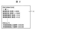
- FIG. 2 shows an example of the image information file 11.
- This information is constituted by the magnification information of each defect acquired by the defect inspection apparatus 1 and the review apparatus 2, the resolution of the image, information on the defect detection position in the image, and the like.
- the magnification of the defect image 10 is determined at the time of image acquisition. Therefore, the magnification at which the defect image 10 is acquired by using the magnification information of each defect included in the image information file 11. It is possible to adjust the magnification of the design layout 7 to the above.
- FIG. 3 is a diagram showing a defect classification procedure.
- the input 30 of the design layout 7 and the input 31 of the defect information 12 are performed, and preprocessing such as graphic conversion and format conversion is performed.
- the layer definition 32 of the design layout 7 to be superimposed on the defect image 10 is performed.
- the design layout 7 may be used for a plurality of layer numbers and a plurality of data types. Keep it.
- the design layout 7 may have a different coordinate system such that the center of the die is the origin and the defect information 12 is the origin at the lower left corner of the die.
- the design layout 7 and the defect information 12 may have the same pattern position at the same location. Register the origin with.
- sampling 34 based on the ADC classification category by the review device is performed as necessary. For example, it is also effective to filter random defects such as foreign matter and scratches and extract only categories that may be systematic defects such as short defects and open defects.
- the design layout 7 used for the matching 35 may be data for the entire chip, or data cut out in accordance with a fixed size or the size of the defect image 10 around the defect detection position, that is, a layout of a limited region. Good. For example, it may be data of a region that is 1.5 times or twice that of the defect image in view of the coordinate shift.
- a design layout 7 of an area in which the size of the defect image 10 is expanded by an amount that can cover the value in advance may be extracted by examining a value that may cause a coordinate shift. It is also possible to match by moving the design layout 7 on the defect image 10 as an area equal to or smaller than the defect image. Some combinations other than those exemplified here are conceivable. Note that the sampling 34 and matching 35 can be performed in reverse order.
- an arbitrary layer means an inspection target layer and other layers located in the upper layer and the lower layer, and a plurality of layers can be selected.
- the layer to be inspected is a PolySi layer
- a layer such as an N-type or P-type active region or field region below that layer, or a region (for example, a high breakdown voltage region) different from the breakdown voltage of a normal MOS Can be used to classify defects in detail or based on pattern information such as cells, peripheral circuits, and dummy patterns.
- the layout characteristics such as the pattern density near the defect, area ratio, minimum space dimension, and minimum line width are calculated 38.
- calculating the layout characteristics and grasping the statistical tendency are very effective for analyzing systematic defects.
- the statistical characteristics of each defect type are highlighted. For example, when the pattern density in the vicinity of the defect in the classified defect type tends to be high with respect to the pattern density distribution of the entire chip, it becomes clear that this defect type is likely to occur in the dense region of the pattern.
- the calculation of the layout characteristics of the entire chip is also very effective.
- the base layout is a normal MOS withstand voltage P type diffusion layer, a normal MOS withstand voltage N type diffusion layer, a high withstand voltage MOS P type diffusion layer, and a high withstand voltage MOS N type diffusion layer.
- the contact failure rate where the underlying layout is located in the P-type diffusion layer of the high breakdown voltage MOS is larger than the proportion of contacts located in the P type diffusion layer of the high breakdown voltage MOS in the entire chip, the P type of the high breakdown voltage MOS It becomes clear that the contact failure of the diffusion layer is large, that is, there is a systematic failure factor. Thus, it is very important to obtain the existence probability of each contact by analyzing the layout of the entire chip.
- sampling 34 matching 35
- superimposed display 36 automatic classification 37
- layout characteristic calculation 38 can be changed in order according to the purpose of use, and are not limited to those shown in FIG.
- FIG. 4 shows a user screen 40 in the defect classification device 4.
- Three screens are displayed simultaneously in the center of the screen.
- a defect image 10 acquired at the time of review is displayed on the right side, a design layout 7 at the same position where this defect is detected on the left side, and a superimposed image 42 with these two images displayed in the center.
- the matching status between the layout data and the review image can be confirmed at a glance.
- a plurality of collation layers can be displayed at the same time, and the influence between the layers can be confirmed while comparing the target layer and the image.
- the layout images can be moved manually, superimposed and readjusted.
- the defect image 7 is set as the basic position, and the design layout 10 is clicked on the movement button (up / down / left / right button) 43 and superimposed while shifting the position.
- the wafer map 44 displays a wafer map based on the defect coordinates detected by the defect inspection apparatus 1. Further, in the die map 45, it is possible to confirm in which part of the die a defect exists, and the location where the defect has occurred and circuit blocks such as a control circuit unit, an arithmetic circuit unit, and a RAM unit in the semiconductor device, The positional relationship of can also be confirmed.
- the defect displayed in the three-screen display at the center of the screen can be highlighted on the wafer map 44 or the die map 45. Further, when a defect to be viewed on the wafer map 44 or the die map 45 is clicked, the designated defect can be displayed on the three screens at the center of the screen.
- the graph display 46 the result of the ADC classification category and the result of classification by the defect classification device 4 can be graphed.
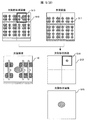
- FIG. 5A is a diagram illustrating a method of acquiring the defect shape image 52, and using this, a method of acquiring only the defect shape image 52 from the difference between the defect preprocessed image 50 and the reference image 51 that does not include a defect. Show about.
- the defect preprocessed image 50 may be the same as the defect image 10 described above, or may be a low-magnification image as compared with the defect image 10. However, when pattern matching between the defect preprocessed image 50 and the reference image 51 is performed, the magnifications of the defect preprocessed image 50 and the reference image 51 are set to be the same as possible, or one of the images is digitally zoomed to obtain a magnification. Keep them together. After matching is performed, the difference between the two images is taken, and a pixel in which a gradation difference exceeding a specified threshold value occurs is defined as a defective area, or a pixel group in which the pixel group exceeds a certain number of pixels. A defect shape image 52 is generated as a defect area. At this time, the defect shape image 52 may be a binarized image, or may be converted into an image having a small number of gradations.
- FIG. 5B is a diagram illustrating a second method illustrating a method for acquiring the defect shape image 52.
- the defect preprocessed image 510 is an image captured at a lower magnification than the defect image (defect review image) 10.
- the reference image 511 has the same magnification as the defect preprocessed image 510 to the extent that pattern matching can be performed. After matching is performed, the difference between the two images is taken, and a pixel in which a gradation difference exceeding a specified threshold value occurs is defined as a defective area, or a pixel group in which the pixel group exceeds a certain number of pixels.
- a defect shape image 512 is generated as a defect area.
- the defect image 10 is an image obtained by enlarging and imaging the portion indicated by the region 513 of the defect preprocessed image 510. Accordingly, a defect shape image 515 generated by enlarging the defect shape 10 in the region 514 corresponding to the region 513 to be equivalent to the defect image 10 by image processing is used as the defect shape image 52 to be superimposed on the design layout 7. be able to.
- FIG. 5C is a diagram showing a third method showing a method for acquiring the defect shape image 52.
- the defect preprocessed image 520 is an image captured at a lower magnification than the defect image (defect review image) 10.
- the defect shape image 521 can be obtained by utilizing the repeatability of the pattern.
- the defect image 10 is an image obtained by enlarging and imaging the portion indicated by the region 522 of the defect preprocessed image 520. Therefore, in the region 523 on the defect shape image 521 corresponding to the region 522, the defect shape image 524 enlarged by the image processing equivalent to the defect image 10 can be used as the defect shape image 52 superimposed on the design layout 7. .
- the defect image 520 is divided into local areas, and the image already stored for each area is stored.
- a defect shape image can be generated by a method of performing matching with a local region, obtaining a difference between the matched local regions, and extracting a defect region.
- defect shape image 521 from the defect image 520 by using an algorithm for automatically detecting an abnormal part from an arbitrary image.
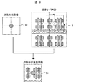
- FIG. 6 is a diagram showing a procedure for superimposing the defect shape image 52 on the design layout 7.
- the defect shape image 52 is superimposed on the design layout 7 based on the above-described matching positional relationship between the defect image 10 and the design layout 7 and the positional relationship between the defect image 10 and the defect preprocessed image 50.
- the magnifications of the design layout 7 and the defect shape image 52 are matched. Thereby, the defect shape superimposed image 53 can be generated.
- the defect shape can be assumed to be circular, and the defect shape can be virtually drawn and superimposed on the design layout 7.
- This defect size can be acquired from the defect inspection apparatus 1 or the review apparatus 2 described above.
- the contact or via part may appear as an abnormal contrast.
- the defect coordinates and the hole diameter are known, an image can be generated and superimposed based on the defect coordinates and the hole diameter.
- the defect size may be obtained from any one of the defect inspection apparatus 1, the review apparatus 2, and the design layout 7 described above.
- the defect shape image 52 can be generated from the pattern recognition of the defect image 10.
- the number of layers of the pattern is set in advance, and based on this, the pattern existing in the defect image 10 is identified for each layer, and the pattern expansion, contraction, or isolation from the irregularity or discontinuity of the image This is a general technique for extracting a sigma and considering this as a defect. It is also effective to generate the defect shape image 52 from this extraction.
- the reviewed defect occurrence area is a repeated pattern area.
- a method is used in which the repeatability of the pattern is analyzed from normal image regions other than the region affected by the defect, the normal image of the region affected by the defect is estimated, and the reference image 51 is virtually generated. It is also effective.
- the defect image 10 is divided into local regions, and local images of the image already stored for each region are stored.
- a defect is detected from the defect image 10 by applying a method of extracting a defect area by performing a matching with an area and obtaining a difference between the matched local areas or an algorithm for automatically detecting an abnormal part from an arbitrary image. It is also possible to generate the shape image 52.
- FIG. 7 is a diagram showing a method for defining and classifying the overlapping state of the layout pattern 60 and the defect 61, which is generated by superimposing the design layout 7 and the defect shape image 52.
- FIG. 7 the inside of the pattern, the pattern crossing, and the outside of the pattern are determined according to the three states.
- the pattern straddling in FIG. 7B means a category in which the defect 61 exists so as to protrude from the layout pattern 60.
- the above determination can be realized, for example, by converting the layout pattern 60 into pixel information and collating each defective pixel 62 of the defect 61 with each pixel of the layout pattern 60.
- the defect outline 63 corresponding to the outermost periphery of the defect 61 is extracted, and the defect outline 63 and the layout pattern 40 are collated.
- the defect classified in the pattern as shown in FIG. 7A is classified in more detail depending on whether it touches the edge boundary of the pattern, the pixel of the edge boundary of the layout pattern 60 is identified.
- the defect classified outside the pattern as shown in FIG. 7C is classified in more detail depending on whether it touches the edge boundary of the pattern, the pixel at the edge boundary of the layout pattern 60 is identified.
- the overlap state is determined by the design layout 7 of the same layer as the process in which the defect 61 is reviewed.
- the overlap state with the layout pattern of other layers can be classified as a reference. is there. It is also effective to extract systematic defects by combining the classification results in a plurality of layers.
- a category of defect classification it is also effective to distinguish an overlapping state with a plurality of layout patterns such as a bridge defect from an overlapping state with one layout pattern.
- the above classification is based on the premise that the defect shape image 52 can be accurately generated from the defect image 10 and the defect shape image 52 can be accurately superimposed on the design layout 7.
- the defect 61 may be generated larger or smaller than the actual defect, or there may be a positional shift when the defect shape image 52 and the design layout 7 are superimposed. The following describes how to deal with these problems.
- FIG. 8 is a diagram showing a method for improving the classification accuracy.
- FIG. 8A shows the layout pattern 60 and a defect 61 ′ having a shape error, and the actual shape of the defect 61 is indicated by a dotted line.
- the defect 61 ′ having a shape error protrudes from the layout pattern 60, the defect 61 ′ is erroneously classified across the patterns, but in reality, it should be classified within the pattern.
- FIG. 8B shows a method of widening the layout pattern 60 to absorb this shape error.
- the layout pattern 60 is widened by ⁇ . According to this method, it is possible to classify the defect 61 'having a shape error into the pattern.
- This layout pattern widening method can also be applied to discriminating systematic defects that occur at a location away from the layout pattern by a certain distance. In this case, similarly, the systematic defect can be detected by expanding the layout pattern by a certain distance and counting the classification results that are straddled or inside.
- FIG. 8C shows a method of improving the classification accuracy by calculating the area ratio of the defect 61 ′ having a shape error.
- An area where a defect 61 ′ having a shape error overlaps with the layout pattern 60 is A, and an area where the defect 61 ′ protrudes is B.
- the ratio of the overlapped area A to the total defect area (A + B) is equal to or greater than the specified threshold value, it is possible to improve the classification accuracy by determining that it is within the pattern.
- defect outline 63 (described in FIG. 7)
- the length of the outline extending from the layout pattern 60 is equal to or less than a specified threshold value
- defects can be efficiently and effectively classified by determining with high accuracy the overlapping state (inside pattern / between patterns / outside pattern) between the design layout pattern and the defect. Furthermore, it becomes possible to identify a systematic defect that has become a problem in recent fine devices. Eventually, the classification of systematic defects makes it possible to quickly increase the yield in semiconductor device development, prototyping, and mass production.
Landscapes
- Physics & Mathematics (AREA)
- Health & Medical Sciences (AREA)
- Life Sciences & Earth Sciences (AREA)
- Chemical & Material Sciences (AREA)
- Analytical Chemistry (AREA)
- Biochemistry (AREA)
- General Health & Medical Sciences (AREA)
- General Physics & Mathematics (AREA)
- Immunology (AREA)
- Pathology (AREA)
- Engineering & Computer Science (AREA)
- Computer Vision & Pattern Recognition (AREA)
- Signal Processing (AREA)
- Testing Or Measuring Of Semiconductors Or The Like (AREA)
- Investigating Materials By The Use Of Optical Means Adapted For Particular Applications (AREA)
Abstract
Description
2 レビュー装置
3 欠陥情報サーバ
4 欠陥分類装置
5 設計データベース
6 通信ネットワーク
7 設計レイアウト
8 クリーンルーム
9 欠陥データ
10 欠陥画像
11 画像情報ファイル
12 欠陥情報
20 ネットワークインターフェィス
21 主記憶装置
22 レイアウト変換演算部
23 サンプリング部
24 マッチング処理部
25 欠陥形状画像抽出部
26 重畳処理部
27 欠陥分類部
28 レイアウト特性演算部
29 ユーザインターフェース
Claims (30)
- 半導体デバイスの欠陥を検出する欠陥検査装置と観察を行うレビュー装置によって前記欠陥を分類する欠陥分類装置の欠陥分類方法であって、
前記欠陥分類装置において、
前記欠陥の検査レイヤにおける前記欠陥検査装置または前記レビュー装置の欠陥画像と、
前記半導体デバイスの設計レイアウトデータとのパターンマッチングを行い、
前記検査レイヤ、前記検査レイヤの上層、または、前記検査レイヤの下層の少なくともいずれか一層の設計レイアウトパターンに前記欠陥を重畳し、
前記欠陥と前記任意のレイヤのレイアウトパターンの重なり状態を判定して、自動分類することを特徴とする半導体欠陥分類方法。 - 請求項1に記載の半導体欠陥分類方法であって、
前記欠陥画像と、前記欠陥を含まない参照画像との差分から欠陥形状画像を生成し、
前記設計レイアウトパターンに前記欠陥形状画像を重畳し、
前記欠陥と前記任意のレイヤのレイアウトパターンの重なり状態を判定して、自動分類することを特徴とする半導体欠陥分類方法。 - 請求項1に記載の半導体欠陥分類方法であって、
前記欠陥画像のパターン認識により欠陥形状画像を生成し、
前記設計レイアウトパターンに前記欠陥形状画像を重畳し、
前記欠陥と前記任意のレイヤのレイアウトパターンの重なり状態を判定して、自動分類することを特徴とする半導体欠陥分類方法。 - 請求項1に記載の半導体欠陥分類方法であって、
前記欠陥検査装置または前記レビュー装置から欠陥座標を取得し、
前記欠陥検査装置、前記レビュー装置、前記設計レイアウトパターンのいずれか一つから欠陥サイズを取得し、
前記設計レイアウトパターンにおける前記欠陥座標の位置関係と前記欠陥サイズに基づいて、前記欠陥と前記任意のレイヤのレイアウトパターンの重なり状態を判定して、自動分類することを特徴とする半導体欠陥分類方法。 - 請求項1および3に記載の半導体欠陥分類方法であって、
前記欠陥形状画像から輪郭線を抽出し、
前記設計レイアウトパターンに前記輪郭線を重畳し、
前記欠陥と前記任意のレイヤのレイアウトパターンの重なり状態を判定して、自動分類することを特徴とする半導体欠陥分類方法。 - 請求項1から5に記載の半導体欠陥分類方法であって、
前記欠陥の重なり状態を、パターン内にあるか、パターンに跨っているか、または、パターンの外にあるかによって、前記欠陥と前記任意のレイヤのレイアウトパターンの重なり状態を判定して、自動分類することを特徴とする半導体欠陥分類方法。 - 請求項1から4に記載の半導体欠陥分類方法であって、
前記欠陥の重なり状態を、前記欠陥形状画像の総面積と前記欠陥形状画像のパターン内の面積との比率に基づいて、パターン内にあるか、パターンに跨っているか、または、パターンの外にあるかによって、前記欠陥と前記任意のレイヤのレイアウトパターンの重なり状態を判定して、自動分類することを特徴とする半導体欠陥分類方法。 - 請求項5に記載の半導体欠陥分類方法であって、
前記欠陥の重なり状態を、前記輪郭線の長さとパターンからはみ出した長さとの比率に基づいて、パターン内にあるか、パターンに跨っているか、または、パターンの外にあるかによって、前記欠陥と前記任意のレイヤのレイアウトパターンの重なり状態を判定して、自動分類することを特徴とする半導体欠陥分類方法。 - 請求項1から8に記載の半導体欠陥分類方法であって、
前記設計レイアウトパターンを拡幅、もしくは、縮退させて、
前記欠陥と前記任意のレイヤのレイアウトパターンの重なり状態を判定して、自動分類することを特徴とする半導体欠陥分類方法。 - 請求項1から9に記載の半導体欠陥分類方法であって、
前記欠陥の分類欠陥結果、あるいは、前記欠陥の近傍におけるパターン密度,面積率,最小スペース寸法,最小線幅のいずれか一つについて、チップ全体の傾向と比較することにより、統計的にシステマティック欠陥を抽出することを特徴とする半導体欠陥分類方法。 - 半導体デバイスの欠陥を検出する欠陥検査装置と観察を行うレビュー装置によって前記欠陥を分類する欠陥分類装置であって、
前記欠陥分類装置が、
設計レイアウトの入力を受ける手段と、
前記欠陥検査装置もしくはレビュー装置から出力される欠陥情報の入力を受ける手段と、
前記欠陥情報に含まれる欠陥画像と重畳する前記設計レイアウトパターンのレイヤ指定を受ける手段と、
前記欠陥情報と前記設計レイアウトパターンの原点合わせ設定を受ける手段と、
前記欠陥画像と前記設計レイアウトパターンのパターンマッチングを行う手段と、
前記欠陥と前記任意のレイヤのレイアウトパターンの重なり状態に基づいて自動分類を行う手段と、を有することを特徴とする半導体欠陥分類装置。 - 請求項11に記載の半導体欠陥分類装置であって、
前記欠陥分類装置が、
前記欠陥画像と、欠陥を含まない参照画像との差分から欠陥形状画像を生成する手段と、
前記設計レイアウトパターンに前記欠陥形状画像を重畳して、前記欠陥と前記任意のレイヤのレイアウトパターンの重なり状態を判定して、自動分類する手段と、
を有することを特徴とする半導体欠陥分類装置。 - 請求項11に記載の半導体欠陥分類装置であって、
前記欠陥分類装置が、
前記欠陥画像のパターン認識から欠陥形状画像を生成する手段と、
前記設計レイアウトパターンに前記欠陥形状画像を重畳して、前記欠陥と前記任意のレイヤのレイアウトパターンの重なり状態を判定して、自動分類する手段と、を有することを特徴とする半導体欠陥分類装置。 - 請求項11に記載の半導体欠陥分類装置であって、
前記欠陥分類装置が、
前記欠陥検査装置または前記レビュー装置から欠陥座標を取得する手段と、
前記欠陥検査装置、前記レビュー装置、前記設計レイアウトパターンのいずれか一つから欠陥サイズを取得する手段と、
前記設計レイアウトパターンにおける前記欠陥座標の位置関係と前記欠陥サイズに基づいて、前記欠陥と前記任意のレイヤのレイアウトパターンの重なり状態を判定して、自動分類する手段と、を有することを特徴とする半導体欠陥分類装置。 - 請求項11および13に記載の半導体欠陥分類装置であって、
前記欠陥分類装置が、
前記欠陥形状画像から輪郭線を抽出する手段と、
前記設計レイアウトパターンに前記輪郭線を重畳して、前記欠陥と前記任意のレイヤのレイアウトパターンの重なり状態を判定して、自動分類する手段と、を有することを特徴とする半導体欠陥分類装置。 - 請求項11から15に記載の半導体欠陥分類装置であって、
前記欠陥分類装置が、
前記欠陥の重なり状態を、パターン内にあるか、パターンに跨っているか、または、パターンの外にあるかによって、前記欠陥と前記任意のレイヤのレイアウトパターンの重なり状態を判定して、自動分類する手段と、を実行させる手段を有することを特徴とする半導体欠陥分類装置。 - 請求項11から14に記載の半導体欠陥分類装置であって、
前記欠陥分類装置が、
前記欠陥の重なり状態を、前記欠陥形状画像の総面積と前記欠陥形状画像のパターン内の面積との比率に基づいて、パターン内にあるか、パターンに跨っているか、または、パターンの外にあるかによって、前記欠陥と前記任意のレイヤのレイアウトパターンの重なり状態を判定して、自動分類する手段と、を有することを特徴とする半導体欠陥分類装置。 - 請求項15に記載の半導体欠陥分類装置であって、
前記欠陥分類装置が、
前記欠陥の重なり状態を、前記輪郭線の長さとパターンからはみ出した長さとの比率に基づいて、パターン内にあるか、パターンに跨っているか、または、パターンの外にあるかによって、前記欠陥と前記任意のレイヤのレイアウトパターンの重なり状態を判定して、自動分類する手段と、を有することを特徴とする半導体欠陥分類装置。 - 請求項11から18に記載の半導体欠陥分類装置であって、
前記欠陥分類装置が、
前記設計レイアウトパターンを拡幅、もしくは、縮退させて、
前記欠陥と前記任意のレイヤのレイアウトパターンの重なり状態を判定して、欠陥分類する手段と、を有することを特徴とする半導体欠陥分類装置。 - 請求項11から19に記載の半導体欠陥分類装置であって、
前記欠陥分類装置が、
前記欠陥の分類欠陥結果、あるいは、前記欠陥の近傍におけるパターン密度,面積率,最小スペース寸法,最小線幅のいずれか一つについて、チップ全体の傾向と比較する手段と、を有することを特徴とする半導体欠陥分類装置。 - 半導体デバイスの欠陥を検出する欠陥検査装置と観察を行うレビュー装置によって前記欠陥を分類する欠陥分類プログラムであって、
前記欠陥分類プログラムが、
設計レイアウトの入力を受けるステップと、
前記欠陥検査装置もしくはレビュー装置から出力される欠陥情報の入力を受けるステップと、
前記欠陥情報に含まれる欠陥画像と重畳する前記設計レイアウトパターンのレイヤ指定を受けるステップと、
前記欠陥情報と前記設計レイアウトパターンの原点合わせ設定を受けるステップと、
前記欠陥画像と前記設計レイアウトパターンのパターンマッチングを行うステップと、
前記欠陥と前記任意のレイヤのレイアウトパターンの重なり状態に基づいて自動分類を行うステップと、を実行させることを特徴とする半導体欠陥分類プログラム。 - 請求項21に記載の半導体欠陥分類プログラムであって、
前記欠陥分類プログラムが、
前記欠陥画像と、欠陥を含まない参照画像との差分から欠陥形状画像を生成するステップと、
前記設計レイアウトパターンに前記欠陥形状画像を重畳して、前記欠陥と前記任意のレイヤのレイアウトパターンの重なり状態を判定して、自動分類するステップと、を実行させることを特徴とする半導体欠陥分類プログラム。 - 請求項21に記載の半導体欠陥分類プログラムであって、
前記欠陥分類プログラムが、
前記欠陥画像のパターン認識から欠陥形状画像を生成するステップと、
前記設計レイアウトパターンに前記欠陥形状画像を重畳して、前記欠陥と前記任意のレイヤのレイアウトパターンの重なり状態を判定して、自動分類するステップと、を実行させることを特徴とする半導体欠陥分類プログラム。 - 請求項21に記載の半導体欠陥分類プログラムであって、
前記欠陥分類プログラムが、
前記欠陥検査装置または前記レビュー装置から欠陥座標を取得するステップと、
前記欠陥検査装置、前記レビュー装置、前記設計レイアウトパターンのいずれか一つから欠陥サイズを取得するステップと、
前記設計レイアウトパターンにおける前記欠陥座標の位置関係と前記欠陥サイズに基づいて、前記欠陥と前記任意のレイヤのレイアウトパターンの重なり状態を判定して、自動分類するステップと、を実行させることを特徴とする半導体欠陥分類プログラム。 - 請求項21および23に記載の半導体欠陥分類プログラムであって、
前記欠陥分類プログラムが、
前記欠陥形状画像から輪郭線を抽出するステップと、
前記設計レイアウトパターンに前記輪郭線を重畳して、前記欠陥と前記任意のレイヤのレイアウトパターンの重なり状態を判定して、自動分類するステップと、
を実行させることを特徴とする半導体欠陥分類プログラム。 - 請求項21から25に記載の半導体欠陥分類プログラムであって、
前記欠陥分類プログラムが、
前記欠陥の重なり状態を、パターン内にあるか、パターンに跨っているか、または、パターンの外にあるかによって、前記欠陥と前記任意のレイヤのレイアウトパターンの重なり状態を判定して、自動分類するステップと、を実行させるステップを実行させることを特徴とする半導体欠陥分類プログラム。 - 請求項21から24に記載の半導体欠陥分類プログラムであって、
前記欠陥分類プログラムが、
前記欠陥の重なり状態を、前記欠陥形状画像の総面積と前記欠陥形状画像のパターン内の面積との比率に基づいて、パターン内にあるか、パターンに跨っているか、または、パターンの外にあるかによって、前記欠陥と前記任意のレイヤのレイアウトパターンの重なり状態を判定して、自動分類するステップと、を実行させることを特徴とする半導体欠陥分類プログラム。 - 請求項25に記載の半導体欠陥分類プログラムであって、
前記欠陥分類プログラムが、
前記欠陥の重なり状態を、前記輪郭線の長さとパターンからはみ出した長さとの比率に基づいて、パターン内にあるか、パターンに跨っているか、または、パターンの外にあるかによって、前記欠陥と前記任意のレイヤのレイアウトパターンの重なり状態を判定して、自動分類するステップと、を実行させることを特徴とする半導体欠陥分類プログラム。 - 請求項21から28に記載の半導体欠陥分類プログラムであって、
前記欠陥分類プログラムが、
前記設計レイアウトパターンを拡幅、もしくは、縮退させることにより、前記欠陥と前記任意のレイヤのレイアウトパターンの重なり状態を判定して、欠陥分類するステップと、
を実行させることを特徴とする半導体欠陥分類プログラム。 - 請求項21から29に記載の半導体欠陥分類プログラムであって、
前記欠陥分類プログラムが、
前記欠陥の分類欠陥結果、あるいは、前記欠陥の近傍におけるパターン密度,面積率,最小スペース寸法,最小線幅のいずれか一つについて、チップ全体の傾向と比較するステップと、を実行させることを特徴とする半導体欠陥分類プログラム。
Priority Applications (2)
| Application Number | Priority Date | Filing Date | Title |
|---|---|---|---|
| JP2011521783A JPWO2011004534A1 (ja) | 2009-07-09 | 2010-05-14 | 半導体欠陥分類方法,半導体欠陥分類装置,半導体欠陥分類プログラム |
| US13/382,437 US8595666B2 (en) | 2009-07-09 | 2010-05-14 | Semiconductor defect classifying method, semiconductor defect classifying apparatus, and semiconductor defect classifying program |
Applications Claiming Priority (2)
| Application Number | Priority Date | Filing Date | Title |
|---|---|---|---|
| JP2009-162334 | 2009-07-09 | ||
| JP2009162334 | 2009-07-09 |
Publications (1)
| Publication Number | Publication Date |
|---|---|
| WO2011004534A1 true WO2011004534A1 (ja) | 2011-01-13 |
Family
ID=43428967
Family Applications (1)
| Application Number | Title | Priority Date | Filing Date |
|---|---|---|---|
| PCT/JP2010/003259 Ceased WO2011004534A1 (ja) | 2009-07-09 | 2010-05-14 | 半導体欠陥分類方法,半導体欠陥分類装置,半導体欠陥分類プログラム |
Country Status (3)
| Country | Link |
|---|---|
| US (1) | US8595666B2 (ja) |
| JP (1) | JPWO2011004534A1 (ja) |
| WO (1) | WO2011004534A1 (ja) |
Cited By (11)
| Publication number | Priority date | Publication date | Assignee | Title |
|---|---|---|---|---|
| KR20130118278A (ko) * | 2012-04-19 | 2013-10-29 | 어플라이드 머티리얼즈 이스라엘 리미티드 | Cad-기반 컨텍스트 속성들을 사용하는 결함 분류 |
| JP2013225618A (ja) * | 2012-04-23 | 2013-10-31 | Hitachi High-Technologies Corp | 半導体欠陥分類装置及び半導体欠陥分類装置用のプログラム |
| WO2013168487A1 (ja) * | 2012-05-11 | 2013-11-14 | 株式会社 日立ハイテクノロジーズ | 欠陥解析支援装置、欠陥解析支援装置で実行されるプログラム、および欠陥解析システム |
| JP2016502750A (ja) * | 2012-10-15 | 2016-01-28 | ケーエルエー−テンカー コーポレイション | 欠陥特定情報を用いるウェハ上の欠陥の検出 |
| KR20160029421A (ko) * | 2014-09-05 | 2016-03-15 | 삼성전자주식회사 | 반도체 소자의 패턴 분석방법 |
| JP2018525811A (ja) * | 2015-08-12 | 2018-09-06 | ケーエルエー−テンカー コーポレイション | 設計を利用する先行層欠陥箇所の点検 |
| JP2019509628A (ja) * | 2016-02-04 | 2019-04-04 | ケーエルエー−テンカー コーポレイション | デザインファイルまたは検査画像を用いた自動デスキュー |
| WO2019186915A1 (ja) * | 2018-03-29 | 2019-10-03 | 三菱電機株式会社 | 異常検査装置および異常検査方法 |
| US11726403B2 (en) | 2019-10-11 | 2023-08-15 | Canon Kabushiki Kaisha | Information processing apparatus, information processing method, and computer program |
| WO2024069737A1 (ja) * | 2022-09-27 | 2024-04-04 | 株式会社日立ハイテク | 検査方法および荷電粒子線装置 |
| US12079310B2 (en) | 2021-03-11 | 2024-09-03 | Kabushiki Kaisha Toshiba | Defect classification apparatus, method and program |
Families Citing this family (25)
| Publication number | Priority date | Publication date | Assignee | Title |
|---|---|---|---|---|
| KR101205970B1 (ko) * | 2010-11-18 | 2012-11-28 | 주식회사 고영테크놀러지 | 브리지 연결불량 검출방법 |
| US9595091B2 (en) | 2012-04-19 | 2017-03-14 | Applied Materials Israel, Ltd. | Defect classification using topographical attributes |
| JP6255706B2 (ja) * | 2013-04-22 | 2018-01-10 | 富士通株式会社 | 表示制御装置、表示制御方法、表示制御プログラムおよび情報提供システム |
| JP6244954B2 (ja) | 2014-02-06 | 2017-12-13 | 富士通株式会社 | 端末装置、情報処理装置、表示制御方法、及び表示制御プログラム |
| KR102392057B1 (ko) | 2014-12-22 | 2022-04-28 | 삼성전자주식회사 | 자동 결함 분류 방법 |
| CN104503202B (zh) * | 2014-12-25 | 2018-10-16 | 上海华虹宏力半导体制造有限公司 | 重复设计单元的区分方法 |
| US9940704B2 (en) * | 2015-06-19 | 2018-04-10 | KLA—Tencor Corporation | Pre-layer defect site review using design |
| KR20170083678A (ko) * | 2016-01-08 | 2017-07-19 | 삼성전자주식회사 | 기판 검사 방법 |
| US10204416B2 (en) * | 2016-02-04 | 2019-02-12 | Kla-Tencor Corporation | Automatic deskew using design files or inspection images |
| JP6333871B2 (ja) * | 2016-02-25 | 2018-05-30 | ファナック株式会社 | 入力画像から検出した対象物を表示する画像処理装置 |
| US10192302B2 (en) * | 2016-05-25 | 2019-01-29 | Kla-Tencor Corporation | Combined patch and design-based defect detection |
| EP3486638B1 (en) * | 2016-07-12 | 2023-09-20 | Yoshino Gypsum Co., Ltd. | Inspection method, inspection and reporting method, manufacturing method including the inspection method, inspection apparatus, and manufacturing apparatus |
| US20180329801A1 (en) * | 2017-05-15 | 2018-11-15 | Microsoft Technology Licensing, Llc | Detecting and correcting layout anomalies in real-time |
| US10402963B2 (en) * | 2017-08-24 | 2019-09-03 | Kla-Tencor Corporation | Defect detection on transparent or translucent wafers |
| JP7053417B2 (ja) | 2018-09-13 | 2022-04-12 | キオクシア株式会社 | 欠陥検査装置および欠陥検査方法 |
| US11475556B2 (en) | 2019-05-30 | 2022-10-18 | Bruker Nano, Inc. | Method and apparatus for rapidly classifying defects in subcomponents of manufactured component |
| CN111353983B (zh) * | 2020-02-28 | 2023-05-23 | 腾讯科技(深圳)有限公司 | 缺陷检测识别方法、装置、计算机可读介质及电子设备 |
| TW202518007A (zh) * | 2020-04-10 | 2025-05-01 | 荷蘭商Asml荷蘭公司 | 促進晶圓之檢測的方法與設備及相關聯非暫時性電腦可讀媒體 |
| US11861286B2 (en) * | 2020-06-30 | 2024-01-02 | Synopsys, Inc. | Segregating defects based on computer-aided design (CAD) identifiers associated with the defects |
| TWI768434B (zh) * | 2020-08-19 | 2022-06-21 | 萬潤科技股份有限公司 | 電路板資訊顯示方法及裝置 |
| CN113743447B (zh) * | 2021-07-15 | 2024-05-17 | 上海朋熙半导体有限公司 | 半导体瑕疵识别方法、装置、计算机设备和存储介质 |
| KR20240011046A (ko) | 2022-07-18 | 2024-01-25 | 삼성전자주식회사 | 기판 검사 방법 |
| KR20240111103A (ko) | 2023-01-09 | 2024-07-16 | 삼성전자주식회사 | 반도체 장치의 검사 방법 |
| CN119271834A (zh) * | 2024-09-25 | 2025-01-07 | 江苏维普光电科技有限公司 | 用于半导体掩膜检测缺陷的可视化展示方法 |
| CN119558422B (zh) * | 2025-01-23 | 2025-05-13 | 山东云海国创云计算装备产业创新中心有限公司 | 器件检测方法、装置、计算机设备、存储介质及程序产品 |
Citations (3)
| Publication number | Priority date | Publication date | Assignee | Title |
|---|---|---|---|---|
| JP2003086645A (ja) * | 2001-09-13 | 2003-03-20 | Hitachi Ltd | 検査装置および検査システム並びに半導体デバイスの製造方法 |
| JP2009010286A (ja) * | 2007-06-29 | 2009-01-15 | Hitachi High-Technologies Corp | 半導体欠陥分類方法、半導体欠陥分類装置、半導体欠陥分類装置のプログラム、半導体欠陥検査方法、および、半導体欠陥検査システム |
| JP2009516832A (ja) * | 2005-11-18 | 2009-04-23 | ケーエルエー−テンカー テクノロジィース コーポレイション | 検査データと組み合わせて設計データを使用するための方法及びシステム |
Family Cites Families (7)
| Publication number | Priority date | Publication date | Assignee | Title |
|---|---|---|---|---|
| JPH01259245A (ja) | 1988-04-08 | 1989-10-16 | Hitachi Ltd | パターン検査方法 |
| JP2653853B2 (ja) | 1988-10-11 | 1997-09-17 | 大日本印刷株式会社 | 周期性パターンの検査方法 |
| JP2942171B2 (ja) | 1995-06-09 | 1999-08-30 | 大日本スクリーン製造株式会社 | プリント基板のパターン検査装置 |
| US6977183B1 (en) * | 2002-07-18 | 2005-12-20 | Kla-Tencor Technologies Corporation | Process for locating, displaying, analyzing, and optionally monitoring potential transient defect sites in one or more integrated circuit chips of a semiconductor substrate |
| US7608468B1 (en) * | 2003-07-02 | 2009-10-27 | Kla-Tencor Technologies, Corp. | Apparatus and methods for determining overlay and uses of same |
| US9002497B2 (en) * | 2003-07-03 | 2015-04-07 | Kla-Tencor Technologies Corp. | Methods and systems for inspection of wafers and reticles using designer intent data |
| DE102005055753B4 (de) | 2005-11-21 | 2007-10-11 | Wipotec Wiege- Und Positioniersysteme Gmbh | Wägezelle für bewegte Güter |
-
2010
- 2010-05-14 JP JP2011521783A patent/JPWO2011004534A1/ja active Pending
- 2010-05-14 WO PCT/JP2010/003259 patent/WO2011004534A1/ja not_active Ceased
- 2010-05-14 US US13/382,437 patent/US8595666B2/en active Active
Patent Citations (3)
| Publication number | Priority date | Publication date | Assignee | Title |
|---|---|---|---|---|
| JP2003086645A (ja) * | 2001-09-13 | 2003-03-20 | Hitachi Ltd | 検査装置および検査システム並びに半導体デバイスの製造方法 |
| JP2009516832A (ja) * | 2005-11-18 | 2009-04-23 | ケーエルエー−テンカー テクノロジィース コーポレイション | 検査データと組み合わせて設計データを使用するための方法及びシステム |
| JP2009010286A (ja) * | 2007-06-29 | 2009-01-15 | Hitachi High-Technologies Corp | 半導体欠陥分類方法、半導体欠陥分類装置、半導体欠陥分類装置のプログラム、半導体欠陥検査方法、および、半導体欠陥検査システム |
Cited By (27)
| Publication number | Priority date | Publication date | Assignee | Title |
|---|---|---|---|---|
| KR102132328B1 (ko) * | 2012-04-19 | 2020-07-10 | 어플라이드 머티리얼즈 이스라엘 리미티드 | Cad-기반 컨텍스트 속성들을 사용하는 결함 분류 |
| JP2013225312A (ja) * | 2012-04-19 | 2013-10-31 | Applied Materials Israel Ltd | Cadベースのコンテクスト属性を利用した欠陥分類 |
| US9858658B2 (en) | 2012-04-19 | 2018-01-02 | Applied Materials Israel Ltd | Defect classification using CAD-based context attributes |
| KR20130118278A (ko) * | 2012-04-19 | 2013-10-29 | 어플라이드 머티리얼즈 이스라엘 리미티드 | Cad-기반 컨텍스트 속성들을 사용하는 결함 분류 |
| JP2013225618A (ja) * | 2012-04-23 | 2013-10-31 | Hitachi High-Technologies Corp | 半導体欠陥分類装置及び半導体欠陥分類装置用のプログラム |
| WO2013161577A1 (ja) * | 2012-04-23 | 2013-10-31 | 株式会社日立ハイテクノロジーズ | 半導体欠陥分類装置及び半導体欠陥分類装置用のプログラム |
| US20150213596A1 (en) * | 2012-04-23 | 2015-07-30 | Hitachi High-Technologies Corporation | Semiconductor defect categorization device and program for semiconductor defect categorization device |
| KR101760559B1 (ko) * | 2012-04-23 | 2017-07-21 | 가부시키가이샤 히다치 하이테크놀로지즈 | 반도체 결함 분류 장치 및 반도체 결함 분류 장치용 프로그램을 기록한 비일시적인 컴퓨터 판독 가능 기록 매체 |
| US9881365B2 (en) | 2012-04-23 | 2018-01-30 | Hitachi High-Technologies Corporation | Semiconductor defect categorization device and program for semiconductor defect categorization device |
| JP2013236032A (ja) * | 2012-05-11 | 2013-11-21 | Hitachi High-Technologies Corp | 欠陥解析支援装置、欠陥解析支援装置で実行されるプログラム、および欠陥解析システム |
| US9582875B2 (en) | 2012-05-11 | 2017-02-28 | Hitachi High-Technologies Corporation | Defect analysis assistance device, program executed by defect analysis assistance device, and defect analysis system |
| TWI512787B (zh) * | 2012-05-11 | 2015-12-11 | 日立全球先端科技股份有限公司 | A defect analysis support means, a program executed by the defect analysis support means, and a defect analysis system |
| WO2013168487A1 (ja) * | 2012-05-11 | 2013-11-14 | 株式会社 日立ハイテクノロジーズ | 欠陥解析支援装置、欠陥解析支援装置で実行されるプログラム、および欠陥解析システム |
| JP2016502750A (ja) * | 2012-10-15 | 2016-01-28 | ケーエルエー−テンカー コーポレイション | 欠陥特定情報を用いるウェハ上の欠陥の検出 |
| KR20160029421A (ko) * | 2014-09-05 | 2016-03-15 | 삼성전자주식회사 | 반도체 소자의 패턴 분석방법 |
| KR102310123B1 (ko) * | 2014-09-05 | 2021-10-08 | 삼성전자주식회사 | 반도체 소자의 패턴 분석방법 |
| JP2018525811A (ja) * | 2015-08-12 | 2018-09-06 | ケーエルエー−テンカー コーポレイション | 設計を利用する先行層欠陥箇所の点検 |
| JP2019509628A (ja) * | 2016-02-04 | 2019-04-04 | ケーエルエー−テンカー コーポレイション | デザインファイルまたは検査画像を用いた自動デスキュー |
| KR20200116532A (ko) * | 2018-03-29 | 2020-10-12 | 미쓰비시덴키 가부시키가이샤 | 이상 검사 장치 및 이상 검사 방법 |
| JPWO2019186915A1 (ja) * | 2018-03-29 | 2020-05-28 | 三菱電機株式会社 | 異常検査装置および異常検査方法 |
| KR102206698B1 (ko) | 2018-03-29 | 2021-01-22 | 미쓰비시덴키 가부시키가이샤 | 이상 검사 장치 및 이상 검사 방법 |
| TWI719357B (zh) * | 2018-03-29 | 2021-02-21 | 日商三菱電機股份有限公司 | 異常檢查裝置以及異常檢查方法 |
| WO2019186915A1 (ja) * | 2018-03-29 | 2019-10-03 | 三菱電機株式会社 | 異常検査装置および異常検査方法 |
| US11726403B2 (en) | 2019-10-11 | 2023-08-15 | Canon Kabushiki Kaisha | Information processing apparatus, information processing method, and computer program |
| US12079310B2 (en) | 2021-03-11 | 2024-09-03 | Kabushiki Kaisha Toshiba | Defect classification apparatus, method and program |
| WO2024069737A1 (ja) * | 2022-09-27 | 2024-04-04 | 株式会社日立ハイテク | 検査方法および荷電粒子線装置 |
| JPWO2024069737A1 (ja) * | 2022-09-27 | 2024-04-04 |
Also Published As
| Publication number | Publication date |
|---|---|
| US20120131529A1 (en) | 2012-05-24 |
| US8595666B2 (en) | 2013-11-26 |
| JPWO2011004534A1 (ja) | 2012-12-13 |
Similar Documents
| Publication | Publication Date | Title |
|---|---|---|
| WO2011004534A1 (ja) | 半導体欠陥分類方法,半導体欠陥分類装置,半導体欠陥分類プログラム | |
| US7760929B2 (en) | Grouping systematic defects with feedback from electrical inspection | |
| US7760347B2 (en) | Design-based method for grouping systematic defects in lithography pattern writing system | |
| JP4791267B2 (ja) | 欠陥検査システム | |
| JP6078234B2 (ja) | 荷電粒子線装置 | |
| JP5081590B2 (ja) | 欠陥観察分類方法及びその装置 | |
| JP5479782B2 (ja) | 欠陥画像処理装置、欠陥画像処理方法、半導体欠陥分類装置および半導体欠陥分類方法 | |
| JP6080379B2 (ja) | 半導体欠陥分類装置及び半導体欠陥分類装置用のプログラム | |
| JP5460662B2 (ja) | 領域決定装置、観察装置または検査装置、領域決定方法および領域決定方法を用いた観察方法または検査方法 | |
| JP5357725B2 (ja) | 欠陥検査方法及び欠陥検査装置 | |
| JP5568456B2 (ja) | 荷電粒子線装置 | |
| JP5068591B2 (ja) | 半導体欠陥分類方法、半導体欠陥分類装置、半導体欠陥分類装置のプログラム、半導体欠陥検査方法、および、半導体欠陥検査システム | |
| US9727799B2 (en) | Method of automatic defect classification | |
| JP2013236031A (ja) | 欠陥分類装置、欠陥分類方法 | |
| JP5039594B2 (ja) | レビュー装置,検査領域設定支援システム、および、欠陥の画像得方法 | |
| JP5469704B2 (ja) | 欠陥解析装置、欠陥解析方法および欠陥解析プログラム | |
| JP2009302403A (ja) | 半導体装置の不良解析方法及び半導体装置の不良解析システム | |
| WO2018167965A1 (ja) | 欠陥観察装置及び欠陥観察方法 | |
| US8014587B2 (en) | Pattern test method of testing, in only specific region, defect of pattern on sample formed by charged beam lithography apparatus | |
| JP2008014717A (ja) | 欠陥検査システムおよび欠陥検査方法 | |
| JP2005136113A (ja) | 検査データ解析プログラム |
Legal Events
| Date | Code | Title | Description |
|---|---|---|---|
| 121 | Ep: the epo has been informed by wipo that ep was designated in this application |
Ref document number: 10796848 Country of ref document: EP Kind code of ref document: A1 |
|
| WWE | Wipo information: entry into national phase |
Ref document number: 2011521783 Country of ref document: JP |
|
| NENP | Non-entry into the national phase |
Ref country code: DE |
|
| WWE | Wipo information: entry into national phase |
Ref document number: 13382437 Country of ref document: US |
|
| 122 | Ep: pct application non-entry in european phase |
Ref document number: 10796848 Country of ref document: EP Kind code of ref document: A1 |