WO2011001770A1 - エピタキシャルシリコンウェーハとその製造方法 - Google Patents
エピタキシャルシリコンウェーハとその製造方法 Download PDFInfo
- Publication number
- WO2011001770A1 WO2011001770A1 PCT/JP2010/059089 JP2010059089W WO2011001770A1 WO 2011001770 A1 WO2011001770 A1 WO 2011001770A1 JP 2010059089 W JP2010059089 W JP 2010059089W WO 2011001770 A1 WO2011001770 A1 WO 2011001770A1
- Authority
- WO
- WIPO (PCT)
- Prior art keywords
- silicon
- crystal substrate
- epitaxial
- silicon crystal
- wafer
- Prior art date
- Legal status (The legal status is an assumption and is not a legal conclusion. Google has not performed a legal analysis and makes no representation as to the accuracy of the status listed.)
- Ceased
Links
Images

Classifications
-
- H—ELECTRICITY
- H01—ELECTRIC ELEMENTS
- H01L—SEMICONDUCTOR DEVICES NOT COVERED BY CLASS H10
- H01L21/00—Processes or apparatus adapted for the manufacture or treatment of semiconductor or solid state devices or of parts thereof
- H01L21/02—Manufacture or treatment of semiconductor devices or of parts thereof
- H01L21/02104—Forming layers
- H01L21/02365—Forming inorganic semiconducting materials on a substrate
- H01L21/02518—Deposited layers
- H01L21/02521—Materials
- H01L21/02524—Group 14 semiconducting materials
- H01L21/02532—Silicon, silicon germanium, germanium
-
- H—ELECTRICITY
- H01—ELECTRIC ELEMENTS
- H01L—SEMICONDUCTOR DEVICES NOT COVERED BY CLASS H10
- H01L21/00—Processes or apparatus adapted for the manufacture or treatment of semiconductor or solid state devices or of parts thereof
- H01L21/02—Manufacture or treatment of semiconductor devices or of parts thereof
- H01L21/02104—Forming layers
- H01L21/02365—Forming inorganic semiconducting materials on a substrate
- H01L21/02367—Substrates
- H01L21/0237—Materials
- H01L21/02373—Group 14 semiconducting materials
- H01L21/02381—Silicon, silicon germanium, germanium
-
- H—ELECTRICITY
- H01—ELECTRIC ELEMENTS
- H01L—SEMICONDUCTOR DEVICES NOT COVERED BY CLASS H10
- H01L21/00—Processes or apparatus adapted for the manufacture or treatment of semiconductor or solid state devices or of parts thereof
- H01L21/02—Manufacture or treatment of semiconductor devices or of parts thereof
- H01L21/02104—Forming layers
- H01L21/02365—Forming inorganic semiconducting materials on a substrate
- H01L21/02612—Formation types
- H01L21/02617—Deposition types
- H01L21/0262—Reduction or decomposition of gaseous compounds, e.g. CVD
-
- H—ELECTRICITY
- H01—ELECTRIC ELEMENTS
- H01L—SEMICONDUCTOR DEVICES NOT COVERED BY CLASS H10
- H01L21/00—Processes or apparatus adapted for the manufacture or treatment of semiconductor or solid state devices or of parts thereof
- H01L21/02—Manufacture or treatment of semiconductor devices or of parts thereof
- H01L21/02104—Forming layers
- H01L21/02365—Forming inorganic semiconducting materials on a substrate
- H01L21/02656—Special treatments
- H01L21/02658—Pretreatments
-
- H—ELECTRICITY
- H01—ELECTRIC ELEMENTS
- H01L—SEMICONDUCTOR DEVICES NOT COVERED BY CLASS H10
- H01L21/00—Processes or apparatus adapted for the manufacture or treatment of semiconductor or solid state devices or of parts thereof
- H01L21/02—Manufacture or treatment of semiconductor devices or of parts thereof
- H01L21/02104—Forming layers
- H01L21/02365—Forming inorganic semiconducting materials on a substrate
- H01L21/02656—Special treatments
- H01L21/02664—Aftertreatments
-
- H—ELECTRICITY
- H01—ELECTRIC ELEMENTS
- H01L—SEMICONDUCTOR DEVICES NOT COVERED BY CLASS H10
- H01L21/00—Processes or apparatus adapted for the manufacture or treatment of semiconductor or solid state devices or of parts thereof
- H01L21/02—Manufacture or treatment of semiconductor devices or of parts thereof
- H01L21/04—Manufacture or treatment of semiconductor devices or of parts thereof the devices having potential barriers, e.g. a PN junction, depletion layer or carrier concentration layer
- H01L21/18—Manufacture or treatment of semiconductor devices or of parts thereof the devices having potential barriers, e.g. a PN junction, depletion layer or carrier concentration layer the devices having semiconductor bodies comprising elements of Group IV of the Periodic Table or AIIIBV compounds with or without impurities, e.g. doping materials
- H01L21/30—Treatment of semiconductor bodies using processes or apparatus not provided for in groups H01L21/20 - H01L21/26
- H01L21/322—Treatment of semiconductor bodies using processes or apparatus not provided for in groups H01L21/20 - H01L21/26 to modify their internal properties, e.g. to produce internal imperfections
- H01L21/3221—Treatment of semiconductor bodies using processes or apparatus not provided for in groups H01L21/20 - H01L21/26 to modify their internal properties, e.g. to produce internal imperfections of silicon bodies, e.g. for gettering
Definitions
- the present invention relates to an epitaxial silicon wafer used for a semiconductor circuit and a method for manufacturing the same, and a polysilicon layer is formed on the back side of a silicon crystal substrate doped with phosphorus and doped with germanium as an n-type dopant for adjusting electrical resistivity.
- the present invention relates to an epitaxial silicon wafer formed and having a silicon epitaxial layer formed on the surface of a silicon crystal substrate, and a method for manufacturing the same.
- an epitaxial silicon wafer for a power MOS transistor is required to have a very low electrical resistivity of the silicon crystal substrate.
- arsenic is used as an n-type dopant for adjusting the resistivity in the molten silicon in the pulling process of the silicon crystal ingot that is the material of the wafer (that is, when growing the silicon crystal).
- a technique for doping (As) or antimony (Sb) is known.
- these dopants are very easy to evaporate, it is difficult to make the dopant concentration in the silicon crystal sufficiently high, and it is difficult to manufacture a silicon crystal substrate having a resistivity as low as required.
- a silicon crystal substrate having a very low electrical resistivity doped with phosphorus (P) at a high concentration is being used as an n-type dopant having low volatile properties.
- misfit dislocations propagate from the interface portion of the silicon crystal substrate to the surface of the silicon epitaxial layer, and are visually observed as densely packed thin and thin lines, causing a reduction in the electrical performance of the semiconductor element.
- the cause of the misfit dislocation is that the atomic radius of silicon is 1.17 ⁇ (angstrom), whereas the atomic radius of phosphorus is 1.10 ⁇ ⁇ ⁇ , which is considerably smaller than that of silicon.
- the difference is that it causes unwanted strain in the crystal (by the way, the atomic radius of arsenic is 1.18 ⁇ which is quite close to silicon, so there are very few misfit dislocations).
- germanium (Ge) having an atomic radius of 1.22 mm larger than that of silicon is doped at the same time as phosphorus, thereby reducing the distortion of the silicon crystal lattice caused by phosphorus.
- a technique is known that relaxes with germanium and suppresses the occurrence of misfit dislocations (see Patent Document 1).
- IG intrinsic gettering
- EG extentrinsic gettering
- a poly back seal (PBS) method which is an example of an EG method using a strain field or lattice mismatch that can be formed at the interface with the substrate by forming a polysilicon layer on the back surface of the wafer, is performed before the epitaxial growth process.
- PBS poly back seal
- the LPD level on the wafer surface was poor and the total number of LPDs due to SF was very large.
- the total number of LPDs by SF may be about several thousand or more, and may not be practically used.
- the cause of the occurrence of SF has not been clarified so far, but it is a particular problem in forming a silicon epitaxial layer on a silicon crystal substrate doped with phosphorus and germanium at a high concentration.
- the present invention has been made in view of the above problems, and its purpose is based on a silicon crystal substrate doped with phosphorus (P) and doped with germanium (Ge) as an n-type dopant for adjusting electrical resistivity.
- P phosphorus
- Ge germanium
- both misfit dislocation generation and stacking fault (SF) generation are suppressed.
- An epitaxial silicon wafer manufacturing method is a method for preparing an epitaxial silicon wafer, wherein a silicon crystal substrate doped with an n-type dopant for adjusting electrical resistivity and germanium is prepared.
- this manufacturing method it is possible to suppress the occurrence of misfit dislocation, which is a problem when a silicon epitaxial layer is formed on a silicon crystal substrate with a silicon crystal substrate doped with phosphorus at a high concentration.
- the polysilicon layer is formed on the back surface of the silicon crystal substrate after forming the silicon epitaxial layer, sufficient gettering capability can be obtained, and the polysilicon layer is formed when forming the silicon epitaxial layer.
- the generation of SF is effectively suppressed, and the number of LPDs on the silicon epitaxial layer surface (wafer surface) can be greatly reduced. For example, a wafer having 32 or less LPDs per 100 cm 2 of surface area on the surface of the silicon epitaxial layer can be manufactured (if the wafer has a diameter of 200 mm, the total number of wafer LPDs is 100 or less).
- the phosphorus concentration of the silicon crystal substrate prepared in the first step is in the range of 4.7 ⁇ 10 19 to 9.47 ⁇ 10 19 atoms / cm 3
- the germanium concentration of the silicon crystal substrate Is preferably adjusted to a range of 7.0 ⁇ 10 19 to 1.0 ⁇ 10 20 atoms / cm 3 .
- a fourth step of forming an oxide film on the back side of the silicon crystal substrate may be further provided between the first step and the second step. According to this manufacturing method, autodoping during the formation of the silicon epitaxial layer can be appropriately reduced.
- a fifth step of removing the oxide film on the back surface side of the silicon crystal substrate may be further provided between the second step and the third step.
- polysilicon can be formed on the back side of the silicon crystal substrate without using an oxide film.
- a silicon epitaxial layer may be formed on the silicon crystal substrate at a temperature in the range of 1000 to 1090 ° C. According to such a manufacturing method, generation of SF is effectively suppressed, and the number of LPDs on the surface of the silicon epitaxial layer can be greatly reduced.
- phosphorous is doped in the concentration range of 4.7 ⁇ 10 19 to 9.47 ⁇ 10 19 atoms / cm 3 as an n-type dopant for adjusting electrical resistivity.
- Such an epitaxial silicon wafer according to the present invention cannot be manufactured by the manufacturing method according to the prior art, but can be manufactured for the first time by the manufacturing method according to the present invention. That is, conventionally, a product of an n-type silicon crystal substrate having an extremely low electrical resistivity as described above has not been developed.
- the present inventors have a problem that when a silicon epitaxial layer is formed on a silicon crystal substrate doped with phosphorus and germanium at a high concentration, a stacking fault occurs in the epitaxial layer and the LPD density increases. I found out. Conventionally, no technology has been developed to solve the problem of stacking faults in epitaxial silicon wafers that are heavily doped with phosphorus and germanium. Therefore, the epitaxial silicon wafer according to the present invention is a novel one that has not existed before.
- phosphorus (P) and germanium (Ge) are doped at the time of silicon crystal growth (particularly high enough to realize a very low electrical resistivity as required for power MOS transistors).
- PBS formation processing poly back seal formation processing
- a silicon epitaxial layer on the surface of the silicon crystal substrate As a result, a large number of SFs (stacking faults) are generated in the silicon epitaxial layer.
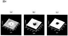
- the inventor scrutinizes the manufacturing process of the epitaxial wafer, and the SF generated after the epitaxial growth is generated starting from a micro pit (micro concave portion) existing on the wafer surface before the epitaxial growth (after pre-baking). I found.
- FIG. 4 shows the surface of a silicon crystal substrate after a polysilicon layer is formed on the back side of a silicon crystal substrate doped with phosphorus and germanium at a high concentration, and then prebaked in a hydrogen atmosphere as a pretreatment for epitaxial growth.
- FIG. 2 is a diagram showing typical micropits observed on the surface of a silicon crystal substrate when observing the film using an atomic force microscope (AFM).
- AFM atomic force microscope
- micro pits are not observed even when boron (B) is added at a high concentration as a p-type dopant and germanium is added to the silicon wafer, so that phosphorus is doped at a high concentration in the crystal of the wafer. Is likely to be involved.
- red phosphorus has a function of promoting oxygen precipitation
- the poly back seal formation process is performed at around 650 ° C., which is a temperature range where oxygen precipitation nuclei are formed in silicon crystals.
- minute oxygen precipitation nuclei are formed in the crystal in a large amount and minute pits are formed starting from the oxygen precipitation nuclei when subjected to high-temperature heat treatment of pre-baking.
- a complex (clustering) of oxygen precipitates and germanium is formed, and germanium sublimes at a relatively low temperature, so that the complex sublimates and jumps out of the wafer surface when subjected to pre-baking high-temperature heat treatment.
- the possibility that the part becomes a micro pit is also considered, but it is not clear yet.
- the present inventors formed a polysilicon layer on the back side of the silicon crystal substrate with respect to the silicon crystal substrate doped with phosphorus and germanium at a high concentration, and formed a silicon epitaxial layer on the surface of the silicon crystal substrate.
- An epitaxial silicon wafer on which a layer is grown is manufactured.
- FIG. 1 shows the number of LPDs on the surface of the wafer in the epitaxial silicon wafer manufacturing method when the PBS formation process is performed before and after the epitaxial growth process and when the PBS formation process is performed after the epitaxial growth process.
- the horizontal axis indicates the case where the PBS formation step is performed (with PBS) before the epitaxial growth process (process temperature 1100 ° C.), the case where only the heat treatment similar to the PBS formation step is performed (heat treatment only), and the PBS formation.
- Process temperature 1100 ° C. the case where only the heat treatment similar to the PBS formation step is performed (heat treatment only), and the PBS formation.
- Each wafer is shown when the process is not performed, and when the PBS formation process is performed after the epitaxial growth process (process temperature 1100 ° C.), and the vertical axis indicates the number of LPDs per wafer.
- the number of LPDs on the wafer surface shown on the vertical axis is measured in the DCN mode of SP-1 manufactured by KLA-Tencor, which is a particle counter, and is 0.13 ⁇ m or more in size. The number of results obtained by detecting and counting LPD is shown.
- the same heat treatment as the PBS formation process is performed (the same temperature condition (for example, 650 ° C., 4 hours)).
- the number of LPDs generated on the wafer can be reduced when the epitaxial growth process is performed without performing the PBS formation process before the epitaxial growth process, compared to the case where the source gas as the raw material is not supplied). For example, it can be 100 or less (32 or less per 100 cm 2 area on the wafer surface (surface of the silicon epitaxial layer)).
- each step has been reviewed so that the PBS formation step can be executed after the epitaxial growth step.
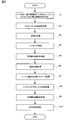
- FIG. 2 is a diagram showing a method for manufacturing an epitaxial silicon wafer according to an embodiment of the present invention.
- a silicon crystal substrate is prepared in which phosphorus and germanium are doped together at a high concentration during silicon crystal growth (step S1).
- One of its typical methods is to use a Czochralski method to pull a silicon single crystal ingot heavily doped with phosphorus and germanium from molten silicon heavily doped with phosphorus and germanium, and A silicon crystal substrate is manufactured from the silicon single crystal ingot by a known processing technique (cutting, grinding, polishing, cleaning, etching).
- the phosphorus concentration of the silicon crystal substrate is in the range of 4.7 ⁇ 10 19 to 9.47 ⁇ 10 19 atoms / cm 3
- the germanium concentration is 7.0 ⁇ 10 19 to 1.0 ⁇ 10. It is preferably in the range of 20 atoms / cm 3 .
- the electrical resistivity of the silicon crystal substrate doped with high-concentration phosphorus and germanium within the above range is in the range of 0.8 ⁇ 10 ⁇ 3 to 1.5 ⁇ 10 ⁇ 3 ⁇ ⁇ cm, This electrical resistivity satisfies the resistivity requirement required for a wafer for a power MOS transistor.
- the silicon crystal substrate is processed to a fixed size by performing lapping or surface grinding on the cut silicon crystal substrate (step S2), and chamfering the silicon crystal substrate (step S3).
- the chamfered portion may be mirror-polished, or step S3 may be performed before and after step S2.
- an etching process is performed to remove mechanical processing damage of the silicon crystal substrate (step S4), and an oxidation film is formed on the back surface of the silicon crystal substrate to prevent autodoping from the silicon crystal substrate.
- Film formation processing is performed (step S5), and the surface (one side or both sides) of the silicon crystal substrate is mirror-polished (step S6).
- the back surface oxide film forming process is, for example, a low temperature of 400 to 500 ° C. and a relatively short time of about 10 minutes. According to the processes up to step S6, the main surface (the surface on the side where the epitaxial layer is formed in this embodiment) is mirror-polished, the edge portion is chamfered, and the back surface (the surface opposite to the main surface) is oxidized. A silicon crystal substrate on which a film is formed is obtained.
- the silicon crystal substrate surface is cleaned at a high temperature for a short time for the purpose of cleaning the surface of the silicon crystal substrate (removal of natural oxide film and particles adhering to the substrate surface).
- the heat treatment is performed (step S7).
- the pre-bake treatment is performed in an atmosphere of hydrogen gas at 1150 to 1200 ° C. or an inert gas such as argon, and the pre-bake time is 35 seconds or longer (for example, the shortest 35 seconds).
- a treatment step (epitaxial growth step) for growing a silicon epitaxial layer on the silicon crystal substrate by a CVD method is performed (step S8).
- the process temperature of the epitaxial growth step is desirably in the range of 1000 to 1090 ° C., and more desirably in the range of 1050 to 1080 ° C. Note that the process temperature range of 1000 ° C. or lower is not practical. This is because at such a process temperature, the growth rate of the silicon epitaxial layer becomes slow and the quality deteriorates.
- a back surface oxide film removing process for removing the oxide film on the back surface of the silicon crystal substrate is executed (step S9), and a PBS forming step for forming a polysilicon layer is performed on the back surface side of the silicon crystal substrate ( Step S10).
- the PBS formation step can be performed, for example, by a reduced pressure chemical vapor deposition method using a normal vertical reactor.
- the source gas is SiH 4
- the pressure is 26.66 pa
- the generated film thickness is 0.1 ⁇ m or more.
- the film thickness generated from the viewpoint of productivity is preferably 2 ⁇ m or less.
- the process temperature in the PBS forming step can be set to 650 ° C., for example. In the present embodiment, since the epitaxial layer has already been formed, the influence of the PBS formation step on the generation of LPD in the epitaxial layer is hardly caused as in the prior art.
- a polysilicon layer is formed on the entire surface of the wafer, and a polishing process or an etching process is performed to remove the polysilicon layer formed on the wafer surface or the chamfered portion of the wafer.
- a wafer having a polysilicon layer formed on the back surface of the wafer is formed.
- the electrical resistivity of the silicon crystal substrate is very low within the range of 0.8 ⁇ 10 ⁇ 3 to 1.5 ⁇ 10 ⁇ 3 ⁇ ⁇ cm, and misfit dislocations in the silicon epitaxial layer are reduced.
- An epitaxial silicon wafer with a very small number of LPDs caused by SF (stacking fault) can be manufactured.
- LPD having a particle size of 0.13 ⁇ m or more is measured in the DCN mode of SP-1 manufactured by KLA-Tencor, 32 or less per 100 cm 2 on the wafer surface (surface of the silicon epitaxial layer) (200 mm diameter wafer)
- Epitaxial silicon that can be used for power MOS transistors such as 100 or less on the surface (314 cm 2 ), preferably about 0 to 3 per 100 cm 2 surface area of the wafer surface (10 or less on the surface of a 200 mm diameter wafer) A wafer is manufactured.
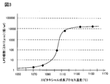
- FIG. 3 is a diagram showing the relationship between the process temperature of the epitaxial growth step according to an embodiment of the present invention and the number of LPDs on the surface of the wafer.
- the experiment was performed by changing the process temperature (epitaxial growth actual temperature) of the epitaxial growth step.
- 3 shows the relationship between the process temperature of the epitaxial growth step and the number of LPDs that appear on the wafer surface due to SF.
- the horizontal axis indicates the process temperature of the epitaxial growth step, and the vertical axis indicates the number of LPDs on the wafer surface per wafer.
- the number of LPDs per wafer indicated on the vertical axis is the number of results obtained by detecting and counting LPDs having a size of 0.13 ⁇ m or more, measured in the DCN mode of SP-1 manufactured by KLA-Tencor. Is shown.
- a silicon crystal substrate having a diameter of 200 mm in which phosphorus and germanium are doped together in the above-described concentration range at the time of silicon crystal growth was used.
- a silicon epitaxial layer was formed on 25 silicon crystal substrates for each process temperature.
- the number of LPDs at each process temperature shown in FIG. 3 is an average value of the number of LPDs of those 25 wafers.
- the process temperature range can be broadly divided into a range of 1110 ° C. or higher, a range of 1110 to 1090 ° C., and a range of 1090 ° C. or lower (however, 1000 ° C. or higher).
- the number of LPDs is as large as 10,000 or more.
- the number of LPDs rapidly decreases in the range of 1110 to 1090 ° C.
- the number of LPDs is as small as about 100 or less (32 or less per 100 cm 2 of the wafer surface area) even if it is a large number.
- the process temperature during epitaxial growth is preferably 1100 ° C. or less, and more preferably in the range of 1000 ° C. to 1090 ° C.
- the above problems occur when the number of LPDs is very few (about 2 to 0 per 100 cm 2 of the wafer surface area) and the process temperature is 1000 ° C. or less. Therefore, it can be said to be the optimum process temperature range.
Landscapes
- Engineering & Computer Science (AREA)
- Physics & Mathematics (AREA)
- Condensed Matter Physics & Semiconductors (AREA)
- General Physics & Mathematics (AREA)
- Manufacturing & Machinery (AREA)
- Computer Hardware Design (AREA)
- Microelectronics & Electronic Packaging (AREA)
- Power Engineering (AREA)
- Chemical & Material Sciences (AREA)
- Materials Engineering (AREA)
- Recrystallisation Techniques (AREA)
- Chemical Vapour Deposition (AREA)
Priority Applications (2)
| Application Number | Priority Date | Filing Date | Title |
|---|---|---|---|
| DE112010002747.1T DE112010002747B4 (de) | 2009-06-29 | 2010-05-28 | Verfahren zur Herstellung eines Siliziumepitaxialwafers |
| US13/378,562 US8659020B2 (en) | 2009-06-29 | 2010-05-28 | Epitaxial silicon wafer and method for manufacturing same |
Applications Claiming Priority (2)
| Application Number | Priority Date | Filing Date | Title |
|---|---|---|---|
| JP2009-153496 | 2009-06-29 | ||
| JP2009153496A JP5609025B2 (ja) | 2009-06-29 | 2009-06-29 | エピタキシャルシリコンウェーハの製造方法 |
Publications (1)
| Publication Number | Publication Date |
|---|---|
| WO2011001770A1 true WO2011001770A1 (ja) | 2011-01-06 |
Family
ID=43410851
Family Applications (1)
| Application Number | Title | Priority Date | Filing Date |
|---|---|---|---|
| PCT/JP2010/059089 Ceased WO2011001770A1 (ja) | 2009-06-29 | 2010-05-28 | エピタキシャルシリコンウェーハとその製造方法 |
Country Status (4)
| Country | Link |
|---|---|
| US (1) | US8659020B2 (enExample) |
| JP (1) | JP5609025B2 (enExample) |
| DE (1) | DE112010002747B4 (enExample) |
| WO (1) | WO2011001770A1 (enExample) |
Cited By (2)
| Publication number | Priority date | Publication date | Assignee | Title |
|---|---|---|---|---|
| JP2011044505A (ja) * | 2009-08-19 | 2011-03-03 | Shin Etsu Handotai Co Ltd | シリコンエピタキシャルウェーハの製造方法 |
| CN109075039A (zh) * | 2016-04-20 | 2018-12-21 | 信越半导体株式会社 | 外延晶片的制造方法 |
Families Citing this family (3)
| Publication number | Priority date | Publication date | Assignee | Title |
|---|---|---|---|---|
| JP6009237B2 (ja) * | 2012-06-18 | 2016-10-19 | Sumco Techxiv株式会社 | エピタキシャルシリコンウェーハの製造方法、および、エピタキシャルシリコンウェーハ |
| JP5845143B2 (ja) | 2012-06-29 | 2016-01-20 | 株式会社Sumco | エピタキシャルシリコンウェーハの製造方法、および、エピタキシャルシリコンウェーハ |
| US10233562B2 (en) * | 2013-04-24 | 2019-03-19 | Sumco Techxiv Corporation | Method for producing single crystal, and method for producing silicon wafer |
Citations (4)
| Publication number | Priority date | Publication date | Assignee | Title |
|---|---|---|---|---|
| JPH10172976A (ja) * | 1996-12-12 | 1998-06-26 | Mitsubishi Materials Shilicon Corp | Eg層付きエピタキシャルウェーハの製造方法 |
| JP2001167995A (ja) * | 1999-09-29 | 2001-06-22 | Mimasu Semiconductor Industry Co Ltd | ウェーハ、エピタキシャルウェーハ及びそれらの製造方法 |
| JP2003188107A (ja) * | 2001-12-19 | 2003-07-04 | Shin Etsu Handotai Co Ltd | 半導体エピタキシャルウエーハの製造方法および半導体エピタキシャルウエーハ |
| WO2008146725A1 (ja) * | 2007-05-31 | 2008-12-04 | Sumco Techxiv Corporation | シリコン単結晶の製造方法及びn型高ドープ半導体基板 |
Family Cites Families (9)
| Publication number | Priority date | Publication date | Assignee | Title |
|---|---|---|---|---|
| US5553566A (en) | 1995-06-22 | 1996-09-10 | Motorola Inc. | Method of eliminating dislocations and lowering lattice strain for highly doped N+ substrates |
| JPH10223641A (ja) | 1996-12-03 | 1998-08-21 | Sumitomo Sitix Corp | 半導体シリコンエピタキシャルウェーハ及び半導体デバイスの製造方法 |
| JP2000031153A (ja) | 1998-07-13 | 2000-01-28 | Shin Etsu Handotai Co Ltd | Siウエーハ及びその製造方法 |
| JP4442955B2 (ja) * | 1999-07-28 | 2010-03-31 | 株式会社Sumco | エピタキシャルウェーハの製造方法 |
| US8273146B1 (en) | 1999-09-29 | 2012-09-25 | Shin-Etsu Handotai Co., Ltd. | Wafer and epitaxial wafer, and manufacturing processes therefor |
| JP2006073580A (ja) * | 2004-08-31 | 2006-03-16 | Sumco Corp | シリコンエピタキシャルウェーハ及びその製造方法 |
| US20090004458A1 (en) * | 2007-06-29 | 2009-01-01 | Memc Electronic Materials, Inc. | Diffusion Control in Heavily Doped Substrates |
| JP5509581B2 (ja) * | 2008-11-27 | 2014-06-04 | 信越半導体株式会社 | 半導体ウェーハの評価方法 |
| JP5246065B2 (ja) * | 2009-06-29 | 2013-07-24 | 株式会社Sumco | エピタキシャルシリコンウェーハとその製造方法 |
-
2009
- 2009-06-29 JP JP2009153496A patent/JP5609025B2/ja active Active
-
2010
- 2010-05-28 DE DE112010002747.1T patent/DE112010002747B4/de active Active
- 2010-05-28 WO PCT/JP2010/059089 patent/WO2011001770A1/ja not_active Ceased
- 2010-05-28 US US13/378,562 patent/US8659020B2/en active Active
Patent Citations (4)
| Publication number | Priority date | Publication date | Assignee | Title |
|---|---|---|---|---|
| JPH10172976A (ja) * | 1996-12-12 | 1998-06-26 | Mitsubishi Materials Shilicon Corp | Eg層付きエピタキシャルウェーハの製造方法 |
| JP2001167995A (ja) * | 1999-09-29 | 2001-06-22 | Mimasu Semiconductor Industry Co Ltd | ウェーハ、エピタキシャルウェーハ及びそれらの製造方法 |
| JP2003188107A (ja) * | 2001-12-19 | 2003-07-04 | Shin Etsu Handotai Co Ltd | 半導体エピタキシャルウエーハの製造方法および半導体エピタキシャルウエーハ |
| WO2008146725A1 (ja) * | 2007-05-31 | 2008-12-04 | Sumco Techxiv Corporation | シリコン単結晶の製造方法及びn型高ドープ半導体基板 |
Cited By (3)
| Publication number | Priority date | Publication date | Assignee | Title |
|---|---|---|---|---|
| JP2011044505A (ja) * | 2009-08-19 | 2011-03-03 | Shin Etsu Handotai Co Ltd | シリコンエピタキシャルウェーハの製造方法 |
| CN109075039A (zh) * | 2016-04-20 | 2018-12-21 | 信越半导体株式会社 | 外延晶片的制造方法 |
| CN109075039B (zh) * | 2016-04-20 | 2023-06-09 | 信越半导体株式会社 | 外延晶片的制造方法 |
Also Published As
| Publication number | Publication date |
|---|---|
| JP5609025B2 (ja) | 2014-10-22 |
| DE112010002747T5 (de) | 2013-09-26 |
| US8659020B2 (en) | 2014-02-25 |
| DE112010002747B4 (de) | 2020-12-24 |
| US20120112190A1 (en) | 2012-05-10 |
| JP2011009614A (ja) | 2011-01-13 |
Similar Documents
| Publication | Publication Date | Title |
|---|---|---|
| CN107533959B (zh) | 外延硅晶片的制造方法 | |
| JP3988307B2 (ja) | シリコン単結晶、シリコンウェーハ及びエピタキシャルウェーハ | |
| JP5533869B2 (ja) | エピタキシャルシリコンウェーハとその製造方法 | |
| JP5246065B2 (ja) | エピタキシャルシリコンウェーハとその製造方法 | |
| JP5609025B2 (ja) | エピタキシャルシリコンウェーハの製造方法 | |
| JP5463693B2 (ja) | シリコンエピタキシャルウェーハの製造方法 | |
| JP2025146998A (ja) | シリコンウェーハおよびエピタキシャルシリコンウェーハ | |
| TWI741950B (zh) | 矽晶圓的製造方法 | |
| JP5803722B2 (ja) | シリコンエピタキシャルウェーハの製造方法 | |
| JP5338559B2 (ja) | シリコンエピタキシャルウェーハの製造方法 | |
| JP2010153631A (ja) | エピタキシャルシリコンウェーハとその製造方法 | |
| WO2010131412A1 (ja) | シリコンウェーハおよびその製造方法 | |
| JPH11204534A (ja) | シリコンエピタキシャルウェーハの製造方法 | |
| JP7757917B2 (ja) | シリコンウェーハおよびエピタキシャルシリコンウェーハ | |
| JP5672021B2 (ja) | 半導体基板の製造方法 | |
| JP7775800B2 (ja) | シリコンウェーハおよびエピタキシャルシリコンウェーハ | |
| JP7658332B2 (ja) | シリコンウェーハおよびエピタキシャルシリコンウェーハ | |
| KR102847759B1 (ko) | 실리콘 웨이퍼 및 에피택셜 실리콘 웨이퍼 | |
| KR102858653B1 (ko) | 실리콘 웨이퍼 및 에피택셜 실리콘 웨이퍼 | |
| JP6372709B2 (ja) | エピタキシャルウェーハの製造方法 |
Legal Events
| Date | Code | Title | Description |
|---|---|---|---|
| 121 | Ep: the epo has been informed by wipo that ep was designated in this application |
Ref document number: 10793941 Country of ref document: EP Kind code of ref document: A1 |
|
| WWE | Wipo information: entry into national phase |
Ref document number: 13378562 Country of ref document: US |
|
| WWE | Wipo information: entry into national phase |
Ref document number: 112010002747 Country of ref document: DE Ref document number: 1120100027471 Country of ref document: DE |
|
| 122 | Ep: pct application non-entry in european phase |
Ref document number: 10793941 Country of ref document: EP Kind code of ref document: A1 |