例えば、パワーMOSトランジスタ用のエピタキシャルシリコンウェーハには、そのシリコン結晶基板の電気抵抗率が非常に低いことが要求される。シリコン結晶基板の電気抵抗率を十分に低くするために、ウェーハの素材であるシリコン結晶インゴットの引き上げ工程で(すなわち、シリコン結晶の育成時に)、溶融シリコンに抵抗率調整用のn型ドーパントとして砒素(As)やアンチモン(Sb)をドープする技術が知られている。しかし、これらのドーパントは非常に蒸発しやすいので、シリコン結晶中のドーパント濃度を十分に高くすることが難しく、要求される程度に低い抵抗率をもつシリコン結晶基板を製造することが難しい。
For example, an epitaxial silicon wafer for a power MOS transistor is required to have a very low electrical resistivity of the silicon crystal substrate. In order to sufficiently reduce the electrical resistivity of the silicon crystal substrate, arsenic is used as an n-type dopant for adjusting the resistivity in the molten silicon in the pulling process of the silicon crystal ingot that is the material of the wafer (that is, when growing the silicon crystal). A technique for doping (As) or antimony (Sb) is known. However, since these dopants are very easy to evaporate, it is difficult to make the dopant concentration in the silicon crystal sufficiently high, and it is difficult to manufacture a silicon crystal substrate having a resistivity as low as required.
そこで、揮発性の低い性質をもつn型ドーパントとしてリン(P)を高濃度にドープした電気抵抗率が非常に低いシリコン結晶基板が使用されつつある。
Therefore, a silicon crystal substrate having a very low electrical resistivity doped with phosphorus (P) at a high concentration is being used as an n-type dopant having low volatile properties.
ところが、高濃度にリンがドープされたシリコン結晶基板上にシリコンのエピタキシャル層を形成すると、シリコン結晶基板とシリコンエピタキシャル層との界面部分でのリンの濃度差に起因する転位欠陥(ミスフィット転位)が発生するという問題がある。ミスフィット転位は、シリコン結晶基板の界面部分からシリコンエピタキシャル層の表面にまで伝播し、目視で細長く薄いラインが密集したものとして観測され、半導体素子の電気的性能を低下させる原因となる。ミスフィット転位の原因は、シリコンの原子半径が1.17Å(オングストローム)であるのに対して、リンの原子半径はシリコンよりかなり小さい1.10Åであり、このような両者の共有結合半径の大きな相違が結晶内に無用な歪を生じさせることにある(因みに、砒素の原子半径は、シリコンにかなり近い1.18Åであるため、ミスフィット転位は非常に少ない)。
However, when a silicon epitaxial layer is formed on a silicon crystal substrate doped with phosphorus at a high concentration, dislocation defects (misfit dislocations) are caused by a difference in phosphorus concentration at the interface between the silicon crystal substrate and the silicon epitaxial layer. There is a problem that occurs. Misfit dislocations propagate from the interface portion of the silicon crystal substrate to the surface of the silicon epitaxial layer, and are visually observed as densely packed thin and thin lines, causing a reduction in the electrical performance of the semiconductor element. The cause of the misfit dislocation is that the atomic radius of silicon is 1.17 Å (angstrom), whereas the atomic radius of phosphorus is 1.10 か な り, which is considerably smaller than that of silicon. The difference is that it causes unwanted strain in the crystal (by the way, the atomic radius of arsenic is 1.18Å which is quite close to silicon, so there are very few misfit dislocations).
この問題を解決するために、シリコン単結晶インゴット引き上げ工程において、原子半径がシリコンより大きい1.22Åであるゲルマニウム(Ge)をリンと同時にドーピングすることにより、リンによって生じたシリコン結晶格子の歪をゲルマニウムで緩和して、ミスフィット転位の発生を抑制する技術が知られている(特許文献1参照)。
In order to solve this problem, in the silicon single crystal ingot pulling process, germanium (Ge) having an atomic radius of 1.22 mm larger than that of silicon is doped at the same time as phosphorus, thereby reducing the distortion of the silicon crystal lattice caused by phosphorus. A technique is known that relaxes with germanium and suppresses the occurrence of misfit dislocations (see Patent Document 1).
エピタキシャルウェーハは、高温でエピタキシャル成長が行なわれるために、シリコン単結晶インゴットの育成段階で結晶内に形成された酸素析出物(BMD)や酸素析出核などが高温熱処理によって消滅してしまい、ゲッタリング能力が低いという問題がある。
Since epitaxial wafers are epitaxially grown at high temperatures, oxygen precipitates (BMD) and oxygen precipitation nuclei formed in the crystal during the growth of the silicon single crystal ingot disappear due to high-temperature heat treatment, resulting in gettering capability. There is a problem that is low.
ゲッタリング不足を解消するための対策としてのゲッタリング方法としては、IG(イントリンシックゲッタリング)法や、EG(エクストリンシックゲッタリング)法が知られている(非特許文献1参照)。
IG (intrinsic gettering) method and EG (extrinsic gettering) method are known as a gettering method as a measure for solving insufficient gettering (see Non-Patent Document 1).
例えば、ウェーハに対して酸素析出核形成熱処理を行って、酸素析出核密度を増大させた後、エピタキシャル成長を行う技術が知られている(特許文献2参照)。
For example, a technique is known in which oxygen precipitation nucleation heat treatment is performed on a wafer to increase the density of oxygen precipitation nuclei, and then epitaxial growth is performed (see Patent Document 2).
また、ウェーハの裏面にポリシリコン層を形成させて、基板との界面等にできる歪み場や格子不整合を利用するEG法の一例としてのポリバックシール(PBS)法が、エピタキシャル成長処理前に行う技術が知られている(特許文献3、特許文献4参照)。
Further, a poly back seal (PBS) method, which is an example of an EG method using a strain field or lattice mismatch that can be formed at the interface with the substrate by forming a polysilicon layer on the back surface of the wafer, is performed before the epitaxial growth process. Techniques are known (see Patent Document 3 and Patent Document 4).
以下、本発明に係るエピタキシャルシリコンウェーハの製造方法について詳細に説明する。
Hereinafter, the method for producing an epitaxial silicon wafer according to the present invention will be described in detail.
従来技術では、前述したとおり、シリコン結晶育成時にリン(P)とゲルマニウム(Ge)がドープされた(特に、パワーMOSトランジスタ用に要求されるような非常に低い電気抵抗率を実現できる程度の高濃度にリンとゲルマニウムがドープされた)シリコン結晶基板の裏面側にポリシリコン層を形成させた後(ポリバックシール形成処理(PBS形成処理)後)に、シリコン結晶基板の表面上にシリコンエピタキシャル層を成長させると、そのシリコンエピタキシャル層に多数のSF(スタッキングフォルト)が発生する。
In the prior art, as described above, phosphorus (P) and germanium (Ge) are doped at the time of silicon crystal growth (particularly high enough to realize a very low electrical resistivity as required for power MOS transistors). After forming a polysilicon layer on the back side of the silicon crystal substrate (doped with phosphorus and germanium in concentration) (after poly back seal formation processing (PBS formation processing)), a silicon epitaxial layer on the surface of the silicon crystal substrate As a result, a large number of SFs (stacking faults) are generated in the silicon epitaxial layer.
発明者は、エピタキシャルウェーハの製造工程を精査することにより、エピタキシャル成長後に発生しているSFは、エピタキシャル成長前(プリベーク後)のウェーハ表面に存在する微小ピット(微小凹部)を起点に発生していることを見出した。
The inventor scrutinizes the manufacturing process of the epitaxial wafer, and the SF generated after the epitaxial growth is generated starting from a micro pit (micro concave portion) existing on the wafer surface before the epitaxial growth (after pre-baking). I found.
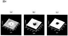
図4は、リンとゲルマニウムを高濃度にドープしたシリコン結晶基板の裏面側にポリシリコン層を形成させた後に、エピタキシャル成長の前処理としてシリコンウェーハを水素雰囲気中でプリベークした後、シリコン結晶基板の表面を原子間力顕微鏡(AFM)を用いて観察したときに、シリコン結晶基板の表面上で観察された代表的な微小ピットの様子を示す図である。
FIG. 4 shows the surface of a silicon crystal substrate after a polysilicon layer is formed on the back side of a silicon crystal substrate doped with phosphorus and germanium at a high concentration, and then prebaked in a hydrogen atmosphere as a pretreatment for epitaxial growth. FIG. 2 is a diagram showing typical micropits observed on the surface of a silicon crystal substrate when observing the film using an atomic force microscope (AFM).
この微小ピットは、p型ドーパントとしてボロン(B)を高濃度に添加し、かつゲルマニウムを添加したシリコンウェーハにプリベーク処理を施しても観察されないことから、ウェーハの結晶内に高濃度にドープしたリンが関与している可能性が高いと考えられる。
These micro pits are not observed even when boron (B) is added at a high concentration as a p-type dopant and germanium is added to the silicon wafer, so that phosphorus is doped at a high concentration in the crystal of the wafer. Is likely to be involved.
例えば、赤燐は酸素析出を促進させる働きがあることが確認されてきており、ポリバックシール形成処理がシリコン結晶内に酸素析出核が形成される温度域である650℃前後で行なわれることから、結晶内に微小な酸素析出核が多量に形成され、プリベークの高温熱処理を受けた際に、酸素析出核を起点に微小ピットが形成されているという可能性が高い。また、酸素析出物とゲルマニウムとの複合体(クラスター化)が形成され、ゲルマニウムが比較的低温で昇華するために、プリベークの高温熱処理を受けた際に、複合体が昇華してウェーハ表面から飛び出し、当該部分が微小ピットとなるという可能性も考えられるが、まだ明確ではない。
For example, it has been confirmed that red phosphorus has a function of promoting oxygen precipitation, and the poly back seal formation process is performed at around 650 ° C., which is a temperature range where oxygen precipitation nuclei are formed in silicon crystals. There is a high possibility that minute oxygen precipitation nuclei are formed in the crystal in a large amount and minute pits are formed starting from the oxygen precipitation nuclei when subjected to high-temperature heat treatment of pre-baking. In addition, a complex (clustering) of oxygen precipitates and germanium is formed, and germanium sublimes at a relatively low temperature, so that the complex sublimates and jumps out of the wafer surface when subjected to pre-baking high-temperature heat treatment. The possibility that the part becomes a micro pit is also considered, but it is not clear yet.
そこで、本発明者等は、リンとゲルマニウムが高濃度にドープされたシリコン結晶基板に対して、シリコン結晶基板の裏面側にポリシリコン層を形成し、また、シリコン結晶基板の表面上にシリコンエピタキシャル層の成長を行うエピタキシャルシリコンウェーハを製造するものであって、ポリシリコン層を形成する処理を行う工程(PBS形成工程)によるLPDの増加への影響を実験することにより、PBS形成工程の適切な実行順序を見出すとともに、エピタキシャル成長を行わせる工程(エピタキシャル成長工程)における条件を種々に変更しながら実験を積み重ねた結果、ミスフィット転位を抑制しながら、さらにSFの発生をも抑制することができる最適なエピタキシャル成長工程の条件が存在することを見出した。
Therefore, the present inventors formed a polysilicon layer on the back side of the silicon crystal substrate with respect to the silicon crystal substrate doped with phosphorus and germanium at a high concentration, and formed a silicon epitaxial layer on the surface of the silicon crystal substrate. An epitaxial silicon wafer on which a layer is grown is manufactured. By examining the influence on the increase in LPD by the process of forming a polysilicon layer (PBS forming process), it is possible to As a result of accumulating experiments while finding out the order of execution and changing the conditions in the process of epitaxial growth (epitaxial growth process) in various ways, it is optimal to suppress the occurrence of SF while suppressing misfit dislocations. It has been found that there are conditions for the epitaxial growth process.
図1は、エピタキシャルシリコンウェーハの製造方法において、エピタキシャル成長処理前にPBS形成工程を行った場合と行わなかった場合と、エピタキシャル成長処理後にPBS形成工程を行った場合、それぞれにおけるウェーハの表面上のLPD個数との関係を示す図である。同図において、横軸は、エピタキシャル成長処理(プロセス温度1100℃)前に、PBS形成工程を行った場合(PBS有)、PBS形成工程と同様な熱処理のみを行った場合(熱処理のみ)、PBS形成工程を行わなかった場合、およびエピタキシャル成長処理(プロセス温度1100℃)後にPBS形成工程を行った場合における各ウェーハを示し、縦軸は、ウェーハ1枚当りのLPD個数を示している。
FIG. 1 shows the number of LPDs on the surface of the wafer in the epitaxial silicon wafer manufacturing method when the PBS formation process is performed before and after the epitaxial growth process and when the PBS formation process is performed after the epitaxial growth process. It is a figure which shows the relationship. In the figure, the horizontal axis indicates the case where the PBS formation step is performed (with PBS) before the epitaxial growth process (process temperature 1100 ° C.), the case where only the heat treatment similar to the PBS formation step is performed (heat treatment only), and the PBS formation. Each wafer is shown when the process is not performed, and when the PBS formation process is performed after the epitaxial growth process (process temperature 1100 ° C.), and the vertical axis indicates the number of LPDs per wafer.
ここで、縦軸に示されたウェーハ1枚当りのウェーハ表面のLPD個数は、パーティクルカウンターであるKLA-Tencor社製SP-1のDCNモードで測定したものであり、0.13μmサイズ以上であるLPDを検出して計数した結果の個数を示している。
Here, the number of LPDs on the wafer surface shown on the vertical axis is measured in the DCN mode of SP-1 manufactured by KLA-Tencor, which is a particle counter, and is 0.13 μm or more in size. The number of results obtained by detecting and counting LPD is shown.
図1からわかるように、エピタキシャル成長処理前に、PBS形成工程を行った場合、PBS形成工程と同様な熱処理を行った場合(同じ温度条件(例えば、650℃、4時間)で、ポリシリコン層の原料となる原料ガスを供給しなかった場合)に比して、エピタキシャル成長処理前に、PBS形成工程を行なわずに、エピタキシャル成長工程を行った場合のほうが、ウェーハに発生するLPDの数を低減でき、例えば、100個以下(ウェーハ表面(シリコンエピタキシャル層の表面)における面積100cm2当たり32個以下)にすることができる。
As can be seen from FIG. 1, when the PBS formation process is performed before the epitaxial growth process, the same heat treatment as the PBS formation process is performed (the same temperature condition (for example, 650 ° C., 4 hours)). The number of LPDs generated on the wafer can be reduced when the epitaxial growth process is performed without performing the PBS formation process before the epitaxial growth process, compared to the case where the source gas as the raw material is not supplied). For example, it can be 100 or less (32 or less per 100 cm 2 area on the wafer surface (surface of the silicon epitaxial layer)).
そこで、本実施形態においては、エピタキシャルシリコンウェーハの製造方法において、PBS形成工程を、エピタキシャル成長工程よりも後に実行できるように各工程を見直した。
Therefore, in the present embodiment, in the method for manufacturing an epitaxial silicon wafer, each step has been reviewed so that the PBS formation step can be executed after the epitaxial growth step.
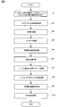
図2は、本発明の一実施形態に係るエピタキシャルシリコンウェーハの製造方法を示す図である。
FIG. 2 is a diagram showing a method for manufacturing an epitaxial silicon wafer according to an embodiment of the present invention.
先ず、シリコン結晶育成時にリンとゲルマニウムが一緒に高濃度にドープされたシリコン結晶基板を用意する(ステップS1)。その典型的な方法の一つは、リンとゲルマニウムが高濃度にドープされた溶融シリコンから、チョクラルスキー法を用いて、リンとゲルマニウムが高濃度にドープされたシリコン単結晶インゴットを引き上げ、そして、そのシリコン単結晶インゴットから公知の加工技術(切断、研削、研磨、洗浄、エッチング)によりシリコン結晶基板を製作する、という方法である。
First, a silicon crystal substrate is prepared in which phosphorus and germanium are doped together at a high concentration during silicon crystal growth (step S1). One of its typical methods is to use a Czochralski method to pull a silicon single crystal ingot heavily doped with phosphorus and germanium from molten silicon heavily doped with phosphorus and germanium, and A silicon crystal substrate is manufactured from the silicon single crystal ingot by a known processing technique (cutting, grinding, polishing, cleaning, etching).
ここで、シリコン結晶基板のリンの濃度は4.7×10¹⁹~9.47×10¹⁹atoms/cm3の範囲内であり、ゲルマニウムの濃度が7.0×1019~1.0×1020atoms/cm3の範囲内であることが好ましい。シリコン結晶基板の素材であるシリコンインゴットの引き上げプロセスにおいて、インゴットが引き上げられる元の溶融シリコンにリンとゲルマニウムを同時にドープするときのそれぞれの濃度を調整することにより、上記のような範囲内で高濃度のリンとゲルマニウムを含んだシリコン結晶基板を得ることができる。上記のような範囲内の高濃度のリンとゲルマニウムとがドープされたシリコン結晶基板の電気抵抗率は0.8×10-3~1.5×10-3Ω・cmの範囲内であり、この電気抵抗率は、パワーMOSトランジスタ用のウェーハに要求される抵抗率条件を満たすものである。
Here, the phosphorus concentration of the silicon crystal substrate is in the range of 4.7 × 10 19 to 9.47 × 10 19 atoms / cm 3 , and the germanium concentration is 7.0 × 10 19 to 1.0 × 10. It is preferably in the range of 20 atoms / cm 3 . In the pulling process of the silicon ingot that is the material of the silicon crystal substrate, by adjusting the respective concentrations when simultaneously doping phosphorus and germanium into the original molten silicon from which the ingot is pulled, the high concentration within the above range A silicon crystal substrate containing phosphorus and germanium can be obtained. The electrical resistivity of the silicon crystal substrate doped with high-concentration phosphorus and germanium within the above range is in the range of 0.8 × 10 −3 to 1.5 × 10 −3 Ω · cm, This electrical resistivity satisfies the resistivity requirement required for a wafer for a power MOS transistor.
リンとともにドープされたゲルマニウムの作用で、シリコンエピタキシャル層を成長させたときのミスフィット転位の発生が抑止される。
The generation of misfit dislocations when the silicon epitaxial layer is grown is suppressed by the action of germanium doped with phosphorus.
次に、切り出したシリコン結晶基板に対して、ラッピング又は平面研削処理を行うことによって、シリコン結晶基板を定寸に加工し(ステップS2)、シリコン結晶基板の面取り処理を行う(ステップS3)。なお、面取り処理後に、面取りを行なった部分(面取り部)を鏡面研磨してもよく、ステップS2の前後でステップS3を実施するようにしてもよい。
Next, the silicon crystal substrate is processed to a fixed size by performing lapping or surface grinding on the cut silicon crystal substrate (step S2), and chamfering the silicon crystal substrate (step S3). Note that after the chamfering process, the chamfered portion (chamfered portion) may be mirror-polished, or step S3 may be performed before and after step S2.
次に、シリコン結晶基板の機械的加工のダメージを除去するためエッチング処理を行い(ステップS4)、シリコン結晶基板からのオートドープ防止のために、シリコン結晶基板の裏面に酸化膜を形成する裏面酸化膜形成処理を行い(ステップS5)、シリコン結晶基板の表面(片面又は両面)を鏡面研磨加工する(ステップS6)。裏面酸化膜形成処理は、例えば、400~500℃の低い温度で、10分程度の比較的短時間であるので、シリコン結晶基板におけるLPDの発生への影響が少ない。ステップS6までの工程によると、主面(本実施形態では、エピタキシャル層が形成される側の面)が鏡面研磨され、エッジ部が面取りされ、裏面(主面と反対側の面)側に酸化膜が形成されたシリコン結晶基板が得られることとなる。
Next, an etching process is performed to remove mechanical processing damage of the silicon crystal substrate (step S4), and an oxidation film is formed on the back surface of the silicon crystal substrate to prevent autodoping from the silicon crystal substrate. Film formation processing is performed (step S5), and the surface (one side or both sides) of the silicon crystal substrate is mirror-polished (step S6). The back surface oxide film forming process is, for example, a low temperature of 400 to 500 ° C. and a relatively short time of about 10 minutes. According to the processes up to step S6, the main surface (the surface on the side where the epitaxial layer is formed in this embodiment) is mirror-polished, the edge portion is chamfered, and the back surface (the surface opposite to the main surface) is oxidized. A silicon crystal substrate on which a film is formed is obtained.
次に、シリコン結晶基板へのエピタキシャル層の形成に先立ち、シリコン結晶基板表面の清浄化(基板表面に付着する自然酸化膜、パーティクルの除去)を目的に、シリコン結晶基板に対して高温・短時間の熱処理(プリベーク)が行われる(ステップS7)。ここで、望ましくは、プリベーク処理は、1150~1200℃の水素ガス、又はアルゴンのような不活性ガス、の雰囲気中で行われ、プリベーク時間は35秒以上(例えば最短の35秒)である。
Next, prior to the formation of the epitaxial layer on the silicon crystal substrate, the silicon crystal substrate surface is cleaned at a high temperature for a short time for the purpose of cleaning the surface of the silicon crystal substrate (removal of natural oxide film and particles adhering to the substrate surface). The heat treatment (pre-bake) is performed (step S7). Here, preferably, the pre-bake treatment is performed in an atmosphere of hydrogen gas at 1150 to 1200 ° C. or an inert gas such as argon, and the pre-bake time is 35 seconds or longer (for example, the shortest 35 seconds).
プリベーク処理の後に、CVD法によりシリコン結晶基板上にシリコンエピタキシャル層を成長させる処理工程(エピタキシャル成長工程)が実行される(ステップS8)。ここで、エピタキシャル成長工程のプロセス温度は、1000~1090℃の範囲内が望ましく、より望ましくは、1050~1080℃の範囲内である。尚、プロセス温度の1000℃以下の範囲は実用的でない。そのようなプロセス温度では、シリコンエピタキシャル層の成長速度が遅くなるとともに品質が劣化するからである。
After the pre-bake treatment, a treatment step (epitaxial growth step) for growing a silicon epitaxial layer on the silicon crystal substrate by a CVD method is performed (step S8). Here, the process temperature of the epitaxial growth step is desirably in the range of 1000 to 1090 ° C., and more desirably in the range of 1050 to 1080 ° C. Note that the process temperature range of 1000 ° C. or lower is not practical. This is because at such a process temperature, the growth rate of the silicon epitaxial layer becomes slow and the quality deteriorates.
次に、シリコン結晶基板の裏面の酸化膜を除去する裏面酸化膜除去処理を実行し(ステップS9)、シリコン結晶基板の裏面側に対して、ポリシリコン層を形成するPBS形成工程が行われる(ステップS10)。
Next, a back surface oxide film removing process for removing the oxide film on the back surface of the silicon crystal substrate is executed (step S9), and a PBS forming step for forming a polysilicon layer is performed on the back surface side of the silicon crystal substrate ( Step S10).
PBS形成工程は、例えば、通常の縦型反応炉を用いて減圧化学気相成長法により行うことができる。PBS形成工程においては、例えば、原料ガスをSiH4とし、圧力26.66paとし、生成する膜厚としては、0.1μm以上としている。なお、生産性の観点から生成する膜厚は、2μm以下が好ましい。PBS形成工程におけるプロセス温度は、例えば、650℃とすることができる。本実施形態では、既にエピタキシャル層を形成しているために、従来のようにPBS形成工程による影響がエピタキシャル層のLPDの発生に与える影響がほとんどない。本実施形態では、PBS形成工程において、ウェーハの全面にポリシリコン層を形成し、研磨処理・エッチング処理などを行って、ウェーハの表面やウェーハの面取り部に形成されたポリシリコン層を除去することにより、ウェーハの裏面にポリシリコン層が形成されたウェーハを形成している。
The PBS formation step can be performed, for example, by a reduced pressure chemical vapor deposition method using a normal vertical reactor. In the PBS formation step, for example, the source gas is SiH 4 , the pressure is 26.66 pa, and the generated film thickness is 0.1 μm or more. The film thickness generated from the viewpoint of productivity is preferably 2 μm or less. The process temperature in the PBS forming step can be set to 650 ° C., for example. In the present embodiment, since the epitaxial layer has already been formed, the influence of the PBS formation step on the generation of LPD in the epitaxial layer is hardly caused as in the prior art. In this embodiment, in the PBS forming process, a polysilicon layer is formed on the entire surface of the wafer, and a polishing process or an etching process is performed to remove the polysilicon layer formed on the wafer surface or the chamfered portion of the wafer. Thus, a wafer having a polysilicon layer formed on the back surface of the wafer is formed.
以上の製造プロセスにより、シリコン結晶基板の電気抵抗率が0.8×10⁻³~1.5×10⁻³Ω・cmの範囲内で非常に低く、かつ、シリコンエピタキシャル層のミスフィット転位が極めて少なく、かつ、SF(スタッキングフォルト)に起因するLPDの個数が少ないエピタキシャルシリコンウェーハを製造することができる。例えば、KLA-Tencor社製SP-1のDCNモードで粒径0.13μmサイズ以上のLPDを測定した場合、ウェーハ表面(シリコンエピタキシャル層の表面)における面積100cm2当たり32個以下(直径200mmウェーハの表面(314cm2)において、100個以下)、好ましくはウェーハ表面の表面積100cm2当たり0~3個程度(直径200mmウェーハの表面において、10個以下)、という、パワーMOSトランジスタ用として利用できるエピタキシャルシリコンウェーハが製造される。
With the above manufacturing process, the electrical resistivity of the silicon crystal substrate is very low within the range of 0.8 × 10 −3 to 1.5 × 10 −3 Ω · cm, and misfit dislocations in the silicon epitaxial layer are reduced. An epitaxial silicon wafer with a very small number of LPDs caused by SF (stacking fault) can be manufactured. For example, when LPD having a particle size of 0.13 μm or more is measured in the DCN mode of SP-1 manufactured by KLA-Tencor, 32 or less per 100 cm 2 on the wafer surface (surface of the silicon epitaxial layer) (200 mm diameter wafer) Epitaxial silicon that can be used for power MOS transistors, such as 100 or less on the surface (314 cm 2 ), preferably about 0 to 3 per 100 cm 2 surface area of the wafer surface (10 or less on the surface of a 200 mm diameter wafer) A wafer is manufactured.
このようにシリコン結晶基板の電気抵抗率が非常に低く、かつ、SF(スタッキングフォルト)に起因するLPDも非常に少ない高品質のエピタキシャルシリコンウェーハは、従来の製造方法では製造不可能であり、上述した本発明に従う製造方法によって製造可能となった新規なものである。
Thus, a high-quality epitaxial silicon wafer having a very low electrical resistivity of the silicon crystal substrate and a very low LPD due to SF (stacking fault) cannot be manufactured by the conventional manufacturing method. It is a novel product that can be manufactured by the manufacturing method according to the present invention.
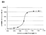
図3は、本発明の一実施形態に係るエピタキシャル成長工程のプロセス温度と、ウェーハの表面上のLPD個数との関係を示す図であり、エピタキシャル成長工程のプロセス温度(エピタキシャル成長実温度)を変えて実験した場合における、エピタキシャル成長工程のプロセス温度と、SFに起因してウェーハ表面に出現するLPDの個数との関係を示している。横軸は、エピタキシャル成長工程のプロセス温度を示し、縦軸は、ウェーハ1枚当りのウェーハ表面のLPD個数を示している。
FIG. 3 is a diagram showing the relationship between the process temperature of the epitaxial growth step according to an embodiment of the present invention and the number of LPDs on the surface of the wafer. The experiment was performed by changing the process temperature (epitaxial growth actual temperature) of the epitaxial growth step. 3 shows the relationship between the process temperature of the epitaxial growth step and the number of LPDs that appear on the wafer surface due to SF. The horizontal axis indicates the process temperature of the epitaxial growth step, and the vertical axis indicates the number of LPDs on the wafer surface per wafer.
ここで、縦軸に示されたウェーハ1枚当りのLPD個数は、KLA-Tencor社製SP-1のDCNモードで測定し、0.13μmサイズ以上であるLPDを検出して計数した結果の個数を示している。
Here, the number of LPDs per wafer indicated on the vertical axis is the number of results obtained by detecting and counting LPDs having a size of 0.13 μm or more, measured in the DCN mode of SP-1 manufactured by KLA-Tencor. Is shown.
また、本実験では、シリコン結晶育成時に上述した濃度範囲でリンとゲルマニウムが一緒にドープされた直径200mmのシリコン結晶基板を用いた。プロセス温度毎に25枚のシリコン結晶基板上にシリコンエピタキシャル層の形成を行った。図3に示される各プロセス温度でのLPD個数は、それらの25枚のウェーハのLPD個数の平均値である。
Also, in this experiment, a silicon crystal substrate having a diameter of 200 mm in which phosphorus and germanium are doped together in the above-described concentration range at the time of silicon crystal growth was used. A silicon epitaxial layer was formed on 25 silicon crystal substrates for each process temperature. The number of LPDs at each process temperature shown in FIG. 3 is an average value of the number of LPDs of those 25 wafers.
図3から分かるように、プロセス温度の範囲は、1110℃以上の範囲と、1110~1090℃の範囲と、1090℃以下(但し、1000℃以上)の範囲に大別できる。1110℃以上の範囲では、LPD個数は一万個以上と非常に多い。プロセス温度を下げていくと、1110~1090℃の範囲でLPD個数は急激に低下する。1100℃~1090℃の範囲では、LPD個数は多めに見ても略100個以下(ウェーハ表面の面積100cm2当たり32個以下)と少ない。更に、1090℃以下(但し、1000℃以上)の範囲では、LPD個数は多めに見ても30個以下(ウェーハ表面の面積100cm2当たり10個以下)と非常に少ない。従って、エピタキシャル成長時のプロセス温度は、1100℃以下が好ましく、1000℃~1090℃の範囲内がより好ましい。特に、1050℃~1080℃の範囲は、LPD個数が数個以下(ウェーハの表面の面積100cm2当たり2~0個程度)と極めて少なく、かつ、プロセス温度が1000℃以下の場合における上記の問題も少ないので、最適なプロセス温度範囲といえる。
As can be seen from FIG. 3, the process temperature range can be broadly divided into a range of 1110 ° C. or higher, a range of 1110 to 1090 ° C., and a range of 1090 ° C. or lower (however, 1000 ° C. or higher). In the range of 1110 ° C. or higher, the number of LPDs is as large as 10,000 or more. As the process temperature is lowered, the number of LPDs rapidly decreases in the range of 1110 to 1090 ° C. In the range of 1100 ° C. to 1090 ° C., the number of LPDs is as small as about 100 or less (32 or less per 100 cm 2 of the wafer surface area) even if it is a large number. Furthermore, in the range of 1090 ° C. or less (however, 1000 ° C. or more), the number of LPDs is very small, 30 or less (10 or less per 100 cm 2 of the wafer surface area) even if it is a large number. Accordingly, the process temperature during epitaxial growth is preferably 1100 ° C. or less, and more preferably in the range of 1000 ° C. to 1090 ° C. In particular, in the range of 1050 ° C. to 1080 ° C., the above problems occur when the number of LPDs is very few (about 2 to 0 per 100 cm 2 of the wafer surface area) and the process temperature is 1000 ° C. or less. Therefore, it can be said to be the optimum process temperature range.
以上、本発明の好適な実施形態を説明したが、これは本発明の説明のための例示であり、本発明の範囲をこの実施形態にのみ限定する趣旨ではない。本発明は、その要旨を逸脱しない範囲で、上記実施形態とは異なる種々の態様で実施することができる。
The preferred embodiment of the present invention has been described above. However, this is an example for explaining the present invention, and the scope of the present invention is not limited to this embodiment. The present invention can be implemented in various modes different from the above-described embodiments without departing from the gist thereof.