WO2010150693A1 - 光配向した液晶性ポリイミドによる位相差膜及び光学素子 - Google Patents
光配向した液晶性ポリイミドによる位相差膜及び光学素子 Download PDFInfo
- Publication number
- WO2010150693A1 WO2010150693A1 PCT/JP2010/060263 JP2010060263W WO2010150693A1 WO 2010150693 A1 WO2010150693 A1 WO 2010150693A1 JP 2010060263 W JP2010060263 W JP 2010060263W WO 2010150693 A1 WO2010150693 A1 WO 2010150693A1
- Authority
- WO
- WIPO (PCT)
- Prior art keywords
- retardation film
- film
- liquid crystal
- retardation
- light
- Prior art date
Links
Images


Classifications
-
- G—PHYSICS
- G02—OPTICS
- G02B—OPTICAL ELEMENTS, SYSTEMS OR APPARATUS
- G02B5/00—Optical elements other than lenses
- G02B5/30—Polarising elements
- G02B5/3083—Birefringent or phase retarding elements
-
- G—PHYSICS
- G02—OPTICS
- G02F—OPTICAL DEVICES OR ARRANGEMENTS FOR THE CONTROL OF LIGHT BY MODIFICATION OF THE OPTICAL PROPERTIES OF THE MEDIA OF THE ELEMENTS INVOLVED THEREIN; NON-LINEAR OPTICS; FREQUENCY-CHANGING OF LIGHT; OPTICAL LOGIC ELEMENTS; OPTICAL ANALOGUE/DIGITAL CONVERTERS
- G02F1/00—Devices or arrangements for the control of the intensity, colour, phase, polarisation or direction of light arriving from an independent light source, e.g. switching, gating or modulating; Non-linear optics
- G02F1/01—Devices or arrangements for the control of the intensity, colour, phase, polarisation or direction of light arriving from an independent light source, e.g. switching, gating or modulating; Non-linear optics for the control of the intensity, phase, polarisation or colour
- G02F1/13—Devices or arrangements for the control of the intensity, colour, phase, polarisation or direction of light arriving from an independent light source, e.g. switching, gating or modulating; Non-linear optics for the control of the intensity, phase, polarisation or colour based on liquid crystals, e.g. single liquid crystal display cells
- G02F1/133—Constructional arrangements; Operation of liquid crystal cells; Circuit arrangements
- G02F1/1333—Constructional arrangements; Manufacturing methods
- G02F1/1335—Structural association of cells with optical devices, e.g. polarisers or reflectors
- G02F1/13363—Birefringent elements, e.g. for optical compensation
Definitions
- the present invention relates to a retardation film produced by using a liquid crystalline polyimide having a photoreactive group, in which a plurality of regions having different optical characteristics of optical axis and retardation are patterned, an optical element having the retardation film, and a liquid crystal
- the present invention relates to a display device.
- the retardation film has a function of converting the polarization state before passing through the retardation film into another different polarization state depending on optical properties such as the size of the retardation and the axial angle of the optical axis. And other optical elements such as pickup optical systems and anti-counterfeiting.
- patterned retardation film patterning by changing optical characteristics such as the size of retardation and the axial angle of the optical axis for each predetermined region (hereinafter also referred to as “patterned retardation film”) is possible.
- the previous optical element is considered to improve the performance and also to create a unique optical element.
- a composition containing a liquid crystal compound to which a polymerizable functional group is added in order to fix the alignment hereinafter referred to as “Polmeric liquid crystal material ”
- a film hereinafter referred to as" photo-alignment film ” that is given an alignment regulating force for aligning liquid crystal molecules in a specific direction when irradiated with light such as polarized ultraviolet rays.
- Patent Document 1 by applying a polymerizable liquid crystal material on a photo-alignment film irradiated with polarized ultraviolet rays in a specific direction in a predetermined region, aligning the orientation, and curing the material, an optical axis is obtained.
- a retardation film in which different regions are patterned can be obtained.
- this technique requires a different technique for patterning related to retardation, which is an optical characteristic different from that of the optical axis.
- a method for obtaining a retardation film patterned by changing the retardation a method using a polymerizable liquid crystal material containing a photoisomerizable compound is known (for example, see Patent Document 2). .
- a photoisomerizable compound contained in a polymerizable liquid crystal material is photoisomerized from a trans isomer to a cis isomer by light irradiation, and the ratio of cis isomer / trans isomer increases as the amount of light irradiation increases.
- the ratio of the cis isomer / trans isomer of the photoisomerizable compound increases as the amount of light irradiation increases.
- the birefringence decreases. Therefore, by changing the light irradiation for each predetermined region, a retardation film in which regions having different retardation sizes are patterned can be obtained.
- this technique also requires another technique for patterning the optical axis, which is an optical characteristic different from retardation.
- a retardation film is used in a liquid crystal display device.
- Specific examples and problems to be solved are listed below.
- the so-called 1 / 4 ⁇ plate is used in a reflective liquid crystal display device or a transflective liquid crystal display device.
- the quarter ⁇ plate is a retardation film having a retardation that is 1 ⁇ 4 of the wavelength ⁇ with respect to a specific wavelength ⁇ .
- the retardation in typical wavelength lambda m is a phase difference film which is adjusted to 1/4 the size of the wavelength lambda m is used, at a wavelength other than lambda m since the retardation is different from the ideal size In a liquid crystal display device on which it is mounted, a sufficiently satisfactory value cannot be obtained in characteristics relating to the performance of the display device such as a contrast ratio.
- a wavelength band corresponding to each color filter layer is used.
- typical wavelengths ⁇ 1, ⁇ 2, ⁇ , ⁇ retardation for m is ⁇ 1/4, ⁇ 2/ 4, the ⁇ ⁇ ⁇ lambda m / 4 size has been a phase difference film, adjusted to It is effective to form a pattern corresponding to color filter layers having different spectral transmittance characteristics in the color filter.
- the patterned retardation film is formed in the color filter layer and arranged inside the liquid crystal panel in consideration of the influence of parallax.
- the patterned retardation film is also required to have heat resistance such that the characteristics of the retardation film do not change beyond the allowable range with respect to the processing temperature and thermal history of these film forming processes.
- the present invention provides a technique capable of manufacturing a retardation film patterned with a region with different optical characteristics of one or both of the optical axis and retardation with less load.
- the present invention further provides an optical element and a liquid crystal display element using the patterned retardation film.
- the present inventors develop a thermotropic liquid crystal property by heating and imidization, and also have a specific structure of the polyamic acid having photo-alignment property, photo-align the polyamic acid in the coating film, It has been found that the thin film obtained by imidization can also be used as a retardation film due to the large optical anisotropy obtained by the liquid crystallinity expressed by the imidization, and further, photoalignment is performed in the coating film.
- optical properties such as the optical axis angle and retardation size of the thin film can be controlled by irradiating light while controlling the polarization state and irradiation energy intensity of the thin film, and completed the present invention. I let you.
- the present invention provides a retardation film made of a material containing polyimide having a photoreactive group and exhibiting liquid crystallinity.
- the present invention also provides the above-mentioned retardation film in which a pattern comprising at least two or more regions in which one or both of the direction of the optical axis and the retardation are different is formed.
- the present invention also provides the retardation film obtained by irradiating light having different polarization states.
- the present invention also provides the retardation film obtained by irradiating light having an arbitrary polarization state with different illuminance or irradiation energy intensity.
- the present invention also provides the retardation film obtained by forming different film thicknesses.
- the present invention also includes (1) irradiation with light of different polarization states, (2) irradiation of light having an arbitrary polarization state with different illuminance or irradiation energy intensity, and (3) formation of different film thicknesses.
- the retardation film obtained by combining at least two techniques is provided.
- the present invention is a polyimide film in which the liquid crystalline polyimide film has a photoreactive group and exhibits optical anisotropy by light irradiation and baking of a polyamic acid that exhibits liquid crystallinity by imidization.
- the retardation film is provided.
- the present invention also provides an optical element having the retardation film of the present invention.
- the present invention also provides a patterned retardation film in which a pattern composed of at least two or more regions in which one or both of the direction of the optical axis and the size of the retardation are different, and the direction of the optical axis and the size of the retardation.
- the optical element is provided with a uniform non-patterned retardation film, and the patterned retardation film is the retardation film of the present invention.
- the present invention also provides the above optical element, wherein at least one layer of the non-patterned retardation film is a film in which the alignment state of the liquid crystal compound is fixed by crosslinking or polymerization of the liquid crystal compound having a polymerizable functional group. .
- the present invention also provides the optical element in which an unpatterned retardation film in which an alignment state of a liquid crystal compound is fixed by crosslinking or polymerization is directly formed on the patterned retardation film.
- the patterned retardation film is a patterned retardation film whose surface is rubbed or whose surface is irradiated with ultraviolet rays.
- the alignment state of the liquid crystal compound is crosslinked or polymerized.
- the above-described optical element in which a fixed non-patterned retardation film is formed.
- the present invention also provides the optical element, wherein the alignment state of the liquid crystal compound is horizontal alignment.
- the present invention also provides the optical element, wherein the alignment state of the liquid crystal compound is splay alignment or hybrid alignment.
- the present invention also provides the optical element, wherein the alignment state of the liquid crystal compound is vertical alignment.
- the present invention also provides the optical element, wherein the alignment state of the liquid crystal compound is a spirally twisted alignment.
- the present invention also provides the above-described optical element which is an anti-counterfeit element.
- the present invention also provides a display device having the retardation film of the present invention.
- the present invention also provides a liquid crystal display device having the retardation film of the present invention.
- the present invention further includes a color filter that selectively transmits light in a specific wavelength range, and the color filter selectively and independently transmits light in two or more specific wavelength ranges for each pixel.
- a color filter that selectively transmits light in a specific wavelength range
- the color filter selectively and independently transmits light in two or more specific wavelength ranges for each pixel.
- the liquid crystal display device having a color filter layer to be transmitted and a retardation film provided corresponding to the color filter layer, wherein the retardation film is the retardation film of the present invention.
- the retardation film is different in one or both of the direction of the optical axis and the size of the retardation corresponding to each region of the color filter layer that selectively transmits light in a specific wavelength range.
- the liquid crystal display device is a retardation film in which a pattern composed of two or more regions is formed.
- the retardation film is provided as a region where the reflection plate is provided.
- the liquid crystal display device is a retardation film in which a pattern including two or more regions in which one or both of the direction of the optical axis and the magnitude of the retardation are different from each other is formed.
- the present invention is the color filter in which the color filter is formed with a pattern composed of two or more regions of a color filter layer that selectively transmits light in a specific wavelength region, and the retardation film is a spectral filter.
- the retardation film is a retardation film in which a pattern comprising two or more regions in which one or both of the direction of the optical axis and the size of the retardation are different from each other further corresponds to each region of the color filter layer having different transmittance characteristics.
- a liquid crystal display device is provided.
- the optical characteristics that is, the direction of the optical axis (axis angle) and the size of the retardation are adjusted by the polarization state of the light irradiated to the polyamic acid film before heating and imidization, the irradiation energy intensity, and the like.
- a retardation film having high heat resistance unique to polyimide can be obtained. Therefore, the present invention can provide a technique capable of manufacturing a retardation film in which regions having different one or both of the optical axis angle and retardation size are patterned with a smaller number of members and processes.
- the present invention can also provide an optical element and a liquid crystal display element using the patterned retardation film with a smaller number of members and processes.
- FIG. 3 is a diagram showing a relationship between irradiation energy intensity and birefringence in the retardation film of Example 1. It is a figure which shows the spectral transmittance characteristic of the comparative example 1 of Example 5, and the example 2 of an invention. It is a figure which shows the spectral transmittance characteristic of the comparative example 3 of Example 6, and the example 6 of an invention.
- the retardation film of the present invention is made of a material including a polyimide having a photoreactive group and exhibiting liquid crystallinity (hereinafter also referred to as “liquid crystalline polyimide”).
- the liquid crystalline polyimide is a general term for polyimides having a photoreactive group in the main chain or side chain of the liquid crystalline polyimide and exhibiting liquid crystallinity such as thermotropic liquid crystallinity or lyotropic liquid crystallinity.
- liquid crystallinity such as thermotropic liquid crystallinity or lyotropic liquid crystallinity.
- the average molecular weight of the liquid crystalline polyimide is not particularly limited, but it prevents the evaporation of the liquid crystalline polyimide during baking of the coating film, and from the viewpoint of the expression of preferable physical properties in the material, the weight average molecular weight is 5 ⁇ 10 3 or more. Preferably, it is 1 ⁇ 10 4 or more. The weight average molecular weight is preferably 1 ⁇ 10 6 or less from the viewpoint of easy handling of the material such as viscosity.
- the weight average molecular weight of the liquid crystalline polyimide is measured by a gel permeation chromatography (GPC) method.
- GPC gel permeation chromatography
- a liquid crystalline polyimide or its precursor polyamic acid is diluted with dimethylformamide (DMF) so that the concentration of the liquid crystalline polyimide or its precursor is about 1% by weight, for example, Chromatopack C-R7A (Shimadzu) It is calculated
- DMF dimethylformamide
- a developing solvent in which an inorganic acid such as phosphoric acid, hydrochloric acid, nitric acid, sulfuric acid or the like or an inorganic salt such as lithium bromide or lithium chloride is dissolved in a DMF solvent may be prepared and used.
- the photoreactive group is a group that orients a specific molecular structure such as a mesogenic group in liquid crystalline polyimide in one direction by irradiation with specific light.
- One or more photoreactive groups may be used.
- azobenzene is known to undergo a photoisomerization reaction that changes to a trans form having the major axis of the molecular structure of azobenzene in a direction perpendicular to the polarization direction when irradiated with linearly polarized light in the wavelength range of 300 to 400 nm.
- As the photoreactive group a group that changes to a specific structure by photoisomerization reaction or photocrosslinking reaction when irradiated with specific light can be used.
- Examples of the photoreactive group that undergoes photoisomerization reaction include an azo group that includes a double bond between nitrogen atoms, a vinylene group that includes a double bond between carbon atoms, and a triple bond between carbon atoms.
- An ethynyl group which is a group containing Examples of the photoreactive group that undergoes a photocrosslinking reaction include a group having a cinnamic acid structure, a group having a coumaric acid structure, and a group having chalcone acid.
- the photoreactive group is preferably a photoreactive group that undergoes a photoisomerization reaction.
- the content of the photoreactive group in the liquid crystalline polyimide is selected from the viewpoint of expressing the desired optical anisotropy in the retardation film of the present invention, for example, the viewpoint of aligning the mesogenic group in a predetermined direction according to the irradiated light. Therefore, it is preferably contained in an amount of 10 to 50 mol% with respect to the imide group in the liquid crystalline polyimide.
- the liquid crystalline polyimide is composed of the photoreactive group, a mesogenic group having a rigid molecular structure, and a spacer group having a flexible molecular structure.
- a main chain type liquid crystalline polyimide can be formed by forming a main chain including a photoreactive group, a mesogen group, and a spacer group, and a side chain including a photoreactive group, a mesogen group, and a spacer group is formed. By doing so, a side chain type liquid crystalline polyimide can be constituted.
- a known structure can be adopted for the mesogenic group and the spacer group.
- Examples of the mesogenic group include groups containing an aromatic imide ring, azobenzene, biphenyl, phenylbenzoate, azoxybenzene, stilbene, terphenyl and the like.
- Examples of the spacer group include linear alkyl groups having about 1 to 20 carbon atoms.
- the retardation film of the present invention forms a coating film of a solution of liquid crystalline polyimide or a precursor thereof, irradiates the formed coating film with specific light, and reacts with a photoreactive group to react with the liquid crystalline polyimide or a precursor thereof. It can be obtained by orienting the body and firing the photo-oriented film.
- the liquid crystalline polyimide or precursor thereof may be a compound that is photo-aligned by irradiation with specific light in the coating film.
- the liquid crystalline polyimide is a polyimide that exhibits liquid crystallinity at least during the phase difference film formation after photo-alignment.
- the liquid crystalline polyimide may be a polyimide that exhibits liquid crystallinity in a solution or a coating film, and may be heated during baking, that is, at a certain temperature or higher. Polyimide exhibiting liquid crystallinity may be used in the obtained film.
- the liquid crystalline polyimide include a polyimide having a photoreactive group and a mesogenic structure and dissolved in a solvent described later at a concentration of 1% by weight or more.
- Examples of the precursor of the liquid crystalline polyimide include polyamic acid having a photoreactive group and a mesogenic structure.
- concentration of the said liquid crystalline polyimide can be determined according to the use of the retardation film of this invention.
- the thickness of the retardation film is about 30 nm from the birefringence of the material.
- the liquid crystalline polyimide The lower limit of the concentration of can be set to 1% by weight.
- the angle of the optical axis and the size of retardation in the retardation film can be adjusted.
- a retardation film having an optical axis parallel to the polarization direction of irradiated light can be obtained by irradiating linearly polarized light perpendicularly to the coating film.
- a retardation film having an optical axis parallel to the major axis direction of elliptically polarized light can be obtained by irradiating elliptically polarized light perpendicularly to the coating film.
- a retardation film (polyimide film) in which the direction of the optical axis is not specified can be obtained by irradiating non-polarized light perpendicularly to the coating film.
- the magnitude of the birefringence ⁇ n of the retardation film can be adjusted in proportion to the intensity of light irradiation energy to the coating film, and the retardation Re of the retardation film can be adjusted. can do. That is, the ⁇ n and Re can be increased by increasing the light irradiation energy intensity to the coating film, and the ⁇ n and Re can be decreased by decreasing the light irradiation energy intensity to the coating film. be able to.
- the magnitude of Re can be adjusted in proportion to the thickness of the retardation film. That is, the Re can be increased by increasing the thickness of the retardation film, and the Re can be decreased by decreasing the thickness of the retardation film.
- the film thickness of the retardation film can be adjusted by, for example, the viscosity or concentration of the liquid crystalline polyimide solution or its precursor solution, or the number of coatings, and can be increased by increasing at least one of these.
- Re and ⁇ n can be adjusted by using two or more kinds of the liquid crystalline polyimides in combination.
- the light applied to the coating film for photo-alignment may be light that causes a reaction that changes the orientation of the liquid crystalline polyimide to the photoreactive group described above.
- Examples of such light include light (ultraviolet light) having a wavelength of 300 to 400 nm.
- the irradiation energy intensity of the irradiation light is preferably less than 10 J / cm 2 from the viewpoint of giving an appropriate orientation to the polyamic acid, for example.
- the retardation film of the present invention can adjust the optical characteristics by light irradiation, it can be controlled within the same film by controlling the polarization state and irradiation energy intensity of the irradiated light together with a masking technique such as a photomask. In this case, a plurality of regions having different optical characteristics can be formed easily and precisely.
- the retardation film of the present invention can align the liquid crystal compound along the direction of the optical axis of the liquid crystalline polyimide when the liquid crystal layer is formed on the retardation film. Furthermore, when the liquid crystal layer is formed on the retardation film after the surface of the retardation film is rubbed, the liquid crystal compound is aligned along the rubbing direction regardless of the direction of the optical axis of the liquid crystalline polyimide. Can be made.
- the retardation film of the present invention has a liquid crystal compound in the liquid crystal layer as described in JP-A-2009-69493.
- the pretilt angle of the liquid crystal compound can be adjusted by mixing a polyamic acid having a diamine having a specific structure (side chain structure) that imparts a pretilt angle of 2 with a liquid crystal polyimide precursor solution.
- the pretilt angle can be lowered by irradiating the coating film of the solution with specific polarized ultraviolet light (for example, polarized ultraviolet light having a short wavelength of 300 nm or less).
- the retardation film of the present invention is adjusted in the same manner as a known retardation film by adjusting its optical characteristics to appropriate characteristics according to the use of the retardation film by the various methods described above.
- the functional polyimide has a uniaxial property and can be used in various applications such as an A plate having an optical axis in the film plane, a 1 / 4 ⁇ plate, a 1 / 2 ⁇ plate, an optical compensation film, and a polarization rotator.
- the retardation film of the present invention is a polyimide film, it has high heat resistance, and has stable optical characteristics with little change even after a thermal load exceeding 200 ° C. is applied. Therefore, in an optical element in which another layer such as one or more films is formed on the retardation film, an optical element manufacturing environment in which the firing step performed to form those layers is repeatedly performed. And can be widely applied to optical elements such as liquid crystal display elements.
- the optical characteristics that is, the direction of the optical axis and the size of the retardation are obtained by a manufacturing method with a smaller number of members and the number of steps as compared with a conventional manufacturing method of a retardation film using an alignment film and a liquid crystalline material.
- a plurality of regions different from each other can be formed in the same plane of the retardation film.
- a preferred example is a composition containing at least one polymer selected from a polyamic acid having a photoreactive group in the main chain and a polyimide obtained by a dehydration reaction thereof, between 100 ° C. and 300 ° C.
- the liquid crystal has a temperature range.
- Table 1 shows the diamine and acid anhydride compounds constituting the polyamic acid that can provide such characteristics, and Table 2 shows examples of the combinations.
- R 1 represents alkylene having 6 to 20 carbon atoms. A preferred carbon number is 6-12.
- R 2 represents one or two non-adjacent —CH 2 — is —O—, —NH—, —N (CH 3 ) —, —Si ( CH 3 ) 2 OSi (CH 3 ) 2 — or —COO— represents alkylene having 6 to 20 carbon atoms which may be replaced by —COO—.
- R 3 is one or two non-adjacent —CH 2 — is —O—, —NH—, —N (CH 3 ) —, —Si (CH 3 ) represents an alkylene having 6 to 20 carbon atoms which may be replaced by 2 OSi (CH 3 ) 2 — or —COO—.
- liquid crystalline polyimide having a photoreactive group of the present invention examples include a material containing a polyimide obtained by dehydrating a polyamic acid selected from the above-mentioned four preferable polyamic acids. Two or more polyamic acids may be selected.
- diamines other than the diamines mentioned in the above explanation, or acid anhydrides other than the acid anhydrides mentioned in the above explanation can be used in combination.
- diamines described in paragraphs 0077 to 0098 of JP-A-2009-69493 examples include the diamines described in paragraphs 0077 to 0098 of JP-A-2009-69493.
- acid anhydrides that can be used in combination include acid anhydrides described in paragraphs 0103 to 0125 of JP2009-69493A.
- examples of acid anhydrides that can be used in combination include compounds and formulas (IX-1) to (IX-4).
- a polyamic acid containing a structure of such an acid anhydride is preferable from the viewpoint of improving the solubility in a solvent even in a polyimide obtained by imidizing the polyamic acid.
- R 7 represents hydrogen or a methyl group.
- the polyamic acid can take various compositions from the viewpoint of desired properties when utilizing the two functions of the retardation film or the retardation film and the alignment film.
- the polyamic acid may be a copolymer composed of a diamine having a photoreactive group and a diamine having no photoreactive group, and the acid anhydride has a photoreactive group.
- the copolymer which consists of an acid anhydride and an acid anhydride which does not have a photoreactive group may be sufficient.
- the polyamic acid a mixture of a polyamic acid having two or more kinds of photoreactive groups or a mixture of a polyamic acid having a photoreactive group and a polyamic acid having no photoreactive group may be used. it can.
- the content of the photoreactive group in the polyamic acid is based on the assumption that the polyamic acid is 100% imidized from the viewpoint of orienting the mesogenic group in a predetermined direction according to the polarized light to be irradiated. More preferably, it is 10 to 50 mol%.
- the material for forming the coating film containing liquid crystalline polyimide or a precursor thereof is a material other than liquid crystalline polyimide or a precursor thereof (in the range in which liquid crystal properties of liquid crystalline polyimide are obtained) , Also referred to as “additive”).
- additive One type or two or more types of additives may be used.
- the polyamic polyimide is within a range in which the liquid crystalline polyimide has a characteristic having a liquid crystal temperature range between 100 ° C. and 300 ° C.
- Additives can be incorporated into the material up to less than 50 parts by weight with respect to 100 parts by weight of acid.
- the material may contain a polyamic acid containing no photoreactive group.
- examples of such polyamic acid include linear polyamic acid and polyamic acid having a side chain structure. These polyamic acids, for example, improve the electrical characteristics and orientation characteristics of the film or improve the orientation characteristics of the liquid crystal when using the obtained retardation film as a driving liquid crystal medium or an orientation film of a liquid crystalline material. It can be added from the viewpoint of changing.
- the material may contain a non-polyimide liquid crystal polymer from the viewpoint of improving liquid crystallinity.
- liquid crystal polymers include Handbook of Liquid Crystals Vol. 3 (published by WILEY-VCH published in 1998), main chain type thermotropic liquid crystal polymer, side chain type thermotropic liquid crystal polymer, and the like.
- the material may contain a liquid crystalline compound having a polymerizable functional group from the viewpoint of improving liquid crystallinity. Specific examples of such polymerizable liquid crystal compounds are illustrated below.
- P represents a polymerizable functional group.
- R 4 is independently —F, —Cl, —CN, —NO 2 , —OH, —OCH 3 , —OCN, —SCN, —OCF 3 , or halogen having 1 to 12 carbon atoms.
- Alkyl having 1 to 12 carbon atoms, alkyl having 1 to 12 carbon atoms, alkoxycarbonyl having 1 to 12 carbon atoms, alkylcarbonyloxy having 1 to 12 carbon atoms, or alkoxy having 1 to 12 carbon atoms Represents 1 to 12 alkoxycarbonyloxy.
- R 5 and R 6 are each —H, —F, —Cl, —CN, alkyl having 1 to 7 carbon atoms which may be halogenated, or alkoxy having 1 to 7 carbon atoms.
- A represents 1,4-phenylene or 1,4-cyclohexylene which may be mono-substituted, di-substituted or tri-substituted by R 5 .
- u represents 0 or 1
- v represents 0, 1 or 2
- x and y independently represent 1 to 12.
- Preferred examples of the polymerizable functional group include the following structures.
- W 1 represents —H or alkyl having 1 to 5 carbon atoms
- n represents 0 or 1.
- Crosslinking agent a compound having two or more functional groups that react with a carboxylic acid residue of a polyamic acid, a so-called cross-linking agent, is added to the material from the viewpoint of preventing deterioration with time and deterioration due to the environment. Further, it may be contained.
- a crosslinking agent include polyfunctional epoxies and isocyanate materials as described in Japanese Patent No. 3049699, Japanese Patent Application Laid-Open No. 2005-275360, Japanese Patent Application Laid-Open No. 10-212484, and the like.
- a crosslinking agent that reacts with the crosslinking agent itself to form a network polymer and improves the film strength of polyamic acid or polyimide can be used for the same purpose as described above.
- examples of such a crosslinking agent include polyfunctional vinyl ethers, maleimides, and bisallyl nadiimide derivatives as described in, for example, JP-A-10-310608, JP-A-2004-341030.
- the preferable content of these crosslinking agents is less than 50 parts by weight, more preferably less than 30 parts by weight, based on 100 parts by weight of the polyamic acid which is a precursor of liquid crystalline polyimide.
- the material may further contain an organosilicon compound from the viewpoint of adjusting the adhesion to the glass substrate.
- organosilicon compound include aminopropyltrimethoxysilane, aminopropyltriethoxysilane, vinyltrimethoxysilane, N- (2-aminoethyl) -3-aminopropylmethyldimethoxysilane, and N- (2-aminoethyl).
- the addition amount of the organosilicon compound is preferably 0.01 to 5 parts by weight, and more preferably 0.1 to 3 parts by weight with respect to 100 parts by weight of the liquid crystalline polyimide or precursor thereof.
- the material may further contain various additives as desired.
- the material contains a surfactant in accordance with the purpose when further improvement of coating properties is desired, an antistatic agent when desired to further improve antistatic properties, and a polymerizable liquid crystal compound or a crosslinking agent.
- a polymerizable liquid crystal compound or a crosslinking agent In order to promote the polymerization reaction or the crosslinking reaction, an appropriate amount of a polymerization initiator may be contained.
- the material containing the liquid crystalline polyimide or a precursor thereof and the above-described additive is referred to as a retardation film material.
- the phase difference film material can be used in a form dissolved in a solvent having the ability to dissolve it.
- a solvent having the ability to dissolve it is referred to as a retardation film material solution.
- Such solvents widely include solvents usually used in the production and use of polyamic acid or derivatives thereof, and can be appropriately selected according to the purpose of use. Examples of these solvents are as follows.
- aprotic polar organic solvents examples include N-methyl-2-pyrrolidone (NMP), dimethylimidazolidinone, N-methylcaprolactam, N-methylpropionamide, N, N—
- lactones such as dimethylacetamide, dimethylsulfoxide, N, N-dimethylformamide (DMF), N, N-diethylformamide, N, N-diethylacetamide (DMAc), and ⁇ -butyrolactone (GBL).
- solvents other than the above-mentioned solvents for the purpose of improving coatability include alkyl lactate, 3-methyl-3-methoxybutanol, tetralin, isophorone, ethylene glycol monobutyl ether (BCS), etc.
- Dipropylene glycol monoalkyl ethers such as dialkyl malonate and dipropylene glycol monomethyl ether, and these glycol monoethers Ester compounds such as Le acids and the like.
- NMP, dimethylimidazolidinone, GBL, BCS, diethylene glycol monoethyl ether, propylene glycol monobutyl ether, dipropylene glycol monomethyl ether and the like can be particularly preferably used as the solvent.
- the solvent may be contained so that the solid content in the retardation film material solution has an appropriate value according to the following various coating methods.
- the content of the solvent in the retardation film material solution is usually 0.1 to 30% by weight of the solid content in the retardation film material solution from the viewpoint of suppressing unevenness and pinholes during coating.
- the amount is preferably 1 to 20% by weight.
- the retardation film of the present invention is obtained by irradiating a coating film obtained by applying the above-described retardation film material solution onto a substrate with light having an arbitrary polarization state, and photoreactivity of a polyamic acid having a photoreactive group. Anisotropy is imparted to the orientation of the group, and then heated to the liquid crystal temperature range of the coating film to form (baking) a liquid crystalline polyimide film by dehydration of the polyamic acid, and the optical anisotropy of the formed film It is obtained by expressing and increasing sex.
- the retardation film of the present invention is preferably produced by the following procedure.
- the retardation film material solution is applied onto a substrate by a brush coating method, a dipping method, a spinner method, a spray method, a printing method, an ink jet method or the like.
- the coating film formed on the substrate is heated at 50 to 120 ° C., preferably 80 to 100 ° C., to evaporate the solvent.
- the coating film is irradiated with light having an arbitrary polarization state to orient the polyamic acid in the coating film.
- the coating film in which the polyamic acid is oriented is heated at 150 to 300 ° C., preferably 180 to 250 ° C. to imidize, and a liquid crystal phase is developed.
- linearly polarized light is preferably used for the orientation of the polyamic acid.
- the photoreactive group is azobenzene
- the major axis of the molecular structure of azobenzene is oriented in a direction perpendicular to the polarization direction by irradiation with linearly polarized light.
- the linearly polarized light is not particularly limited as long as it is light capable of orienting the polyamic acid in the coating film.
- the polyamic acid can be oriented by low energy light irradiation.
- the irradiation amount of linearly polarized light in the photo-alignment treatment of the polyamic acid is preferably less than 10 J / cm 2 .
- the wavelength of linearly polarized light is preferably 300 to 400 nm.
- a conventional photo-alignment film using an aligning agent has a function as an alignment film for aligning a liquid crystal material such as a polymerizable liquid crystal material, but is sufficient as a retardation film in properties such as retardation. It's hard to be done.
- a liquid crystalline polyimide containing a photoreactive group by aligning itself, has sufficient characteristics as a retardation film in addition to the function as an alignment film, in the same manner as a conventional photo-alignment film. Is different from the conventional aligning agent.
- the arbitrary polarization state is a specific polarization state selected from linear polarization, circular polarization, elliptical polarization, and non-polarization.
- the direction of the optical axis and the size of retardation in the retardation film are controlled.
- the polyamic acid film Prior to heating imidization, the polyamic acid film is irradiated with light of different polarization states several times together with a masking technique such as a photomask, and then heated to a temperature at which imidization and liquid crystal phase are manifested at once.
- a patterned retardation film in which the direction of the optical axis and the size of the retardation are different for each predetermined region can be obtained.
- the retardation of the retardation film is controlled by irradiating light of an arbitrary polarization state on the polyamic acid coating film with different illuminance or irradiation energy intensity.
- the film of polyamic acid is irradiated with light of any polarization state by changing the illuminance or irradiation energy intensity together with masking technology such as photomask, and then imidized at once, and the liquid crystal phase is changed By heating to the temperature at which it is developed, a patterned retardation film having different retardation sizes for each predetermined region can be obtained.
- a retardation film having a different film thickness is formed for each predetermined region.
- the size of retardation in the retardation film is controlled.
- the thickness of each coating film region can be selected by selectively applying a material solution for a retardation film (concentration, viscosity, composition, etc.) to a specific region in the same film, such as an inkjet method. It can be changed by forming the coating film in a way that can be done.
- the retardation film in which one or both optical characteristics of the optical axis and retardation in the present invention are patterned can be obtained by combining these methods independently and arbitrarily two or more.
- the optical element of the present invention has the retardation film of the present invention described above.
- the optical element in the present invention only needs to have at least one retardation film of the present invention described above, and may have a plurality of retardation films of the present invention, or a liquid crystal containing a photoreactive group.
- a retardation film formed from a material other than the liquid crystalline polyimide containing the photoreactive group may be included.
- the type of the retardation film of the present invention that the optical element of the present invention has is not particularly limited.
- the anisotropy of the refractive index of the retardation film will be described using an orthogonal coordinate system.
- the refractive index of the retardation film when the axes parallel to and perpendicular to the plane of the retardation film are x-axis and y-axis and the axis perpendicular to the surface of the retardation film is z-axis is Can be decomposed in a direction parallel to Resolved refractive indexes corresponding to the x, y, and z axes are nx, ny, and nz, respectively, and the thickness of the retardation film is d.
- the X axis and Y axis correspond to the axis of the XY plane, which is a plane parallel to the film plane of the retardation film or polarizing plate, and the axis parallel to the normal line of the film plane of the retardation film or polarizing plate is the Z axis.
- the retardation film is an A plate described later, its optical axis corresponds to the x axis when the A plate is a positive A plate, and corresponds to the y axis when the A plate is a negative A plate. As shown in FIG.
- the axis angle 1 of the optical axis is represented by an angle formed by the optical axis and the X axis, and increases positively counterclockwise. Is displayed. Further, when the retardation film is a C plate described later, the z-axis that is the optical axis is parallel to the Z-axis.
- the axis angle 2 of the absorption axis of the polarizing plate is represented by the angle formed by the absorption axis of the polarizing plate and the X axis, and is displayed so as to increase positively counterclockwise.
- a plane including the observer's observation direction (the direction of the line of sight) and the Z axis is referred to as an incident surface 3
- the angle formed by the incident surface 3 is referred to as an azimuth angle 4, and the angle formed by the observer's observation direction and the Z axis within the incident surface 3 is referred to as a polar angle 5.
- the azimuth angle 4 is displayed so as to increase positively counterclockwise with respect to the reference direction (for example, the direction of the optical axis of the retardation film).
- the polar angle 5 is displayed so as to increase positively from the Z axis.
- the retardation film is classified based on the difference in magnitude of nx, ny, and nz of each refractive index in the triaxial directions shown in FIG.
- nx> ny nz.
- It may be expressed as a retardation film that exhibits positive uniaxiality and whose optical axis is parallel to the thin film surface of the retardation film. It can be obtained by stretching a transparent resin having a positive intrinsic birefringence such as a cyclic olefin resin or a modified polycarbonate resin under specific conditions.
- a director of a liquid crystal material having a rod-like mesogen skeleton can be obtained by forming a uniform homogeneous orientation on a transparent substrate and fixing it.
- An example of horizontally aligning a polymerizable liquid crystal material having a rod-like mesogen skeleton is described in JP-A-2006-307150.
- a transparent resin having a positive intrinsic birefringence such as a cyclic olefin resin, a polycarbonate resin, a cellulose resin, an acrylic resin, a polyamideimide resin, a polyether ether ketone resin, and a polyimide resin is stretched under specific conditions.
- a thin film is formed by a solvent casting method, the film is obtained by spontaneously orienting molecules during the evaporation of the solvent.
- nx ny ⁇ nz.
- It may be expressed as a retardation film that exhibits positive uniaxiality and whose optical axis coincides with the normal direction of the thin film surface of the retardation film. It can be obtained by stretching a resin having a negative intrinsic birefringence such as a polystyrene-based resin and an N-substituted maleimide copolymer under specific conditions. Alternatively, it can also be obtained by forming and fixing a homeotropic alignment of a liquid crystalline material having a rod-like mesogenic skeleton on a transparent substrate. An example of homeotropic alignment of a polymerizable liquid crystal material having a rod-like mesogenic skeleton is described in JP-A No. 2006-188862.
- nz nx> ny. It may be expressed as a retardation film that exhibits negative uniaxiality and whose optical axis is parallel to the thin film surface of the retardation film. It can be obtained by stretching a transparent resin having a negative intrinsic birefringence, such as a polystyrene resin and an N-substituted maleimide copolymer, under specific conditions.
- the liquid crystal material director having a disk-like mesogen skeleton can be obtained by forming a uniform homogeneous orientation on a transparent substrate and fixing it. There is also a report that it can be obtained by the shape of the supramolecular packing by the discoid molecule or the rectangular molecule expressed in the lyotropic phase and the orientation form thereof.
- Biaxial plate (I) As a relationship of the refractive index in the triaxial direction, nx>ny> nz is satisfied.
- a resin having a positive intrinsic birefringence such as a cyclic olefin resin, a polycarbonate resin, a cellulose resin, an acrylic resin, a polyamideimide resin, a polyetheretherketone resin, and a polyimide resin under specific conditions. can get. Alternatively, it can also be obtained by further stretching a negative C plate obtained from the transparent resin described above.
- a liquid crystal material having a rod-like mesogen skeleton and having a helical orientation in which the helical pitch periodically changes in the direction of the helical axis More specifically, a polymerizable cholesteric liquid crystal material containing a dichroic polymerization initiator is used to form an orientation in which the helical axis is parallel to the normal direction of the transparent substrate surface and the helical pitch is less than 300 nm. It can be obtained by irradiating it with polarized ultraviolet rays.
- Free radicals are more likely to be generated as the direction of polarization of ultraviolet light and the director of the dichroic polymerization initiator are parallel, and this is thought to be due to the occurrence of a periodic concentration gradient in the generation of free radicals in the direction of the helical axis. It is described in JP-T-2005-513241.
- Biaxial plate (II) As a relationship of the refractive index in the triaxial direction, nx>nz> ny is satisfied. It can be obtained by stretching a cyclic olefin resin or the like under special conditions. It is described in JP-A-2006-72309. There is also a report that it is obtained by the shape of the supramolecular packing by the rectangular molecules expressed in the lyotropic phase and the orientation form thereof.
- Biaxial plate (III) As a relationship of refractive indexes in the triaxial direction, nz>nx> ny is satisfied. It can be obtained by stretching the above-mentioned transparent resin having a negative intrinsic birefringence under specific conditions.
- Retardation film obtained from tilted liquid crystal material In a film in which a liquid crystal material having a rod-like or disk-like mesogen skeleton is fixed on a transparent substrate, the director is between the substrate plane and horizontal to vertical. It is a phase difference film tilted at. When the tilt angle is constant from the substrate interface to the air interface, the orientation is referred to as splay orientation, and when the tilt angle changes continuously, the orientation is referred to as hybrid orientation.
- splay orientation When the tilt angle is constant from the substrate interface to the air interface, the orientation is referred to as splay orientation, and when the tilt angle changes continuously, the orientation is referred to as hybrid orientation.
- An example in which a polymerizable liquid crystal material having a rod-like mesogenic skeleton is tilted is described in JP-A-2006-307150 and the like.
- Retardation film (II) optical rotator obtained from helically aligned liquid crystalline material When the helical pitch is longer than the target wavelength, the function as an optical rotator is exhibited.
- An example of spirally aligning a polymerizable liquid crystal material having a rod-like mesogen skeleton is described in JP-A No. 2005-171235.
- such a type of retardation film can be produced according to various conditions such as the type of liquid crystalline polyimide or its precursor, the type of additive, and the polarization state and irradiation direction in light irradiation.
- the polyamic acid containing the above-mentioned photoreactive group is used to irradiate the coating film with linearly polarized light from the direction in which the light beam direction coincides with the normal direction of the thin film surface at 150 to 300 ° C.
- the positive A plate described above can be formed.
- Conventionally known retardation films may be used for the various retardation films described above, and the various retardation films described above can be installed at arbitrary positions in the optical element of the present invention.
- an optical element of the present invention having such a retardation film of the present invention and a conventional retardation film for example, there is a pattern comprising at least two or more regions in which one or both of the direction of the optical axis and the retardation are different.
- An optical element in which the retardation film is the above-described known retardation film is exemplified.
- the non-patterned retardation film can be arbitrarily used from the above-mentioned known retardation films, but can be thinned and does not require a stretching process for expressing optical anisotropy, Furthermore, from the viewpoint of optical element performance and production such as excellent heat resistance, it is a retardation film made of a polymerizable liquid crystal material in which the alignment state of the liquid crystal compound is fixed by crosslinking or polymerization of a liquid crystal compound having a polymerizable functional group. It is preferable.
- the liquid crystal compound may be one kind or two or more kinds.
- Such a non-patterned phase difference film may be a single layer or two or more layers of the non-patterned phase difference film in the optical element of the present invention. Examples of the polymerizable liquid crystal material include materials described in JP-A-2006-307150, JP-A-2005-263778, and the like.
- the polymerizable liquid crystal layer of the non-patterned retardation film can be a liquid crystal layer of various forms by employing an appropriate liquid crystal compound.
- Examples of the alignment state of the liquid crystal in such a liquid crystal layer include horizontal alignment, splay alignment or hybrid alignment, vertical alignment, and helically twisted alignment.
- the retardation film of the present invention and the non-patterned retardation film may be in direct contact with each other or may be disposed with another layer interposed therebetween.
- the formation of the non-patterned retardation film directly on the retardation film can be achieved by the orientation of the polyamic acid in the retardation film of the present invention or the surface treatment of the retardation film of the present invention. It is preferable from the viewpoint of controlling the orientation of the liquid crystal compound and expressing or improving various optical characteristics in the optical element of the present invention.
- the retardation film made of a liquid crystalline material is formed on a retardation film made of a liquid crystalline polyimide containing a photoreactive group
- the retardation film made of a liquid crystalline polyimide containing a photoreactive group is made liquid crystalline. It is also possible to function as an alignment film of the material.
- the photoreactive group is azobenzene
- the major axis of liquid crystal molecules in the liquid crystalline material is aligned in the major axis direction of azobenzene.
- the surface of the retardation film made of a liquid crystalline polyimide containing a photoreactive group is subjected to rubbing treatment or irradiated with electromagnetic waves such as ultraviolet rays having a specific energy intensity.
- the rubbing treatment induces rearrangement in any direction of the polyimide main chain on the outermost surface of the retardation film.
- irradiation with short wavelength ultraviolet rays is known to have effects such as increasing the surface energy and decreasing the liquid crystal molecule pretilt angle.
- the surface of the retardation film of the present invention is subjected to surface treatment such as rubbing or ultraviolet irradiation as described above.
- surface treatment such as rubbing or ultraviolet irradiation as described above.
- the thickness of the retardation film is preferably 5 nm or more, more preferably 10 nm, and even more preferably 30 nm.
- the retardation film of the present invention has a film thickness sufficiently larger than the thickness required for the surface treatment (for example, 50 nm or more) from the viewpoint of expressing desired optical characteristics.
- the influence of the surface treatment on the optical characteristics of the retardation film of the present invention is negligible, and a thickness for such a surface treatment is ensured. It does not have to be.
- the anti-counterfeiting element shown in FIG. 4 includes a reflective substrate 7 and a retardation film 8 provided on the surface of the reflective surface of the reflective substrate 7.
- the reflective substrate 7 may be a substrate obtained by coating a metal oxide or a highly reflective metal thin film on the surface of a substrate such as a glass substrate, or a metal material that reflects light such as a metal foil.
- the retardation film 8 is a retardation film made of liquid crystalline polyimide having a photoreactive group, which is formed on the reflective substrate 7.
- the retardation film 8 is formed with regions 8a to 8e each having specific optical characteristics.
- the regions 8a and 8c have the same optical characteristics, and the regions 8a, 8b, 8d, and 8e have different optical characteristics.
- the optical characteristics in each of the regions 8a to 8e are expressed by the difference in the direction of the optical axis and the size of the retardation Re.
- the pattern in which the axial angle of the optical axis and the size of the retardation are different for each constant region in the retardation film 8 is a polyamic acid state and a polarization state that is different for each predetermined region together with a masking technique such as a photomask, It is obtained by irradiating light with illuminance or irradiation energy intensity a plurality of times and then heating to a temperature at which imidization and liquid crystal phase are manifested at once.
- the region 8e is a region that is not irradiated with polarized ultraviolet rays, and the size of the retardation is zero.
- this anti-counterfeiting element When this anti-counterfeiting element is observed by applying natural light as external light, the reflected light is converted into a different polarization state depending on the direction of the optical axis of the retardation film 8 and the size of the retardation, but the amount of light is the same, Since the human eye cannot recognize the difference in polarization state, the brightness and hue of the regions 8a to 8e are the same, and the thin film of liquid crystalline polyimide is almost colorless and transparent, as shown in FIG. Similar to the reflection of the reflective substrate 7 alone, the color due to the reflected light of the reflective substrate 7 is observed uniformly.
- the polarizing filter 9 includes, for example, a polarizing plate 10 and a retardation film 11 formed on the polarizing plate 10, and the direction of the absorption axis of the polarizing plate 10 with respect to the optical axis direction (11 a) of the retardation film 11. (10a) is configured to be 45 degrees.
- the retardation film 11 is a non-patterned retardation film whose optical characteristics are uniform, and can be arbitrarily selected from the known retardation films.
- Natural light passes through the polarizing plate 10 and the retardation film 11, passes through the retardation film 8, is reflected by the reflective substrate 7, passes through the retardation film 8 again, and again reaches the retardation film 11 and the polarizing plate 10. To reach the observer 12. Natural light is converted into elliptically polarized light by the polarizing filter 9 and enters the retardation film 8.
- the linearly polarized light passes through the retardation film 8 in which the regions 8a to 8e having different optical axis directions or retardations are formed, the direction of the optical axis in the regions 8a to 8e in the retardation film 8 and Depending on the size of the retardation, each wavelength is converted into a different polarization state.
- the amount of light that can be passed differs depending on the polarization state for each wavelength. Differences in the angle of the optical axis and retardation of the converted retardation film can be recognized as differences in brightness and hue.
- the observer 12 patterns the light by observing the light through a filter that converts light in a specific polarization state, such as the polarization filter 9, or a filter that selectively transmits light in a specific polarization state. Differences in the axis angle of the optical axis of the retardation film and the magnitude of retardation can be recognized as differences in brightness and hue.
- a filter such as a polarizing filter 9 that converts light in a specific polarization state or a filter that selectively passes light in a specific polarization state is referred to as a special filter.
- one polarizing plate 10 in FIG. 6 is the minimum configuration necessary for the special filter, and the retardation film 11 in FIG.
- the special filter which does not have the retardation film 11 and is composed only of the polarizing plate 10 converts the light passing therethrough into linearly polarized light, and the special film having the polarizing plate 10 and the retardation film 11 elliptically transmits the light passing through as described above. Make polarized light.
- the configuration of the special filter, the retardation size of the retardation film 11 to be applied, and the like can be determined.
- the anti-counterfeiting element has a pattern of optical axis and retardation for the purpose of adjusting the change of brightness and hue when observing through a special filter, or for the purpose of making the change stand out more.
- One or more layers of the retardation film 13 which are not converted can be added.
- the non-patterned retardation film 13 is formed on the reflective substrate 7, but may be provided at any position on the reflective substrate 7 or the viewer 12 side with the patterned retardation film 8 interposed therebetween. it can.
- the retardation film 8 When the non-patterned retardation film 13 is formed on the patterned retardation film 8 by using a liquid crystalline material, the retardation film 8 also serves as an alignment film of the liquid crystalline material. It is also possible. In this case, it is also useful to subject the surface of the retardation film 8 made of liquid crystalline polyimide containing a photoreactive group to rubbing treatment or irradiation with ultraviolet rays in order to readjust the alignment regulating force on the liquid crystalline material. As described above, in this embodiment, a film having both the optical function of a retardation film and the function of aligning a liquid crystalline material can be obtained in substantially the same manufacturing process as in the case of providing an alignment film using a conventional aligning agent. . Examples of the liquid crystalline material for forming the retardation film 13 include a polymerizable liquid crystal material, a liquid crystal polymer, and a lyotropic liquid crystal.
- the special filter has a characteristic of having an optical characteristic such as an axis angle of an arbitrary optical axis and retardation for adjusting the change in brightness and hue, or for the purpose of further highlighting the change.
- At least one phase difference plate 11 can be added.
- the retardation plate 11 When the retardation plate 11 is on the opposite side of the observer 10 with the polarizing plate 10 sandwiched during observation, the retardation plate 11 exhibits an original function such as converting the polarization state, but changes in brightness and hue observed with a special filter.
- the phase difference plate 11 is bonded to both sides of the polarizing plate 10 so that optical characteristics such as retardation are different, and when the observer observes, the front and back of the special filter are changed, that is, the observer. It is also useful to check the difference in brightness and hue by changing the optical characteristics of the phase difference plate 11 arranged on the opposite side.
- the retardation film of the present invention can be used for any of the retardation films 8, 11, and 13, but the optical characteristics are partially improved by irradiating polarized ultraviolet rays through a mask corresponding to a specific pattern. Since it can be changed, it can be particularly suitably used for the retardation film 8.
- the use of the retardation film of the present invention for the retardation film 8 is a process for producing the retardation film 8 as compared with the case where a conventional retardation film made of a liquid crystal alignment film and a liquid crystalline material is used for the retardation film 8. Steps for forming an alignment film for aligning the liquid crystalline material can be omitted, and the regions 8a to 8e can be easily formed, and a fine image can be easily formed by the regions 8a to 8e.
- the retardation film of the present invention is excellent in heat resistance, when the retardation film 11 is formed on the retardation film 8 by a process including baking, the optical characteristics of the retardation film 8 due to the baking are changed. Can be suppressed.
- the substrate 14 is a substrate that absorbs light in a specific wavelength range
- the substrate 14 is a substrate made of a resin kneaded with a pigment that absorbs light in a specific wavelength range, or a specific wavelength range of a transparent substrate. It is possible to use a substrate formed by laminating a resin thin film in which a pigment or the like that absorbs light is kneaded.
- the selective reflection film 15 reflects either right or left circularly polarized light (left circularly polarized light in FIG. 9) in a specific wavelength band (ideally including a specific wavelength ⁇ ).
- the selective reflection film 15 is formed by a material and a manufacturing method described in, for example, Japanese Patent Application Laid-Open No. 2005-171235.
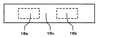
- the retardation film 16 is a retardation film made of a liquid crystalline polyimide containing a photoreactive group, and is a patterned retardation film. That is, the phase difference film 16 includes two regions 16a and 16b having different optical characteristics, and a region 16c that surrounds these regions and further has different optical properties. It is formed by irradiation with polarized light and baking.
- the regions 16a and 16b are regions where the retardation is 1 / 4 ⁇
- the region 16c is a region where the retardation is zero
- the regions 16a and 16b are oriented so that their optical axes are orthogonal to each other. .
- the linearly polarized light thus obtained has an optical axis that is plus or minus 45 degrees with respect to the transmission axis of the polarizing plate, and passes through a retardation film having a retardation of 1 / 4 ⁇ . It is converted into left circularly polarized light or right circularly polarized light depending on whether the optical axis of the retardation film is positive or negative.
- Such a combination of a polarizing plate and a 1 ⁇ 4 ⁇ plate is called a circularly polarizing plate because it selectively transmits only the left and right circularly polarized light components for a specific wavelength ⁇ of natural light.
- a circularly polarizing plate that selectively transmits left circularly polarized light is referred to as a left circularly polarizing plate
- a circularly polarizing plate that selectively transmits right circularly polarized light is referred to as a right circularly polarizing plate.
- the combination of the polarizing plate 17 and the patterned retardation film 16 with a region having a retardation of ⁇ can be the above-described circularly polarizing plate.
- the optical axes are orthogonal to each other in the regions 16a and 16b, in combination with the direction of the transmission axis of the special filter, that is, the polarizing plate, when the combination of the polarizing plate 17 and the region 16a is a left circular polarizing plate, The combination of the polarizing plate 17 and the region 16b is a right circular polarizing plate, and when the combination of the polarizing plate 17 and the region 16a is a right circular polarizing plate, the combination of the polarizing plate 17 and the region 16b is a left circular polarizing plate.
- the transmission axis of the polarizing plate 17 has an optical axis of the retardation film in the region 16a or the region 16b of the retardation film pattern being plus or minus 45 degrees.
- the combination of the polarizing plate 17 and the region 16a is a right circularly polarizing plate
- right circularly polarized light having a specific wavelength ⁇ is not reflected by the selective reflection film, so that the region corresponding to the region 16a is dark as shown in FIG. Become.
- the combination of the polarizing plate 17 and the region 16b becomes a left circularly polarizing plate, the left circularly polarized light having a specific wavelength ⁇ is reflected by the selective reflection film, and the region corresponding to the region 16b is not darkened.
- the combination of the polarizing plate 17 and the region 16b is a right circular polarizing plate
- the right circularly polarized light having a specific wavelength ⁇ is not reflected by the selective reflection film, so that the region corresponding to the region 16b is shown in FIG. Becomes darker.
- the combination of the polarizing plate 17 and the region 16a becomes a left circularly polarizing plate, the left circularly polarized light having a specific wavelength ⁇ is reflected by the selective reflection film, and the region corresponding to the region 16a is not darkened.
- the orientation of the liquid crystalline polyimide containing the photoreactive group in the retardation film 16 is not affected by the orientation of the mesogen skeleton in the selective reflection film 15, and the retardation films 16a and 16b
- the direction of the optical axis is controlled by a masking technique such as a photomask in the state of polyamic acid and the direction of the polarization axis of the linearly polarized light irradiated.
- a patterned retardation film 16 is formed on a support 18, a selective reflection film 15 is formed on the retardation film 16, and a selective reflection film 15 is formed. It can also be obtained by forming the pressure-sensitive adhesive layer 19 on top, bonding the selective reflection film 15 and the substrate 14 through the pressure-sensitive adhesive layer 19, and finally peeling the support 18.
- the liquid crystalline polyimide film containing the photoreactive group corresponding to the patterned retardation film 12 can also function as an alignment film of the liquid crystalline material of the selective reflection film 15.
- the surface of the retardation film 16 patterned with the liquid crystalline polyimide containing the photoreactive group is rubbed or irradiated with ultraviolet rays. It is also useful to apply.
- these anti-counterfeiting elements can be combined with optical elements of different principles such as holograms.
- a hologram sheet is added to the optical element, or an embossed hologram is formed on the surface of the selective reflection film 15 on the substrate 14 side in the anti-counterfeiting element of FIG.
- the anti-counterfeiting element in each of the above-described forms can be regarded as a pattern of differences in information regarding polarization.
- the difference in information regarding polarization is a latent image because it cannot be distinguished by the human eye.
- This latent image is passed through a special filter such as a polarizing plate, and the information regarding polarization is replaced with a difference in the amount of light that can be transmitted through the special filter. Recognized.
- a difference in information relating to polarization cannot be copied with a normal copying machine.
- the retardation film of the present invention can be suitably used for the retardation film 16 in the anti-counterfeiting element of FIG. 9, and as described above, labor can be saved in the production of such a retardation film and the above-described region can be easily used. In addition, it is superior to the case of using a conventional retardation film from the viewpoint of fine formation and excellent heat resistance.
- region where Re is zero can be formed by, for example, irradiating non-polarized light from the direction perpendicular
- the display device of the present invention is an image display device having a retardation film, and the retardation film of the present invention described above is included in part or all of the retardation film.
- the display device of the present invention can be configured by employing the above-described retardation film of the present invention as a part or all of the retardation film in the known image display device.
- a display device incorporating a patterned retardation film made of a liquid crystalline polyimide having a photoreactive group will be described.
- the stereoscopic image display device of FIG. 14 includes an image display device 20, a polarizing plate 21 disposed on the display surface of the image display device 20, and a retardation film 22 disposed on the polarizing plate 21. Has been.
- the image display device 20 is a display device that displays a two-dimensional image.
- the image display device 20 is a device that displays an image in each region divided into a plurality of rows in the row direction.
- the odd row 20a and the even row 20b are similar to the image to be displayed according to the parallax of the observer. It is a device that displays two types of images.
- a liquid crystal display, a plasma display, an organic EL display, or the like can be applied to the image display device 20.
- the image display device 20 displays a stereoscopic image, for example, an image for the left eye is displayed in the odd row 20a, and an image for the right eye is displayed in the even row 20b.
- the polarizing plate 21 is attached to the display surface of the image display device 20.
- the polarizing plate 21 has an absorption axis in one direction indicated by an arrow 21a.
- the retardation film 22 is attached to the polarizing plate 21.
- the phase difference film 22 is a film of liquid crystalline polyimide having a photoreactive group. Together with the polarizing plate 21, the left-eye image light from the odd-numbered rows 20a is converted into a specific polarization state (right circularly polarized light in FIG. 14), Optical axes or retardations corresponding to the odd-numbered rows 20a and even-numbered rows 20b so as to convert the image light for the right eye from the even-numbered rows 20b into a specific polarization state different from the polarization state (left-circularly polarized light in FIG. 14).
- a patterned retardation film in which two types of regions 22a and 22b having different parameters of at least one of the above are patterned.
- the retardation film 22 has the same retardation of 1 / 4 ⁇ in the regions 22a and 22b, but only the optical axis is ⁇ 45 degrees with respect to the absorption axis of the polarizing plate 21, +45 It is patterned to be a degree.
- the image light for the left eye emitted from the odd rows 20a of the image display device 20 passes through the polarizing plate 21, passes through the region 22a of the retardation film 22, and is converted into right circularly polarized light.
- the right-eye image light emitted from the even-numbered row 20b of the image display device 20 passes through the polarizing plate 21, passes through the region 22b of the retardation film 22, and is converted into left circularly polarized light.
- the observer passes only the left circularly polarized light through the polarizing filter 23a that passes only the right circularly polarized light through the special filter for the left eye that covers the field of view of the left eye 24a of the observer, and the special filter for the right eye that covers the field of view of the right eye 24b of the observer.
- the polarizing filter 23b is attached, the left eye 24a can capture only the image light for the left eye and the right eye 24b can capture only the image light for the right eye, and the observer can recognize a stereoscopic image.
- the polarizing plate 21 can be installed on the liquid crystal display together with the function of the polarizing plate originally provided on the viewer side of the liquid crystal display.
- a structure in which a non-patterned retardation film is separately added is also a preferred form of the stereoscopic image display device.
- the non-patterned retardation film can be installed at an arbitrary position between the polarizing plate 21 and the polarizing filters 23a and 23b.
- left and right circularly polarized light are listed as specific polarization states, but it is also preferable to apply a combination of linearly polarized light in which the vectors are orthogonal to each other as the specific polarization state.
- the retardation film 22 is formed by patterning a region where the retardation is 1 / 2 ⁇ , the optical axis is 45 degrees with respect to the absorption axis of the polarizing plate 21, and the region where the retardation is zero.
- the retardation film of the present invention can be suitably used for the retardation film 22 having a plurality of regions having different optical characteristics in the same film. As described above, labor saving of the production of such a retardation film can be achieved. From the viewpoint of easy formation of the region and excellent heat resistance, this is superior to the case of using a conventional retardation film.
- the liquid crystal display device of the present invention has the above-described retardation film of the present invention.
- the liquid crystal display device of the present invention can be constructed by using the retardation film of the present invention as a part or all of the retardation film in the configuration of a known liquid crystal display device.
- the liquid crystal display device of the present invention is superior to the case where a conventional retardation film is used from the viewpoint of labor saving in the production of the retardation film, easy formation of the region, and excellent heat resistance.
- the retardation film of the present invention is a liquid crystal display element composed of various layers.
- a liquid crystal display element can be configured by being provided at an arbitrary position.
- the retardation film of the present invention is excellent in that a fine pattern having different optical characteristics can be easily formed, and thus is preferably integrated with a color filter.
- a color filter layer having a specific spectral transmittance characteristic and a pattern for selectively transmitting light in a specific wavelength band using the principles such as absorption, interference, and scattering are formed. This substrate is called a color filter.
- the color filter forms two or more regions of a color filter layer having different spectral transmittance characteristics for each pixel unit in order to display an image in color.
- the color filter generally has a color filter layer having a spectral transmittance that selectively and independently transmits light in the red, blue, and green wavelength ranges.
- the wavelength band selectively transmitted in the color filter layer to be applied and the number of divisions into the sub-pixels are not limited.
- the color filter layer and the retardation film are provided close to or in contact with each other in consideration of the influence of parallax.
- the effect of parallax is a deviation of an optical path between a color filter layer and a corresponding retardation film region that may occur when the liquid crystal display device is viewed from an oblique direction. This is preferable from the viewpoint of preventing the loss of the effect due to the adjustment of the optical characteristics of the retardation film due to the deviation.
- liquid crystal display device of the present invention in subpixels divided by color filter layers having different spectral transmittance characteristics, light in a specific wavelength region is transmitted according to the spectral transmittance characteristics of the respective color filter layers.
- a phase difference film integrated with a color filter is a sub-pixel unit in which color filter layers having different spectral transmittance characteristics are formed, and a liquid crystal corresponding to a wavelength range in which light is transmitted or a wavelength representative of the wavelength range.
- the retardation and the optical axis angle can be optimized in accordance with an optical design that improves the characteristics of the display device.
- the wavelength representative of the wavelength range means any wavelength included in the wavelength range where the transmittance is high in the spectral transmittance characteristics of the color filter layer, but further, the spectrum of the backlight used in the liquid crystal display device. It may be set in consideration of characteristics and visibility.
- the retardation film of the present invention is provided with a region where a reflection plate is provided for each pixel unit (hereinafter also referred to as “reflection region”) and a reflection plate so that external light and a backlight can be used together as a light source.
- a transflective liquid crystal display device having a non-transparent region hereinafter also referred to as a “transmission region”.
- retardation and light of a retardation film are provided for each of the reflection region and the transmission region in accordance with the optical design of the reflection region and the transmission region.
- the shaft angle of the shaft can be optimized.
- the retardation film of the present invention is a transflective liquid crystal display device in which one or both of the retardation and the optical axis angle are adjusted so as to express desired optical characteristics in the reflective region and the transmissive region. Can be provided on the optical path from both the external light source and the backlight.
- the retardation film of the present invention can be used in a transflective liquid crystal display device in which a reflective region and a transmissive region are formed for each subpixel divided by color filter layers having different spectral transmittance characteristics.
- the retardation of the retardation film and the axis angle of the optical axis can be optimized in accordance with the optical design corresponding to the region and the wavelength representative of the corresponding color filter layer. That is, the retardation film of the present invention is a transflective liquid crystal display device having color filter layers having different spectral transmittance characteristics. The sub-pixels of the color filter layer having different spectral transmittance characteristics and the reflection of each sub-pixel are reflected.
- an area in which one or both of the retardation and the optical axis angle are adjusted so as to express desired optical characteristics is formed on the optical path from the reflection region and the transmission region of each color filter layer.
- the retardation film of the present invention can independently form a region having desired optical characteristics even in a region that is formed more finely so as to further divide a pixel.
- each layer such as an electrode and a liquid crystal alignment film is sequentially laminated on each of the illustrated substrates, and these substrates are opposed to each other, and a liquid crystal layer made of a driving liquid crystal medium is sandwiched and bonded.
- a liquid crystal layer made of a driving liquid crystal medium is sandwiched and bonded.
- the liquid crystal display device of FIG. 15 includes a planar substrate 31, a switching element 32 disposed on the planar substrate 31, an insulating film 33 disposed on the switching element 32, and a reflective electrode 34 disposed on the insulating film 33.
- the transparent electrode 38 disposed on the alignment film 37, the retardation film 39 disposed on the transparent electrode 38, the overcoat layer 40 disposed on the retardation film 39, and the overcoat layer 40.
- the reflective liquid crystal display device includes a color filter layer 41, a transparent substrate 42 disposed on the color filter layer 41, and a polarizing plate 43 disposed on the transparent substrate 42.
- the color filter layer 41 is a layer formed by dividing a layer that selectively transmits red, green, and blue light into three subpixels for each pixel, and the retardation film 39 has a photoreactive group. It is a film of liquid crystalline polyimide, and is a film in which a pattern composed of three regions each having different optical characteristics is formed according to the red, green, and blue color filter layers.
- the liquid crystal display device of FIG. 16 includes a planar substrate 31, a switching element 32 disposed on the planar substrate 31, an insulating film 33 disposed on the switching element 32, and a reflective electrode disposed on the insulating film 33.
- a liquid crystal alignment film 35 disposed on the reflective electrode 34
- a liquid crystal layer 36 composed of a driving liquid crystal medium disposed on the liquid crystal alignment film 35
- a retardation film 39 disposed on the liquid crystal layer 36
- Transparent electrode 38 disposed on retardation film 39 overcoat layer 40 disposed on transparent electrode 38, color filter layer 41 disposed on overcoat layer 40, and disposed on color filter layer 41
- the reflective liquid crystal display device includes a transparent substrate 42, a retardation film 44 disposed on the transparent substrate 42, and a polarizing plate 43 disposed on the retardation film 44.
- the retardation film 44 is a retardation film having uniform optical characteristics, for example, a retardation film composed of a retardation film made of a polymerizable liquid crystal material and a liquid crystal
- a backlight unit 45 as a light source
- a polarizing plate 46 disposed on an optical path from the backlight unit 45
- a transparent substrate 47 disposed on the polarizing plate 46
- a transparent substrate disposed on the polarizing plate 46
- a transparent substrate disposed on the polarizing plate 46
- Switching element 32 disposed on 47
- insulating film 33 disposed on switching element 32
- transparent electrode 48 disposed on insulating film 33
- liquid crystal alignment film 35 disposed on transparent electrode 48
- a liquid crystal layer 36 composed of a driving liquid crystal medium disposed on the liquid crystal alignment film 35, a liquid crystal alignment film 37 disposed on the liquid crystal layer 36, a transparent electrode 38 disposed on the liquid crystal alignment film 37, and a transparent electrode
- the phase difference film 49 disposed on the phase difference film 49, the phase difference film 39 disposed on the phase difference film 49, the overcoat layer 40 disposed on the phase difference film 39, and the overcoat layer 40.
- a color filter layer 41, a transmission type liquid crystal display device comprising a transparent substrate 42 disposed on the color filter layer 41, a polarizing plate 43 disposed on the transparent substrate 42.
- the retardation film 49 is a retardation film having uniform optical characteristics.
- the retardation film 49 is a retardation film made of a polymerizable liquid crystal material in which a polymerizable liquid crystal compound is aligned by the retardation film 39.
- a backlight unit 45 that is a light source
- a polarizing plate 46 disposed on an optical path from the backlight unit 45
- a retardation film 44 disposed on the polarizing plate 46
- a transparent substrate 47 disposed on the phase difference film 44
- a switching element 32 disposed on the transparent substrate 47
- an insulating film 33 disposed on the switching element 32
- a transparent electrode 48 disposed on the insulating film 33.
- a color filter layer 41, a transmission type liquid crystal display device comprising a transparent substrate 42 disposed on the color filter layer 41, a polarizing plate 43 disposed on the transparent substrate 42.
- the 19 includes a backlight unit 45 that is a light source, a polarizing plate 46 disposed on an optical path from the backlight unit 45, and a transparent substrate 47 disposed on the polarizing plate 46.
- the switching element 32 disposed on the transparent substrate 47, the insulating film 33 disposed on the switching element 32, the transparent electrode 48 and the reflective electrode 34 disposed on the insulating film 33, the transparent electrode 48 and the reflective electrode
- the transparent electrode 38 disposed on the transparent electrode 38, the cell thickness adjusting layer 50 disposed on the transparent electrode 38 on the reflective electrode 34, and the transparent electrode 38 on the transparent electrode 48 and the cell thickness adjusting layer 50 are disposed on the transparent electrode 38.
- the transparent electrode 48 and the reflective electrode 34 are arranged on the insulating film 33 in a predetermined pattern so that regions corresponding to the sub-pixels in each pixel are divided by these electrodes.
- the cell thickness adjusting layer 50 is a layer made of a resin having light transmissivity and disposed corresponding to a region corresponding to the reflective electrode 34 in a region corresponding to each subpixel.
- the phase difference film 51 is a film of liquid crystalline polyimide having a photoreactive group, and further in accordance with the transparent electrode 48 and the reflective electrode 34 in each of three regions having different optical characteristics according to each sub-pixel. It is a film having a pattern that forms two regions having different optical characteristics, that is, six regions having different optical characteristics in each pixel.
- liquid crystal display device there are two parallel substrates 31 and 42 arranged in parallel, at least one of which is transparent.
- a transparent electrode 38 and a liquid crystal alignment film 37 are formed on at least one substrate, and a transparent electrode 48 or a reflective electrode 34 and a liquid crystal alignment film 35 are formed on the other substrate as necessary.
- a backlight unit 45 is used as a light source.
- a liquid crystal display device is a transmissive liquid crystal display device. Called (FIGS. 17 and 18).
- a liquid crystal display device using external light as a light source is called a reflective liquid crystal display device.
- a reflector is required.
- a method of providing a reflector on the outside of the liquid crystal cell (not shown), and a reflector 34 combined with the function of the reflector and the electrode are provided in the liquid crystal cell.
- the latter is preferable because the influence of parallax is small.
- a liquid crystal layer 36 made of a driving liquid crystal medium is sandwiched between two opposing flat substrates 31 (47) and 42.
- the liquid crystal layer 36 exhibits at least two different alignment states depending on the voltage applied to the liquid crystal alignment films 35 and 37 and the opposing electrodes 34 (48) and 38.
- the liquid crystal cell composed of the substrate and the layers and films between them has these structures.
- the film or structure formed or disposed on the planar substrates 31 (47) and 42 when the film or structure formed or disposed on the planar substrates 31 (47) and 42 is on the liquid crystal layer 36 side, the film or structure is formed or installed inside the liquid crystal cell. In addition, when the film or structure formed or placed on the planar substrates 31 (47) and 42 is on the side opposite to the liquid crystal layer 36, the film or structure is formed on the outside of the liquid crystal cell. Expressed as placed.
- a switching element 32 represented by a TFT and a color filter layer 41 are formed so that an applied voltage can be adjusted for each pixel as necessary.
- the overcoat layer 40 and the insulating film 33 are provided accordingly.
- a transparent substrate 42 having a color filter layer 41 and further having an overcoat layer 40, a cell thickness adjusting layer 50, a black matrix (not shown) or the like formed thereon as necessary is provided with a color filter or a color filter.
- This is called a filter substrate.
- the color filter layer 41 has specific spectral transmittance characteristics for selectively transmitting a specific wavelength band using principles such as absorption, interference, and scattering.
- a light source called a backlight unit 45 and at least one polarizing plate 43 or 46 are provided outside the liquid crystal cell as necessary.
- the polarizing plate 43 or 46 is installed on the flat substrate 31 (47), 42 outside the liquid crystal cell.
- the retardation film 39 made of liquid crystalline polyimide containing a photoreactive group is formed on the planar substrates 31 (47) and 42 at a position sandwiched between the liquid crystal layer 36 and the polarizing plate 43 or 46.
- the patterned retardation film 39 is preferably formed inside the liquid crystal cell in consideration of the influence of parallax, and is disposed adjacent to the color filter layer 41 on the liquid crystal layer 36 side. It is more preferable that the overcoat layer 40 is formed on the color filter layer 41 formed on the transparent substrate 42 as necessary.
- a liquid crystal display device in which a region provided with a reflector and a region not provided with a reflector are formed for each pixel can use the backlight unit 45 and external light in combination as a light source.
- a liquid crystal display device is called a transflective liquid crystal display device.
- FIG. 19 shows a liquid crystal display device in which a pattern of the transparent electrode 48 and the reflective electrode 34 is formed for each pixel.
- the phase difference film 51 corresponds to the pattern of the reflective electrode 34 and the transparent electrode 48, that is, the region where the reflective plate is provided and the region where the reflective plate is not provided.
- the size of the retardation and the angle of the optical axis are optimized. Further, the region where the reflecting plate is provided or the region where the reflecting plate is not provided also corresponds to the color filter layer 41 having different spectral transmittance characteristics, and representative wavelengths ⁇ 1 , ⁇ 2 ,. It is a more preferable form that the size of retardation and the angle of the optical axis are further optimized at ⁇ k .
- the patterned retardation film 39 made of a liquid crystalline polyimide containing a photoreactive group is formed adjacent to the liquid crystal layer 36 (FIG. 16)
- the patterned retardation film 39 is a driving liquid crystal in the liquid crystal layer 36. It is also possible to serve as an alignment film for the medium. In this case, in order to readjust the alignment regulating force on the driving liquid crystal medium, it is also useful to subject the surface of the retardation film 39 made of liquid crystalline polyimide containing a photoreactive group to rubbing treatment or irradiation with ultraviolet rays.
- the optical function of the retardation film and the driving liquid crystal are substantially the same as in the case where the alignment film is provided using a conventional alignment agent.
- a film having a function of orienting the medium can be obtained, and this is an advantage of the liquid crystalline polyimide containing a photoreactive group.
- a structure in which a non-patterned retardation film 44 or 49 is added separately is also a preferred embodiment.
- the non-patterned retardation film 44 or 49 is provided on the planar substrate 31 (47) or 42 at a position sandwiched between the liquid crystal layer 36 and the polarizing plate 43 or 46. Further, it is disposed either on the outside of the liquid crystal cell or on the inside of the liquid crystal cell.
- the retardation film formed inside the liquid crystal cell is not only a liquid crystalline polyimide containing a photoreactive group, but also a liquid crystalline material such as a polymerizable liquid crystal material or a lyotropic liquid crystal material, or a thin film formed by a solvent casting method.
- a polyamideimide resin or a polyetheretherketone resin having a specific structure in which a phase difference film having an optical axis in the thickness direction of the thin film can be obtained from the spontaneous orientation of the molecules in the evaporation process of the solvent.
- a polyimide resin In the process of evaporating the solvent, a polyamideimide resin or a polyetheretherketone resin having a specific structure in which a phase difference film having an optical axis in the thickness direction of the thin film can be obtained from the spontaneous orientation of the molecules in the evaporation process of the solvent.
- a polyimide resin In the process of evaporating the solvent, a polyamideimide resin or a polyetheretherketone
- the patterned retardation film 39 is made of a retardation film. It is also possible to serve as an alignment film of the liquid crystal material in 49. In this case, it is also useful to subject the surface of the retardation film 39 made of liquid crystalline polyimide containing a photoreactive group to rubbing treatment or irradiation with ultraviolet rays in order to readjust the alignment regulating force on the liquid crystalline material.
- an optical film called a retardation film is manufactured in almost the same manufacturing process as that in the case of providing an alignment film using a conventional alignment agent.
- a film having both the function of aligning the liquid crystalline material and the function of aligning the liquid crystalline material can be obtained. This is the advantage of the liquid crystalline polyimide containing a photoreactive group.
- the patterned retardation film 39 made of liquid crystalline polyimide containing a photoreactive group is formed inside the liquid crystal cell, an unpatterned retardation film is further formed on the patterned retardation film 39 (51).
- the film 49, the transparent electrode 38, the liquid crystal alignment film 37, and the cell thickness adjusting layer 50 may be arbitrarily formed.
- the process for forming these films and layers involves a thermal load in which a high processing temperature exceeding 200 ° C. is applied for a certain period of time.
- the retardation film 39 (51) made of a liquid crystalline polyimide containing a photoreactive group is excellent in heat resistance and has little change in properties such as retardation with respect to a thermal load caused by the previous process. This point is also an advantage of the liquid crystalline polyimide containing a photoreactive group.
- the retardation film of the present invention can be used for various optical elements having a retardation film other than the above-described embodiments.
- An example of such an optical element is a polarization hologram.
- Such a polarization hologram can be constructed by replacing the retardation film composed of a liquid crystal layer and a liquid crystal alignment layer in a known polarization hologram with the retardation film of the present invention, for example, as disclosed in JP-A-2008-532085.
- the photo-alignment layer (2) and the liquid crystal composition (3) shown in FIG. 1 can be replaced with the retardation film of the present invention.
- ⁇ Viscosity> It measured using the rotational viscometer (TV-22L, the Toki Sangyo company make) of a polyamic acid solution.
- a gel permeation chromatograph system (PU-2080 HPLC pump, 865-CO column oven, UV-2075 UV-visible detector, RI-2031 differential refractometer detector) manufactured by JASCO Corporation is used for GPC, and Shodex GF is used for the column. -7MHQ (made by Showa Denko) was used.
- ⁇ Thickness of retardation film> A part of the retardation film was shaved from the substrate on which the retardation film was formed, and the level difference was obtained by measuring a surface measurement profiler (Alphastep IQ / manufactured by KLA Tencor Corporation).
- 1,8-bis (3,4-dicarboxyphenyl) octane tetraethyl ester (43 g, 77 mmol) was dissolved in ethanol (250 mL), 5.7% aqueous sodium hydroxide solution (250 mL) was added, and the mixture was refluxed for 2 hours. After the reaction, the solvent was distilled off under reduced pressure, and concentrated hydrochloric acid was added until the pH reached 1. After the produced precipitate was filtered, the precipitate was washed three times with pure water (200 mL). The obtained crystals were dried under reduced pressure to obtain 1,8-bis (3,4-dicarboxyphenyl) octane. Yield 31 g, yield 90%.
- the solution (A-1) was applied to a glass substrate with a spinner (2,000 rpm, 15 seconds), further heated at 80 ° C. for 3 minutes to evaporate the solvent, and then irradiated with ultraviolet rays through a polarizing plate.
- Linearly polarized polarized ultraviolet rays (illuminance: 9 mW / cm 2 , irradiation energy intensity: 5 J / cm 2 ) were irradiated.
- the substrate irradiated with polarized ultraviolet rays was heat-treated in an oven at 230 ° C. for 15 minutes to obtain a retardation film 1 having a thickness of 175 nm.
- the retardation film 1 is made of polyimide having liquid crystallinity obtained by heating and imidizing a polyamic acid having a photoreactive group. The film was confirmed.
- the direction of the optical axis in the retardation film 1 is substantially parallel to the direction of the absorption axis of the polarizing plate when irradiated with polarized ultraviolet rays, and the angle of the optical axis in the retardation film 1 is controlled by the polarization state of the irradiated ultraviolet rays. I confirmed that I can do it.
- the direction of the optical axis of the retardation film 1 was confirmed by measurement with an ellipsometer (manufactured by OptiPro / Shintech Co., Ltd.).
- ⁇ Test of heat resistance of retardation film 1> The retardation film 1 was left in an oven at 230 ° C. for 2 hours, taken out of the oven, returned to room temperature, and measured for retardation. As a result, the change was 1 nm as compared with that before putting into the oven at 230 ° C. Was less than. From the above, it was confirmed that the retardation film 1 was excellent in heat resistance.
- Example 2 ⁇ Preparation of polymerizable (cholesteric) liquid crystal material solution (B-1) for obtaining a green selective reflection film>
- the following compound (P-1) 82.2 wt%, the following compound (P-2) 4.8 wt%, the following compound (P-3) 9.7 wt%, and the following compound (P-4) 3.3
- the composition consisting of% by weight is defined as (MIX1), CPI-110P (San Apro Co., Ltd.) with a weight ratio of 0.030 is added to this (MIX1), and cyclopentanone with a weight ratio of 2.333 is further added.
- a solution (B-1) of 30% by weight of cyclopentanone was obtained.
- Compound (P-1) was synthesized by the method described in Macromolecules, 1993, 26 (6), 244.
- Compound (P-2) and Compound (P-3) were synthesized by the method described in JP-A-2005-60373.
- compound (P-4) was synthesized by the method described in JP-A-2005-263778.
- the polymerizable (cholesteric) liquid crystal material has an alignment in which the spiral axis is aligned in the normal direction of the substrate, and the retardation film 1 also has a function of aligning the polymerizable (cholesteric) liquid crystal material. .
- Example 3 ⁇ Preparation of a solution (B-2) of a polymerizable liquid crystal material having a rod-shaped mesogen skeleton that can fix a homogeneous alignment and obtain a positive A plate>
- a composition composed of 75% by weight of the following compound (P-5) and 25% by weight of the following compound (P-6) is referred to as (MIX2), and this (MIX2) is Irgacure 907 (Ciba Japan Co., Ltd.) having a weight ratio of 0.03. Company) and cyclopentanone in a weight ratio of 2.333 were added to obtain a cyclopentanone solution (B-2) having a solute concentration of 30% by weight.
- Compound (P-5) was synthesized by the method described in JP-A-2006-307150.
- Compound (P-6) was synthesized by the method described in Macromolecules, 1990, 23 (17), 3938.
- Phase difference film (II) A retardation film (II) was produced in the same manner as the retardation film (I), except that the irradiation energy intensity of polarized ultraviolet light to the film of the solution (A-2) before firing was 2.6 J / cm 2 .
- the film thickness of the obtained retardation film (II) was 83 nm.
- the retardation of the retardation film (II) was measured in the same manner as the retardation film (I).
- the retardation of the retardation film (II) is shown in the following table.
- Phase difference film (III) Using the rubbing device RM-50 manufactured by Eetchy Co., Ltd., the retardation film (I) is pushed into the rubbing cloth (hair length 1.8 mm: rayon): 0.6 mm Rolling speed of the roller: 1 , 400 rpm, stage moving speed: rubbed in one direction under conditions of 0.6 m / min, and the solution (B-2) was applied thereon with a spinner at 1,800 rpm for 15 seconds. After the coating film was heated at 80 ° C. for 3 minutes to evaporate the solvent, the obtained coating film was fixed by irradiating with ultraviolet rays (illuminance: 25 mW / cm 2 , irradiation amount: 0.75 J / cm 2 ).
- a retardation film made of a polymerizable liquid crystal material horizontally aligned on the retardation film (I) was produced on a substrate.
- This retardation film is referred to as a retardation film (III).
- the total thickness of the obtained retardation film (III) was 775 nm.
- the retardation of the retardation film (III) was measured in the same manner as the retardation film (I).
- the retardation of the retardation film (III) is shown in the following table.
- Phase difference film (IV) The phase difference film (II) is rubbed in the direction parallel to the slow axis under the same conditions as those for the preparation of the phase difference film (III), and the solution is formed thereon under the same conditions as for the preparation of the phase difference film (III).
- B-2 was applied and fixed, and a retardation film made of a polymerizable liquid crystal material horizontally aligned on the retardation film (II) was produced on a substrate.
- This retardation film is referred to as a retardation film (IV).
- the thickness of the obtained retardation film (IV) was almost the same as the thickness of the retardation film (III) and was 779 nm. Further, the retardation of the retardation film (IV) was measured in the same manner as the retardation film (I).
- the retardation of the retardation film (IV) is shown in the following table.
- Phase difference film (V) The retardation film (II) is rubbed in the direction perpendicular to the slow axis under the same conditions as those for the preparation of the retardation film (III), and the solution ( B-2) was applied and fixed, and a retardation film made of a polymerizable liquid crystal material horizontally aligned on the retardation film (II) was produced on a substrate.
- This retardation film is referred to as a retardation film (V).
- the thickness of the obtained retardation film (V) was almost the same as the thickness of the retardation film (III) and was 772 nm. Further, the retardation of the retardation film (V) was measured in the same manner as the retardation film (I).
- the retardation of the retardation film (V) is shown in the following table.
- a blue pixel having a color filter layer that selectively transmits light having a wavelength of blue (near 450 nm) and a light having a wavelength of green (near 550 nm) are selected.
- a liquid crystal display device having a green pixel having a transparent color filter layer, a red pixel having a color filter layer that selectively transmits light having a wavelength of red (near 650 nm), and a pattern thereof is assumed.
- retardation or retardation film of liquid crystalline polyimide containing a photoreactive group whose optical axis is not patterned, and a retardation film corresponding to a positive A plate made of a polymerizable liquid crystal material were formed thereon. Let's look at the characteristics of the composite retardation film.
- a composite retardation film (V) corresponding to a blue pixel, a composite retardation film (III) corresponding to a green pixel, and a composite retardation film (IV) corresponding to a red pixel When selected, from the evaluation results of the composite retardation films (III) to (V), the retardation at a wavelength of 450 nm, which is typical for blue pixels, is obtained as a characteristic of the composite retardation film corresponding to the blue, green, and red pixels.
- a retardation film that can obtain such a relationship is obtained by, for example, applying the solution (A-2) to a color filter layer in which blue, red, and green colored layers are patterned, Through a mask having a pattern corresponding to the colored layer, the polarized colored ultraviolet ray is irradiated with an appropriate irradiation energy intensity in a predetermined polarization direction so that the polyimide is oriented in a direction perpendicular to the subsequent rubbing direction, and the red colored layer
- the coating film is baked by irradiating polarized ultraviolet rays with an appropriate irradiation energy intensity in a predetermined polarization direction so that the polyimide is oriented in a direction parallel to the subsequent rubbing direction through a mask having a pattern corresponding to A liquid crystalline polyimide film is formed, and the obtained film is rubbed in one specific direction as described above, and the solution (B-2) is applied to the surface of the rubbed film and fixed to be horizontally aligned polymerizable liquid crystal material.
- Table 8 shows the retardation film formed of each material used in these calculations and the wavelength dependency of ⁇ n.
- pA-plate (I) represents a positive A-plate retardation film made of a liquid crystalline polyimide having a photoreactive group, and the wavelength dependency of ⁇ n is shown in Table 4 of Example 3. Based. Also, the axis angle of the optical axis given by each optical calculation and the magnitude of the retardation Re are based on the results of the previous embodiment, the direction of polarized ultraviolet rays when forming the retardation film, the irradiation energy intensity, the film thickness It is a value obtained by optimizing parameters such as.
- pA-plate (II) represents a positive A-plate retardation film made of a homogeneously aligned polymerizable liquid crystal material, and the wavelength dependence of ⁇ n is based on the results of Table 5 in Example 3. .
- the size of the retardation Re given in each optical calculation is a value within the range obtained by optimizing parameters such as the film thickness when forming the retardation film based on the result of the previous embodiment. It is.
- nC-plate represents a negative C-plate retardation film made of a helically aligned polymerizable liquid crystal material
- the wavelength dependency of ⁇ n is a composition described in JP-A-2005-263778 and the like. This is a value obtained by preparing and measuring a film of an object.
- the magnitude of the retardation Rth given by each optical calculation is a value obtained by optimizing parameters such as the film thickness when the retardation film is formed.
- the retardation film is based on a cyclic olefin-based resin stretched under specific conditions, and the wavelength dependency of ⁇ n is obtained by peeling the retardation film from a commercially available liquid crystal display and measuring it. Value.
- size of retardation Re given by each optical calculation is a value obtained by optimizing parameters, such as a film thickness at the time of film-forming a retardation film, and extending
- the polarizing plate protective layer is made of a cellulose resin bonded to a commercially available polarizing plate, and the wavelength dependency of the retardations Rth and ⁇ n is more polarized than the polarizing plate mounted on a commercially available liquid crystal display. It is a value obtained by peeling and measuring only the plate protective layer.
- the driving liquid crystal is a liquid crystal composition developed for the VA mode, and the wavelength dependence of ⁇ n (the difference between the extraordinary refractive index ne and the ordinary optical refractive index no) is shown in Table 8.
- the retardation Rth of the VA cell is the product of the difference between the ordinary light refractive index no and the extraordinary light refractive index ne and the cell thickness d, and the retardation Rth given in each optical calculation can be obtained by controlling the cell thickness d. Value.
- the axis angle of the optical axis of the optical element and the retardation film applied thereto, retardation Re, Rth, and the axis angle of the absorption axis of the polarizing plate are as defined above. Further, when evaluating the optical characteristics of the anti-counterfeiting element and the optical element of the liquid crystal display device, the angle formed by the optical element and the direction of the observer's line of sight is expressed in polar coordinates (azimuth angle ( ⁇ ), polar angle ( ⁇ )) The definition is shown in FIG.
- the display surface of the anti-counterfeiting element or the liquid crystal display device is the XY plane, the surface including the line-of-sight direction is the incident surface, and the angle formed by the X axis and the incident surface is the azimuth angle ( ⁇ ). Is the polar angle ( ⁇ ).
- Example 4 Wavelength dependence according to Table 4 of Example 3, in which a plurality of patterns having different optical axis angles and retardation sizes are formed on a mirror-like reflector using a liquid crystalline polyimide having a photoreactive group
- An optical element on which a pA-plate retardation film (pA-plate (I)) having s is formed is referred to as a forgery prevention element (1).
- This retardation film is applied to the coating film of polyamic acid with a uniform and uniform film thickness by applying polarized UV irradiation with the optimal orientation and irradiation energy intensity for each predetermined area together with masking with a photomask.
- a plurality of patterns AI to A-VI having different optical axis angles and retardation sizes are formed.
- phase difference film having a uniform optical axis angle and retardation of a homogeneously aligned polymerizable liquid crystal material is used.
- An optical element having a structure in which (-plate (II)) is formed is defined as an anti-counterfeit element (2).
- This phase difference film is formed by rubbing the surface of pA-plate (I) in one direction so that a desired slow axis can be obtained, and the film thickness is optimized according to the desired retardation.
- a film of a polymerizable liquid crystal material in which the orientation is fixed, and a plurality of patterns BI to B having different optical characteristics according to the patterns AI to A-VI formed in pA-plate (I) -VI is formed.
- the structure of the anti-counterfeit element (1) and the anti-counterfeit element (2) is in accordance with the structure shown in FIG.
- the chromaticity and relative reflectance are almost the same regardless of the angle of the optical axis and retardation of the retardation film. Cannot be identified.
- a polarizing plate on which a retardation film having a specific retardation Re size is bonded is referred to as a special filter, and a polarizing plate on which a retardation film having a retardation of 138 nm is bonded is designated as filter I, the retardation of 530 nm.
- the polarizing plate with which the phase difference film was bonded be filter II.
- Tables 9 and 10 show the optical characteristics and observation results of each forgery prevention element.
- the retardation film and the polarizing plate are bonded so that the direction of the absorption axis of the polarizing plate is 45 ° when the direction of the optical axis of the retardation film is 0 °.
- the observation with the filter is performed by arranging the filter so that the retardation film is on the anti-counterfeiting element side, and the chromaticity and the relative reflectance are observed with both the azimuth angle and the polar angle at 0 °. Value.
- the retardation film of the present invention can constitute a forgery prevention element in which a specific color is observed through the filter.
- the retardation film of the present invention has a coating film of the polyamic acid solution having a type of irradiation light, a polarization direction, and an irradiation energy intensity through a mask having an opening corresponding to a part of a character or a pattern.
- Example 5 ⁇ Characteristics of Circular Polarizing Plate Combining 1 / 4 ⁇ Plate and Polarizing Plate by Pattern Retardation Film Optimizing Retardation and Optical Axis for Blue, Green, and Red Pixels and Composite Retardation Film Containing This Retardation Film>
- a quarter ⁇ plate is combined with a polarizing plate to form a circular polarizing plate, which is placed on a reflecting plate, the reflectance of reflected light is calculated, and the performance of the circular polarizing plate is evaluated.
- this circularly polarizing plate is used in a reflective liquid crystal display device or a transflective liquid crystal display device, the reflective plate and the polarizing plate have spectral transmittances corresponding to blue, green, and red. A pattern of the color filter layer is formed.
- an A-plate retardation film made of a homogeneously aligned polymerizable liquid crystal having a uniform optical axis angle and retardation size, regardless of blue, red and green pixels.
- the case of (II)) is referred to as Comparative Example 1.
- the case of I) is referred to as Invention Example 1.
- the retardation film (pA-plate (I)) has a retardation for each pixel of blue, green, and red, together with masking with a photomask on a polyamic acid coating film having a uniform film thickness on the entire surface.
- a pattern in which the size of the retardation is optimized is formed for each pixel of blue, green, and red.
- the retardation film (pA-plate (I)) is optimal for each pixel of blue, green, and red together with masking with a photomask on a polyamic acid coating film having a uniform film thickness on the entire surface.
- a pattern in which the direction of the optical axis and the size of the retardation are optimized is formed for each pixel of blue, green, and red.
- the retardation film (pA-plate (II)) is rubbed in one direction on the surface (reflector side) of the retardation film (pA-plate (I)) so as to obtain a desired slow axis.
- It is a film of a polymerizable liquid crystal material that is formed and has a homogeneous alignment fixed with the film thickness optimized in accordance with the retardation.
- the reflectance of Comparative Example 1 is 1.97 ⁇ 10 ⁇ 3
- the reflectance of Invention Example 1 is 6.57 ⁇ 10 ⁇ 4
- the reflectance of Invention Example 2 is 4. It was 33 ⁇ 10 ⁇ 4 .
- the 1 / 4 ⁇ plate is blue.
- Example 6 ⁇ Improvement of viewing angle characteristics of VA mode by a retardation film with optimized retardation and optical axis for each pixel of blue, green, and red and a composite retardation film including the retardation film>
- a VA mode transmissive liquid crystal display device optically compensated by positive A-plate and negative C-plate was evaluated.
- a pattern of a color filter layer having spectral transmittance corresponding to blue, green, and red is formed, and pA-plate (I), pA-plate (II), and nC-plate are all on the color filter layer. It is formed on the driving liquid crystal medium side.
- an A-plate phase difference film made of a homogeneously aligned polymerizable liquid crystal material having a uniform optical axis angle and retardation size irrespective of blue, red and green pixels.
- plate (II)) is referred to as Comparative Example 2 and Comparative Example 3.
- the positive A-plate is a retardation film (pA-plate (I)) in which the size of the retardation is optimized using a liquid crystalline polyimide containing a photoreactive group and the pattern is formed
- the retardation film (pA-plate (I)) has a retardation for each pixel of blue, green, and red, together with masking with a photomask on a polyamic acid coating film having a uniform film thickness on the entire surface.
- a liquid crystal polyimide containing a photoreactive group is used to optimize the axial angle of the optical axis and the size of the retardation, and the phase difference in which the pattern is formed A film (pA-plate (I)) and an A-plate retardation film (pA-plate (II)) made of a homogeneous alignment polymerizable liquid crystal material having a uniform optical axis angle and a retardation size.
- the combined cases are designated as Invention Examples 3, 4, and 6.
- the retardation film (pA-plate (I)) is optimal for each pixel of blue, green, and red together with masking with a photomask on a polyamic acid coating film having a uniform film thickness on the entire surface.
- a pattern in which the direction of the optical axis and the size of the retardation are optimized is formed for each pixel of blue, green, and red.
- the retardation film (pA-plate (II)) has a uniform surface (polarizing plate protective layer side or driving liquid crystal side) of the retardation film (pA-plate (I)) so that a desired slow axis can be obtained. It is a film of a polymerizable liquid crystal material formed by rubbing in the direction and further fixing a homogeneous alignment whose film thickness is optimized in accordance with the retardation.
- the directions of the absorption axes of the first and second polarizing plates, the first and second polarizing plate protective layers, the VA cell, the Rth of nC-plate, the Re of each pA-plate, and the The luminance in the viewing angle direction in the example is shown in the following table.
- the spectral transmittance characteristics of Comparative Example 3 and Invention Example 6 are shown in FIG.
- the Rth of the VA cell is obtained by (no ⁇ ne) ⁇ d, where no and ne represent the refractive index of the driving liquid crystal layer, and d represents the thickness of the driving liquid crystal layer.
- a positive A-plate As a positive A-plate, a positive A-plate is used as compared with the case where a retardation film having a uniform optical axis angle and retardation is used regardless of blue, red and green pixels (Comparative Examples 2 and 3).
- a phase difference film with a pattern formed by optimizing the angle of the optical axis and the size of retardation using a liquid crystalline polyimide containing a photoreactive group for each pixel of blue red and green Inventive Example 3 for Comparative Example 2 or Inventive Examples 4, 5, and 6 for Comparative Example 3 have lower luminance as shown in Table 12. This is because the transmittance is suppressed in a wider wavelength range as shown in FIG.
- the retardation film of the present invention uses a liquid crystalline polyimide film having a photoreactive group, it can be obtained by irradiating light with a specific polarization state, that is, a conventional alignment film and a polymerizable liquid crystal. Compared with the manufacturing method of the phase difference film by liquid crystalline materials including a material, it can provide with fewer member points and processes.
- the retardation film of the present invention can be adjusted by controlling the polarization state and irradiation energy intensity of the light that irradiates the axial angle of the optical axis and the magnitude of birefringence, by using a masking technique in combination, The optical axis and retardation can be changed for each predetermined region.
- a retardation film in which regions having different optical characteristics of the optical axis and retardation are patterned, a liquid crystal display device using the same, and an optical element such as an anti-counterfeiting element can be provided by a simplified manufacturing process.
Abstract
Description
液晶性ポリイミドとは、液晶性ポリイミドの主鎖あるいは側鎖に光反応性基を有し、かつサーモトロピック液晶性あるいはライオトロピック液晶性等の液晶性を示すポリイミドの総称である。以下に液晶性ポリイミドの具体的な構造を例示するが、以下の具体例は本発明の範囲を限定するものではない。
次に本発明の光反応性基を有する液晶性ポリイミドの具体例を示す。好ましい例としては、光反応性基を主鎖に有するポリアミック酸及びこれの脱水反応によって得られるポリイミドから選択される少なくとも1つのポリマーを含有する組成物であって、100℃から300℃の間に液晶温度範囲を有することを特徴とするものである。このような特徴が得られるポリアミック酸を構成するジアミンと酸無水物の化合物を表1に、その組み合わせの例を表2に示す。


本発明では、液晶性ポリイミド又はその前駆体を含有する、前記塗膜を形成するための材料に、液晶性ポリイミドの液晶性が得られる範囲で、液晶性ポリイミド又はその前駆体以外の材料(以下、「添加剤」とも言う)をさらに含有させることができる。添加剤は一種でも二種以上でもよい。例えば、前記液晶性ポリイミド又はその前駆体が上記に挙げた4つのポリアミック酸である場合では、液晶性ポリイミドにおいて100℃から300℃の間に液晶温度範囲を有する特徴が得られる範囲で、前記ポリアミック酸100重量部に対して添加剤を、前記材料に総量で50重量部未満まで含有させることができる。
本発明では、前記添加剤として、前記材料に、光反応性基を全く含まないポリアミック酸を含有させてもよい。このようなポリアミック酸としては、例えば直鎖状のポリアミック酸や、側鎖構造を有するポリアミック酸が挙げられる。これらのポリアミック酸は、例えば、得られる位相差膜を駆動液晶媒体又は液晶性材料の配向膜としても活用する上で、膜の電気特性や配向特性を改善し、又は液晶の配向特性を向上あるいは変化させる観点から添加することができる。
また本発明では、前記添加剤として、前記材料に、液晶性を向上させる観点から、非ポリイミド系液晶高分子を含有させてもよい。液晶高分子の例としては、Handbook of Liquid Crystals Vol.3 (出版:WILEY-VCH 1998年出版)に記載されているような、主鎖型サーモトロピック液晶高分子、側鎖型サーモトロピック液晶高分子等が挙げられる。
また本発明では、前記添加剤として、前記材料に、液晶性を向上させる等の観点から、重合性官能基を有する液晶性化合物を含有させてもよい。このような重合性液晶化合物の具体例を以下に例示する。


また本発明では、前記添加剤として、前記材料に、特性の経時劣化や環境による劣化を防ぐ観点から、ポリアミック酸のカルボン酸残基と反応する官能基を2つ以上有する化合物、いわゆる架橋剤をさらに含有させてもよい。このような架橋剤としては、例えば特許第3049699号公報、特開2005-275360号公報、特開平10-212484号公報等に記載されているような多官能エポキシ、イソシアネート材料が挙げられる。
また本発明では、前記添加剤として、前記材料に、ガラス基板への密着性を調節する観点から、有機ケイ素化合物をさらに含有させてもよい。有機ケイ素化合物としては、例えば、アミノプロピルトリメトキシシラン、アミノプロピルトリエトキシシラン、ビニルトリメトキシシラン、N-(2-アミノエチル)-3-アミノプロピルメチルジメトキシシラン、N-(2-アミノエチル)-3-アミノプロピルトリメトキシシラン、ビニルトリエトキシシラン、3-メタクリロキシプロピルトリメトキシシラン、3-グリシドキシプロピルトリメトキシシラン、3-グリシドキシプロピルメチルジメトキシシラン、2-(3,4-エポキシシクロヘキシル)エチルトリメトキシシラン等のシランカップリング剤、及びジメチルポリシロキサン、ポリジメチルシロキサン、ポリジフェニルシロキサン等のシリコーンオイルが挙げられる。有機ケイ素化合物の添加量は、前記液晶性ポリイミド又はその前駆体100重量部に対して0.01~5重量部であることが好ましく、0.1~3重量部であることがより好ましい。
また本発明では、前記材料には、所望により各種の添加剤をさらに含有させてもよい。例えば、前記材料には、塗布性のさらなる向上を望むときには、かかる目的に沿った界面活性剤を、帯電防止のさらなる向上を望むときは帯電防止剤を、重合性液晶化合物あるいは、架橋剤を含有させる場合、その重合反応あるいは架橋反応を促進させるために、重合開始剤を適量含有させてもよい。
以下、前記液晶性ポリイミド又はその前駆体、及び前述の添加剤を含む材料を位相差膜用材料と称す。
位相差膜用材料は、これを溶解させる能力を有する溶剤に溶解させた形態で使用することができる。以下、このような形態を位相差膜用材料溶液と称す。かかる溶剤はポリアミック酸又はその誘導体の製造や使用において通常使用されている溶剤を広く含み、使用目的に応じて、適宜選択できる。これらの溶剤を例示すれば以下のとおりである。
(1)前記位相差膜用材料溶液を刷毛塗り法、浸漬法、スピンナー法、スプレー法、印刷法、インクジェット法等により基板上に塗布する。
(2)基板上に形成された塗膜を50~120℃、好ましくは80~100℃で加熱し、溶剤を蒸発させる。
(3)任意の偏光状態の光を前記塗膜に照射して前記塗膜中のポリアミック酸を配向させる。
(4)ポリアミック酸を配向させた前記塗膜を150~300℃、好ましくは180~250℃で加熱しイミド化させるとともに、液晶相を発現させる。
光軸あるいはレタデーションを特定の領域でパターン化させる手法について説明する。具体的な手法は以下の3つが挙げられる。
任意の偏光状態は、直線偏光、円偏光、楕円偏光、無偏光より選択される特定の偏光状態である。前記ポリアミック酸の塗膜に所定の偏光状態の光が照射されることで、位相差膜における光軸の方向やレタデーションの大きさが制御される。加熱イミド化する前の、ポリアミック酸の膜に対して、フォトマスク等のマスキング技術と共に、異なる任意の偏光状態の光を複数回照射し、その後一気にイミド化、液晶相を発現する温度まで加熱することにより、所定の領域毎に光軸の方向やレタデーションの大きさが異なるパターン化した位相差膜が得られる。
前記ポリアミック酸の塗膜に任意の偏光状態の光が異なる照度もしくは照射エネルギー強度で照射されることで位相差膜におけるレタデーションの大きさを制御する。加熱イミド化する前の、ポリアミック酸の膜に対して、フォトマスク等のマスキング技術と共に、照度あるいは照射エネルギー強度を変えて任意の偏光状態の光を照射して、その後一気にイミド化、液晶相を発現する温度まで加熱することにより、所定の領域毎にレタデーションの大きさが異なるパターン化した位相差膜が得られる。
前記ポリアミック酸の塗膜の膜厚を変化させることで、位相差膜におけるレタデーションの大きさを制御する。塗膜の領域毎の厚さは、例えばインクジェット法等の、同一の膜中の特定の領域に選択的に(濃度、粘度、あるいは組成等が異なる)位相差膜用材料溶液を塗布することができる方法で塗膜を形成することによって変えることができる。
本発明の光学素子は、前述した本発明の位相差膜を有する。本発明における光学素子は、前述した本発明の位相差膜を少なくとも一層有していればよく、本発明の位相差膜を複数層有していてもよいし、光反応性基を含有する液晶性ポリイミドより形成される位相差膜とは別に、光反応性基を含有する液晶性ポリイミド以外の材料より形成される位相差膜を含んでもよい。また本発明の光学素子が有する本発明の位相差膜の種類は特に限定されない。
はじめに、図1に従って位相差膜の屈折率の異方性を、直交座標系を用いて説明する。位相差膜の平面に対して平行かつ互いに直交する軸をx軸及びy軸とし、位相差膜の表面に対して垂直な軸をz軸としたときの位相差膜の屈折率は、各軸に平行な方向に分解することができる。x、y、及びz軸のそれぞれに対応して分解した屈折率をそれぞれnx、ny、及びnzとし、位相差膜の厚さをdとする。本件では、nx≠nyである時、nx>nyであるとする。このとき、位相差膜の平面方向におけるレタデーション(Re)は、(nx-ny)×dで表わされ、位相差膜の平面に対して垂直な方向におけるレタデーション(Rth)は、[{(nx+ny)/2}-nz]×dで表わされる。また位相差膜の複屈折はnx-ny(=Δn)で表わされる。
次に、位相差膜の光軸や偏光板の吸収軸の軸角度を定義する。X軸、Y軸は位相差膜や偏光板の膜平面に平行な面であるXY平面の軸に相当し、位相差膜や偏光板の膜平面の法線に平行な軸がZ軸である。位相差膜が後述のAプレートである場合、その光軸はAプレートがポジティブAプレートである場合はx軸に相当し、AプレートがネガティブAプレートである場合はy軸に相当する。図2に示すように、光軸がX軸に対して平行ではない場合、光軸の軸角度1は、光軸とX軸がなす角度で表され、反時計回りに正に増加するように表示される。また、位相差膜が後述のCプレートである場合、光軸であるz軸はZ軸に平行である。偏光板の吸収軸の軸角度2は、偏光板の吸収軸とX軸がなす角度で表され、反時計回りに正に増加するように表示される。
三軸方向の屈折率の関係として、nx>ny=nzを有する。正の一軸性を示し、光軸が位相差膜の薄膜面に対して平行な位相差膜と表現される場合もある。環状オレフィン系樹脂や変性ポリカーボネート樹脂等の固有複屈折率が正の透明樹脂を特定の条件で延伸することで得られる。あるいは、棒状のメソゲン骨格を有する液晶性材料のダイレクタが一様なホモジニアス配向を透明な基材上に形成し固定化することでも得られる。棒状のメソゲン骨格を有する重合性液晶材料を水平配向させる例としては特開2006-307150号公報等に記載されている。
三軸方向の屈折率の関係として、nx=ny>nzを有する。負の一軸性を示し、光軸が位相差膜の薄膜面の法線方向と一致する位相差膜と表現される場合もある。環状オレフィン系樹脂、ポリカーボネート樹脂、セルロース系樹脂、アクリル系樹脂、ポリアミドイミド系樹脂、ポリエーテルエーテルケトン系樹脂及びポリイミド系樹脂等の固有複屈折率が正の透明樹脂を特定の条件で延伸することで、あるいは、ソルベントキャスティング法で薄膜を成形する場合、溶剤の蒸発過程で、分子が自発的に配向することにより得られる。また、特定の形状のメソゲン骨格を有する液晶性材料の特定な配向を透明な基材上に固定化することでも得られる。その1つは棒状のメソゲン骨格を有する液晶性材料が螺旋配向したによるものであるが、この場合、螺旋軸は透明基材面の法線方向に平行であることと、螺旋ピッチが300nm未満であることが前提となる。棒状のメソゲン骨格を有する重合性液晶材料を螺旋配向させる例としては特開2005-263778号公報等に記載されている。別の1つは、円盤状のメソゲン骨格のホメオトロピック配向を固定化させたものである。また、棒状のメソゲン骨格を有する液晶性材料を透明樹脂に浸透させランダムなダイレクタのホモジニアス配向を形成することでも得られる。
三軸方向の屈折率の関係として、nx=ny<nzを有する。正の一軸性を示し、光軸が位相差膜の薄膜面の法線方向と一致する位相差膜と表現される場合もある。ポリスチレン系樹脂、N-置換マレイミド共重合体等の固有複屈折率が負の樹脂を特定の条件で延伸することで得られる。あるいは、棒状のメソゲン骨格を有する液晶性材料のホメオトロピック配向を透明基材上に形成し固定化することでも得られる。棒状のメソゲン骨格を有する重合性液晶材料をホメオトロピック配向させる例としては特開2006-188662号公報等に記載されている。
三軸方向の屈折率の関係として、nz=nx>nyを有する。負の一軸性を示し、光軸が位相差膜の薄膜面に対して平行な位相差膜と表現される場合もある。ポリスチレン系樹脂、N-置換マレイミド共重合体等の固有複屈折率が負の透明樹脂を特定の条件で延伸することで得られる。あるいは、円盤状のメソゲン骨格を有する液晶性材料のダイレクタが一様なホモジニアス配向を透明基材上に形成し固定化することでも得られる。また、ライオトロピック相で発現する円盤状分子あるいは矩形状分子による超分子パッキングの形状とその配向形態によって得られるとの報告もある。
三軸方向の屈折率の関係として、nx>ny>nzを有する。環状オレフィン系樹脂、ポリカーボネート樹脂、セルロース系樹脂、アクリル系樹脂、ポリアミドイミド系樹脂、ポリエーテルエーテルケトン系樹脂及びポリイミド系樹脂等の固有複屈折率が正の樹脂を特定の条件で延伸することで得られる。あるいは、上記に記載した透明樹脂により得られるネガティブCプレートをさらに延伸することでも得られる。また、棒状のメソゲン骨格を有する液晶性材料を螺旋ピッチが螺旋軸方向で周期的に変化した螺旋配向させたものを固定化することでも得られる。さらに具体的には、二色性重合開始剤を含有した重合性コレステリック液晶材料を用いて、螺旋軸が透明基材面の法線方向に平行であり、螺旋ピッチが300nm未満である配向を形成し、これに偏光紫外線を照射することにより得られる。紫外線の偏光方向と二色性重合開始剤のダイレクタが平行となるほどフリーラジカルが発生しやすいことから螺旋軸方向でフリーラジカルの発生に周期的な濃度勾配が生じるためと考えられ、その例は、特表2005-513241号公報等に記載されている。
三軸方向の屈折率の関係として、nx>nz>nyを有する。環状オレフィン系樹脂等を特殊な条件で延伸することにより得られる。特開2006-72309号公報等に記載されている。また、ライオトロピック相で発現する矩形状分子による超分子パッキングの形状とその配向形態によって得られるとの報告もある。
(7)二軸性プレート(III)
三軸方向の屈折率の関係として、nz>nx>nyを有する。上述の固有複屈折率が負の透明樹脂を特定の条件で延伸することで得られる。
棒状あるいは、円盤状のメソゲン骨格を有する液晶性材料を透明な基材上に固定化した膜においてダイレクタが基板平面と水平から垂直の間で傾いた位相差膜である。基板界面から空気界面まで傾き角が一定である場合、その配向をスプレイ配向と称し、傾き角が連続的に変化する場合、その配向をハイブリッド配向と称す。棒状のメソゲン骨格を有する重合性液晶材料を傾斜配向させる例としては特開2006-307150号公報等に記載されている。
対象とする波長と螺旋ピッチが同程度である場合、この膜に光を照射すると、螺旋ピッチとコレステリック液晶性材料の平均屈折率の積に相当する波長を含む光の成分のうち、捩れの左右の向きに対応する左右いずれか一方の円偏光のみが反射する。
螺旋ピッチが対象とする波長よりも長い場合、旋光子としての機能を発現する。棒状のメソゲン骨格を有する重合性液晶材料を螺旋配向させる例としては特開2005-171235号公報等に記載されている。
光反応性基を有する液晶性ポリイミドよりなるパターン化位相差膜が組み込まれた光学素子について説明する。
光反応性基を含有する液晶性ポリイミドよりなるパターン化した位相差膜を偽造防止素子として活用する例を、偽造防止素子を観察する光として外光の反射を利用する反射型偽造防止素子を例に、図4に従い説明する。図4に示す偽造防止素子は、反射基板7と、反射基板7の反射面の表面に設けられる位相差膜8とによって構成されている。
自然光は偏光板を通過する際、その成分のうち、偏光板の透過軸方向の成分のみが選択的に透過する。こうして得られた直線偏光は、その光軸が偏光板の透過軸とプラスあるいはマイナス45度であり、1/4λのレタデーションを有する位相差膜を通過することで、特定の波長λの光は位相差膜の光軸のプラスあるいはマイナスに応じて左円偏光あるいは右円偏光に変換される。このように偏光板と1/4λ板を組み合わせたものは、自然光の特定の波長λについて、左右いずれかの円偏光成分のみを選択的に透過させることから円偏光板と呼ばれている。以後、本出願では、左円偏光を選択的に透過させる円偏光板を左円偏光板、右円偏光を選択的に透過させる円偏光板を右円偏光板と称す。
本発明の表示装置は、位相差膜を有する画像表示装置であり、この位相差膜の一部又は全部に前述した本発明の位相差膜を有する。本発明の表示装置は、公知の前記画像表示装置における位相差膜の一部又は全部に、前述した本発明の位相差膜を採用することによって構成することができる。以下、光反応性基を有する液晶性ポリイミドよりなるパターン化位相差膜が組み込まれた表示装置について説明する
光反応性基を含有する液晶性ポリイミドよりなるパターン化した位相差膜が組み込まれた立体画像表示装置に関して、図14に従い説明する。図14の立体画像表示装置は、画像表示装置20と、画像表示装置20の表示面上に配置される偏光板21と、偏光板21上に配置される配置される位相差膜22とによって構成されている。
本発明の液晶表示装置は、前述した本発明の位相差膜を有する。本発明の液晶表示装置は、公知の液晶表示装置の構成中の位相差膜の一部又は全部に本発明の位相差膜を用いることによって構成することができる。本発明の液晶表示装置は、位相差膜の作製の省力化や前記の領域の容易な形成、及び耐熱性に優れる観点から従来の位相差膜を用いる場合に比べて優れている。特に、液晶表示装置における膜の一般的な焼成温度においても、本発明の位相差膜では光学特性がほとんど変化しないことから、本発明の位相差膜を様々な層により構成される液晶表示素子において任意の位置に設けて液晶表示素子を構成することができる。
本発明の位相差膜は、前述した形態以外にも、位相差膜を有する種々の光学素子に用いることができる。このような光学素子としては、例えば偏光ホログラムが挙げられる。このような偏光ホログラムは、公知の偏光ホログラムにおける液晶層と液晶配向層とからなる位相差膜を本発明の位相差膜に代えることによって構成することができ、例えば特表2008-532085号公報の図1に示されている光配向層(2)と液晶組成物(3)とを本発明の位相差膜に代えることによって構成することができる。
<粘度>
ポリアミック酸溶液の回転粘度計(TV-22L、東機産業社製)を用い測定した。
<重量平均分子量(Mw)>
ポリアミック酸の重量平均分子量(Mw)は、ゲル・パーミエーション・クロマトグラフィー(GPC)を用いて、溶出液として0.6重量%リン酸含有DMFを用い、カラム温度50℃、ポリスチレンを標準溶液として測定した。GPCには日本分光社製ゲル浸透クロマトグラフシステム(PU-2080 HPLC ポンプ、865-CO カラムオーブン、UV-2075 紫外可視検出器、RI-2031 示差屈折計検出器)を用い、カラムにはShodex GF-7M HQ(昭和電工社製)を用いた。
<位相差膜の膜厚>
位相差膜が形成された基板より位相差膜を一部削って、その段差を表面計測プロファイラ(アルファステップIQ/ケーエルエー・テンコール株式会社製)を測定して求めた。<位相差膜のレタデーション、及びΔnの波長依存性>
位相差膜のレタデーション、及びΔnの波長依存性は、偏光解析装置(OptiPro/シンテック株式会社製)を用いて求めた。
<化合物(VII-4-1)の合成>

下記化合物(VI-1)(0.1661g、0.7827mmol)をN-メチル-2-ピロリドン(以下「NMP」と称す、3.0g)に溶解し、化合物(VII-4-1)(0.3182g、0.7829mmol)を室温以下に保ちながら加えた。一晩攪拌後、NMP(3.5g)及びエチレングリコールモノブチルエーテル(BSC、3.0g)を加えることで、光反応性基を有する液晶性ポリイミドの前駆体であるポリアミック酸を約5重量%含有する溶液(A-1)を得た。溶液(A-1)の粘度は20.7mPa・sであり、ポリアミック酸の重量平均分子量は58,000であった。さらにこの溶液を、ポリアミック酸の含有量が3重量%となるように、NMP/BSC=1/1(重量比)で希釈した溶液を調製した。この希釈により得た溶液をポリアミック酸の溶液(A-2)とする。なお、化合物(VI-1)は市販品を精製したものを使用した。

ガラス基板に溶液(A-1)をスピンナーで塗布(2,000rpm、15秒)し、さらに80℃で3分間加熱して溶剤を蒸発させた後、偏光板を介して紫外線を照射することによって直線偏光の偏光紫外線(照度:9mW/cm2、照射エネルギー強度:5J/cm2)を照射した。偏光紫外線が照射された基板をオーブン中で230℃、15分加熱処理を行い、膜厚175nmの位相差膜1を得た。位相差膜1のレタデーションを測定したところRe=71nm(λ=550nm)であり、位相差膜1は、光反応性基を有するポリアミック酸を加熱、イミド化して得られる、液晶性を有するポリイミドによる膜であることを確認した。位相差膜1における光軸の向きは、偏光紫外線を照射した際の偏光板の吸収軸の方向にほぼ平行であり、位相差膜1における光軸の角度を、照射する紫外線の偏光状態で制御できることを確認した。
位相差膜1を230℃のオーブンに2時間放置し、これをオーブンから取り出して、室温に戻した後、レタデーションを測定したところ、230℃のオーブンに投入する前と比較してその変化は1nm未満であった。以上より、位相差膜1は耐熱性において優れていることを確認した。
溶液(A-1)の塗膜へ偏光紫外線を照射する時間を変えることにより、前記塗膜への照射エネルギー強度を調整しながら、位相差膜のサンプルを複数作製し、各サンプルにおける膜厚とレタデーションとを測定し、各サンプルにおける複屈折を求めた。結果を図20に示す。図20により、前記塗膜への照射エネルギー強度を調整することにより、位相差膜のレタデーションの大きさを制御できることを確認した。図20より、レタデーションの大きさは位相差膜における複屈折の違いによるものであることが明らかとなった。ここで、複屈折は、実測されたレタデーションを実測された膜厚で割ることにより与えられた値である。
<緑色の選択反射膜を得るための重合性(コレステリック)液晶材料溶液(B-1)の調製>
下記化合物(P-1)82.2重量%、下記化合物(P-2)4.8重量%、下記化合物(P-3)9.7重量%,及び下記化合物(P-4)3.3重量%からなる組成物を(MIX1)とし、この(MIX1)に重量比0.030のCPI-110P(サンアプロ株式会社)を加え、さらに重量比2.333のシクロペンタノンを加えて、溶質濃度30重量%のシクロペンタノンの溶液(B-1)を得た。なお、化合物(P-1)は、Macromolecules,1993,26(6),244に記載されている方法により合成した。また、化合物(P-2)と化合物(P-3)は特開2005-60373号公報に記載されている方法により合成した。さらに、化合物(P-4)は特開2005-263778号公報に記載されている方法により合成した。

位相差膜1に溶液(B-1)をスピンナーで1,500rpm、15秒の条件で塗布し、さらに得られた塗膜を80℃で3分間加熱して溶剤を蒸発させた後、得られた膜に紫外線(照度:25mW/cm2、照射量:0.75J/cm2)を照射し、緑色の選択反射膜を形成した。得られた膜は鏡面状であり、偏光顕微鏡で観察したところグランシャン組織が確認された。すなわち、重合性(コレステリック)液晶材料は、その螺旋軸が基板法線方向に揃った配向をしており、位相差膜1が重合性(コレステリック)液晶材料を配向させる機能を兼ね備えることを確認した。
<ホモジニアス配向を固定化しポジティブAプレートが得られる棒状のメソゲン骨格を有する重合性液晶材料の溶液(B-2)の調製>
下記化合物(P-5)75重量%及び下記化合物(P-6)25重量%からなる組成物を(MIX2)とし、この(MIX2)に重量比0.03のイルガキュアー907(チバ・ジャパン株式会社)を加え、さらに重量比2.333のシクロペンタノンを加えて、溶質濃度30重量%のシクロペンタノンの溶液(B-2)を得た。なお、化合物(P-5)は特開2006-307150号公報に記載されている方法により合成した。また、化合物(P-6)は、Macromolecules,1990,23(17),3938に記載されている方法により合成した。

(位相差膜(I))
溶液(A-2)をガラス基板に塗布して、実施例1の位相差膜1の作製に倣って位相差膜(I)を作製した。焼成前の溶液(A-2)の膜への偏光紫外線の照射エネルギーをゼロとした。得られた位相差膜(I)の膜厚は83nmであった。また、位相差膜(I)について、青、緑、及び赤に対応する光の波長(450nm、550nm、及び650nm)におけるレタデーションをそれぞれ測定した。位相差膜(I)のレタデーションを以下の表に示す。

焼成前の溶液(A-2)の膜への偏光紫外線の照射エネルギー強度を2.6J/cm2とした以外は、位相差膜(I)と同様に位相差膜(II)を作製した。得られた位相差膜(II)の膜厚は83nmであった。また、位相差膜(I)と同様にして、位相差膜(II)のレタデーションを測定した。位相差膜(II)のレタデーションを以下の表に示す。レタデーションを膜厚で割った値、すなわちΔnについて、位相差膜(I)と位相差膜(II)を比較した場合、いずれも約0.4でほぼ同じであることから、実施例1の位相差膜(I)と比較することで、膜厚を変えることによりレタデーションを調整できることを確認した。なお、位相差膜(II)においては、位相差膜(I)と比較して膜厚が薄いために、与えられる偏光紫外線の照射エネルギー強度がより少なくても同じ大きさのΔnが得られている。

位相差膜(I)を、株式会社イーエッチシー製のラビング装置RM-50を用いて、ラビング布(毛足長1.8mm:レーヨン)の毛足押し込み量:0.6mmローラー回転数:1,400rpm、ステージ移動速度:0.6m/minの条件で一方向にラビングして、その上に溶液(B-2)をスピンナーで1,800rpm、15秒の条件で塗布し、さらに得られた塗膜を80℃で3分間加熱して溶剤を蒸発させた後、得られた塗膜に紫外線(照度:25mW/cm2、照射量:0.75J/cm2)を照射することによって固定化して、位相差膜(I)に水平配向した重合性液晶材料からなる位相差膜を基板上に作製した。この位相差膜を位相差膜(III)とする。得られた位相差膜(III)のトータルの膜厚は775nmであった。また、位相差膜(I)と同様にして、位相差膜(III)のレタデーションを測定した。位相差膜(III)のレタデーションを以下の表に示す。

位相差膜(II)をその遅相軸と平行方向に、位相差膜(III)の作製時と同じ条件でラビングして、その上に、位相差膜(III)の作製と同じ条件で溶液(B-2)を塗布、固定化して、位相差膜(II)に水平配向した重合性液晶材料からなる位相差膜を基板上に作製した。この位相差膜を位相差膜(IV)とする。得られた位相差膜(IV)の膜厚は位相差膜(III)の膜厚とほぼ同じで779nmであった。また、位相差膜(I)と同様にして、位相差膜(IV)のレタデーションを測定した。位相差膜(IV)のレタデーションを以下の表に示す。

位相差膜(II)をその遅相軸と垂直方向に、位相差膜(III)の作製時と同じ条件でラビングし、その上に、位相差膜(III)の作製と同じ条件で溶液(B-2)を塗布、固定化して、位相差膜(II)に水平配向した重合性液晶材料からなる位相差膜を基板上に作製した。この位相差膜を位相差膜(V)とする。得られた位相差膜(V)の膜厚は位相差膜(III)の膜厚とほぼ同じで772nmであった。また、位相差膜(I)と同様にして、位相差膜(V)のレタデーションを測定した。位相差膜(V)のレタデーションを以下の表に示す。


<偽造防止素子としての応用>
鏡面状の反射板に、光反応性基を有する液晶性ポリイミドを用いて光軸の軸角度やレタデーションの大きさが異なる複数のパターンが形成された、実施例3の表4に準ずる波長依存性を有するpA-plateの位相差膜(pA-plate(I))を形成した光学素子を偽造防止素子(1)とする。この位相差膜には、全面が一様に均一な膜厚のポリアミック酸の塗膜にフォトマスクによるマスキングと併せて所定の領域ごとに最適な向きと照射エネルギー強度の偏光紫外線照射を与えることで、光軸の軸角度やレタデーションの大きさが異なる複数のパターンA-I~A-VIが形成されている。


<青、緑、赤の画素毎にレタデーション、光軸を最適化したパターン位相差膜及びこの位相差膜を含む複合位相差膜による1/4λ板と偏光板を組み合わせた円偏光板の特性>
1/4λ板を偏光板と組み合わせて円偏光板とし、これを反射板に設置して、反射光の反射率を計算し、円偏光板の性能を評価する。さらに、この円偏光板が反射型液晶表示装置、あるいは半透過型液晶表示装置で利用されることを想定し、反射板と偏光板の間には、青、緑、赤に対応した分光透過率を有するカラーフィルタ層のパターンを形成する。

<青、緑、赤の画素毎にレタデーション、光軸を最適化したパターン位相差膜及びこの位相差膜を含む複合位相差膜によるVAモードの視野角特性改善>
ポジティブA-plateとネガティブC-plateで光学補償されるVAモードの透過型液晶表示装置について評価を行った。電圧を印加しない暗状態における視野角方向(方位角=45度、極角=70度)の輝度(相対値)を評価した。輝度が低いほど、より高いコントラスト比が得られるため、液晶表示装置としては、より性能が優れていると見做される。

2 吸収軸の軸角度
3 入射面
4 方位角度
5 極角度
7 反射基板
8、11、13、16、22、39、44、49、51 位相差膜
8a~8e、16a~16c、22a、22b 領域
9 偏光フィルタ
10、17、21、43、46 偏光板
10a 吸収軸の向き
11a 光軸の向き
12 観察者
14 基板
15 選択反射膜
18 支持体
19 粘着層
20 画像表示装置
20a 奇数行
20b 偶数行
23a、23b 偏光フィルタ
24a 左目
24b 右目
31 平面基板
32 スイッチング素子
33 絶縁膜
34 反射電極
35、37 液晶配向膜
36 液晶層
38、48 透明電極
40 オーバーコート層
41 カラーフィルタ層
42、47 透明基板
45 バックライトユニット
50 セル厚調整層
Claims (23)
- 光反応性基を有し、かつ液晶性を示すポリイミドを含む材料からなる位相差膜。
- 光軸の向き及びレタデーションの大きさの一方又は両方が異なる少なくとも2つ以上の領域よりなるパターンが形成された請求項1記載の位相差膜。
- 異なる偏光状態の光が照射されることで得られる請求項2に記載の位相差膜。
- 任意の偏光状態の光が、異なる照度又は照射エネルギー強度で照射されることで得られる請求項2又は3に記載の位相差膜。
- 異なる膜厚が形成されたことで得られる請求項2~4のいずれか一項に記載の位相差膜。
- (1)異なる偏光状態の光が照射されること、(2)任意の偏光状態を有する光が異なる照度又は照射エネルギー強度で照射されること、(3)異なる膜厚が形成されること、の少なくとも2つの手法を組み合わせることにより得られる請求項2に記載の位相差膜。
- 前記液晶性ポリイミド膜が、光反応性基を有し、イミド化することにより液晶性を発現するポリアミック酸の光照射と焼成により光学異方性を発現させたポリイミド膜である請求項1~6のいずれか一項に記載の位相差膜。
- 請求項1~7のいずれか一項に記載の位相差膜を有する光学素子。
- 光軸の向き及びレタデーションの大きさの一方又は両方が異なる少なくとも2つ以上の領域よりなるパターンが形成されたパターン化位相差膜と、光軸の向き及びレタデーションの大きさが一様な非パターン化位相差膜とを有し、パターン化位相差膜が請求項1~7のいずれか一項に記載の位相差膜である、請求項8に記載の光学素子。
- 非パターン化位相差膜の少なくとも1層が、重合性官能基を有する液晶化合物の架橋又は重合により液晶化合物の配向状態が固定化された膜である請求項9記載の光学素子。
- 架橋又は重合により液晶化合物の配向状態が固定化された非パターン化位相差膜が、直接、前記パターン化位相差膜上に形成されている請求項10に記載の光学素子。
- 前記パターン化位相差膜が、その表面がラビングされ、又はその表面に紫外線が照射されたパターン化位相差膜であり、その上に、架橋又は重合により液晶化合物の配向状態が固定化された非パターン化位相差膜が形成されている請求項11に記載の光学素子。
- 前記液晶化合物の配向状態が水平配向である請求項10~12のいずれか一項に記載の光学素子。
- 前記液晶化合物の配向状態がスプレイ配向又はハイブリッド配向である請求項10~12のいずれか一項に記載の光学素子。
- 前記液晶化合物の配向状態が垂直配向である請求項10~12のいずれか一項に記載の光学素子。
- 前記液晶化合物の配向状態が螺旋状にねじれた配向である請求項10~12のいずれか一項に記載の光学素子。
- 偽造防止素子である請求項8~16のいずれか一項に記載の光学素子。
- 請求項1~7のいずれか一項に記載の位相差膜を有する表示装置。
- 請求項1~7のいずれか一項に記載の位相差膜を有する液晶表示装置。
- 特定の波長域の光を選択的に透過させるカラーフィルタをさらに有し、
前記カラーフィルタが、画素ごとに二以上の特定の波長域の光を選択的に、かつ独立して透過させるカラーフィルタ層と、カラーフィルタ層に対応して設けられる位相差膜とを有し、
前記位相差膜が請求項1~7のいずれか一項に記載の位相差膜である請求項19に記載の液晶表示装置。 - 前記位相差膜が、特定の波長域の光を透過させるカラーフィルタ層の各領域に対応して、光軸の向き及びレタデーションの大きさの一方又は両方が異なる2つ以上の領域よりなるパターンが形成された位相差膜である請求項20に記載の液晶表示装置。
- 画素ごとに反射板が設けられた領域と反射板が設けられていない領域とを有する半透過型液晶表示装置において、前記位相差膜が、反射板が設けられた領域と設けられていない領域に対応して、光軸の向き及びレタデーションの大きさの一方又は両方が異なる二以上の領域よりなるパターンが形成された位相差膜である請求項20に記載の液晶表示装置。
- 前記位相差膜が、特定の波長域の光を透過させるカラーフィルタ層の各領域にさらに対応して、光軸の向き及びレタデーションの大きさの一方又は両方が異なる2つ以上の領域よりなるパターンが形成された位相差膜である請求項22に記載の液晶表示装置。
Priority Applications (2)
| Application Number | Priority Date | Filing Date | Title |
|---|---|---|---|
| US13/380,522 US20120133871A1 (en) | 2009-06-25 | 2010-06-17 | Retardation film based on optically aligned liquid crystalline polyimide and optical device |
| JP2011519829A JP5565411B2 (ja) | 2009-06-25 | 2010-06-17 | 光配向した液晶性ポリイミドによる位相差膜及び光学素子 |
Applications Claiming Priority (2)
| Application Number | Priority Date | Filing Date | Title |
|---|---|---|---|
| JP2009-150914 | 2009-06-25 | ||
| JP2009150914 | 2009-06-25 |
Publications (1)
| Publication Number | Publication Date |
|---|---|
| WO2010150693A1 true WO2010150693A1 (ja) | 2010-12-29 |
Family
ID=43386463
Family Applications (1)
| Application Number | Title | Priority Date | Filing Date |
|---|---|---|---|
| PCT/JP2010/060263 WO2010150693A1 (ja) | 2009-06-25 | 2010-06-17 | 光配向した液晶性ポリイミドによる位相差膜及び光学素子 |
Country Status (4)
| Country | Link |
|---|---|
| US (1) | US20120133871A1 (ja) |
| JP (1) | JP5565411B2 (ja) |
| TW (1) | TWI548675B (ja) |
| WO (1) | WO2010150693A1 (ja) |
Cited By (16)
| Publication number | Priority date | Publication date | Assignee | Title |
|---|---|---|---|---|
| JP2012108471A (ja) * | 2010-10-22 | 2012-06-07 | Fujifilm Corp | 立体画像認識装置 |
| JP2012252335A (ja) * | 2011-05-31 | 2012-12-20 | Boe Technology Group Co Ltd | 3dディスプレイパネル及び位相板の製造方法 |
| JP2013097167A (ja) * | 2011-11-01 | 2013-05-20 | Dainippon Printing Co Ltd | 立体視画像形成体および立体視用具 |
| JP2013541029A (ja) * | 2010-08-20 | 2013-11-07 | エルジー・ケム・リミテッド | 複合機能性立体映像表示装置用の光学フィルター及びこれを含む立体映像表示装置 |
| JP2014006421A (ja) * | 2012-06-26 | 2014-01-16 | Fujifilm Corp | 光学フィルム、3d画像表示装置及び3d画像表示システム |
| JP2014010327A (ja) * | 2012-06-29 | 2014-01-20 | Dainippon Printing Co Ltd | パターン位相差フィルムの製造方法 |
| JP2014219659A (ja) * | 2013-04-11 | 2014-11-20 | Jnc株式会社 | 剥離防止剤を含有した重合性液晶組成物を用いたフィルム |
| US20150008601A1 (en) * | 2012-03-26 | 2015-01-08 | Arisawa Mfg. Co., Ltd. | Retardation plate manufacturing method |
| JPWO2013038932A1 (ja) * | 2011-09-12 | 2015-03-26 | 株式会社林技術研究所 | 光学位相差素子およびその製造方法 |
| JP2016184013A (ja) * | 2015-03-25 | 2016-10-20 | 林テレンプ株式会社 | 位相差フィルムとその製造方法および該位相差フィルムを有する光学部材 |
| CN106467750A (zh) * | 2015-08-21 | 2017-03-01 | 捷恩智株式会社 | 聚合性液晶化合物、组合物及其聚合体、偏振片、显示元件及光学各向异性膜的制造方法 |
| KR101742842B1 (ko) * | 2012-01-11 | 2017-06-01 | 주식회사 엘지화학 | 광배향층용 조성물 |
| CN107111042A (zh) * | 2015-01-09 | 2017-08-29 | 富士胶片株式会社 | 光学膜及液晶显示装置以及光学膜的制造方法 |
| JP2017181887A (ja) * | 2016-03-31 | 2017-10-05 | Jnc株式会社 | 重合性液晶組成物がスプレイ配向した光学異方体 |
| JP2018169479A (ja) * | 2017-03-29 | 2018-11-01 | 富士フイルム株式会社 | 位相差フィルムの製造方法 |
| WO2020100813A1 (ja) * | 2018-11-13 | 2020-05-22 | 富士フイルム株式会社 | 位相差フィルム、円偏光板、有機エレクトロルミネッセンス表示装置 |
Families Citing this family (17)
| Publication number | Priority date | Publication date | Assignee | Title |
|---|---|---|---|---|
| TWI488748B (zh) * | 2011-04-13 | 2015-06-21 | Lg Chemical Ltd | 光學薄膜 |
| JP5967094B2 (ja) * | 2011-08-31 | 2016-08-10 | Jsr株式会社 | 液晶表示素子の製造方法 |
| US9217925B2 (en) * | 2011-08-31 | 2015-12-22 | Dai Nippon Printing Co., Ltd. | Method for producing pattern phase difference film, pattern phase difference film, and image display device |
| TWI497175B (zh) * | 2012-06-14 | 2015-08-21 | Innocom Tech Shenzhen Co Ltd | 顯示面板及其形成方法與顯示系統 |
| TWI485436B (zh) * | 2013-02-04 | 2015-05-21 | Au Optronics Corp | 顯示裝置及其相位延遲膜製作方法 |
| CN103268040B (zh) * | 2013-05-09 | 2016-01-13 | 深圳市华星光电技术有限公司 | 液晶显示器及其光学补偿方法 |
| CN105209945A (zh) * | 2013-05-17 | 2015-12-30 | 柯尼卡美能达株式会社 | 偏振片及具备其的显示装置 |
| KR20160085970A (ko) * | 2015-01-08 | 2016-07-19 | 삼성디스플레이 주식회사 | 액정 표시 장치 |
| CN104614885B (zh) * | 2015-03-05 | 2017-04-05 | 京东方科技集团股份有限公司 | 一种显示装置及显示系统 |
| JP6487777B2 (ja) * | 2015-05-29 | 2019-03-20 | 富士フイルム株式会社 | 積層体、窓および積層体の製造方法 |
| JP6570353B2 (ja) * | 2015-06-16 | 2019-09-04 | 株式会社ブイ・テクノロジー | 白色発光装置 |
| GB2540739A (en) * | 2015-07-13 | 2017-02-01 | Innovia Films Ltd | Authentication apparatus and method |
| KR102528299B1 (ko) * | 2016-05-25 | 2023-05-04 | 삼성디스플레이 주식회사 | 위상차필름 및 이를 구비한 플렉서블 디스플레이 장치 |
| WO2018026854A1 (en) * | 2016-08-04 | 2018-02-08 | Apple Inc. | Displays with spatial light modulators |
| CN106244043B (zh) * | 2016-08-17 | 2019-01-18 | 京东方科技集团股份有限公司 | 封框胶、液晶显示面板的制作方法及液晶显示面板 |
| TW202003638A (zh) * | 2018-06-01 | 2020-01-16 | 日商捷恩智股份有限公司 | 光取向用液晶取向劑、液晶取向膜及其形成方法、液晶顯示元件及其製造方法、聚醯胺酸或其衍生物 |
| CN110927855A (zh) * | 2019-11-15 | 2020-03-27 | 浙江怡诚光电科技有限公司 | 3d显示装置、图样化圆偏光板及制备方法 |
Citations (4)
| Publication number | Priority date | Publication date | Assignee | Title |
|---|---|---|---|---|
| JPH0616810A (ja) * | 1992-07-03 | 1994-01-25 | Mitsui Toatsu Chem Inc | 液晶性ポリイミドおよびその製造方法 |
| JPH0812757A (ja) * | 1994-07-01 | 1996-01-16 | Chisso Corp | メソゲン基を有するポリイミド |
| JP2007501958A (ja) * | 2003-08-08 | 2007-02-01 | メルク パテント ゲゼルシャフト ミット ベシュレンクテル ハフトング | 反応性メソゲンを有する、液晶分子を配向させるための配向層 |
| JP2009134136A (ja) * | 2007-11-30 | 2009-06-18 | Nitto Denko Corp | 偏光板、光学フィルムおよび画像表示装置 |
Family Cites Families (10)
| Publication number | Priority date | Publication date | Assignee | Title |
|---|---|---|---|---|
| US5013840A (en) * | 1987-10-23 | 1991-05-07 | Polyplastics Co., Ltd. | Polyamic acid or polyimide |
| US5499126A (en) * | 1993-12-02 | 1996-03-12 | Ois Optical Imaging Systems, Inc. | Liquid crystal display with patterned retardation films |
| GB2331812A (en) * | 1997-11-26 | 1999-06-02 | Sharp Kk | Optical retardation devices |
| JP4168173B2 (ja) * | 1999-09-21 | 2008-10-22 | 日本化薬株式会社 | 新規なマイクロパターン偏光素子 |
| KR100663661B1 (ko) * | 2000-01-24 | 2007-01-03 | 롤리크 아게 | 측쇄 광가교결합성 그룹을 함유하는 광활성 폴리이미드, 폴리아미드 산 또는 폴리아미드 산 에스테르, 및 이를 포함하는 액정 배향층, 광학 소자 및 광학 또는 전자 광학 장치 |
| TW591249B (en) * | 2000-12-28 | 2004-06-11 | Hayashi Telempu Kk | Retardation film and process for producing the same |
| ATE431328T1 (de) * | 2001-04-06 | 2009-05-15 | Merck Patent Gmbh | Photopolymerisierbare verbindungen |
| JPWO2005096041A1 (ja) * | 2004-03-30 | 2008-02-21 | 日本化薬株式会社 | マイクロパターン位相差素子 |
| JP2006119203A (ja) * | 2004-10-19 | 2006-05-11 | Nitto Denko Corp | 偏光板および偏光板の製造方法、ならびに、このような偏光板を用いた液晶パネル、液晶テレビおよび液晶表示装置 |
| JP4553769B2 (ja) * | 2005-03-29 | 2010-09-29 | 大日本印刷株式会社 | 光学素子の製造方法 |
-
2010
- 2010-06-17 JP JP2011519829A patent/JP5565411B2/ja active Active
- 2010-06-17 WO PCT/JP2010/060263 patent/WO2010150693A1/ja active Application Filing
- 2010-06-17 US US13/380,522 patent/US20120133871A1/en not_active Abandoned
- 2010-06-24 TW TW099120604A patent/TWI548675B/zh active
Patent Citations (4)
| Publication number | Priority date | Publication date | Assignee | Title |
|---|---|---|---|---|
| JPH0616810A (ja) * | 1992-07-03 | 1994-01-25 | Mitsui Toatsu Chem Inc | 液晶性ポリイミドおよびその製造方法 |
| JPH0812757A (ja) * | 1994-07-01 | 1996-01-16 | Chisso Corp | メソゲン基を有するポリイミド |
| JP2007501958A (ja) * | 2003-08-08 | 2007-02-01 | メルク パテント ゲゼルシャフト ミット ベシュレンクテル ハフトング | 反応性メソゲンを有する、液晶分子を配向させるための配向層 |
| JP2009134136A (ja) * | 2007-11-30 | 2009-06-18 | Nitto Denko Corp | 偏光板、光学フィルムおよび画像表示装置 |
Cited By (20)
| Publication number | Priority date | Publication date | Assignee | Title |
|---|---|---|---|---|
| JP2013541029A (ja) * | 2010-08-20 | 2013-11-07 | エルジー・ケム・リミテッド | 複合機能性立体映像表示装置用の光学フィルター及びこれを含む立体映像表示装置 |
| US8810743B2 (en) | 2010-08-20 | 2014-08-19 | LG Chem, Co. Ltd. | Multifunctional optical filter for stereoscopic display device and stereoscopic display device comprising the same |
| US8964139B2 (en) | 2010-08-20 | 2015-02-24 | Lg Chem, Ltd. | Multifunctional optical filter for stereoscopic display device and stereoscopic display device comprising the same |
| JP2012108471A (ja) * | 2010-10-22 | 2012-06-07 | Fujifilm Corp | 立体画像認識装置 |
| JP2012252335A (ja) * | 2011-05-31 | 2012-12-20 | Boe Technology Group Co Ltd | 3dディスプレイパネル及び位相板の製造方法 |
| JPWO2013038932A1 (ja) * | 2011-09-12 | 2015-03-26 | 株式会社林技術研究所 | 光学位相差素子およびその製造方法 |
| JP2013097167A (ja) * | 2011-11-01 | 2013-05-20 | Dainippon Printing Co Ltd | 立体視画像形成体および立体視用具 |
| KR101742842B1 (ko) * | 2012-01-11 | 2017-06-01 | 주식회사 엘지화학 | 광배향층용 조성물 |
| US20150008601A1 (en) * | 2012-03-26 | 2015-01-08 | Arisawa Mfg. Co., Ltd. | Retardation plate manufacturing method |
| JP2014006421A (ja) * | 2012-06-26 | 2014-01-16 | Fujifilm Corp | 光学フィルム、3d画像表示装置及び3d画像表示システム |
| JP2014010327A (ja) * | 2012-06-29 | 2014-01-20 | Dainippon Printing Co Ltd | パターン位相差フィルムの製造方法 |
| JP2014219659A (ja) * | 2013-04-11 | 2014-11-20 | Jnc株式会社 | 剥離防止剤を含有した重合性液晶組成物を用いたフィルム |
| CN107111042A (zh) * | 2015-01-09 | 2017-08-29 | 富士胶片株式会社 | 光学膜及液晶显示装置以及光学膜的制造方法 |
| JP2019079064A (ja) * | 2015-01-09 | 2019-05-23 | 富士フイルム株式会社 | 光学フィルムおよび液晶表示装置、ならびに光学フィルムの製造方法 |
| CN107111042B (zh) * | 2015-01-09 | 2020-11-10 | 富士胶片株式会社 | 光学膜及液晶显示装置以及光学膜的制造方法 |
| JP2016184013A (ja) * | 2015-03-25 | 2016-10-20 | 林テレンプ株式会社 | 位相差フィルムとその製造方法および該位相差フィルムを有する光学部材 |
| CN106467750A (zh) * | 2015-08-21 | 2017-03-01 | 捷恩智株式会社 | 聚合性液晶化合物、组合物及其聚合体、偏振片、显示元件及光学各向异性膜的制造方法 |
| JP2017181887A (ja) * | 2016-03-31 | 2017-10-05 | Jnc株式会社 | 重合性液晶組成物がスプレイ配向した光学異方体 |
| JP2018169479A (ja) * | 2017-03-29 | 2018-11-01 | 富士フイルム株式会社 | 位相差フィルムの製造方法 |
| WO2020100813A1 (ja) * | 2018-11-13 | 2020-05-22 | 富士フイルム株式会社 | 位相差フィルム、円偏光板、有機エレクトロルミネッセンス表示装置 |
Also Published As
| Publication number | Publication date |
|---|---|
| TW201105714A (en) | 2011-02-16 |
| JPWO2010150693A1 (ja) | 2012-12-10 |
| US20120133871A1 (en) | 2012-05-31 |
| TWI548675B (zh) | 2016-09-11 |
| JP5565411B2 (ja) | 2014-08-06 |
Similar Documents
| Publication | Publication Date | Title |
|---|---|---|
| JP5565411B2 (ja) | 光配向した液晶性ポリイミドによる位相差膜及び光学素子 | |
| JP5360212B2 (ja) | 光反応性基を有する液晶性ポリイミドよりなる位相差膜を有する液晶表示装置 | |
| JP4475507B2 (ja) | 積層位相差層の製造方法 | |
| WO2010131392A1 (ja) | 液晶表示装置 | |
| WO2010106915A1 (ja) | 液晶表示装置及びその製造方法 | |
| JP2006520928A (ja) | 複屈折光学素子、複屈折光学素子を有するlcdデバイス、および複屈折光学素子の製造方法 | |
| JP2011100032A (ja) | 液晶表示装置 | |
| KR20210020052A (ko) | 액정 표시 장치 | |
| WO2007129516A1 (ja) | 液晶パネル及び液晶表示装置 | |
| JP2009103828A (ja) | 液晶表示装置 | |
| TWI541270B (zh) | 液晶配向劑、液晶配向膜、液晶顯示元件以及液晶配向膜的製造方法 | |
| US20050206818A1 (en) | Optical element, process for production thereof, substrate for liquid crystal alignment, liquid crystal display device, and birefringent material | |
| US20070139589A1 (en) | Transflective liquid crystal displays with patterned optical layer | |
| JP2006292910A (ja) | 楕円偏光板の製造方法および楕円偏光板を用いた画像表示装置 | |
| JP2005141086A (ja) | 液晶表示装置およびその製造方法 | |
| JP2005275322A (ja) | カラーフィルタ基板、液晶ディスプレイ用基材、及び液晶表示装置 | |
| CN109557724B (zh) | 液晶显示装置 | |
| CN110678807B (zh) | 液晶显示装置及液晶显示装置的制造方法 | |
| WO2020054800A1 (ja) | 液晶表示装置 | |
| TWI534180B (zh) | 液晶配向劑、液晶配向膜、及液晶顯示元件 | |
| JP2005275321A (ja) | カラーフィルタ基板、液晶ディスプレイ用基材、及び液晶表示装置 | |
| JP2018036657A (ja) | 位相差フィルム、偏光板および液晶表示装置 | |
| JPH11258638A (ja) | ゲストホスト型液晶表示装置 | |
| JP2010085614A (ja) | 液晶表示装置用基板 | |
| WO2016059896A1 (ja) | 液晶表示装置及び液晶組成物 |
Legal Events
| Date | Code | Title | Description |
|---|---|---|---|
| 121 | Ep: the epo has been informed by wipo that ep was designated in this application |
Ref document number: 10792011 Country of ref document: EP Kind code of ref document: A1 |
|
| DPE2 | Request for preliminary examination filed before expiration of 19th month from priority date (pct application filed from 20040101) | ||
| WWE | Wipo information: entry into national phase |
Ref document number: 2011519829 Country of ref document: JP |
|
| NENP | Non-entry into the national phase |
Ref country code: DE |
|
| WWE | Wipo information: entry into national phase |
Ref document number: 13380522 Country of ref document: US |
|
| 122 | Ep: pct application non-entry in european phase |
Ref document number: 10792011 Country of ref document: EP Kind code of ref document: A1 |