WO2010143472A1 - 高周波スイッチモジュール - Google Patents
高周波スイッチモジュール Download PDFInfo
- Publication number
- WO2010143472A1 WO2010143472A1 PCT/JP2010/056906 JP2010056906W WO2010143472A1 WO 2010143472 A1 WO2010143472 A1 WO 2010143472A1 JP 2010056906 W JP2010056906 W JP 2010056906W WO 2010143472 A1 WO2010143472 A1 WO 2010143472A1
- Authority
- WO
- WIPO (PCT)
- Prior art keywords
- terminal
- electrode
- frequency switch
- surface connection
- control circuit
- Prior art date
Links
Images


Classifications
-
- H—ELECTRICITY
- H04—ELECTRIC COMMUNICATION TECHNIQUE
- H04B—TRANSMISSION
- H04B1/00—Details of transmission systems, not covered by a single one of groups H04B3/00 - H04B13/00; Details of transmission systems not characterised by the medium used for transmission
- H04B1/38—Transceivers, i.e. devices in which transmitter and receiver form a structural unit and in which at least one part is used for functions of transmitting and receiving
- H04B1/40—Circuits
- H04B1/44—Transmit/receive switching
- H04B1/48—Transmit/receive switching in circuits for connecting transmitter and receiver to a common transmission path, e.g. by energy of transmitter
-
- H—ELECTRICITY
- H04—ELECTRIC COMMUNICATION TECHNIQUE
- H04B—TRANSMISSION
- H04B1/00—Details of transmission systems, not covered by a single one of groups H04B3/00 - H04B13/00; Details of transmission systems not characterised by the medium used for transmission
- H04B1/005—Details of transmission systems, not covered by a single one of groups H04B3/00 - H04B13/00; Details of transmission systems not characterised by the medium used for transmission adapting radio receivers, transmitters andtransceivers for operation on two or more bands, i.e. frequency ranges
- H04B1/0053—Details of transmission systems, not covered by a single one of groups H04B3/00 - H04B13/00; Details of transmission systems not characterised by the medium used for transmission adapting radio receivers, transmitters andtransceivers for operation on two or more bands, i.e. frequency ranges with common antenna for more than one band
- H04B1/006—Details of transmission systems, not covered by a single one of groups H04B3/00 - H04B13/00; Details of transmission systems not characterised by the medium used for transmission adapting radio receivers, transmitters andtransceivers for operation on two or more bands, i.e. frequency ranges with common antenna for more than one band using switches for selecting the desired band
-
- H—ELECTRICITY
- H01—ELECTRIC ELEMENTS
- H01L—SEMICONDUCTOR DEVICES NOT COVERED BY CLASS H10
- H01L2224/00—Indexing scheme for arrangements for connecting or disconnecting semiconductor or solid-state bodies and methods related thereto as covered by H01L24/00
- H01L2224/01—Means for bonding being attached to, or being formed on, the surface to be connected, e.g. chip-to-package, die-attach, "first-level" interconnects; Manufacturing methods related thereto
- H01L2224/10—Bump connectors; Manufacturing methods related thereto
- H01L2224/15—Structure, shape, material or disposition of the bump connectors after the connecting process
- H01L2224/16—Structure, shape, material or disposition of the bump connectors after the connecting process of an individual bump connector
Definitions
- the present invention relates to a module using a high frequency switch, and more particularly to a high frequency switch module including a high frequency switch having an input / output shared terminal and a substrate on which the high frequency switch is mounted.
- Patent Document 1 discloses a high-frequency switch module for a mobile phone.
- FIG. 1 is a perspective view of a high-frequency switch module described in Patent Document 1.
- SAW filters 50, 55, 60, capacitors C 1, C 2, C 3 and an inductor L 1 are mounted on the multilayer substrate 5 together with the FET switch circuit.
- the FET switch circuit includes a transmission signal terminal, a reception signal terminal, and an antenna terminal.
- a control signal terminal for selectively connecting the antenna terminal and a predetermined signal terminal is also provided.
- the insertion loss characteristic is deteriorated in the passband. It is described that the control circuit is isolated by a ground electrode, thereby improving the isolation between the control signal line and the transmission / reception circuit.
- a plurality of ground electrodes are provided in a multilayer substrate, and they are connected by via holes.
- the FET switch requires not only a transmission / reception signal line and a corresponding grounding line, but also a grounding line for applying a control signal for switching the switch.
- a control signal line is arranged between a plurality of ground electrodes as in Patent Document 1
- direct interference between the control signal line and the transmission / reception line is reduced, but the ground electrode and the control signal for the transmission / reception signal are reduced.
- the common grounding electrode is used, a high output signal from the transmission terminal, etc., wraps around the logic circuit through the common grounding electrode, and the logic circuit cannot operate normally. There arises a problem that the high frequency characteristics such as are deteriorated.
- an object of the present invention is to provide a high-frequency switch module having improved high-frequency characteristic deterioration, in particular, harmonic distortion characteristics.
- the present invention is configured as follows. (1) a high-frequency switch having a high-frequency terminal, a control terminal, a power supply terminal, and a ground terminal, and selectively conducting between predetermined high-frequency terminals among the plurality of high-frequency terminals; A rectangular multi-layer substrate in which insulators and electrodes are alternately stacked, and An upper surface connection electrode to which each terminal of the high-frequency switch is connected is disposed on the upper surface of the multilayer substrate, and a lower surface connection terminal connected to an electrode on a circuit board on which mounting is performed is disposed on the lower surface of the multilayer substrate.
- a high-frequency switch module in which a wiring electrode that conducts between a connection electrode and the lower surface connection terminal is formed in the multilayer substrate,
- the ground terminal includes a high frequency circuit ground terminal and a control circuit ground terminal,
- a ground electrode that conducts to an upper surface connection electrode to which the ground terminal for the high-frequency circuit is connected is provided inside the multilayer substrate,
- the wiring electrode that is electrically connected to the upper surface connection electrode to which the control circuit ground terminal is connected is disposed in an insulated state from the ground electrode.
- a wiring electrode (via hole) that is connected to the upper surface connection electrode to which the control circuit ground terminal is connected is disposed at a position that is not surrounded by the ground electrode in plan view.
- the wiring electrode that is electrically connected to the upper surface connection electrode to which the control circuit ground terminal is connected is disposed immediately below the upper surface connection electrode to which the control circuit ground terminal is connected.
- the lower surface connection terminal is disposed immediately below the upper surface connection electrode to which the control circuit ground terminal is connected and overlaps the upper surface connection electrode in plan view.
- the control circuit ground terminal is directly connected to the lower surface connection terminal (control circuit lower surface ground terminal) of the multilayer substrate through a short path. Can be prevented from interfering with the transmission line.
- the ground electrode is disposed at a position that does not overlap with the lower surface connection terminal that is electrically connected to the control circuit ground terminal among the lower surface connection terminals in a plan view.
- the high-frequency terminal includes a transmission signal input terminal, and a low-pass filter is connected to the transmission signal input terminal, and the low-pass filter is configured by an electrode in the multilayer substrate, The low-pass filter is disposed between the ground electrodes formed at different positions in the stacking direction.
- This configuration can prevent transmission signal leakage from the low-pass filter and reduce interference between the control circuit of the high-frequency switch and the transmission circuit.
- a high output signal such as a transmission signal from entering the control circuit (logic circuit unit) of the high frequency switch via the ground electrode on the high frequency side.
- noise generated in the control circuit (logic circuit unit) of the high frequency switch from entering the high frequency signal transmission path.
- FIG. 1 is a perspective view of a high frequency switch module described in Patent Document 1.
- FIG. It is a circuit diagram of the high frequency switch module concerning a 1st embodiment. It is a top view of the high frequency switch module concerning a 1st embodiment.
- FIG. 3 is a cross-sectional view showing a connection relationship between the high-frequency switch 100 and the multilayer substrate 101 shown in FIG. 2.
- FIG. 5 is a diagram illustrating a configuration of each layer of the multilayer substrate 101 illustrated in FIGS. 3 and 4.
- FIG. 6 is a diagram subsequent to FIG. 5, illustrating a configuration of each layer of the multilayer substrate 101. It is a figure shown about the high frequency switch module which concerns on 2nd Embodiment.
- FIG. 2 is a circuit diagram of the high-frequency switch module 201 according to the first embodiment.
- the high-frequency switch module 201 includes a high-frequency switch 100, low-pass filters LPF1 and LPF2, SAW filters F1, F2, F3, and F4 connected to the high-frequency switch 100, and matching circuits L1, L2, L3, and L4. ing.
- the high frequency switch 100 includes a plurality of high frequency terminals Tx1, Tx2, Rx1, Rx2, Rx3, Rx4, U1, U2, U3, an antenna terminal Ant, control terminals Vc1, Vc2, Vc3, Vc4, a power supply terminal Vdd, and a ground. Terminals Gnd0 to Gnd4 are provided.
- the terminal Tx1 is a GSM850 / 900 transmission signal input terminal
- Tx2 is a GSM1800 / 1900 transmission signal input terminal
- Rx1 is a GSM850 received signal output terminal
- Rx2 is a GSM900 received signal output terminal
- Rx3 is a GSM1800 received signal output terminal
- Rx4 is a GSM1900 received signal output terminal.
- U1 is an input / output terminal of UMTS1 (for example, UMTS800 in 800 MHz band)
- U2 is an input / output terminal of UMTS2 (for example, UMTS850 in 850 MHz band)
- U3 is an input / output terminal of UMTS3 (for example, UMTS2100 in 2100 MHz band).
- An antenna ANT is connected to the antenna terminal Ant.
- the control terminals Vc1 to Vc4 receive the control voltage signals VC1 to VC4 and selectively conduct between any high frequency terminal and the antenna terminal Ant among the plurality of high frequency terminals. That is, the high frequency switch 100 is an SP9T (Single pole-9 throw) switch. For example, when a GSM850 / 900 transmission signal is output, the antenna terminal Ant and Tx1 are electrically connected.
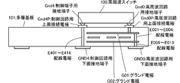
- FIG. 3 is a top view of the high-frequency switch module according to the first embodiment.
- the high frequency switch module 201 is configured by mounting the high frequency switch 100 and the SAW filters F1 to F4 on the upper surface of the multilayer substrate 101.
- the low-pass filters LPF1 and LPF2 shown in FIG. 2 are configured by wiring electrodes inside the multilayer substrate 101 and / or components mounted on the upper surface.
- the multilayer substrate 101 is a ceramic multilayer substrate in which insulators (dielectric ceramics) and wiring electrodes are alternately stacked.
- the high frequency switch 100 is formed on a rectangular plate-like semiconductor substrate.
- the plurality of high-frequency terminals, control terminals, power supply terminals, and ground terminals of the high-frequency switch 100 are formed on one main surface (lower surface) of the semiconductor substrate.
- the multilayer substrate 101 may be formed of a resin such as a liquid crystal polymer.
- upper surface electrodes to which various terminals of the high-frequency switch 100 are connected are formed on the upper surface of the multilayer substrate 101. Further, as shown by a broken line in FIG. 3, a lower surface connection terminal for connecting to an electrode of a circuit board on which the high frequency switch module 201 is mounted is formed on the lower surface of the multilayer substrate 101.
- FIG. 4 is a cross-sectional view showing a connection relationship between the high-frequency switch 100 and the multilayer substrate 101 shown in FIG. However, in order to avoid complication of the drawings, hatching representing a cross-sectional portion is omitted.
- wiring electrodes E401 to E414, E001 to E004, E006 to E013, ground electrodes G01 and G02, and the like are formed in the multilayer substrate 101.
- the other wiring electrodes inside the multilayer substrate 101 are not shown.
- the terminal GND4 is connected via the wiring electrodes E401 to E414.
- the high frequency circuit upper surface connection electrode Gnd0P to which the high frequency circuit ground terminal Gnd0 is connected and the lower surface connection terminal of the multilayer substrate 101 for the high frequency circuit is connected through the wiring electrodes E001 to E004 and E006 to E013.
- the high-frequency circuit upper surface connection electrode Gnd0P is connected to the ground electrodes G01 and G02 in the multilayer substrate 101 via the wiring electrodes E001 to E004 and E006 to E013.
- low-pass filters LPF1 and LPF2 are disposed between the two ground electrodes G01 and G02.
- Each terminal in the high-frequency switch 100 according to the present embodiment is formed by Au bumps or solder bumps, and the high-frequency switch 100 is mounted face-down with its circuit formation surface facing the upper surface side of the multilayer substrate 101.
- FIG. 5 and 6 are diagrams showing the configuration of each layer of the multilayer substrate 101.
- FIG. 5 and 6 are continuous.
- (A) in FIG. 5 is the uppermost layer of the multilayer substrate 101
- (H) in FIG. 6 is the lowermost layer.
- Each figure is the figure which looked at the upper surface direction from the lower surface of each layer. Accordingly, FIG. 5A is a view of the lower surface of the high-frequency switch 100 and the SAW filters F1 to F4 mounted on the upper surface of the multilayer substrate.
- a small circle pattern is a via hole, and the other patterns are a line extending in the surface direction, an electrode for forming an inductor, and an electrode for forming a capacitor.
- the reference numerals in FIGS. 5 and 6 coincide with the reference numerals of the circuit elements shown in FIG. These wiring electrodes form the low-pass filters LPF1 and LPF2 shown in FIG.
- an inductor and a capacitor are formed by a plurality of wiring electrodes, and the low-pass filters LPF1 and LPF2 shown in FIG. 2 are configured by these inductors and capacitors. .
- control circuit ground terminal Gnd4 and the high frequency circuit ground terminal Gnd0 of the high frequency switch 100 are connected to the control circuit lower surface ground terminal GND4 and the high frequency circuit lower surface ground terminal GND0 of the multilayer substrate 101, respectively. Therefore, it is possible to prevent the transmission signal generated in the transmission circuit or the like from entering the control circuit (logic circuit unit) of the high-frequency switch through the ground path.
- the wiring electrodes E401 to E414 that are electrically connected to the upper surface connection electrode to which the control circuit ground terminal Gnd4 is connected are arranged immediately below the control circuit upper surface connection electrode Gnd4P to which the control circuit ground terminal Gnd4 is connected. Furthermore, the control circuit ground terminal Gnd4 is arranged without an unnecessary wiring by arranging the control circuit ground terminal GND4 directly below the control circuit upper surface connection electrode Gnd4P to which the control circuit ground terminal Gnd4 is connected. Since it is connected to the control circuit lower surface ground terminal GND4, it is possible to prevent interference between the ground path of the control circuit of the high-frequency switch and the line for transmitting the transmission / reception signal.
- the low-pass filters LPF1 and LPF2 connected to the transmission signal input terminals Tx1 and Tx2 of the high-frequency switch 100 are disposed between the two ground electrodes G01 and G02 in the multilayer substrate 101, the low-pass filters LPF1 and LPF2 Leakage of the transmission signal from the high frequency switch can be prevented, and interference between the control circuit of the high frequency switch and the transmission circuit can be reduced.
- FIG. 7 is a diagram showing a high frequency switch module according to the second embodiment.
- FIG. 7 shows the configuration of three layers among the layers of the multilayer substrate. What is different from the multilayer substrate shown in FIGS. 5 and 6 in the first embodiment is the shape of the ground electrodes G01 and G02. Other configurations are the same as those of the first embodiment.
- the wiring electrodes (via holes) E405, E414, etc. are arranged at positions not surrounded by the ground electrodes G01, G02 in plan view.
- the wiring electrodes E405 and E414 are electrically connected to the control circuit upper surface connection electrode Gnd4P to which the control circuit ground terminal Gnd4 is connected.
- the ground electrodes G01 and G02 are formed such that the formation region of the ground electrodes G01 and G02 does not surround the formation positions of the wiring electrodes (via holes) E405 and E414 that are electrically connected to the control circuit upper surface connection electrode Gnd4P in a plan view.
- the ground electrodes G01 and G02 are arranged at positions that do not overlap with the control circuit lower surface ground terminal GND4 in plan view.
- the control circuit lower surface ground terminal and the high frequency circuit lower surface ground terminal may be arranged along different sides of the multilayer substrate. As a result, the capacitance generated between the control circuit lower surface ground terminal and the high frequency circuit lower surface ground terminal can be reduced to further prevent the high frequency signal and noise from wrapping around.
- control terminal ground terminal GND4 may be provided at a position away from (not adjacent to) a terminal where power is applied, such as a UMTS terminal, a transmission signal input terminal, or an antenna terminal. As a result, the wraparound of the high-frequency signal to the control circuit in the high-frequency switch can be further reduced.
Landscapes
- Engineering & Computer Science (AREA)
- Computer Networks & Wireless Communication (AREA)
- Signal Processing (AREA)
- Transceivers (AREA)
Priority Applications (4)
| Application Number | Priority Date | Filing Date | Title |
|---|---|---|---|
| CN201080026188.7A CN102460985B (zh) | 2009-06-11 | 2010-04-19 | 高频开关模块 |
| JP2011518354A JP5152409B2 (ja) | 2009-06-11 | 2010-04-19 | 高周波スイッチモジュール |
| DE112010001927.4T DE112010001927B4 (de) | 2009-06-11 | 2010-04-19 | Hochfrequenzschaltermodul |
| US13/314,339 US8253483B2 (en) | 2009-06-11 | 2011-12-08 | High-frequency switch module |
Applications Claiming Priority (2)
| Application Number | Priority Date | Filing Date | Title |
|---|---|---|---|
| JP2009140047 | 2009-06-11 | ||
| JP2009-140047 | 2009-06-11 |
Related Child Applications (1)
| Application Number | Title | Priority Date | Filing Date |
|---|---|---|---|
| US13/314,339 Continuation US8253483B2 (en) | 2009-06-11 | 2011-12-08 | High-frequency switch module |
Publications (1)
| Publication Number | Publication Date |
|---|---|
| WO2010143472A1 true WO2010143472A1 (ja) | 2010-12-16 |
Family
ID=43308732
Family Applications (1)
| Application Number | Title | Priority Date | Filing Date |
|---|---|---|---|
| PCT/JP2010/056906 WO2010143472A1 (ja) | 2009-06-11 | 2010-04-19 | 高周波スイッチモジュール |
Country Status (5)
| Country | Link |
|---|---|
| US (1) | US8253483B2 (zh) |
| JP (1) | JP5152409B2 (zh) |
| CN (1) | CN102460985B (zh) |
| DE (1) | DE112010001927B4 (zh) |
| WO (1) | WO2010143472A1 (zh) |
Cited By (3)
| Publication number | Priority date | Publication date | Assignee | Title |
|---|---|---|---|---|
| WO2013031602A1 (ja) * | 2011-09-02 | 2013-03-07 | 株式会社村田製作所 | 回路モジュール及び複合回路モジュール |
| CN103416001A (zh) * | 2011-03-02 | 2013-11-27 | 株式会社村田制作所 | 高频模块 |
| WO2018123698A1 (ja) * | 2016-12-27 | 2018-07-05 | 株式会社村田製作所 | 高周波モジュールおよび通信装置 |
Families Citing this family (14)
| Publication number | Priority date | Publication date | Assignee | Title |
|---|---|---|---|---|
| JP5610111B1 (ja) * | 2012-12-07 | 2014-10-22 | 株式会社村田製作所 | 高周波モジュール |
| JP5773096B1 (ja) * | 2013-10-17 | 2015-09-02 | 株式会社村田製作所 | 高周波回路モジュール |
| JP6443263B2 (ja) * | 2015-08-10 | 2018-12-26 | 株式会社村田製作所 | 高周波モジュール |
| JP6451605B2 (ja) * | 2015-11-18 | 2019-01-16 | 株式会社村田製作所 | 高周波モジュール及び通信装置 |
| JP6685414B2 (ja) * | 2016-09-23 | 2020-04-22 | 三菱電機株式会社 | 電力用半導体モジュール及び電力用半導体装置 |
| WO2018088410A1 (ja) * | 2016-11-11 | 2018-05-17 | 株式会社村田製作所 | スイッチic、高周波モジュールおよび通信装置 |
| JP6729790B2 (ja) * | 2017-03-14 | 2020-07-22 | 株式会社村田製作所 | 高周波モジュール |
| KR102536264B1 (ko) * | 2018-01-26 | 2023-05-25 | 삼성전자주식회사 | 안테나 성능 저하를 방지하기 위한 기판 및 이를 포함하는 전자 장치 |
| WO2021002157A1 (ja) * | 2019-07-03 | 2021-01-07 | 株式会社村田製作所 | 高周波モジュール及び通信装置 |
| WO2021006020A1 (ja) * | 2019-07-09 | 2021-01-14 | 株式会社村田製作所 | 高周波モジュール及び通信装置 |
| JP2021103713A (ja) * | 2019-12-25 | 2021-07-15 | 株式会社村田製作所 | 高周波モジュール及び通信装置 |
| JP2021145282A (ja) * | 2020-03-13 | 2021-09-24 | 株式会社村田製作所 | 高周波モジュールおよび通信装置 |
| JP2021158554A (ja) * | 2020-03-27 | 2021-10-07 | 株式会社村田製作所 | 高周波モジュールおよび通信装置 |
| JP2021158556A (ja) * | 2020-03-27 | 2021-10-07 | 株式会社村田製作所 | 高周波モジュールおよび通信装置 |
Citations (2)
| Publication number | Priority date | Publication date | Assignee | Title |
|---|---|---|---|---|
| JP2006073673A (ja) * | 2004-08-31 | 2006-03-16 | Kyocera Corp | 高周波モジュール及び無線通信装置 |
| JP2006211144A (ja) * | 2005-01-26 | 2006-08-10 | Kyocera Corp | 高周波モジュール及び無線通信機器 |
Family Cites Families (11)
| Publication number | Priority date | Publication date | Assignee | Title |
|---|---|---|---|---|
| JPS63122306A (ja) | 1986-11-12 | 1988-05-26 | Omron Tateisi Electronics Co | 集積回路の接地回路 |
| JPH08204344A (ja) | 1995-01-23 | 1996-08-09 | Sony Corp | 多層配線基板 |
| JP2003087149A (ja) * | 2001-09-14 | 2003-03-20 | Matsushita Electric Ind Co Ltd | 高周波複合スイッチモジュール |
| CN1266971C (zh) * | 2002-10-23 | 2006-07-26 | 株式会社村田制作所 | 高频组件及通信装置 |
| JP3936949B2 (ja) * | 2004-10-25 | 2007-06-27 | 株式会社日立国際電気 | 高周波スイッチ回路装置 |
| JP4527570B2 (ja) | 2005-03-08 | 2010-08-18 | 京セラ株式会社 | 高周波モジュ−ル及びそれを搭載した無線通信装置 |
| WO2007018037A1 (ja) * | 2005-08-09 | 2007-02-15 | Hitachi Metals, Ltd. | 高周波スイッチ回路 |
| JP2007129514A (ja) | 2005-11-04 | 2007-05-24 | Hitachi Metals Ltd | 高周波スイッチモジュール、およびこれを用いた通信装置 |
| JP5029946B2 (ja) | 2007-04-24 | 2012-09-19 | 日立金属株式会社 | スイッチモジュール |
| TW200924276A (en) * | 2007-11-28 | 2009-06-01 | Murata Manufacturing Co | Low-voltage control high-frequency switch and composite high frequency component |
| JP5625453B2 (ja) * | 2009-05-26 | 2014-11-19 | 株式会社村田製作所 | 高周波スイッチモジュール |
-
2010
- 2010-04-19 WO PCT/JP2010/056906 patent/WO2010143472A1/ja active Application Filing
- 2010-04-19 CN CN201080026188.7A patent/CN102460985B/zh active Active
- 2010-04-19 DE DE112010001927.4T patent/DE112010001927B4/de not_active Expired - Fee Related
- 2010-04-19 JP JP2011518354A patent/JP5152409B2/ja active Active
-
2011
- 2011-12-08 US US13/314,339 patent/US8253483B2/en active Active
Patent Citations (2)
| Publication number | Priority date | Publication date | Assignee | Title |
|---|---|---|---|---|
| JP2006073673A (ja) * | 2004-08-31 | 2006-03-16 | Kyocera Corp | 高周波モジュール及び無線通信装置 |
| JP2006211144A (ja) * | 2005-01-26 | 2006-08-10 | Kyocera Corp | 高周波モジュール及び無線通信機器 |
Cited By (8)
| Publication number | Priority date | Publication date | Assignee | Title |
|---|---|---|---|---|
| CN103416001A (zh) * | 2011-03-02 | 2013-11-27 | 株式会社村田制作所 | 高频模块 |
| CN103416001B (zh) * | 2011-03-02 | 2015-05-20 | 株式会社村田制作所 | 高频模块 |
| US9319092B2 (en) | 2011-03-02 | 2016-04-19 | Murata Manufacturing Co., Ltd. | High-frequency module |
| WO2013031602A1 (ja) * | 2011-09-02 | 2013-03-07 | 株式会社村田製作所 | 回路モジュール及び複合回路モジュール |
| JPWO2013031602A1 (ja) * | 2011-09-02 | 2015-03-23 | 株式会社村田製作所 | 回路モジュール及び複合回路モジュール |
| US9548440B2 (en) | 2011-09-02 | 2017-01-17 | Murata Manufacturing Co., Ltd. | Circuit module and composite circuit module |
| WO2018123698A1 (ja) * | 2016-12-27 | 2018-07-05 | 株式会社村田製作所 | 高周波モジュールおよび通信装置 |
| US10873352B2 (en) | 2016-12-27 | 2020-12-22 | Murata Manufacturing Co., Ltd. | Radio-frequency module and communication apparatus |
Also Published As
| Publication number | Publication date |
|---|---|
| JP5152409B2 (ja) | 2013-02-27 |
| CN102460985A (zh) | 2012-05-16 |
| DE112010001927B4 (de) | 2018-02-22 |
| US8253483B2 (en) | 2012-08-28 |
| US20120075002A1 (en) | 2012-03-29 |
| JPWO2010143472A1 (ja) | 2012-11-22 |
| DE112010001927T5 (de) | 2012-11-08 |
| CN102460985B (zh) | 2014-05-14 |
Similar Documents
| Publication | Publication Date | Title |
|---|---|---|
| JP5152409B2 (ja) | 高周波スイッチモジュール | |
| JP5677499B2 (ja) | 高周波回路モジュール | |
| US11476226B2 (en) | Radio-frequency module and communication device | |
| US9451690B2 (en) | High frequency circuit module | |
| JP4715973B2 (ja) | 高周波スイッチモジュール | |
| JP2016096439A (ja) | 弾性波デバイス、送受信デバイスおよび移動体通信機 | |
| US9413413B2 (en) | High-frequency module | |
| US20130141180A1 (en) | High-frequency module | |
| WO2022107460A1 (ja) | 高周波モジュールおよび通信装置 | |
| WO2010143471A1 (ja) | 高周波スイッチモジュール | |
| US8912866B2 (en) | Dual-band surface acoustic wave filter and composite high-frequency component | |
| US8422972B2 (en) | Antenna combining module | |
| JP4378703B2 (ja) | 高周波回路部品 | |
| JP5660223B2 (ja) | 分波装置 | |
| JPWO2013047357A1 (ja) | 高周波モジュール、送信フィルタモジュール、受信フィルタモジュール | |
| JPWO2009157283A1 (ja) | 高周波モジュール | |
| US20230262879A1 (en) | High-frequency module and communication device | |
| WO2022138441A1 (ja) | 高周波モジュール及び通信装置 | |
| US20230328939A1 (en) | Radio frequency module and communication device |
Legal Events
| Date | Code | Title | Description |
|---|---|---|---|
| WWE | Wipo information: entry into national phase |
Ref document number: 201080026188.7 Country of ref document: CN |
|
| 121 | Ep: the epo has been informed by wipo that ep was designated in this application |
Ref document number: 10786003 Country of ref document: EP Kind code of ref document: A1 |
|
| ENP | Entry into the national phase |
Ref document number: 2011518354 Country of ref document: JP Kind code of ref document: A |
|
| WWE | Wipo information: entry into national phase |
Ref document number: 112010001927 Country of ref document: DE Ref document number: 1120100019274 Country of ref document: DE |
|
| 122 | Ep: pct application non-entry in european phase |
Ref document number: 10786003 Country of ref document: EP Kind code of ref document: A1 |