WO2010137099A1 - 太陽電池バックシート用フィルム、それを用いた太陽電池バックシート、および太陽電池 - Google Patents
太陽電池バックシート用フィルム、それを用いた太陽電池バックシート、および太陽電池 Download PDFInfo
- Publication number
- WO2010137099A1 WO2010137099A1 PCT/JP2009/059495 JP2009059495W WO2010137099A1 WO 2010137099 A1 WO2010137099 A1 WO 2010137099A1 JP 2009059495 W JP2009059495 W JP 2009059495W WO 2010137099 A1 WO2010137099 A1 WO 2010137099A1
- Authority
- WO
- WIPO (PCT)
- Prior art keywords
- layer
- film
- partial discharge
- solar cell
- discharge voltage
- Prior art date
Links
- 229920000728 polyester Polymers 0.000 claims abstract description 41
- 229920005989 resin Polymers 0.000 claims description 126
- 239000011347 resin Substances 0.000 claims description 126
- 239000004020 conductor Substances 0.000 claims description 106
- 239000000463 material Substances 0.000 claims description 87
- -1 oxazoline compound Chemical class 0.000 claims description 82
- 150000001875 compounds Chemical class 0.000 claims description 36
- 230000008018 melting Effects 0.000 claims description 32
- 238000002844 melting Methods 0.000 claims description 32
- 239000003431 cross linking reagent Substances 0.000 claims description 30
- 238000010248 power generation Methods 0.000 claims description 24
- IJGRMHOSHXDMSA-UHFFFAOYSA-N Atomic nitrogen Chemical compound N#N IJGRMHOSHXDMSA-UHFFFAOYSA-N 0.000 claims description 23
- 239000004611 light stabiliser Substances 0.000 claims description 13
- 239000006172 buffering agent Substances 0.000 claims description 12
- 125000003178 carboxy group Chemical group [H]OC(*)=O 0.000 claims description 8
- 229910052757 nitrogen Inorganic materials 0.000 claims description 8
- 125000002091 cationic group Chemical group 0.000 claims description 7
- NIXOWILDQLNWCW-UHFFFAOYSA-N acrylic acid group Chemical group C(C=C)(=O)O NIXOWILDQLNWCW-UHFFFAOYSA-N 0.000 claims description 6
- 238000000113 differential scanning calorimetry Methods 0.000 claims description 6
- 239000010410 layer Substances 0.000 description 562
- 239000010408 film Substances 0.000 description 322
- 208000028659 discharge Diseases 0.000 description 301
- VZSRBBMJRBPUNF-UHFFFAOYSA-N 2-(2,3-dihydro-1H-inden-2-ylamino)-N-[3-oxo-3-(2,4,6,7-tetrahydrotriazolo[4,5-c]pyridin-5-yl)propyl]pyrimidine-5-carboxamide Chemical compound C1C(CC2=CC=CC=C12)NC1=NC=C(C=N1)C(=O)NCCC(N1CC2=C(CC1)NN=N2)=O VZSRBBMJRBPUNF-UHFFFAOYSA-N 0.000 description 129
- 238000000034 method Methods 0.000 description 110
- 238000010438 heat treatment Methods 0.000 description 84
- 239000011248 coating agent Substances 0.000 description 58
- 239000002585 base Substances 0.000 description 44
- 229920000139 polyethylene terephthalate Polymers 0.000 description 44
- 239000005020 polyethylene terephthalate Substances 0.000 description 44
- 230000008602 contraction Effects 0.000 description 37
- 238000000576 coating method Methods 0.000 description 36
- 238000006116 polymerization reaction Methods 0.000 description 34
- 238000005259 measurement Methods 0.000 description 33
- XLYOFNOQVPJJNP-UHFFFAOYSA-N water Substances O XLYOFNOQVPJJNP-UHFFFAOYSA-N 0.000 description 30
- 239000000203 mixture Substances 0.000 description 28
- LYCAIKOWRPUZTN-UHFFFAOYSA-N Ethylene glycol Chemical compound OCCO LYCAIKOWRPUZTN-UHFFFAOYSA-N 0.000 description 27
- GWEVSGVZZGPLCZ-UHFFFAOYSA-N Titan oxide Chemical compound O=[Ti]=O GWEVSGVZZGPLCZ-UHFFFAOYSA-N 0.000 description 25
- 239000007789 gas Substances 0.000 description 25
- 229920001225 polyester resin Polymers 0.000 description 25
- 239000004645 polyester resin Substances 0.000 description 24
- OGIDPMRJRNCKJF-UHFFFAOYSA-N titanium oxide Inorganic materials [Ti]=O OGIDPMRJRNCKJF-UHFFFAOYSA-N 0.000 description 24
- 125000001905 inorganic group Chemical group 0.000 description 23
- 239000002994 raw material Substances 0.000 description 23
- XLOMVQKBTHCTTD-UHFFFAOYSA-N Zinc monoxide Chemical compound [Zn]=O XLOMVQKBTHCTTD-UHFFFAOYSA-N 0.000 description 20
- 230000009257 reactivity Effects 0.000 description 20
- 239000000243 solution Substances 0.000 description 20
- 230000001965 increasing effect Effects 0.000 description 19
- 230000014759 maintenance of location Effects 0.000 description 19
- 239000004094 surface-active agent Substances 0.000 description 19
- 230000007423 decrease Effects 0.000 description 17
- 239000010419 fine particle Substances 0.000 description 17
- 239000011230 binding agent Substances 0.000 description 16
- 239000002245 particle Substances 0.000 description 16
- 238000006068 polycondensation reaction Methods 0.000 description 16
- 239000000523 sample Substances 0.000 description 16
- 239000005038 ethylene vinyl acetate Substances 0.000 description 15
- 238000001125 extrusion Methods 0.000 description 15
- 238000006460 hydrolysis reaction Methods 0.000 description 15
- 238000002156 mixing Methods 0.000 description 15
- 229920001200 poly(ethylene-vinyl acetate) Polymers 0.000 description 15
- 239000007790 solid phase Substances 0.000 description 15
- 239000000758 substrate Substances 0.000 description 15
- OKTJSMMVPCPJKN-UHFFFAOYSA-N Carbon Chemical compound [C] OKTJSMMVPCPJKN-UHFFFAOYSA-N 0.000 description 13
- 239000006096 absorbing agent Substances 0.000 description 13
- 239000003795 chemical substances by application Substances 0.000 description 13
- 230000007774 longterm Effects 0.000 description 13
- 239000011159 matrix material Substances 0.000 description 13
- 239000006097 ultraviolet radiation absorber Substances 0.000 description 13
- 238000006243 chemical reaction Methods 0.000 description 12
- 230000000694 effects Effects 0.000 description 12
- 238000004519 manufacturing process Methods 0.000 description 12
- 229910052751 metal Inorganic materials 0.000 description 12
- 239000002184 metal Substances 0.000 description 12
- 229920000178 Acrylic resin Polymers 0.000 description 11
- 239000004925 Acrylic resin Substances 0.000 description 11
- PXHVJJICTQNCMI-UHFFFAOYSA-N Nickel Chemical compound [Ni] PXHVJJICTQNCMI-UHFFFAOYSA-N 0.000 description 11
- RTAQQCXQSZGOHL-UHFFFAOYSA-N Titanium Chemical compound [Ti] RTAQQCXQSZGOHL-UHFFFAOYSA-N 0.000 description 11
- 230000007062 hydrolysis Effects 0.000 description 11
- 239000000178 monomer Substances 0.000 description 11
- 239000002904 solvent Substances 0.000 description 11
- 239000000126 substance Substances 0.000 description 11
- 229920005992 thermoplastic resin Polymers 0.000 description 11
- XEEYBQQBJWHFJM-UHFFFAOYSA-N Iron Chemical compound [Fe] XEEYBQQBJWHFJM-UHFFFAOYSA-N 0.000 description 10
- NBIIXXVUZAFLBC-UHFFFAOYSA-N Phosphoric acid Chemical compound OP(O)(O)=O NBIIXXVUZAFLBC-UHFFFAOYSA-N 0.000 description 10
- 230000004888 barrier function Effects 0.000 description 10
- 239000003054 catalyst Substances 0.000 description 10
- 239000007787 solid Substances 0.000 description 10
- 239000011787 zinc oxide Substances 0.000 description 10
- OKKJLVBELUTLKV-UHFFFAOYSA-N Methanol Chemical compound OC OKKJLVBELUTLKV-UHFFFAOYSA-N 0.000 description 9
- 238000011088 calibration curve Methods 0.000 description 9
- 239000002131 composite material Substances 0.000 description 9
- 230000006866 deterioration Effects 0.000 description 9
- 230000005684 electric field Effects 0.000 description 9
- 230000006870 function Effects 0.000 description 9
- 125000000524 functional group Chemical group 0.000 description 9
- 150000002291 germanium compounds Chemical class 0.000 description 9
- 229910052783 alkali metal Inorganic materials 0.000 description 8
- 229910052782 aluminium Inorganic materials 0.000 description 8
- XAGFODPZIPBFFR-UHFFFAOYSA-N aluminium Chemical compound [Al] XAGFODPZIPBFFR-UHFFFAOYSA-N 0.000 description 8
- ADCOVFLJGNWWNZ-UHFFFAOYSA-N antimony trioxide Chemical compound O=[Sb]O[Sb]=O ADCOVFLJGNWWNZ-UHFFFAOYSA-N 0.000 description 8
- 230000015572 biosynthetic process Effects 0.000 description 8
- 239000000872 buffer Substances 0.000 description 8
- 150000001718 carbodiimides Chemical class 0.000 description 8
- 229910052799 carbon Inorganic materials 0.000 description 8
- 230000000052 comparative effect Effects 0.000 description 8
- 238000005227 gel permeation chromatography Methods 0.000 description 8
- 238000010030 laminating Methods 0.000 description 8
- 229920006122 polyamide resin Polymers 0.000 description 8
- 238000007789 sealing Methods 0.000 description 8
- 229910052719 titanium Inorganic materials 0.000 description 8
- 239000010936 titanium Substances 0.000 description 8
- HMUNWXXNJPVALC-UHFFFAOYSA-N 1-[4-[2-(2,3-dihydro-1H-inden-2-ylamino)pyrimidin-5-yl]piperazin-1-yl]-2-(2,4,6,7-tetrahydrotriazolo[4,5-c]pyridin-5-yl)ethanone Chemical compound C1C(CC2=CC=CC=C12)NC1=NC=C(C=N1)N1CCN(CC1)C(CN1CC2=C(CC1)NN=N2)=O HMUNWXXNJPVALC-UHFFFAOYSA-N 0.000 description 7
- MYMOFIZGZYHOMD-UHFFFAOYSA-N Dioxygen Chemical compound O=O MYMOFIZGZYHOMD-UHFFFAOYSA-N 0.000 description 7
- 229920001940 conductive polymer Polymers 0.000 description 7
- 229910001873 dinitrogen Inorganic materials 0.000 description 7
- 229910001882 dioxygen Inorganic materials 0.000 description 7
- 239000006185 dispersion Substances 0.000 description 7
- 238000010828 elution Methods 0.000 description 7
- 150000002148 esters Chemical class 0.000 description 7
- 229920005672 polyolefin resin Polymers 0.000 description 7
- 238000012545 processing Methods 0.000 description 7
- 238000012360 testing method Methods 0.000 description 7
- 238000007740 vapor deposition Methods 0.000 description 7
- OFOBLEOULBTSOW-UHFFFAOYSA-N Malonic acid Chemical compound OC(=O)CC(O)=O OFOBLEOULBTSOW-UHFFFAOYSA-N 0.000 description 6
- 229920002614 Polyether block amide Polymers 0.000 description 6
- 239000004721 Polyphenylene oxide Substances 0.000 description 6
- 239000002253 acid Substances 0.000 description 6
- 239000000853 adhesive Substances 0.000 description 6
- 230000001070 adhesive effect Effects 0.000 description 6
- 150000001463 antimony compounds Chemical class 0.000 description 6
- 239000012298 atmosphere Substances 0.000 description 6
- KRKNYBCHXYNGOX-UHFFFAOYSA-N citric acid Chemical compound OC(=O)CC(O)(C(O)=O)CC(O)=O KRKNYBCHXYNGOX-UHFFFAOYSA-N 0.000 description 6
- 239000011888 foil Substances 0.000 description 6
- 229910052809 inorganic oxide Inorganic materials 0.000 description 6
- 238000004898 kneading Methods 0.000 description 6
- 239000012299 nitrogen atmosphere Substances 0.000 description 6
- 229920006267 polyester film Polymers 0.000 description 6
- 229920000570 polyether Polymers 0.000 description 6
- 238000004544 sputter deposition Methods 0.000 description 6
- 150000003609 titanium compounds Chemical class 0.000 description 6
- 238000005809 transesterification reaction Methods 0.000 description 6
- 238000009281 ultraviolet germicidal irradiation Methods 0.000 description 6
- 239000004593 Epoxy Chemical class 0.000 description 5
- ZLMJMSJWJFRBEC-UHFFFAOYSA-N Potassium Chemical compound [K] ZLMJMSJWJFRBEC-UHFFFAOYSA-N 0.000 description 5
- 229910000147 aluminium phosphate Inorganic materials 0.000 description 5
- QVGXLLKOCUKJST-UHFFFAOYSA-N atomic oxygen Chemical compound [O] QVGXLLKOCUKJST-UHFFFAOYSA-N 0.000 description 5
- IISBACLAFKSPIT-UHFFFAOYSA-N bisphenol A Chemical compound C=1C=C(O)C=CC=1C(C)(C)C1=CC=C(O)C=C1 IISBACLAFKSPIT-UHFFFAOYSA-N 0.000 description 5
- 230000000903 blocking effect Effects 0.000 description 5
- 229910021393 carbon nanotube Inorganic materials 0.000 description 5
- 239000002041 carbon nanotube Substances 0.000 description 5
- 238000003851 corona treatment Methods 0.000 description 5
- 239000013078 crystal Substances 0.000 description 5
- 238000005520 cutting process Methods 0.000 description 5
- 238000000354 decomposition reaction Methods 0.000 description 5
- 150000002009 diols Chemical class 0.000 description 5
- 229910001502 inorganic halide Inorganic materials 0.000 description 5
- 229910052945 inorganic sulfide Inorganic materials 0.000 description 5
- 150000004767 nitrides Chemical class 0.000 description 5
- 239000001301 oxygen Substances 0.000 description 5
- 229910052760 oxygen Inorganic materials 0.000 description 5
- 239000002861 polymer material Substances 0.000 description 5
- 230000008569 process Effects 0.000 description 5
- 238000001291 vacuum drying Methods 0.000 description 5
- XMWRBQBLMFGWIX-UHFFFAOYSA-N C60 fullerene Chemical compound C12=C3C(C4=C56)=C7C8=C5C5=C9C%10=C6C6=C4C1=C1C4=C6C6=C%10C%10=C9C9=C%11C5=C8C5=C8C7=C3C3=C7C2=C1C1=C2C4=C6C4=C%10C6=C9C9=C%11C5=C5C8=C3C3=C7C1=C1C2=C4C6=C2C9=C5C3=C12 XMWRBQBLMFGWIX-UHFFFAOYSA-N 0.000 description 4
- KDLHZDBZIXYQEI-UHFFFAOYSA-N Palladium Chemical compound [Pd] KDLHZDBZIXYQEI-UHFFFAOYSA-N 0.000 description 4
- CDBYLPFSWZWCQE-UHFFFAOYSA-L Sodium Carbonate Chemical compound [Na+].[Na+].[O-]C([O-])=O CDBYLPFSWZWCQE-UHFFFAOYSA-L 0.000 description 4
- KKEYFWRCBNTPAC-UHFFFAOYSA-N Terephthalic acid Chemical compound OC(=O)C1=CC=C(C(O)=O)C=C1 KKEYFWRCBNTPAC-UHFFFAOYSA-N 0.000 description 4
- HCHKCACWOHOZIP-UHFFFAOYSA-N Zinc Chemical compound [Zn] HCHKCACWOHOZIP-UHFFFAOYSA-N 0.000 description 4
- 238000010521 absorption reaction Methods 0.000 description 4
- 239000000654 additive Substances 0.000 description 4
- 150000001340 alkali metals Chemical class 0.000 description 4
- PNEYBMLMFCGWSK-UHFFFAOYSA-N aluminium oxide Inorganic materials [O-2].[O-2].[O-2].[Al+3].[Al+3] PNEYBMLMFCGWSK-UHFFFAOYSA-N 0.000 description 4
- TZCXTZWJZNENPQ-UHFFFAOYSA-L barium sulfate Chemical compound [Ba+2].[O-]S([O-])(=O)=O TZCXTZWJZNENPQ-UHFFFAOYSA-L 0.000 description 4
- QHIWVLPBUQWDMQ-UHFFFAOYSA-N butyl prop-2-enoate;methyl 2-methylprop-2-enoate;prop-2-enoic acid Chemical compound OC(=O)C=C.COC(=O)C(C)=C.CCCCOC(=O)C=C QHIWVLPBUQWDMQ-UHFFFAOYSA-N 0.000 description 4
- 150000001732 carboxylic acid derivatives Chemical class 0.000 description 4
- 230000015556 catabolic process Effects 0.000 description 4
- 238000001816 cooling Methods 0.000 description 4
- 229920001577 copolymer Polymers 0.000 description 4
- 150000001925 cycloalkenes Chemical class 0.000 description 4
- WOZVHXUHUFLZGK-UHFFFAOYSA-N dimethyl terephthalate Chemical compound COC(=O)C1=CC=C(C(=O)OC)C=C1 WOZVHXUHUFLZGK-UHFFFAOYSA-N 0.000 description 4
- 238000005886 esterification reaction Methods 0.000 description 4
- 229920005648 ethylene methacrylic acid copolymer Polymers 0.000 description 4
- 229920006244 ethylene-ethyl acrylate Polymers 0.000 description 4
- 229920006225 ethylene-methyl acrylate Polymers 0.000 description 4
- 229910003472 fullerene Inorganic materials 0.000 description 4
- 229910052736 halogen Inorganic materials 0.000 description 4
- 150000002367 halogens Chemical class 0.000 description 4
- 230000006872 improvement Effects 0.000 description 4
- 229910010272 inorganic material Inorganic materials 0.000 description 4
- 239000011147 inorganic material Substances 0.000 description 4
- QQVIHTHCMHWDBS-UHFFFAOYSA-N isophthalic acid Chemical compound OC(=O)C1=CC=CC(C(O)=O)=C1 QQVIHTHCMHWDBS-UHFFFAOYSA-N 0.000 description 4
- JVTAAEKCZFNVCJ-UHFFFAOYSA-N lactic acid Chemical compound CC(O)C(O)=O JVTAAEKCZFNVCJ-UHFFFAOYSA-N 0.000 description 4
- MRELNEQAGSRDBK-UHFFFAOYSA-N lanthanum(3+);oxygen(2-) Chemical compound [O-2].[O-2].[O-2].[La+3].[La+3] MRELNEQAGSRDBK-UHFFFAOYSA-N 0.000 description 4
- 239000011368 organic material Substances 0.000 description 4
- TWNQGVIAIRXVLR-UHFFFAOYSA-N oxo(oxoalumanyloxy)alumane Chemical compound O=[Al]O[Al]=O TWNQGVIAIRXVLR-UHFFFAOYSA-N 0.000 description 4
- XNGIFLGASWRNHJ-UHFFFAOYSA-N phthalic acid Chemical compound OC(=O)C1=CC=CC=C1C(O)=O XNGIFLGASWRNHJ-UHFFFAOYSA-N 0.000 description 4
- BASFCYQUMIYNBI-UHFFFAOYSA-N platinum Chemical compound [Pt] BASFCYQUMIYNBI-UHFFFAOYSA-N 0.000 description 4
- 229910052700 potassium Inorganic materials 0.000 description 4
- 239000011591 potassium Substances 0.000 description 4
- 230000002040 relaxant effect Effects 0.000 description 4
- YGSDEFSMJLZEOE-UHFFFAOYSA-N salicylic acid Chemical compound OC(=O)C1=CC=CC=C1O YGSDEFSMJLZEOE-UHFFFAOYSA-N 0.000 description 4
- 239000002356 single layer Substances 0.000 description 4
- 239000003643 water by type Substances 0.000 description 4
- 229910052725 zinc Inorganic materials 0.000 description 4
- 239000011701 zinc Substances 0.000 description 4
- IMSODMZESSGVBE-UHFFFAOYSA-N 2-Oxazoline Chemical compound C1CN=CO1 IMSODMZESSGVBE-UHFFFAOYSA-N 0.000 description 3
- LLLVZDVNHNWSDS-UHFFFAOYSA-N 4-methylidene-3,5-dioxabicyclo[5.2.2]undeca-1(9),7,10-triene-2,6-dione Chemical compound C1(C2=CC=C(C(=O)OC(=C)O1)C=C2)=O LLLVZDVNHNWSDS-UHFFFAOYSA-N 0.000 description 3
- UHOVQNZJYSORNB-UHFFFAOYSA-N Benzene Chemical compound C1=CC=CC=C1 UHOVQNZJYSORNB-UHFFFAOYSA-N 0.000 description 3
- 229920000049 Carbon (fiber) Polymers 0.000 description 3
- YCKRFDGAMUMZLT-UHFFFAOYSA-N Fluorine atom Chemical compound [F] YCKRFDGAMUMZLT-UHFFFAOYSA-N 0.000 description 3
- DGAQECJNVWCQMB-PUAWFVPOSA-M Ilexoside XXIX Chemical compound C[C@@H]1CC[C@@]2(CC[C@@]3(C(=CC[C@H]4[C@]3(CC[C@@H]5[C@@]4(CC[C@@H](C5(C)C)OS(=O)(=O)[O-])C)C)[C@@H]2[C@]1(C)O)C)C(=O)O[C@H]6[C@@H]([C@H]([C@@H]([C@H](O6)CO)O)O)O.[Na+] DGAQECJNVWCQMB-PUAWFVPOSA-M 0.000 description 3
- 229920000877 Melamine resin Chemical class 0.000 description 3
- VCUFZILGIRCDQQ-KRWDZBQOSA-N N-[[(5S)-2-oxo-3-(2-oxo-3H-1,3-benzoxazol-6-yl)-1,3-oxazolidin-5-yl]methyl]-2-[[3-(trifluoromethoxy)phenyl]methylamino]pyrimidine-5-carboxamide Chemical compound O=C1O[C@H](CN1C1=CC2=C(NC(O2)=O)C=C1)CNC(=O)C=1C=NC(=NC=1)NCC1=CC(=CC=C1)OC(F)(F)F VCUFZILGIRCDQQ-KRWDZBQOSA-N 0.000 description 3
- 239000002033 PVDF binder Substances 0.000 description 3
- 239000004698 Polyethylene Substances 0.000 description 3
- 239000004743 Polypropylene Substances 0.000 description 3
- 239000004793 Polystyrene Substances 0.000 description 3
- VYPSYNLAJGMNEJ-UHFFFAOYSA-N Silicium dioxide Chemical compound O=[Si]=O VYPSYNLAJGMNEJ-UHFFFAOYSA-N 0.000 description 3
- XUIMIQQOPSSXEZ-UHFFFAOYSA-N Silicon Chemical compound [Si] XUIMIQQOPSSXEZ-UHFFFAOYSA-N 0.000 description 3
- NINIDFKCEFEMDL-UHFFFAOYSA-N Sulfur Chemical compound [S] NINIDFKCEFEMDL-UHFFFAOYSA-N 0.000 description 3
- 239000012790 adhesive layer Substances 0.000 description 3
- 150000001412 amines Chemical class 0.000 description 3
- 229910052787 antimony Inorganic materials 0.000 description 3
- WATWJIUSRGPENY-UHFFFAOYSA-N antimony atom Chemical compound [Sb] WATWJIUSRGPENY-UHFFFAOYSA-N 0.000 description 3
- QRUDEWIWKLJBPS-UHFFFAOYSA-N benzotriazole Chemical compound C1=CC=C2N[N][N]C2=C1 QRUDEWIWKLJBPS-UHFFFAOYSA-N 0.000 description 3
- 239000012964 benzotriazole Substances 0.000 description 3
- 239000004917 carbon fiber Substances 0.000 description 3
- 238000004132 cross linking Methods 0.000 description 3
- 238000006731 degradation reaction Methods 0.000 description 3
- 238000000151 deposition Methods 0.000 description 3
- 238000013461 design Methods 0.000 description 3
- MTHSVFCYNBDYFN-UHFFFAOYSA-N diethylene glycol Chemical compound OCCOCCO MTHSVFCYNBDYFN-UHFFFAOYSA-N 0.000 description 3
- 238000001035 drying Methods 0.000 description 3
- 230000005611 electricity Effects 0.000 description 3
- 238000010894 electron beam technology Methods 0.000 description 3
- 238000000605 extraction Methods 0.000 description 3
- 239000000945 filler Substances 0.000 description 3
- 239000011737 fluorine Substances 0.000 description 3
- 229910052731 fluorine Inorganic materials 0.000 description 3
- 239000011521 glass Substances 0.000 description 3
- 125000003055 glycidyl group Chemical group C(C1CO1)* 0.000 description 3
- 229910052742 iron Inorganic materials 0.000 description 3
- WABPQHHGFIMREM-UHFFFAOYSA-N lead(0) Chemical compound [Pb] WABPQHHGFIMREM-UHFFFAOYSA-N 0.000 description 3
- UEGPKNKPLBYCNK-UHFFFAOYSA-L magnesium acetate Chemical compound [Mg+2].CC([O-])=O.CC([O-])=O UEGPKNKPLBYCNK-UHFFFAOYSA-L 0.000 description 3
- 239000011654 magnesium acetate Substances 0.000 description 3
- 235000011285 magnesium acetate Nutrition 0.000 description 3
- 229940069446 magnesium acetate Drugs 0.000 description 3
- 239000011572 manganese Substances 0.000 description 3
- 229910044991 metal oxide Inorganic materials 0.000 description 3
- 150000004706 metal oxides Chemical class 0.000 description 3
- VNWKTOKETHGBQD-UHFFFAOYSA-N methane Chemical compound C VNWKTOKETHGBQD-UHFFFAOYSA-N 0.000 description 3
- 230000004048 modification Effects 0.000 description 3
- 238000012986 modification Methods 0.000 description 3
- 238000000465 moulding Methods 0.000 description 3
- VLKZOEOYAKHREP-UHFFFAOYSA-N n-Hexane Chemical compound CCCCCC VLKZOEOYAKHREP-UHFFFAOYSA-N 0.000 description 3
- 239000012811 non-conductive material Substances 0.000 description 3
- 238000005240 physical vapour deposition Methods 0.000 description 3
- 229920005668 polycarbonate resin Polymers 0.000 description 3
- 239000004431 polycarbonate resin Substances 0.000 description 3
- 229920006149 polyester-amide block copolymer Polymers 0.000 description 3
- 229920000573 polyethylene Polymers 0.000 description 3
- 229920001721 polyimide Polymers 0.000 description 3
- 239000009719 polyimide resin Substances 0.000 description 3
- 229920000306 polymethylpentene Polymers 0.000 description 3
- 239000011116 polymethylpentene Substances 0.000 description 3
- 229920001155 polypropylene Polymers 0.000 description 3
- 229920002223 polystyrene Polymers 0.000 description 3
- 239000004800 polyvinyl chloride Substances 0.000 description 3
- 229920000915 polyvinyl chloride Polymers 0.000 description 3
- 229920002981 polyvinylidene fluoride Polymers 0.000 description 3
- 239000000843 powder Substances 0.000 description 3
- 239000000047 product Substances 0.000 description 3
- 230000009467 reduction Effects 0.000 description 3
- 229910052710 silicon Inorganic materials 0.000 description 3
- 239000010703 silicon Substances 0.000 description 3
- 229910052814 silicon oxide Inorganic materials 0.000 description 3
- 239000011734 sodium Substances 0.000 description 3
- 229910052708 sodium Inorganic materials 0.000 description 3
- 230000006641 stabilisation Effects 0.000 description 3
- 238000011105 stabilization Methods 0.000 description 3
- 230000003068 static effect Effects 0.000 description 3
- 229910052717 sulfur Inorganic materials 0.000 description 3
- 239000011593 sulfur Substances 0.000 description 3
- 239000002344 surface layer Substances 0.000 description 3
- 229910052727 yttrium Inorganic materials 0.000 description 3
- VWQVUPCCIRVNHF-UHFFFAOYSA-N yttrium atom Chemical compound [Y] VWQVUPCCIRVNHF-UHFFFAOYSA-N 0.000 description 3
- PUPZLCDOIYMWBV-UHFFFAOYSA-N (+/-)-1,3-Butanediol Chemical compound CC(O)CCO PUPZLCDOIYMWBV-UHFFFAOYSA-N 0.000 description 2
- YEDDVXZFXSHDIB-UHFFFAOYSA-N 1,1,2,2,3,3-hexafluoropropan-1-ol Chemical compound OC(F)(F)C(F)(F)C(F)F YEDDVXZFXSHDIB-UHFFFAOYSA-N 0.000 description 2
- BDNKZNFMNDZQMI-UHFFFAOYSA-N 1,3-diisopropylcarbodiimide Chemical compound CC(C)N=C=NC(C)C BDNKZNFMNDZQMI-UHFFFAOYSA-N 0.000 description 2
- YIWGJFPJRAEKMK-UHFFFAOYSA-N 1-(2H-benzotriazol-5-yl)-3-methyl-8-[2-[[3-(trifluoromethoxy)phenyl]methylamino]pyrimidine-5-carbonyl]-1,3,8-triazaspiro[4.5]decane-2,4-dione Chemical compound CN1C(=O)N(c2ccc3n[nH]nc3c2)C2(CCN(CC2)C(=O)c2cnc(NCc3cccc(OC(F)(F)F)c3)nc2)C1=O YIWGJFPJRAEKMK-UHFFFAOYSA-N 0.000 description 2
- KKKKCPPTESQGQH-UHFFFAOYSA-N 2-(4,5-dihydro-1,3-oxazol-2-yl)-4,5-dihydro-1,3-oxazole Chemical compound O1CCN=C1C1=NCCO1 KKKKCPPTESQGQH-UHFFFAOYSA-N 0.000 description 2
- 125000003504 2-oxazolinyl group Chemical group O1C(=NCC1)* 0.000 description 2
- CYDQOEWLBCCFJZ-UHFFFAOYSA-N 4-(4-fluorophenyl)oxane-4-carboxylic acid Chemical compound C=1C=C(F)C=CC=1C1(C(=O)O)CCOCC1 CYDQOEWLBCCFJZ-UHFFFAOYSA-N 0.000 description 2
- VTYYLEPIZMXCLO-UHFFFAOYSA-L Calcium carbonate Chemical compound [Ca+2].[O-]C([O-])=O VTYYLEPIZMXCLO-UHFFFAOYSA-L 0.000 description 2
- VYZAMTAEIAYCRO-UHFFFAOYSA-N Chromium Chemical compound [Cr] VYZAMTAEIAYCRO-UHFFFAOYSA-N 0.000 description 2
- RYGMFSIKBFXOCR-UHFFFAOYSA-N Copper Chemical compound [Cu] RYGMFSIKBFXOCR-UHFFFAOYSA-N 0.000 description 2
- 239000004971 Cross linker Substances 0.000 description 2
- 229920001651 Cyanoacrylate Polymers 0.000 description 2
- FEWJPZIEWOKRBE-JCYAYHJZSA-N Dextrotartaric acid Chemical compound OC(=O)[C@H](O)[C@@H](O)C(O)=O FEWJPZIEWOKRBE-JCYAYHJZSA-N 0.000 description 2
- QOSSAOTZNIDXMA-UHFFFAOYSA-N Dicylcohexylcarbodiimide Chemical compound C1CCCCC1N=C=NC1CCCCC1 QOSSAOTZNIDXMA-UHFFFAOYSA-N 0.000 description 2
- RTZKZFJDLAIYFH-UHFFFAOYSA-N Diethyl ether Chemical compound CCOCC RTZKZFJDLAIYFH-UHFFFAOYSA-N 0.000 description 2
- VGGSQFUCUMXWEO-UHFFFAOYSA-N Ethene Chemical compound C=C VGGSQFUCUMXWEO-UHFFFAOYSA-N 0.000 description 2
- 239000005977 Ethylene Substances 0.000 description 2
- KLDXJTOLSGUMSJ-JGWLITMVSA-N Isosorbide Chemical compound O[C@@H]1CO[C@@H]2[C@@H](O)CO[C@@H]21 KLDXJTOLSGUMSJ-JGWLITMVSA-N 0.000 description 2
- 239000004594 Masterbatch (MB) Substances 0.000 description 2
- MWCLLHOVUTZFKS-UHFFFAOYSA-N Methyl cyanoacrylate Chemical compound COC(=O)C(=C)C#N MWCLLHOVUTZFKS-UHFFFAOYSA-N 0.000 description 2
- MKYBYDHXWVHEJW-UHFFFAOYSA-N N-[1-oxo-1-(2,4,6,7-tetrahydrotriazolo[4,5-c]pyridin-5-yl)propan-2-yl]-2-[[3-(trifluoromethoxy)phenyl]methylamino]pyrimidine-5-carboxamide Chemical compound O=C(C(C)NC(=O)C=1C=NC(=NC=1)NCC1=CC(=CC=C1)OC(F)(F)F)N1CC2=C(CC1)NN=N2 MKYBYDHXWVHEJW-UHFFFAOYSA-N 0.000 description 2
- NIPNSKYNPDTRPC-UHFFFAOYSA-N N-[2-oxo-2-(2,4,6,7-tetrahydrotriazolo[4,5-c]pyridin-5-yl)ethyl]-2-[[3-(trifluoromethoxy)phenyl]methylamino]pyrimidine-5-carboxamide Chemical compound O=C(CNC(=O)C=1C=NC(=NC=1)NCC1=CC(=CC=C1)OC(F)(F)F)N1CC2=C(CC1)NN=N2 NIPNSKYNPDTRPC-UHFFFAOYSA-N 0.000 description 2
- NQRYJNQNLNOLGT-UHFFFAOYSA-N Piperidine Chemical compound C1CCNCC1 NQRYJNQNLNOLGT-UHFFFAOYSA-N 0.000 description 2
- 239000002202 Polyethylene glycol Substances 0.000 description 2
- 229920002367 Polyisobutene Polymers 0.000 description 2
- 229910052777 Praseodymium Inorganic materials 0.000 description 2
- ATUOYWHBWRKTHZ-UHFFFAOYSA-N Propane Chemical compound CCC ATUOYWHBWRKTHZ-UHFFFAOYSA-N 0.000 description 2
- KJTLSVCANCCWHF-UHFFFAOYSA-N Ruthenium Chemical compound [Ru] KJTLSVCANCCWHF-UHFFFAOYSA-N 0.000 description 2
- BQCADISMDOOEFD-UHFFFAOYSA-N Silver Chemical compound [Ag] BQCADISMDOOEFD-UHFFFAOYSA-N 0.000 description 2
- UIIMBOGNXHQVGW-UHFFFAOYSA-M Sodium bicarbonate Chemical compound [Na+].OC([O-])=O UIIMBOGNXHQVGW-UHFFFAOYSA-M 0.000 description 2
- PPBRXRYQALVLMV-UHFFFAOYSA-N Styrene Chemical compound C=CC1=CC=CC=C1 PPBRXRYQALVLMV-UHFFFAOYSA-N 0.000 description 2
- FEWJPZIEWOKRBE-UHFFFAOYSA-N Tartaric acid Natural products [H+].[H+].[O-]C(=O)C(O)C(O)C([O-])=O FEWJPZIEWOKRBE-UHFFFAOYSA-N 0.000 description 2
- ATJFFYVFTNAWJD-UHFFFAOYSA-N Tin Chemical compound [Sn] ATJFFYVFTNAWJD-UHFFFAOYSA-N 0.000 description 2
- QCWXUUIWCKQGHC-UHFFFAOYSA-N Zirconium Chemical compound [Zr] QCWXUUIWCKQGHC-UHFFFAOYSA-N 0.000 description 2
- JAWMENYCRQKKJY-UHFFFAOYSA-N [3-(2,4,6,7-tetrahydrotriazolo[4,5-c]pyridin-5-ylmethyl)-1-oxa-2,8-diazaspiro[4.5]dec-2-en-8-yl]-[2-[[3-(trifluoromethoxy)phenyl]methylamino]pyrimidin-5-yl]methanone Chemical compound N1N=NC=2CN(CCC=21)CC1=NOC2(C1)CCN(CC2)C(=O)C=1C=NC(=NC=1)NCC1=CC(=CC=C1)OC(F)(F)F JAWMENYCRQKKJY-UHFFFAOYSA-N 0.000 description 2
- 150000008065 acid anhydrides Chemical class 0.000 description 2
- WNLRTRBMVRJNCN-UHFFFAOYSA-N adipic acid Chemical compound OC(=O)CCCCC(O)=O WNLRTRBMVRJNCN-UHFFFAOYSA-N 0.000 description 2
- 125000000129 anionic group Chemical group 0.000 description 2
- 229910000410 antimony oxide Inorganic materials 0.000 description 2
- LJCFOYOSGPHIOO-UHFFFAOYSA-N antimony pentoxide Chemical compound O=[Sb](=O)O[Sb](=O)=O LJCFOYOSGPHIOO-UHFFFAOYSA-N 0.000 description 2
- 239000011324 bead Substances 0.000 description 2
- RWCCWEUUXYIKHB-UHFFFAOYSA-N benzophenone Chemical compound C=1C=CC=CC=1C(=O)C1=CC=CC=C1 RWCCWEUUXYIKHB-UHFFFAOYSA-N 0.000 description 2
- 239000012965 benzophenone Substances 0.000 description 2
- WERYXYBDKMZEQL-UHFFFAOYSA-N butane-1,4-diol Chemical compound OCCCCO WERYXYBDKMZEQL-UHFFFAOYSA-N 0.000 description 2
- KOPBYBDAPCDYFK-UHFFFAOYSA-N caesium oxide Chemical compound [O-2].[Cs+].[Cs+] KOPBYBDAPCDYFK-UHFFFAOYSA-N 0.000 description 2
- 229910001942 caesium oxide Inorganic materials 0.000 description 2
- VPKDCDLSJZCGKE-UHFFFAOYSA-N carbodiimide group Chemical group N=C=N VPKDCDLSJZCGKE-UHFFFAOYSA-N 0.000 description 2
- 150000001733 carboxylic acid esters Chemical class 0.000 description 2
- 238000005266 casting Methods 0.000 description 2
- 239000013522 chelant Substances 0.000 description 2
- 238000005229 chemical vapour deposition Methods 0.000 description 2
- 229910052804 chromium Inorganic materials 0.000 description 2
- 239000011651 chromium Substances 0.000 description 2
- 229910017052 cobalt Inorganic materials 0.000 description 2
- 239000010941 cobalt Substances 0.000 description 2
- GUTLYIVDDKVIGB-UHFFFAOYSA-N cobalt atom Chemical compound [Co] GUTLYIVDDKVIGB-UHFFFAOYSA-N 0.000 description 2
- 238000004040 coloring Methods 0.000 description 2
- 239000000470 constituent Substances 0.000 description 2
- 229910052802 copper Inorganic materials 0.000 description 2
- 239000010949 copper Substances 0.000 description 2
- 239000007822 coupling agent Substances 0.000 description 2
- 238000002425 crystallisation Methods 0.000 description 2
- 230000008025 crystallization Effects 0.000 description 2
- NNBZCPXTIHJBJL-UHFFFAOYSA-N decalin Chemical compound C1CCCC2CCCCC21 NNBZCPXTIHJBJL-UHFFFAOYSA-N 0.000 description 2
- 230000008021 deposition Effects 0.000 description 2
- BGRWYRAHAFMIBJ-UHFFFAOYSA-N diisopropylcarbodiimide Natural products CC(C)NC(=O)NC(C)C BGRWYRAHAFMIBJ-UHFFFAOYSA-N 0.000 description 2
- UZLGHNUASUZUOR-UHFFFAOYSA-L dipotassium;3-carboxy-3-hydroxypentanedioate Chemical compound [K+].[K+].OC(=O)CC(O)(C([O-])=O)CC([O-])=O UZLGHNUASUZUOR-UHFFFAOYSA-L 0.000 description 2
- 235000019262 disodium citrate Nutrition 0.000 description 2
- 239000002526 disodium citrate Substances 0.000 description 2
- 229940079896 disodium hydrogen citrate Drugs 0.000 description 2
- CEYULKASIQJZGP-UHFFFAOYSA-L disodium;2-(carboxymethyl)-2-hydroxybutanedioate Chemical compound [Na+].[Na+].[O-]C(=O)CC(O)(C(=O)O)CC([O-])=O CEYULKASIQJZGP-UHFFFAOYSA-L 0.000 description 2
- SNRUBQQJIBEYMU-UHFFFAOYSA-N dodecane Chemical compound CCCCCCCCCCCC SNRUBQQJIBEYMU-UHFFFAOYSA-N 0.000 description 2
- 239000000975 dye Substances 0.000 description 2
- 238000010292 electrical insulation Methods 0.000 description 2
- 229920000840 ethylene tetrafluoroethylene copolymer Polymers 0.000 description 2
- 239000005042 ethylene-ethyl acrylate Substances 0.000 description 2
- 238000001704 evaporation Methods 0.000 description 2
- 230000008020 evaporation Effects 0.000 description 2
- YBMRDBCBODYGJE-UHFFFAOYSA-N germanium dioxide Chemical compound O=[Ge]=O YBMRDBCBODYGJE-UHFFFAOYSA-N 0.000 description 2
- 230000009477 glass transition Effects 0.000 description 2
- PCHJSUWPFVWCPO-UHFFFAOYSA-N gold Chemical compound [Au] PCHJSUWPFVWCPO-UHFFFAOYSA-N 0.000 description 2
- 229910052737 gold Inorganic materials 0.000 description 2
- 239000010931 gold Substances 0.000 description 2
- 239000012760 heat stabilizer Substances 0.000 description 2
- 229910052738 indium Inorganic materials 0.000 description 2
- APFVFJFRJDLVQX-UHFFFAOYSA-N indium atom Chemical compound [In] APFVFJFRJDLVQX-UHFFFAOYSA-N 0.000 description 2
- AMGQUBHHOARCQH-UHFFFAOYSA-N indium;oxotin Chemical compound [In].[Sn]=O AMGQUBHHOARCQH-UHFFFAOYSA-N 0.000 description 2
- 239000011261 inert gas Substances 0.000 description 2
- 238000002347 injection Methods 0.000 description 2
- 239000007924 injection Substances 0.000 description 2
- 229920000554 ionomer Polymers 0.000 description 2
- 229960002479 isosorbide Drugs 0.000 description 2
- 239000004310 lactic acid Substances 0.000 description 2
- 235000014655 lactic acid Nutrition 0.000 description 2
- 238000003475 lamination Methods 0.000 description 2
- PQXKHYXIUOZZFA-UHFFFAOYSA-M lithium fluoride Chemical compound [Li+].[F-] PQXKHYXIUOZZFA-UHFFFAOYSA-M 0.000 description 2
- JDSHMPZPIAZGSV-UHFFFAOYSA-N melamine Chemical class NC1=NC(N)=NC(N)=N1 JDSHMPZPIAZGSV-UHFFFAOYSA-N 0.000 description 2
- 239000000155 melt Substances 0.000 description 2
- 150000002739 metals Chemical class 0.000 description 2
- FRVOOSTVCDXSRG-UHFFFAOYSA-N methanediimine;3,5,5-trimethylcyclohex-2-en-1-one Chemical compound N=C=N.CC1=CC(=O)CC(C)(C)C1 FRVOOSTVCDXSRG-UHFFFAOYSA-N 0.000 description 2
- 239000011859 microparticle Substances 0.000 description 2
- HWPKGOGLCKPRLZ-UHFFFAOYSA-M monosodium citrate Chemical compound [Na+].OC(=O)CC(O)(C([O-])=O)CC(O)=O HWPKGOGLCKPRLZ-UHFFFAOYSA-M 0.000 description 2
- 235000018342 monosodium citrate Nutrition 0.000 description 2
- 239000002524 monosodium citrate Substances 0.000 description 2
- 229910052759 nickel Inorganic materials 0.000 description 2
- BDJRBEYXGGNYIS-UHFFFAOYSA-N nonanedioic acid Chemical compound OC(=O)CCCCCCCC(O)=O BDJRBEYXGGNYIS-UHFFFAOYSA-N 0.000 description 2
- 229910052762 osmium Inorganic materials 0.000 description 2
- SYQBFIAQOQZEGI-UHFFFAOYSA-N osmium atom Chemical compound [Os] SYQBFIAQOQZEGI-UHFFFAOYSA-N 0.000 description 2
- 230000003647 oxidation Effects 0.000 description 2
- 238000007254 oxidation reaction Methods 0.000 description 2
- VTRUBDSFZJNXHI-UHFFFAOYSA-N oxoantimony Chemical compound [Sb]=O VTRUBDSFZJNXHI-UHFFFAOYSA-N 0.000 description 2
- RVTZCBVAJQQJTK-UHFFFAOYSA-N oxygen(2-);zirconium(4+) Chemical compound [O-2].[O-2].[Zr+4] RVTZCBVAJQQJTK-UHFFFAOYSA-N 0.000 description 2
- 229910052763 palladium Inorganic materials 0.000 description 2
- FJKROLUGYXJWQN-UHFFFAOYSA-N papa-hydroxy-benzoic acid Natural products OC(=O)C1=CC=C(O)C=C1 FJKROLUGYXJWQN-UHFFFAOYSA-N 0.000 description 2
- 235000011007 phosphoric acid Nutrition 0.000 description 2
- WLJVNTCWHIRURA-UHFFFAOYSA-N pimelic acid Chemical compound OC(=O)CCCCCC(O)=O WLJVNTCWHIRURA-UHFFFAOYSA-N 0.000 description 2
- 229910052697 platinum Inorganic materials 0.000 description 2
- 229920003207 poly(ethylene-2,6-naphthalate) Polymers 0.000 description 2
- 229920000747 poly(lactic acid) Polymers 0.000 description 2
- 229920001083 polybutene Polymers 0.000 description 2
- 229920001223 polyethylene glycol Polymers 0.000 description 2
- 239000011112 polyethylene naphthalate Substances 0.000 description 2
- 239000004626 polylactic acid Substances 0.000 description 2
- 239000002685 polymerization catalyst Substances 0.000 description 2
- 230000000379 polymerizing effect Effects 0.000 description 2
- 229920000123 polythiophene Polymers 0.000 description 2
- 229920005749 polyurethane resin Polymers 0.000 description 2
- 229920002620 polyvinyl fluoride Polymers 0.000 description 2
- 229960003975 potassium Drugs 0.000 description 2
- 235000007686 potassium Nutrition 0.000 description 2
- IWZKICVEHNUQTL-UHFFFAOYSA-M potassium hydrogen phthalate Chemical compound [K+].OC(=O)C1=CC=CC=C1C([O-])=O IWZKICVEHNUQTL-UHFFFAOYSA-M 0.000 description 2
- PHZLMBHDXVLRIX-UHFFFAOYSA-M potassium lactate Chemical compound [K+].CC(O)C([O-])=O PHZLMBHDXVLRIX-UHFFFAOYSA-M 0.000 description 2
- 239000001521 potassium lactate Substances 0.000 description 2
- 235000011085 potassium lactate Nutrition 0.000 description 2
- 229960001304 potassium lactate Drugs 0.000 description 2
- PUDIUYLPXJFUGB-UHFFFAOYSA-N praseodymium atom Chemical compound [Pr] PUDIUYLPXJFUGB-UHFFFAOYSA-N 0.000 description 2
- CYIDZMCFTVVTJO-UHFFFAOYSA-N pyromellitic acid Chemical compound OC(=O)C1=CC(C(O)=O)=C(C(O)=O)C=C1C(O)=O CYIDZMCFTVVTJO-UHFFFAOYSA-N 0.000 description 2
- 229910052702 rhenium Inorganic materials 0.000 description 2
- WUAPFZMCVAUBPE-UHFFFAOYSA-N rhenium atom Chemical compound [Re] WUAPFZMCVAUBPE-UHFFFAOYSA-N 0.000 description 2
- 230000000630 rising effect Effects 0.000 description 2
- 229910052707 ruthenium Inorganic materials 0.000 description 2
- 229960004889 salicylic acid Drugs 0.000 description 2
- CXMXRPHRNRROMY-UHFFFAOYSA-N sebacic acid Chemical compound OC(=O)CCCCCCCCC(O)=O CXMXRPHRNRROMY-UHFFFAOYSA-N 0.000 description 2
- 230000035945 sensitivity Effects 0.000 description 2
- 229910052709 silver Inorganic materials 0.000 description 2
- 239000004332 silver Substances 0.000 description 2
- HELHAJAZNSDZJO-OLXYHTOASA-L sodium L-tartrate Chemical compound [Na+].[Na+].[O-]C(=O)[C@H](O)[C@@H](O)C([O-])=O HELHAJAZNSDZJO-OLXYHTOASA-L 0.000 description 2
- 229910000029 sodium carbonate Inorganic materials 0.000 description 2
- 229940001593 sodium carbonate Drugs 0.000 description 2
- 235000017550 sodium carbonate Nutrition 0.000 description 2
- 239000001540 sodium lactate Substances 0.000 description 2
- 235000011088 sodium lactate Nutrition 0.000 description 2
- 229940005581 sodium lactate Drugs 0.000 description 2
- 239000001433 sodium tartrate Substances 0.000 description 2
- 229960002167 sodium tartrate Drugs 0.000 description 2
- 235000011004 sodium tartrates Nutrition 0.000 description 2
- 239000003381 stabilizer Substances 0.000 description 2
- TYFQFVWCELRYAO-UHFFFAOYSA-N suberic acid Chemical compound OC(=O)CCCCCCC(O)=O TYFQFVWCELRYAO-UHFFFAOYSA-N 0.000 description 2
- 125000001424 substituent group Chemical group 0.000 description 2
- 229910052715 tantalum Inorganic materials 0.000 description 2
- GUVRBAGPIYLISA-UHFFFAOYSA-N tantalum atom Chemical compound [Ta] GUVRBAGPIYLISA-UHFFFAOYSA-N 0.000 description 2
- 239000011975 tartaric acid Substances 0.000 description 2
- 235000002906 tartaric acid Nutrition 0.000 description 2
- KKEYFWRCBNTPAC-UHFFFAOYSA-L terephthalate(2-) Chemical compound [O-]C(=O)C1=CC=C(C([O-])=O)C=C1 KKEYFWRCBNTPAC-UHFFFAOYSA-L 0.000 description 2
- 239000011135 tin Substances 0.000 description 2
- 229910052718 tin Inorganic materials 0.000 description 2
- XOLBLPGZBRYERU-UHFFFAOYSA-N tin dioxide Chemical compound O=[Sn]=O XOLBLPGZBRYERU-UHFFFAOYSA-N 0.000 description 2
- 229910001887 tin oxide Inorganic materials 0.000 description 2
- VXUYXOFXAQZZMF-UHFFFAOYSA-N titanium(IV) isopropoxide Chemical compound CC(C)O[Ti](OC(C)C)(OC(C)C)OC(C)C VXUYXOFXAQZZMF-UHFFFAOYSA-N 0.000 description 2
- ARCGXLSVLAOJQL-UHFFFAOYSA-N trimellitic acid Chemical compound OC(=O)C1=CC=C(C(O)=O)C(C(O)=O)=C1 ARCGXLSVLAOJQL-UHFFFAOYSA-N 0.000 description 2
- 229910052720 vanadium Inorganic materials 0.000 description 2
- GPPXJZIENCGNKB-UHFFFAOYSA-N vanadium Chemical compound [V]#[V] GPPXJZIENCGNKB-UHFFFAOYSA-N 0.000 description 2
- 239000013585 weight reducing agent Substances 0.000 description 2
- 229910052726 zirconium Inorganic materials 0.000 description 2
- 229910001928 zirconium oxide Inorganic materials 0.000 description 2
- DNIAPMSPPWPWGF-VKHMYHEASA-N (+)-propylene glycol Chemical compound C[C@H](O)CO DNIAPMSPPWPWGF-VKHMYHEASA-N 0.000 description 1
- VNFXPOAMRORRJJ-UHFFFAOYSA-N (4-octylphenyl) 2-hydroxybenzoate Chemical compound C1=CC(CCCCCCCC)=CC=C1OC(=O)C1=CC=CC=C1O VNFXPOAMRORRJJ-UHFFFAOYSA-N 0.000 description 1
- DNIAPMSPPWPWGF-GSVOUGTGSA-N (R)-(-)-Propylene glycol Chemical compound C[C@@H](O)CO DNIAPMSPPWPWGF-GSVOUGTGSA-N 0.000 description 1
- JYEUMXHLPRZUAT-UHFFFAOYSA-N 1,2,3-triazine Chemical compound C1=CN=NN=C1 JYEUMXHLPRZUAT-UHFFFAOYSA-N 0.000 description 1
- FYADHXFMURLYQI-UHFFFAOYSA-N 1,2,4-triazine Chemical compound C1=CN=NC=N1 FYADHXFMURLYQI-UHFFFAOYSA-N 0.000 description 1
- RTTZISZSHSCFRH-UHFFFAOYSA-N 1,3-bis(isocyanatomethyl)benzene Chemical compound O=C=NCC1=CC=CC(CN=C=O)=C1 RTTZISZSHSCFRH-UHFFFAOYSA-N 0.000 description 1
- YPFDHNVEDLHUCE-UHFFFAOYSA-N 1,3-propanediol Substances OCCCO YPFDHNVEDLHUCE-UHFFFAOYSA-N 0.000 description 1
- ALQLPWJFHRMHIU-UHFFFAOYSA-N 1,4-diisocyanatobenzene Chemical compound O=C=NC1=CC=C(N=C=O)C=C1 ALQLPWJFHRMHIU-UHFFFAOYSA-N 0.000 description 1
- RQALKBLYTUKBFV-UHFFFAOYSA-N 1,4-dioxa-7-thiaspiro[4.4]nonane Chemical compound O1CCOC11CSCC1 RQALKBLYTUKBFV-UHFFFAOYSA-N 0.000 description 1
- OOSZCNKVJAVHJI-UHFFFAOYSA-N 1-[(4-fluorophenyl)methyl]piperazine Chemical compound C1=CC(F)=CC=C1CN1CCNCC1 OOSZCNKVJAVHJI-UHFFFAOYSA-N 0.000 description 1
- UYLNEXRLQPVSOZ-UHFFFAOYSA-N 1-[3-(hydroxymethyl)-2,2,5,5-tetramethylpyrrol-1-yl]ethanone Chemical compound CC(=O)N1C(C)(C)C=C(CO)C1(C)C UYLNEXRLQPVSOZ-UHFFFAOYSA-N 0.000 description 1
- RTBFRGCFXZNCOE-UHFFFAOYSA-N 1-methylsulfonylpiperidin-4-one Chemical compound CS(=O)(=O)N1CCC(=O)CC1 RTBFRGCFXZNCOE-UHFFFAOYSA-N 0.000 description 1
- QFGCFKJIPBRJGM-UHFFFAOYSA-N 12-[(2-methylpropan-2-yl)oxy]-12-oxododecanoic acid Chemical class CC(C)(C)OC(=O)CCCCCCCCCCC(O)=O QFGCFKJIPBRJGM-UHFFFAOYSA-N 0.000 description 1
- IRPGOXJVTQTAAN-UHFFFAOYSA-N 2,2,3,3,3-pentafluoropropanal Chemical compound FC(F)(F)C(F)(F)C=O IRPGOXJVTQTAAN-UHFFFAOYSA-N 0.000 description 1
- RNFJDJUURJAICM-UHFFFAOYSA-N 2,2,4,4,6,6-hexaphenoxy-1,3,5-triaza-2$l^{5},4$l^{5},6$l^{5}-triphosphacyclohexa-1,3,5-triene Chemical compound N=1P(OC=2C=CC=CC=2)(OC=2C=CC=CC=2)=NP(OC=2C=CC=CC=2)(OC=2C=CC=CC=2)=NP=1(OC=1C=CC=CC=1)OC1=CC=CC=C1 RNFJDJUURJAICM-UHFFFAOYSA-N 0.000 description 1
- ZXDDPOHVAMWLBH-UHFFFAOYSA-N 2,4-Dihydroxybenzophenone Chemical compound OC1=CC(O)=CC=C1C(=O)C1=CC=CC=C1 ZXDDPOHVAMWLBH-UHFFFAOYSA-N 0.000 description 1
- LDXJRKWFNNFDSA-UHFFFAOYSA-N 2-(2,4,6,7-tetrahydrotriazolo[4,5-c]pyridin-5-yl)-1-[4-[2-[[3-(trifluoromethoxy)phenyl]methylamino]pyrimidin-5-yl]piperazin-1-yl]ethanone Chemical compound C1CN(CC2=NNN=C21)CC(=O)N3CCN(CC3)C4=CN=C(N=C4)NCC5=CC(=CC=C5)OC(F)(F)F LDXJRKWFNNFDSA-UHFFFAOYSA-N 0.000 description 1
- SMZOUWXMTYCWNB-UHFFFAOYSA-N 2-(2-methoxy-5-methylphenyl)ethanamine Chemical compound COC1=CC=C(C)C=C1CCN SMZOUWXMTYCWNB-UHFFFAOYSA-N 0.000 description 1
- LEVFXWNQQSSNAC-UHFFFAOYSA-N 2-(4,6-diphenyl-1,3,5-triazin-2-yl)-5-hexoxyphenol Chemical compound OC1=CC(OCCCCCC)=CC=C1C1=NC(C=2C=CC=CC=2)=NC(C=2C=CC=CC=2)=N1 LEVFXWNQQSSNAC-UHFFFAOYSA-N 0.000 description 1
- VHOJALQDYQKSMT-UHFFFAOYSA-N 2-(4-carboxyphenyl)-9H-fluorene-1-carboxylic acid Chemical class C(=O)(O)C1=CC=C(C=C1)C1=C(C=2CC3=CC=CC=C3C=2C=C1)C(=O)O VHOJALQDYQKSMT-UHFFFAOYSA-N 0.000 description 1
- KMJHEUHUGMDAIY-UHFFFAOYSA-N 2-[10-(4,5-dihydro-1,3-oxazol-2-yl)decyl]-4,5-dihydro-1,3-oxazole Chemical compound N=1CCOC=1CCCCCCCCCCC1=NCCO1 KMJHEUHUGMDAIY-UHFFFAOYSA-N 0.000 description 1
- KFNAHVKJFHDCSK-UHFFFAOYSA-N 2-[2-(4,5-dihydro-1,3-oxazol-2-yl)ethyl]-4,5-dihydro-1,3-oxazole Chemical compound N=1CCOC=1CCC1=NCCO1 KFNAHVKJFHDCSK-UHFFFAOYSA-N 0.000 description 1
- VOGDKZZTBPDRBD-UHFFFAOYSA-N 2-[2-(4,5-dihydro-1,3-oxazol-2-yl)phenyl]-4,5-dihydro-1,3-oxazole Chemical compound O1CCN=C1C1=CC=CC=C1C1=NCCO1 VOGDKZZTBPDRBD-UHFFFAOYSA-N 0.000 description 1
- MUBZACKCHQIRSY-UHFFFAOYSA-N 2-[3-(4,4-Dimethyl-5H-1,3-oxazol-2-yl)phenyl]-4,4-dimethyl-5H-1,3-oxazole Chemical compound CC1(C)COC(C=2C=C(C=CC=2)C=2OCC(C)(C)N=2)=N1 MUBZACKCHQIRSY-UHFFFAOYSA-N 0.000 description 1
- HMOZDINWBHMBSQ-UHFFFAOYSA-N 2-[3-(4,5-dihydro-1,3-oxazol-2-yl)phenyl]-4,5-dihydro-1,3-oxazole Chemical compound O1CCN=C1C1=CC=CC(C=2OCCN=2)=C1 HMOZDINWBHMBSQ-UHFFFAOYSA-N 0.000 description 1
- GATDZUUWVARTOQ-UHFFFAOYSA-N 2-[4-(4,4-dimethyl-5h-1,3-oxazol-2-yl)phenyl]-4,4-dimethyl-5h-1,3-oxazole Chemical compound CC1(C)COC(C=2C=CC(=CC=2)C=2OCC(C)(C)N=2)=N1 GATDZUUWVARTOQ-UHFFFAOYSA-N 0.000 description 1
- GZQKJQLFIGBEIE-UHFFFAOYSA-N 2-[4-(4,5-dihydro-1,3-oxazol-2-yl)butyl]-4,5-dihydro-1,3-oxazole Chemical compound N=1CCOC=1CCCCC1=NCCO1 GZQKJQLFIGBEIE-UHFFFAOYSA-N 0.000 description 1
- LDXQWLJXDIZULP-UHFFFAOYSA-N 2-[6-(4,5-dihydro-1,3-oxazol-2-yl)hexyl]-4,5-dihydro-1,3-oxazole Chemical compound N=1CCOC=1CCCCCCC1=NCCO1 LDXQWLJXDIZULP-UHFFFAOYSA-N 0.000 description 1
- MPPNPBNSYXFIBF-UHFFFAOYSA-N 2-[8-(4,5-dihydro-1,3-oxazol-2-yl)octyl]-4,5-dihydro-1,3-oxazole Chemical compound N=1CCOC=1CCCCCCCCC1=NCCO1 MPPNPBNSYXFIBF-UHFFFAOYSA-N 0.000 description 1
- ISPYQTSUDJAMAB-UHFFFAOYSA-N 2-chlorophenol Chemical compound OC1=CC=CC=C1Cl ISPYQTSUDJAMAB-UHFFFAOYSA-N 0.000 description 1
- 125000000954 2-hydroxyethyl group Chemical group [H]C([*])([H])C([H])([H])O[H] 0.000 description 1
- WSQZNZLOZXSBHA-UHFFFAOYSA-N 3,8-dioxabicyclo[8.2.2]tetradeca-1(12),10,13-triene-2,9-dione Chemical compound O=C1OCCCCOC(=O)C2=CC=C1C=C2 WSQZNZLOZXSBHA-UHFFFAOYSA-N 0.000 description 1
- YLZOPXRUQYQQID-UHFFFAOYSA-N 3-(2,4,6,7-tetrahydrotriazolo[4,5-c]pyridin-5-yl)-1-[4-[2-[[3-(trifluoromethoxy)phenyl]methylamino]pyrimidin-5-yl]piperazin-1-yl]propan-1-one Chemical compound N1N=NC=2CN(CCC=21)CCC(=O)N1CCN(CC1)C=1C=NC(=NC=1)NCC1=CC(=CC=C1)OC(F)(F)F YLZOPXRUQYQQID-UHFFFAOYSA-N 0.000 description 1
- XUDUTRMKKYUAKI-UHFFFAOYSA-N 3-[1-(1-phenylethyl)piperidin-4-yl]-1h-benzimidazol-2-one Chemical compound C1CC(N2C(NC3=CC=CC=C32)=O)CCN1C(C)C1=CC=CC=C1 XUDUTRMKKYUAKI-UHFFFAOYSA-N 0.000 description 1
- KOAMXHRRVFDWRQ-UHFFFAOYSA-N 4,4-dimethyl-5h-1,3-oxazole Chemical compound CC1(C)COC=N1 KOAMXHRRVFDWRQ-UHFFFAOYSA-N 0.000 description 1
- WVDRSXGPQWNUBN-UHFFFAOYSA-N 4-(4-carboxyphenoxy)benzoic acid Chemical compound C1=CC(C(=O)O)=CC=C1OC1=CC=C(C(O)=O)C=C1 WVDRSXGPQWNUBN-UHFFFAOYSA-N 0.000 description 1
- NEQFBGHQPUXOFH-UHFFFAOYSA-N 4-(4-carboxyphenyl)benzoic acid Chemical compound C1=CC(C(=O)O)=CC=C1C1=CC=C(C(O)=O)C=C1 NEQFBGHQPUXOFH-UHFFFAOYSA-N 0.000 description 1
- RWGLROKEYRSHME-UHFFFAOYSA-N 4-benzyl-4,5-dihydro-1,3-oxazole Chemical compound C=1C=CC=CC=1CC1COC=N1 RWGLROKEYRSHME-UHFFFAOYSA-N 0.000 description 1
- VITTZDWCUGTYIB-UHFFFAOYSA-N 4-butyl-4,5-dihydro-1,3-oxazole Chemical compound CCCCC1COC=N1 VITTZDWCUGTYIB-UHFFFAOYSA-N 0.000 description 1
- CJFNLGVLNYZLEA-UHFFFAOYSA-N 4-cyclohexyl-4,5-dihydro-1,3-oxazole Chemical compound C1OC=NC1C1CCCCC1 CJFNLGVLNYZLEA-UHFFFAOYSA-N 0.000 description 1
- RWMKXFCUXJWKBU-UHFFFAOYSA-N 4-ethyl-4,5-dihydro-1,3-oxazole Chemical compound CCC1COC=N1 RWMKXFCUXJWKBU-UHFFFAOYSA-N 0.000 description 1
- YTDWINDMGUQTBS-UHFFFAOYSA-N 4-hexyl-4,5-dihydro-1,3-oxazole Chemical compound CCCCCCC1COC=N1 YTDWINDMGUQTBS-UHFFFAOYSA-N 0.000 description 1
- RSCVPGQKACSLBP-UHFFFAOYSA-N 4-methyl-2-[3-(4-methyl-4,5-dihydro-1,3-oxazol-2-yl)phenyl]-4,5-dihydro-1,3-oxazole Chemical compound CC1COC(C=2C=C(C=CC=2)C=2OCC(C)N=2)=N1 RSCVPGQKACSLBP-UHFFFAOYSA-N 0.000 description 1
- FYQUELMPDYVBFY-UHFFFAOYSA-N 4-methyl-2-[4-(4-methyl-4,5-dihydro-1,3-oxazol-2-yl)phenyl]-4,5-dihydro-1,3-oxazole Chemical compound CC1COC(C=2C=CC(=CC=2)C=2OCC(C)N=2)=N1 FYQUELMPDYVBFY-UHFFFAOYSA-N 0.000 description 1
- IFIUFEBEPGGBIJ-UHFFFAOYSA-N 4-methyl-4,5-dihydro-1,3-oxazole Chemical compound CC1COC=N1 IFIUFEBEPGGBIJ-UHFFFAOYSA-N 0.000 description 1
- DBTPMQIQJZFVAB-UHFFFAOYSA-N 4-phenyl-4,5-dihydro-1,3-oxazole Chemical compound C1OC=NC1C1=CC=CC=C1 DBTPMQIQJZFVAB-UHFFFAOYSA-N 0.000 description 1
- HLIYUPUYSLFMEB-UHFFFAOYSA-N 4-propyl-4,5-dihydro-1,3-oxazole Chemical compound CCCC1COC=N1 HLIYUPUYSLFMEB-UHFFFAOYSA-N 0.000 description 1
- KWSLGOVYXMQPPX-UHFFFAOYSA-N 5-[3-(trifluoromethyl)phenyl]-2h-tetrazole Chemical compound FC(F)(F)C1=CC=CC(C2=NNN=N2)=C1 KWSLGOVYXMQPPX-UHFFFAOYSA-N 0.000 description 1
- SFHBJXIEBWOOFA-UHFFFAOYSA-N 5-methyl-3,6-dioxabicyclo[6.2.2]dodeca-1(10),8,11-triene-2,7-dione Chemical compound O=C1OC(C)COC(=O)C2=CC=C1C=C2 SFHBJXIEBWOOFA-UHFFFAOYSA-N 0.000 description 1
- YWFPGFJLYRKYJZ-UHFFFAOYSA-N 9,9-bis(4-hydroxyphenyl)fluorene Chemical compound C1=CC(O)=CC=C1C1(C=2C=CC(O)=CC=2)C2=CC=CC=C2C2=CC=CC=C21 YWFPGFJLYRKYJZ-UHFFFAOYSA-N 0.000 description 1
- HRPVXLWXLXDGHG-UHFFFAOYSA-N Acrylamide Chemical class NC(=O)C=C HRPVXLWXLXDGHG-UHFFFAOYSA-N 0.000 description 1
- 229910000838 Al alloy Inorganic materials 0.000 description 1
- 239000005995 Aluminium silicate Substances 0.000 description 1
- KLZUFWVZNOTSEM-UHFFFAOYSA-K Aluminum fluoride Inorganic materials F[Al](F)F KLZUFWVZNOTSEM-UHFFFAOYSA-K 0.000 description 1
- 229930185605 Bisphenol Natural products 0.000 description 1
- 229920002799 BoPET Polymers 0.000 description 1
- ZOXJGFHDIHLPTG-UHFFFAOYSA-N Boron Chemical compound [B] ZOXJGFHDIHLPTG-UHFFFAOYSA-N 0.000 description 1
- OTIIOFCQKLRQTP-UHFFFAOYSA-N CC1(N=C(OC1)CCCCC=1OCC(N1)(C)C)C.C(CC=1OCC(N1)C)C=1OCC(N1)C Chemical compound CC1(N=C(OC1)CCCCC=1OCC(N1)(C)C)C.C(CC=1OCC(N1)C)C=1OCC(N1)C OTIIOFCQKLRQTP-UHFFFAOYSA-N 0.000 description 1
- OYPRJOBELJOOCE-UHFFFAOYSA-N Calcium Chemical compound [Ca] OYPRJOBELJOOCE-UHFFFAOYSA-N 0.000 description 1
- 229910052684 Cerium Inorganic materials 0.000 description 1
- MUXOBHXGJLMRAB-UHFFFAOYSA-N Dimethyl succinate Chemical compound COC(=O)CCC(=O)OC MUXOBHXGJLMRAB-UHFFFAOYSA-N 0.000 description 1
- JJOJFIHJIRWASH-UHFFFAOYSA-N Eicosanedioic acid Natural products OC(=O)CCCCCCCCCCCCCCCCCCC(O)=O JJOJFIHJIRWASH-UHFFFAOYSA-N 0.000 description 1
- BRLQWZUYTZBJKN-UHFFFAOYSA-N Epichlorohydrin Chemical compound ClCC1CO1 BRLQWZUYTZBJKN-UHFFFAOYSA-N 0.000 description 1
- JIGUQPWFLRLWPJ-UHFFFAOYSA-N Ethyl acrylate Chemical compound CCOC(=O)C=C JIGUQPWFLRLWPJ-UHFFFAOYSA-N 0.000 description 1
- VWYIWOYBERNXLX-KTKRTIGZSA-N Glycidyl oleate Chemical compound CCCCCCCC\C=C/CCCCCCCC(=O)OCC1CO1 VWYIWOYBERNXLX-KTKRTIGZSA-N 0.000 description 1
- UFHFLCQGNIYNRP-UHFFFAOYSA-N Hydrogen Chemical compound [H][H] UFHFLCQGNIYNRP-UHFFFAOYSA-N 0.000 description 1
- FYYHWMGAXLPEAU-UHFFFAOYSA-N Magnesium Chemical compound [Mg] FYYHWMGAXLPEAU-UHFFFAOYSA-N 0.000 description 1
- VVQNEPGJFQJSBK-UHFFFAOYSA-N Methyl methacrylate Chemical compound COC(=O)C(C)=C VVQNEPGJFQJSBK-UHFFFAOYSA-N 0.000 description 1
- CNCOEDDPFOAUMB-UHFFFAOYSA-N N-Methylolacrylamide Chemical compound OCNC(=O)C=C CNCOEDDPFOAUMB-UHFFFAOYSA-N 0.000 description 1
- AFCARXCZXQIEQB-UHFFFAOYSA-N N-[3-oxo-3-(2,4,6,7-tetrahydrotriazolo[4,5-c]pyridin-5-yl)propyl]-2-[[3-(trifluoromethoxy)phenyl]methylamino]pyrimidine-5-carboxamide Chemical compound O=C(CCNC(=O)C=1C=NC(=NC=1)NCC1=CC(=CC=C1)OC(F)(F)F)N1CC2=C(CC1)NN=N2 AFCARXCZXQIEQB-UHFFFAOYSA-N 0.000 description 1
- CBENFWSGALASAD-UHFFFAOYSA-N Ozone Chemical compound [O-][O+]=O CBENFWSGALASAD-UHFFFAOYSA-N 0.000 description 1
- FQYUMYWMJTYZTK-UHFFFAOYSA-N Phenyl glycidyl ether Chemical compound C1OC1COC1=CC=CC=C1 FQYUMYWMJTYZTK-UHFFFAOYSA-N 0.000 description 1
- OAICVXFJPJFONN-UHFFFAOYSA-N Phosphorus Chemical compound [P] OAICVXFJPJFONN-UHFFFAOYSA-N 0.000 description 1
- 239000004372 Polyvinyl alcohol Substances 0.000 description 1
- UIIMBOGNXHQVGW-DEQYMQKBSA-M Sodium bicarbonate-14C Chemical compound [Na+].O[14C]([O-])=O UIIMBOGNXHQVGW-DEQYMQKBSA-M 0.000 description 1
- 229920002125 Sokalan® Polymers 0.000 description 1
- 229910000831 Steel Inorganic materials 0.000 description 1
- KDYFGRWQOYBRFD-UHFFFAOYSA-N Succinic acid Natural products OC(=O)CCC(O)=O KDYFGRWQOYBRFD-UHFFFAOYSA-N 0.000 description 1
- 230000006750 UV protection Effects 0.000 description 1
- 239000012963 UV stabilizer Substances 0.000 description 1
- XSQUKJJJFZCRTK-UHFFFAOYSA-N Urea Chemical class NC(N)=O XSQUKJJJFZCRTK-UHFFFAOYSA-N 0.000 description 1
- ORLQHILJRHBSAY-UHFFFAOYSA-N [1-(hydroxymethyl)cyclohexyl]methanol Chemical compound OCC1(CO)CCCCC1 ORLQHILJRHBSAY-UHFFFAOYSA-N 0.000 description 1
- YWMLORGQOFONNT-UHFFFAOYSA-N [3-(hydroxymethyl)phenyl]methanol Chemical compound OCC1=CC=CC(CO)=C1 YWMLORGQOFONNT-UHFFFAOYSA-N 0.000 description 1
- BWVAOONFBYYRHY-UHFFFAOYSA-N [4-(hydroxymethyl)phenyl]methanol Chemical compound OCC1=CC=C(CO)C=C1 BWVAOONFBYYRHY-UHFFFAOYSA-N 0.000 description 1
- DCBNMBIOGUANTC-UHFFFAOYSA-N [5-[(5-benzoyl-4-hydroxy-2-methoxyphenyl)methyl]-2-hydroxy-4-methoxyphenyl]-phenylmethanone Chemical compound COC1=CC(O)=C(C(=O)C=2C=CC=CC=2)C=C1CC(C(=CC=1O)OC)=CC=1C(=O)C1=CC=CC=C1 DCBNMBIOGUANTC-UHFFFAOYSA-N 0.000 description 1
- 239000002250 absorbent Substances 0.000 description 1
- 230000002745 absorbent Effects 0.000 description 1
- ZUQAPLKKNAQJAU-UHFFFAOYSA-N acetylenediol Chemical compound OC#CO ZUQAPLKKNAQJAU-UHFFFAOYSA-N 0.000 description 1
- LBVBDLCCWCJXFA-UHFFFAOYSA-N adamantane-1,2-dicarboxylic acid Chemical compound C1C(C2)CC3CC1C(C(=O)O)C2(C(O)=O)C3 LBVBDLCCWCJXFA-UHFFFAOYSA-N 0.000 description 1
- 230000000996 additive effect Effects 0.000 description 1
- 239000001361 adipic acid Substances 0.000 description 1
- 235000011037 adipic acid Nutrition 0.000 description 1
- 150000001339 alkali metal compounds Chemical class 0.000 description 1
- 150000001341 alkaline earth metal compounds Chemical class 0.000 description 1
- 150000004703 alkoxides Chemical class 0.000 description 1
- HSFWRNGVRCDJHI-UHFFFAOYSA-N alpha-acetylene Natural products C#C HSFWRNGVRCDJHI-UHFFFAOYSA-N 0.000 description 1
- AZDRQVAHHNSJOQ-UHFFFAOYSA-N alumane Chemical class [AlH3] AZDRQVAHHNSJOQ-UHFFFAOYSA-N 0.000 description 1
- 235000012211 aluminium silicate Nutrition 0.000 description 1
- 125000003368 amide group Chemical group 0.000 description 1
- QGZKDVFQNNGYKY-UHFFFAOYSA-O ammonium group Chemical group [NH4+] QGZKDVFQNNGYKY-UHFFFAOYSA-O 0.000 description 1
- 150000003863 ammonium salts Chemical class 0.000 description 1
- JFCQEDHGNNZCLN-UHFFFAOYSA-N anhydrous glutaric acid Natural products OC(=O)CCCC(O)=O JFCQEDHGNNZCLN-UHFFFAOYSA-N 0.000 description 1
- FNGGVJIEWDRLFV-UHFFFAOYSA-N anthracene-1,2-dicarboxylic acid Chemical compound C1=CC=CC2=CC3=C(C(O)=O)C(C(=O)O)=CC=C3C=C21 FNGGVJIEWDRLFV-UHFFFAOYSA-N 0.000 description 1
- 229940058905 antimony compound for treatment of leishmaniasis and trypanosomiasis Drugs 0.000 description 1
- FAWGZAFXDJGWBB-UHFFFAOYSA-N antimony(3+) Chemical compound [Sb+3] FAWGZAFXDJGWBB-UHFFFAOYSA-N 0.000 description 1
- 125000003118 aryl group Chemical group 0.000 description 1
- 150000001541 aziridines Chemical class 0.000 description 1
- 229910052788 barium Inorganic materials 0.000 description 1
- DSAJWYNOEDNPEQ-UHFFFAOYSA-N barium atom Chemical compound [Ba] DSAJWYNOEDNPEQ-UHFFFAOYSA-N 0.000 description 1
- 230000008901 benefit Effects 0.000 description 1
- IHWUGQBRUYYZNM-UHFFFAOYSA-N bicyclo[2.2.1]hept-2-ene-3,4-dicarboxylic acid Chemical compound C1CC2(C(O)=O)C(C(=O)O)=CC1C2 IHWUGQBRUYYZNM-UHFFFAOYSA-N 0.000 description 1
- 230000008033 biological extinction Effects 0.000 description 1
- 239000004305 biphenyl Substances 0.000 description 1
- XITRBUPOXXBIJN-UHFFFAOYSA-N bis(2,2,6,6-tetramethylpiperidin-4-yl) decanedioate Chemical compound C1C(C)(C)NC(C)(C)CC1OC(=O)CCCCCCCCC(=O)OC1CC(C)(C)NC(C)(C)C1 XITRBUPOXXBIJN-UHFFFAOYSA-N 0.000 description 1
- WXNRYSGJLQFHBR-UHFFFAOYSA-N bis(2,4-dihydroxyphenyl)methanone Chemical compound OC1=CC(O)=CC=C1C(=O)C1=CC=C(O)C=C1O WXNRYSGJLQFHBR-UHFFFAOYSA-N 0.000 description 1
- MRDNMQDAPCZRNE-UHFFFAOYSA-N bis(oxiran-2-ylmethyl) 2-heptadecylpropanedioate Chemical compound C1OC1COC(=O)C(CCCCCCCCCCCCCCCCC)C(=O)OCC1CO1 MRDNMQDAPCZRNE-UHFFFAOYSA-N 0.000 description 1
- VKEFGOTVPWVWCH-UHFFFAOYSA-N bis(oxiran-2-ylmethyl) 2-methylbenzene-1,4-dicarboxylate Chemical compound CC1=CC(C(=O)OCC2OC2)=CC=C1C(=O)OCC1CO1 VKEFGOTVPWVWCH-UHFFFAOYSA-N 0.000 description 1
- JRPRCOLKIYRSNH-UHFFFAOYSA-N bis(oxiran-2-ylmethyl) benzene-1,2-dicarboxylate Chemical compound C=1C=CC=C(C(=O)OCC2OC2)C=1C(=O)OCC1CO1 JRPRCOLKIYRSNH-UHFFFAOYSA-N 0.000 description 1
- ZXOATMQSUNJNNG-UHFFFAOYSA-N bis(oxiran-2-ylmethyl) benzene-1,3-dicarboxylate Chemical compound C=1C=CC(C(=O)OCC2OC2)=CC=1C(=O)OCC1CO1 ZXOATMQSUNJNNG-UHFFFAOYSA-N 0.000 description 1
- NEPKLUNSRVEBIX-UHFFFAOYSA-N bis(oxiran-2-ylmethyl) benzene-1,4-dicarboxylate Chemical compound C=1C=C(C(=O)OCC2OC2)C=CC=1C(=O)OCC1CO1 NEPKLUNSRVEBIX-UHFFFAOYSA-N 0.000 description 1
- JQDCYGOHLMJDNA-UHFFFAOYSA-N bis(oxiran-2-ylmethyl) butanedioate Chemical compound C1OC1COC(=O)CCC(=O)OCC1CO1 JQDCYGOHLMJDNA-UHFFFAOYSA-N 0.000 description 1
- KTPIWUHKYIJBCR-UHFFFAOYSA-N bis(oxiran-2-ylmethyl) cyclohex-4-ene-1,2-dicarboxylate Chemical compound C1C=CCC(C(=O)OCC2OC2)C1C(=O)OCC1CO1 KTPIWUHKYIJBCR-UHFFFAOYSA-N 0.000 description 1
- UTDPRMMIFFJALK-UHFFFAOYSA-N bis(oxiran-2-ylmethyl) cyclohexane-1,1-dicarboxylate Chemical compound C1CCCCC1(C(=O)OCC1OC1)C(=O)OCC1CO1 UTDPRMMIFFJALK-UHFFFAOYSA-N 0.000 description 1
- XFUOBHWPTSIEOV-UHFFFAOYSA-N bis(oxiran-2-ylmethyl) cyclohexane-1,2-dicarboxylate Chemical compound C1CCCC(C(=O)OCC2OC2)C1C(=O)OCC1CO1 XFUOBHWPTSIEOV-UHFFFAOYSA-N 0.000 description 1
- NFVGWOSADNLNHZ-UHFFFAOYSA-N bis(oxiran-2-ylmethyl) decanedioate Chemical compound C1OC1COC(=O)CCCCCCCCC(=O)OCC1CO1 NFVGWOSADNLNHZ-UHFFFAOYSA-N 0.000 description 1
- KBWLNCUTNDKMPN-UHFFFAOYSA-N bis(oxiran-2-ylmethyl) hexanedioate Chemical compound C1OC1COC(=O)CCCCC(=O)OCC1CO1 KBWLNCUTNDKMPN-UHFFFAOYSA-N 0.000 description 1
- AUNDMQBAPCPNJA-UHFFFAOYSA-N bis(oxiran-2-ylmethyl) naphthalene-1,2-dicarboxylate Chemical compound C=1C=C2C=CC=CC2=C(C(=O)OCC2OC2)C=1C(=O)OCC1CO1 AUNDMQBAPCPNJA-UHFFFAOYSA-N 0.000 description 1
- FQUNFJULCYSSOP-UHFFFAOYSA-N bisoctrizole Chemical compound N1=C2C=CC=CC2=NN1C1=CC(C(C)(C)CC(C)(C)C)=CC(CC=2C(=C(C=C(C=2)C(C)(C)CC(C)(C)C)N2N=C3C=CC=CC3=N2)O)=C1O FQUNFJULCYSSOP-UHFFFAOYSA-N 0.000 description 1
- 239000002981 blocking agent Substances 0.000 description 1
- 229910052796 boron Inorganic materials 0.000 description 1
- DQXBYHZEEUGOBF-UHFFFAOYSA-N but-3-enoic acid;ethene Chemical compound C=C.OC(=O)CC=C DQXBYHZEEUGOBF-UHFFFAOYSA-N 0.000 description 1
- 239000001273 butane Substances 0.000 description 1
- BMRWNKZVCUKKSR-UHFFFAOYSA-N butane-1,2-diol Chemical compound CCC(O)CO BMRWNKZVCUKKSR-UHFFFAOYSA-N 0.000 description 1
- KDYFGRWQOYBRFD-NUQCWPJISA-N butanedioic acid Chemical compound O[14C](=O)CC[14C](O)=O KDYFGRWQOYBRFD-NUQCWPJISA-N 0.000 description 1
- 229910052791 calcium Inorganic materials 0.000 description 1
- 239000011575 calcium Substances 0.000 description 1
- 229910000019 calcium carbonate Inorganic materials 0.000 description 1
- 239000001506 calcium phosphate Substances 0.000 description 1
- 229910000389 calcium phosphate Inorganic materials 0.000 description 1
- 235000011010 calcium phosphates Nutrition 0.000 description 1
- 238000004364 calculation method Methods 0.000 description 1
- 239000004202 carbamide Substances 0.000 description 1
- 239000006229 carbon black Substances 0.000 description 1
- 150000001722 carbon compounds Chemical class 0.000 description 1
- 239000003575 carbonaceous material Substances 0.000 description 1
- BVKZGUZCCUSVTD-UHFFFAOYSA-N carbonic acid Chemical compound OC(O)=O BVKZGUZCCUSVTD-UHFFFAOYSA-N 0.000 description 1
- 150000004649 carbonic acid derivatives Chemical class 0.000 description 1
- 238000003763 carbonization Methods 0.000 description 1
- 150000007942 carboxylates Chemical group 0.000 description 1
- 238000006555 catalytic reaction Methods 0.000 description 1
- 150000001768 cations Chemical class 0.000 description 1
- 238000005119 centrifugation Methods 0.000 description 1
- ZMIGMASIKSOYAM-UHFFFAOYSA-N cerium Chemical compound [Ce][Ce][Ce][Ce][Ce][Ce][Ce][Ce][Ce][Ce][Ce][Ce][Ce][Ce][Ce][Ce][Ce][Ce][Ce][Ce][Ce][Ce][Ce][Ce][Ce][Ce][Ce][Ce][Ce][Ce][Ce][Ce][Ce][Ce][Ce][Ce][Ce][Ce] ZMIGMASIKSOYAM-UHFFFAOYSA-N 0.000 description 1
- 229910000420 cerium oxide Inorganic materials 0.000 description 1
- 238000002144 chemical decomposition reaction Methods 0.000 description 1
- 239000007809 chemical reaction catalyst Substances 0.000 description 1
- 238000004587 chromatography analysis Methods 0.000 description 1
- 239000011247 coating layer Substances 0.000 description 1
- 150000001869 cobalt compounds Chemical class 0.000 description 1
- 238000010276 construction Methods 0.000 description 1
- 238000011109 contamination Methods 0.000 description 1
- 238000007796 conventional method Methods 0.000 description 1
- 238000007334 copolymerization reaction Methods 0.000 description 1
- 229910001610 cryolite Inorganic materials 0.000 description 1
- QYQADNCHXSEGJT-UHFFFAOYSA-N cyclohexane-1,1-dicarboxylate;hydron Chemical compound OC(=O)C1(C(O)=O)CCCCC1 QYQADNCHXSEGJT-UHFFFAOYSA-N 0.000 description 1
- 238000007405 data analysis Methods 0.000 description 1
- 230000003247 decreasing effect Effects 0.000 description 1
- 230000007547 defect Effects 0.000 description 1
- 238000001514 detection method Methods 0.000 description 1
- GYZLOYUZLJXAJU-UHFFFAOYSA-N diglycidyl ether Chemical class C1OC1COCC1CO1 GYZLOYUZLJXAJU-UHFFFAOYSA-N 0.000 description 1
- GYUVMLBYMPKZAZ-UHFFFAOYSA-N dimethyl naphthalene-2,6-dicarboxylate Chemical compound C1=C(C(=O)OC)C=CC2=CC(C(=O)OC)=CC=C21 GYUVMLBYMPKZAZ-UHFFFAOYSA-N 0.000 description 1
- ZPWVASYFFYYZEW-UHFFFAOYSA-L dipotassium hydrogen phosphate Chemical compound [K+].[K+].OP([O-])([O-])=O ZPWVASYFFYYZEW-UHFFFAOYSA-L 0.000 description 1
- XBMOWLAOINHDLR-UHFFFAOYSA-N dipotassium;hydrogen phosphite Chemical compound [K+].[K+].OP([O-])[O-] XBMOWLAOINHDLR-UHFFFAOYSA-N 0.000 description 1
- BNIILDVGGAEEIG-UHFFFAOYSA-L disodium hydrogen phosphate Chemical compound [Na+].[Na+].OP([O-])([O-])=O BNIILDVGGAEEIG-UHFFFAOYSA-L 0.000 description 1
- ZRRLFMPOAYZELW-UHFFFAOYSA-N disodium;hydrogen phosphite Chemical compound [Na+].[Na+].OP([O-])[O-] ZRRLFMPOAYZELW-UHFFFAOYSA-N 0.000 description 1
- 239000002270 dispersing agent Substances 0.000 description 1
- 238000004090 dissolution Methods 0.000 description 1
- GVGUFUZHNYFZLC-UHFFFAOYSA-N dodecyl benzenesulfonate;sodium Chemical compound [Na].CCCCCCCCCCCCOS(=O)(=O)C1=CC=CC=C1 GVGUFUZHNYFZLC-UHFFFAOYSA-N 0.000 description 1
- MCPKSFINULVDNX-UHFFFAOYSA-N drometrizole Chemical compound CC1=CC=C(O)C(N2N=C3C=CC=CC3=N2)=C1 MCPKSFINULVDNX-UHFFFAOYSA-N 0.000 description 1
- 238000005566 electron beam evaporation Methods 0.000 description 1
- 238000000313 electron-beam-induced deposition Methods 0.000 description 1
- 230000002708 enhancing effect Effects 0.000 description 1
- 125000003700 epoxy group Chemical group 0.000 description 1
- UKFXDFUAPNAMPJ-UHFFFAOYSA-N ethylmalonic acid Chemical compound CCC(C(O)=O)C(O)=O UKFXDFUAPNAMPJ-UHFFFAOYSA-N 0.000 description 1
- 238000011156 evaluation Methods 0.000 description 1
- 238000001914 filtration Methods 0.000 description 1
- 239000003063 flame retardant Substances 0.000 description 1
- 229910052732 germanium Inorganic materials 0.000 description 1
- GNPVGFCGXDBREM-UHFFFAOYSA-N germanium atom Chemical compound [Ge] GNPVGFCGXDBREM-UHFFFAOYSA-N 0.000 description 1
- 229940119177 germanium dioxide Drugs 0.000 description 1
- 229910052735 hafnium Inorganic materials 0.000 description 1
- VBJZVLUMGGDVMO-UHFFFAOYSA-N hafnium atom Chemical compound [Hf] VBJZVLUMGGDVMO-UHFFFAOYSA-N 0.000 description 1
- 230000026030 halogenation Effects 0.000 description 1
- 238000005658 halogenation reaction Methods 0.000 description 1
- BHEPBYXIRTUNPN-UHFFFAOYSA-N hydridophosphorus(.) (triplet) Chemical compound [PH] BHEPBYXIRTUNPN-UHFFFAOYSA-N 0.000 description 1
- 125000002887 hydroxy group Chemical group [H]O* 0.000 description 1
- 230000001771 impaired effect Effects 0.000 description 1
- 230000006698 induction Effects 0.000 description 1
- 150000007529 inorganic bases Chemical class 0.000 description 1
- 150000002484 inorganic compounds Chemical class 0.000 description 1
- 229910001506 inorganic fluoride Inorganic materials 0.000 description 1
- 239000010954 inorganic particle Substances 0.000 description 1
- 238000009413 insulation Methods 0.000 description 1
- 230000010354 integration Effects 0.000 description 1
- 238000007733 ion plating Methods 0.000 description 1
- 238000001659 ion-beam spectroscopy Methods 0.000 description 1
- 238000010884 ion-beam technique Methods 0.000 description 1
- 239000012948 isocyanate Substances 0.000 description 1
- NLYAJNPCOHFWQQ-UHFFFAOYSA-N kaolin Chemical compound O.O.O=[Al]O[Si](=O)O[Si](=O)O[Al]=O NLYAJNPCOHFWQQ-UHFFFAOYSA-N 0.000 description 1
- 229910052746 lanthanum Inorganic materials 0.000 description 1
- FZLIPJUXYLNCLC-UHFFFAOYSA-N lanthanum atom Chemical compound [La] FZLIPJUXYLNCLC-UHFFFAOYSA-N 0.000 description 1
- 150000002611 lead compounds Chemical class 0.000 description 1
- 239000007788 liquid Substances 0.000 description 1
- 239000004973 liquid crystal related substance Substances 0.000 description 1
- 239000000314 lubricant Substances 0.000 description 1
- 229910052749 magnesium Inorganic materials 0.000 description 1
- 239000011777 magnesium Substances 0.000 description 1
- ORUIBWPALBXDOA-UHFFFAOYSA-L magnesium fluoride Chemical compound [F-].[F-].[Mg+2] ORUIBWPALBXDOA-UHFFFAOYSA-L 0.000 description 1
- 229910001635 magnesium fluoride Inorganic materials 0.000 description 1
- 150000002697 manganese compounds Chemical class 0.000 description 1
- 229910001463 metal phosphate Inorganic materials 0.000 description 1
- ZIYVHBGGAOATLY-UHFFFAOYSA-N methylmalonic acid Chemical compound OC(=O)C(C)C(O)=O ZIYVHBGGAOATLY-UHFFFAOYSA-N 0.000 description 1
- 238000002715 modification method Methods 0.000 description 1
- XONPDZSGENTBNJ-UHFFFAOYSA-N molecular hydrogen;sodium Chemical compound [Na].[H][H] XONPDZSGENTBNJ-UHFFFAOYSA-N 0.000 description 1
- 229910000402 monopotassium phosphate Inorganic materials 0.000 description 1
- 235000019796 monopotassium phosphate Nutrition 0.000 description 1
- DNIAPMSPPWPWGF-UHFFFAOYSA-N monopropylene glycol Natural products CC(O)CO DNIAPMSPPWPWGF-UHFFFAOYSA-N 0.000 description 1
- KMBWMZQYDLDUQQ-UHFFFAOYSA-N n'-[2,6-di(propan-2-yl)phenyl]methanediimine Chemical compound CC(C)C1=CC=CC(C(C)C)=C1N=C=N KMBWMZQYDLDUQQ-UHFFFAOYSA-N 0.000 description 1
- SQEHYBILZVXINP-UHFFFAOYSA-N n'-tert-butyl-n-propan-2-ylmethanediimine Chemical compound CC(C)N=C=NC(C)(C)C SQEHYBILZVXINP-UHFFFAOYSA-N 0.000 description 1
- JEQPWXGHMRFTRF-UHFFFAOYSA-N n,n'-bis(2-methylpropyl)methanediimine Chemical compound CC(C)CN=C=NCC(C)C JEQPWXGHMRFTRF-UHFFFAOYSA-N 0.000 description 1
- NASVTBDJHWPMOO-UHFFFAOYSA-N n,n'-dimethylmethanediimine Chemical compound CN=C=NC NASVTBDJHWPMOO-UHFFFAOYSA-N 0.000 description 1
- ATYQZACNIHLXIS-UHFFFAOYSA-N n,n'-dinaphthalen-2-ylmethanediimine Chemical compound C1=CC=CC2=CC(N=C=NC3=CC4=CC=CC=C4C=C3)=CC=C21 ATYQZACNIHLXIS-UHFFFAOYSA-N 0.000 description 1
- NWBVGPKHJHHPTA-UHFFFAOYSA-N n,n'-dioctylmethanediimine Chemical compound CCCCCCCCN=C=NCCCCCCCC NWBVGPKHJHHPTA-UHFFFAOYSA-N 0.000 description 1
- CMESPBFFDMPSIY-UHFFFAOYSA-N n,n'-diphenylmethanediimine Chemical compound C1=CC=CC=C1N=C=NC1=CC=CC=C1 CMESPBFFDMPSIY-UHFFFAOYSA-N 0.000 description 1
- IDVWLLCLTVBSCS-UHFFFAOYSA-N n,n'-ditert-butylmethanediimine Chemical compound CC(C)(C)N=C=NC(C)(C)C IDVWLLCLTVBSCS-UHFFFAOYSA-N 0.000 description 1
- SFMJNHNUOVADRW-UHFFFAOYSA-N n-[5-[9-[4-(methanesulfonamido)phenyl]-2-oxobenzo[h][1,6]naphthyridin-1-yl]-2-methylphenyl]prop-2-enamide Chemical compound C1=C(NC(=O)C=C)C(C)=CC=C1N1C(=O)C=CC2=C1C1=CC(C=3C=CC(NS(C)(=O)=O)=CC=3)=CC=C1N=C2 SFMJNHNUOVADRW-UHFFFAOYSA-N 0.000 description 1
- IJDNQMDRQITEOD-UHFFFAOYSA-N n-butane Chemical compound CCCC IJDNQMDRQITEOD-UHFFFAOYSA-N 0.000 description 1
- OFBQJSOFQDEBGM-UHFFFAOYSA-N n-pentane Natural products CCCCC OFBQJSOFQDEBGM-UHFFFAOYSA-N 0.000 description 1
- ABMFBCRYHDZLRD-UHFFFAOYSA-N naphthalene-1,4-dicarboxylic acid Chemical compound C1=CC=C2C(C(=O)O)=CC=C(C(O)=O)C2=C1 ABMFBCRYHDZLRD-UHFFFAOYSA-N 0.000 description 1
- DFFZOPXDTCDZDP-UHFFFAOYSA-N naphthalene-1,5-dicarboxylic acid Chemical compound C1=CC=C2C(C(=O)O)=CC=CC2=C1C(O)=O DFFZOPXDTCDZDP-UHFFFAOYSA-N 0.000 description 1
- HRRDCWDFRIJIQZ-UHFFFAOYSA-N naphthalene-1,8-dicarboxylic acid Chemical compound C1=CC(C(O)=O)=C2C(C(=O)O)=CC=CC2=C1 HRRDCWDFRIJIQZ-UHFFFAOYSA-N 0.000 description 1
- RXOHFPCZGPKIRD-UHFFFAOYSA-N naphthalene-2,6-dicarboxylic acid Chemical compound C1=C(C(O)=O)C=CC2=CC(C(=O)O)=CC=C21 RXOHFPCZGPKIRD-UHFFFAOYSA-N 0.000 description 1
- 238000006386 neutralization reaction Methods 0.000 description 1
- TXIYCNRKHPXJMW-UHFFFAOYSA-N nickel;1-octyl-2-(2-octylphenyl)sulfanylbenzene Chemical compound [Ni].CCCCCCCCC1=CC=CC=C1SC1=CC=CC=C1CCCCCCCC TXIYCNRKHPXJMW-UHFFFAOYSA-N 0.000 description 1
- 238000005121 nitriding Methods 0.000 description 1
- 239000002667 nucleating agent Substances 0.000 description 1
- 239000003921 oil Substances 0.000 description 1
- 238000001579 optical reflectometry Methods 0.000 description 1
- 150000002894 organic compounds Chemical class 0.000 description 1
- 239000003960 organic solvent Substances 0.000 description 1
- 150000002918 oxazolines Chemical class 0.000 description 1
- 150000002921 oxetanes Chemical class 0.000 description 1
- LOGTZDQTPQYKEN-HZJYTTRNSA-N oxiran-2-ylmethyl (9z,12z)-octadeca-9,12-dienoate Chemical compound CCCCC\C=C/C\C=C/CCCCCCCC(=O)OCC1CO1 LOGTZDQTPQYKEN-HZJYTTRNSA-N 0.000 description 1
- XRQKARZTFMEBBY-UHFFFAOYSA-N oxiran-2-ylmethyl benzoate Chemical compound C=1C=CC=CC=1C(=O)OCC1CO1 XRQKARZTFMEBBY-UHFFFAOYSA-N 0.000 description 1
- BEJZOPYRAQVYHS-UHFFFAOYSA-N oxiran-2-ylmethyl cyclohexanecarboxylate Chemical compound C1CCCCC1C(=O)OCC1CO1 BEJZOPYRAQVYHS-UHFFFAOYSA-N 0.000 description 1
- PGXFPHPLDLNGQY-UHFFFAOYSA-N oxiran-2-ylmethyl docosanoate Chemical compound CCCCCCCCCCCCCCCCCCCCCC(=O)OCC1CO1 PGXFPHPLDLNGQY-UHFFFAOYSA-N 0.000 description 1
- PTLZMJYQEBOHHM-UHFFFAOYSA-N oxiran-2-ylmethyl dodecanoate Chemical compound CCCCCCCCCCCC(=O)OCC1CO1 PTLZMJYQEBOHHM-UHFFFAOYSA-N 0.000 description 1
- KYVUJPJYTYQNGJ-UHFFFAOYSA-N oxiran-2-ylmethyl hexadecanoate Chemical compound CCCCCCCCCCCCCCCC(=O)OCC1CO1 KYVUJPJYTYQNGJ-UHFFFAOYSA-N 0.000 description 1
- DJTYNOVDSWHTJM-UHFFFAOYSA-N oxiran-2-ylmethyl nonanoate Chemical compound CCCCCCCCC(=O)OCC1CO1 DJTYNOVDSWHTJM-UHFFFAOYSA-N 0.000 description 1
- BMMGVYCKOGBVEV-UHFFFAOYSA-N oxo(oxoceriooxy)cerium Chemical compound [Ce]=O.O=[Ce]=O BMMGVYCKOGBVEV-UHFFFAOYSA-N 0.000 description 1
- SIWVEOZUMHYXCS-UHFFFAOYSA-N oxo(oxoyttriooxy)yttrium Chemical compound O=[Y]O[Y]=O SIWVEOZUMHYXCS-UHFFFAOYSA-N 0.000 description 1
- DXGLGDHPHMLXJC-UHFFFAOYSA-N oxybenzone Chemical compound OC1=CC(OC)=CC=C1C(=O)C1=CC=CC=C1 DXGLGDHPHMLXJC-UHFFFAOYSA-N 0.000 description 1
- LPNBBFKOUUSUDB-UHFFFAOYSA-N p-toluenecarboxylic acid Natural products CC1=CC=C(C(O)=O)C=C1 LPNBBFKOUUSUDB-UHFFFAOYSA-N 0.000 description 1
- 239000005022 packaging material Substances 0.000 description 1
- 239000008188 pellet Substances 0.000 description 1
- PNJWIWWMYCMZRO-UHFFFAOYSA-N pent‐4‐en‐2‐one Natural products CC(=O)CC=C PNJWIWWMYCMZRO-UHFFFAOYSA-N 0.000 description 1
- AJDJKHROQJQURF-UHFFFAOYSA-N phenanthrene-1,2-dicarboxylic acid Chemical compound C1=CC=C2C3=CC=C(C(=O)O)C(C(O)=O)=C3C=CC2=C1 AJDJKHROQJQURF-UHFFFAOYSA-N 0.000 description 1
- 125000001997 phenyl group Chemical group [H]C1=C([H])C([H])=C(*)C([H])=C1[H] 0.000 description 1
- 125000002467 phosphate group Chemical group [H]OP(=O)(O[H])O[*] 0.000 description 1
- ACVYVLVWPXVTIT-UHFFFAOYSA-N phosphinic acid Chemical compound O[PH2]=O ACVYVLVWPXVTIT-UHFFFAOYSA-N 0.000 description 1
- PJNZPQUBCPKICU-UHFFFAOYSA-N phosphoric acid;potassium Chemical compound [K].OP(O)(O)=O PJNZPQUBCPKICU-UHFFFAOYSA-N 0.000 description 1
- 229910052698 phosphorus Inorganic materials 0.000 description 1
- 239000011574 phosphorus Substances 0.000 description 1
- 150000003018 phosphorus compounds Chemical class 0.000 description 1
- 239000000049 pigment Substances 0.000 description 1
- 238000009832 plasma treatment Methods 0.000 description 1
- 239000004014 plasticizer Substances 0.000 description 1
- 238000007747 plating Methods 0.000 description 1
- 238000005498 polishing Methods 0.000 description 1
- 229920001495 poly(sodium acrylate) polymer Polymers 0.000 description 1
- 229920001467 poly(styrenesulfonates) Polymers 0.000 description 1
- 229920002037 poly(vinyl butyral) polymer Polymers 0.000 description 1
- 229920001197 polyacetylene Polymers 0.000 description 1
- 239000004584 polyacrylic acid Substances 0.000 description 1
- 229920000767 polyaniline Polymers 0.000 description 1
- 229920001748 polybutylene Polymers 0.000 description 1
- 229920001707 polybutylene terephthalate Polymers 0.000 description 1
- 229920000515 polycarbonate Polymers 0.000 description 1
- 239000004417 polycarbonate Substances 0.000 description 1
- 150000004291 polyenes Polymers 0.000 description 1
- 229920013716 polyethylene resin Polymers 0.000 description 1
- 229920000223 polyglycerol Polymers 0.000 description 1
- 229920000128 polypyrrole Polymers 0.000 description 1
- 229920001296 polysiloxane Polymers 0.000 description 1
- 239000011970 polystyrene sulfonate Substances 0.000 description 1
- 229960002796 polystyrene sulfonate Drugs 0.000 description 1
- 229920001343 polytetrafluoroethylene Polymers 0.000 description 1
- 239000004810 polytetrafluoroethylene Substances 0.000 description 1
- 229920000166 polytrimethylene carbonate Polymers 0.000 description 1
- 229920002451 polyvinyl alcohol Polymers 0.000 description 1
- 229920000036 polyvinylpyrrolidone Polymers 0.000 description 1
- 239000001267 polyvinylpyrrolidone Substances 0.000 description 1
- 235000013855 polyvinylpyrrolidone Nutrition 0.000 description 1
- KYKNRZGSIGMXFH-ZVGUSBNCSA-M potassium bitartrate Chemical compound [K+].OC(=O)[C@H](O)[C@@H](O)C([O-])=O KYKNRZGSIGMXFH-ZVGUSBNCSA-M 0.000 description 1
- 229910001380 potassium hypophosphite Inorganic materials 0.000 description 1
- CRGPNLUFHHUKCM-UHFFFAOYSA-M potassium phosphinate Chemical compound [K+].[O-]P=O CRGPNLUFHHUKCM-UHFFFAOYSA-M 0.000 description 1
- 239000001472 potassium tartrate Substances 0.000 description 1
- 229940111695 potassium tartrate Drugs 0.000 description 1
- 235000011005 potassium tartrates Nutrition 0.000 description 1
- 239000002244 precipitate Substances 0.000 description 1
- 238000002360 preparation method Methods 0.000 description 1
- 239000001294 propane Substances 0.000 description 1
- 235000013772 propylene glycol Nutrition 0.000 description 1
- 230000004224 protection Effects 0.000 description 1
- 125000001453 quaternary ammonium group Chemical group 0.000 description 1
- 150000003254 radicals Chemical class 0.000 description 1
- 239000012495 reaction gas Substances 0.000 description 1
- 238000005546 reactive sputtering Methods 0.000 description 1
- 238000001953 recrystallisation Methods 0.000 description 1
- 238000002310 reflectometry Methods 0.000 description 1
- 238000001226 reprecipitation Methods 0.000 description 1
- 239000011435 rock Substances 0.000 description 1
- 229960001860 salicylate Drugs 0.000 description 1
- 150000003839 salts Chemical class 0.000 description 1
- 235000017557 sodium bicarbonate Nutrition 0.000 description 1
- 229910000030 sodium bicarbonate Inorganic materials 0.000 description 1
- 229940074545 sodium dihydrogen phosphate dihydrate Drugs 0.000 description 1
- 229940080264 sodium dodecylbenzenesulfonate Drugs 0.000 description 1
- 229910001379 sodium hypophosphite Inorganic materials 0.000 description 1
- NNMHYFLPFNGQFZ-UHFFFAOYSA-M sodium polyacrylate Chemical compound [Na+].[O-]C(=O)C=C NNMHYFLPFNGQFZ-UHFFFAOYSA-M 0.000 description 1
- IBBQVGDGTMTZRA-UHFFFAOYSA-N sodium;2-sulfobenzene-1,3-dicarboxylic acid Chemical compound [Na].OC(=O)C1=CC=CC(C(O)=O)=C1S(O)(=O)=O IBBQVGDGTMTZRA-UHFFFAOYSA-N 0.000 description 1
- 238000007711 solidification Methods 0.000 description 1
- 230000008023 solidification Effects 0.000 description 1
- 238000003892 spreading Methods 0.000 description 1
- 230000007480 spreading Effects 0.000 description 1
- 239000010935 stainless steel Substances 0.000 description 1
- 229910001220 stainless steel Inorganic materials 0.000 description 1
- 239000010959 steel Substances 0.000 description 1
- 238000003756 stirring Methods 0.000 description 1
- 238000005486 sulfidation Methods 0.000 description 1
- 125000001273 sulfonato group Chemical group [O-]S(*)(=O)=O 0.000 description 1
- 150000003467 sulfuric acid derivatives Chemical class 0.000 description 1
- CXVGEDCSTKKODG-UHFFFAOYSA-N sulisobenzone Chemical compound C1=C(S(O)(=O)=O)C(OC)=CC(O)=C1C(=O)C1=CC=CC=C1 CXVGEDCSTKKODG-UHFFFAOYSA-N 0.000 description 1
- 239000000454 talc Substances 0.000 description 1
- 229910052623 talc Inorganic materials 0.000 description 1
- 229960001367 tartaric acid Drugs 0.000 description 1
- ISIJQEHRDSCQIU-UHFFFAOYSA-N tert-butyl 2,7-diazaspiro[4.5]decane-7-carboxylate Chemical compound C1N(C(=O)OC(C)(C)C)CCCC11CNCC1 ISIJQEHRDSCQIU-UHFFFAOYSA-N 0.000 description 1
- 229920002803 thermoplastic polyurethane Polymers 0.000 description 1
- 239000010409 thin film Substances 0.000 description 1
- 229910000349 titanium oxysulfate Inorganic materials 0.000 description 1
- 238000002834 transmittance Methods 0.000 description 1
- 239000012780 transparent material Substances 0.000 description 1
- QORWJWZARLRLPR-UHFFFAOYSA-H tricalcium bis(phosphate) Chemical compound [Ca+2].[Ca+2].[Ca+2].[O-]P([O-])([O-])=O.[O-]P([O-])([O-])=O QORWJWZARLRLPR-UHFFFAOYSA-H 0.000 description 1
- 239000000326 ultraviolet stabilizing agent Substances 0.000 description 1
- 238000001771 vacuum deposition Methods 0.000 description 1
- PXXNTAGJWPJAGM-UHFFFAOYSA-N vertaline Natural products C1C2C=3C=C(OC)C(OC)=CC=3OC(C=C3)=CC=C3CCC(=O)OC1CC1N2CCCC1 PXXNTAGJWPJAGM-UHFFFAOYSA-N 0.000 description 1
- 239000012463 white pigment Substances 0.000 description 1
- 238000004804 winding Methods 0.000 description 1
- 150000003752 zinc compounds Chemical class 0.000 description 1
Images
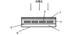
Classifications
-
- H—ELECTRICITY
- H01—ELECTRIC ELEMENTS
- H01L—SEMICONDUCTOR DEVICES NOT COVERED BY CLASS H10
- H01L31/00—Semiconductor devices sensitive to infrared radiation, light, electromagnetic radiation of shorter wavelength or corpuscular radiation and specially adapted either for the conversion of the energy of such radiation into electrical energy or for the control of electrical energy by such radiation; Processes or apparatus specially adapted for the manufacture or treatment thereof or of parts thereof; Details thereof
- H01L31/04—Semiconductor devices sensitive to infrared radiation, light, electromagnetic radiation of shorter wavelength or corpuscular radiation and specially adapted either for the conversion of the energy of such radiation into electrical energy or for the control of electrical energy by such radiation; Processes or apparatus specially adapted for the manufacture or treatment thereof or of parts thereof; Details thereof adapted as photovoltaic [PV] conversion devices
- H01L31/042—PV modules or arrays of single PV cells
- H01L31/048—Encapsulation of modules
- H01L31/049—Protective back sheets
-
- Y—GENERAL TAGGING OF NEW TECHNOLOGICAL DEVELOPMENTS; GENERAL TAGGING OF CROSS-SECTIONAL TECHNOLOGIES SPANNING OVER SEVERAL SECTIONS OF THE IPC; TECHNICAL SUBJECTS COVERED BY FORMER USPC CROSS-REFERENCE ART COLLECTIONS [XRACs] AND DIGESTS
- Y02—TECHNOLOGIES OR APPLICATIONS FOR MITIGATION OR ADAPTATION AGAINST CLIMATE CHANGE
- Y02E—REDUCTION OF GREENHOUSE GAS [GHG] EMISSIONS, RELATED TO ENERGY GENERATION, TRANSMISSION OR DISTRIBUTION
- Y02E10/00—Energy generation through renewable energy sources
- Y02E10/50—Photovoltaic [PV] energy
-
- Y—GENERAL TAGGING OF NEW TECHNOLOGICAL DEVELOPMENTS; GENERAL TAGGING OF CROSS-SECTIONAL TECHNOLOGIES SPANNING OVER SEVERAL SECTIONS OF THE IPC; TECHNICAL SUBJECTS COVERED BY FORMER USPC CROSS-REFERENCE ART COLLECTIONS [XRACs] AND DIGESTS
- Y10—TECHNICAL SUBJECTS COVERED BY FORMER USPC
- Y10T—TECHNICAL SUBJECTS COVERED BY FORMER US CLASSIFICATION
- Y10T428/00—Stock material or miscellaneous articles
- Y10T428/24—Structurally defined web or sheet [e.g., overall dimension, etc.]
- Y10T428/24942—Structurally defined web or sheet [e.g., overall dimension, etc.] including components having same physical characteristic in differing degree
-
- Y—GENERAL TAGGING OF NEW TECHNOLOGICAL DEVELOPMENTS; GENERAL TAGGING OF CROSS-SECTIONAL TECHNOLOGIES SPANNING OVER SEVERAL SECTIONS OF THE IPC; TECHNICAL SUBJECTS COVERED BY FORMER USPC CROSS-REFERENCE ART COLLECTIONS [XRACs] AND DIGESTS
- Y10—TECHNICAL SUBJECTS COVERED BY FORMER USPC
- Y10T—TECHNICAL SUBJECTS COVERED BY FORMER US CLASSIFICATION
- Y10T428/00—Stock material or miscellaneous articles
- Y10T428/249921—Web or sheet containing structurally defined element or component
- Y10T428/249953—Composite having voids in a component [e.g., porous, cellular, etc.]
- Y10T428/249987—With nonvoid component of specified composition
- Y10T428/249991—Synthetic resin or natural rubbers
-
- Y—GENERAL TAGGING OF NEW TECHNOLOGICAL DEVELOPMENTS; GENERAL TAGGING OF CROSS-SECTIONAL TECHNOLOGIES SPANNING OVER SEVERAL SECTIONS OF THE IPC; TECHNICAL SUBJECTS COVERED BY FORMER USPC CROSS-REFERENCE ART COLLECTIONS [XRACs] AND DIGESTS
- Y10—TECHNICAL SUBJECTS COVERED BY FORMER USPC
- Y10T—TECHNICAL SUBJECTS COVERED BY FORMER US CLASSIFICATION
- Y10T428/00—Stock material or miscellaneous articles
- Y10T428/31504—Composite [nonstructural laminate]
- Y10T428/31786—Of polyester [e.g., alkyd, etc.]
- Y10T428/31797—Next to addition polymer from unsaturated monomers
Definitions
- the present invention relates to a film for a solar battery backsheet having a high partial discharge voltage even if it is thin, a solar battery backsheet using the same, and a solar battery using the same.
- FIG. 1 A typical configuration of a general solar cell is shown in FIG.
- a power generating element 3 is sealed with a transparent filler 2 such as EVA (ethylene-vinyl acetate copolymer), and a transparent substrate 4 such as glass and a resin sheet called a back sheet 1 are bonded together. Composed. Sunlight is introduced into the solar cell through the transparent substrate 4. Sunlight introduced into the solar cell is absorbed by the power generation element 3, and the absorbed light energy is converted into electrical energy. The converted electric energy is taken out by a lead wire (not shown in FIG.
- the back sheet 1 is a sheet member that is installed on the back side of the power generation element 3 with respect to the sun and is not in direct contact with the power generation element 3.
- the backsheet 1 polyethylene-based, polyester-based, and fluorine-based resin films are mainly used.
- a bubble-containing film used as a reflective film for a liquid crystal display for a solar battery back sheet Patent Documents 4 and 5.
- solar cells are installed on the roofs of ordinary households and public facilities, or installed on a large site as large-scale power generation.
- the backsheet since a high voltage is applied for a long time when the solar cell system is operated, it is desired that the backsheet has both a long-term mechanical strength and a high electrical resistance. If the electrical resistance is inferior, the discharge of minute charges inside the film called partial discharge occurs during the operation of the solar cell system, and if this continues for a long time, the chemical deterioration of the resin constituting the back sheet proceeds. If chemical degradation progresses due to a partial discharge phenomenon, even if the system has a withstand voltage sufficient to withstand lightning strikes under normal circumstances, when a high voltage is momentarily applied to the system due to lightning strikes, etc., it is fatal. This is because there is a possibility of generating a dielectric breakdown.
- the backsheet is required to increase the voltage at which the partial discharge phenomenon occurs (hereinafter referred to as “partial discharge voltage”) in order to suppress the partial discharge phenomenon even a little.
- partial discharge voltage the voltage at which the partial discharge phenomenon occurs
- JP-A-11-261085 Japanese Patent Laid-Open No. 11-186575 JP 2006-270025 A JP 2009-12454 A JP 2009-42421 A
- the present invention is a film for solar cell backsheet having high mechanical strength and maintaining a mechanical strength over a long period of time, and a solar cell backsheet using the same.
- the solar cell used is to be provided. That is, the present invention has a layered structure having at least two layers and a surface having a surface specific resistance R0 of 10 6 ⁇ / ⁇ or more and 10 14 ⁇ / ⁇ or less (hereinafter referred to as A surface) (A layer).
- B layer a base material layer (B layer), wherein the B layer includes a layer made of polyester (B1 layer), and the mass average molecular weight of the polyester of the B1 layer is 37500 or more and 60000 It is the film for solar cell back sheets which is the following, and a solar cell back sheet and a solar cell using the same.
- the present invention it is possible to provide a film for a solar battery back sheet having a long-term mechanical strength and a high partial discharge voltage even if it is thin. Moreover, by using it, durability improvement of a solar cell backsheet, thickness reduction, etc. are attained, and durability improvement of a solar cell, thickness reduction, etc. are attained.
- the present invention as a result of intensive studies on the above-mentioned problem, that is, retention of mechanical strength over a long period of time and a thin film for a solar battery back sheet having a high partial discharge voltage, controls the electrical characteristics of the surface within a certain range.
- the film for solar cell backsheet of the present invention has the following configuration. That is, a layer (A layer) and a substrate having a laminated structure of at least two layers and having a surface specific resistance R0 of 10 6 ⁇ / ⁇ or more and 10 14 ⁇ / ⁇ or less (hereinafter referred to as A surface).
- the layer (B1 layer) which consists of polyester is included, and when the mass average molecular weight of polyester of this B1 layer shall be 37500 or more and 60000 or less, compared with the conventional backsheet. , The retention of mechanical strength over a long period can be increased.
- the film for solar battery backsheet of the present invention preferably has a surface specific resistance R2 of 10 14 ⁇ / ⁇ or more on the surface opposite to the A surface.
- R2 surface specific resistance
- the surface (6 in FIG. 1) on the opposite side of the resin layer encapsulating the power generating element may be the A surface.
- the partial discharge voltage can be improved.
- a highly durable solar cell can be obtained or the thickness of the solar cell can be reduced.
- the surface specific resistance of both surfaces of the solar cell backsheet film is 10 6 ⁇ / ⁇ or more, the electrical resistance characteristics of the solar cell backsheet may be deteriorated, or electrical energy is taken out from the lead wire. This is because, in some cases, the take-out efficiency is lowered and the power generation efficiency is lowered.
- the film for solar battery backsheet of the present invention preferably has a breaking elongation of 50% or more.
- the elongation at break here is measured based on ASTM-D882 (1999) by cutting a sample into a size of 1 cm ⁇ 20 cm and pulling it at a distance of 5 cm between chucks and a pulling speed of 300 mm / min. More preferably, the elongation determined by the above method is 60% or more, more preferably 80% or more, particularly preferably 100% or more, and most preferably 120% or more.
- the elongation at break is less than 50%, when an impact is applied to the solar cell from the outside when the backsheet using this is incorporated into the solar cell and used.
- the backsheet when a load is applied during vibration during transportation or during work during transportation or construction), the backsheet may break.
- the elongation retention rate to 50% or more, the characteristics of the solar cell against impact can be enhanced.
- the film for solar cell backsheets of this invention is 50% or more of the elongation retention after leaving for 24 hours on the conditions of temperature 125 degreeC and humidity 100% RH.
- the elongation retention here is measured based on ASTM-D882 (1999), and is 24 hours under the conditions of the breaking elongation E0, temperature 125 ° C., and humidity 100% RH of the film before processing. It is a value obtained by the following formula (1) when the elongation at break after standing is E1.
- Elongation retention (%) E1 / E0 ⁇ 100 (1) Note that E1 is a value measured using a sample that was cut into the shape of a measurement piece and then subjected to treatment for 24 hours under conditions of a temperature of 125 ° C. and a humidity of 100%.
- the elongation retention obtained by the above method is 55% or more, more preferably 60% or more, particularly preferably 65% or more, and most preferably 70% or more.
- the elongation retention is less than 50%, the mechanical strength is lowered when used for a long time, and as a result, the use of the solar cell having the backsheet using the same.
- the backsheet may be broken when some external impact is applied to the solar cell (for example, when a falling rock hits the solar cell).
- by setting the elongation retention rate to 50% or more, durability of the mechanical strength of the backsheet during long-term use can be enhanced.
- the solar cell backsheet film of the present invention can be preferably used as long as it satisfies the above-mentioned requirements.
- at least two layers including a conductive layer (A layer) and a base material layer (B layer) are used. It is necessary to have the above laminated structure and at least one side surface should consist of A layer.
- a layer conductive layer
- B layer base material layer
- the layer (A layer) having conductivity of the solar cell backsheet film of the present invention is a surface that becomes 10 6 ⁇ / ⁇ or more and 10 14 ⁇ / ⁇ or less when the surface specific resistance R0 is measured ( A surface). More preferably, it is 10 7 ⁇ / ⁇ or more and 10 14 ⁇ / ⁇ or less, more preferably 10 8 ⁇ / ⁇ or more and 10 14 ⁇ / ⁇ or less, particularly preferably 10 9 ⁇ / ⁇ or more and 10 14 ⁇ / ⁇ or less, most preferably Preferably, it is 10 9 ⁇ / ⁇ or more and 10 13 ⁇ / ⁇ or less.
- the surface specific resistance R0 of the A layer is less than 10 6 ⁇ / ⁇ , the A layer becomes too easy to conduct electricity and also conducts in the thickness direction. As a result, the entire A layer acts as a pseudo electrode, The effect of relaxing the electric field in the direction is lost, and the partial discharge voltage may not be improved. When electric energy is extracted from the lead wire, the extraction efficiency may decrease and the power generation efficiency may decrease. Further, if the surface specific resistance R0 of the A layer exceeds 10 14 ⁇ / ⁇ , the conductivity is too small and the effect of relaxing the electric field in the plane direction is lost, and the partial discharge voltage may not be improved. Absent.
- the electric field applied in the film thickness direction when a high voltage is applied by controlling the surface specific resistance R0 of the A layer of the film for solar battery backsheet of the present invention to a range of 10 6 ⁇ / ⁇ or more and 10 14 ⁇ / ⁇ or less. It is possible to moderately conduct a part of the film in the direction of the film surface, and to reduce the concentration of the electric field in the thickness direction, and it is possible to increase the partial discharge voltage without increasing the film thickness. Moreover, the partial discharge characteristics and electrical resistance characteristics of the backsheet using this film can be dramatically improved.
- the layer A in the film for solar battery backsheet of the present invention has a surface specific resistance R1 of A surface after being allowed to stand for 24 hours at a temperature of 125 ° C. and a humidity of 100% of 10 6 ⁇ / ⁇ or more and 10 14 ⁇ / ⁇ or less.
- a surface specific resistance R1 of A surface after being allowed to stand for 24 hours at a temperature of 125 ° C. and a humidity of 100% of 10 6 ⁇ / ⁇ or more and 10 14 ⁇ / ⁇ or less.
- R1 surface specific resistance
- R1 of A surface after being allowed to stand for 24 hours at a temperature of 125 ° C.
- a humidity of 100% of 10 6 ⁇ / ⁇ or more and 10 14 ⁇ / ⁇ or less Preferably there is. More preferably, it is 10 7 ⁇ / ⁇ or more and 10 14 ⁇ / ⁇ or less, more preferably 10 8 ⁇ / ⁇ or more and 10 14 ⁇ / ⁇ or less
- the surface specific resistance R1 of the A surface after processing is less than 10 6 ⁇ / ⁇ , the effect of relaxing the electric field in the surface direction is lost during long-term use, and the partial discharge voltage is reduced. Sometimes, the power generation efficiency of the solar cell may decrease. On the other hand, if it exceeds 10 14 ⁇ / ⁇ , the conductivity becomes too low and the effect of relaxing the electric field in the surface direction is lost, and the partial discharge voltage may be lowered.
- partial discharge voltage is maintained even in long-term use by controlling the surface specific resistance R1 of the processed layer A to a range of 10 6 ⁇ / ⁇ to 10 14 ⁇ / ⁇ . It is possible to maintain the improvement effect. As a result, it becomes possible to enhance the durability of the partial discharge characteristics and electric resistance characteristics of the backsheet using the film for solar battery backsheet of the present invention.
- the A surface only needs to satisfy the above-mentioned characteristics, and specific examples thereof include the inclusion of a component that develops conductivity in the A layer.
- a component that develops conductivity any of organic conductive materials, inorganic conductive materials, and organic / inorganic composite conductive materials can be preferably used.
- organic conductive materials include cationic conductive compounds having cationic substituents such as ammonium groups, amine bases, and quaternary ammonium groups in the molecule, sulfonate groups, phosphate groups, and carboxylate groups.
- Anionic conductive compounds having anionic properties such as, ionic conductive materials such as anionic substituents, amphoteric conductive compounds having both cationic substituents, polyacetylene having a conjugated polyene skeleton, poly Examples thereof include conductive polymer compounds such as paraphenylene, polyaniline, polythiophene, polyparaphenylene vinylene, and polypyrrole.
- These conductive materials are introduced into the matrix material constituting the A layer by the following methods 1) to 4), and any of them is preferably used. Thereby, it becomes possible to express the A layer conductivity. That is, 1) Copolymerizing a conductive skeleton to the matrix material; 2) Add, mix, and dissolve conductive materials into the matrix material. 3) After adding and mixing the conductive material to the matrix material, the conductive material is transferred to the surface and concentrated near the surface. 4) Add and mix conductive materials into the matrix material and disperse to form a conductive network. It is possible to express conductivity in the A layer by a method such as these, and any of them is preferably used.
- conductive materials particularly when forming a film as a solution film, or when forming a layer A by coating on a base material layer (layer B), when applying a high voltage
- an ionic conductive material is preferable, and a cationic conductive compound is more preferable in that it has an effect of improving applicability, adhesion, and partial discharge voltage over a long period of time.
- these conductive compounds it is preferable to use any of low molecular weight type conductive compounds, high molecular weight type conductive compounds, and the like.
- high molecular weight type conductive compounds are preferably used from the viewpoint of durability and the like.
- organic conductive materials can be preferably used either water-soluble or water-insoluble, but the surface A of the solar battery backsheet film of the present invention preferably has moisture and heat resistance. It is preferable to use a water-soluble conductive compound.
- water solubility and water insolubility are determined by the monomer species constituting these materials, and in order to achieve water insolubility, the monomer species having the functional group and the functional group The ratio of the number of moles of monomer species having the functional group to the number of moles of monomer species having no functional group (the number of moles of monomer species having the functional group).
- Number of moles of monomer species having no functional group is preferably from 10/90 to 90/10, more preferably from 20/80 to 80/20, still more preferably from 30/70 to 70/30. is there.
- the ratio is smaller than 10/90, the surface specific resistance R0 of the A surface of the formed A layer becomes too high, and the partial discharge voltage improving effect may be lost.
- water solubility will become high when ratio exceeds 90/10, the heat-and-moisture resistant property of the formed A surface may be inferior.
- the copolymerization ratio between the monomer species having the functional group and the monomer species not having the functional group is controlled to be 10/90 or more and 90/10 or less. It is possible to improve the discharge voltage and to impart the heat and humidity resistance of the characteristics.
- the conductive material used for the A layer is an organic conductive material, for improving the heat and moisture resistance, improving the strength of the A layer, etc.
- the organic conductive material in addition to the organic conductive material, when applying by the in-line coating method at the time of manufacturing the material layer (B layer), as a material constituting a matrix constituting the A layer Water-insoluble such as polyester resin, acrylic resin, polyolefin resin, polyamide resin, polycarbonate, polystyrene, polyether, polyester amide, polyether ester, polyvinyl chloride, polyvinyl alcohol and copolymers containing these as components It is also preferable to use a functional resin.
- the mixing ratio of the organic conductive material and the water-insoluble resin is 5/95 or more when the organic conductive material is a water-soluble conductive material. 50/50 or less is preferable.
- the mixing ratio is less than 5/95, the surface specific resistance R0 of the A layer is increased, and the partial discharge voltage may not be improved, which is not preferable.
- the mixing ratio is greater than 5/95 than 50/50, The formed layer A may be inferior in heat and moisture resistance.
- the organic conductive material is a water-insoluble conductive material
- the mixing ratio of the organic conductive material and the water-insoluble resin is 26/74 or more and 98/2 or less are preferable. More preferably, it is 30/70 or more and 95/5 or less.
- the mixing ratio is less than 26/74, the surface specific resistance R0 of the A layer is increased, and the partial discharge voltage may not be improved, which is not preferable. If the mixing ratio is more than 98/2, the formed A The moisture and heat resistance of the layer may be inferior.
- Partial discharge voltage is improved by controlling the mixing ratio of the organic conductive material and the water-insoluble resin (the mass of the organic conductive material / the mass of the water-insoluble resin) to 26/74 or more and 98/2 or less. Further, it becomes possible to impart moisture and heat resistance to the characteristics.
- Examples of the water-insoluble resin when the A layer is formed by melt extrusion include polyethylene terephthalate (hereinafter sometimes abbreviated as “PET”), polyethylene-2,6-naphthalate, polypropylene terephthalate, and polybutylene.
- PET polyethylene terephthalate
- polyethylene-2,6-naphthalate polyethylene-2,6-naphthalate
- polypropylene terephthalate polypropylene terephthalate
- polybutylene polybutylene
- Polyester resins such as terephthalate, poly 1,4-cyclohexylene dimethylene terephthalate, polylactic acid, polyolefin resins such as polyethylene, polystyrene, polypropylene, polyisobutylene, polybutene, polymethylpentene, cycloolefin resins, polyamide resins, Polyimide resin, polyether resin, polyesteramide resin, polyetherester resin, acrylic resin, polyurethane resin, polycarbonate resin, polyvinyl chloride resin, fluorine resin, etc. It is possible to use.
- polyolefin resins such as polyethylene, polystyrene, polypropylene, polyisobutylene, polybutene, polymethylpentene, cycloolefin resins, polyamide resins, Polyimide resin, polyether resin, polyesteramide resin, polyetherester resin, acrylic resin, polyurethane resin, polycarbonate resin, polyvinyl chloride resin, fluorine resin, etc. It is possible
- polyester resins because of the variety of monomer types to be copolymerized and the ease of adjustment of material properties, it is possible to use polyester resins, polyolefin resins, cycloolefin resins, polyamide resins, acrylic resins, It is preferably mainly composed of a thermoplastic resin selected from a fluororesin or a mixture thereof. Particularly preferably, it is preferably composed mainly of a polyester-based resin from the viewpoint of mechanical strength and cost, and further, the water-insoluble resin is uniaxially or biaxially oriented, whereby the mechanical strength is improved by orientation crystallization. In the case of a polyester resin or the like, the hydrolysis resistance of the A layer during long-term use can be improved.
- the substrate layer in the case where the moisture and heat resistance characteristics are further improved, or when the A layer is coated on the substrate layer (B layer))
- the substrate layer in the case of improving the adhesion with the (B layer), in particular, when forming a film as a solution casting, or when coating the A layer on the base material layer (B layer), the blocking of the film can be prevented.
- a resin or a compound that undergoes a crosslinking reaction with a functional group present in the above-described organic material and / or a resin constituting the water-insoluble resin, such as a hydroxyl group, a carboxyl group, a glycidyl group, an amide group, or the like is preferably used.
- a functional group present in the above-described organic material and / or a resin constituting the water-insoluble resin such as a hydroxyl group, a carboxyl group, a glycidyl group, an amide group, or the like
- examples thereof include methylolated or alkylolated urea, melamine, acrylamide, polyamide resins and epoxy compounds, oxetane compounds, isocyanate compounds, coupling agents, aziridine compounds, oxazoline compounds, carbodiimides, etc.
- System compounds, acid anhydrides, carboxylic acid ester derivatives, and mixtures thereof can be used.
- the kind and content of the crosslinking agent are appropriately selected depending on the organic conductive material constituting the A layer, the water-insoluble resin, the base material layer (B layer), and the like.
- a crosslinking agent in the solar battery backsheet film of the present invention when forming a film as a solution film, or when coating a base material layer (B layer) as an A layer, an organic conductive material and / or When the water-insoluble resin has an acrylic skeleton, an oxazoline compound is used as a crosslinking agent.
- a melamine compound is used as a crosslinking agent.
- the formed A layer is more preferable in that it has better moisture and heat resistance.
- a crosslinking agent in the case of using a polyester resin as the water-insoluble resin, an oxazoline compound, an epoxy compound, an oxetane compound, a carbodiimide compound, an acid anhydride, Carboxylic acid ester derivatives are preferably used.
- the addition amount of the crosslinking agent is usually preferably 0.01 parts by mass or more and 50 parts by mass or less, more preferably 0.2 parts by mass or more and 40 parts by mass or less, with respect to 100 parts by mass of the total resin component constituting the A layer. More preferably, the range of 0.5 to 30 parts by mass is more preferable.
- any of a heating system, an electromagnetic wave irradiation system, a moisture absorption system, etc. may be used, but usually a method by heating is preferably used.
- the surface specific resistance R0 of the A surface is the type of the organic conductive material contained in the A layer, water-insoluble It depends on the type and mixing ratio of the resin and the crosslinking agent, the mixing ratio with other materials, the film thickness, and the like.
- the surface specific resistance R0 increases as the proportion of the water-insoluble resin and the crosslinking agent increases with respect to the organic conductive material contained in the A layer, and the surface specific resistance R0 decreases as the ratio decreases.
- the surface specific resistance R0 decreases as the film thickness of the A layer increases, and the surface specific resistance R0 increases as it decreases.
- the optimal composition, film thickness, and the like vary depending on the type of material used, the film configuration, and the like, but are formed so that the surface specific resistance R0 of the A surface satisfies the above-described requirements.
- the material constituting the A layer is an organic conductive material and the A layer is coated by an in-line coating method during the production of the base material layer (B layer)
- a cation having an acrylic skeleton as a conductive material is more preferable because it imparts the film formability of the A layer and has a high partial discharge voltage and high heat and humidity resistance even when the obtained A layer is thin.
- a combination of a system conductive compound, a compound having an acrylic skeleton as a water-insoluble resin, and a combination of an oxazoline compound as a crosslinking agent is preferable.
- the organic conductive material contains 50 parts by mass or more as 100 parts by mass of the total resin component, and the mixing ratio of the organic conductive material and the water-insoluble resin (mass of organic conductive material / water-insoluble Of the resin) is 25/75 or more and 98/2 or less (more preferably 50/50 or more and 95/5 or less), and the ratio of the crosslinking agent is 1 part by mass or more and 20 parts by mass or less (100 parts by mass of the total resin components). More preferably, it is 2 parts by mass or more and 20 parts by mass or less.
- the material constituting the conductive layer (A layer) is an inorganic conductive material
- examples include gold, silver, copper, platinum, silicon, boron, Palladium, rhenium, vanadium, osmium, cobalt, iron, zinc, ruthenium, praseodymium, chromium, nickel, aluminum, tin, zinc, titanium, tantalum, zirconium, antimony, indium, yttrium, lanthanum, magnesium, calcium, cerium, hafnium, Oxidized, sub-oxidized, hypo-sub-oxidized materials containing an inorganic group such as barium as the main component, or a mixture of the above-mentioned inorganic group and the above-mentioned inorganic group oxidized, sub-oxidized, sub-oxidized These are referred to as inorganic oxides), and those containing the above inorganic group as the main component Or a mixture of the inorganic substance group
- Inorganic oxynitride carbonized, sub-carbonized, hypo-sub-carbonized with the main component of the inorganic group, or carbonized, sub-carbonized, hypo-carbonized with the inorganic group and inorganic group.
- a mixture with the above hereinafter referred to as “inorganic carbide”), and those containing the above inorganic group as the main component are fluorinated and / or chlorinated and / or brominated and / or iodinated (hereinafter referred to as “halogen”).
- Subhalogenated, hypohalogenated, and a mixture of the inorganic group and the inorganic group halogenated, subhalogenated, or subhalogenated hereinafter referred to as “inorganic halide”.
- inorganic halide a mixture of the above inorganic substance group and the above inorganic substance group sulfided, subsulfided, hyposulfurized (hereinafter referred to as inorganic sulfide), and the above compound doped with a different element
- examples thereof include carbon-based compounds such as graphite-like carbon, diamond-like carbon, carbon fiber, carbon nanotube, and fullerene (hereinafter referred to as carbon-based compounds), and mixtures thereof.
- the above material may be contained at least in the A layer, but when the layer thickness of the A layer is 1 ⁇ m or less, in order to make the surface resistivity within the above range, it is more preferable to use the main component. Good. In addition, the case where it exceeds 50 mass% in this layer is defined as a main component.
- the surface specific resistance R0 of the A surface of the A layer is the inorganic group contained in the film. It is determined by the degree of modification (oxidation, nitridation, oxynitridation, carbonization, halogenation, sulfidation, etc.), the mixing ratio between the inorganic group and the modified inorganic group, the mixing ratio with other materials, the film thickness, and the like. The higher the degree of modification of the inorganic group, the higher the surface specific resistance R0 of the A surface, and the lower the degree of modification, the smaller the surface specific resistance R0 of the A surface.
- the surface specific resistance R0 increases as the ratio of the modified inorganic group to the inorganic group included in the A layer increases, and the surface specific resistance R0 decreases as the ratio decreases. Moreover, the surface specific resistance R0 becomes low as the film thickness increases, and the surface specific resistance R0 increases as the film thickness decreases.
- the optimum composition and film thickness vary depending on the metal species to be used, the modification method, etc., but the surface specific resistance R0 is formed so as to satisfy the above requirements.
- the material constituting the A layer is an organic / inorganic composite conductive material (for example, i) a non-conductive water-insoluble resin is used as a matrix
- an inorganic conductive material is used as a conductive material
- an organic conductive material and an inorganic conductive material are used in combination
- an inorganic nonconductive material is used in combination with the organic conductive material Iv)
- inorganic conductive material, water-insoluble resin, and crosslinking agent In addition, an inorganic non-conductive material is appropriately combined.
- a structure in which a water-insoluble resin is used as the matrix of the A layer and an inorganic conductive material is dispersed may be mentioned.
- the water-insoluble resin those similar to those used in the case of the organic conductive material are preferably used.
- the shape of the inorganic conductive material dispersed in the water-insoluble resin serving as the matrix of the A layer is not particularly limited, such as a true spherical shape, a spheroid shape, a flat shape, a bead shape, a plate shape, or a needle shape. .
- fine-particles connected two-dimensionally or three-dimensionally in the water-insoluble resin is also contained.
- These inorganic particles may be composed of a single element or a plurality of elements.
- the inorganic conductive material zinc oxide, titanium oxide, cesium oxide, antimony oxide, tin oxide, indium tin oxide, oxide are easily dispersed in the incompatible resin as the matrix of the A layer.
- Metal oxides such as yttrium, lanthanum oxide, zirconium oxide, aluminum oxide, and silicon oxide, and carbon-based fine particles such as carbon black, carbon fiber, carbon nanotube, and fullerene are preferably used.
- the average particle diameter of the inorganic conductive material is arbitrary, but is preferably 0.001 ⁇ m or more and 20 ⁇ m or less.
- the particle diameter here refers to the median diameter d50.
- the particle size is 0.001 ⁇ m or less, it may be difficult to disperse in the water-insoluble resin as a matrix, and when it is 20 ⁇ m or more, a uniform A layer may be formed. It becomes difficult.
- the average particle size of the inorganic conductive material it is possible to achieve both conductivity and uniformity of the formed film.
- the mechanical strength and heat-and-moisture resistance are further improved, and particularly the adhesiveness with the base material layer (B layer) when coated on the base material layer (B layer) as the A layer is improved.
- a crosslinking agent in order to prevent blocking in the case of forming a film as a film or when coating the base layer (B layer) as the A layer. Is called.
- the crosslinking agent the same ones as those used in the case of the organic conductive material are preferably used.
- the improvement of the slipperiness of the A layer and the blocking resistance it is also preferable to include fine particles for application, glossiness adjustment, surface resistivity control and the like.
- fine particles for application, glossiness adjustment, surface resistivity control and the like.
- inorganic fine particles or organic fine particles can be used.
- the inorganic fine particles include gold, silver, copper, platinum, palladium, rhenium, vanadium, osmium, cobalt, iron, zinc, ruthenium, praseodymium, chromium, nickel, aluminum, tin, zinc, titanium, tantalum, zirconium, Fine particles of metals such as antimony, indium, yttrium, and lanthanium, fine particles of carbon compounds such as graphite-like carbon and diamond-like carbon, fine particles made of inorganic conductive materials such as carbon nanotubes and fullerenes, zinc oxide, titanium oxide, cesium oxide , Antimony oxide, tin oxide, indium tin oxide, yttrium oxide, lanthanum oxide, zirconium oxide, aluminum oxide, metal oxide such as silicon oxide, lithium fluoride, magnesium fluoride, aluminum fluoride Metal inorganic fluorides such as um and cryolite, metal phosphates such as calcium phosphate, carbonates such as calcium carbonate,
- the particle diameter (number average particle diameter) of these fine particles is preferably 0.05 ⁇ m or more and 15 ⁇ m or less, and preferably 0.1 ⁇ m or more and 10 ⁇ m or less. Moreover, as content, 5 mass% or more and 50 mass% or less are preferable with respect to all the resin components which comprise A layer, More preferably, it is 6 mass% or more and 30 mass% or less, More preferably, it is 7 mass% or more and 20 mass%. It is as follows. By controlling the surface specific resistance within the above range by adjusting the particle size of the contained particles to the above range, it is possible to impart surface slipperiness or adjust the surface glossiness. preferable.
- a laminated structure of at least two layers including a conductive layer (A layer) and a base material layer (B layer) is used, and non-conductive in the inorganic conductive material constituting the A layer.
- distributed water-soluble water-soluble resin is mentioned.
- the inorganic conductive material the same materials as those used in the case of the inorganic conductive material are preferably used.
- the shape of the water-insoluble resin dispersed in the inorganic conductive material is not particularly limited, such as a true spherical shape, a spheroid shape, a flat shape, a bead shape, a plate shape, or a needle shape.
- water-insoluble resins may be made of a single resin or may be made of a plurality of resins.
- the same water-insoluble resin as that used in the case of the organic conductive material is preferably used, and a silicone compound, a crosslinked styrene, a crosslinked acryl, a crosslinked melamine is used.
- Cross-linked fine particles such as can also be used.
- the A layer preferably contains a light stabilizer in order to prevent ultraviolet degradation of the A layer and / or the base material layer (B layer).
- the light stabilizer is a compound that absorbs light such as ultraviolet rays and converts it into heat energy, a material that captures radicals generated by the absorption and decomposition of the A layer and suppresses the decomposition chain reaction, etc. Is mentioned. More preferably, a compound that absorbs light such as ultraviolet rays and converts it into thermal energy is used.
- the effect of improving the partial discharge voltage by the A surface of the A layer can be kept high over a long period of time. Changes in color tone, strength deterioration, and the like due to ultraviolet rays of the layer and / or the base material layer (B layer) are prevented.
- the ultraviolet absorber here is within a range in which other properties are not impaired, an organic ultraviolet absorber, an inorganic ultraviolet absorber, and a combination thereof can be preferably used without any particular limitation. It is desirable that it has excellent heat and humidity resistance and can be uniformly dispersed in the A layer.
- ultraviolet absorbers examples include, for example, in the case of organic ultraviolet absorbers, salicylic acid-based, benzophenone-based, benzotriazole-based, cyanoacrylate-based ultraviolet absorbers, hindered amine-based ultraviolet stabilizers, etc. Is mentioned.
- salicylic acid-based pt-butylphenyl salicylate p-octylphenyl salicylate
- benzophenone-based 2,4-dihydroxybenzophenone 2-hydroxy-4-methoxybenzophenone, 2-hydroxy-4-methoxy -5-sulfobenzophenone, 2,2 ', 4,4'-tetrahydroxybenzophenone, bis (2-methoxy-4-hydroxy-5-benzoylphenyl) methane
- UV absorbers triazine-based ultraviolet absorbers are more preferable in that they have high resistance to repeated ultraviolet absorption.
- these ultraviolet absorbers may be added to the A layer by the above-mentioned ultraviolet absorber alone, or a form in which an organic conductive material or a water-insoluble resin is copolymerized with a monomer having an ultraviolet absorber function. May be introduced.
- examples of inorganic ultraviolet absorbers include metal oxides such as titanium oxide, zinc oxide, and cerium oxide, and carbon-based materials such as carbon, fullerene, carbon fiber, and carbon nanotube.
- these ultraviolet absorbers may be added to the layer A as a single component of the above-mentioned ultraviolet absorber, or may be combined with an inorganic conductive material or introduced into an organic conductive material or a water-insoluble resin. May be.
- the ultraviolet absorber may be used alone or in combination of two or more kinds, and an inorganic or organic compound may be used in combination.
- the content of the ultraviolet absorber in the layer A of the solar battery backsheet film of the present invention is 0.05% by mass or more and 20% by mass or less with respect to the total solid components in the layer A. Preferably, it is 0.1 to 15% by mass, more preferably 0.15 to 15% by mass.
- the content of the UV absorber is less than 0.05% by mass, the light resistance is insufficient, and the A layer is deteriorated during long-term use, and the partial discharge voltage may be lowered. If it is more than 20% by mass, the coloring of the A layer may be increased.
- the total solid component of the A layer is 1% by mass to 50% by mass, more preferably 2% by mass to 45% by mass, and further preferably 5% by mass to 40% by mass. Especially preferably, it is 8 mass% or more and 35 mass% or less, Most preferably, it is 12 mass% or more and 30 mass% or less.
- the content of the ultraviolet absorber in the A layer may be reduced to an organic ultraviolet ray.
- the absorbent 0.05% by mass or more and 20% by mass or less with respect to the total solid components in the A layer.
- the total solid component of the A layer is 1% by mass or more and 50% by mass or less.
- the thickness of the A layer is preferably 0.001 ⁇ m or more and 50 ⁇ m or less.
- the material constituting the A layer is mainly composed of an organic material and the A layer is formed by coating, it is usually preferably 0.01 ⁇ m or more and 50 ⁇ m or less, and the base material layer (B layer) is particularly uniaxial or
- the A layer is formed during the production of the biaxially stretched film, it is preferably 0.01 ⁇ m or more and 1 ⁇ m or less, more preferably 0.02 ⁇ m or more from the viewpoint of the ease of forming the A layer and uniformity. 1 ⁇ m or less, more preferably 0.05 ⁇ m or more and 1 ⁇ m or less.
- the material constituting the A layer is mainly composed of an inorganic material, it is preferably 0.001 ⁇ m or more and 1 ⁇ m or less.
- the layer is formed by a dry method such as a vapor deposition method or a sputtering method, A
- the thickness is more preferably 0.005 ⁇ m to 0.8 ⁇ m, and still more preferably 0.01 ⁇ m to 0.5 ⁇ m.
- the preferable thickness of the A layer is 0.05 ⁇ m or more and 50 ⁇ m or less. More preferably, they are 1 micrometer or more and 50 micrometers or less, More preferably, they are 2 micrometers or more and 30 micrometers or less, Most preferably, they are 3 micrometers or more and 20 micrometers or less, Most preferably, they are 3 micrometers or more and 15 or less.
- the base material layer (B layer) in the film for solar cell backsheet of the present invention is an organic film base material such as polyester resin, polyolefin resin, acrylic resin, polyamide resin, polyimide resin, polyether resin, polycarbonate resin, Metal base materials such as silicon, glass, stainless steel, aluminum, aluminum alloy, iron, steel, and titanium, inorganic base materials such as concrete, organic-inorganic composite base materials such as silicon-based resins, and combinations thereof are applicable.
- a flexible base material containing an organic material from the viewpoint of handling and weight reduction. More preferably, the main component is made of a thermoplastic resin.
- thermoplastic resin examples include polyethylene terephthalate, polyethylene-2,6-naphthalate, polypropylene terephthalate, polybutylene terephthalate, poly-1,4-cyclohexylene dimethylene terephthalate, polyester resin such as polylactic acid, polyethylene, polystyrene, Polyolefin resins such as polypropylene, polyisobutylene, polybutene, and polymethylpentene, cycloolefin resins, polyamide resins, polyimide resins, polyether resins, polyesteramide resins, polyetherester resins, acrylic resins, polyurethane Resin, polycarbonate resin, polyvinyl chloride resin, fluorine resin and the like can be used.
- polyester resin such as polylactic acid, polyethylene, polystyrene
- Polyolefin resins such as polypropylene, polyisobutylene, polybutene, and polymethylpentene
- cycloolefin resins polyamide resin
- polyester resins because of the variety of monomer types to be copolymerized and the ease of adjustment of material properties, it is possible to use polyester resins, polyolefin resins, cycloolefin resins, polyamide resins, acrylic resins, It is preferably mainly composed of a thermoplastic resin selected from a fluororesin or a mixture thereof. Particularly preferably, the polyester resin is mainly constituted from the viewpoint of mechanical strength and cost.
- the main repeating units are ethylene terephthalate, ethylene Those comprising -2,6-naphthalenedicarboxylate, propylene terephthalate, butylene terephthalate, 1,4-cyclohexylenedimethylene terephthalate, ethylene-2,6-naphthalenedicarboxylate, and mixtures thereof are preferably used.
- the main repeating unit means that the total of the above repeating units is 70 mol% or more, more preferably 80 mol% or more, more preferably 90 mol% or more of all repeating units of the polyester resin. Particularly preferred from the viewpoint of mechanical strength and heat resistance.
- ethylene terephthalate, ethylene-2,6-naphthalenedicarboxylate, and mixtures thereof are preferably the main constituents in that they can be easily polymerized at low cost and have excellent heat resistance.
- ethylene terephthalate when more ethylene terephthalate is used as a structural unit, a cheaper and more versatile film having moisture and heat resistance can be obtained, and more ethylene-2,6-naphthalenedicarboxylate is used as a structural unit. When used, the film can be made more excellent in heat and moisture resistance.
- the B layer includes a layer made of polyester (B1 layer). Moreover, it is preferable to use the above-described polyester as the polyester constituting the B1 layer.
- the mass average molecular weight Mw1 of the polyester constituting the B1 layer needs to be 37500 or more and 60000 or less.
- the mass average molecular weight referred to here is a value obtained by gel permeation chromatography, a molecular weight calibration curve is prepared using PET-DMT (standard product), and a value obtained based on the molecular weight calibration curve. That is.
- a gel permeation chromatograph equipped with two Shodex HFIP 806M (manufactured by Showa Denko KK) as a column and an RI type differential refractometer (2414 type, sensitivity 256, manufactured by WATERS) as a detector.
- GCP-244 manufactured by WATERS
- GPC measurement is performed using PET-DMT (standard product) at room temperature (23 ° C.) at a flow rate of 0.5 mL / min.
- V elution volume
- M molecular weight
- Mass average molecular weight (Mw) ⁇ (Ni ⁇ Mi 2 ) / ⁇ (Ni ⁇ Mi) (3) (Here, Ni is the molar fraction, and Mi is the molecular weight of each elution position of the GPC curve obtained via the molecular weight calibration curve.) If the B1 layer used for such measurement contains organic fine particles, inorganic fine particles, metals, metal salts, other additives and other components that are insoluble in the solvent, filtration with a filter, centrifugation, etc. This is a value obtained by preparing a solution again after removing insoluble components.
- the B1 layer may contain additives such as plasticizers, surfactants, dyes, etc., after removing insoluble components, reprecipitation method, recrystallization method, chromatography method, extraction method After removing the insoluble additive in the same manner as described above, the solution is prepared again and measured.
- additives such as plasticizers, surfactants, dyes, etc.
- the mass average molecular weight of the B1 layer is preferably 37500 or more and 60000 or less, more preferably 38500 or more and 58000 or less, and further preferably 40000 or more and 55000 or less.
- the mass average molecular weight of the polyester resin constituting the B1 layer is less than 37500, it is inferior in heat-and-moisture resistance properties, hydrolysis proceeds during long-term use, and as a result, the mechanical strength may decrease, which is not preferable.
- it exceeds 60,000 it is not preferable because polymerization becomes difficult, or even if polymerization is possible, it becomes difficult to extrude the resin with an extruder and film formation becomes difficult.
- the mass average molecular weight of the B1 layer constituting the B layer is in the range of 37500 or more and 60000 or less, both film forming property and hydrolysis resistance can be achieved.
- the base material layer (B layer) has a laminated structure
- the number average molecular weights of the polyester which comprises B1 layer are 8000-40000.
- the number average molecular weight of the polyester of the B1 layer is more preferably 9500 or more and 40000 or less, further 10,000 or more and 40000 or less, further 10500 or more and 40000 or less, and further 11000 or more and 40000 or less. Further, it is 18500 or more and 40000 or less, further 19000 or more and 35000 or less, and particularly preferably 20000 or more and 33000 or less.
- the number average molecular weight of the polyester resin constituting the B1 layer is less than 8000, the heat and moisture resistance is inferior and hydrolysis proceeds during long-term use, resulting in a decrease in mechanical strength. Moreover, when it exceeds 40,000, even if superposition
- the intrinsic viscosity (IV) of the polyester of the B1 layer is preferably 0.65 or more. More preferably, it is 0.68 or more, More preferably, it is 0.7 or more, Most preferably, it is 0.72 or more. If IV is less than 0.65, the retention of mechanical strength during long-term use may be reduced. In the polyester film of the present invention, when the IV of the polyester resin constituting the polyester layer (P layer) is 0.65 or more, the retention of mechanical strength during long-term use can be suppressed.
- the upper limit of IV is not particularly determined, it is preferably 1.0 or less, more preferably 0.9 from the viewpoint that the polymerization time is long, which is disadvantageous in cost and difficult to melt extrusion. It is as follows. *
- the B1 layer constituting the B layer is preferably uniaxially or biaxially oriented.
- a plane orientation coefficient indicating the degree of orientation is preferably 0.16 or more. More preferably, it is 0.162 or more, Furthermore, it is 0.165 or more. If the plane orientation coefficient is less than 0.16, the heat and moisture resistance may not be improved.
- high moisture and heat resistance can be obtained by setting the plane orientation coefficient to 0.16 or more.
- the minute endothermic peak temperature TmetaB1 of the B1 layer and the melting point TmB1 of the B1 layer obtained by differential scanning calorimetry (DSC) satisfy the following formula (5).
- TmetaB1 and melting point TmB1 of the B1 layer mentioned here are values in a temperature raising process (temperature raising rate: 20 ° C./min) obtained by differential scanning calorimetry (hereinafter, DSC). Specifically, by a method based on JIS K-7121 (1999), heating from 25 ° C. to 300 ° C. at a heating rate of 20 ° C./min (1stRUN), holding in that state for 5 minutes, and then 25 ° C.
- TmetaB1 is defined as the peak top temperature in the crystal melting peak of 2ndRun.
- TmB1-TmetaB1 More preferably, 50 ° C. ⁇ TmB1-TmetaB1 ⁇ 80 ° C., and still more preferably 55 ° C. ⁇ TmB1-TmetaB1 ⁇ 75 ° C. If TmB1-TmetaB1 exceeds 90 ° C, the residual stress at the time of stretching is insufficient, and as a result, the thermal shrinkage of the film becomes large, and it becomes difficult to bond in the bonding process when assembled in a solar cell. Even if they are pasted together, the solar cell system may be greatly warped when incorporated into a solar cell and used at high temperatures.
- TmB1-TmetaB1 is less than 40 ° C., the orientation crystallinity is lowered and the hydrolysis resistance may be inferior.
- TmetaB1 of the B1 layer constituting the B layer is preferably 160 ° C. or higher and TmB1-40 ° C. (where TmB1-40 ° C.> 160 ° C.). More preferably, it is 170 ° C.
- TmB1-50 ° C. (where TmB1-50 ° C.> 170 ° C.), and more preferably TmetaB1 is 180 ° C. or higher and TmB1-55 ° C. (where TmB1-55 ° C.> 180 ° C.).
- TmetaB1 is less than 160 ° C., the heat resistance of the film is low, and the durability as a back sheet may be lowered.
- the melting point TmB1 of the B1 layer constituting the B layer is preferably 220 ° C. or higher in view of heat resistance, more preferably 240 ° C. or higher, more preferably 250 ° C. It is.
- the upper limit of the melting point TmB1 of the B1 layer is not particularly limited, but is preferably 300 ° C. or less in view of productivity.
- the number of carboxylic acid terminal groups of the B1 layer constituting the B layer is preferably 20 equivalents / t or less, more preferably 15 equivalents / t or less, and still more preferably 13 equivalents / t. t or less, particularly preferably 10 equivalent / t or less. If it exceeds 15 equivalents / t, hydrolysis due to catalysis by protons of carboxylic acid end groups is promoted and deterioration tends to proceed.
- the dicarboxylic acid component and the diol component are esterified and discharged when the melt viscosity reaches a predetermined melt viscosity.
- Method 3) It can be obtained by a combination of a method of adding a buffering agent or a terminal blocking agent at the time of molding, and the like.
- the polyester constituting the B1 layer preferably contains a buffering agent in an amount of 0.1 mol / t to 5.0 mol / t.
- the buffer of the present invention is a substance that is soluble in the diol residue component of the polyester constituting the B1 layer, such as ethylene glycol, and dissociates after dissolution and exhibits ionicity.
- the polyester constituting the B1 layer contains a buffering agent, whereby the initial number of carboxyl group terminals can be further reduced and hydrolysis reaction can be suppressed.
- the neutralization of protons acting as a catalyst for the hydrolysis reaction at the end of the carboxyl group newly generated by the hydrolysis reaction can further suppress the hydrolysis reaction, thereby further suppressing the wet heat degradation of the polyester film. It becomes possible.
- the buffering agent is preferably an alkali metal salt from the viewpoint of polymerization reactivity and heat and humidity resistance, for example, phthalic acid, citric acid, carbonic acid, lactic acid, tartaric acid, phosphoric acid, phosphorous acid, Mention may be made of alkali metal salts with compounds such as hypophosphorous acid and polyacrylic acid. Among them, potassium and sodium are preferable as alkali metal elements from the viewpoint of hardly generating precipitates due to catalyst residues.
- sodium dihydrogen, sodium hydrogen phosphite, potassium hydrogen phosphite, sodium hypophosphite, potassium hypophosphite, and sodium polyacrylate examples thereof include sodium dihydrogen, sodium hydrogen phosphite, potassium hydrogen phosphite, sodium hypophosphite, potassium hypophosphite, and sodium polyacrylate.
- an alkali metal salt represented by the following formula is preferable from the viewpoint of polymerization reactivity of the polyester constituting the B1 layer and heat resistance during melt molding, and the alkali metal is sodium and / or potassium.
- the alkali metal is sodium and / or potassium.
- phosphoric acid and sodium and / or potassium metal salts are particularly preferable in view of polymerization reactivity and heat and humidity resistance.
- content of a buffering agent is 0.1 mol / t or more and 5.0 mol / t or less with respect to B1 layer which comprises B layer. More preferably, it is 0.3 mol / t or more and 3.0 mol / t. If it is less than 0.1 mol / t, sufficient heat and heat resistance cannot be obtained, and hydrolysis proceeds gradually during long-term use, causing deterioration of mechanical properties. If it exceeds 5.0 mol / t, the decomposition reaction is promoted by an excess alkali metal, so that the molecular weight is lowered, which causes the heat and humidity resistance and mechanical properties to be lowered.
- the buffer may be added at the time of polymerization of the polyester constituting the B1 layer constituting the B layer, or may be added at the time of melt molding, but from the point of uniform dispersion of the buffer in the film, It is preferable to add.
- the addition time may be any time as long as it is from the end of the esterification reaction or the transesterification reaction at the time of polymerization of the polyester to the beginning of the polycondensation reaction (inherent viscosity is less than 0.3).
- powder may be added directly, or a solution dissolved in a diol component such as ethylene glycol may be adjusted and added. It is preferable to add as.
- the polyester constituting the B1 layer preferably contains 0.1% by mass or more and 10% by mass of a terminal sealing agent.
- end capping agent refers to a compound having a substituent capable of reacting with the terminal carboxyl group of the polyester. Examples of the substituent include a carbodiimide group, an epoxy group, and an oxazoline group. The compound which has is mentioned.
- the carbodiimide compounds having a carbodiimide group include monofunctional carbodiimides and polyfunctional carbodiimides.
- monofunctional carbodiimides include dicyclohexylcarbodiimide, diisopropylcarbodiimide, dimethylcarbodiimide, diisobutylcarbodiimide, dioctylcarbodiimide, t-butylisopropylcarbodiimide, and diphenylcarbodiimide. , Di-t-butylcarbodiimide, di- ⁇ -naphthylcarbodiimide, and the like.
- dicyclohexylcarbodiimide and diisopropylcarbodiimide are particularly preferred.
- the polyfunctional carbodiimide carbodiimide having a polymerization degree of 3 to 15 is preferable.
- the epoxy compound include glycidyl ester compounds and glycidyl ether compounds.
- glycidyl ester compounds include benzoic acid glycidyl ester, t-Bu-benzoic acid glycidyl ester, P-toluic acid glycidyl ester, cyclohexanecarboxylic acid glycidyl ester, pelargonic acid glycidyl ester, stearic acid glycidyl ester, lauric acid glycidyl ester , Glycidyl palmitate, glycidyl behenate, glycidyl versatate, glycidyl oleate, glycidyl linoleate, glycidyl linolein, glycidyl behenol, glycidyl stearol, diglycidyl terephthalate, isophthalic
- glycidyl ether compound examples include phenyl glycidyl ether, O-phenyl glycidyl ether, 1,4-bis ( ⁇ , ⁇ -epoxypropoxy) butane, 1,6-bis ( ⁇ , ⁇ -epoxypropoxy).
- the oxazoline compound is preferably a bisoxazoline compound, specifically, 2,2′-bis (2-oxazoline), 2,2′-bis (4-methyl-2-oxazoline), 2,2 ′.
- -Bis (4,4-dimethyl-2-oxazoline), 2,2'-bis (4-ethyl-2-oxazoline), 2,2'-bis (4,4'-diethyl-2-oxazoline), 2 , 2'-bis (4-propyl-2-oxazoline), 2,2'-bis (4-butyl-2-oxazoline), 2,2'-bis (4-hexyl-2-oxazoline), 2,2 '-Bis (4-phenyl-2-oxazoline), 2,2'-bis (4-cyclohexyl-2-oxazoline), 2,2'-bis (4-benzyl-2-oxazoline), 2,2'- p-Phenylenebis (2-oxy Zoline), 2,2'-m-phenylenebis (2-ox
- the content of the end-capping agent in the polyester constituting the B1 layer is more preferably in a range of 0.3% by mass to 8% by mass, and further 0.5.
- the mass range is 5% by mass or more and 5% by mass or less, and a particularly preferred range is 0.5% by mass or more and 2% by mass or less.
- Less than 0.1% by weight of the end-capping agent is not preferable because the effect of sealing the carboxyl group ends may not be exhibited. As a result, it may be difficult to form a film, or even if the film can be formed, the heat resistance of the obtained film may be reduced.
- the terminal sealing agent in an amount of 0.1% by mass or more and 10% by mass or less, the heat and moisture resistance can be improved without decreasing the heat resistance.
- the nitrogen content in the B1 layer is 0.01% by mass or more and 0.5%. It is more preferable to add so that it may become mass% or less, and to form a film. More preferably, they are 0.05 mass% or more and 0.3 mass% or less, More preferably, they are 0.08 mass% or more and 0.2 mass% or less. If the nitrogen content is less than 0.01% by mass, the effect of sealing the carboxyl group terminal may not be exhibited, which is not preferable. If it is greater than 0.5% by mass, a large amount of foreign matter or decomposition gas is generated during film formation.
- the heat resistance of the obtained film may be reduced.
- the nitrogen content in the B1 layer is 0.01% by mass or more and 0.5% by mass or less, the heat and moisture resistance can be further improved without reducing the heat resistance. it can.
- the B1 layer constituting the B layer is, as necessary, a heat stabilizer, an oxidation stabilizer, Contains additives such as UV absorbers, UV stabilizers, organic / inorganic lubricants, organic / inorganic fine particles, fillers, nucleating agents, dyes, dispersants, coupling agents, and bubbles. May be.
- additives such as UV absorbers, UV stabilizers, organic / inorganic lubricants, organic / inorganic fine particles, fillers, nucleating agents, dyes, dispersants, coupling agents, and bubbles. May be.
- the B1 layer in order to increase the power generation efficiency of the solar cell, it is preferable to cause the B1 layer to exhibit reflectivity, in which case organic / inorganic fine particles or bubbles may be included, and design properties are imparted. Therefore, in order to color, the material of the color to be colored may be added.
- the base material layer (B layer) may be formed only of the B1 layer that satisfies the above-mentioned requirements, and has a laminated structure with another layer (B2 layer). It doesn't matter.
- the thickness of the film is preferably 10 ⁇ m or more and 500 ⁇ m or less, and more preferably 20 ⁇ m or more and 300 ⁇ m or less. More preferably, they are 25 micrometers or more and 200 micrometers or less. When the thickness is less than 10 ⁇ m, it is difficult to ensure the flatness of the film. On the other hand, when it is thicker than 500 ⁇ m, the thickness may be too large when used for a solar cell.
- the thickness of B1 layer is 20% or more with respect to the thickness of the whole B layer. Is preferable, more preferably 30% or more, still more preferably 50% or more. If it is less than 20%, the heat and moisture resistance may be inferior.
- the base material layer (B layer) has an A layer, other sheet materials, and an adhesive for improving the adhesion with ethylene vinyl acetate embedding the power generation element.
- Layers with additional functions such as an easy-adhesion layer, a hard coat layer for improving impact resistance, an ultraviolet resistant layer for having ultraviolet resistance, and a flame retardant layer for imparting flame resistance (C layer) ) May be provided.
- the B1 layer and / or the B2 layer constituting the base material layer (B layer) contain bubbles.
- the bubble content is preferably 10% by volume or more, more preferably 20% by volume or more, and still more preferably 30% by volume or more.
- the upper limit is not particularly limited, but when it is 80% by volume or more, the film is easily cleaved, and thereby the mechanical strength of the backsheet film may be lowered.
- the manufacturing method of the raw material which comprises a base material layer (B layer) can be manufactured with the following method in the case of a polyester-type resin.
- the resin as the raw material is malonic acid, succinic acid, glutaric acid, adipic acid, suberic acid, sebacic acid, dodecanedioic acid, dimer acid, eicosandioic acid, Aliphatic dicarboxylic acids such as pimelic acid, azelaic acid, methylmalonic acid and ethylmalonic acid, adamantane dicarboxylic acid, norbornene dicarboxylic acid, isosorbide, cyclohexanedicarboxylic acid, decalin dicarboxylic acid, terephthalic acid, isophthalic acid Acid, phthalic acid, 1,4-naphthalenedicarboxylic acid, 1,5-naphthalenedicarboxylic acid, 2,6-naphthalenedicarboxylic acid, 1,8-naphthalenedicarboxylic acid, 4,4′-diphenyldica
- Diols such as aromatic diols such as alicyclic diols, bisphenol A, 1,3-benzenedimethanol, 1,4-benzenedimethanol, 9,9'-bis (4-hydroxyphenyl) fluorene
- reaction catalysts include alkali metal compounds, alkaline earth metal compounds, zinc compounds, lead compounds, manganese compounds, cobalt compounds, aluminum compounds, antimony compounds, titanium compounds, and phosphorus compounds.
- an antimony compound, a germanium compound, or a titanium compound is preferably added as a polymerization catalyst at an arbitrary stage before the polyester resin production method is completed.
- a germanium compound is taken as an example, it is preferable to add the germanium compound powder as it is.
- the germanium compound powder As such a method, for example, when a germanium compound is taken as an example, it is preferable to add the germanium compound powder as it is.
- the antimony element and germanium element are preferably 50 ppm to 300 ppm in terms of polycondensation reactivity and solid phase polymerization reactivity, and more preferably 50 or more. It is preferable that it is 200 ppm or less from the point of heat resistance and heat-and-moisture resistance.
- the polycondensation reactivity and the solid-phase polymerization reactivity are improved, but the decomposition reaction at the time of remelting is also promoted, so that the carboxylic acid end groups are increased, leading to a decrease in heat resistance and moist heat resistance Sometimes.
- the antimony compound and the germanium compound that are preferably used include antimony pentoxide, antimony trioxide, and germanium dioxide, which can be used according to the purpose.
- the best color tone is the germanium compound
- the solid-phase polymerization reactivity is the antimony compound.
- the titanium catalyst is polycondensed when manufactured in a non-antimony system. This is preferable in that the reactivity of the reaction and solid phase polymerization is improved.
- the titanium element is preferably 0.1 ppm or more and 20 ppm or less from the viewpoint of polycondensation reactivity and solid phase polymerization reactivity. If the amount of titanium element exceeds 20 ppm, the polycondensation reactivity and the solid-phase polymerization reactivity are improved, but this may cause a decrease in heat resistance, moist heat resistance and color tone.
- the titanium catalyst used as the polycondensation catalyst include alkoxides such as tetrabutoxy titanate and tetraisopropyl titanate, and titanium chelate compounds of titanium and lactic acid, citric acid, etc. Among them, titanium chelate compounds Is preferable from the viewpoint of heat resistance, heat and humidity resistance, and color tone.
- buffering agents include potassium hydrogen phthalate, disodium hydrogen citrate, sodium dihydrogen citrate, potassium dihydrogen citrate, dipotassium hydrogen citrate, sodium carbonate, sodium tartrate, tartaric acid
- a non-phosphorus buffer such as potassium, sodium lactate, potassium lactate, or sodium hydrogen carbonate is preferred in terms of improving heat and moisture resistance without impairing polycondensation reactivity and solid phase polymerization reactivity.
- the polycondensation reactivity and the solid-state polymerization reactivity can be improved by adding the buffering agent 5 minutes or more before the titanium compound is added or after 5 minutes or more. It is preferable for improving the heat and humidity resistance without damaging the film.
- POxHyMz (I) (Where x is an integer of 2 to 4, y is 1 or 2, z is 1 or 2, and M is an alkali metal).
- esterification reaction and polycondensation reaction can be carried out by conventional methods, and phosphoric acid or phosphorous is used as a heat stabilizer between the end of the esterification reaction and the beginning of the polycondensation reaction (inherent viscosity is less than 0.3). It is preferable to add an antimony compound, a germanium compound, or a titanium compound as an acid ester and a polycondensation catalyst, respectively. Moreover, when adding a buffering agent in a superposition
- a master chip prepared by uniformly melting and kneading and mixing in advance may be used, or it may be directly supplied to a kneading extruder.
- a master batch that has been pre-melted and kneaded using a twin-screw extruder, or to form a film directly after melt-kneading using a twin-screw extruder. It is preferable from the viewpoint of dispersibility of the stopper.
- the weight average molecular weight of the thermoplastic resin is 190 ° C or more. It is preferable to use as a raw material a so-called solid-phase polymerized chip that is heated at a temperature lower than the melting point under reduced pressure or an inert gas such as nitrogen gas.
- 190 A method of heating at a temperature not lower than the melting point of the thermoplastic resin at a temperature lower than the melting point of the thermoplastic resin under reduced pressure or a flow of an inert gas such as nitrogen gas, so-called solid-phase polymerization, and extruding with a short residence time in a nitrogen atmosphere is preferable.
- This method is preferably performed in that the mass average molecular weight and the number average molecular weight can be increased without increasing the terminal carboxyl group amount of the thermoplastic resin.
- the manufacturing method of the base material layer is such that when the B layer has a single film configuration consisting of only the B1 layer, the raw material for the B1 layer is heated and melted in an extruder and extruded onto a cast drum cooled from the die.
- a method of processing into a sheet can be used.
- the raw material for the B1 layer is dissolved in a solvent, and the solution is extruded from a die onto a support such as a cast drum or an endless belt to form a film, and then the solvent is dried and removed from the film layer.
- a method of processing into a shape (solution casting method) or the like can also be used.
- the manufacturing method in the case where the B layer has a laminated structure including the B1 layer is as follows.
- the material of each layer to be laminated is mainly composed of a thermoplastic resin
- two different thermoplastic resins are put into two extruders, melted and coextruded on a cast drum cooled from a die, and formed into a sheet shape.
- thermo laminating method Method of processing (coextrusion method), method of laminating coating layer raw material into a sheet made of a single film into an extruder, melting extrusion and extruding from the die (melt laminating method), and material laminated with B1 layer, respectively Separately prepared, heat-pressed with a heated group of rolls (thermal laminating method), pasted via an adhesive (adhesive method), and other materials for forming the material to be laminated are dissolved in a solvent,
- the method (coating method) which apply
- the B1 layer and the material to be laminated are separately produced and bonded together with an adhesive or the like (adhesion method), or in the case of a curable material, the B1 layer
- an adhesive or the like adhesive or the like
- the B1 layer The method of hardening by electromagnetic wave irradiation, heat processing, etc. after apply
- a uniaxial or biaxially stretched film substrate is selected as the base layer (B layer) and / or the B1 layer constituting the B layer
- a manufacturing method thereof first, an extruder (in the case of a laminated structure) Feeds raw materials into multiple extruders), melts and extrudes from the die (co-extrusion in the case of a laminated structure), and adheres by static electricity on a cooled surface temperature of 10 ° C to 60 ° C Cool and solidify to produce an unstretched film.
- This unstretched film is led to a group of rolls heated to a temperature of 70 ° C. or higher and 140 ° C. or lower, stretched 3 to 5 times in the longitudinal direction (longitudinal direction, that is, the film traveling direction), and 20 to 50 ° C. Cool with a roll group at the following temperature.
- the both ends of the film are guided to a tenter while being gripped by clips, and in an atmosphere heated to a temperature of 80 ° C. or higher and 150 ° C. or lower, the direction perpendicular to the longitudinal direction (width direction) is 3 to 5 times.
- the stretching ratio is 3 to 5 times in each of the longitudinal direction and the width direction, and the area ratio (vertical stretching ratio ⁇ lateral stretching ratio) is preferably 9 to 16 times.
- the area magnification is less than 9 times, the obtained biaxially stretched film has insufficient film strength and heat-and-moisture resistance. Conversely, when the area magnification exceeds 16 times, the film tends to be broken during stretching.
- the biaxial stretching method in addition to the sequential biaxial stretching method in which the stretching in the longitudinal direction and the width direction is separated as described above, the simultaneous biaxial stretching method in which the stretching in the longitudinal direction and the width direction is performed simultaneously. Either one does not matter.
- the heat treatment temperature Ts of the solar cell backsheet film of the present invention is preferably 40 ° C.
- the heat treatment temperature Ts is 50 ° C. ⁇ TmB1-Ts ⁇ 80 ° C., and more preferably 55 ° C. ⁇ TmB1-Ts ⁇ 75 ° C.
- the solar cell backsheet film of the present invention is used as a solar cell backsheet, but since the ambient temperature may rise to about 100 ° C. during use, the heat treatment temperature Ts is 160 ° C. or higher TmB1- It is preferably 40 ° C. (where TmB1-40 ° C.> 160 ° C.) or lower. More preferably, it is 170 ° C. or more and TmB1-50 ° C.
- TmB1-50 ° C.> 170 ° C. and more preferably Ts is 180 ° C. or more and TmB1-55 ° C. (where TmB1-55 ° C.> 180 ° C.).
- TmetaB1 can be controlled by controlling Ts.
- a relaxation treatment of 3 to 12% may be performed in the width direction or the longitudinal direction as necessary.
- the substrate layer of the film for a solar battery backsheet of the present invention can be formed by performing a corona discharge treatment or the like in order to further enhance the adhesion with other materials and winding up.
- a dry method such as a vapor deposition method or a sputtering method, a wet method such as a plating method, or a plurality of extruders.
- a method of co-extruding the raw material for the B layer and the raw material for the A layer in separate extruders and co-extruding them onto a cast drum cooled from the die (co-extrusion method), with a single film
- a method of laminating the raw material for the layer A into the produced base material layer (B layer) in an extruder, melt extrusion and extruding from the die (melt laminating method), the base material layer (layer B) and the layer A separately.
- a method of thermocompression bonding with a heated roll group thermocompression bonding with a heated roll group (thermal laminating method), a method of pasting together with an adhesive (adhesion method), and the like.
- Method of applying on the base material layer (B layer) that has been prepared ( Computing method), and a method in which a combination of these can be used.
- the A layer is mainly composed of an organic material or an organic / inorganic composite conductive material
- the above-described i) a non-conductive water-insoluble resin is used as a matrix, and an inorganic material is used as a conductive material.
- a conductive material ii) When an organic conductive material and an inorganic conductive material are used in combination, iii) When an inorganic nonconductive material is used in combination with an organic conductive material, these are described above.
- a coextrusion method and a coating method which are easy to form the formed A layer, are more preferable forming methods.
- a plurality of extruders are used for the B layer and / or for the B1 layer constituting the B layer, for the A layer.
- the raw materials are melted in different extruders and co-extruded from the die, and the B layer and / or the B layer are formed by static adhesion and solidification by static electricity on a drum cooled to a surface temperature of 10 ° C. or higher and 60 ° C. or lower.
- a sheet in which the A layer is formed on the B1 layer can be obtained.
- the above-mentioned A layer raw material and base material layer (B layer) It can obtain by extending
- the base layer (B layer) and / or the B1 layer constituting the B layer is used as a method of forming the A layer on the base layer (B layer) and / or the B1 layer constituting the B layer by a coating method.
- In-line coating method to be applied during film formation and off-line coating method to be applied to the base material layer (B layer) and / or B1 layer constituting the B layer after film formation can be used.
- the base layer (B layer) and / or the B1 layer constituting the B layer can be formed simultaneously and efficiently, and the A layer base layer (B layer) and / or B layer
- the in-line coating method is preferably used because of its high adhesiveness to the B1 layer constituting the material.
- corona treatment or the like may be applied to the surface of the base layer (B layer) and / or the B1 layer constituting the B layer from the viewpoint of improving the wettability of the coating solution on the support and improving the adhesive strength. Preferably done.
- a coating in which the material constituting the A layer is dissolved / dispersed in a solvent is used.
- a means for applying and drying the liquid on the base layer (B layer) and / or the B1 layer constituting the B layer is preferably used.
- the solvent to be used is arbitrary, but in the in-line coating method, it is preferable to use water as a main component from the viewpoint of safety. In that case, a small amount of an organic solvent that dissolves in water may be added in order to improve applicability and solubility.
- the deposition method and sputtering are easy to control the formed A layer and have excellent adhesion to the substrate and uniformity.
- a dry method such as a method is a more preferable forming method.
- the method of forming the A layer by a dry method includes resistance heating evaporation, electron beam evaporation, induction heating evaporation, and vacuum such as an assist method using plasma or ion beam.
- the chemical vapor deposition method (CVD method) etc. which were made.
- the material forming the A layer is mainly composed of inorganic oxide, inorganic nitride, inorganic oxynitride, inorganic halide, inorganic sulfide, etc.
- the same material as the composition of the A layer to be formed Can be directly volatilized and deposited on the surface of the base layer (B layer) and / or the B1 layer constituting the B layer, but when this method is used, the composition changes during volatilization, As a result, the formed film may not exhibit uniform characteristics.
- a material having the same composition as the A layer formed as a volatilization source is used, oxygen gas in the case of inorganic oxide, nitrogen gas in the case of inorganic nitride, oxygen gas and nitrogen in the case of inorganic oxynitride
- an inorganic group As a volatile source Volatilize this After forming the inorganic group layer, it is an oxygen gas atmosphere in the case of inorganic oxide, a nitrogen gas atmosphere in the case of inorganic nitride, and a mixed gas of oxygen gas and nitrogen gas in the case of inorganic oxynitride.
- the atmosphere in the case of an inorganic halide, it is possible to react the introduced inorganic layer with the introduced gas by holding it in a halogen-based gas atmosphere, and in the case of an inorganic sulfide, in a sulfur-based gas atmosphere.
- 2) or 3) is more preferably used because it is easy to volatilize from a volatile source.
- the method 2) is more preferably used because the film quality can be easily controlled.
- the inorganic group is used as a volatilization source, volatilized to form an inorganic group layer, and then left in the air to naturally oxidize the inorganic group.
- the method is also preferably used because it can be easily formed.
- the surface specific resistance R0 of the A surface of the A layer can be adjusted by the degree of reaction by gas.
- the degree of reaction can be adjusted by the flow rate, temperature, etc. of the introduced gas.
- the degree of reaction is small, the surface specific resistance R0 is low, and when the degree of reaction is large, the surface specific resistance R0 is high.
- the optimum conditions vary depending on the metal species used, the gas to be reacted, the apparatus, etc., but may be formed by adjusting the conditions so that the surface specific resistance R0 satisfies the above requirements.
- the degree of vacuum in the system when the pressure is reduced before volatilization.
- the degree of vacuum in the system it is possible to form an A layer that is dense and has few defects, and the A layer can be formed uniformly.
- the layer A has a laminated structure
- an apparatus including a plurality of volatilization sources is used, and after the first layer is formed, the volatilization source is changed to form the second layer and the third layer.
- the flow rate of the introduced gas and / or the type of introduced gas after the first layer is formed May be changed to form the second layer, the third layer,...
- the above-described production method depends on the type, composition, etc. of the material used. It can be formed by appropriately selecting from among them.
- the film for solar battery backsheet of the present invention can be formed by the above-mentioned process, and the obtained film is characterized by having a high partial discharge voltage even if it is thinner than the conventional film.
- the solar cell backsheet of the present invention is characterized by including the above-mentioned film for solar cell backsheet. Even if the solar cell backsheet film of the present invention is thinner than a conventional film, the backsheet can be made thinner because the partial discharge voltage is high.
- the configuration of the solar cell backsheet of the present invention can be any configuration as long as the above-described solar cell backsheet is used, and adhesion with EVA that seals the power generation element on the solar cell backsheet of the present invention.
- EVA adhesion layer for improving the adhesion anchor layer for increasing adhesion with the EVA adhesion layer, water vapor barrier layer, ultraviolet absorbing layer for preventing ultraviolet deterioration, light reflecting layer for enhancing power generation efficiency, and design characteristics
- the solar cell backsheet of the present invention is formed by forming a light absorbing layer for the purpose, an adhesive layer for adhering each layer, and the like.
- the EVA adhesion layer is a layer that improves adhesion with the EVA resin that seals the power generation element, and is installed on the side closest to the power generation element, and contributes to adhesion between the backsheet and the system.
- the material is not particularly limited as long as adhesion to EVA resin is expressed.
- EVA EVA
- EVA and ethylene-methyl acrylate copolymer EMA
- EAA ethylene-ethyl acrylate copolymer
- EBA ethylene-ethyl acrylate copolymer
- EBA ethylene-methacrylic acid copolymer
- ionomer resin polyester resin, urethane resin, acrylic resin, polyethylene resin, polypropylene resin, polyamide resin or the like is preferably used.
- an anchor layer is preferably formed in order to improve the adhesion of the EVA adhesion layer to the back sheet as required.
- the material is not particularly limited as long as adhesion to the EVA adhesion layer is expressed, and for example, a mixture containing a resin as a main constituent such as an acrylic resin or a polyester resin is preferably used.
- the water vapor barrier layer is a layer for preventing water vapor from entering from the back sheet side in order to prevent water vapor deterioration of the power generation element when the solar cell is constituted. It is formed by providing an oxide such as silicon oxide or aluminum oxide or a metal layer such as aluminum on the film surface by a known method such as vacuum deposition or sputtering. The thickness is preferably in the range of usually 100 angstroms or more and 200 angstroms or less.
- both the case where the gas barrier layer is directly provided on the film for solar cell backsheet of the present invention and the case where gas barrier property is provided on another film and this film is laminated on the film surface of the present invention are preferably used.
- stacking metal foil (for example, aluminum foil) on the film surface can also be used.
- the thickness of the metal foil is preferably in the range of 10 ⁇ m to 50 ⁇ m from the viewpoint of workability and gas barrier properties.
- the ultraviolet absorbing layer is a layer for blocking ultraviolet rays in order to prevent ultraviolet deterioration of the resin in the inner layer, and any layer can be used as long as it has a function of blocking ultraviolet rays of 380 nm or less.
- the light reflecting layer is a layer that reflects light, and by forming this layer, the inner layer resin is prevented from UV degradation, or the light that reaches the back sheet without being absorbed by the solar cell system is reflected.
- This layer is used to increase the power generation efficiency by returning to the system side, and is a layer containing white pigments such as titanium oxide and barium sulfate, or bubbles.
- the light absorbing layer is a layer that absorbs light, and is a layer that is used to prevent UV deterioration of the resin in the inner layer or improve the design of the solar cell by forming this layer.
- the solar cell back sheet of the present invention is formed by combining the above layers and the film of the present invention.
- the solar battery backsheet of the present invention it is not necessary to form all of the above layers as independent layers, and it is also a preferred form to form a function integration layer having a plurality of functions.
- it already has a function in the film for solar cell backsheets of this invention it is also omissible.
- the backsheet film of the present invention contains a white pigment or bubbles and has light reflectivity, the light reflection layer is used.
- the backsheet film contains a light absorber and has light absorbency, the absorption layer is used. In the case of having an ultraviolet absorber, the ultraviolet absorbing layer may be omitted.
- the gas barrier layer any of the case where the gas barrier layer is directly provided on the film of the present invention and the case where a layer having gas barrier properties is provided on another film and this film is laminated on the surface of the polyester film of the present invention are preferably used.
- stacking metal foil for example, aluminum foil
- the thickness of the metal foil is preferably in the range of 10 ⁇ m to 50 ⁇ m from the viewpoint of workability and gas barrier properties.
- the solar cell backsheet of the present invention has a higher partial discharge voltage than that of a conventional film, and when this is used to form a backsheet, the partial discharge voltage can be increased as compared to a conventional backsheet. It becomes.
- both surface layers of the solar cell backsheet may be formed of layers other than the film of the present invention, or at least one surface layer may be formed of the film of the present invention.
- the partial discharge voltage is higher than that of the conventional film, the safety of the solar battery backsheet can be improved and the thickness can be reduced.
- At least one side surface of the solar cell backsheet is a backsheet having a surface having a surface specific resistance R0 of 10 6 ⁇ / ⁇ or more and 10 14 ⁇ / ⁇ or less (hereinafter referred to as A1 surface). It is more preferable that the A1 surface is the A surface of the film for a solar battery backsheet of the present invention because the partial discharge voltage can be further increased. Furthermore, it is preferable that at least one surface is configured to be the A surface of the film for solar cell backsheet of the present invention.
- the partial discharge voltage can be made higher than in the configuration having the A surface inside the back sheet, and as a result, the electric resistance characteristics of the solar cell back sheet can be increased, or the thickness of the back sheet can be increased. It is possible to make the thickness thinner.
- the surface specific resistance R3 on the surface opposite to the A1 surface is preferably 10 14 ⁇ / ⁇ or more.
- the film for solar cell backsheet of the present invention is incorporated into a solar cell system, it is more durable that the surface on the opposite side of the resin layer sealing the power generating element is the A1 layer. Or a preferable configuration from the viewpoint that the thickness can be reduced.
- the surface specific resistance R3 of the surface opposite to the A1 surface of the solar cell backsheet of the present invention is 10 14 ⁇ / ⁇ or more
- the electrical resistance characteristics of the solar cell backsheet may be deteriorated or lead This is because when the electrical energy is extracted from the wire, the extraction efficiency may decrease and the power generation efficiency may decrease.
- the thickness of the solar cell backsheet of the present invention is preferably 20 ⁇ m or more and 500 ⁇ m or less, and more preferably 25 ⁇ m or more and 300 ⁇ m or less. More preferably, they are 30 micrometers or more and 200 micrometers or less. When the thickness is less than 10 ⁇ m, it is difficult to ensure the flatness of the film. On the other hand, when it is thicker than 500 ⁇ m, when it is mounted on a solar cell, the thickness of the solar cell may become too large.
- the solar cell of the present invention includes the solar cell backsheet of the present invention.
- the solar cell backsheet of the present invention can be made more durable or thinner than the conventional solar cell by taking advantage of the feature that the partial discharge voltage is higher than that of the conventional backsheet.
- the transparent substrate 4 in FIG. 1 is located on the outermost layer of the solar cell, a transparent material having high weather resistance, high contamination resistance, and high mechanical strength characteristics in addition to high transmittance is used.
- any material can be used for the light-transmitting substrate 4 as long as the above characteristics are satisfied.
- Examples include glass, tetrafluoroethylene-ethylene copolymer (ETFE), polyvinyl fluoride resin (PVF), polyvinylidene fluoride resin (PVDF), polytetrafluoroethylene resin (TFE), tetrafluoroethylene-
- fluorinated resins such as hexafluoropropylene copolymer (FEP), polytrifluoroethylene chloride resin (CTFE), and polyvinylidene fluoride resin, olefin resins, acrylic resins, and mixtures thereof.
- FEP hexafluoropropylene copolymer
- CTFE polytrifluoroethylene chloride resin
- the resin may be uniaxially or biaxially stretched, and on the surface of the substrate, corona treatment, plasma treatment, ozone treatment, Easy adhesion treatment may be performed.
- the resin 2 for sealing the power generation element has a function of protecting the power generation element from the external environment, and having a function of adhering to the power generation element and the base material or back sheet having electrical insulation and translucency.
- Ethylene-vinyl acetate copolymer (EVA) ethylene-methyl acrylate copolymer (EMA), ethylene-ethyl acrylate copolymer (EEA) resin, ethylene-methacrylic acid copolymer (EMAA), ionomer resin, polyvinyl butyral Resins, and mixtures thereof can be given as typical examples.
- the above-described solar cell backsheet 1 is installed on the back surface of the resin layer 2 encapsulating the power generating element, and the above-described solar cell backsheet is configured to have an A1 surface.
- the A1 surface may be disposed so as to be on the resin layer 2 side (5 in FIG. 1), or may be disposed on the opposite side to the resin layer 2 (6 in FIG. 1). .
- the solar cell backsheet of the present invention has a higher partial discharge voltage even if it is thinner than the conventional one, so that the durability of the solar cell system can be increased or the thickness can be reduced. .
- the A1 surface of the above-described solar battery backsheet be on the side opposite to the resin layer (6 in FIG. 1).
- the A1 surface of the above-described solar battery backsheet be on the side opposite to the resin layer (6 in FIG. 1).
- the solar cell of the present invention is not limited to outdoor use and indoor use, such as a solar power generation system and a power source for small electronic components, and can be suitably used for various uses.
- the surface specific resistance R1 is obtained by subjecting the film to a pressure cooker manufactured by Tabai Espec Co., Ltd. for 24 hours under the conditions of a temperature of 125 ° C. and a humidity of 100% RH. It was measured by the same method. In addition, the measurement was carried out at 10 arbitrary positions in the film plane, and the surface specific resistance R1 was determined by the average value. Moreover, after taking out from the pressure cooker after a process, the measurement sample was measured using what was left overnight in a room with a temperature of 23 ° C. and a humidity of 65% RH.
- breaking elongation is measured by cutting a sample into a size of 1 cm ⁇ 20 cm and pulling it at 5 cm between chucks and at a pulling speed of 300 mm / min. The degree was measured. In addition, the measurement was performed about 5 samples, and it was set as the breaking elongation E0 with the average value. Next, after cutting the sample into the shape of the measurement piece (1 cm ⁇ 20 cm), the sample was subjected to treatment for 24 hours at 125 ° C. and 100% humidity using a pressure cooker manufactured by Tabai Espec Co., Ltd.
- elongation retention is 70% or more: S When the elongation retention is 60% or more and less than 70%: A Elongation retention is 50% or more and less than 60%: B Elongation retention is less than 50%: C S or A or B is good, and S is the best.
- Mass average molecular weight (Mw), number average molecular weight (Mn) The gel permeation chromatograph GCP-244 (manufactured by WATERS) equipped with two Shodex HFIP 806M (manufactured by Showa Denko KK) as the column and RI type (2414 type, sensitivity 256, manufactured by WATERS) as the detector is used. Then, GPC measurement was performed using PET-DMT (standard product) at room temperature (23 ° C.) and a flow rate of 0.5 mL / min. Using the obtained elution volume (V) and molecular weight (M), the coefficient (A 1 ) of the third-order approximate expression of the following formula (2) was calculated to draw a calibration curve.
- Mass average molecular weight (Mw) ⁇ (Ni ⁇ Mi 2 ) / ⁇ (Ni ⁇ Mi) (3) Moreover, the number average molecular weight was calculated
- Number average molecular weight (Mn) ⁇ Ni ⁇ Mi / ⁇ Ni (4) (Here, Ni is the molar fraction, and Mi is the molecular weight of each elution position of the GPC curve obtained via the molecular weight calibration curve.)
- the base material layer (B layer) was laminated structure, it measured using the sample which peeled another layer or grind
- TmetaB1 was the endothermic peak temperature before the crystal melting peak
- TmB1 of the B1 layer was the peak top temperature of the 2ndRun crystal melting peak.
- the partial discharge voltage was determined using a partial discharge tester KPD2050 (manufactured by Kikusui Electronics Co., Ltd.).
- the test conditions are as follows.
- the output voltage application pattern on the output sheet is a pattern in which the first stage simply increases the voltage from 0 V to a predetermined test voltage, the second stage is a pattern that maintains a predetermined test voltage, and the third stage is a predetermined test A pattern composed of three stages of patterns in which the voltage is simply dropped from 0 to 0 V is selected.
- the frequency is 50 Hz.
- the test voltage is 1 kV.
- the first stage time T1 is 10 sec
- the second stage time T2 is 2 sec
- the third stage time T3 is 10 sec.
- the counting method on the pulse count sheet is “+” (plus), and the detection level is 50%. -The amount of charge in the range sheet shall be 1000 pc. ⁇ In the protection sheet, enter 2 kV after checking the voltage check box. The pulse count is 100,000. In the measurement mode, the start voltage is 1.0 pc and the extinction voltage is 1.0 pc. In addition, the measurement is performed when the A side is the upper electrode side, and when the A side is the lower electrode side, the measurement is carried out at any 10 locations in the film plane for each, and the average value is obtained. The partial discharge voltage V0 was determined by the higher value of the average values of the above. The measurement was performed using a measurement sample that was left overnight in a room at 23 ° C. and 65% RH.
- the partial discharge voltage V1 after the wet heat treatment was processed for 24 hours under a condition of a temperature of 125 ° C. and a humidity of 100% RH using a pressure cooker manufactured by Tabai Espec Co., Ltd., and then the partial discharge voltage V1 after the treatment. was measured.
- the measurement is performed when the A side is the upper electrode side, and when the A side is the lower electrode side, the measurement is carried out at any 10 locations in the film plane for each, and the average value is obtained.
- the partial discharge voltage V ⁇ b> 1 was determined by the higher value of the average values.
- the measurement sample was measured using what was left overnight in a room with a temperature of 23 ° C.
- the partial discharge voltage V2 after the light resistance (UV) test was obtained by using a film with an ultraviolet deterioration accelerating tester iSuper UV Tester SUV-W131 (manufactured by Iwasaki Electric Co., Ltd.) for 24 hours (illuminance: 100 mW / cm 2).
- Temperature and humidity: 60 ° C. ⁇ 50% RH) were subjected to an ultraviolet irradiation test for 4 hours, and the partial discharge voltage V2 after the treatment was measured.
- the measurement was carried out at 10 arbitrary locations within the film surface, and the measurement sample was taken out from the ultraviolet ray accelerating tester after processing and then left overnight in a room at a temperature of 23 ° C.
- Bubble content rate It was determined by the following procedures (A1) to (A5). In addition, the measurement was carried out by changing the location at 10 locations, and the average value was used as the bubble content of the bubble-containing layer.
- A1 Using a microtome, the film is cut perpendicularly to the film surface direction without crushing the film cross section in the thickness direction.
- A2) Next, the cut section is observed using an electron microscope, and an image magnified 2000 times is obtained. The observation location is determined randomly within the bubble-containing layer, but the vertical direction of the image is parallel to the film thickness direction and the horizontal direction of the image is parallel to the film surface direction.
- A3 The area of the bubble-containing layer in the image obtained in (A2) is measured, and this is A.
- the area of all the bubbles present in the bubble-containing layer in the image is measured, and the total area is B.
- the measurement target is not limited to the bubbles that are entirely contained in the image, but includes bubbles that are only partially displayed in the image.
- the bubble content (% by volume) of the bubble-containing layer was calculated by dividing B by A (B / A) and multiplying it by 100.
- Conductive material for forming A layer by coating method
- Conductive material a-1: Water dispersion of water-insoluble cationic conductive material: “BONDEIP-PM (registered trademark)” main agent (manufactured by Konishi Oil & Fat Co., Ltd., solid content 30%)
- c) c-1 Oxazoline group-containing compound aqueous dispersion: “Epocross (registered trademark)” WS-500 (manufactured by Nippon Shokubai Co., Ltd., solid content 40%)
- c-2 Epoxy crosslinking agent: Polyglycerol polyglycidyl ether epoxy crosslinking agent EX-512 (molecular weight about 630) (manufactured by Nagase ChemteX Corporation) ⁇ Surfactant (d) d-1: Acetylene diol-based surfactant
- Example 1-1 As a first step, 100 parts by mass of dimethyl terephthalate, 57.5 parts by mass of ethylene glycol, 0.06 parts by mass of magnesium acetate, 0.03 parts by mass of antimony trioxide are melted at 150 ° C. in a nitrogen atmosphere, and then stirred. The temperature was raised to 230 ° C. over 3 hours, methanol was distilled off, and the transesterification reaction was completed.
- the polymerization reaction was carried out at a final temperature of 285 ° C. and a vacuum of 0.1 Torr to obtain a polyester having an intrinsic viscosity of 0.54.
- the obtained polyethylene terephthalate was dried and crystallized at 160 ° C. for 6 hours, and then subjected to solid state polymerization at 220 ° C. and a vacuum degree of 0.3 Torr for 8 hours to obtain a polyester having an intrinsic viscosity of 0.81. Obtained.
- the unstretched single layer film was preheated with a roll group heated to a temperature of 90 ° C., and then stretched 3.3 times in the longitudinal direction (longitudinal direction) using a heating roll having a temperature of 95 ° C.
- a uniaxially stretched film was obtained by cooling with a roll group at a temperature of ° C.
- the following coating agent 1-1 was applied with a # 6 metering bar.
- Conductive material 18 parts by weight of a-1
- Binder resin 3 parts by weight of b-1
- Crosslinking agent 0.75 part by weight of c-1
- Surfactant 0.1 part by weight of d-1 Water 78. 15 parts by weight.
- the film was wound up to obtain a biaxially stretched film having a thickness of 50 ⁇ m in which the A layer was formed with a film thickness of 0.15 ⁇ m.
- Mass average molecular weight, number average molecular weight, surface specific resistance of surface A, surface specific resistance of surface opposite to surface A, elongation at break, partial discharge voltage, heat shrinkage rate, after wet heat treatment The surface specific resistance, breaking elongation, and partial discharge voltage were measured. The results are shown in Tables 1 and 2. It was found that each characteristic was excellent.
- the second layer is 125 ⁇ m thick biaxially stretched polyester film “Lumirror (registered trademark)” S10 (manufactured by Toray Industries, Inc., surface resistivity is 4.5 ⁇ 10 15 ⁇ / both on both sides) ⁇ ).
- HGTS alumina-deposited PET film manufactured by Toray Film Processing Co., Ltd.
- HGTS alumina-deposited PET film manufactured by Toray Film Processing Co., Ltd.
- a back sheet having a thickness of 188 ⁇ m was formed.
- the partial discharge voltage of the obtained back sheet was measured. The results are shown in Table 3. All showed high partial discharge voltage, and it turned out that a higher partial discharge voltage is shown especially when A surface is formed in the outer side.
- Example 1-2 to 1-3 A layer having a film thickness of 0.15 ⁇ m was formed on the surface in the same manner as in Example 1-1, except that the following coating agent 1-2 and coating agent 1-3 were used as the coating agent for forming the A layer.
- a biaxially stretched film having a thickness of 50 ⁇ m was obtained.
- Conductive material 16 parts by weight of a-1
- Binder resin 6 parts by weight of b-1
- Crosslinking agent 1.25 parts by weight of c-1
- Surfactant 0.1 part by weight of d-1 Water 76.
- Example 1-1 a back sheet was formed on the obtained film in the same manner as in Example 1-1.
- the partial discharge voltage of the obtained back sheet was measured. The results are shown in Table 3. As in Example 1-1, all showed a high partial discharge voltage, and in particular, when the A surface was formed outside, it was found that a higher partial discharge voltage was shown.
- Example 1-4 and 1-5) Except for using the following coating agent 1-4 and coating agent 1-5 as the coating agent for forming the A layer, respectively, the A layer on the surface had a thickness of 0.15 ⁇ m in the same manner as in Example 1-1.
- b-1 Crosslinker: c-1 3.75 parts by weight
- Surfactant d-1 0.1 parts by weight Water 71. 15 parts by weight.
- Example 1-1 Although it was inferior to Examples 1-1 to 1-3, it showed a high partial discharge voltage and was found to be excellent in each characteristic. Further, a back sheet was formed on the obtained film in the same manner as in Example 1-1. The partial discharge voltage of the obtained back sheet was measured. The results are shown in Table 3. It was found that all of them showed a high partial discharge voltage, although inferior to Examples 1-1 to 1-3, and in particular, when the A surface was formed on the outside, a higher partial discharge voltage was exhibited.
- Example 1-6 Biaxial stretching with a thickness of 50 ⁇ m in which the A layer was formed on the surface with a thickness of 0.03 ⁇ m by the same method as in Example 1-1, except that the coating agent 1-6 below was used as the coating agent for forming the A layer.
- a film was obtained.
- Conductive material 50 parts by weight of a-2
- Binder resin 2 parts by weight of b-2
- Crosslinking agent 0.2 parts by weight of c-2
- Surfactant 0.1 parts by weight of d-1 Water 47.
- Example 1--7 A 50 ⁇ m thick biaxially formed A layer having a thickness of 0.03 ⁇ m on the surface in the same manner as in Example 1-1, except that the following coating agent 1-7 was used as the coating agent for forming the A layer A stretched film was obtained.
- Example 1-8 A biaxially stretched film having a thickness of 125 ⁇ m in which an A layer was formed to a thickness of 0.15 ⁇ m on the surface was obtained in the same manner as in Example 1-1, except that the film thickness was 125 ⁇ m.
- a backsheet was prepared in the same manner as in Example 1-1, except that a biaxially stretched polyester film “Lumirror (registered trademark)” S10 (manufactured by Toray Industries, Inc.) having a thickness of 50 ⁇ m was used as the second layer. Formed. The partial discharge voltage of the obtained back sheet was measured. The results are shown in Table 3. All of them showed a high partial discharge voltage although inferior to Example 1-1, and in particular, when the A surface was formed outside, it was found that a higher partial discharge voltage was exhibited.
- a biaxially stretched polyester film “Lumirror (registered trademark)” S10 manufactured by Toray Industries, Inc.
- Example 1-9 A biaxially stretched film having a thickness of 188 ⁇ m having an A layer formed on the surface with a film thickness of 0.15 ⁇ m was obtained in the same manner as in Example 1-1, except that the film thickness was 188 ⁇ m.
- this film was set in an electron beam vapor deposition apparatus, alumina was used as the volatilization source, the degree of vacuum was 3.4 ⁇ 10 ⁇ 5 Pa, the vapor deposition rate was 10 ⁇ / sec, the vapor deposition source-base material Under the condition of a distance of 25 cm, alumina was electron beam evaporated from the normal direction of the film surface to form a second layer made of alumina having a thickness of 0.2 ⁇ m.
- the partial discharge voltage of the obtained back sheet was measured. The results are shown in Table 3. As in Example 1-1, all showed a high partial discharge voltage, and in particular, when the A surface was formed outside, it was found that a higher partial discharge voltage was shown.
- Example 1-10 A biaxially stretched film having a thickness of 50 ⁇ m and having a layer A of 0.15 ⁇ m formed on the surface in the same manner as in Example 1-1, except that the following coating agent 1-10 was used as the coating agent for forming the A layer Got.
- Example 1-1 The mass average molecular weight, number average molecular weight, surface specific resistance of the A surface, surface specific resistance R2 of the surface opposite to the A surface, elongation at break, partial discharge voltage, thermal contraction rate, wet heat treatment Later surface specific resistance, breaking elongation, and partial discharge voltage were measured. The results are shown in Tables 1 and 2. Similar to Example 1-1, it was found that each characteristic was excellent. Further, a back sheet was formed on the obtained film in the same manner as in Example 1-1. The partial discharge voltage of the obtained back sheet was measured. The results are shown in Table 3. As in Example 1-1, it was found that a high partial discharge voltage was exhibited, and in particular, when the A surface was formed outside, a higher partial discharge voltage was exhibited.
- Example 1-11 A 50 ⁇ m thick biaxially stretched A layer was formed on the surface with a thickness of 0.15 ⁇ m by the same method as in Example 1-1, except that the following coating agent 1-11 was used as the coating material for forming the A layer. A film was obtained.
- Example 1-12 Biaxial stretching with a thickness of 50 ⁇ m in which the A layer was formed on the surface with a thickness of 0.15 ⁇ m by the same method as in Example 1-1, except that the following coating agent 1-12 was used as the coating agent for forming the A layer. A film was obtained.
- Example 1-1 a back sheet was formed on the obtained film in the same manner as in Example 1-1.
- the partial discharge voltage of the obtained back sheet was measured. The results are shown in Table 3. As in Example 1-1, it was found that a high partial discharge voltage was exhibited, and in particular, when the A surface was formed outside, a higher partial discharge voltage was exhibited.
- Example 1-13 Biaxial stretching with a thickness of 50 ⁇ m in which the A layer was formed to a thickness of 0.15 ⁇ m on the surface in the same manner as in Example 1-1, except that the following coating agent 1-13 was used as the coating agent for forming the A layer. A film was obtained.
- ⁇ Coating 1-13> -Conductive material 1.5 parts by weight of a-3-Binder resin: 45 parts by weight of b-1-Surfactant: 0.1 parts by weight of c-1-53.4 parts by weight of water B1 layer of the obtained film Mass average molecular weight, number average molecular weight, surface specific resistance of surface A, surface specific resistance R2 of the surface opposite to surface A, elongation at break, partial discharge voltage, thermal shrinkage, surface specific resistance after wet heat treatment, rupture The elongation and the partial discharge voltage were measured. The results are shown in Tables 1 and 2. Although the partial discharge voltage after the heat-resistant heat treatment was low as compared with the case of Example 1-10 using the water-insoluble cationic conductive material, it was found that each characteristic was excellent.
- Example 1-1 a back sheet was formed on the obtained film in the same manner as in Example 1-1.
- the partial discharge voltage of the obtained back sheet was measured. The results are shown in Table 3. As in Example 1-1, it was found that a high partial discharge voltage was exhibited, and in particular, when the A surface was formed outside, a higher partial discharge voltage was exhibited.
- Example 1-14 Biaxial stretching with a thickness of 50 ⁇ m with the A layer formed on the surface in the same manner as in Example 1-12 except that the following coating agent 1-14 was used as a coating agent for forming the A layer.
- a film was obtained.
- ⁇ Coating 1-14> ⁇ Conductive material: a-3 6 parts by mass -Surfactant: c-1 0.1 part by mass-water 93.9 parts by mass
- the surface specific resistance R2, breaking elongation, partial discharge voltage, thermal contraction rate, surface specific resistance after wet heat treatment, breaking elongation, and partial discharge voltage were measured. The results are shown in Tables 1 and 2.
- Example 1-10 using a water-insoluble cationic conductive material, it was found that the partial discharge voltage was not improved after the wet heat treatment, but other characteristics were excellent. Further, a back sheet was formed on the obtained film in the same manner as in Example 1-1. The partial discharge voltage of the obtained back sheet was measured. The results are shown in Table 3. As in Example 1-1, it was found that a high partial discharge voltage was exhibited, and in particular, when the A surface was formed outside, a higher partial discharge voltage was exhibited.
- Examples 1-15 to 17 The intrinsic viscosities obtained in the same manner as in Example 1-1, except that the solid phase polymerization time in the third step was 5.5 hours, 4.5 hours, and 3.5 hours, respectively. 70, 0.66, polyethylene terephthalate was used, and the longitudinal stretching temperatures were 95 ° C., 90 ° C., and 85 ° C., respectively. A biaxially stretched film having a thickness of 50 ⁇ m was obtained. The mass average molecular weight, number average molecular weight, surface specific resistance of the A surface, surface specific resistance R2 of the surface opposite to the A surface, elongation at break, partial discharge voltage, thermal contraction rate, wet heat treatment Later surface specific resistance, breaking elongation, and partial discharge voltage were measured.
- Example 1-1 The results are shown in Tables 1 and 2. Although the elongation at break after wet heat treatment was inferior to that of Example 1-1, it was found that various properties were excellent. Further, a back sheet was formed on the obtained film in the same manner as in Example 1-1. The partial discharge voltage of the obtained back sheet was measured. The results are shown in Table 3. As in Example 1-1, it was found that a high partial discharge voltage was exhibited, and in particular, when the A surface was formed outside, a higher partial discharge voltage was exhibited.
- Examples 1-18 and 1-19 A biaxially stretched film having a thickness of 50 ⁇ m in which an A layer was formed to a thickness of 0.15 ⁇ m on the surface was obtained in the same manner as in Example 1-1 except that the heat treatment temperatures were 210 ° C. and 160 ° C., respectively.
- Example 1-1 Although the elongation at break after wet heat treatment was inferior to that of Example 1-1, it was found that various properties were excellent. Further, a back sheet was formed on the obtained film in the same manner as in Example 1-1. The partial discharge voltage of the obtained back sheet was measured. The results are shown in Table 3. As in Example 1-1, it was found that a high partial discharge voltage was exhibited, and in particular, when the A surface was formed outside, a higher partial discharge voltage was exhibited.
- Example 1-20 As a first step, after melting 100 parts by mass of dimethyl 2,6-naphthalenedicarboxylate, 60 parts by mass of ethylene glycol, 0.06 parts by mass of magnesium acetate and 0.03 parts by mass of antimony trioxide at 150 ° C. in a nitrogen atmosphere, While stirring, the temperature was raised to 240 ° C. over 3 hours to distill methanol, and the transesterification reaction was completed. As the second step, the polymerization reaction was performed at a final temperature of 290 ° C. and a vacuum of 0.1 Torr, to obtain a polyester having an intrinsic viscosity of 0.54. As a third step, the obtained polyethylene naphthalate was dried and crystallized at 160 ° C. for 6 hours, and then subjected to solid phase polymerization at 225 ° C. and a vacuum degree of 0.3 Torr for 8 hours to obtain a polyester having an intrinsic viscosity of 0.82. Got.
- Example 1-1 The mass average molecular weight, number average molecular weight, surface specific resistance of the A surface, surface specific resistance R2 of the surface opposite to the A surface, elongation at break, partial discharge voltage, thermal contraction rate, wet heat treatment Subsequent surface resistivity, breaking elongation, and partial discharge voltage were measured. The results are shown in Tables 1 and 2. Similar to Example 1-1, it was found that various characteristics were excellent. In particular, it was found that the elongation at break after wet heat treatment was higher than that of Example 1-1. A back sheet was formed on the obtained film in the same manner as in Example 1-1. The partial discharge voltage of the obtained back sheet was measured. The results are shown in Table 3. As in Example 1-1, it was found that a high partial discharge voltage was exhibited, and in particular, when the A surface was formed outside, a higher partial discharge voltage was exhibited.
- Examples 1-21 to 23 Intrinsic viscosities obtained by the same method as in Example 1-1 except that the solid phase polymerization time in the third step was 10 hours, 11 hours, and 12 hours, respectively, 0.90, 1.0, 1.2, A biaxially stretched film with a thickness of 50 ⁇ m having an A layer formed on the surface with a film thickness of 0.15 ⁇ m in the same manner as in Example 1-1, except that polyethylene terephthalate was used and the longitudinal stretching temperature was 95 ° C. Obtained.
- Example 1-1 The mass average molecular weight, number average molecular weight, surface specific resistance of the A surface, surface specific resistance R2 of the surface opposite to the A surface, elongation at break, partial discharge voltage, thermal contraction rate, wet heat treatment Later surface specific resistance, breaking elongation, and partial discharge voltage were measured. The results are shown in Tables 1 and 2. Compared to Example 1-1, it was found that the elongation at break after wet heat treatment was excellent and various properties were excellent. Further, a back sheet was formed on the obtained film in the same manner as in Example 1-1. The partial discharge voltage of the obtained back sheet was measured. The results are shown in Table 3. As in Example 1-1, it was found that a high partial discharge voltage was exhibited, and in particular, when the A surface was formed outside, a higher partial discharge voltage was exhibited.
- Example 1-24 A 50 ⁇ m thick biaxially formed A layer having a thickness of 0.03 ⁇ m on the surface in the same manner as in Example 1-1 except that the following coating agent 1-16 was used as the coating agent for forming the A layer A stretched film was obtained.
- the B1 layer mass average molecular weight, number average molecular weight, surface A of the obtained film Specific resistance, surface specific resistance R2 on the surface opposite to the A surface, breaking elongation, partial discharge voltage, thermal contraction rate, surface specific resistance after wet heat treatment, breaking elongation, and partial discharge voltage were measured.
- Example 1-1 each characteristic was excellent, and it was found that the partial discharge voltage after UV irradiation was improved as compared with Example 1-1. Further, a back sheet was formed on the obtained film in the same manner as in Example 1-1. The partial discharge voltage of the obtained back sheet was measured. The results are shown in Table 3. As in Example 1-1, it was found that a high partial discharge voltage was exhibited, and in particular, when the A surface was formed outside, a higher partial discharge voltage was exhibited.
- Example 1-25, 26, 27 Except that the following coating agents 1-17, 1-18, and 1-19 were used as the coating agent for forming the A layer, respectively, the A layer had a thickness of 0.15 ⁇ m on the surface in the same manner as in Example 1-1. A biaxially stretched film having a thickness of 50 ⁇ m was obtained.
- ⁇ Coating 1-17> -Conductive material 18 parts by weight of a-1-Binder resin: 3 parts by weight of b-1-Crosslinking agent: 0.75 parts by weight of c-1-Surfactant: 0.1 parts by weight of d-1-Light stabilization Agent: e-1 5 parts by mass, water 73.15 parts by mass (containing 11% by mass of titanium oxide as a light stabilizer in the A layer with respect to the A layer)
- ⁇ Coating 1-18> -Conductive material 18 parts by weight of a-1-Binder resin: 3 parts by weight of b-1-Crosslinking agent: 0.75 parts by weight of c-1-Surfactant: 0.1 parts by weight of d-1-Light stabilization Agent: e-1 10 parts by mass, water 68.15 parts by mass.
- -Conductive material 18 parts by weight of a-1-Binder resin: 3 parts by weight of b-1-Crosslinking agent: 0.75 parts by weight of c-1-Surfactant: 0.1 parts by weight of d-1-Light stabilization Agent: e-2 10 parts by mass, water 73.15 parts by mass.
- Example 1-1 Contains 20% by mass of zinc oxide as a light stabilizer in the A layer with respect to the A layer
- Tables 1 and 2. As in Example 1-1, each characteristic was excellent, and it was found that the partial discharge voltage after UV irradiation was improved as compared with Example 1-1. Further, a back sheet was formed on the obtained film in the same manner as in Example 1-1. The partial discharge voltage of the obtained back sheet was measured. The results are shown in Table 3. As in Example 1-1, it was found that a high partial discharge voltage was exhibited, and in particular, when the A surface was formed outside, a higher partial discharge voltage was exhibited.
- Example 1-28 As a first step, 100 parts by mass of dimethyl terephthalate, 57.5 parts by mass of ethylene glycol, 0.06 parts by mass of magnesium acetate, 0.03 parts by mass of antimony trioxide are melted at 150 ° C. in a nitrogen atmosphere, and then stirred. The temperature was raised to 230 ° C. over 3 hours, methanol was distilled off, and the transesterification reaction was completed. As the second step, 0.019 parts by mass of phosphoric acid (equivalent to 1.9 mol / ton) and 0.027 parts by mass of sodium dihydrogen phosphate dihydrate (equivalent to 1.5 mol / ton) are added after the transesterification reaction. An ethylene glycol solution (PH 5.0) dissolved in 0.5 part by mass of ethylene glycol was added.
- PH 5.0 ethylene glycol solution
- the polymerization reaction was carried out at a final temperature of 285 ° C. and a degree of vacuum of 0.1 Torr to obtain a polyester having an intrinsic viscosity of 0.54.
- the obtained polyethylene terephthalate was dried and crystallized at 160 ° C. for 6 hours, and then subjected to solid phase polymerization at 220 ° C. and a vacuum degree of 0.3 Torr for 8 hours to obtain a polyester having an intrinsic viscosity of 0.81. Obtained.
- a biaxially stretched film having a thickness of 50 ⁇ m having an A layer formed on the surface with a thickness of 0.15 ⁇ m was obtained in the same manner as in Example 1-1 except that the above polyester resin was used.
- Example 1-1 The mass average molecular weight, number average molecular weight, surface specific resistance of the A surface, surface specific resistance R2 of the surface opposite to the A surface, elongation at break, partial discharge voltage, thermal contraction rate, wet heat treatment Later surface specific resistance, breaking elongation, and partial discharge voltage were measured.
- Tables 1 and 2 As in Example 1-1, it was found that each characteristic was excellent, and in particular, the elongation at break after wet heat treatment was higher than that in Example 1-1. Further, a back sheet was formed on the obtained film in the same manner as in Example 1-1. The partial discharge voltage of the obtained back sheet was measured. The results are shown in Table 3. As in Example 1-1, it was found that a high partial discharge voltage was exhibited, and in particular, when the A surface was formed outside, a higher partial discharge voltage was exhibited.
- Example 1-1 The mass average molecular weight, number average molecular weight, surface specific resistance of the A surface, surface specific resistance R2 of the surface opposite to the A surface, elongation at break, partial discharge voltage, thermal contraction rate, wet heat treatment Later surface specific resistance, breaking elongation, and partial discharge voltage were measured.
- Tables 1 and 2 As in Example 1-1, it was found that each characteristic was excellent, and in particular, the elongation at break after wet heat treatment was higher than that in Example 1-1. In addition, the nitrogen content in this film was 0.11 mass%. Further, a back sheet was formed on the obtained film in the same manner as in Example 1-1. The partial discharge voltage of the obtained back sheet was measured. The results are shown in Table 3. As in Example 1-1, it was found that a high partial discharge voltage was exhibited, and in particular, when the A surface was formed outside, a higher partial discharge voltage was exhibited.
- TmB1 255 ° C.
- the solid film was adhered and cooled and solidified by an electrostatic charge method to obtain an unstretched laminated film.
- a biaxially stretched film having a thickness of 50 ⁇ m in which an A layer was formed on the surface with a thickness of 0.15 ⁇ m was obtained in the same manner as in Example 1-1 except that the obtained unstretched laminated film was used.
- the obtained film had a layer containing bubbles inside and a B1 layer formed on both sides of the layer, and each B1 layer had a thickness of 10 ⁇ m.
- Example 1-1 The mass average molecular weight, number average molecular weight, surface specific resistance of the A surface, surface specific resistance R2 of the surface opposite to the A surface, elongation at break, partial discharge voltage, thermal contraction rate, wet heat treatment Later surface specific resistance, breaking elongation, and partial discharge voltage were measured.
- Tables 1 to 3 As in Example 1-1, it was found that each characteristic was excellent, and in particular, the partial discharge voltage was higher than that in Example 1-1. In addition, the bubble content rate of the layer containing the bubble in this film was 25 volume%. (Examples 1-31, 1-32)
- the coating agent for forming the A layer the same coating agent as in Example 1-7 and Example 1-4 was used, respectively.
- Example 1-31 is higher than Example 1-6, and Example 1-32 is inferior to Examples 1-1 to 1-3, but shows a high partial discharge voltage. Compared with Example 1-1 Thus, although the breaking elongation after wet heat treatment was inferior, it was found that each characteristic was excellent. Further, a back sheet was formed on the obtained film in the same manner as in Example 1-1.
- Example 1-31 is inferior to Example 1-6 and Example 1-32 is inferior to Examples 1-1 to 1-3, a higher partial discharge voltage is obtained particularly when the A-side is formed outside. It was found that (Examples 1-33, 34) A layer A having a thickness of 0.15 ⁇ m was formed on the surface in the same manner as in Examples 1-31 and 1-32, except that the same polyethylene terephthalate as in Example 1-23 was used and the longitudinal stretching temperature was 95 ° C. A biaxially stretched film having a thickness of 50 ⁇ m was obtained.
- Example 1-33 is higher than Example 1-6, and Example 1-34 is inferior to Examples 1-1 to 1-3, but shows a high partial discharge voltage. Thus, it was found that the elongation at break after the wet heat treatment was improved and each characteristic was excellent. Further, a back sheet was formed on the obtained film in the same manner as in Example 1-1. The partial discharge voltage of the obtained back sheet was measured. The results are shown in Table 3.
- Example 1-33 is inferior to Example 1-6 and Example 1-34 is inferior to Examples 1-1 to 1-3, a higher partial discharge voltage is obtained particularly when the A-side is formed outside. It was found that (Examples 1-35, 36) A layer A having a thickness of 0.15 ⁇ m was formed on the surface in the same manner as in Examples 1-31 and 1-32, except that the same polyethylene terephthalate as in Example 1-16 was used and the longitudinal stretching temperature was 90 ° C. A biaxially stretched film having a thickness of 50 ⁇ m was obtained.
- Example 1-35 shows a high partial discharge voltage, although Example 1-36 is inferior to Example 1-6, and Example 1-36 is inferior to Examples 1-1 to 1-3, and is higher than Example 1-1. Thus, although the breaking elongation after wet heat treatment was inferior, it was found that each characteristic was excellent. Further, a back sheet was formed on the obtained film in the same manner as in Example 1-1. The partial discharge voltage of the obtained back sheet was measured.
- Example 1-35 is inferior to Example 1-6 and Example 1-36 is inferior to Examples 1-1 to 1-3, a higher partial discharge voltage is obtained particularly when the A-plane is formed outside. It was found that (Examples 1-37, 38) A layer A having a thickness of 0.15 ⁇ m was formed on the surface in the same manner as in Examples 1-31 and 1-32, except that the same polyethylene terephthalate as in Example 1-15 was used and the longitudinal stretching temperature was 95 ° C. A biaxially stretched film having a thickness of 50 ⁇ m was obtained.
- Example 1-37 Example 1-3 was inferior to Example 1-6, and Example 1-38 was inferior to Examples 1-1 to 1-3, but showed a high partial discharge voltage, and compared with Example 1-1. Thus, although the breaking elongation after wet heat treatment was inferior, it was found that each characteristic was excellent. Further, a back sheet was formed on the obtained film in the same manner as in Example 1-1. The partial discharge voltage of the obtained back sheet was measured.
- Example 1-37 is inferior to Example 1-6 and Example 1-38 is inferior to Examples 1-1 to 1-3, a higher partial discharge voltage is obtained particularly when the A-plane is formed outside. It was found that (Examples 1-39, 40) A layer A having a thickness of 0.15 ⁇ m was formed on the surface in the same manner as in Examples 1-31 and 1-32, except that the same polyethylene terephthalate as in Example 1-21 was used and the longitudinal stretching temperature was 95 ° C. A biaxially stretched film having a thickness of 50 ⁇ m was obtained.
- Example 1-39 shows a high partial discharge voltage although Example 1-40 is inferior to Example 1-6 and Example 1-40 is inferior to Examples 1-1 to 1-3, and is higher than Example 1-1. Thus, it was found that the elongation at break after the wet heat treatment was improved and each characteristic was excellent. Further, a back sheet was formed on the obtained film in the same manner as in Example 1-1. The partial discharge voltage of the obtained back sheet was measured.
- Example 1-39 is inferior to Example 1-6 and Example 1-40 is inferior to Examples 1-1 to 1-3, a higher partial discharge voltage is obtained particularly when the A-plane is formed outside. It was found that (Examples 1-41 and 42) A layer A having a thickness of 0.15 ⁇ m was formed on the surface in the same manner as in Examples 1-31 and 1-32, except that the same polyethylene terephthalate as in Example 1-22 was used and the longitudinal stretching temperature was 95 ° C. A biaxially stretched film having a thickness of 50 ⁇ m was obtained.
- Example 1-41 is higher than Example 1-6, and Example 1-42 is inferior to Examples 1-1 to 1-3, but shows a high partial discharge voltage, and is higher than that of Example 1-1. Thus, it was found that the elongation at break after the wet heat treatment was improved and each characteristic was excellent. Further, a back sheet was formed on the obtained film in the same manner as in Example 1-1. The partial discharge voltage of the obtained back sheet was measured. The results are shown in Table 3. Although Example 1-41 is inferior to Example 1-6 and Example 1-42 is inferior to Examples 1-1 to 1-3, a higher partial discharge voltage is obtained particularly when the A-side is formed outside. It was found that
- Example 2-1 A biaxially stretched film having a thickness of 50 ⁇ m was produced in the same manner as in Example 1-1 except that the A layer was not formed.
- the obtained film was set in an electron beam deposition apparatus, aluminum having a purity of 99.999% was used as a volatilization source, the degree of vacuum was 3.4 ⁇ 10 ⁇ 5 Pa, the deposition rate was 10 ⁇ / sec, and between the deposition source and the substrate. Under conditions of a distance of 25 cm, aluminum was electron beam evaporated while introducing 350 sccm of oxygen gas from the normal direction of the film surface to form an A layer made of aluminum oxide having a thickness of 0.15 ⁇ m.
- Example 1-1 The mass average molecular weight, number average molecular weight, surface specific resistance of the A surface, surface specific resistance R2 of the surface opposite to the A surface, elongation at break, partial discharge voltage, thermal contraction rate, wet heat treatment Later surface specific resistance, breaking elongation, and partial discharge voltage were measured. The results are shown in Tables 1 and 2. Similar to Example 1-1, it was found that various characteristics were excellent. Further, a back sheet was formed on the obtained film in the same manner as in Example 1-1. The partial discharge voltage of the obtained back sheet was measured. The results are shown in Table 3. As in Example 1-1, it was found that a high partial discharge voltage was exhibited, and in particular, when the A surface was formed outside, a higher partial discharge voltage was exhibited.
- Example 2-2 and 2-3 An A layer having a thickness of 0.15 ⁇ m was formed on a biaxially stretched film having a thickness of 50 ⁇ m by the same method as in Example 2-1, except that the oxygen supply amounts were 400 sccm and 500 sccm, respectively.
- Example 2-1 As in Example 2-1, it was found that a high partial discharge voltage was exhibited, and in particular, when the A surface was formed outside, a higher partial discharge voltage was exhibited.
- Example 2-4 and 2-5 A layer A was formed in a thickness of 0.15 ⁇ m on a biaxially stretched film having a thickness of 50 ⁇ m by the same method as in Example 2-1, except that the oxygen supply amounts were 600 sccm and 330 sccm, respectively.
- Example 1-1 a back sheet was formed on the obtained film in the same manner as in Example 1-1.
- the partial discharge voltage of the obtained back sheet was measured. The results are shown in Table 3. Although it was inferior to Examples 2-1 to 2-3, it was found that a high partial discharge voltage was exhibited, and in particular, when the A surface was formed outside, a higher partial discharge voltage was exhibited.
- Example 2-6 A layer A having a thickness of 0.15 ⁇ m was formed on a biaxially stretched film having a thickness of 50 ⁇ m by the same method as in Example 2-1, except that the oxygen supply amount was 320 sccm.
- Example 1-1 a back sheet was formed on the obtained film in the same manner as in Example 1-1.
- the partial discharge voltage of the obtained back sheet was measured. The results are shown in Table 3. Although inferior to Examples 2-4 and 2-5, it was found that a high partial discharge voltage was exhibited, and in particular, when the A surface was formed on the outside, a higher partial discharge voltage was exhibited.
- Example 2--7 A layer A having a thickness of 0.15 ⁇ m was formed on a biaxially stretched film having a thickness of 50 ⁇ m by the same method as in Example 2-1, except that the oxygen supply amount was 310 sccm.
- Example 1-1 a back sheet was formed on the obtained film in the same manner as in Example 1-1.
- the partial discharge voltage of the obtained back sheet was measured. The results are shown in Table 3. Although it was inferior to Example 2-6, it showed a high partial discharge voltage, and it was found that a higher partial discharge voltage was exhibited particularly when the A-side was formed on the outside.
- Sub-extruder was 85 parts by weight of vacuum-dried at a temperature of 3 hours and 15 parts by weight of polyetheramide-based conductive polymer material “IRGASTAT” P18 (manufactured by Ciba Japan Co., Ltd.) vacuum-dried at 100 ° C. for 6 hours. Supplied to.
- Each of the component layers supplied to the sub-extruder is melted at a temperature of 280 ° C. in a nitrogen atmosphere, and then supplied to the sub-extruder on both sides of the component layer supplied to the main extruder.
- component layer 9: 1
- unstretched sheet Using the obtained unstretched sheet, a biaxially stretched film having a thickness of 50 ⁇ m and having a layer A formed on the surface with a thickness of 5 ⁇ m in the same manner as in Example 1-1 except that no corona treatment or coating was performed after longitudinal stretching.
- the surface specific resistance R2, breaking elongation, and partial discharge voltage were measured.
- the results are shown in Tables 1 and 2. Each characteristic was found to be excellent.
- a back sheet was formed on the obtained film in the same manner as in Example 1-1.
- the partial discharge voltage of the obtained back sheet was measured.
- Table 3 It was found that a high partial discharge voltage was exhibited in the same manner as in Example 1-1, and in particular, when the A surface was formed on the outside, a higher partial discharge voltage was exhibited.
- Example 3-2 Master pellet 10 obtained by mixing 75 parts by mass of polyethylene terephthalate having an intrinsic viscosity of 0.81, 20 parts by mass of sodium dodecylbenzenesulfonate, and 5% by mass of polyethylene glycol having a polymerization degree of 400 obtained by the same method as in Example 1-1.
- Example except that 90 parts by mass of polyethylene terephthalate (melting point TmA 255 ° C.) having an intrinsic viscosity of 0.81 were mixed, vacuum-dried at a temperature of 180 ° C. for 3 hours and then used as a raw material to be supplied to the sub-extruder.
- Preparation 20 parts by mass of vacuum dried at 180 ° C.
- polyetheramide type conductive polymer material “IRGASTAT” P18 manufactured by Ciba Japan Co., Ltd. 15 parts by mass vacuum dried at 100 ° C. for 6 hours
- a layer was formed with a film thickness of 5 ⁇ m on the surface in the same manner as in Example 3-1, except that Titanium oxide was contained in the A layer as a light stabilizer in the A layer. thickness To obtain a biaxially oriented film having a 0 .mu.m.
- Example 1-1 a back sheet was formed on the obtained film in the same manner as in Example 1-1.
- the partial discharge voltage of the obtained back sheet was measured. The results are shown in Table 3. It was found that a high partial discharge voltage was exhibited in the same manner as in Example 1-1, and in particular, when the A surface was formed outside, a higher partial discharge voltage was exhibited.
- Example 3-6 Example 3-7)
- a rutile-type titanium oxide-containing PET having an average particle diameter of 230 nm that was vacuum-dried at 180 ° C. for 3 hours (vented so that PET / titanium oxide has a mass ratio of PET / titanium oxide 1/1) 40 parts by mass of vacuum-dried at 180 ° C.
- Example 3-1 a biaxially stretched film having a thickness of 50 ⁇ m was obtained, in which the A layer was formed on the surface with a film thickness of 2 ⁇ m and 1 ⁇ m, respectively.
- Example 1-1 A biaxially stretched film having a thickness of 50 ⁇ m was produced in the same manner as in Example 1-1 except that the A layer was not formed.
- the mass average molecular weight, number average molecular weight, surface specific resistance of the A surface, surface specific resistance R2 of the surface opposite to the A surface, elongation at break, partial discharge voltage, thermal contraction rate, wet heat treatment Later surface specific resistance, breaking elongation, and partial discharge voltage were measured.
- the results are shown in Tables 1 and 2. It was found that the partial discharge voltage was lower than when the A layer was not formed.
- a back sheet was formed on the obtained film in the same manner as in Example 1-1. The partial discharge voltage of the obtained back sheet was measured. The results are shown in Table 3. It was found that the partial discharge voltage was lower than when the A layer was not formed.
- Example 1-2 A 125 ⁇ m-thick biaxially stretched film was produced in the same manner as in Example 1-1 except that the A layer was not formed.
- B1 layer mass average molecular weight, number average molecular weight, surface specific resistance of surface A, breaking elongation, partial discharge voltage, thermal shrinkage rate, surface specific resistance after wet heat treatment, breaking elongation, partial discharge voltage of the obtained film was measured. The results are shown in Tables 1 and 2. It was found that the partial discharge voltage was lower than when the A layer was not formed.
- a back sheet was formed on the obtained film in the same manner as in Example 1-8. The partial discharge voltage of the obtained back sheet was measured. The results are shown in Table 3. It was found that the partial discharge voltage was lower than when the A layer was not formed.
- Example 1-3 A biaxially stretched film having a thickness of 188 ⁇ m was produced in the same manner as in Example 1-1 except that the A layer was not formed.
- the mass average molecular weight, number average molecular weight, surface specific resistance of the A surface, surface specific resistance R2 of the surface opposite to the A surface, elongation at break, partial discharge voltage, thermal contraction rate, wet heat treatment Later surface specific resistance, breaking elongation, and partial discharge voltage were measured. The results are shown in Tables 1 and 2. It was found that the partial discharge voltage was lower than when the A layer was not formed. Further, a back sheet was formed on the obtained film in the same manner as in Example 1-9. The partial discharge voltage of the obtained back sheet was measured. The results are shown in Table 3. It was found that the partial discharge voltage was lower than when the A layer was not formed.
- Example 1-4 A 50 ⁇ m-thick biaxially stretched film having a thickness of 0.03 ⁇ m formed by the same method as in Example 1-1, except that the following coating agent 1-15 was used as the coating agent for forming the A layer did.
- the surface specific resistance, the surface specific resistance R2 on the surface opposite to the A surface, the breaking elongation, the partial discharge voltage, the thermal contraction rate, the surface specific resistance after wet heat treatment, the breaking elongation, and the partial discharge voltage were measured.
- Example 2-1 A layer A having a thickness of 0.15 ⁇ m was formed on a biaxially stretched film having a thickness of 50 ⁇ m by the same method as in Example 2-1, except that the oxygen supply amount was 300 sccm. Mass average molecular weight, number average molecular weight, surface specific resistance of surface A, surface specific resistance of surface opposite to surface A, elongation at break, partial discharge voltage, heat shrinkage rate, after wet heat treatment The surface specific resistance, breaking elongation, and partial discharge voltage were measured. The results are shown in Tables 1 and 2. Although the surface specific resistance was a low value compared with the Example, it turned out that the partial discharge voltage is low compared with the Example. Further, a back sheet was formed on the obtained film in the same manner as in Example 1-1. The partial discharge voltage of the obtained back sheet was measured. The results are shown in Table 3. It was found that the partial discharge voltage was lower than that of the example.
- Example 2-2 A layer A having a thickness of 0.15 ⁇ m was formed on a biaxially stretched film having a thickness of 50 ⁇ m by the same method as in Example 2-1, except that alumina was used as the vapor deposition source.
- Tables 1 and 2 It was found that the surface specific resistance was higher than that of the example and the partial discharge voltage was low.
- a back sheet was formed on the obtained film in the same manner as in Example 1-1. The partial discharge voltage of the obtained back sheet was measured. The results are shown in Table 3. It was found that the partial discharge voltage was lower than that of the example.
- a biaxially stretched film having a thickness of 50 ⁇ m having an A layer formed on the surface with a film thickness of 5 ⁇ m was obtained in the same manner as in Example 3-1, except that each contained 10% by weight and 20% by weight.
- the solar cell back surface sealing film of the present invention can be suitably used not only for solar cells used as roofing materials but also for flexible solar cells and electronic parts.
Landscapes
- Physics & Mathematics (AREA)
- Condensed Matter Physics & Semiconductors (AREA)
- Electromagnetism (AREA)
- General Physics & Mathematics (AREA)
- Engineering & Computer Science (AREA)
- Computer Hardware Design (AREA)
- Microelectronics & Electronic Packaging (AREA)
- Power Engineering (AREA)
- Photovoltaic Devices (AREA)
- Laminated Bodies (AREA)
Abstract
Description
ここで、太陽電池は一般家庭や公共施設などの屋根に取り付けられたり、大規模発電として広大な敷地内に設置される。また太陽電池システム作動時に高い電圧が長期間かかるため、バックシートには長期にわたって機械的強度が保たれることと、耐電気特性が高いことの両方を兼ね備えることが望まれる。耐電気特性に劣ると、太陽電池システム作動時に部分放電と呼ばれる膜内部での微小電荷の放電が発生し、これが延々と続くとバックシートを構成する樹脂の化学的な劣化が進行する。部分放電現象により化学的な劣化が進行すると、落雷などでシステムに瞬間的に高電圧がかかった場合に、通常であれば十分落雷に耐えうる程の耐電圧性を有していても、致命的な絶縁破壊を発生する可能性があるためである。そのため、バックシートとしては部分放電現象の発生を少しでもおさえるために、部分放電現象の発生する電圧(以後、「部分放電電圧」と称する)を高めることが要求されている。また、太陽電池システムの省スペース化、軽量化の観点から、バックシートの薄型化が望まれている。
伸度保持率(%)=E1/E0×100 (1)
なお、E1は試料を測定片の形状に切り出した後、温度125℃、湿度100%の条件下24時間処理を施したものを用いて測定した値である。
これらの導電性材料は、A層を構成するマトリックスとなる材料に、以下1)~4)の方法にて導入され、いずれも好ましく用いられる。これにより、A層導電性を発現させることが可能となる。すなわち、
1)マトリックスとなる材料に導電性を有する骨格を共重合する、
2)マトリックスとなる材料に導電性材料を添加・混合・相溶させる、
3)マトリックスとなる材料に導電性材料を添加・混合した後、導電材料を表面に移行させ、表面付近に濃縮させる、
4)マトリックスとなる材料に導電性材料を添加・混合して分散させ、導電性のネットワークを形成させる、
等の方法によりA層に導電性を発現させることが可能であり、いずれも好ましく用いられる。
、酸化ランタニウム 、酸化ジルコニウム、酸化アルミニウム 、酸化ケイ素等の金属酸化物、カーボンブラック、カーボンファイバー、カーボンナノチューブ、フラーレンなどの炭素系微粒子等が好ましく用いられる。また、その無機系導電性材料の平均粒径は任意であるが、0.001μm以上20μm以下が好ましい。より好ましくは0.005μm以上10μm以下、特に好ましくは0.01μm以上1μm以下、更に好ましくは0.02μm以上0.5μm以下である。ここでいう粒子径とはメジアン径d50のことをいう。かかる粒子径が0.001μm以下の場合、マトリックスとなる非水溶性樹脂中に分散することが困難となる場合があるため好ましくなく、また20μm以上の場合は、均一なA層を形成することが困難となる。無機系導電材料の平均粒径を0.001μm以上20μm以下とすることによって、導電性と形成したフィルムの均一性を両立することが可能となる。
、インジウム・スズ酸化物、酸化イットリウム 、酸化ランタニウム 、酸化ジルコニウム、酸化アルミニウム 、酸化ケイ素等の金属酸化物、フッ化リチウム、フッ化マグネシウム
、フッ化アルミニウム 、氷晶石等の金属フッ化物、リン酸カルシウム等の金属リン酸塩、炭酸カルシウム等の炭酸塩、硫酸バリウム等の硫酸塩、その他タルクおよびカオリンなどの無機系非導電性の微粒子を用いることができる。これら微粒子の粒径(数平均粒径)は0.05μm以上15μm以下が好ましく、0.1μm以上10μm以下であることが好ましい。また含有量としては、A層を構成する全樹脂成分に対して5質量%以上50質量%以下が好ましく、より好ましくは6質量%以上30質量%以下、更に好ましくは7質量%以上20質量%以下である。含有する粒子の粒径を上記の範囲とすることで、表面比抵抗を上述の範囲に制御した上で、表面の滑り性を付与したり、表面の光沢度を調整できたりすることができるため好ましい。
本発明の太陽電池バックシート用フィルムにおいて、A層における紫外線吸収剤の含有量を、有機系紫外線吸収剤の場合、A層中の全固形成分に対して0.05質量%以上20質量%以下、無機系紫外線吸収剤の場合は、A層の全固形成分1質量%以上50質量%以下とすることで、A層の着色や強度低下なく耐光性を付与することが出来る。
次に、溶媒としてヘキサフルオロプロパノール(0.005N-トリフルオロ酢酸ソーダ)を用い、B1層を0.06質量%となるように溶解させた溶液を作成し、その溶液を用いてGPC測定を行う。なお、測定条件は任意ではあるが、インジェクション量0.300ml、流速は0.5ml/minで実施した場合の値を示している。
得られた溶出曲線分子量曲線と分子量校正曲線を重ね合わせ、各流出時間に対応する分子量を求め、下記式(3)により算出した値でもって、質量平均分子量とする。
質量平均分子量(Mw)=Σ(Ni・Mi2)/Σ(Ni・Mi) (3)
(ここで、Niはモル分率、Miは分子量較正曲線を介して得られたGPC曲線の各溶出位置の分子量である。)
なお、かかる測定に使用されるB1層に、有機微粒子、無機微粒子、金属、金属塩、その他添加剤等で溶媒に不溶な成分を含んでいる場合には、フィルターによる濾過や、遠心分離などにより、不溶成分の除去を行った後に、溶液を再度調製して測定した値である。また、該B1層に可塑剤、界面活性剤、染料などの添加剤を含んでいる可能性がある場合は、不溶成分を除去した後に、最沈殿法、再結晶法、クロマトグラフィー法、抽出法等により、前記同様にかかる不溶添加剤を除去した後に、再度溶液を調製して測定した値である。
数平均分子量(Mn)=ΣNiMi/ΣNi (4)
(ここで、Niはモル分率、Miは分子量較正曲線を介して得られたGPC曲線の各溶出位置の分子量である。)
本発明の太陽電池バックシート用フィルムにおいて、B1層のポリエステルの数平均分子量はより好ましくは9500以上40000以下であり、更には10000以上40000以下、更には10500以上40000以下、更には11000以上40000以下、更には18500以上40000以下、更には19000以上35000以下、特に好ましくは20000以上33000以下である。B1層を構成するポリエステル樹脂の数平均分子量が8000に満たない場合、耐湿熱特性に劣り、長期使用時に加水分解が進行し、その結果、機械的強度が落ちる可能性がある。また、40000を超えると、重合が困難となったり、重合できたとしても押出機による樹脂の押出が困難となり、製膜が困難となる場合がある。本発明の太陽電池バックシート用フィルムにおいて、B層を構成するB1層の数平均分子量を8000以上40000以下の範囲とすることで、製膜性と耐加水分解性を両立することができる。
ここでいうB1層のTmetaB1、融点TmB1とは示差走査熱量測定(以下、DSC)により得られる、昇温過程(昇温速度:20℃/min)における値である。具体的には、JIS K-7121(1999)に基づいた方法により、25℃から300℃まで20℃/分の昇温速度で加熱(1stRUN)、その状態で5分間保持し、次いで25℃以下となるよう急冷し、再度室温から20℃/分の昇温速度で300℃まで昇温を行って得られた1stRUNの示差走査熱量測定チャートにおける結晶融解ピーク前の微少吸熱ピーク温度でもってTmetaB1、また、2ndRunの結晶融解ピークにおけるピークトップの温度でもってB1層のTmB1とする。
さらには、本発明の太陽電池バックシート用フィルムにおいて、B層を構成するB1層のTmetaB1は160℃以上TmB1―40℃(ただし、TmB1-40℃>160℃)以下であるのが好ましい。より好ましくは170℃以上TmB1―50℃(ただし、TmB1-50℃>170℃)以下、更に好ましくはTmetaB1が180℃以上TmB1―55℃(ただし、TmB1-55℃>180℃)以下である。TmetaB1が160℃に満たないとフィルムの耐熱性が低く、バックシートとしての耐久性が低下することがある。
POxHyMz ・・・(I)
(ここで、xは2~4の整数、yは1または2、zは1または2であり、Mはアルカリ金属である。)
緩衝剤の含有量はB層を構成するB1層に対して、0.1モル/t以上5.0モル/t以下であることが好ましい。更に好ましくは0.3モル/t以上3.0モル/tである。0.1モル/t未満の場合、十分な耐湿熱性が得られず、長期使用時には徐々に加水分解が進行して機械特性低下の原因となる。5.0モル/tを超えると、過剰なアルカリ金属によって分解反応が促進されるため、分子量が低下し、耐湿熱性や機械特性低下の原因となる。
本発明の太陽電池バックシート用フィルムにおいて、B1層を構成するポリエステルには、末端封止剤を0.1質量%以上10質量%含有することが好ましい。ここでいう、末端封止剤とはポリエステルの末端のカルボキシル基末端と反応することが可能な置換基を有する化合物のことであり、その置換基の例として、カルボジイミド基、エポキシ基、オキサゾリン基を有する化合物が挙げられる。
末端封止剤が0.1質量%より少ないと、カルボキシル基末端を封止する効果が発現しない場合があるため好ましくなく、10質量%よりも大きいと製膜時に異物もしくは分解ガスが多く発生して、製膜が困難となったり、製膜できたとしても得られたフィルムの耐熱性が低下したりする場合がある。本発明の太陽電池バックシートにおいて、末端封止剤の添加量を0.1質量%以上10質量%以下とすることによって、耐熱性を低下させることなく、耐湿熱性を向上させることができる。
POxHyMz ・・・(I)
(ここで、xは2~4の整数、yは1または2、zは1または2であり、Mはアルカリ金属である。)。
A.表面比抵抗R0、R1、R2、R3
フィルムの表面比抵抗R0、R2、およびバックシートのA面とは反対側の表面比抵抗R3はデジタル超高抵抗微小電流計R8340(株)アドバンテスト製で測定した。ただし、表面比抵抗が105Ω/□以下の場合は、ASPプローブを備えたロレスターEP((株)ダイアインスツルメンツ製)で測定した。なお、測定はフィルム面内において任意の10カ所で測定を実施し、その平均値でもって、表面比抵抗R0とした。また、測定試料は温度23℃、湿度65%RHの室内で一晩放置したものを用いて測定した。また、表面比抵抗R1はフィルムをタバイエスペック(株)製プレッシャークッカーにて、温度125℃、湿度100%RHの条件下24時間処理を行った後、処理後のサンプルの表面比抵抗R1を上述と同じ方法で測定した。なお、測定はフィルム面内において任意の10カ所で測定を実施し、その平均値でもって、表面比抵抗R1とした。また、測定試料は処理後プレッシャークッカーから取り出した後、温度23℃、湿度65%RHの室内で一晩放置したものを用いて測定を実施した。
破断伸度はASTM-D882(1999)に基づいて、サンプルを1cm×20cmの大きさに切り出し、チャック間5cm、引っ張り速度300mm/minにて引っ張ったときの破断伸度を測定した。なお、測定は5サンプルについて測定を実施しその平均値でもって破断伸度E0とした。次に、試料を測定片の形状(1cm×20cm)に切り出した後、タバイエスペック(株)製プレッシャークッカーにて、125℃、湿度100%の条件下24時間処理を行った後、処理後のサンプルの破断伸度をASTM-D882(1999)に基づいて、チャック間5cm、引っ張り速度300mm/minにて引っ張ったときの破断伸度を測定した。なお、測定は5サンプルについて測定を実施しその平均値でもって破断伸度E1とした。得られた破断伸度E0、E1を用いて、下記式(1)により伸度保持率を算出した。
伸度保持率(%)=E1/E0×100 (1)
得られた伸度保持率について、以下のように判定した。
伸度保持率が70%以上の場合:S
伸度保持率が60%以上70%未満の場合:A
伸度保持率が50%以上60%未満:B
伸度保持率が50%未満:C
SまたはAまたはBが良好であり、Sが最も優れている。
カラムとしてShodex HFIP 806M (昭和電工(株)製)を2本、検出器としてRI型(2414型、感度256、WATERS社製)を搭載したゲル浸透クロマトグラフ GCP-244(WATERS社製)を使用し、PET-DMT(標準品)を用いて室温(23℃)、流速0.5mL/minでGPC測定を行った。得られた溶出容積(V)及び分子量(M)を用いて下記式(2)の3次の近似式の係数(A1)を計算して校正曲線を作図した。
Log(M)=A0+A1V+A2V2+A3V3 (2)
次に、溶媒としてヘキサフルオロプロパノール(0.005N-トリフルオロ酢酸ソーダ)を用い、B1層を0.06質量%となるように溶解させた溶液を作製し、その溶液を用いてGPC測定を行った。なお、測定条件は任意ではあるが、本測定においては、インジェクション量0.300ml、流速は0.5ml/minで実施した。
得られた溶出曲線分子量曲線と分子量校正曲線を重ね合わせ、各流出時間に対応する分子量を求め、下記式(3)により算出した値でもって、質量平均分子量を求めた。
質量平均分子量(Mw)=Σ(Ni・Mi2)/Σ(Ni・Mi) (3)
また、下記式(4)により算出した値でもって、数平均分子量を求めた。
数平均分子量(Mn)=ΣNi・Mi/ΣNi (4)
(ここで、Niはモル分率、Miは分子量較正曲線を介して得られたGPC曲線の各溶出位置の分子量である。)
なお、基材層(B層)が積層構造の場合は、他の層を剥離したり、顕微鏡観察しながら該当フィルムを研磨したりしてB1層のみとしたサンプルを用いて測定を実施した。
B1層の微少吸熱ピーク温度TmetaB1、融点TmB1は、JIS K7122(1999)に準じて、セイコー電子工業(株)製示差走査熱量測定装置“ロボットDSC-RDC220”を、データ解析にはディスクセッション“SSC/5200”を用いて測定を実施した。サンプルパンにB1層を5mgずつ秤量し、昇温速度は20℃/min、1stRunで樹脂を25℃から300℃まで20℃/分の昇温速度で加熱し、その状態で5分間保持し、次いで25℃以下となるよう急冷し、2ndRunとして再度室温から20℃/分の昇温速度で300℃まで昇温を行って測定を行った。得られた1stRunの示差走査熱量測定チャートにおける結晶融解ピーク前の微少吸熱ピーク温度でもってTmetaB1、また2ndRunの結晶融解ピークにおけるピークトップの温度でもってB1層のTmB1とした。
部分放電試験器KPD2050(菊水電子工業(株)製)を用い、部分放電電圧を求めた。なお試験条件は下記のとおりとする。
・出力シートにおける出力電圧印加パターンは、1段階目が0Vから所定の試験電圧までの単純に電圧を上昇させるパターン、2段階目が所定の試験電圧を維持するパターン、3段階目が所定の試験電圧から0Vまでの単純に電圧を降下させるパターンの3段階からなるパターンのものを選択する。
・周波数は50Hzとする。試験電圧は1kVとする。
・1段階目の時間T1は10sec、2段階目の時間T2は2sec、3段階目の時間T3は10secとする。
・パルスカウントシートにおけるカウント方法は「+」(プラス)、検出レベルは50%とする。
・レンジシートにおける電荷量はレンジ1000pcとする。
・プロテクションシートでは、電圧のチェックボックスにチェックを入れた上で2kVを入力する。また、パルスカウントは100000とする。
・計測モードにおける開始電圧は1.0pc、消滅電圧は1.0pcとする。
なお、測定は、A面側を上部電極側とする場合、A面側を下部電極側にする場合、それぞれについてフィルム面内において任意の10カ所で測定を実施し、その平均値を求め、それぞれの平均値のうちより高い方の値でもって、部分放電電圧V0とした。また、測定試料は、23℃、65%RHの室内で一晩放置したものを用いて測定を実施した。
また、湿熱処理後の部分放電電圧V1はフィルムをタバイエスペック(株)製プレッシャークッカーにて、温度125℃、湿度100%RHの条件下24時間処理を行った後、処理後の部分放電電圧V1を測定した。なお、測定は、A面側を上部電極側とする場合、A面側を下部電極側にする場合、それぞれについてフィルム面内において任意の10カ所で測定を実施し、その平均値を求め、それぞれの平均値のうちより高い方の値でもって、部分放電電圧V1とした。また、測定試料は処理後プレッシャークッカーから取り出した後、温度23℃、湿度65%RHの室内で一晩放置したものを用いて測定を実施した。
また、耐光(UV)試験後の部分放電電圧V2はフィルムを紫外線劣化促進試験機アイスーパーUVテスターSUV-W131(岩崎電気(株)製)を用いて、ライト24時間(照度:100mW/cm2、温湿度:60℃×50%RH)なる条件で4時間紫外線照射試験を行い、処理後の部分放電電圧V2を測定した。なお、測定はフィルム面内において任意の10カ所で測定を実施し、測定試料は処理後紫外線劣化促進試験機から取り出した後、温度23℃、湿度65%RHの室内で一晩放置したものを用いて測定を実施した。また、A面側を上部電極側とする場合、B面側を上部電極側にする場合、それぞれについて上記測定を実施し、それぞれの平均値のうちより高い方の値でもって、部分放電電圧V2とした。
B1層のみを削りだし、それを真空中40℃で5時間乾燥処理した後、柳本分析工業社製、全自動元素分析装置varioELを使用して窒素含有量を求めた。
下記(A1)~(A5)の手順にて求めた。なお、測定は10ヶ所場所を変えて測定し、その平均値でもって気泡含有層の気泡含有率とした。
(A1)ミクロトームを用いて、フィルム断面を厚み方向に潰すことなく、フィルム面方向に対して垂直に切断する。
(A2)次いで切断した断面を、電子顕微鏡を用いて観察し、2000倍に拡大観察した画像を得る。なお、観察場所は気泡含有層内において無作為に定めるものとするが、画像の上下方向がフィルムの厚み方向と、画像の左右方向がフィルム面方向とそれぞれ平行になるようにするものとする。
(A3)前記(A2)で得られる画像中における気泡含有層の面積を計測し、これをAとする。
(A4)画像中の気泡含有層内に存在する全ての気泡の面積を計測し、総面積をBとする。ここで、計測対象とするのは、気泡の全体が画像内に収まっているものに限られず、画像内に一部のみが現われている気泡も含むものとする。
(A5)BをAで除し(B/A)、それに100を乗じることにより、気泡含有層の気泡含有率(体積%)を算出した。
オルトクロロフェノール100mlにB1層を溶解させ(溶液濃度C=1.2g/ml)、その溶液の25℃での粘度をオストワルド粘度計を用いて測定した。また、同様に溶媒の粘度を測定した。得られた溶液粘度、溶媒粘度を用いて、下記式(3)により、[η]を算出し、得られた値でもって固有粘度(IV)とした。
ηsp/C=[η]+K[η]2・C ・・・(3)
(ここで、ηsp=(溶液粘度/溶媒粘度)-1、Kはハギンス定数(0.343とする)である。)。
(A層を塗布法により形成する場合のA層の原料)
・導電性材料(a)
a-1:非水溶性カチオン系導電性材料の水分散体:“BONDEIP-PM(登録商標)”主剤(コニシ油脂(株)製、固形分30%)
a-2:非水溶性ポリチオフェン系導電性高分子水分散体:“Baytron(登録商標)”P(Bayer社/H.C.Stark社(ドイツ国)製、固形分1.2%)
a-3:水溶性カチオン系材料:ポリスチレンスルホン酸アンモニウム塩(質量平均分子量:65000)
a-4:カーボンナノチューブ水分散体(純水97.15質量部に2層CNT(サイエンスラボラトリー社、純度95%)0.85質量部、ポリビニルピロリドン2質量部を添加し、超音波破砕機(東京理科機器(株)製CX-502,出力250W、直接照射)を用いて30分間超音波処理して得たもの)
・バインダー樹脂(b)
b-1:非水溶性アクリル系樹脂:メチルメタクリレート/エチルアクリレート/アクリル酸/N-メチロールアクリルアミド=62/35/2/1(質量比)共重合アクリル樹脂(ガラス転移温度:42℃)を粒子状に固形分10%で水に分散させたもの。
b-2:非水溶性ポリエステル系樹脂:酸成分としてテレフタル酸/イソフタル酸/5―スルホイソフタル酸ナトリウム=60/30/10とジオール成分としてエチレングリコール/ジエチレングリコール/ポリエチレングリコール=95/3/2とを共重合したポリエステル樹脂(ガラス転移温度48℃)を10質量%の濃度で分散させたもの
・架橋剤(c)
c-1:オキサゾリン基含有化合物水分散体: “エポクロス(登録商標)“WS-500(日本触媒(株)製、固形分40%)
c-2:エポキシ系架橋剤:ポリグリセロールポリグリシジルエーテル系エポキシ架橋剤EX-512(分子量約630)(ナガセケムテックス(株)製)
・界面活性剤(d)
d-1:アセチレンジオール系界面活性剤:“オルフィン(登録商標)”EXP4051F(日信化学工業(株)製)
・光安定化剤(e)
e-1:酸化チタン水分散体:“ナノテック”(登録商標)RTIW15WT%G0(シーアイ化成(株)製、酸化チタン粒径20~30nm、濃度15質量%)
e-2:酸化亜鉛水分散体:GZOW15WT%-E05(シーアイ化成(株)製、酸化亜鉛粒径20~30nm、濃度15質量%)。
第一工程として、テレフタル酸ジメチル100質量部、エチレングリコール57.5質量部、酢酸マグネシウム0.06質量部、三酸化アンチモン0.03質量部を150℃、窒素雰囲気下で溶融後、攪拌しながら230℃まで3時間かけて昇温し、メタノールを留出させ、エステル交換反応を終了した。
<塗剤1―1>
・導電性材料:a-1 18質量部
・バインダー樹脂:b-1 3質量部
・架橋剤:c-1 0.75質量部
・界面活性剤:d-1 0.1質量部
・水 78.15質量部。
A層を形成する塗剤としてそれぞれ、下記塗剤1-2,塗剤1-3を用いた以外は、実施例1-1と同じ方法で、表面にA層がそれぞれ膜厚0.15μmで形成された厚さ50μmの二軸延伸フィルムを得た。
<塗剤1-2>
・導電性材料:a-1 16質量部
・バインダー樹脂:b-1 6質量部
・架橋剤:c-1 1.25質量部
・界面活性剤:d-1 0.1質量部
・水 76.65質量部
<塗剤1-3>
・導電性材料:a-1 12質量部
・バインダー樹脂:b-1 12質量部
・架橋剤:c-1 2.5質量部
・界面活性剤:d-1 0.1質量部
・水 73.4質量部
得られたフィルムのB1層の質量平均分子量、数平均分子量、A面の表面比抵抗、A面と反対側の面の表面比抵抗R2、破断伸度、部分放電電圧、熱収縮率、湿熱処理後の表面比抵抗、破断伸度、部分放電電圧を測定した。結果を表1、表2に示す。実施例1-1と同様、各特性に優れることがわかった。また、得られたフィルムについて、実施例1-1と同様にバックシートを形成した。得られたバックシートの部分放電電圧を測定した。結果を表3に示す。いずれも実施例1-1と同様、高い部分放電電圧を示し、特にA面を外側に形成した場合において、より高い部分放電電圧を示すことが分かった。
A層を形成する塗剤としてそれぞれ、下記塗剤1-4,塗剤1-5を用いた以外は、実施例1-1と同じ方法で、表面にA層がそれぞれ膜厚0.15μm、膜厚0.03μmで形成された厚さ50μmの二軸延伸フィルムを得た。
<塗剤1-4>
・導電性材料:a-1 10質量部
・バインダー樹脂:b-1 15質量部
・架橋剤:c-1 3.75質量部
・界面活性剤:d-1 0.1質量部
・水 71.15質量部。
・導電性材料:a-2 41.6質量部
・バインダー樹脂:b-2 2.5質量部
・架橋剤:c-2 0.25質量部
・界面活性剤:d-1 0.1質量部
・水 32.1質量部
得られたフィルムのB1層の質量平均分子量、数平均分子量、A面の表面比抵抗、A面と反対側の面の表面比抵抗R2、破断伸度、部分放電電圧、熱収縮率、湿熱処理後の表面比抵抗、破断伸度、部分放電電圧を測定した。結果を表1、表2に示す。実施例1-1~1-3には劣るものの、高い部分放電電圧を示し、また、各特性に優れることがわかった。また、得られたフィルムについて、実施例1-1と同様にバックシートを形成した。得られたバックシートの部分放電電圧を測定した。結果を表3に示す。いずれも実施例1-1~1-3には劣るものの高い部分放電電圧を示し、特にA面を外側に形成した場合において、より高い部分放電電圧を示すことが分かった。
A層を形成する塗剤として下記塗剤1-6とした以外は、実施例1―1と同じ方法で、表面にA層が膜厚0.03μmで形成された厚さ50μmの二軸延伸フィルムを得た。
<塗剤1-6>
・導電性材料:a-2 50質量部
・バインダー樹脂:b-2 2質量部
・架橋剤:c-2 0.2質量部
・界面活性剤:d-1 0.1質量部
・水 47.7質量部
得られたフィルムのB1層の質量平均分子量、数平均分子量、A面の表面比抵抗、A面と反対側の面の表面比抵抗R2、破断伸度、部分放電電圧、熱収縮率、湿熱処理後の表面比抵抗、破断伸度、部分放電電圧を測定した。結果を表1、表2に示す。実施例1-4、1-5には劣るものの、高い部分放電電圧を示し、また、各特性に優れることがわかった。また、得られたフィルムについて、実施例1-1と同様にバックシートを形成した。得られたバックシートの部分放電電圧を測定した。結果を表3に示す。いずれも実施例1-4、1-5には劣るものの高い部分放電電圧を示し、特にA面を外側に形成した場合において、より高い部分放電電圧を示すことが分かった。
A層を形成する塗剤として下記塗剤1-7を用いた以外は、実施例1-1と同じ方法で、表面にA層が膜厚0.03μmで形成された厚さ50μmの二軸延伸フィルムを得た。
<塗剤1-7>
・導電性材料:a-2 66.7質量部
・バインダー樹脂:b-2 1質量部
・架橋剤:c-2 0.1質量部
・界面活性剤:d-1 0.1質量部
・水 32.1質量部。
得られたフィルムのB1層の質量平均分子量、数平均分子量、A面の表面比抵抗、A面と反対側の面の表面比抵抗R2、破断伸度、部分放電電圧、熱収縮率、湿熱処理後の表面比抵抗、破断伸度、部分放電電圧を測定した。結果を表1、表2に示す。実施例1-6には劣るものの、高い部分放電電圧を示し、また、各特性に優れることがわかった。また、得られたフィルムについて、実施例1-1と同様にバックシートを形成した。得られたバックシートの部分放電電圧を測定した。結果を表3に示す。いずれも実施例1-6には劣るものの高い部分放電電圧を示し、特にA面を外側に形成した場合において、より高い部分放電電圧を示すことが分かった。
フィルム厚みを125μmとした以外は実施例1-1と同じ方法で表面にA層が膜厚0.15μmで形成された厚さ125μmの二軸延伸フィルムを得た。得られたフィルムの表面比抵抗、A面と反対側の面の表面比抵抗R2、破断伸度、部分放電電圧、熱収縮率、湿熱処理後の表面比抵抗、破断伸度、部分放電電圧を測定した。結果を表1、表2に示す。各特性に優れることがわかった。得られたフィルムを用いて、第2層として厚さ50μm二軸延伸ポリエステルフィルム“ルミラー(登録商標)”S10(東レ(株)製)を用いる他は実施例1-1と同様にバックシートを形成した。得られたバックシートの部分放電電圧を測定した。結果を表3に示す。いずれも実施例1-1には劣るものの高い部分放電電圧を示し、特にA面を外側に形成した場合において、より高い部分放電電圧を示すことが分かった。
フィルム厚みを188μmとした以外は実施例1-1と同じ方法で表面にA層が膜厚0.15μmで形成された厚さ188μmの二軸延伸フィルムを得た。得られたフィルムのB1層の質量平均分子量、数平均分子量、A面の表面比抵抗、A面と反対側の面の表面比抵抗R2、破断伸度、部分放電電圧、熱収縮率、湿熱処理後の表面比抵抗、破断伸度、部分放電電圧を測定した。結果を表1、表2に示す。各特性に優れることがわかった。得られたフィルム第1層として、このフィルムを電子ビーム蒸着装置にセットし、揮発源としてアルミナを用い、真空度3.4×10⁻⁵Pa、蒸着速度10オングストローム/sec、蒸着源―基材間距離25cmの条件下で、フィルム面の法線方向からアルミナを電子ビーム蒸着し、膜厚0.2μmのアルミナからなる第2層を形成した。なお、第1層についてはA面が内側(第2層と対向)になるように蒸着した場合と、外側(第2層と反対側)になるように蒸着した場合とについて、両方作製した。得られたバックシートの部分放電電圧を測定した。結果を表3に示す。いずれも実施例1-1と同様、高い部分放電電圧を示し、特にA面を外側に形成した場合において、より高い部分放電電圧を示すことが分かった。
A層を形成する塗剤として下記塗剤1-10とした以外は、実施例1-1と同じ方法で表面にA層が膜厚0.15μmで形成された厚さ50μmの二軸延伸フィルムを得た。
<塗剤1-10>
・導電性材料:a-1 18質量部
・バインダー樹脂:b-1 6質量部
・界面活性剤:c-1 0.1質量部
・水 75.9質量部。
得られたフィルムのB1層の質量平均分子量、数平均分子量、A面の表面比抵抗、A面と反対側の面の表面比抵抗R2、破断伸度、部分放電電圧、熱収縮率、湿熱処理後の表面比抵抗、破断伸度、部分放電電圧を測定した。結果を表1、表2に示す。実施例1-1と同様、各特性に優れることがわかった。また、得られたフィルムについて、実施例1-1と同様にバックシートを形成した。得られたバックシートの部分放電電圧を測定した。結果を表3に示す。実施例1-1と同様、高い部分放電電圧を示し、特にA面を外側に形成した場合において、より高い部分放電電圧を示すことが分かった。
A層を形成する塗剤としてそれぞれ、下記塗剤1-11を用いる以外は実施例1-1と同じ方法で表面にA層が膜厚0.15μmで形成された厚さ50μmの二軸延伸フィルムを得た。
<塗剤1―11>
・バインダー樹脂:a-1 12質量部
・界面活性剤:c-1 0.1質量部
・水 87.9質量部
得られたフィルムのB1層の質量平均分子量、数平均分子量、A面の表面比抵抗、A面と反対側の面の表面比抵抗R2、破断伸度、部分放電電圧、熱収縮率、湿熱処理後の表面比抵抗、破断伸度、部分放電電圧を測定した。結果を表1、表2に示す。実施例1-1と比べて耐湿熱処理後の部分放電電圧におとるものの、各特性に優れることがわかった。また、得られたフィルムについて、実施例1-1と同様にバックシートを形成した。得られたバックシートの部分放電電圧を測定した。結果を表3に示す。実施例1-1と同様、高い部分放電電圧を示し、特にA面を外側に形成した場合において、より高い部分放電電圧を示すことが分かった。
A層を形成する塗剤として、下記塗剤1―12を用いた以外は実施例1-1と同じ方法で表面にA層が膜厚0.15μmで形成された厚さ50μmの二軸延伸フィルムを得た。
<塗剤1-12>
・導電性材料:a-3 1.5質量部
・バインダー樹脂:b-1 35質量部
・架橋剤:c-1 4.2質量部
・界面活性剤:d-1 0.1質量部
・水 59.2質量部
得られたフィルムのB1層の質量平均分子量、数平均分子量、A面の表面比抵抗、A面と反対側の面の表面比抵抗R2、破断伸度、部分放電電圧、熱収縮率、湿熱処理後の表面比抵抗、破断伸度、部分放電電圧を測定した。結果を表1、表2に示す。実施例1-1と同様、各特性に優れることがわかった。また、得られたフィルムについて、実施例1-1と同様にバックシートを形成した。得られたバックシートの部分放電電圧を測定した。結果を表3に示す。実施例1-1と同様、高い部分放電電圧を示し、特にA面を外側に形成した場合において、より高い部分放電電圧を示すことが分かった。
A層を形成する塗剤として、下記塗剤1-13を用いた以外は実施例1-1と同じ方法で表面にA層が膜厚0.15μmで形成された厚さ50μmの二軸延伸フィルムを得た。
<塗剤1―13>
・導電性材料:a-3 1.5質量部
・バインダー樹脂:b-1 45質量部
・界面活性剤:c-1 0.1質量部
・水 53.4質量部
得られたフィルムのB1層の質量平均分子量、数平均分子量、A面の表面比抵抗、A面と反対側の面の表面比抵抗R2、破断伸度、部分放電電圧、熱収縮率、湿熱処理後の表面比抵抗、破断伸度、部分放電電圧を測定した。結果を表1、表2に示す。非水溶性カチオン系導電材料を用いた実施例1-10の場合と比べて耐湿熱処理後の部分放電電圧が低いものの、各特性に優れることがわかった。また、得られたフィルムについて、実施例1-1と同様にバックシートを形成した。得られたバックシートの部分放電電圧を測定した。結果を表3に示す。実施例1-1と同様、高い部分放電電圧を示し、特にA面を外側に形成した場合において、より高い部分放電電圧を示すことが分かった。
A層を形成する塗剤として、下記塗剤1-14を用いた以外は実施例1-12と同じ方法で表面に膜厚0.15μmでA層が形成された厚さ50μmの二軸延伸フィルムを得た。
<塗剤1-14>
・導電性材料:a-3 6質量部
・界面活性剤:c-1 0.1質量部
・水 93.9質量部
得られたフィルムのB1層の質量平均分子量、数平均分子量、A面の表面比抵抗、A面と反対側の面の表面比抵抗R2、破断伸度、部分放電電圧、熱収縮率、湿熱処理後の表面比抵抗、破断伸度、部分放電電圧を測定した。結果を表1、表2に示す。非水溶性カチオン系導電材料を用いた実施例1-10の場合と異なり、湿熱処理後は部分放電電圧の向上がみられなかったものの、その他特性は優れることがわかった。また、得られたフィルムについて、実施例1-1と同様にバックシートを形成した。得られたバックシートの部分放電電圧を測定した。結果を表3に示す。実施例1-1と同様、高い部分放電電圧を示し、特にA面を外側に形成した場合において、より高い部分放電電圧を示すことが分かった。
それぞれ、第三工程の固相重合時間を5.5時間、4.5時間、3.5時間とした以外は実施例1―1と同様の方法で得た固有粘度が0.75、0.70、0.66、のポリエチレンテレフタレートを用い、縦延伸温度をそれぞれ95℃、90℃、85℃とした以外は実施例1-1と同様の方法で、表面にA層が膜厚0.15μmで形成された厚さ50μmの二軸延伸フィルムを得た。得られたフィルムのB1層の質量平均分子量、数平均分子量、A面の表面比抵抗、A面と反対側の面の表面比抵抗R2、破断伸度、部分放電電圧、熱収縮率、湿熱処理後の表面比抵抗、破断伸度、部分放電電圧を測定した。結果を表1、表2に示す。実施例1-1に比べて湿熱処理後の破断伸度が劣るものの、各種特性に優れることがわかった。また、得られたフィルムについて、実施例1-1と同様にバックシートを形成した。得られたバックシートの部分放電電圧を測定した。結果を表3に示す。実施例1-1と同様、高い部分放電電圧を示し、特にA面を外側に形成した場合において、より高い部分放電電圧を示すことが分かった。
熱処理温度をそれぞれ210℃、160℃とした以外は実施例1-1と同様の方法で、表面にA層が膜厚0.15μmで形成された厚さ50μmの二軸延伸フィルムを得た。得られたフィルムのB1層の質量平均分子量、数平均分子量、A面の表面比抵抗、A面と反対側の面の表面比抵抗R2、破断伸度、部分放電電圧、熱収縮率、湿熱処理後の表面比抵抗、破断伸度、部分放電電圧を測定した。結果を表1、表2に示す。実施例1-1に比べて湿熱処理後の破断伸度が劣るものの、各種特性に優れることがわかった。また、得られたフィルムについて、実施例1-1と同様にバックシートを形成した。得られたバックシートの部分放電電圧を測定した。結果を表3に示す。実施例1-1と同様、高い部分放電電圧を示し、特にA面を外側に形成した場合において、より高い部分放電電圧を示すことが分かった。
第一工程として、2,6-ナフタレンジカルボン酸ジメチル100質量部、エチレングリコール60質量部、酢酸マグネシウム0.06質量部、三酸化アンチモン0.03質量部を150℃、窒素雰囲気下で溶融後、攪拌しながら240℃まで3時間かけて昇温し、メタノールを留出させ、エステル交換反応を終了した。第二工程として、重合反応を最終到達温度290℃、真空度0.1Torrで行い、固有粘度0.54のポリエステルを得た。第三工程として、得られたポリエチレンナフタレートを160℃で6時間乾燥、結晶化させたのち、225℃、真空度0.3Torr、8時間の固相重合を行い、固有粘度0.82のポリエステルを得た。
それぞれ、第三工程の固相重合時間を10時間、11時間、12時間とした以外は実施例1―1と同様の方法で得た固有粘度が0.90、1.0、1.2、のポリエチレンテレフタレートを用い、縦延伸温度を95℃とした以外は実施例1-1と同様の方法で、表面にA層が膜厚0.15μmで形成された厚さ50μmの二軸延伸フィルムを得た。得られたフィルムのB1層の質量平均分子量、数平均分子量、A面の表面比抵抗、A面と反対側の面の表面比抵抗R2、破断伸度、部分放電電圧、熱収縮率、湿熱処理後の表面比抵抗、破断伸度、部分放電電圧を測定した。結果を表1、表2に示す。実施例1-1に比べて湿熱処理後の破断伸度が優れ、各種特性に優れることがわかった。また、得られたフィルムについて、実施例1-1と同様にバックシートを形成した。
得られたバックシートの部分放電電圧を測定した。結果を表3に示す。実施例1-1と同様、高い部分放電電圧を示し、特にA面を外側に形成した場合において、より高い部分放電電圧を示すことが分かった。
A層を形成する塗剤として下記塗剤1-16を用いた以外は、実施例1―1と同じ方法で、表面にA層が膜厚0.03μmで形成された厚さ50μmの二軸延伸フィルムを得た。
<塗剤1-16>
・導電性材料:a-4 5質量部
・バインダー樹脂:b-1 2.5質量部
・水 92.5質量部
得られたフィルムのB1層の質量平均分子量、数平均分子量、A面の表面比抵抗、A面と反対側の面の表面比抵抗R2、破断伸度、部分放電電圧、熱収縮率、湿熱処理後の表面比抵抗、破断伸度、部分放電電圧を測定した。結果を表1、表2に示す。実施例1-1と同様に各特性に優れ、UV照射後の部分放電電圧が実施例1-1に比べて向上することが分かった。また、得られたフィルムについて、実施例1-1と同様にバックシートを形成した。得られたバックシートの部分放電電圧を測定した。結果を表3に示す。実施例1-1と同様、高い部分放電電圧を示し、特にA面を外側に形成した場合において、より高い部分放電電圧を示すことが分かった。
A層を形成する塗剤として、それぞれ下記塗剤1-17,1-18、1-19を用いた以外は、実施例1―1と同じ方法で、表面にA層が膜厚0.15μmで形成された厚さ50μmの二軸延伸フィルムを得た。
<塗剤1-17>
・導電性材料:a-1 18質量部
・バインダー樹脂:b-1 3質量部
・架橋剤:c-1 0.75質量部
・界面活性剤:d-1 0.1質量部
・光安定化剤:e-1 5質量部
・水 73.15質量部
(A層中に光安定化剤として酸化チタンをA層に対して11質量%含有)
<塗剤1-18>
・導電性材料:a-1 18質量部
・バインダー樹脂:b-1 3質量部
・架橋剤:c-1 0.75質量部
・界面活性剤:d-1 0.1質量部
・光安定化剤:e-1 10質量部
・水 68.15質量部。
(A層中に光安定化剤として酸化チタンをA層に対して20質量%含有)
<塗剤1-19>
・導電性材料:a-1 18質量部
・バインダー樹脂:b-1 3質量部
・架橋剤:c-1 0.75質量部
・界面活性剤:d-1 0.1質量部
・光安定化剤:e-2 10質量部
・水 73.15質量部。
(A層中に光安定化剤として酸化亜鉛をA層に対して20質量%含有)
得られたフィルムのB1層の質量平均分子量、数平均分子量、A面の表面比抵抗、A面と反対側の面の表面比抵抗R2、破断伸度、部分放電電圧、熱収縮率、湿熱処理後の表面比抵抗、破断伸度、部分放電電圧を測定した。結果を表1、表2に示す。実施例1-1と同様に各特性に優れ、UV照射後の部分放電電圧が実施例1-1に比べて向上することが分かった。また、得られたフィルムについて、実施例1-1と同様にバックシートを形成した。得られたバックシートの部分放電電圧を測定した。結果を表3に示す。実施例1-1と同様、高い部分放電電圧を示し、特にA面を外側に形成した場合において、より高い部分放電電圧を示すことが分かった。
第一工程として、テレフタル酸ジメチル100質量部、エチレングリコール57.5質量部、酢酸マグネシウム0.06質量部、三酸化アンチモン0.03質量部を150℃、窒素雰囲気下で溶融後、攪拌しながら230℃まで3時間かけて昇温し、メタノールを留出させ、エステル交換反応を終了した。第二工程として、エステル交換反応終了後、リン酸0.019質量部(1.9mol/ton相当)とリン酸二水素ナトリウム2水和物0.027質量部(1.5mol/ton相当)をエチレングリコール0.5質量部に溶解したエチレングリコール溶液(PH5.0)を添加した。
上記ポリエステル樹脂を用いた以外は実施例1-1と同様の方法で、表面にA層が膜厚0.15μmで形成された厚さ50μmの二軸延伸フィルムを得た。得られたフィルムのB1層の質量平均分子量、数平均分子量、A面の表面比抵抗、A面と反対側の面の表面比抵抗R2、破断伸度、部分放電電圧、熱収縮率、湿熱処理後の表面比抵抗、破断伸度、部分放電電圧を測定した。結果を表1、表2に示す。実施例1-1と同様、各特性に優れ、特に実施例1―1に比べて湿熱処理後の破断伸度が高いことがわかった。また、得られたフィルムについて、実施例1-1と同様にバックシートを形成した。得られたバックシートの部分放電電圧を測定した。結果を表3に示す。実施例1-1と同様、高い部分放電電圧を示し、特にA面を外側に形成した場合において、より高い部分放電電圧を示すことが分かった。
真空ベント付き二軸押出機に実施例1-1と同様の方法で得た固有粘度0.81のポリエチレンテレフタレート(融点TmB1=255℃)の90質量部と 末端封止剤として“スタバクゾールP400”
(ラインケミー社製)10質量部を供給し、260℃の温度で溶融混練しダイスよりガット状に60℃の水中に押し出して急冷し、ストランドを形成した。ついで、これを裁断し、末端封止剤を10%含有したマスターチップを得た。ついで、得られたマスターバッチ10質量部、実施例1-1と同様の方法で得た固有粘度0.81のポリエチレンテレフタレート(融点TmB1=255℃)90質量部と混合したものを、180℃の温度で3時間真空乾燥した後に押出機に供給した以外は実施例1-1と同様の方法で、表面にA層が膜厚0.15μmで形成された厚さ50μmの二軸延伸フィルムを得た。得られたフィルムのB1層の質量平均分子量、数平均分子量、A面の表面比抵抗、A面と反対側の面の表面比抵抗R2、破断伸度、部分放電電圧、熱収縮率、湿熱処理後の表面比抵抗、破断伸度、部分放電電圧を測定した。結果を表1、表2に示す。実施例1-1と同様、各特性に優れ、特に実施例1―1に比べて湿熱処理後の破断伸度が高いことがわかった。なお、本フィルム中の窒素含有量は0.11質量%であった。また、得られたフィルムについて、実施例1-1と同様にバックシートを形成した。得られたバックシートの部分放電電圧を測定した。結果を表3に示す。実施例1-1と同様、高い部分放電電圧を示し、特にA面を外側に形成した場合において、より高い部分放電電圧を示すことが分かった。
主押出機と副押出機を有する複合製膜装置において、主層用原料として、実施例1-1と同様の方法で得た固有粘度0.81のポリエチレンテレフタレート(融点TmB1=255℃)を180℃の温度で3時間真空乾燥したもの95質量部と、80℃の熱風オーブン中で5時間乾燥させたポリメチルペンテン5質量部を、主押出機側に供給し、280℃の温度で溶融押出後、Tダイ複合口金に導入した。一方、副押出機にはB1層用原料として、実施例1-1と同様の方法で得た固有粘度0.81のポリエチレンテレフタレート(融点TmB1=255℃)を、180℃の温度で3時間真空乾燥した後、副押出機に供給し、280℃の温度で溶融押出後Tダイ複合口金に導入した。次いで、該Tダイ複合口金内で、副押出機より押出される樹脂層が主押出機より押出される樹脂層の両表層に積層(副押出機より押出される樹脂層/主押出機より押出される樹脂層/副押出機より押出される樹脂層)されるよう合流せしめた後、シート状に共押出して溶融積層シートとし、該溶融積層シートを、表面温度25℃に保たれたドラム上に静電荷法で密着冷却固化させて未延伸積層フィルムを得た。得られた未延伸積層フィルムを用いた以外は実施例1-1と同様の方法で、表面にA層が膜厚0.15μmで形成された厚さ50μmの二軸延伸フィルムを得た。得られたフィルムは内部に気泡を含有する層とその層の両側にB1層が形成されたものであり、B1層の厚みはそれぞれ10μmであった。得られたフィルムのB1層の質量平均分子量、数平均分子量、A面の表面比抵抗、A面と反対側の面の表面比抵抗R2、破断伸度、部分放電電圧、熱収縮率、湿熱処理後の表面比抵抗、破断伸度、部分放電電圧を測定した。結果を表1~表3に示す。実施例1-1と同様、各特性に優れ、特に実施例1-1に比べて、部分放電電圧が高いことが分かった。なお、本フィルム中の気泡を含有する層の気泡含有率は25体積%であった。
(実施例1-31、1-32)
A層を形成する塗剤として、それぞれ実施例1-7,実施例1-4と同じ塗剤を用いた以外は実施例1-7と同じ方法で表面に膜厚0.15μmでA層が形成された厚さ50μmの二軸延伸フィルムを得た。
得られたフィルムのB1層の質量平均分子量、数平均分子量、A面の表面比抵抗、A面と反対側の面の表面比抵抗R2、破断伸度、部分放電電圧、熱収縮率、湿熱処理後の表面比抵抗、破断伸度、部分放電電圧を測定した。結果を表1、表2に示す。実施例1-31では実施例1-6に、また実施例1-32は実施例1-1~1-3には劣るものの、高い部分放電電圧を示し、また、実施例1-1に比べて湿熱処理後の破断伸度が劣るものの、各特性に優れることがわかった。また、得られたフィルムについて、実施例1-1と同様にバックシートを形成した。得られたバックシートの部分放電電圧を測定した。結果を表3に示す。実施例1-31では実施例1-6に、また実施例1-32は実施例1-1~1-3には劣るものの、特にA面を外側に形成した場合において、より高い部分放電電圧を示すことが分かった。
(実施例1-33,34)
実施例1-23と同じポリエチレンテレフタレートを用い、縦延伸温度を95℃とした以外は実施例1-31,1-32と同様の方法で、表面にA層が膜厚0.15μmで形成された厚さ50μmの二軸延伸フィルムを得た。得られたフィルムのB1層の質量平均分子量、数平均分子量、A面の表面比抵抗、A面と反対側の面の表面比抵抗R2、破断伸度、部分放電電圧、熱収縮率、湿熱処理後の表面比抵抗、破断伸度、部分放電電圧を測定した。結果を表1、表2に示す。実施例1-33では実施例1-6に、また実施例1-34は実施例1-1~1-3には劣るものの、高い部分放電電圧を示し、また、実施例1-1に比べて湿熱処理後の破断伸度が向上し、各特性に優れることがわかった。また、得られたフィルムについて、実施例1-1と同様にバックシートを形成した。得られたバックシートの部分放電電圧を測定した。結果を表3に示す。実施例1-33では実施例1-6に、また実施例1-34は実施例1-1~1-3には劣るものの、特にA面を外側に形成した場合において、より高い部分放電電圧を示すことが分かった。
(実施例1-35,36)
実施例1-16と同じポリエチレンテレフタレートを用い、縦延伸温度を90℃とした以外は実施例1-31,1-32と同様の方法で、表面にA層が膜厚0.15μmで形成された厚さ50μmの二軸延伸フィルムを得た。得られたフィルムのB1層の質量平均分子量、数平均分子量、A面の表面比抵抗、A面と反対側の面の表面比抵抗R2、破断伸度、部分放電電圧、熱収縮率、湿熱処理後の表面比抵抗、破断伸度、部分放電電圧を測定した。結果を表1、表2に示す。実施例1-35では実施例1-6に、また実施例1-36は実施例1-1~1-3には劣るものの、高い部分放電電圧を示し、また、実施例1-1に比べて湿熱処理後の破断伸度が劣るものの、各特性に優れることがわかった。また、得られたフィルムについて、実施例1-1と同様にバックシートを形成した。得られたバックシートの部分放電電圧を測定した。結果を表3に示す。実施例1-35では実施例1-6に、また実施例1-36は実施例1-1~1-3には劣るものの、特にA面を外側に形成した場合において、より高い部分放電電圧を示すことが分かった。
(実施例1-37,38)
実施例1-15と同じポリエチレンテレフタレートを用い、縦延伸温度を95℃とした以外は実施例1-31,1-32と同様の方法で、表面にA層が膜厚0.15μmで形成された厚さ50μmの二軸延伸フィルムを得た。得られたフィルムのB1層の質量平均分子量、数平均分子量、A面の表面比抵抗、A面と反対側の面の表面比抵抗R2、破断伸度、部分放電電圧、熱収縮率、湿熱処理後の表面比抵抗、破断伸度、部分放電電圧を測定した。結果を表1、表2に示す。実施例1-37では実施例1-6に、また実施例1-38は実施例1-1~1-3には劣るものの、高い部分放電電圧を示し、また、実施例1-1に比べて湿熱処理後の破断伸度が劣るものの、各特性に優れることがわかった。また、得られたフィルムについて、実施例1-1と同様にバックシートを形成した。得られたバックシートの部分放電電圧を測定した。結果を表3に示す。実施例1-37では実施例1-6に、また実施例1-38は実施例1-1~1-3には劣るものの、特にA面を外側に形成した場合において、より高い部分放電電圧を示すことが分かった。
(実施例1-39,40)
実施例1-21と同じポリエチレンテレフタレートを用い、縦延伸温度を95℃とした以外は実施例1-31,1-32と同様の方法で、表面にA層が膜厚0.15μmで形成された厚さ50μmの二軸延伸フィルムを得た。得られたフィルムのB1層の質量平均分子量、数平均分子量、A面の表面比抵抗、A面と反対側の面の表面比抵抗R2、破断伸度、部分放電電圧、熱収縮率、湿熱処理後の表面比抵抗、破断伸度、部分放電電圧を測定した。結果を表1、表2に示す。実施例1-39では実施例1-6に、また実施例1-40は実施例1-1~1-3には劣るものの、高い部分放電電圧を示し、また、実施例1-1に比べて湿熱処理後の破断伸度が向上し、各特性に優れることがわかった。また、得られたフィルムについて、実施例1-1と同様にバックシートを形成した。得られたバックシートの部分放電電圧を測定した。結果を表3に示す。実施例1-39では実施例1-6に、また実施例1-40は実施例1-1~1-3には劣るものの、特にA面を外側に形成した場合において、より高い部分放電電圧を示すことが分かった。
(実施例1-41,42)
実施例1-22と同じポリエチレンテレフタレートを用い、縦延伸温度を95℃とした以外は実施例1-31,1-32と同様の方法で、表面にA層が膜厚0.15μmで形成された厚さ50μmの二軸延伸フィルムを得た。得られたフィルムのB1層の質量平均分子量、数平均分子量、A面の表面比抵抗、A面と反対側の面の表面比抵抗R2、破断伸度、部分放電電圧、熱収縮率、湿熱処理後の表面比抵抗、破断伸度、部分放電電圧を測定した。結果を表1、表2に示す。実施例1-41では実施例1-6に、また実施例1-42は実施例1-1~1-3には劣るものの、高い部分放電電圧を示し、また、実施例1-1に比べて湿熱処理後の破断伸度が向上し、各特性に優れることがわかった。また、得られたフィルムについて、実施例1-1と同様にバックシートを形成した。得られたバックシートの部分放電電圧を測定した。結果を表3に示す。実施例1-41では実施例1-6に、また実施例1-42は実施例1-1~1-3には劣るものの、特にA面を外側に形成した場合において、より高い部分放電電圧を示すことが分かった。
A層を形成しないこと以外は実施例1―1と同じ方法で、厚さ50μm二軸延伸フィルムを作製した。得られたフィルムを電子ビーム蒸着装置にセットし、揮発源として純度99.999%のアルミニウムを用い、真空度3.4×10⁻⁵Pa、蒸着速度10オングストローム/sec、蒸着源―基材間距離25cmの条件下で、フィルム面の法線方向から酸素ガスを350sccm導入しながらアルミニウムを電子ビーム蒸着し、膜厚0.15μmのアルミニウム酸化物からなるA層を形成した。得られたフィルムのB1層の質量平均分子量、数平均分子量、A面の表面比抵抗、A面と反対側の面の表面比抵抗R2、破断伸度、部分放電電圧、熱収縮率、湿熱処理後の表面比抵抗、破断伸度、部分放電電圧を測定した。結果を表1、表2に示す。実施例1-1と同様、各種特性に優れることがわかった。また、得られたフィルムについて、実施例1-1と同様にバックシートを形成した。得られたバックシートの部分放電電圧を測定した。結果を表3に示す。実施例1-1と同様、高い部分放電電圧を示し、特にA面を外側に形成した場合において、より高い部分放電電圧を示すことが分かった。
酸素供給量をそれぞれ400sccm、500sccmとした以外は実施例2―1と同じ方法で、厚さ50μmの二軸延伸フィルム上に膜厚0.15μmのA層を形成した。得られたフィルムのB1層の質量平均分子量、数平均分子量、A面の表面比抵抗、A面と反対側の面の表面比抵抗R2、破断伸度、部分放電電圧、熱収縮率、湿熱処理後の表面比抵抗、破断伸度、部分放電電圧を測定した。結果を表1、表2に示す。実施例2-1と同様、各種特性に優れることがわかった。また、得られたフィルムについて、実施例1-1と同様にバックシートを形成した。得られたバックシートの部分放電電圧を測定した。結果を表3に示す。実施例2-1と同様、高い部分放電電圧を示し、特にA面を外側に形成した場合において、より高い部分放電電圧を示すことが分かった。
酸素供給量をそれぞれ600sccm、330sccmとした以外は実施例2―1と同じ方法で、厚さ50μmの二軸延伸フィルム上にそれぞれ膜厚0.15μmでA層を形成した。得られたフィルムのB1層の質量平均分子量、数平均分子量、A面の表面比抵抗、A面と反対側の面の表面比抵抗R2、破断伸度、部分放電電圧、熱収縮率、湿熱処理後の表面比抵抗、破断伸度、部分放電電圧を測定した。結果を表1、表2に示す。実施例2-1~2-3には劣るものの高い部分放電電圧を示し、各特性に優れることがわかった。また、得られたフィルムについて、実施例1-1と同様にバックシートを形成した。得られたバックシートの部分放電電圧を測定した。結果を表3に示す。実施例2-1~2-3に劣るものの、高い部分放電電圧を示し、特にA面を外側に形成した場合において、より高い部分放電電圧を示すことが分かった。
酸素供給量をそれぞれ320sccmとした以外は実施例2―1と同じ方法で、厚さ50μmの二軸延伸フィルム上に膜厚0.15μmでA層を形成した。得られたフィルムのB1層の質量平均分子量、数平均分子量、A面の表面比抵抗、A面と反対側の面の表面比抵抗R2、破断伸度、部分放電電圧、熱収縮率、湿熱処理後の表面比抵抗、破断伸度、部分放電電圧を測定した。結果を表1、表2に示す。実施例2-4、2-5には劣るものの高い部分放電電圧を示し、各特性に優れることがわかった。また、得られたフィルムについて、実施例1-1と同様にバックシートを形成した。得られたバックシートの部分放電電圧を測定した。結果を表3に示す。実施例2-4、2-5には劣るものの、高い部分放電電圧を示し、特にA面を外側に形成した場合において、より高い部分放電電圧を示すことが分かった。
酸素供給量をそれぞれ310sccmとした以外は実施例2―1と同じ方法で、厚さ50μmの二軸延伸フィルム上に膜厚0.15μmでA層を形成した。得られたフィルムのB1層の質量平均分子量、数平均分子量、A面の表面比抵抗、A面と反対側の面の表面比抵抗R2、破断伸度、部分放電電圧、熱収縮率、湿熱処理後の表面比抵抗、破断伸度、部分放電電圧を測定した。結果を表1、表2に示す。実施例2-6には劣るものの高い部分放電電圧を示し、各特性に優れることがわかった。また、得られたフィルムについて、実施例1-1と同様にバックシートを形成した。得られたバックシートの部分放電電圧を測定した。結果を表3に示す。実施例2-6には劣るものの高い部分放電電圧を示し、特にA面を外側に形成した場合において、より高い部分放電電圧を示すことが分かった。
実施例1-1と同様の方法で得た固有粘度0.81のポリエチレンテレフタレート(融点TmB1=255℃)を、180℃の温度で3時間真空乾燥した後に主押出機に供給した。また、主押出機とは別に副押出機を用い、この副押出機に、実施例1-1と同様の方法で得た固有粘度0.81のポリエチレンテレフタレート(融点TA:255℃)を180℃の温度で3時間真空乾燥したもの85質量部と、100℃で6時間真空乾燥したポリエーテルアミド系導電高分子材料“IRGASTAT”P18(チバ・ジャパン(株)製)15質量部を副押出機に供給した。それぞれ、窒素雰囲気下280℃の温度で溶融させ、次いで主押出機に供給した成分層の両側表層に副押出機に供給した成分層が厚み比率で、主押出機の成分層:副押出機の成分層=9:1、となるよう合流させ、Tダイ口金内より、溶融2層積層共押出しを行い、積層シートとし、表面温度20℃に保たれたドラム上に静電印加法で密着冷却固化させて未配向(未延伸)積層シートを得た。得られた未延伸シートを用い、縦延伸後にコロナ処理、コーティングをしない以外は実施例1-1と同じ方法で、表面にA層が膜厚5μmで形成された厚さ50μmの二軸延伸フィルムを得た。得られたフィルムのB1層の質量平均分子量、数平均分子量、A面の表面比抵抗、破断伸度、部分放電電圧、熱収縮率、湿熱処理後の表面比抵抗、A面と反対側の面の表面比抵抗R2、破断伸度、部分放電電圧を測定した。結果を表1、表2に示す。各特性は優れることがわかった。また、得られたフィルムについて、実施例1-1と同様にバックシートを形成した。得られたバックシートの部分放電電圧を測定した。結果を表3に示す。実施例1-1と同様に高い部分放電電圧を示し、特にA面を外側に形成した場合において、より高い部分放電電圧を示すことが分かった。
実施例1-1と同様の方法で得た固有粘度0.81のポリエチレンテレフタレート75質量部、ドデシルベンゼンスルホン酸ナトリウムを20質量部、重合度400のポリエチレングリコールを5質量%を混合したマスターペレット10質量部、固有粘度0.81のポリエチレンテレフタレート(融点TmA=255℃)90質量部を混合し、180℃の温度で3時間真空乾燥したのち副押出機に供給する原料として用いた以外は実施例3-1と同じ方法で、表面にA層が膜厚5μmで形成された厚さ50μmの二軸延伸フィルムを得た。得られたフィルムのB1層の質量平均分子量、数平均分子量、A面の表面比抵抗、A面と反対側の面の表面比抵抗R2、破断伸度、部分放電電圧、熱収縮率、湿熱処理後の表面比抵抗、破断伸度、部分放電電圧を測定した。結果を表1、表2に示す。湿熱処理後は部分放電電圧の向上がみられなかったものの、その他特性は優れることがわかった。また、得られたフィルムについて、実施例1-1と同様にバックシートを形成した。得られたバックシートの部分放電電圧を測定した。結果を表3に示す。実施例1-1と同様に高い部分放電電圧を示し、特にA面を外側に形成した場合において、より高い部分放電電圧を示すことが分かった。
副押出機に供給する原料を、実施例1-1と同様の方法で得た固有粘度0.81のポリエチレンテレフタレート(融点TmA=255℃)を180℃の温度で3時間真空乾燥したもの65質量部、平均粒径230nmのルチル型酸化チタン含有PET(固有粘度0.81のPETと酸化チタンを質量比でPET/酸化チタン=1/1となるようにベント付き二軸押出機で混練して作製)を180℃の温度で3時間真空乾燥したもの20質量部、100℃で6時間真空乾燥したポリエーテルアミド系導電高分子材料“IRGASTAT”P18(チバ・ジャパン(株)製)15質量部を用いた(A層中に光安定化剤として酸化チタンをA層に対して10質量%含有)以外は実施例3-1と同じ方法で、表面にA層が膜厚5μmで形成された厚さ50μmの二軸延伸フィルムを得た。得られたフィルムのB1層の質量平均分子量、数平均分子量、A面の表面比抵抗、A面と反対側の面の表面比抵抗R2、破断伸度、部分放電電圧、熱収縮率、湿熱処理後の表面比抵抗、破断伸度、部分放電電圧を測定した。結果を表1、表2に示す。各特性に優れ、特にUV照射後の部分放電電圧が実施例1-1に比べて向上することが分かった。また、得られたフィルムについて、実施例1-1と同様にバックシートを形成した。得られたバックシートの部分放電電圧を測定した。結果を表3に示す。実施例1-1と同様に高い部分放電電圧を示し、特にA面を外側に形成した場合において、より高い部分放電電圧を示すことが分かった。
副押出機に供給する原料を、実施例1-1と同様の方法で得た固有粘度0.81のPET(融点TmA=255℃)を180℃の温度で3時間真空乾燥したもの65質量部、平均粒径230nmのルチル型酸化チタン含有PET(固有粘度0.81のPETと酸化チタンを質量比でPET/酸化チタン=1/1となるようにベント付き二軸押出機で混練して作製)を180℃の温度で3時間真空乾燥したもの40質量部、100℃で6時間真空乾燥したポリエーテルアミド系導電高分子材料“IRGASTAT”P18(チバ・ジャパン(株)製)15質量部を用いた(A層中に光安定化剤として酸化チタンをA層に対して20質量%含有)以外は実施例3-1と同じ方法で、表面にA層が膜厚5μmで形成された厚さ50μmの二軸延伸フィルムを得た。得られたフィルムのB1層の質量平均分子量、数平均分子量、A面の表面比抵抗、A面と反対側の面の表面比抵抗R2、破断伸度、部分放電電圧、熱収縮率、湿熱処理後の表面比抵抗、破断伸度、部分放電電圧を測定した。結果を表1、表2に示す。各特性に優れ、特にUV照射後の部分放電電圧が実施例3-3に比べて向上することが分かった。
副押出機に供給する原料を、実施例1-1と同様の方法で得た固有粘度0.81のPET(融点TmA=255℃)を180℃の温度で3時間真空乾燥したもの35質量部、平均粒径30nmの酸化亜鉛含有PET(固有粘度0.81のPETと酸化チタンを質量比でPET/酸化亜鉛=8/2となるようにベント付き二軸押出機で混練して作製)を180℃の温度で3時間真空乾燥したもの50質量部、100℃で6時間真空乾燥したポリエーテルアミド系導電高分子材料“IRGASTAT”P18(チバ・ジャパン(株)製)15質量部を用いた(A層中に光安定化剤として酸化亜鉛をA層に対して10質量%含有)以外は実施例3-1と同じ方法で、表面にA層が膜厚5μmで形成された厚さ50μmの二軸延伸フィルムを得た。得られたフィルムのB1層の質量平均分子量、数平均分子量、A面の表面比抵抗、A面と反対側の面の表面比抵抗R2、破断伸度、部分放電電圧、熱収縮率、湿熱処理後の表面比抵抗、破断伸度、部分放電電圧を測定した。結果を表1、表2に示す。各特性に優れ、特にUV照射後の部分放電電圧が実施例3-3に比べて向上することが分かった。また、得られたフィルムについて、実施例1-1と同様にバックシートを形成した。得られたバックシートの部分放電電圧を測定した。結果を表3に示す。実施例1-1と同様に高い部分放電電圧を示し、特にA面を外側に形成した場合において、より高い部分放電電圧を示すことが分かった。
副押出機に供給する原料を、実施例1-1と同様の方法で得た固有粘度0.81のPET(融点TmA=255℃)を180℃の温度で3時間真空乾燥したもの65質量部、180℃の温度で3時間真空乾燥した平均粒径230nmのルチル型酸化チタン含有PET(固有粘度0.81のPETと酸化チタンを質量比でPET/酸化チタン=1/1となるようにベント付き二軸押出機で混練して作製)を180℃の温度で3時間真空乾燥したもの40質量部、100℃で6時間真空乾燥したポリエーテルアミド系導電高分子材料“IRGASTAT”P18(チバ・ジャパン(株)製)15質量部を用いる(A層中に光安定化剤として酸化チタンをA層に対して20質量%含有)こと、主押出機に供給した成分層の両側表層に副押出機に供給した成分層が厚み比率で、それぞれ主押出機の成分層:副押出機の成分層=24:1、48:1となるよう合流させ、Tダイ口金内より、溶融2層積層共押出した以外は実施例3-1と同じ方法で、表面にA層がそれぞれ膜厚2μm、1μmで形成された厚さ50μmの二軸延伸フィルムを得た。得られたフィルムのB1層の質量平均分子量、数平均分子量、A面の表面比抵抗、A面と反対側の面の表面比抵抗R2、破断伸度、部分放電電圧、熱収縮率、湿熱処理後の表面比抵抗、破断伸度、部分放電電圧を測定した。結果を表1、表2に示す。各特性に優れ、特にUV照射後の部分放電電圧は、実施例3-5に比べて劣るものの実施例3-1より高いことが分かった。また、得られたフィルムについて、実施例1-1と同様にバックシートを形成した。得られたバックシートの部分放電電圧を測定した。結果を表3に示す。実施例1-1と同様に高い部分放電電圧を示し、特にA面を外側に形成した場合において、より高い部分放電電圧を示すことが分かった。
A層を形成しないこと以外は実施例1―1と同じ方法で、厚さ50μm二軸延伸フィルムを作製した。得られたフィルムのB1層の質量平均分子量、数平均分子量、A面の表面比抵抗、A面と反対側の面の表面比抵抗R2、破断伸度、部分放電電圧、熱収縮率、湿熱処理後の表面比抵抗、破断伸度、部分放電電圧を測定した。結果を表1、表2に示す。A層を形成しない場合と比べて、部分放電電圧が低いことがわかった。また、得られたフィルムについて、実施例1-1と同様にバックシートを形成した。得られたバックシートの部分放電電圧を測定した。結果を表3に示す。A層を形成しない場合と比べて、部分放電電圧が低いことがわかった。
A層を形成しないこと以外は実施例1―1と同じ方法で、厚さ125μm二軸延伸フィルムを作製した。得られたフィルムのB1層の質量平均分子量、数平均分子量、A面の表面比抵抗、破断伸度、部分放電電圧、熱収縮率、湿熱処理後の表面比抵抗、破断伸度、部分放電電圧を測定した。結果を表1、表2に示す。A層を形成しない場合と比べて、部分放電電圧が低いことがわかった。また、得られたフィルムについて、実施例1-8と同様にバックシートを形成した。得られたバックシートの部分放電電圧を測定した。結果を表3に示す。A層を形成しない場合と比べて、部分放電電圧が低いことがわかった。
A層を形成しないこと以外は実施例1―1と同じ方法で、厚さ188μm二軸延伸フィルムを作製した。得られたフィルムのB1層の質量平均分子量、数平均分子量、A面の表面比抵抗、A面と反対側の面の表面比抵抗R2、破断伸度、部分放電電圧、熱収縮率、湿熱処理後の表面比抵抗、破断伸度、部分放電電圧を測定した。結果を表1、表2に示す。A層を形成しない場合と比べて、部分放電電圧が低いことがわかった。また、得られたフィルムについて、実施例1-9と同様にバックシートを形成した。得られたバックシートの部分放電電圧を測定した。結果を表3に示す。A層を形成しない場合と比べて、部分放電電圧が低いことがわかった。
A層を形成する塗剤として下記塗剤1-15を用いた以外は、実施例1―1と同じ方法で、膜厚0.03μmでA層を形成した厚さ50μm二軸延伸フィルムを作製した。
<塗剤1-15>
・導電性材料:a-2 83質量部
・界面活性剤:d-1 0.1質量部
・水 16.9質量部
得られたフィルムのB1層の質量平均分子量、数平均分子量、A面の表面比抵抗、A面と反対側の面の表面比抵抗R2、破断伸度、部分放電電圧、熱収縮率、湿熱処理後の表面比抵抗、破断伸度、部分放電電圧を測定した。結果を表1、表2に示す。表面比抵抗は実施例と比べて低い値であるが、実施例と比べて、部分放電電圧が低いことがわかった。また、得られたフィルムについて、実施例1-1と同様にバックシートを形成した。得られたバックシートの部分放電電圧を測定した。結果を表3に示す。実施例と比べて、部分放電電圧が低いことがわかった。
(比較例1-5、1-6,1-7)
第三工程の固相重合時間を2.5時間として得た固有粘度0.63のポリエチレンテレフタレートを用いた以外は、表面にA層が膜厚0.15μmで形成された厚さ50μmの二軸延伸フィルムを得た。得られたフィルムのB1層の質量平均分子量、数平均分子量、A面の表面比抵抗、A面と反対側の面の表面比抵抗R2、破断伸度、部分放電電圧、熱収縮率、湿熱処理後の表面比抵抗、破断伸度、部分放電電圧を測定した。結果を表1~表3に示す。それぞれ、実施例1-17、1-13,1-32に比べて、部分放電電圧は同様の特性を示したが、湿熱処理後の破断伸度が大きく劣り、実用特性のないものであった。なお、得られたフィルムについて、実施例1-1と同様にバックシートを形成し、その部分放電電圧を測定したところ、実施例1-17、1-13,1-32と同様の特性を示した。高い部分放電電圧を示し、特にA面を外側に形成した場合において、より高い部分放電電圧を示すことが分かった。
酸素供給量を300sccmとした以外は実施例2―1と同じ方法で、厚さ50μmの二軸延伸フィルム上に膜厚0.15μmでA層を形成した。得られたフィルムのB1層の質量平均分子量、数平均分子量、A面の表面比抵抗、A面と反対側の面の表面比抵抗、破断伸度、部分放電電圧、熱収縮率、湿熱処理後の表面比抵抗、破断伸度、部分放電電圧を測定した。結果を表1、表2に示す。表面比抵抗は実施例と比べて低い値であるが、実施例と比べて、部分放電電圧が低いことがわかった。また、得られたフィルムについて、実施例1-1と同様にバックシートを形成した。得られたバックシートの部分放電電圧を測定した。結果を表3に示す。実施例と比べて、部分放電電圧が低いことがわかった。
蒸着源としてアルミナを用いたこと以外は実施例2―1と同じ方法で、厚さ50μmの二軸延伸フィルム上に膜厚0.15μmでA層を形成した。得られたフィルムのB1層の質量平均分子量、数平均分子量、A面の表面比抵抗、A面と反対側の面の表面比抵抗R2、破断伸度、部分放電電圧、熱収縮率、湿熱処理後の表面比抵抗、破断伸度、部分放電電圧を測定した。結果を表1、表2に示す。表面比抵抗は実施例と比べて高く、部分放電電圧が低いことがわかった。また、得られたフィルムについて、実施例1-1と同様にバックシートを形成した。得られたバックシートの部分放電電圧を測定した。結果を表3に示す。実施例と比べて、部分放電電圧が低いことがわかった。
副押出機に供給する原料を、実施例1-1と同様の方法で得た固有粘度0.81のPET(融点TmA=255℃)を180℃の温度で3時間真空乾燥したものと、平均粒径230nmのルチル型酸化チタン含有PET(固有粘度0.81のPETと酸化チタンを質量比でPET/酸化チタン=1/1となるようにベント付き二軸押出機で混練して作製)を180℃の温度で3時間真空乾燥したものとを質量比でPET/酸化チタン含有PET=8/2,6/4で混合とした(A層中に光安定化剤として酸化チタンをA層に対してそれぞれ10質量%、20質量%含有)以外は実施例3-1と同じ方法で、表面にA層が膜厚5μmで形成された厚さ50μmの二軸延伸フィルムを得た。得られたフィルムのB1層の質量平均分子量、数平均分子量、A面の表面比抵抗、A面と反対側の面の表面比抵抗R2、破断伸度、部分放電電圧、熱収縮率、湿熱処理後の表面比抵抗、破断伸度、部分放電電圧を測定した。結果を表1、表2に示す。表面比抵抗は実施例と比べて高く、部分放電電圧が低いことがわかった。また、得られたフィルムについて、実施例1-1と同様にバックシートを形成した。得られたバックシートの部分放電電圧を測定した。結果を表3に示す。実施例と比べて、部分放電電圧が低いことがわかった。


2:透明充填剤
3:発電素子
4:透明基板
5:太陽電池バックシートの樹脂層2側の面
6:太陽電池バックシートの樹脂層2と反対側の面
Claims (20)
- 少なくとも2層以上の積層構造を有し、表面比抵抗R0が106Ω/□以上1014Ω/□以下である面(以下A面とする)を有する層(以下A層とする)と基材層(以下B層とする)を含む太陽電池バックシート用フィルムであって、B層がポリエステルからなる層(以下B1層とする)を含み、かつ、該B1層のポリエステルの質量平均分子量が37500以上60000以下であることを特徴とする太陽電池バックシート用フィルム。
- 前記フィルムを125℃、湿度100%の条件下24時間放置後のA面の表面比抵抗R1が106~1014Ω/□である請求項1記載の太陽電池バックシート用フィルム。
- 前記ポリエステルの固有粘度(IV)が0.65以上、かつ、カルボキシル基末端が15等量/t以下である請求項1または2記載の太陽電池バックシート用フィルム。
- B1層に緩衝剤を0.1mol/t以上5.0mol/t以下含有する請求項1~3のいずれかに記載の太陽電池バックシート用フィルム。
- B1層の窒素含有量が0.01質量%以上0.5質量%以下である請求項1~4のいずれかに記載の太陽電池バックシート用フィルム
- B1層を構成する樹脂がエチレン-2,6-ナフタレートを主たる構成成分とするものである請求項1~5のいずれかに記載の太陽電池バックシート用フィルム
- B1層が二軸配向されており、かつ、面配向係数が0.16以上である請求項1~6のいずれかに記載の太陽電池バックシート用フィルム
- 示差走査熱量測定(DSC)により得られるB1層の微少吸熱ピーク温度TmetaB1が、B1層の融点TmB1に対して下記式(5)を満たす請求項1~7のいずれかに記載の太陽電池バックシート用フィルム。
40℃≦TmB1-TmetaB1≦90℃ (5) - A層の厚みが0.01μm以上1μm以下である請求項1~8のいずれかに記載の太陽電池バックシート用フィルム。
- A層の厚みが1μm以上50μm以下である請求項1~9のいずれかに記載の太陽電池バックシート用フィルム。
- A層が、導電性材料としてアクリル骨格を有するカチオン系導電性化合物、非水溶性樹脂としてアクリル系骨格を有する化合物、架橋剤としてオキサゾリン化合物を有する請求項1~10のいずれかに記載の太陽電池バックシート用フィルム。
- A層に光安定化剤を0.1質量%以上50質量%以下含む請求項1~11のいずれかに記載の太陽電池バックシート用フィルム。
- A面と反対側の表面の表面比抵抗R2が1014Ω/□以上である請求項1~12のいずれかに記載の太陽電池バックシート用フィルム。
- 気泡含有率が10体積%以上である層(B2層)を含む請求項1~13いずれかに記載の太陽電池バックシート用フィルム。
- 請求項1~14のいずれかに記載の太陽電池バックシート用フィルムを用いてなる太陽電池バックシート。
- 表面比抵抗R0が106Ω/□以上1014Ω/□以下である面(以下A1面とする)を有する請求項15記載の太陽電池バックシート。
- A1面が請求項1~14のいずれかに記載の太陽電池バックシート用フィルムのA面である請求項15または16に記載の太陽電池バックシート。
- A1面と反対側の表面の表面比抵抗R3が1014Ω/□以上である請求項15~17のいずれかに記載の太陽電池バックシート。
- 請求項15~18のいずれかに記載の太陽電池バックシートを用いてなる太陽電池。
- A1面とは反対の面側に発電素子が形成されていることを特徴とする請求項19記載の太陽電池。
Priority Applications (4)
| Application Number | Priority Date | Filing Date | Title |
|---|---|---|---|
| US13/321,634 US20120167976A1 (en) | 2009-05-25 | 2009-05-25 | Film for solar cell backsheet, solar cell backsheet using the same, and solar cell |
| CN2009801595350A CN102449776A (zh) | 2009-05-25 | 2009-05-25 | 太阳能电池背板用膜、使用该膜的太阳能电池背板以及太阳能电池 |
| PCT/JP2009/059495 WO2010137099A1 (ja) | 2009-05-25 | 2009-05-25 | 太陽電池バックシート用フィルム、それを用いた太陽電池バックシート、および太陽電池 |
| EP09845166A EP2437307A1 (en) | 2009-05-25 | 2009-05-25 | Film for solar cell backsheet, solar cell backsheet using the same, and solar cell |
Applications Claiming Priority (1)
| Application Number | Priority Date | Filing Date | Title |
|---|---|---|---|
| PCT/JP2009/059495 WO2010137099A1 (ja) | 2009-05-25 | 2009-05-25 | 太陽電池バックシート用フィルム、それを用いた太陽電池バックシート、および太陽電池 |
Publications (1)
| Publication Number | Publication Date |
|---|---|
| WO2010137099A1 true WO2010137099A1 (ja) | 2010-12-02 |
Family
ID=43222243
Family Applications (1)
| Application Number | Title | Priority Date | Filing Date |
|---|---|---|---|
| PCT/JP2009/059495 WO2010137099A1 (ja) | 2009-05-25 | 2009-05-25 | 太陽電池バックシート用フィルム、それを用いた太陽電池バックシート、および太陽電池 |
Country Status (4)
| Country | Link |
|---|---|
| US (1) | US20120167976A1 (ja) |
| EP (1) | EP2437307A1 (ja) |
| CN (1) | CN102449776A (ja) |
| WO (1) | WO2010137099A1 (ja) |
Cited By (6)
| Publication number | Priority date | Publication date | Assignee | Title |
|---|---|---|---|---|
| CN102368511A (zh) * | 2011-11-15 | 2012-03-07 | 乐凯胶片股份有限公司 | 一种太阳能电池背膜的制备方法 |
| JP2012227359A (ja) * | 2011-04-20 | 2012-11-15 | Mitsubishi Plastics Inc | 太陽電池裏面保護材用ポリエステルフィルム |
| JP2013203070A (ja) * | 2012-03-29 | 2013-10-07 | Fujifilm Corp | ポリエステルフィルムの製造方法、太陽電池用保護シート、及び太陽電池モジュール |
| JP2014024319A (ja) * | 2012-03-26 | 2014-02-06 | Fujifilm Corp | ポリエステルフィルムとその製造方法、太陽電池用バックシートおよび太陽電池モジュール |
| JP2014529643A (ja) * | 2011-08-22 | 2014-11-13 | ライン・ケミー・ライノー・ゲーエムベーハー | 太陽電池用の新規なホイル |
| US20150027530A1 (en) * | 2012-02-23 | 2015-01-29 | Kolon Industries, Inc. | Solar module back sheet, and method for manufacturing same |
Families Citing this family (8)
| Publication number | Priority date | Publication date | Assignee | Title |
|---|---|---|---|---|
| JPWO2011068067A1 (ja) * | 2009-12-03 | 2013-04-18 | 東レ株式会社 | 太陽電池裏面封止シート用フィルム |
| CN104350609B (zh) * | 2012-06-04 | 2016-11-23 | Lg化学株式会社 | 多层膜和光伏模块 |
| JP2015537391A (ja) * | 2012-12-18 | 2015-12-24 | ダウ グローバル テクノロジーズ エルエルシー | 補強pv積層体 |
| FR3007734B1 (fr) * | 2013-06-28 | 2017-08-11 | European Aeronautic Defence & Space Co Eads France | Structure d'aeronef a capacite de capture d'energie solaire |
| JP6314535B2 (ja) * | 2014-02-27 | 2018-04-25 | 大日本印刷株式会社 | 太陽電池モジュール |
| EP3185310B1 (en) * | 2015-12-23 | 2019-02-20 | Agfa-Gevaert | A backsheet for a solar cell module |
| EP3260487A1 (de) * | 2016-06-22 | 2017-12-27 | LANXESS Deutschland GmbH | Hydrolysestabile zusammensetzungen für folien in solarzellen |
| CN110854225A (zh) * | 2018-07-25 | 2020-02-28 | 比亚迪股份有限公司 | 一种双玻光伏组件 |
Citations (13)
| Publication number | Priority date | Publication date | Assignee | Title |
|---|---|---|---|---|
| JPH11186575A (ja) | 1997-12-25 | 1999-07-09 | Sharp Corp | 太陽電池モジュールの製造方法 |
| JPH11261085A (ja) | 1998-03-10 | 1999-09-24 | Mitsubishi Plastics Ind Ltd | 太陽電池用裏面保護シート |
| JP2002026354A (ja) * | 2000-07-11 | 2002-01-25 | Toray Ind Inc | 太陽電池裏面封止用フィルムおよびそれを用いた太陽電池 |
| JP2006253264A (ja) * | 2005-03-09 | 2006-09-21 | Toppan Printing Co Ltd | 太陽電池用裏面保護シートおよびそれを用いた太陽電池モジュール |
| JP2006270025A (ja) | 2005-02-22 | 2006-10-05 | Toray Ind Inc | 太陽電池用熱可塑性樹脂シートおよび太陽電池 |
| WO2007063860A1 (ja) * | 2005-11-29 | 2007-06-07 | Dai Nippon Printing Co., Ltd. | 太陽電池モジュール用裏面保護シート、太陽電池モジュール用裏面積層体、および、太陽電池モジュール |
| WO2007105306A1 (ja) * | 2006-03-14 | 2007-09-20 | Toray Industries, Inc. | 太陽電池用ポリエステル樹脂シート、それを用いてなる積層品、太陽電池裏面保護シート、およびモジュール |
| JP2008098592A (ja) * | 2006-09-15 | 2008-04-24 | Toyo Ink Mfg Co Ltd | 太陽電池バックシート及びそれを用いてなる太陽電池モジュール |
| JP2008166338A (ja) * | 2006-12-27 | 2008-07-17 | Toray Ind Inc | 太陽電池モジュール裏面封止用シート及び太陽電池モジュール |
| JP2008270238A (ja) * | 2007-04-16 | 2008-11-06 | Toray Advanced Film Co Ltd | 太陽電池裏面保護シートおよびそれを用いた太陽電池モジュール |
| JP2009012454A (ja) | 2007-06-04 | 2009-01-22 | Toray Ind Inc | 帯電防止性白色ポリエステルフィルム |
| JP2009042421A (ja) | 2007-08-08 | 2009-02-26 | Toray Ind Inc | 液晶ディスプレイ反射板用白色ポリエステルフイルム |
| JP2009147063A (ja) * | 2007-12-13 | 2009-07-02 | Toray Advanced Film Co Ltd | 太陽電池モジュール用裏面保護シート |
Family Cites Families (1)
| Publication number | Priority date | Publication date | Assignee | Title |
|---|---|---|---|---|
| JP4938354B2 (ja) * | 2006-05-18 | 2012-05-23 | 帝人デュポンフィルム株式会社 | 白色フィルム |
-
2009
- 2009-05-25 WO PCT/JP2009/059495 patent/WO2010137099A1/ja active Application Filing
- 2009-05-25 CN CN2009801595350A patent/CN102449776A/zh active Pending
- 2009-05-25 US US13/321,634 patent/US20120167976A1/en not_active Abandoned
- 2009-05-25 EP EP09845166A patent/EP2437307A1/en not_active Withdrawn
Patent Citations (13)
| Publication number | Priority date | Publication date | Assignee | Title |
|---|---|---|---|---|
| JPH11186575A (ja) | 1997-12-25 | 1999-07-09 | Sharp Corp | 太陽電池モジュールの製造方法 |
| JPH11261085A (ja) | 1998-03-10 | 1999-09-24 | Mitsubishi Plastics Ind Ltd | 太陽電池用裏面保護シート |
| JP2002026354A (ja) * | 2000-07-11 | 2002-01-25 | Toray Ind Inc | 太陽電池裏面封止用フィルムおよびそれを用いた太陽電池 |
| JP2006270025A (ja) | 2005-02-22 | 2006-10-05 | Toray Ind Inc | 太陽電池用熱可塑性樹脂シートおよび太陽電池 |
| JP2006253264A (ja) * | 2005-03-09 | 2006-09-21 | Toppan Printing Co Ltd | 太陽電池用裏面保護シートおよびそれを用いた太陽電池モジュール |
| WO2007063860A1 (ja) * | 2005-11-29 | 2007-06-07 | Dai Nippon Printing Co., Ltd. | 太陽電池モジュール用裏面保護シート、太陽電池モジュール用裏面積層体、および、太陽電池モジュール |
| WO2007105306A1 (ja) * | 2006-03-14 | 2007-09-20 | Toray Industries, Inc. | 太陽電池用ポリエステル樹脂シート、それを用いてなる積層品、太陽電池裏面保護シート、およびモジュール |
| JP2008098592A (ja) * | 2006-09-15 | 2008-04-24 | Toyo Ink Mfg Co Ltd | 太陽電池バックシート及びそれを用いてなる太陽電池モジュール |
| JP2008166338A (ja) * | 2006-12-27 | 2008-07-17 | Toray Ind Inc | 太陽電池モジュール裏面封止用シート及び太陽電池モジュール |
| JP2008270238A (ja) * | 2007-04-16 | 2008-11-06 | Toray Advanced Film Co Ltd | 太陽電池裏面保護シートおよびそれを用いた太陽電池モジュール |
| JP2009012454A (ja) | 2007-06-04 | 2009-01-22 | Toray Ind Inc | 帯電防止性白色ポリエステルフィルム |
| JP2009042421A (ja) | 2007-08-08 | 2009-02-26 | Toray Ind Inc | 液晶ディスプレイ反射板用白色ポリエステルフイルム |
| JP2009147063A (ja) * | 2007-12-13 | 2009-07-02 | Toray Advanced Film Co Ltd | 太陽電池モジュール用裏面保護シート |
Cited By (8)
| Publication number | Priority date | Publication date | Assignee | Title |
|---|---|---|---|---|
| JP2012227359A (ja) * | 2011-04-20 | 2012-11-15 | Mitsubishi Plastics Inc | 太陽電池裏面保護材用ポリエステルフィルム |
| JP2014529643A (ja) * | 2011-08-22 | 2014-11-13 | ライン・ケミー・ライノー・ゲーエムベーハー | 太陽電池用の新規なホイル |
| CN102368511A (zh) * | 2011-11-15 | 2012-03-07 | 乐凯胶片股份有限公司 | 一种太阳能电池背膜的制备方法 |
| US20150027530A1 (en) * | 2012-02-23 | 2015-01-29 | Kolon Industries, Inc. | Solar module back sheet, and method for manufacturing same |
| US9833943B2 (en) * | 2012-02-23 | 2017-12-05 | Kolon Industries, Inc. | Back sheet for solar cell module and method for manufacturing the same |
| JP2014024319A (ja) * | 2012-03-26 | 2014-02-06 | Fujifilm Corp | ポリエステルフィルムとその製造方法、太陽電池用バックシートおよび太陽電池モジュール |
| US9831376B2 (en) | 2012-03-26 | 2017-11-28 | Fujifilm Corporation | Polyester film and method for producing the same, back sheet for solar cell, and solar cell module |
| JP2013203070A (ja) * | 2012-03-29 | 2013-10-07 | Fujifilm Corp | ポリエステルフィルムの製造方法、太陽電池用保護シート、及び太陽電池モジュール |
Also Published As
| Publication number | Publication date |
|---|---|
| US20120167976A1 (en) | 2012-07-05 |
| CN102449776A (zh) | 2012-05-09 |
| EP2437307A1 (en) | 2012-04-04 |
Similar Documents
| Publication | Publication Date | Title |
|---|---|---|
| WO2010137099A1 (ja) | 太陽電池バックシート用フィルム、それを用いた太陽電池バックシート、および太陽電池 | |
| JP5686397B2 (ja) | 太陽電池バックシート用フィルム、それを用いた太陽電池バックシート、および太陽電池 | |
| JP4849189B2 (ja) | ポリエステルフィルムおよびそれを用いた太陽電池バックシート、太陽電池、ならびにそれらの製造方法 | |
| US8981212B2 (en) | Polyester film, laminated film, solar battery backsheet and solar battery | |
| JP5565020B2 (ja) | ポリエステルフィルム、およびそれを用いた太陽電池 | |
| JP5145479B2 (ja) | 太陽電池裏面保護膜用積層ポリエステルフィルム | |
| JP5914393B2 (ja) | ポリエステルフィルムとその製造方法、太陽電池用バックシートおよび太陽電池モジュール | |
| JP5617668B2 (ja) | ポリエステルフィルムおよびそれを用いた太陽電池バックシート、太陽電池 | |
| JP6743698B2 (ja) | 太陽電池バックシート用フィルムおよびそれを用いてなる太陽電池バックシート並びに太陽電池 | |
| WO2016052133A1 (ja) | 積層体 | |
| JP5505018B2 (ja) | ポリエステルフィルム、それを用いた太陽電池バックシート、およびled光源用反射板。 | |
| JP2008311680A (ja) | 太陽電池裏面封止用フィルムおよびそれを用いた太陽電池 | |
| JP5504957B2 (ja) | 積層ポリエステルフィルムおよびそれを用いた太陽電池バックシート、太陽電池 | |
| JP5551973B2 (ja) | ポリエステルフィルム積層体とその製造方法 | |
| JP2015188015A (ja) | 太陽電池裏面保護用積層ポリエステルフィルム、太陽電池裏面保護シート、及び太陽電池モジュール | |
| JP2017212438A (ja) | 太陽電池モジュール用バックシート及び太陽電池モジュール | |
| TW201044599A (en) | Film for solar cell backsheet, solar cell backsheet using the same, and solar cell | |
| JP2013016864A (ja) | 太陽電池裏面封止用フィルムおよびそれを用いた太陽電池 | |
| JP2015044333A (ja) | 易接着シート |
Legal Events
| Date | Code | Title | Description |
|---|---|---|---|
| WWE | Wipo information: entry into national phase |
Ref document number: 200980159535.0 Country of ref document: CN |
|
| 121 | Ep: the epo has been informed by wipo that ep was designated in this application |
Ref document number: 09845166 Country of ref document: EP Kind code of ref document: A1 |
|
| WWE | Wipo information: entry into national phase |
Ref document number: 1020117028004 Country of ref document: KR |
|
| NENP | Non-entry into the national phase |
Ref country code: DE |
|
| WWE | Wipo information: entry into national phase |
Ref document number: 2009845166 Country of ref document: EP |
|
| WWE | Wipo information: entry into national phase |
Ref document number: 13321634 Country of ref document: US |
|
| WWE | Wipo information: entry into national phase |
Ref document number: 9633/CHENP/2011 Country of ref document: IN |
|
| NENP | Non-entry into the national phase |
Ref country code: JP |