WO2010137098A1 - 半導体装置 - Google Patents
半導体装置 Download PDFInfo
- Publication number
- WO2010137098A1 WO2010137098A1 PCT/JP2009/007142 JP2009007142W WO2010137098A1 WO 2010137098 A1 WO2010137098 A1 WO 2010137098A1 JP 2009007142 W JP2009007142 W JP 2009007142W WO 2010137098 A1 WO2010137098 A1 WO 2010137098A1
- Authority
- WO
- WIPO (PCT)
- Prior art keywords
- wiring
- semiconductor device
- blocks
- power supply
- layer
- Prior art date
- Legal status (The legal status is an assumption and is not a legal conclusion. Google has not performed a legal analysis and makes no representation as to the accuracy of the status listed.)
- Ceased
Links
Images


Classifications
-
- H—ELECTRICITY
- H10—SEMICONDUCTOR DEVICES; ELECTRIC SOLID-STATE DEVICES NOT OTHERWISE PROVIDED FOR
- H10W—GENERIC PACKAGES, INTERCONNECTIONS, CONNECTORS OR OTHER CONSTRUCTIONAL DETAILS OF DEVICES COVERED BY CLASS H10
- H10W20/00—Interconnections in chips, wafers or substrates
- H10W20/40—Interconnections external to wafers or substrates, e.g. back-end-of-line [BEOL] metallisations or vias connecting to gate electrodes
-
- H—ELECTRICITY
- H10—SEMICONDUCTOR DEVICES; ELECTRIC SOLID-STATE DEVICES NOT OTHERWISE PROVIDED FOR
- H10D—INORGANIC ELECTRIC SEMICONDUCTOR DEVICES
- H10D89/00—Aspects of integrated devices not covered by groups H10D84/00 - H10D88/00
-
- H—ELECTRICITY
- H10—SEMICONDUCTOR DEVICES; ELECTRIC SOLID-STATE DEVICES NOT OTHERWISE PROVIDED FOR
- H10W—GENERIC PACKAGES, INTERCONNECTIONS, CONNECTORS OR OTHER CONSTRUCTIONAL DETAILS OF DEVICES COVERED BY CLASS H10
- H10W20/00—Interconnections in chips, wafers or substrates
- H10W20/40—Interconnections external to wafers or substrates, e.g. back-end-of-line [BEOL] metallisations or vias connecting to gate electrodes
- H10W20/41—Interconnections external to wafers or substrates, e.g. back-end-of-line [BEOL] metallisations or vias connecting to gate electrodes characterised by their conductive parts
- H10W20/427—Power or ground buses
-
- H—ELECTRICITY
- H10—SEMICONDUCTOR DEVICES; ELECTRIC SOLID-STATE DEVICES NOT OTHERWISE PROVIDED FOR
- H10W—GENERIC PACKAGES, INTERCONNECTIONS, CONNECTORS OR OTHER CONSTRUCTIONAL DETAILS OF DEVICES COVERED BY CLASS H10
- H10W20/00—Interconnections in chips, wafers or substrates
- H10W20/40—Interconnections external to wafers or substrates, e.g. back-end-of-line [BEOL] metallisations or vias connecting to gate electrodes
- H10W20/41—Interconnections external to wafers or substrates, e.g. back-end-of-line [BEOL] metallisations or vias connecting to gate electrodes characterised by their conductive parts
- H10W20/43—Layouts of interconnections
Definitions
- the present invention relates to a wiring structure of a semiconductor integrated circuit, and more particularly to a wiring structure of a power supply wiring of a semiconductor integrated circuit.
- the power supply wiring of the semiconductor integrated circuit When the power supply wiring of the semiconductor integrated circuit is formed over a plurality of wiring layers, the power supply wiring usually has a wiring structure in a mesh shape or a shape similar thereto. In this case, in order to make the signal wiring less susceptible to noise, the horizontal and vertical directions of the signal wiring are shielded by the power supply wiring (see, for example, Patent Document 1).
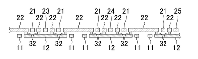
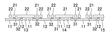
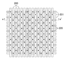
- FIG. 14 is a diagram showing an arrangement example of signal wirings and power supply wirings in a semiconductor device according to a conventional example.
- “200” is a memory core
- “201” is an n-th layer memory core power line
- “202” is an n-th layer signal line
- “203” is an (n + 1) -th layer memory core power line
- “204” is an (n + 1) -th layer signal wiring
- “205” is a wiring interlayer contact.
- mesh-shaped power supply wiring is arranged on the entire chip using the nth layer and the (n + 1) th layer. In each of the nth layer and the (n + 1) th layer, each power supply wiring extends one-dimensionally in a predetermined direction.
- the power supply wiring network spreading like a mesh current is supplied from the peripheral portion toward the central portion. Further, at each point inside the semiconductor integrated circuit, cells located at each point receive current from the power supply wiring network and consume it. Therefore, current is consumed at each point inside the semiconductor integrated circuit, and a voltage drop (voltage drop) in the power supply wiring network increases toward the center of the chip. That is, the voltage on the power supply wiring network is high at the peripheral portion of the semiconductor integrated circuit, and the voltage on the power supply wiring network decreases toward the center of the semiconductor integrated circuit.
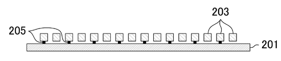
- FIG. 15 and 16 are a top view and a cross-sectional view schematically showing the power supply wiring pattern of the conventional example shown in FIG. 14 in a simplified manner.
- FIG. 17 is a diagram showing an example of voltage drop due to wiring resistance when a power supply voltage is applied to the simplified pattern shown in FIG. 15 to 17, the same components as those in the conventional example shown in FIG. 14 are denoted by the same reference numerals, and redundant description is omitted.
- a power supply voltage is applied from power supply pads 206 and 207 respectively connected to both ends of the (n + 1) -th layer memory core power supply wiring 203.
- the resistance of the (n + 1) th layer memory core power supply wiring (vertical wiring) 203 is higher than the resistance of the nth layer memory core power supply wiring (horizontal wiring) 201, and as a result, (n + 1) )
- a voltage drop occurs sequentially from the peripheral part of the pattern to the center part along the direction in which the power wiring 203 for the layer memory core extends.
- “208” is a region where there is almost no voltage drop
- “209” is a region where a small voltage drop is occurring
- “210” is a region where a large voltage drop is occurring.
- an object of the present invention is to provide a semiconductor device having a power supply wiring structure that can effectively suppress a local voltage drop.
- a semiconductor device includes a first wiring layer and a second wiring layer formed on the upper side or the lower side of the first wiring layer on a semiconductor substrate.
- the first wiring layer includes a plurality of first wiring blocks, each of the first wiring blocks having a first potential and extending in at least two directions, and a second different from the first potential.
- a second wiring having a potential and extending in at least two directions is disposed, and the second wiring layer includes the first wiring block in the pair of first wiring blocks adjacent to each other among the plurality of first wiring blocks.
- the power supply wiring is only in one direction in each wiring layer as in the conventional example. Compared with the case where it extends, the situation where directionality occurs in the voltage drop can be avoided.
- both the first wiring and the second wiring provided in the first wiring layer are two-dimensionally formed as wiring extending in two or more directions.
- the resistance value of each wiring can be reduced as compared with the power supply wiring formed one-dimensionally as wiring extending only in one direction.
- the semiconductor device of the present invention it is possible to realize a power supply wiring structure that can effectively suppress a local voltage drop in the chip.
- the power supply voltage (Vdd) may include a plurality of voltages.
- Vdd the power supply voltage
- a third wiring having a third potential different from the first potential and the second potential may be arranged.
- the arrangement of the first wiring and the second wiring in one first wiring block of the pair of first wiring blocks, and the pair of first wiring blocks may be different. In this way, the resistance difference between the first wiring and the second wiring can be eliminated.
- the second wiring layer may include a plurality of second wiring blocks in which the third wiring and the fourth wiring are respectively arranged.
- the first wiring blocks of the first wiring layer and the second wiring blocks of the second wiring layer may be arranged so as to be shifted from each other.
- each of the third wiring and the fourth wiring may extend in two or more directions. If it does in this way, compared with a prior art example, the above-mentioned effect of the present invention will be exhibited more notably.
- the resistance of the first wiring and the resistance of the third wiring are different, and the resistance of the second wiring and the resistance of the fourth wiring are different. If the resistance is different between the first wiring layer and the second wiring layer, the effects of the present invention described above are more remarkably exhibited as compared with the conventional example.
- the first wiring and the third wiring are electrically connected via a first contact
- the second wiring and the fourth wiring are second contacts. It may be electrically connected via.
- each of the first wiring and the second wiring may be formed in a ring shape. If it does in this way, the above-mentioned effect of the present invention can be acquired certainly.
- each of the first wiring and the second wiring may be formed in a spiral shape. If it does in this way, the above-mentioned effect of the present invention can be acquired certainly.
- each of the first wiring and the second wiring is formed in a ring shape
- each of the first wiring and the second wiring and each of the third wiring and the fourth wiring are electrically connected. Can be arranged easily.
- each wiring can be extended over a wide range without using a contact, so that the resistance of each wiring can be further reduced. Is possible.
- a signal wiring may be arranged between the plurality of first wiring blocks in the first wiring layer.
- the plurality of first wiring blocks may be arranged in a direction in which each side of the semiconductor substrate extends. In this way, a voltage drop in the direction in which each side of the semiconductor substrate extends (chip edge direction) can be suppressed, which is effective for a configuration in which the power supply pads are uniformly arranged on the peripheral edge of the chip.
- the planar shape of the semiconductor substrate is a square shape
- the plurality of first wiring blocks may be arranged in an oblique direction with respect to a direction in which each side of the semiconductor substrate extends.
- the planar shape of the semiconductor substrate may be a square shape, and the plurality of first wiring blocks may be arranged in a direction of 45 degrees with respect to a direction in which each side of the semiconductor substrate extends. In this way, in a general square chip, voltage drop in the direction of 45 degrees with respect to the chip edge direction can be suppressed, which is effective for a configuration in which many power supply pads are arranged at the chip corner portion. is there.
- each of the third wiring and the fourth wiring may be formed in a ring shape. If it does in this way, the above-mentioned effect of the present invention can be acquired certainly.
- the present invention since it is possible to avoid a situation in which the voltage drop has a directionality, a local voltage drop in the semiconductor device can be effectively suppressed, so that the semiconductor device can be stably operated. At the same time, the chip area can be reduced.
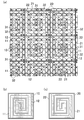
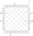
- FIG. 1A is a plan view of a semiconductor device according to the first embodiment of the present invention
- FIG. 1B is a wiring of a lower wiring layer in the semiconductor device according to the first embodiment of the present invention
- FIG. 1C is a diagram showing a wiring block of an upper wiring layer in the semiconductor device according to the first embodiment of the present invention.
- FIG. 2 is a cross-sectional view taken along the line a-a ′ of FIG.
- FIG. 3 is a cross-sectional view taken along line b-b ′ of FIG.
- FIG. 4A is a plan view of a semiconductor device according to a modification of the first embodiment of the present invention
- FIGS. 4B and 4C are related to a modification of the first embodiment of the present invention.
- FIG. 4D is a diagram showing a wiring block of a lower wiring layer in a semiconductor device
- FIGS. 4D and 4E are wiring blocks of an upper wiring layer in a semiconductor device according to a modification of the first embodiment of the present invention.
- FIG. FIG. 5 is a cross-sectional view taken along the line aa ′ in FIG.
- FIG. 5 is a cross-sectional view taken along line b-b ′ of FIG.
- FIG. 7A is a plan view of a semiconductor device according to the second embodiment of the present invention
- FIG. 7B is a wiring of a lower wiring layer in the semiconductor device according to the second embodiment of the present invention.
- FIG. 7C is a diagram showing a wiring block of an upper wiring layer in the semiconductor device according to the second embodiment of the present invention.
- FIG. 8A is a plan view of a semiconductor device according to a modification of the second embodiment of the present invention
- FIGS. 8B and 8C are related to a modification of the second embodiment of the present invention
- FIGS. 8D and 8E are diagrams showing a wiring block of an upper wiring layer in a semiconductor device according to a modification of the second embodiment of the present invention.
- FIGS. FIG. 9 is a plan view showing an example of the arrangement of the wiring block in each embodiment of the present invention (including modifications thereof) in a semiconductor chip.
- FIG. 10 is a plan view showing another example of the arrangement of the wiring block in each embodiment of the present invention (including modifications thereof) in a semiconductor chip.
- FIG. 9 is a plan view showing an example of the arrangement of the wiring block in each embodiment of the present invention (including modifications thereof) in a semiconductor chip.
- FIG. 11 is a cross-sectional view showing a structure example of another wiring layer provided in a layer lower than the first wiring layer and the second wiring layer according to each embodiment of the present invention (including modifications thereof).
- FIG. 12 is a plan view showing an example in which wirings extending in two directions are arranged as power supply wirings and ground wirings of the respective embodiments (including modifications thereof) of the present invention.
- FIG. 13 shows that power supply wirings (or grounding wirings) provided so as to extend in one direction in the lower wiring layer are electrically connected to each other (or grounding wirings) in a wiring block arranged in a staggered manner in the upper wiring layer. It is a top view which shows typically a mode that it connects continuously.
- FIG. 12 is a plan view showing an example in which wirings extending in two directions are arranged as power supply wirings and ground wirings of the respective embodiments (including modifications thereof) of the present invention.
- FIG. 13 shows that power supply wirings (or grounding wirings) provided so as to extend in
- FIG. 14 is a diagram illustrating an arrangement example of signal wirings and power supply wirings in a semiconductor device according to a conventional example.
- FIG. 15 is a top view schematically showing the power supply wiring pattern of the conventional example shown in FIG. 14 in a simplified manner.
- FIG. 16 is a cross-sectional view schematically showing the power supply wiring pattern of the conventional example shown in FIG.
- FIG. 17 is a diagram showing an example of voltage drop due to wiring resistance when a power supply voltage is applied to the simplified pattern shown in FIG.
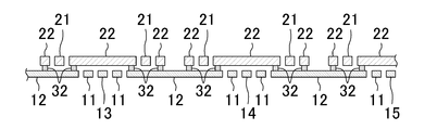
- FIG. 1A is a plan view of the semiconductor device according to the first embodiment
- FIG. 1B is a diagram showing a wiring block of a lower wiring layer in the semiconductor device according to the first embodiment.
- FIG. 1C is a diagram showing a wiring block of the upper wiring layer in the semiconductor device according to the first embodiment.
- 2 is a cross-sectional view taken along the line a-a ′ in FIG. 1A
- FIG. 3 is a cross-sectional view taken along the line b-b ′ in FIG.
- a first wiring layer having a plurality of first wiring blocks 10 (inside the dotted frame in the drawing) is provided above a semiconductor substrate (not shown).
- a second wiring layer having a plurality of second wiring blocks 20 (in the solid line frame in the figure) is provided above the first wiring layer.
- the plurality of first wiring blocks 10 and the plurality of second wiring blocks 20 are arranged in a matrix, and the first wiring blocks 10 and the second wiring blocks 20 are arranged to be shifted from each other. .
- each block is arranged such that the center of the assembly of the four first wiring blocks 10 adjacent in a 2 ⁇ 2 matrix is coincident with the center in one second wiring block 20.
- the blocks are arranged such that the center of the assembly of the four second wiring blocks 20 adjacent in a 2 ⁇ 2 matrix is coincident with the center in one first wiring block 10.
- the arrangement of the blocks is the same in other embodiments and modifications described later.
- each first wiring block 10 is provided with a quadruple ring-shaped wiring in which power supply wiring and ground wiring are alternately arranged.
- a ring-shaped power supply wiring 11, a ground wiring 12, a power supply wiring 11, and a ground wiring 12 are provided in order from the outside.
- a power supply voltage is applied to each power supply wiring 11, and a ground voltage is applied to each ground wiring 12.
- each second wiring block 20 is provided with a quadruple ring-shaped wiring in which power supply wiring and ground wiring are alternately arranged.
- a ring-shaped ground wiring 22, a power wiring 21, a ground wiring 22, and a power wiring 21 are provided in order from the outside.
- a power supply voltage is applied to each power supply wiring 21, and a ground voltage is applied to each ground wiring 22.
- each first wiring block 10 is electrically connected to the power supply wiring 21 of each second wiring block 20 through a first contact 31.
- the ground wiring 12 of each first wiring block 10 is electrically connected to the ground wiring 22 of each second wiring block 20 through a second contact 32.
- the power wirings 11 in the pair of adjacent first wiring blocks 10 are the power wirings of the second wiring block 20.
- the ground wirings 12 in the pair of adjacent first wiring blocks 10 are electrically connected to each other via the ground wiring 22 of the second wiring block 20.
- the power supply wirings 21 in the pair of adjacent second wiring blocks 20 are electrically connected to each other via the power supply wiring 11 of the first wiring block 10 and the ground wiring in the pair of adjacent second wiring blocks 20. 22 are electrically connected through the ground wiring 12 of the first wiring block 10. As a result, a power supply wiring network and a ground wiring network are formed over the entire chip.
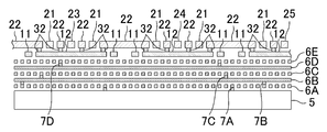
- copper wires having a thickness of, for example, about 0.3 ⁇ m are used as the wires 11 to 15 in the first wiring layer, and each wire 21 to 25 in the second wiring layer is, for example, each wire in the first wiring layer.
- a copper wiring having a thickness of about 1.5 ⁇ m, which is five times the thickness of the wirings 11 to 15 is used.
- the wiring width is, for example, about 10 ⁇ m
- the wiring interval is, for example, about 2.5 ⁇ m. That is, the resistance of each of the wirings 11 to 15 in the first wiring layer is about five times the resistance of each of the wirings 21 to 25 in the second wiring layer.
- both the power supply wiring 11 and the ground wiring 12 provided in the first wiring layer are formed in a ring shape, the power supply wiring and grounding are provided in each wiring layer as in the conventional example. Compared with the case where the wiring extends only in one direction, it is possible to avoid a situation in which directionality occurs in the voltage drop. In particular, when the resistance is different between the first wiring layer and the second wiring layer as in the present embodiment, the above-described effect is remarkable as compared with the conventional example.
- both the power supply wiring 11 and the ground wiring 12 provided in the first wiring layer are two-dimensionally formed as wirings extending in two or more directions.
- the resistance value per unit area in each block can be reduced by about 20% as compared with the power supply wiring and ground wiring formed one-dimensionally as wiring extending only in the direction.
- the present embodiment it is possible to realize a power supply wiring structure that can effectively suppress a local voltage drop in the chip.
- a local voltage drop in the semiconductor device can be effectively suppressed, the semiconductor device can be stably operated and the chip area can be reduced.
- both the power supply wiring 21 and the ground wiring 22 provided in the second wiring layer are formed in a ring shape, the effects of the present embodiment described above can be obtained compared to the conventional example. It is more prominent.
- each of the first wiring blocks 10 and each of the second wiring blocks 20 is provided with a ring-shaped wiring having a quadruple structure. Instead, a ring-shaped wiring having a structure of double, triple, or five or more is provided. May be. Furthermore, the structure of the ring-shaped wiring provided in each first wiring block 10 and each second wiring block 20 may be different from each other.
- the signal wirings 13 to 15 of the first wiring layer are respectively connected to the substrate or wiring layer below the first wiring layer or the upper side of the first wiring layer.
- a contact for electrical connection with the second wiring layer or the pad may be formed.
- each of the signal wirings 23 to 25 of the second wiring layer is electrically connected to a substrate below the second wiring layer, a wiring layer such as the first wiring layer, or a pad above the second wiring layer. For this purpose, a contact may be formed.
- the signal wirings 13 to 15 are arranged between the plurality of first wiring blocks 10 in the first wiring layer, and between the plurality of second wiring blocks 20 in the second wiring layer.
- the signal wirings 23 to 25 are disposed in However, instead of this, the signal wirings 13 to 15 and 23 to 25 may not be arranged. In other words, only the power supply wiring 11 and the ground wiring 12 may be arranged in the first wiring layer, and only the power supply wiring 21 and the ground wiring 22 may be arranged in the second wiring layer. In this way, since the power supply wiring and the ground wiring can be provided without waste in each wiring layer, the resistance values of the power supply wiring and the ground wiring are compared with the case where the signal wirings 13 to 15 and 23 to 25 are arranged. Can be further reduced by about 5%.
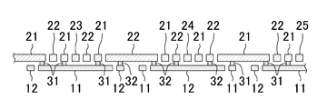
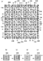
- FIG. 4A is a plan view of a semiconductor device according to a modification of the first embodiment
- FIGS. 4B and 4C are lower side views of the semiconductor device according to the modification of the first embodiment
- FIGS. 4D and 4E are diagrams showing a wiring block of an upper wiring layer in a semiconductor device according to a modification of the first embodiment.
- FIG. FIG. 5 is a cross-sectional view taken along the line a-a ′ in FIG. 4A
- FIG. 6 is a cross-sectional view taken along the line b-b ′ in FIG.
- FIGS. 4A to 4E, 5 and 6 the same components as those in the first embodiment shown in FIGS. 1A to 1C, 2 and 3 are the same. A duplicate description is omitted by attaching a reference numeral.
- the first difference of the present modification from the first embodiment is that, as shown in FIGS. 4A to 4C, the arrangement order of the power supply wiring 11 and the ground wiring 12 as the first wiring block 10 is as follows.
- the two types of first wiring blocks 10A and 10B differing from each other are arranged so as to be alternately adjacent to each other.
- the first wiring block 10A is provided with a ring-shaped power wiring 11, a ground wiring 12, a power wiring 11 and a ground wiring 12 each having a quadruple structure in order from the outside.
- the first wiring block 10B is provided with a ring-shaped wiring having a quadruple structure in which the ring-shaped ground wiring 12, the power wiring 11, the ground wiring 12, and the power wiring 11 are arranged in order from the outside.
- a second point that the present modification is different from the first embodiment is that, as shown in FIGS. 4A, 4D, and 4E, as the second wiring block 20, the power wiring 21 and That is, two types of second wiring blocks 20A and 20B having different arrangement orders of the ground wirings 22 are arranged so as to be alternately adjacent to each other.
- the second wiring block 20A is provided with a ring-shaped power wiring 21, a ground wiring 22, a power wiring 21 and a ground wiring 22 each having a quadruple structure in order from the outside.
- the second wiring block 20B is provided with a ring-shaped wiring having a quadruple structure in which the ring-shaped ground wiring 22, the power wiring 21, the ground wiring 22, and the power wiring 21 are arranged in order from the outside.
- the following effects can be obtained in addition to the same effects as those of the first embodiment. That is, since the arrangement order of the power supply wiring 11 and the ground wiring 12 is reversed between the adjacent first wiring blocks 10A and 10B, the resistance difference between the power supply wiring 11 and the ground wiring 12 can be eliminated. it can. Further, since the arrangement order of the power supply wiring 21 and the ground wiring 22 is reversed between the adjacent second wiring blocks 20A and 20B, the resistance difference between the power supply wiring 21 and the ground wiring 22 can be eliminated. it can.
- FIG. 7A is a plan view of the semiconductor device according to the second embodiment
- FIG. 7B is a diagram illustrating a wiring block of a lower wiring layer in the semiconductor device according to the second embodiment.
- FIG. 7C is a diagram showing a wiring block of the upper wiring layer in the semiconductor device according to the second embodiment.
- 7 (a) to 7 (c) the same components as those in the first embodiment shown in FIGS. 1 (a) to 1 (c) are denoted by the same reference numerals, and redundant description is omitted. .
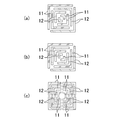
- each first wiring block 10 includes a power wiring 11 and a ground wiring each having a spiral shape. 12 is provided one by one, and each second wiring block 20 is provided with one power wiring 21 and one ground wiring 22 each having a spiral shape.
- each of the power supply wiring 11 and the ground wiring 12 and the power supply wiring 21 and the ground wiring 22 is formed in a ring shape, each of the power supply wiring 11 and the ground wiring 12 and each of the power supply wiring 21 and the ground wiring 22. Can be easily arranged. Further, compared to the case where the power supply wiring 11 and the ground wiring 12 and the power supply wiring 21 and the ground wiring 22 are respectively formed in a ring shape, the power supply wiring 11 and the ground wiring 12, and the power supply wiring 21 and the ground wiring 22 are respectively spirally connected. Since each wiring can be extended over a wide range without using the contacts 31 and 32, the resistance of each wiring can be further reduced.
- the arrangement order of the power supply wiring 11 and the ground wiring 12 in each first wiring block 10 is changed, and the arrangement order of the power supply wiring 21 and the ground wiring 22 in each second wiring block 20 is changed. Also good.
- the number of turns of each of the power wiring 11, the ground wiring 12, the power wiring 21 and the ground wiring 22, which are spiral wirings, is not particularly limited. Furthermore, the structure of the spiral wiring provided in each first wiring block 10 and each second wiring block 20 may be different from each other.
- each of the first wiring blocks 10 and each of the second wiring blocks 20 is provided with a spiral wiring.
- the power wiring 11 is provided in each of the first wiring blocks 10.
- a ring-shaped wiring similar to that of the first embodiment is provided as the ground wiring 12, and a spiral wiring similar to that of the present embodiment is provided as the power wiring 21 and the ground wiring 22 in each second wiring block 20.
- each first wiring block 10 is provided with a spiral wiring similar to that of the present embodiment as the power supply wiring 11 and the ground wiring 12, and each second wiring block 20 is provided with a power wiring 21 and a ground wiring 22 as the first wiring.
- a ring-shaped wiring similar to that of the first embodiment may be provided.
- the signal wiring is arranged between the first wiring blocks 10A and 10B in the first wiring layer, and the signal wiring is arranged between the second wiring blocks 20A and 20B in the second wiring layer. May be.
- FIG. 8A is a plan view of a semiconductor device according to a modification of the second embodiment
- FIGS. 8B and 8C are lower side views of the semiconductor device according to the modification of the second embodiment
- FIGS. 8D and 8E are diagrams showing a wiring block of an upper wiring layer in a semiconductor device according to a modification of the second embodiment.
- a first difference of the present modification from the second embodiment is that, as shown in FIGS. 8A to 8C, the first wiring block 10 includes a power wiring 11 that is a spiral wiring and That is, two types of first wiring blocks 10A and 10B having different arrangement methods of the ground wiring 12 are arranged so as to be alternately adjacent to each other.
- a second point that the present modification is different from the second embodiment is that, as shown in FIGS. 8A, 8D, and 8E, the second wiring block 20 is a spiral wiring. That is, two types of second wiring blocks 20A and 20B having different arrangements of the power supply wiring 21 and the ground wiring 22 are arranged so as to be alternately adjacent to each other.
- the following effects can be obtained in addition to the same effects as those of the second embodiment. That is, since the arrangement of the power supply wiring 11 and the ground wiring 12 is changed between the adjacent first wiring blocks 10A and 10B, the resistance difference between the power supply wiring 11 and the ground wiring 12 can be eliminated. it can. In addition, since the arrangement of the power supply wiring 21 and the ground wiring 22 is changed between the adjacent second wiring blocks 20A and 20B, the resistance difference between the power supply wiring 21 and the ground wiring 22 can be eliminated. it can.
- the power supply voltage may include a plurality of voltages.
- two or more types of power supply lines to which two or more different types of power supply voltages are applied may be provided in each wiring block of each wiring layer.
- the size of each wiring block is not particularly limited.
- it may be formed with a size of about 100 ⁇ m ⁇ to about 400 ⁇ m ⁇ .
- the contact resistance is high, it is desirable to make the block size somewhat large in order to reduce the influence of the contact resistance.
- the block size may be small as long as a plurality of ring-shaped wirings or spiral wirings can be arranged.
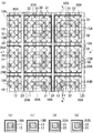
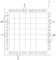
- FIG. 9 is a plan view showing an example of the arrangement of the wiring blocks (specifically, the second wiring block of the second wiring layer, which is the upper wiring layer) of each of the embodiments in the semiconductor chip.
- a plurality of pads 2 are arranged on the peripheral portion of the rectangular semiconductor chip 1
- a plurality of second wiring blocks 20 are located inside the semiconductor chip 1 (that is, inside the arrangement area of the pads 2).
- semiconductor substrate are arranged in the extending direction. That is, each second wiring block 20 is arranged along the same direction as the chip edge direction. In this way, a voltage drop in the chip edge direction can be suppressed, which is effective for a configuration in which the power supply pads are uniformly arranged on the peripheral edge of the chip.
- FIG. 10 is a plan view showing another example of the arrangement in the semiconductor chip of the wiring block of each of the embodiments described above (specifically, the second wiring block of the second wiring layer which is the upper wiring layer).
- a plurality of pads 2 are arranged at the peripheral edge of the square semiconductor chip 1, and a plurality of second wiring blocks 20 are located inside the semiconductor chip 1 (that is, inside the arrangement area of the pads 2).
- the semiconductor substrate is arranged in a direction of 45 degrees with respect to the diagonal direction of the semiconductor substrate, that is, the chip edge direction. In this way, a voltage drop in the 45-degree direction (chip diagonal direction) with respect to the chip edge direction can be suppressed, which is effective for a configuration in which many power supply pads are arranged at the chip corner portion.
- FIG. 10 shows the case where the semiconductor chip 1 has a square shape. However, when the semiconductor chip 1 has a rectangular shape, a plurality of second wiring blocks 20 are connected to the semiconductor chip 1 (that is, the semiconductor substrate). What is necessary is just to arrange in a diagonal direction with respect to a diagonal direction, ie, a chip edge direction.
- the first wiring block 10 of the first wiring layer that is the lower wiring layer may also be arranged along the same direction as the chip edge direction. Needless to say, they may be arranged obliquely with respect to the chip edge direction.
- the second wiring layer (upper wiring layer) on which the second wiring block is provided is the same chip uppermost layer as the pad.
- the second wiring layer is a wiring immediately below the pad. It may be a layer, or another wiring layer may be interposed between the second wiring layer and the uppermost layer of the chip.
- FIG. 11 is a cross-sectional view showing an example of the structure of another wiring layer provided below the first wiring layer and the second wiring layer in each of the embodiments.
- the first embodiment shown in FIGS. 1 (a) to 1 (c), FIGS. 2 and 3, and the first embodiment shown in FIGS. 4 (a) to (e), FIG. 5 and FIG. The same components as those of the modification of the embodiment, the second embodiment shown in FIGS. 7A to 7C, or the modification of the second embodiment shown in FIGS.
- the description which overlaps is abbreviate
- the wiring layers 6A to 6E are formed on the semiconductor substrate 5 on which transistors and the like are formed. Further, the semiconductor substrate 5 and the wiring layer 6A are electrically connected by a contact 7A, and the wiring layer 6A and the wiring layer 6B are electrically connected by a contact 7B, and the wiring layer 6B and the wiring layer 6C are connected to each other. Are electrically connected by a contact 7C, and the wiring layer 6D and the wiring layer 6E are electrically connected by a contact 7D.
- copper wiring is used as each of the wirings 11 to 15 of the first wiring layer and each of the wirings 21 to 25 of the second wiring layer, but instead, copper wiring is used for the first wiring layer.
- copper wiring is used for the first wiring layer.
- aluminum wiring may be used for the second wiring layer.
- the aluminum wiring used for the second wiring layer is an aluminum wiring formed by wire bonding, and by applying the power supply wiring structure of each of the embodiments to at least the second wiring layer, As a similar effect, it is possible to realize a low-resistance power supply wiring network and a ground wiring network in which no directionality occurs in the voltage drop.
- the shape of the wiring blocks 10 and 20 is set to a square (for example, a square), but the shape of the wiring blocks 10 and 20 is not particularly limited. Even when any shape such as a triangle, hexagon, octagon, or the like is adopted as the shape of the wiring blocks 10 and 20, by providing ring-shaped wiring or spiral wiring according to each block shape, As an effect similar to that of the embodiment, it is possible to realize a low-resistance power supply wiring network and a ground wiring network in which no directionality occurs in the voltage drop. Further, as the shapes of the wiring blocks 10 and 20, a plurality of shapes may be used simultaneously, or the shapes of the wiring blocks 10 and 20 may be different from each other.
- the ring wiring or the spiral wiring is arranged as the power wiring 11 and the ground wiring 12 and the power wiring 21 and the ground wiring 22 arranged in the wiring blocks 10 and 20, but the power wiring 11
- the wiring that can be arranged as the power wiring 21 and the ground wiring 22 is not particularly limited as long as the wiring extends in at least two directions.
- FIGS. 12A to 12C are plan views showing examples in which wiring extending in two directions is arranged as the power supply wiring 11 and the ground wiring 12, respectively.
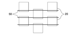
- a plurality of wiring blocks 10 are arranged in a matrix in the first wiring layer, which is a lower wiring layer, and a plurality of wiring blocks 20 are arranged in a matrix in the second wiring layer, which is an upper wiring layer.
- a plurality of wiring blocks 20 are arranged in a staggered pattern in the second wiring layer that is the upper wiring layer, and the power wiring is provided in the first wiring layer that is the lower wiring layer.
- (Or ground wiring) 50 is provided so as to extend in one direction, and power wirings (or ground wirings) in partially adjacent wiring blocks 20 are electrically connected by power wiring (or ground wiring) 50. Also good.
- a wiring block in the first wiring layer which is the lower wiring layer it is not necessary to provide a wiring block in the first wiring layer which is the lower wiring layer.
- a plurality of wiring blocks 10 are arranged in a staggered pattern in the first wiring layer that is the lower wiring layer, and the power supply wiring (or ground wiring) is extended in one direction in the second wiring layer that is the upper wiring layer.
- the power supply wires (or the ground wires) in the partially adjacent wiring blocks 10 may be electrically connected to each other by the power supply wires (or the ground wires) extending in the one direction. That is, the wiring block may not be provided in the second wiring layer that is the upper wiring layer.
- the present invention can effectively suppress a local voltage drop in a semiconductor device, and can thereby operate the semiconductor device stably and reduce the chip area, which is useful. It is.
Landscapes
- Design And Manufacture Of Integrated Circuits (AREA)
- Semiconductor Integrated Circuits (AREA)
- Internal Circuitry In Semiconductor Integrated Circuit Devices (AREA)
Priority Applications (1)
| Application Number | Priority Date | Filing Date | Title |
|---|---|---|---|
| US13/289,683 US8710667B2 (en) | 2009-05-27 | 2011-11-04 | Semiconductor device |
Applications Claiming Priority (2)
| Application Number | Priority Date | Filing Date | Title |
|---|---|---|---|
| JP2009-127377 | 2009-05-27 | ||
| JP2009127377A JP5190414B2 (ja) | 2009-05-27 | 2009-05-27 | 半導体装置 |
Related Child Applications (1)
| Application Number | Title | Priority Date | Filing Date |
|---|---|---|---|
| US13/289,683 Continuation US8710667B2 (en) | 2009-05-27 | 2011-11-04 | Semiconductor device |
Publications (1)
| Publication Number | Publication Date |
|---|---|
| WO2010137098A1 true WO2010137098A1 (ja) | 2010-12-02 |
Family
ID=43222242
Family Applications (1)
| Application Number | Title | Priority Date | Filing Date |
|---|---|---|---|
| PCT/JP2009/007142 Ceased WO2010137098A1 (ja) | 2009-05-27 | 2009-12-22 | 半導体装置 |
Country Status (3)
| Country | Link |
|---|---|
| US (1) | US8710667B2 (enExample) |
| JP (1) | JP5190414B2 (enExample) |
| WO (1) | WO2010137098A1 (enExample) |
Families Citing this family (6)
| Publication number | Priority date | Publication date | Assignee | Title |
|---|---|---|---|---|
| US8846449B2 (en) | 2011-05-17 | 2014-09-30 | Panasonic Corporation | Three-dimensional integrated circuit, processor, semiconductor chip, and manufacturing method of three-dimensional integrated circuit |
| TWI475939B (zh) * | 2013-10-15 | 2015-03-01 | 緯創資通股份有限公司 | 散熱式鏤空之形成方法及形成之散熱式鏤空結構 |
| JP2015207730A (ja) * | 2014-04-23 | 2015-11-19 | マイクロン テクノロジー, インク. | 半導体装置 |
| JP6295863B2 (ja) * | 2014-07-16 | 2018-03-20 | 富士通株式会社 | 電子部品、電子装置及び電子装置の製造方法 |
| US9287208B1 (en) | 2014-10-27 | 2016-03-15 | Intel Corporation | Architecture for on-die interconnect |
| CN113224047A (zh) * | 2020-01-21 | 2021-08-06 | 扬智科技股份有限公司 | 集成电路结构 |
Citations (3)
| Publication number | Priority date | Publication date | Assignee | Title |
|---|---|---|---|---|
| JP2004273844A (ja) * | 2003-03-10 | 2004-09-30 | Fujitsu Ltd | 半導体集積回路 |
| JP2008270319A (ja) * | 2007-04-17 | 2008-11-06 | Toshiba Corp | 半導体装置 |
| JP2009054702A (ja) * | 2007-08-24 | 2009-03-12 | Panasonic Corp | 半導体集積回路 |
Family Cites Families (5)
| Publication number | Priority date | Publication date | Assignee | Title |
|---|---|---|---|---|
| US6308307B1 (en) * | 1998-01-29 | 2001-10-23 | Texas Instruments Incorporated | Method for power routing and distribution in an integrated circuit with multiple interconnect layers |
| JP3692254B2 (ja) | 1999-03-25 | 2005-09-07 | 京セラ株式会社 | 多層配線基板 |
| US6483714B1 (en) | 1999-02-24 | 2002-11-19 | Kyocera Corporation | Multilayered wiring board |
| JP2005332903A (ja) | 2004-05-19 | 2005-12-02 | Matsushita Electric Ind Co Ltd | 半導体装置 |
| JP4539916B2 (ja) | 2005-01-19 | 2010-09-08 | ルネサスエレクトロニクス株式会社 | 半導体集積回路、半導体集積回路の設計方法、及び半導体集積回路の設計用プログラム |
-
2009
- 2009-05-27 JP JP2009127377A patent/JP5190414B2/ja not_active Expired - Fee Related
- 2009-12-22 WO PCT/JP2009/007142 patent/WO2010137098A1/ja not_active Ceased
-
2011
- 2011-11-04 US US13/289,683 patent/US8710667B2/en active Active
Patent Citations (3)
| Publication number | Priority date | Publication date | Assignee | Title |
|---|---|---|---|---|
| JP2004273844A (ja) * | 2003-03-10 | 2004-09-30 | Fujitsu Ltd | 半導体集積回路 |
| JP2008270319A (ja) * | 2007-04-17 | 2008-11-06 | Toshiba Corp | 半導体装置 |
| JP2009054702A (ja) * | 2007-08-24 | 2009-03-12 | Panasonic Corp | 半導体集積回路 |
Also Published As
| Publication number | Publication date |
|---|---|
| JP5190414B2 (ja) | 2013-04-24 |
| US20120112354A1 (en) | 2012-05-10 |
| JP2010278104A (ja) | 2010-12-09 |
| US8710667B2 (en) | 2014-04-29 |
Similar Documents
| Publication | Publication Date | Title |
|---|---|---|
| US7821038B2 (en) | Power and ground routing of integrated circuit devices with improved IR drop and chip performance | |
| US10002833B2 (en) | Power and ground routing of integrated circuit devices with improved IR drop and chip performance | |
| JP5190414B2 (ja) | 半導体装置 | |
| US10403572B2 (en) | Semiconductor device and semiconductor package including the same | |
| US20120007255A1 (en) | Semiconductor device | |
| JP2009054702A (ja) | 半導体集積回路 | |
| US10037939B2 (en) | Semiconductor apparatus | |
| JP2017174971A (ja) | 半導体集積回路チップ及び半導体集積回路ウェーハ | |
| JP5131814B2 (ja) | 半導体装置 | |
| JP2008053358A (ja) | 半導体装置及び半導体パッケージ | |
| JP2006019692A (ja) | 半導体装置 | |
| JP5138260B2 (ja) | チップ型電子部品 | |
| JP2010087336A (ja) | 半導体集積回路 | |
| WO2018105258A1 (ja) | 半導体装置 | |
| CN104937711B (zh) | 半导体集成电路 | |
| JP2009194022A (ja) | チップサイズパッケージ及び半導体装置 | |
| CN101479848A (zh) | 供电网络 | |
| JP2006202866A (ja) | 半導体装置 | |
| JP4343124B2 (ja) | 半導体装置 | |
| JP5640438B2 (ja) | 半導体装置 | |
| KR20180048220A (ko) | 반도체 장치 및 이를 포함한 반도체 패키지 | |
| JP5168872B2 (ja) | 半導体集積回路 | |
| JP2005327987A (ja) | 半導体装置 | |
| US12362305B2 (en) | Semiconductor structure | |
| CN101740533B (zh) | 集成电路 |
Legal Events
| Date | Code | Title | Description |
|---|---|---|---|
| 121 | Ep: the epo has been informed by wipo that ep was designated in this application |
Ref document number: 09845165 Country of ref document: EP Kind code of ref document: A1 |
|
| NENP | Non-entry into the national phase |
Ref country code: DE |
|
| 122 | Ep: pct application non-entry in european phase |
Ref document number: 09845165 Country of ref document: EP Kind code of ref document: A1 |