WO2010125795A1 - Moule et procédé de fabrication de celui-ci - Google Patents
Moule et procédé de fabrication de celui-ci Download PDFInfo
- Publication number
- WO2010125795A1 WO2010125795A1 PCT/JP2010/002989 JP2010002989W WO2010125795A1 WO 2010125795 A1 WO2010125795 A1 WO 2010125795A1 JP 2010002989 W JP2010002989 W JP 2010002989W WO 2010125795 A1 WO2010125795 A1 WO 2010125795A1
- Authority
- WO
- WIPO (PCT)
- Prior art keywords
- layer
- mold
- roll
- curable resin
- flexible
- Prior art date
Links
Images


Classifications
-
- G—PHYSICS
- G02—OPTICS
- G02B—OPTICAL ELEMENTS, SYSTEMS OR APPARATUS
- G02B1/00—Optical elements characterised by the material of which they are made; Optical coatings for optical elements
- G02B1/10—Optical coatings produced by application to, or surface treatment of, optical elements
- G02B1/11—Anti-reflection coatings
- G02B1/118—Anti-reflection coatings having sub-optical wavelength surface structures designed to provide an enhanced transmittance, e.g. moth-eye structures
-
- B—PERFORMING OPERATIONS; TRANSPORTING
- B29—WORKING OF PLASTICS; WORKING OF SUBSTANCES IN A PLASTIC STATE IN GENERAL
- B29C—SHAPING OR JOINING OF PLASTICS; SHAPING OF MATERIAL IN A PLASTIC STATE, NOT OTHERWISE PROVIDED FOR; AFTER-TREATMENT OF THE SHAPED PRODUCTS, e.g. REPAIRING
- B29C33/00—Moulds or cores; Details thereof or accessories therefor
- B29C33/38—Moulds or cores; Details thereof or accessories therefor characterised by the material or the manufacturing process
-
- B—PERFORMING OPERATIONS; TRANSPORTING
- B29—WORKING OF PLASTICS; WORKING OF SUBSTANCES IN A PLASTIC STATE IN GENERAL
- B29C—SHAPING OR JOINING OF PLASTICS; SHAPING OF MATERIAL IN A PLASTIC STATE, NOT OTHERWISE PROVIDED FOR; AFTER-TREATMENT OF THE SHAPED PRODUCTS, e.g. REPAIRING
- B29C33/00—Moulds or cores; Details thereof or accessories therefor
- B29C33/42—Moulds or cores; Details thereof or accessories therefor characterised by the shape of the moulding surface, e.g. ribs or grooves
- B29C33/424—Moulding surfaces provided with means for marking or patterning
-
- C—CHEMISTRY; METALLURGY
- C25—ELECTROLYTIC OR ELECTROPHORETIC PROCESSES; APPARATUS THEREFOR
- C25D—PROCESSES FOR THE ELECTROLYTIC OR ELECTROPHORETIC PRODUCTION OF COATINGS; ELECTROFORMING; APPARATUS THEREFOR
- C25D11/00—Electrolytic coating by surface reaction, i.e. forming conversion layers
- C25D11/02—Anodisation
- C25D11/04—Anodisation of aluminium or alloys based thereon
- C25D11/045—Anodisation of aluminium or alloys based thereon for forming AAO templates
-
- C—CHEMISTRY; METALLURGY
- C25—ELECTROLYTIC OR ELECTROPHORETIC PROCESSES; APPARATUS THEREFOR
- C25D—PROCESSES FOR THE ELECTROLYTIC OR ELECTROPHORETIC PRODUCTION OF COATINGS; ELECTROFORMING; APPARATUS THEREFOR
- C25D11/00—Electrolytic coating by surface reaction, i.e. forming conversion layers
- C25D11/02—Anodisation
- C25D11/04—Anodisation of aluminium or alloys based thereon
- C25D11/12—Anodising more than once, e.g. in different baths
-
- C—CHEMISTRY; METALLURGY
- C25—ELECTROLYTIC OR ELECTROPHORETIC PROCESSES; APPARATUS THEREFOR
- C25D—PROCESSES FOR THE ELECTROLYTIC OR ELECTROPHORETIC PRODUCTION OF COATINGS; ELECTROFORMING; APPARATUS THEREFOR
- C25D11/00—Electrolytic coating by surface reaction, i.e. forming conversion layers
- C25D11/02—Anodisation
- C25D11/04—Anodisation of aluminium or alloys based thereon
- C25D11/18—After-treatment, e.g. pore-sealing
- C25D11/24—Chemical after-treatment
-
- B—PERFORMING OPERATIONS; TRANSPORTING
- B29—WORKING OF PLASTICS; WORKING OF SUBSTANCES IN A PLASTIC STATE IN GENERAL
- B29K—INDEXING SCHEME ASSOCIATED WITH SUBCLASSES B29B, B29C OR B29D, RELATING TO MOULDING MATERIALS OR TO MATERIALS FOR MOULDS, REINFORCEMENTS, FILLERS OR PREFORMED PARTS, e.g. INSERTS
- B29K2995/00—Properties of moulding materials, reinforcements, fillers, preformed parts or moulds
- B29K2995/0018—Properties of moulding materials, reinforcements, fillers, preformed parts or moulds having particular optical properties, e.g. fluorescent or phosphorescent
- B29K2995/0024—Matt surface
-
- G—PHYSICS
- G02—OPTICS
- G02B—OPTICAL ELEMENTS, SYSTEMS OR APPARATUS
- G02B5/00—Optical elements other than lenses
- G02B5/30—Polarising elements
- G02B5/3025—Polarisers, i.e. arrangements capable of producing a definite output polarisation state from an unpolarised input state
- G02B5/3033—Polarisers, i.e. arrangements capable of producing a definite output polarisation state from an unpolarised input state in the form of a thin sheet or foil, e.g. Polaroid
Definitions
- the present invention relates to a mold and a method for manufacturing the mold.
- the “mold” here includes molds used in various processing methods (stamping and casting), and is sometimes referred to as a stamper. It can also be used for printing (including nanoprinting).
- An optical element such as a display device or a camera lens used for a television or a mobile phone is usually provided with an antireflection technique in order to reduce surface reflection and increase light transmission.
- an antireflection technique in order to reduce surface reflection and increase light transmission. For example, when light passes through the interface of a medium with a different refractive index, such as when light enters the interface between air and glass, the amount of transmitted light is reduced due to Fresnel reflection, and visibility is reduced. is there.
- This method utilizes the principle of the so-called moth-eye structure, and the refractive index for light incident on the substrate is calculated from the refractive index of the incident medium along the depth direction of the irregularities. In this way, the reflection in the wavelength region where the reflection is to be prevented is suppressed.
- the moth-eye structure has an advantage that it can exhibit an antireflection effect with a small incident angle dependency over a wide wavelength range, can be applied to many materials, and can form an uneven pattern directly on a substrate. As a result, a low-cost and high-performance antireflection film (or antireflection surface) can be provided.
- Patent Documents 2 to 4 As a method for producing a moth-eye structure, a method using an anodized porous alumina layer obtained by anodizing aluminum is attracting attention (Patent Documents 2 to 4).
- anodized porous alumina layer obtained by anodizing aluminum will be briefly described.
- a method for producing a porous structure using anodization has attracted attention as a simple method capable of forming regularly ordered nano-sized cylindrical pores (fine concave portions).
- an acidic or alkaline electrolyte such as sulfuric acid, oxalic acid, or phosphoric acid
- a voltage is applied using the aluminum substrate as an anode
- oxidation and dissolution proceed simultaneously on the surface of the aluminum substrate.
- An oxide film having pores can be formed. These cylindrical pores are oriented perpendicular to the oxide film and exhibit self-organized regularity under certain conditions (voltage, type of electrolyte, temperature, etc.). Is expected.
- the porous alumina layer formed under specific conditions takes an array in which almost regular hexagonal cells are two-dimensionally filled with the highest density when viewed from the direction perpendicular to the film surface.
- Each cell has a pore in the center, and the arrangement of the pores has periodicity.
- the cell is formed as a result of local dissolution and growth of the film, and dissolution and growth of the film proceed simultaneously at the bottom of the pores called a barrier layer.
- the cell size that is, the distance between adjacent pores (center-to-center distance) corresponds to approximately twice the thickness of the barrier layer and is approximately proportional to the voltage during anodization.
- the diameter of the pores depends on the type, concentration, temperature, etc.
- the pores of such porous alumina have an arrangement with high regularity (having periodicity) under a specific condition, an arrangement with irregularity to some extent or an irregularity (having no periodicity) depending on the conditions. ).
- Patent Document 2 discloses a method of forming an antireflection film (antireflection surface) using a stamper having an anodized porous alumina film on the surface.
- Patent Document 3 discloses a technique for forming a tapered concave portion in which the pore diameter continuously changes by repeating anodization of aluminum and pore diameter enlargement processing.
- Patent Document 4 a technique for forming an antireflection film using an alumina layer in which fine concave portions have stepped side surfaces.
- an antireflection film (antireflection surface) is provided by providing a concavo-convex structure (macro structure) larger than the moth eye structure in addition to the moth eye structure (micro structure). ) Can be given an anti-glare (anti-glare) function.
- the two-dimensional size of the projections that form the projections and depressions that exhibit the antiglare function is 1 ⁇ m or more and less than 100 ⁇ m.
- a mold for forming a moth-eye structure on the surface (hereinafter referred to as “moth-eye mold”) can be easily manufactured.
- the surface of an anodized aluminum film is used as it is as a mold, the effect of reducing the manufacturing cost is great.
- the surface structure of the moth-eye mold that can form the moth-eye structure is referred to as an “inverted moth-eye structure”.
- Patent Document 5 describes a method for manufacturing a roll-shaped resin mold used for manufacturing a lens sheet, which will be described below.
- a metal cutting die having a shape opposite to that of a lens is pressed against a film-like base material provided with a silicone resin to produce a film-like die having a lens shape (first transfer).
- a thermosetting resin is applied between the film mold and the iron core cylinder while the film mold is wound around the iron core cylinder, and the resin is thermoset. Thereafter, the film mold is peeled off to obtain a roll-shaped resin mold having a shape opposite to that of the lens (second transfer).
- the present inventor studied the production of a flexible moth-eye mold that can be deformed into a roll shape.
- An attempt to produce a moth-eye mold using an aluminum layer formed on the surface of a flexible polymer film resulted in a problem that sufficient adhesion between the aluminum layer and the polymer film could not be obtained. .
- the present invention has been made to solve the above problems, and its main object is to provide a method for easily producing a flexible moth-eye mold.
- the flexible mold of the present invention is a polymer film having flexibility, a curable resin layer formed on the surface of the polymer film, and a porous alumina layer formed on the curable resin layer. And a porous alumina layer having an inverted moth-eye structure on the surface having a plurality of recesses having a two-dimensional size of 10 nm or more and less than 500 nm when viewed from the normal direction of the surface.
- the curable resin layer includes an acrylic resin.
- an inorganic underlayer is formed between the curable resin layer and the porous alumina layer.
- the inorganic underlayer includes SiO 2 .
- the inorganic underlayer has a thickness of 50 nm to 300 nm.
- a buffer layer containing aluminum is formed between the inorganic underlayer and the porous alumina layer.
- the curable resin layer contains silica.
- the surface of the curable resin layer has a convex portion having a two-dimensional size of 1 ⁇ m or more and less than 100 ⁇ m.
- a periodic uneven structure is formed on the surface of the curable resin layer.
- the roll-shaped mold of the present invention includes a flexible mold having the above-described configuration and a roll-shaped substrate, and the flexible mold is fixed on the outer peripheral surface of the roll-shaped substrate.
- the flexible mold is arranged such that a gap is provided between one end and the other end.
- the method for forming the antireflection structure of the present invention includes the step of preparing the roll-shaped mold and the polarizing plate, and the polarizing axis of the polarizing plate and the circumferential direction of the roll-shaped mold are parallel. And moving the polarizing plate relative to the roll mold to form the moth-eye structure on the polarizing plate.
- the polarizing plate is rectangular, and the circumference of the roll-shaped mold is longer than the long side of the polarizing plate.
- the method for producing a flexible mold according to the present invention is a flexible mold having a reversed moth-eye structure on the surface, which has a plurality of recesses having a two-dimensional size of 10 nm or more and less than 500 nm when viewed from the normal direction of the surface.
- a manufacturing method comprising: (a) a flexible polymer film; a curable resin layer formed on a surface of the polymer film; and an aluminum layer formed on the curable resin layer.
- step (b) forming a porous alumina layer having a plurality of fine recesses by partially anodizing the aluminum layer, and (c) the step (b) ), The step of bringing the porous alumina layer into contact with an etching solution to enlarge the plurality of fine recesses of the porous alumina layer, and (d) the step (c) After, by further anodization, including the steps of growing a plurality of minute recesses.
- the steps (c) and (d) are further performed after the step (d).
- the method for producing a roll-shaped mold of the present invention comprises (e) a step of preparing a roll-shaped substrate and a flexible mold having the above-described configuration, and (f) the roll-shaped after the step (e). Fixing the flexible mold to the outer peripheral surface of the substrate.
- the polymer film is knurled at the end.
- a method for easily producing a flexible moth-eye mold is provided.
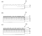
- FIG. (A)-(e) is typical sectional drawing for demonstrating the manufacturing method of the type
- (A) is typical sectional drawing of the mold base material 10 used for the manufacturing method of the type
- (b) is the mold 100 for moth eyes manufactured using the mold base material 10.
- FIG. FIG. (A) is typical sectional drawing of the mold base 10a used for the manufacturing method of the type
- FIG. (A) is typical sectional drawing of the mold base material 10b used for the manufacturing method of the type
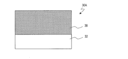
- FIG. 5 is a schematic cross-sectional view of a mold base 30A of Comparative Example 1.
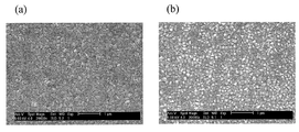
- FIG. 3 is a diagram showing an SEM image of the surface of the porous alumina layer of the mold substrate 10 of Example 1.
- FIG. 10 is a schematic cross-sectional view of a mold substrate 30B of Comparative Example 2.
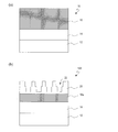
- FIG. (A) And (b) is a figure which shows the SEM image of the surface of the aluminum layer of the type
- (a) is a SEM image immediately after film-forming of an aluminum layer
- (b) Indicates an SEM image after immersion in an aqueous phosphoric acid solution.
- FIG. 1 A) And (b) is a figure which shows the SEM image of the surface of the aluminum layer of the type
- (a) is a SEM image immediately after film-forming of an aluminum layer
- (b) Indicates an SEM image after immersion in an aqueous phosphoric acid solution.
- (A)-(c) is typical sectional drawing for demonstrating the manufacturing method of the roll-shaped type
- FIG. FIGS. 5A to 5H are schematic cross-sectional views for explaining a method of manufacturing the flexible mold 100 and a roll-shaped mold 200 using the flexible mold 100.
- FIG. (A) And (b) is a typical perspective view for demonstrating the method of forming an antireflection structure in the polarizing plate 70.
- a mold base having an aluminum layer (Al layer) on the surface is prepared.
- Al layer aluminum layer
- the Al layer 18 is formed by a sputtering method using, for example, an aluminum target having a purity of 99.99% by mass or more.
- the thickness of the Al layer 18 is, for example, 1000 nm (1 ⁇ m).
- the thickness of the Al layer 18 is preferably 100 nm or more in order to obtain an anodized alumina layer having a surface structure serving as a moth-eye mold, and preferably 3000 nm or less from the viewpoint of productivity.
- the mold manufacturing method according to the embodiment of the present invention is characterized in that a mold base 10 shown in FIG. As shown in FIG. 2A, the mold base 10 includes a flexible polymer film 12, a curable resin layer 14 formed on the surface of the polymer film 12, and a top of the curable resin layer 14. And an aluminum layer 18 formed thereon.
- the mold base 10 will be described in detail later.
- the porous alumina layer 20 formed initially may contain many defects due to the influence of impurities and the like.
- the thickness of the porous alumina layer 20 formed and removed first is preferably 200 nm or more from the viewpoint of reproducibility, and preferably 2000 nm or less from the viewpoint of productivity.
- the initially formed porous alumina layer 20 may be partially removed (for example, from the surface to a certain depth).
- the removal of the porous alumina layer 20 can be performed by a known method such as immersion in a phosphoric acid aqueous solution or a chromium phosphoric acid mixed solution for a predetermined time.
- the porous alumina layer 20 having the pores 22 is brought into contact with an alumina etchant to etch the pores 22 by enlarging the pores 22 by a predetermined amount.
- an alumina etchant to etch the pores 22 by enlarging the pores 22 by a predetermined amount.
- the amount of etching (that is, the size and depth of the pores 22) can be controlled by adjusting the type / concentration of the etching solution and the etching time.
- the etching solution for example, an aqueous solution of 10% by mass of phosphoric acid, an organic acid such as formic acid, acetic acid or citric acid, or a mixed solution of chromium phosphoric acid can be used.
- the moth-eye structure preferably has a plurality of protrusions having a two-dimensional size of 10 nm or more and less than 500 nm when viewed from the normal direction of the surface, and the distance between adjacent protrusions is 30 nm or more and less than 600 nm. It is preferable that
- the mold base used in the mold manufacturing method according to the embodiment of the present invention can improve the adhesion of the aluminum layer 18 with the following configuration.
- the adhesion between the polymer film and the aluminum layer is not only difficult to peel off when the aluminum layer is directly formed on the surface of the polymer film, but also between the surface of the polymer film and the aluminum layer. It also represents the difficulty of peeling off the aluminum layer when another layer is interposed between the layers.
- FIG. 2A is a schematic cross-sectional view of the mold base 10.
- FIG. 2B is a schematic cross-sectional view of the moth-eye mold 100 manufactured using the mold base 10.
- the mold base 10 shown in FIG. 2A includes a polymer film 12, a curable resin layer 14 formed on the surface of the polymer film 12, and an aluminum layer 18 formed on the curable resin layer 14. And have.
- a conductive layer (preferably a valve metal layer) may be provided on the base.
- the material for the curable resin layer 14 a material used as a material for the hard coat layer of the polarizing plate can be suitably used.
- a thermosetting resin or a photocurable resin can be used.
- a photocurable resin for example, an ultraviolet curable resin
- an ultraviolet curable resin contains acrylic resin from an adhesive viewpoint.
- the curable resin layer 14 acts to improve the adhesion between the polymer film 12 and the aluminum layer 18.
- the aluminum layer 18 is formed by a known method (for example, an electron beam evaporation method or a sputtering method).
- a known method for example, an electron beam evaporation method or a sputtering method.
- the aluminum layer 18 having a thickness of about 1 ⁇ m is deposited in a plurality of times rather than in one deposition. That is, rather than continuously depositing to a desired thickness (for example, 1 ⁇ m), the process of interrupting the deposition to a certain thickness and restarting the deposition after a certain time has elapsed is repeated. It is preferable to obtain the aluminum layer 18.
- the quality (for example, chemical resistance and adhesion) of the finally obtained aluminum layer 18 can be improved.
- the continuous deposition of aluminum increases the temperature of the substrate (referring to the one having the surface on which the aluminum layer is deposited), resulting in a distribution of thermal stress in the aluminum layer 18 and reducing film quality. It is thought to make it.
- FIG. 2 (b) By using the mold base 10 shown in FIG. 2 (a) and forming the porous alumina layer 20 by the method described with reference to FIGS. 1 (a) to 1 (e), it is shown in FIG. 2 (b).
- a moth-eye mold 100 is obtained.
- the moth-eye mold 100 includes a flexible polymer film 12, a curable resin layer 14 formed on the surface of the polymer film 12, an aluminum layer 18a formed on the curable resin layer 14, And a porous alumina layer 20 formed on the surface of the aluminum layer 18a.
- a moth-eye mold without the aluminum layer 18a is obtained.
- the aluminum layer 18 formed on the polymer film 12 is anodized to produce a mold, so that the uneven structure of the porous alumina film is transferred. It does not go through the process of doing. Therefore, a flexible moth-eye mold 100 (hereinafter also referred to as “flexible mold 100”) can be easily produced.
- the mold base 10 a is provided on the polymer film 12, the curable resin layer 14 formed on the surface of the polymer film 12, and the curable resin layer 14. It has an inorganic underlayer 16 and an aluminum layer 18 formed on the inorganic underlayer 16. In order to uniformly anodize the aluminum layer 18, it is preferable to provide a conductive layer between the inorganic base layer 16 and the aluminum layer 18 when a conductive layer (preferably a valve metal layer) is provided on the base.
- a conductive layer preferably a valve metal layer
- the buffer layer 17 acts to improve the adhesion between the inorganic underlayer 16 and the aluminum layer 18.
- the buffer layer 17 is formed of a material having excellent acid resistance, and protects the inorganic underlayer 16 from acid.
- the profile in the thickness direction of the aluminum content in the buffer layer 17 may change stepwise or may change continuously.
- the buffer layer 17 is formed of aluminum and oxygen
- a plurality of aluminum oxide layers whose oxygen content gradually decreases are formed, and the aluminum layer 18 is formed on the uppermost layer.
- the buffer layer 17 containing aluminum and nitrogen is formed.
- the inorganic underlayer 16 can be formed using the same material as the inorganic underlayer 16 of the mold base 10a (FIG. 3A) described above.
- an impurity is added to the inorganic oxide or the inorganic nitride so that the thermal expansion coefficient of the inorganic underlayer 16 is changed to the adjacent curable resin layer 14. It is preferable to match the thermal expansion coefficient of the buffer layer 17.
- the thermal expansion coefficient can be increased by adding germanium (Ge), phosphorus (P), or boron (B).
- Ge germanium
- P phosphorus
- B boron
- the thermal expansion coefficient becomes about 2.8 ⁇ 10 ⁇ 6 / ° C., which is about three times that when Ge is not added.
- the inorganic underlayer 16 can be produced by a sputtering method as described above.
- it can be manufactured by a DC reactive sputtering method or an RF sputtering method. From the viewpoint of adhesiveness, it is preferable to fabricate by RF sputtering rather than DC reactive sputtering.
- a mixing zone in which the resin used as the material of the curable resin layer 14 and SiO 2 are mixed is formed at the interface between the curable resin layer 14 and the inorganic underlayer 16. Therefore, it is considered that the adhesiveness can be increased.
- the thickness of the inorganic underlayer 16 is preferably 500 nm or less, and more preferably 300 nm or less.
- the thickness of the inorganic underlayer 16 is large, the formation time of the inorganic underlayer 16 becomes unnecessarily long.
- the inorganic base layer 16 may be cracked when the mold base is bent.
- the adhesiveness of the aluminum layer 18 is caused by thermal stress (shear stress) caused by the difference in thermal expansion coefficient between the inorganic underlayer 16 and the aluminum layer 18. May decrease.
- the thickness of the inorganic underlayer 16 is preferably 50 nm or more.
- the adhesiveness is considered to decrease when a certain amount or more of pinholes are generated in the film. Therefore, it is preferable that the number of pinholes is small.
- the thickness of the inorganic underlayer 16 is preferably 70 nm or more.
- the porous alumina layer 20 is formed by the method described with reference to FIGS. 1 (a) to 1 (e).
- a flexible mold 100b is obtained.
- the flexible mold 100 b includes a polymer film 12, a curable resin layer 14 formed on the surface of the polymer film 12, an inorganic foundation layer 16 formed on the curable resin layer 14, and an inorganic foundation layer 16. It has the buffer layer 17 formed on top, the aluminum layer 18a formed on the surface of the buffer layer 17, and the porous alumina layer 20 formed on the surface of the aluminum layer 18a.
- the mold base 10c and the flexible mold 100c are provided with a concavo-convex structure (Patent Documents 1, 2, and 4) that exhibits an antiglare function.
- a polymer film 12 and a film-like substrate 10c 'in which a curable resin layer 14c is formed on the polymer film 12 are prepared.
- the surface of the curable resin layer 14c has an uneven structure that exhibits an antiglare function.
- the surface of the curable resin layer 14c has a convex portion having a two-dimensional size of 1 ⁇ m or more and less than 100 ⁇ m.
- the film-like substrate 10c ' is obtained, for example, by applying a curable resin composition containing a curable resin and fine particles onto a polymer film 12 formed of PET and curing the composition.
- a material containing a thermosetting resin or a photocurable resin used for the curable resin layer 14 of the mold base 10 described above can be used.
- an acrylic resin can be used.
- fine particles for example, silica particles having an average particle diameter of 1 ⁇ m or more and 20 ⁇ m or less can be used.
- the mold base 10c is obtained by depositing aluminum on the surface of the buffer layer 17 to form the aluminum layer 18. On the surface of the aluminum layer 18, an uneven structure on the surface of the curable resin layer 14c is formed.
- a flexible moth-eye mold 100c in which a porous alumina layer 20 having an uneven structure that exhibits an antiglare function is formed can be obtained.
- the flexible mold 100c can be used as a mold for forming an antireflection film in which a moth-eye structure is superimposed on an uneven structure that exhibits an antiglare function. Note that the inorganic underlayer 16 and the buffer layer 17 may be omitted.
- the mold base material of Example 1 is a mold base material for producing a clear type moth-eye mold, and has the configuration of the mold base material 10 shown in FIG.
- the clear-type moth-eye mold means a moth-eye mold not provided with a concavo-convex structure exhibiting an antiglare function.
- the mold base material of Example 1 was produced as follows.
- a PET film manufactured by Kimoto, thickness 188 ⁇ m was prepared.
- a curable resin layer (acrylic resin layer) 14 having a thickness of 20 ⁇ m and an aluminum layer 18 having a thickness of 1 ⁇ m were formed directly on the polymer film 12.
- the aluminum layer 18 was formed by electron beam evaporation.
- Example 1 Production process described with reference to FIGS. 1A to 1E using the mold base 10 of Example 1 (anodization conditions are treatment liquid: oxalic acid (0.3 wt%), temperature: 5 ° C. Voltage: 80 V, treatment time: 1 min, etching conditions were phosphoric acid (1 mol / L (liter)), treatment temperature: 30 ° C., treatment time: 25 min).
- the anodizing step and the etching step were alternately performed 5 times (5 times of anodizing and 4 times of etching).
- the anodization step and the etching step were alternately repeated under the same conditions as described above, and all the aluminum layer 38 was peeled off in the etching solution during the third etching. Therefore, the mold substrate 30A of Comparative Example 1 could not form a porous alumina layer having an inverted moth-eye structure. Since the mold base 30A of Comparative Example 1 does not have a curable resin layer, the aluminum layer 38 is considered to have peeled off due to the low adhesiveness of the aluminum layer 38.
- a 1 m ⁇ 1.6 m PET film (manufactured by Kimoto, thickness 180 ⁇ m) was prepared.
- the oxygen content of the aluminum oxide layer on the SiO 2 layer 16 side is 30 at% or more and 60 at% or less, and the oxygen content of the aluminum oxide layer on the aluminum layer 18 side is 5 at%. More than 30 at%, and the oxygen content of the two aluminum oxide layers satisfies the above relationship.
- the buffer layer 17 is composed of three aluminum oxide layers
- the oxygen content of the aluminum oxide layer on the SiO 2 layer 16 side is 35 at% or more and 60 at% or less
- the oxygen content of the intermediate aluminum oxide layer is 20 at% or more and 35 at%.
- the oxygen content of the aluminum oxide layer on the aluminum layer 18 side is 5 at% or more and 20 at% or less
- the oxygen content of the three aluminum oxide layers satisfies the above relationship.
- the buffer layer 17 may be composed of four or more aluminum oxide layers.
- the buffer layer 17 can be formed using, for example, the following three methods (1) to (3).
- a film is formed by a reactive sputtering method using a mixed gas of Ar gas and O 2 gas and an Al target containing an oxygen element.
- the oxygen content in the target is preferably in the range of 1 at% to 40 at%. If the oxygen content in the target is less than 1 at%, there is no effect of containing oxygen in the target, and if it exceeds 40 at%, it is not necessary to use O 2 gas.
- a film is formed by a reactive sputtering method using a pure Ar gas as a sputtering gas and an Al target containing an oxygen element.
- the oxygen content in the target is preferably in the range of 5 at% to 60 at%.
- the oxygen content in the target is less than 5 at%, the aluminum oxide layer to be formed may not be able to contain a sufficient amount of oxygen, and when it exceeds 60 at%, the oxygen contained in the aluminum oxide layer to be formed The element content may be too high.
- the content of oxygen element contained in the aluminum oxide layer on the inorganic underlayer side exceeds 60 at%, the adhesion between the inorganic underlayer (SiO 2 ) and the aluminum oxide layer may be lowered.
- a film is formed by a reactive sputtering method using a pure Al target.
- the flow rate ratio of the mixed gas Ar gas and O 2 gas used for sputtering is set to about 2: 0 to about 2: 1. If the flow ratio of Ar gas to O 2 gas exceeds 2: 1, the content of oxygen element contained in the aluminum oxide layer to be formed may be too high.
- the thermal expansion coefficients (between room temperature and about 100 ° C.) of the inorganic base layer 16, the buffer layer 17, and the aluminum layer 18 of the mold base 10b of Example 2 are as follows.
- Inorganic underlayer 16 SiO 2 : 1.0 ⁇ 10 ⁇ 6 / ° C.
- Buffer layer 17 Al 2 O 3 : 6.9 ⁇ 10 ⁇ 6 / ° C.
- Aluminum layer 18 Al: 23 ⁇ 10 ⁇ 6 / ° C.
- the thermal expansion coefficient is that of Al 2 O 3 . It is larger than the thermal expansion coefficient (6.9 ⁇ 10 ⁇ 6 / ° C.) and smaller than the thermal expansion coefficient of Al (23 ⁇ 10 ⁇ 6 / ° C.). Therefore, the adhesion to the aluminum layer 18 is improved by forming the buffer layer 17.
- the mold substrate 30B of Comparative Example 2 was formed on the surface of the polymer film 32 without forming a curable resin layer in the method for producing the mold substrate 10b of Example 2 described above.
- an inorganic underlayer (SiO 2 layer) 36 was formed, a buffer layer 37 was formed, and then an aluminum layer 38 was formed on the surface of the buffer layer 37.
- the mold substrate 30B of Comparative Example 2 had an adhesiveness of x at any stage.
- the adhesiveness between the polymer film 12 and the aluminum layer 18 was improved, and it was good at any stage.
- the mold substrate 30B of Comparative Example 2 had a large number of peeling grids, especially after being immersed in an etching solution. It is considered that the inorganic underlayer 36 (SiO 2 ) was chemically damaged by the etchant (phosphoric acid) entering between the polymer film 32 and the inorganic underlayer 36 when immersed in the etchant.
- the etchant phosphoric acid
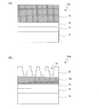
- FIGS. 9 (a) and 9 (b) show SEM images of the surface of the aluminum layer of the mold base 10b of Example 2
- FIGS. 10 (a) and 10 (b) show the aluminum layer of the mold base 30B of Comparative Example 2.
- the SEM image of the surface of is shown.
- FIGS. 9A and 10A are SEM images immediately after the aluminum layer is formed
- FIGS. 9B and 10B are SEM images after immersion in an aqueous phosphoric acid solution. .
- the black dots seen in Fig. 10 (b) are pits (dents). Although it is difficult to understand from FIG. 10A, it is considered that small pits existed in the aluminum layer immediately after film formation.
- the mold base 30B of Comparative Example 2 is considered to have enlarged pits by being immersed in an aqueous phosphoric acid solution. In the mold base material 30B of Comparative Example 2, it is considered that due to the presence of pits in the aluminum layer, the phosphoric acid aqueous solution entered from the pits and the adhesiveness was lowered.
- a mold base was formed by forming a curable resin layer on both surfaces of the polymer film 12, and the adhesion was examined. This was performed in order to investigate the influence of outgas from the back surface by forming a curable resin layer on both surfaces of the polymer film 12. Also in this case, in the above peel test, “ ⁇ ” was given at any stage.
- the mold base 10b of Example 2 is provided with the inorganic base layer 16 and the buffer layer 17, the mold base 10b has better adhesion than the mold base 10 of Example 1 described above.
- Example 3 In Examples 1 and 2, a mold substrate for producing a clear type moth-eye mold was used, whereas in Example 3, a mold substrate having a surface on which a concavo-convex structure exhibiting an antiglare function was formed. Is used.
- the mold base material of Example 3 has the configuration of the mold base material 10c shown in FIG. 5B, the polymer film 12, and the curable resin layer 14c formed on the surface of the polymer film 12, It has the inorganic base layer 16 formed on the curable resin layer 14c, the buffer layer 17 formed on the inorganic base layer 16, and the aluminum layer 18 formed on the surface of the buffer layer 17.
- the mold substrate of Example 3 was produced as follows. A PET film (made by Kimoto, thickness: 188 ⁇ m) is used as the polymer film 12, and a film-like substrate provided with a curable resin layer 14 c having an uneven structure on the surface that exhibits an antiglare function is provided on the polymer film 12. Prepared. Subsequently, a SiO 2 layer having a thickness of 70 nm was formed as the inorganic underlayer 16 on the curable resin layer 14c. Next, an aluminum oxide layer having a thickness of 150 nm was formed as a buffer layer 17 on the surface of the SiO 2 layer 16. Thereafter, an aluminum layer 18 having a thickness of 1 ⁇ m was formed on the surface of the aluminum oxide layer 17 to produce a mold substrate 10c. The aluminum layer 18 was interrupted each time an aluminum layer having a thickness of 200 nm was deposited, and was formed of five aluminum layers each having a thickness of 200 nm.
- the peeling test was performed on the case where the inverted moth-eye structure was formed through the manufacturing process described with reference to FIGS. 1A to 1E in addition to the above-mentioned “initial stage” and “etching”.
- the anodizing conditions and etching conditions were the same as those in Example 1.
- the mold substrate 10c of Example 3 had an evaluation result of “ ⁇ ” and excellent adhesiveness in any experiment.
- a base material on which a concavo-convex structure exhibiting an antiglare function is formed on a PET film and a TAC film a base material used for production of a polarizing plate can be used, and thus there is an advantage that the base material is easily available.
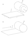
- the flexible mold 100 (FIG. 2B) according to the embodiment of the present invention has a flexible film as the polymer film 12, and can be deformed into a roll shape. By fixing the flexible mold 100 to the outer peripheral surface of the roll-shaped substrate, a roll-shaped moth-eye mold can be obtained. With reference to FIG. 11, a method for producing a roll-shaped moth-eye mold 200 (hereinafter, also referred to as “roll-shaped mold 200”) using the flexible mold 100 will be described.
- a flexible mold 100 and a roll-shaped substrate 40 are prepared.
- the roll-shaped substrate 40 is made of, for example, stainless steel.
- the flexible mold 100 is preferably pasted without forming an air layer between the roll-shaped substrate 40, and is preferably pasted without wrinkles or twists.
- the fixing methods described above there is an advantage that reworking can be easily performed if the method is a method in which an adhesive layer having a weak adhesive force is provided and fixed, or a method in which an electrostatic adsorption structure is provided and fixed on a roll-shaped substrate 40.
- the flexible mold 100 since the flexible mold 100 is wound around the outer peripheral surface of the roll-shaped base material 40, there is a seam on the outer peripheral surface. 100 may be fixed.
- the roll-shaped moth-eye mold 200 shown in FIG. 11C is obtained.
- a roll-shaped moth-eye mold can be manufactured without going through the step of transferring the uneven structure of the porous alumina layer.
- a general-purpose film can be used as the polymer film 12 of the flexible mold 100, and a film forming apparatus that is widely used for forming an aluminum layer is used. Since this is possible, there is an advantage that no dedicated device is required.
- the flexible mold 100 used for the roll-shaped moth-eye mold 200 can be manufactured by performing anodization and etching by batch processing. Furthermore, when the roundness and straightness of rolls are important parameters, a flexible mold is used on a roll-shaped substrate made of stainless steel (for example, JIS standard SUS) rather than using an aluminum pipe. There is an advantage that the accuracy can be increased by making it fixed.
- a film-like substrate having a polymer film 12 and a curable resin layer 14 formed on the surface of the polymer film 12 is prepared.
- the polymer film 12 is, for example, a PET film having a thickness of 188 ⁇ m.
- a protective film and a support plate are affixed to and peeled from a film-like substrate, in the following, for simplicity, the film-like substrate, protective film, support plate, etc. are referred to as a “substrate”. I will explain.
- a front protective film 64 and a back protective film 62 are attached to the front surface of the curable resin layer 14 and the back surface of the polymer film 12, respectively.
- the front protective film 64 By sticking the front protective film 64, the surface of the curable resin layer 14 can be protected until the step of forming the aluminum layer 18 performed later.
- the back protective film 62 By sticking the back protective film 62, the base material can be provided with a waist. If the thickness of the substrate is small, the substrate may be creased during handling. However, by attaching the back protective film 62, the occurrence of such a fold can be prevented. Further, the back protective film 62 can prevent the back surface of the polymer film 12 from becoming dirty.
- the front protective film 64 is peeled off, and the aluminum layer 18 is formed on the curable resin layer 14.
- the aluminum layer 18 can be formed by, for example, the sputtering method described above.
- the support plate 68 is attached to the back side of the back protective film 62.
- the adhesive layer 66 can be attached.
- the support plate 68 for example, a substrate made of acrylic resin and having a thickness of 3 mm can be used. By attaching the support plate 68, the substrate is bent more than necessary in the treatment liquid (the electrolytic solution in the anodizing step and / or the etching solution in the etching step) in the later step of forming the porous alumina layer 20. Can be suppressed. Therefore, the occurrence of anodic oxidation and / or etching unevenness can be suppressed.
- the adhesive layer 66 and the support plate 68 are peeled off, and the treatment liquid adhering to the back surface of the back protective film 62 is wiped off.
- the treatment liquid adhering to the back surface of the back protective film 62 is wiped off.
- the support plate 68 is pasted again through the adhesive layer 66.
- a release agent is applied to the surface of the porous alumina layer 20.
- the release agent can be applied by, for example, a dip method.
- a roll-shaped base material 40 is prepared, and the base material (the flexible mold 100 and the second front protective film 65 is provided on the outer peripheral surface of the roll-shaped base material 40. ).
- the roll-shaped substrate 40 is a cylindrical substrate having the same configuration as the roll-shaped substrate 40 used in the roll-shaped mold manufacturing method described with reference to FIG. In (g), only a part thereof is schematically shown. In this way, a roll-shaped moth-eye mold 200 is obtained.
- the back protective film 62 is peeled off from the base material immediately before being fixed to the roll base material 40.
- the flexible mold can be fixed by the method described above with reference to FIG.
- the workpiece for example, a curable resin or the like is formed on the surface.
- the applied film to be transferred 72 is disposed on the porous alumina layer 20.
- the transfer may be performed while peeling the second front protective film 65.
- a roll-shaped mold 200 and a polarizing plate 70 are prepared.
- a roll-shaped mold 200 is brought into contact with the polarizing plate 70.
- the roll-shaped mold 200 is brought into contact with the transfer target layer.
- the polarizing plate is generally produced by uniaxial stretching. For example, after dyeing iodine on a PVA film, the film is stretched to produce iodine in the stretching direction. The direction in which the film is stretched is the direction of the polarization axis of the polarizing plate.
- a stress is applied to the polarizing plate in a direction intersecting the polarization axis, the arrangement of iodine molecules is disturbed, so that the selection ratio of polarized light is lowered. Therefore, when the moth-eye structure is formed on the polarizing plate 70 using the roll-shaped mold 200, it is preferable that the polarization axis of the polarizing plate 70 and the circumferential direction of the roll-shaped mold 200 are parallel.
- the long side (y) of the polarizing plate 70 is preferably shorter than the peripheral length (2 ⁇ r) of the roll-shaped mold 200.
- the circumference (2 ⁇ r) of the roll-shaped mold when the polarization axis of the polarizing plate and the circumferential direction of the roll-shaped mold are made parallel will be shown.
- the radius is 200 mm so that the circumference of the roll-shaped mold is longer than the long side.
- a roll with a circumference of 628 mm may be used.
- the circumference of the roll-shaped mold is preferably longer than the long side +23 mm (that is, 592 mm).
- a roll having a radius of 200 mm the circumference can be made longer than the long side +23 mm.
- a roll having a radius of 250 mm for example, a roll having a radius of 250 mm (periphery) so that the circumference of the roll-shaped mold is longer than the long side +23 mm (ie, 723 mm).
- a roll having a length of 785 mm may be used. The same applies to the polarizing plates of display devices of other sizes.
- the inverted moth-eye structure can be superimposed on the mold that forms the concavo-convex structure exhibiting the antiglare function, but according to the embodiment of the present invention, another concavo-convex structure was formed.
- the inverted moth-eye structure can be superimposed on the mold.
- an inverted moth-eye structure can be superimposed on a mold in which a periodic uneven structure is formed.
- lenticular lens for example, lenticular lens, brightness enhancement film (for example, BEF manufactured by Sumitomo 3M), light guide plate, microlens array, Fresnel lens, etc.
- BEF brightness enhancement film
- a moth-eye structure may be superimposed.
- a mold 52 having the same concavo-convex structure as a lenticular lens is prepared.
- the lenticular lens has a structure in which a plurality of semi-cylindrical (semi-cylindrical) lenses are arranged in parallel.
- the overall size is 460 mm ⁇ 365 mm
- the pitch (width of the semi-cylindrical lens) is 20 ⁇ m
- the opening angle is 90 ° (the curved surface of the semi-cylindrical lens and the surface perpendicular to the extending direction of the semi-cylindrical lens)
- a curve in which the crosses and corresponds to a quarter of the circumference) is produced.
- a resin layer (for example, an ultraviolet curable resin layer) 14d is formed to produce a film-like substrate 10d ′.
- the polymer film 12 for example, a COP film or a PET film can be used.
- an inorganic underlayer (for example, SiO 2 layer) 16 and a buffer layer (for example, The aluminum oxide layer) 17 and the aluminum layer 18 are formed by the same method as described above to obtain the mold substrate 10d.
- the mold base 10d the mold 100d (FIG. 14) is obtained by repeating the anodic oxidation and etching by the manufacturing process described with reference to FIGS. 1 (a) to 1 (e).
- a lenticular lens having a moth-eye structure on the surface can be manufactured.
- a roll-shaped mold capable of producing a lenticular lens having a moth-eye structure on the surface is obtained.
- the curable resin layer 14d is formed on the polymer film 12, and then the curable resin layer 14d having a concavo-convex structure in which the concavo-convex structure of the mold 52 is inverted is formed.
- the curable resin layer 14 was formed on the surface of the polymer film 12e on which the periodic concavo-convex structure was formed in advance as shown in FIG. 16, although the film-like substrate 10d ′ (FIG. 15B) was used. A film-like substrate 10e ′ produced in this manner may be used.
- a seam exists on the outer peripheral surface of the roll-shaped mold 200.
- the flexible mold 100 is disposed so that a gap is left between one end and the other end.
- the thickness is doubled at the joint portion, and a step is formed before and after the overlapped portion.
- the step portion is not transferred well.
- the resin may accumulate in a step portion and become uncured. Uncured resin may adhere to the film to be transferred when the film to be transferred is rolled up and stacked, for example, and may contaminate the film to be transferred.
- air may enter the step portion to form an air layer. Due to this air layer, the flexible mold 100 may be peeled off from the roll-shaped substrate 40. Further, the step may be transferred onto the film to be transferred.
- the flexible mold 100 is arranged so that a gap is provided between one end and the other end, for example, a resin or the like is applied to the gap to fill the gap (FIG. 17).
- the resin applied to the gap is indicated by 50.
- the flexible mold 100 is disposed so that a gap is provided between one end and the other end.
- a film substrate having a polymer film having a knurling treatment at the end can be suitably used as the film substrate on which the moth-eye structure is formed.
- the knurling process is to provide a convex portion at the end of the film.
- the knurling process is performed for the purpose of preventing the overlapped films from coming into close contact when wound.
- FIG. 18 shows a schematic cross-sectional view of a film base material 70f having a polymer film 72f that has been knurled.
- the film base material 70f includes a polymer film 72f provided with a plurality of semi-cylindrical (semi-cylindrical) convex portions 73 at both ends, and a photocuring formed on the polymer film 72f.
- a functional resin layer 75 is made of, for example, an ultraviolet curable resin, and has a moth-eye structure on the surface.
- the height of the moth-eye structure from the surface of the polymer film 72f is the height of the protrusion 73 from the surface of the polymer film 72f (hereinafter, “ It is also referred to as “the height of the convex portion 73”.) It is preferably formed to be as follows. If the height of the moth-eye structure is higher than the convex portion 73, the moth-eye structure may be damaged by friction with the back surface of the film base material that is overlaid when the film base material is rolled up and stacked. This is because the moth-eye structure may be destroyed.
- the height of the convex portion 73 formed by the knurling process is about several tens of ⁇ m to 100 ⁇ m. Therefore, for example, it is preferable to form the moth-eye structure so that the height from the surface of the polymer film 72f is about 6 ⁇ m to 10 ⁇ m.
- the size of the step is preferably lower than the height of the convex portion 73.
- the photocurable resin layer 75 is preferably formed by applying a resin between the convex portions 73 at both ends of the polymer film 72f. This is because if the resin used for the photocurable resin layer is also applied to the convex portions, the effect of the knurling treatment is suppressed.
- the mold according to the present invention can be widely used for forming a surface having a moth-eye structure, for example, for forming an antireflection film.
Abstract
Priority Applications (6)
| Application Number | Priority Date | Filing Date | Title |
|---|---|---|---|
| RU2011148500/02A RU2481949C1 (ru) | 2009-04-30 | 2010-04-26 | Пресс-форма и способ ее изготовления |
| EP10769495.2A EP2426237B1 (fr) | 2009-04-30 | 2010-04-26 | Moule et procédé de fabrication de celui-ci |
| US13/266,686 US8545708B2 (en) | 2009-04-30 | 2010-04-26 | Mold and manufacturing method therefor |
| JP2010546173A JP4677515B2 (ja) | 2009-04-30 | 2010-04-26 | 型およびその製造方法 |
| BRPI1011897A BRPI1011897A2 (pt) | 2009-04-30 | 2010-04-26 | "molde e método de fabricação do mesmo" |
| CN201080005176.6A CN102292472B (zh) | 2009-04-30 | 2010-04-26 | 模具及其制造方法 |
Applications Claiming Priority (2)
| Application Number | Priority Date | Filing Date | Title |
|---|---|---|---|
| JP2009-111330 | 2009-04-30 | ||
| JP2009111330 | 2009-04-30 |
Publications (1)
| Publication Number | Publication Date |
|---|---|
| WO2010125795A1 true WO2010125795A1 (fr) | 2010-11-04 |
Family
ID=43031953
Family Applications (1)
| Application Number | Title | Priority Date | Filing Date |
|---|---|---|---|
| PCT/JP2010/002989 WO2010125795A1 (fr) | 2009-04-30 | 2010-04-26 | Moule et procédé de fabrication de celui-ci |
Country Status (7)
| Country | Link |
|---|---|
| US (1) | US8545708B2 (fr) |
| EP (1) | EP2426237B1 (fr) |
| JP (1) | JP4677515B2 (fr) |
| CN (1) | CN102292472B (fr) |
| BR (1) | BRPI1011897A2 (fr) |
| RU (1) | RU2481949C1 (fr) |
| WO (1) | WO2010125795A1 (fr) |
Cited By (19)
| Publication number | Priority date | Publication date | Assignee | Title |
|---|---|---|---|---|
| WO2012046808A1 (fr) * | 2010-10-08 | 2012-04-12 | シャープ株式会社 | Procédé de production d'un film anodisé |
| JP2012123102A (ja) * | 2010-12-07 | 2012-06-28 | Toppan Printing Co Ltd | 表示体及びラベル付き物品 |
| JP2012129487A (ja) * | 2010-12-15 | 2012-07-05 | Qinghua Univ | 太陽電池及びその製造方法 |
| JP2012137534A (ja) * | 2010-12-24 | 2012-07-19 | Dainippon Printing Co Ltd | 反射防止フィルム製造用金型 |
| WO2012124498A1 (fr) * | 2011-03-11 | 2012-09-20 | シャープ株式会社 | Matrice, procédé de fabrication pour matrice, et procédé de fabrication pour film imprimé à l'échelle nanométrique |
| US20130094089A1 (en) * | 2010-04-28 | 2013-04-18 | Sharp Kabushiki Kaisha | Mold and process for production of mold |
| JP2013142741A (ja) * | 2012-01-10 | 2013-07-22 | Dainippon Printing Co Ltd | 反射防止フィルム製造用原版 |
| WO2013180009A1 (fr) * | 2012-05-29 | 2013-12-05 | 住友化学株式会社 | Procédé de fabrication de feuille optique, dispositif de traitement de feuille optique et procédé de traitement de feuille optique |
| CN103459680A (zh) * | 2011-04-01 | 2013-12-18 | 夏普株式会社 | 模具的制造方法 |
| JP2014104584A (ja) * | 2012-11-22 | 2014-06-09 | Sumitomo Chemical Co Ltd | 光学シート加工装置 |
| JP2014107017A (ja) * | 2012-11-22 | 2014-06-09 | Sumitomo Chemical Co Ltd | 光学シート加工装置 |
| JP2014116083A (ja) * | 2012-12-06 | 2014-06-26 | Sumitomo Chemical Co Ltd | 光学シート加工装置 |
| US20150083465A1 (en) * | 2012-05-07 | 2015-03-26 | Korea Institute Of Machinery & Materials | Transparent conductive substrate, and method for manufacturing same |
| WO2015159797A1 (fr) * | 2014-04-14 | 2015-10-22 | シャープ株式会社 | Moule, procédé de fabrication d'un moule, film antireflet et procédé de fabrication d'un film antireflet |
| WO2016076239A1 (fr) * | 2014-11-12 | 2016-05-19 | シャープ株式会社 | Procédé de production de moule |
| WO2016080314A1 (fr) * | 2014-11-21 | 2016-05-26 | シャープ株式会社 | Moule et son procédé de fabrication, film antireflet et son procédé de fabrication |
| JP2017032756A (ja) * | 2015-07-31 | 2017-02-09 | 三菱レイヨン株式会社 | 透明フィルム及びその製造方法 |
| WO2017150335A1 (fr) * | 2016-03-02 | 2017-09-08 | シャープ株式会社 | Procédé de fabrication de moule de lentille et moule de lentille |
| US20210197504A1 (en) * | 2018-05-25 | 2021-07-01 | Dexerials Corporation | Resin laminated optical body, light source unit, optical unit, light irradiation device, image display device, method for manufacturing resin laminated optical body, and method for manufacturing light source unit |
Families Citing this family (24)
| Publication number | Priority date | Publication date | Assignee | Title |
|---|---|---|---|---|
| BR112012004984A2 (pt) * | 2009-09-04 | 2016-05-03 | Sharp Kk | método para formação de camada anodizada, método para produção de molde, método para produção de película antirefletiva, e molde e película antirefletiva |
| WO2011043464A1 (fr) | 2009-10-09 | 2011-04-14 | シャープ株式会社 | Moule, procédé de production associé, et film antireflet |
| US9193096B2 (en) * | 2010-02-24 | 2015-11-24 | Sharp Kabushiki Kaisha | Die, die production method, and production of antireflection film |
| WO2011162125A1 (fr) * | 2010-06-21 | 2011-12-29 | シャープ株式会社 | Panneau d'affichage équipé d'une plaque avant, dispositif d'affichage, et composition à base de résine |
| TW201325884A (zh) * | 2011-12-29 | 2013-07-01 | Hon Hai Prec Ind Co Ltd | 光學薄膜壓印滾輪及該滾輪之製作方法 |
| EP2626450A1 (fr) * | 2012-02-08 | 2013-08-14 | Nederlandse Organisatie voor toegepast- natuurwetenschappelijk onderzoek TNO | Procédé de fabrication de nanostructures sur une surface, sur un moule et sur un élément optique, et élément optique ainsi fabriqué |
| CN103297565B (zh) | 2012-02-24 | 2015-07-22 | 比亚迪股份有限公司 | 一种手机壳体及其制备方法 |
| CN103286996B (zh) | 2012-02-24 | 2015-03-25 | 比亚迪股份有限公司 | 一种铝合金树脂复合体的制备方法及其制备的铝合金树脂复合体 |
| CN103286908B (zh) | 2012-02-24 | 2015-09-30 | 比亚迪股份有限公司 | 一种金属树脂一体化成型方法和一种金属树脂复合体 |
| CN103287009B (zh) | 2012-02-24 | 2015-03-25 | 比亚迪股份有限公司 | 一种铝合金树脂复合体的制备方法及其制备的铝合金树脂复合体 |
| CN103286910B (zh) | 2012-02-24 | 2015-09-30 | 比亚迪股份有限公司 | 一种金属树脂一体化成型方法和一种金属树脂复合体 |
| CN103286909B (zh) | 2012-02-24 | 2015-09-30 | 比亚迪股份有限公司 | 一种金属树脂一体化成型方法和一种金属树脂复合体 |
| CN103286995B (zh) | 2012-02-24 | 2015-06-24 | 比亚迪股份有限公司 | 一种铝合金树脂复合体的制备方法及其制备的铝合金树脂复合体 |
| EP2855740A4 (fr) | 2012-05-28 | 2016-03-09 | Byd Co Ltd | Composite de métal et son procédé de préparation, composite métal-résine et son procédé de préparation |
| TWI465301B (zh) * | 2012-09-25 | 2014-12-21 | Univ Southern Taiwan Sci & Tec | 多孔性氧化鋁模板之製作裝置 |
| KR20150067299A (ko) * | 2012-12-13 | 2015-06-17 | 오지 홀딩스 가부시키가이샤 | 광학 소자 제작용 금형 및 그 제조 방법, 광학 소자 |
| EP3520985B1 (fr) * | 2013-03-14 | 2022-07-20 | Stratasys Ltd. | Moules à base de polymère et procédés de fabrication associés |
| WO2015022935A1 (fr) * | 2013-08-14 | 2015-02-19 | 三菱レイヨン株式会社 | Procédés de fabrication de moule pour nano-impression cylindrique, et de moule de reproduction pour nano-impression |
| CN104746066B (zh) | 2013-12-31 | 2017-07-04 | 比亚迪股份有限公司 | 一种金属与塑料的结合材料及其制备方法及制备的结合材料 |
| US10695955B2 (en) * | 2014-11-06 | 2020-06-30 | Sharp Kabushiki Kaisha | Mold manufacturing method and anti-reflective film manufacturing method |
| CN106929897A (zh) * | 2015-12-30 | 2017-07-07 | 比亚迪股份有限公司 | 一种铝合金壳体及其制备方法 |
| US20170199309A1 (en) * | 2016-01-12 | 2017-07-13 | Optivision Technology Inc. | Optical device and diffusion film |
| JP6042002B1 (ja) * | 2016-01-26 | 2016-12-14 | 綜研化学株式会社 | 構造体 |
| KR102234424B1 (ko) * | 2019-08-07 | 2021-04-01 | 한국과학기술원 | 세탁 가능한 나노 층화 봉지 구조체 및 이를 포함하는 전자 장치 |
Citations (6)
| Publication number | Priority date | Publication date | Assignee | Title |
|---|---|---|---|---|
| JPS53103754A (en) * | 1977-02-18 | 1978-09-09 | Minnesota Mining & Mfg | Fine particle coating to improve reflection and percolation |
| JP2000334745A (ja) | 1999-06-01 | 2000-12-05 | Toppan Printing Co Ltd | ロール状の樹脂型とその樹脂型を用いたレンズシートの製造方法 |
| JP2001517319A (ja) | 1997-03-04 | 2001-10-02 | フラウンホファー.ゲゼルシャフト.ツール.フォルデンウング.デール.アンゲヴァンドテン.フォルシュング.エー.ファウ. | 反射防止膜とその製法 |
| JP2003531962A (ja) | 2000-04-28 | 2003-10-28 | アルコーブ サーフィシーズ ゲーエムベーハー | 型押し具、これを製造する方法、加工物の表面を構築する方法、及び陽極酸化表面層の使用 |
| JP2005156695A (ja) | 2003-11-21 | 2005-06-16 | Kanagawa Acad Of Sci & Technol | 反射防止膜及びその製造方法、並びに反射防止膜作製用スタンパ及びその製造方法 |
| WO2006059686A1 (fr) | 2004-12-03 | 2006-06-08 | Sharp Kabushiki Kaisha | Materiau empechant la reflexion, element optique, dispositif d’affichage, procede de fabrication d’une matrice et procede de fabrication d’un materiau empechant la reflexion a l’aide de la matrice |
Family Cites Families (12)
| Publication number | Priority date | Publication date | Assignee | Title |
|---|---|---|---|---|
| JPS5539663B2 (fr) * | 1972-05-23 | 1980-10-13 | ||
| US4193848A (en) | 1973-08-13 | 1980-03-18 | Swiss Aluminium Ltd. | Process for the production of composite material |
| US4252843A (en) * | 1977-02-18 | 1981-02-24 | Minnesota Mining And Manufacturing Company | Process for forming a microstructured transmission and reflectance modifying coating |
| US5759455A (en) * | 1994-07-08 | 1998-06-02 | Canon Kabushiki Kaisha | Roller-shaped stamper for fabricating optical scales |
| JP3436983B2 (ja) | 1994-09-02 | 2003-08-18 | 富士通株式会社 | モールド成形品の分離方法 |
| JP2955704B2 (ja) | 1995-07-25 | 1999-10-04 | 株式会社有沢製作所 | 航空機用の液晶プロジェクター用反射型スクリーン及び液晶プロジェクター用反射型スクリーンの製造方法 |
| JP3440754B2 (ja) | 1997-05-19 | 2003-08-25 | 信越化学工業株式会社 | 室温硬化性オルガノポリシロキサン組成物 |
| RU2133049C1 (ru) * | 1997-12-16 | 1999-07-10 | Открытое акционерное общество "Компат" | Способ нанесения просветляющего многослойного покрытия на поверхность оптического элемента и установка для осуществления способа |
| US7066234B2 (en) | 2001-04-25 | 2006-06-27 | Alcove Surfaces Gmbh | Stamping tool, casting mold and methods for structuring a surface of a work piece |
| DE502005009665D1 (de) * | 2004-06-22 | 2010-07-15 | Boegli Gravures Sa | Vorrichtung und Verfahren zum Satinieren und Prägen von Flachmaterial |
| CN101484614B (zh) * | 2006-06-30 | 2011-09-07 | 三菱丽阳株式会社 | 铸模、铸模的制造方法以及片材的制造方法 |
| JP4648995B2 (ja) | 2009-04-09 | 2011-03-09 | シャープ株式会社 | 型およびその製造方法 |
-
2010
- 2010-04-26 JP JP2010546173A patent/JP4677515B2/ja active Active
- 2010-04-26 WO PCT/JP2010/002989 patent/WO2010125795A1/fr active Application Filing
- 2010-04-26 US US13/266,686 patent/US8545708B2/en active Active
- 2010-04-26 CN CN201080005176.6A patent/CN102292472B/zh active Active
- 2010-04-26 RU RU2011148500/02A patent/RU2481949C1/ru active
- 2010-04-26 BR BRPI1011897A patent/BRPI1011897A2/pt not_active IP Right Cessation
- 2010-04-26 EP EP10769495.2A patent/EP2426237B1/fr not_active Not-in-force
Patent Citations (6)
| Publication number | Priority date | Publication date | Assignee | Title |
|---|---|---|---|---|
| JPS53103754A (en) * | 1977-02-18 | 1978-09-09 | Minnesota Mining & Mfg | Fine particle coating to improve reflection and percolation |
| JP2001517319A (ja) | 1997-03-04 | 2001-10-02 | フラウンホファー.ゲゼルシャフト.ツール.フォルデンウング.デール.アンゲヴァンドテン.フォルシュング.エー.ファウ. | 反射防止膜とその製法 |
| JP2000334745A (ja) | 1999-06-01 | 2000-12-05 | Toppan Printing Co Ltd | ロール状の樹脂型とその樹脂型を用いたレンズシートの製造方法 |
| JP2003531962A (ja) | 2000-04-28 | 2003-10-28 | アルコーブ サーフィシーズ ゲーエムベーハー | 型押し具、これを製造する方法、加工物の表面を構築する方法、及び陽極酸化表面層の使用 |
| JP2005156695A (ja) | 2003-11-21 | 2005-06-16 | Kanagawa Acad Of Sci & Technol | 反射防止膜及びその製造方法、並びに反射防止膜作製用スタンパ及びその製造方法 |
| WO2006059686A1 (fr) | 2004-12-03 | 2006-06-08 | Sharp Kabushiki Kaisha | Materiau empechant la reflexion, element optique, dispositif d’affichage, procede de fabrication d’une matrice et procede de fabrication d’un materiau empechant la reflexion a l’aide de la matrice |
Cited By (35)
| Publication number | Priority date | Publication date | Assignee | Title |
|---|---|---|---|---|
| US20130094089A1 (en) * | 2010-04-28 | 2013-04-18 | Sharp Kabushiki Kaisha | Mold and process for production of mold |
| US9405043B2 (en) * | 2010-04-28 | 2016-08-02 | Sharp Kabushiki Kaisha | Mold and process for production of mold |
| WO2012046808A1 (fr) * | 2010-10-08 | 2012-04-12 | シャープ株式会社 | Procédé de production d'un film anodisé |
| JP5595511B2 (ja) * | 2010-10-08 | 2014-09-24 | シャープ株式会社 | 陽極酸化膜の製造方法 |
| US9133558B2 (en) | 2010-10-08 | 2015-09-15 | Sharp Kabushiki Kaisha | Method for producing anodized film |
| JP2012123102A (ja) * | 2010-12-07 | 2012-06-28 | Toppan Printing Co Ltd | 表示体及びラベル付き物品 |
| JP2012129487A (ja) * | 2010-12-15 | 2012-07-05 | Qinghua Univ | 太陽電池及びその製造方法 |
| JP2012137534A (ja) * | 2010-12-24 | 2012-07-19 | Dainippon Printing Co Ltd | 反射防止フィルム製造用金型 |
| WO2012124498A1 (fr) * | 2011-03-11 | 2012-09-20 | シャープ株式会社 | Matrice, procédé de fabrication pour matrice, et procédé de fabrication pour film imprimé à l'échelle nanométrique |
| CN103415381A (zh) * | 2011-03-11 | 2013-11-27 | 夏普株式会社 | 模具、模具的制造方法、以及纳米压印膜的制造方法 |
| US10155340B2 (en) | 2011-03-11 | 2018-12-18 | Sharp Kabushiki Kaisha | Mold, method for producing mold, and method for producing nanoimprint film |
| JP5576555B2 (ja) * | 2011-03-11 | 2014-08-20 | シャープ株式会社 | ナノインプリントフィルムの製造方法 |
| CN103459680A (zh) * | 2011-04-01 | 2013-12-18 | 夏普株式会社 | 模具的制造方法 |
| US20140197036A1 (en) * | 2011-04-01 | 2014-07-17 | Geomatec Co., Ltd. | Mold production method |
| US9512535B2 (en) | 2011-04-01 | 2016-12-06 | Sharp Kabushiki Kaisha | Mold production method |
| JP2013142741A (ja) * | 2012-01-10 | 2013-07-22 | Dainippon Printing Co Ltd | 反射防止フィルム製造用原版 |
| US20150083465A1 (en) * | 2012-05-07 | 2015-03-26 | Korea Institute Of Machinery & Materials | Transparent conductive substrate, and method for manufacturing same |
| WO2013180009A1 (fr) * | 2012-05-29 | 2013-12-05 | 住友化学株式会社 | Procédé de fabrication de feuille optique, dispositif de traitement de feuille optique et procédé de traitement de feuille optique |
| JP2014104584A (ja) * | 2012-11-22 | 2014-06-09 | Sumitomo Chemical Co Ltd | 光学シート加工装置 |
| JP2014107017A (ja) * | 2012-11-22 | 2014-06-09 | Sumitomo Chemical Co Ltd | 光学シート加工装置 |
| JP2014116083A (ja) * | 2012-12-06 | 2014-06-26 | Sumitomo Chemical Co Ltd | 光学シート加工装置 |
| US10549458B2 (en) | 2014-04-14 | 2020-02-04 | Sharp Kabushiki Kaisha | Mold, method for producing mold, anti-reflection film and method for producing anti-reflection film |
| JPWO2015159797A1 (ja) * | 2014-04-14 | 2017-04-13 | シャープ株式会社 | 型、型の製造方法、反射防止膜および反射防止膜の製造方法 |
| WO2015159797A1 (fr) * | 2014-04-14 | 2015-10-22 | シャープ株式会社 | Moule, procédé de fabrication d'un moule, film antireflet et procédé de fabrication d'un film antireflet |
| WO2016076239A1 (fr) * | 2014-11-12 | 2016-05-19 | シャープ株式会社 | Procédé de production de moule |
| JPWO2016076239A1 (ja) * | 2014-11-12 | 2017-08-17 | シャープ株式会社 | 型の製造方法 |
| WO2016080314A1 (fr) * | 2014-11-21 | 2016-05-26 | シャープ株式会社 | Moule et son procédé de fabrication, film antireflet et son procédé de fabrication |
| JPWO2016080314A1 (ja) * | 2014-11-21 | 2017-11-09 | シャープ株式会社 | 型、型の製造方法、反射防止膜および反射防止膜の製造方法 |
| JP2017032756A (ja) * | 2015-07-31 | 2017-02-09 | 三菱レイヨン株式会社 | 透明フィルム及びその製造方法 |
| CN108699721A (zh) * | 2016-03-02 | 2018-10-23 | 夏普株式会社 | 透镜用模具的制造方法及透镜用模具 |
| WO2017150335A1 (fr) * | 2016-03-02 | 2017-09-08 | シャープ株式会社 | Procédé de fabrication de moule de lentille et moule de lentille |
| JPWO2017150335A1 (ja) * | 2016-03-02 | 2018-12-13 | シャープ株式会社 | レンズ用型の製造方法およびレンズ用型 |
| CN108699721B (zh) * | 2016-03-02 | 2021-02-19 | 夏普株式会社 | 透镜用模具的制造方法及透镜用模具 |
| US20210197504A1 (en) * | 2018-05-25 | 2021-07-01 | Dexerials Corporation | Resin laminated optical body, light source unit, optical unit, light irradiation device, image display device, method for manufacturing resin laminated optical body, and method for manufacturing light source unit |
| EP3805818A4 (fr) * | 2018-05-25 | 2022-01-19 | Dexerials Corporation | Corps optique recouvert d'une couche de résine, unité source de lumière, unité optique, dispositif d'exposition à la lumière, dispositif d'affichage d'image, procédé de fabrication d'un corps optique recouvert d'une couche de résine et procédé de fabrication d'une unité source de lumière |
Also Published As
| Publication number | Publication date |
|---|---|
| CN102292472B (zh) | 2014-04-02 |
| JP4677515B2 (ja) | 2011-04-27 |
| EP2426237A4 (fr) | 2013-01-09 |
| RU2481949C1 (ru) | 2013-05-20 |
| US20120043297A1 (en) | 2012-02-23 |
| US8545708B2 (en) | 2013-10-01 |
| EP2426237A1 (fr) | 2012-03-07 |
| BRPI1011897A2 (pt) | 2016-04-12 |
| EP2426237B1 (fr) | 2017-11-08 |
| CN102292472A (zh) | 2011-12-21 |
| JPWO2010125795A1 (ja) | 2012-10-25 |
Similar Documents
| Publication | Publication Date | Title |
|---|---|---|
| JP4677515B2 (ja) | 型およびその製造方法 | |
| JP4648995B2 (ja) | 型およびその製造方法 | |
| JP5027346B2 (ja) | 型および型の製造方法ならびに反射防止膜の製造方法 | |
| JP4916597B2 (ja) | 型および型の製造方法ならびに反射防止膜 | |
| JP4583506B2 (ja) | 反射防止膜、および反射防止膜を備える光学素子、ならびに、スタンパ、およびスタンパの製造方法、ならびに反射防止膜の製造方法 | |
| JP5615971B2 (ja) | 型の製造方法 | |
| JP4796216B2 (ja) | 型および型の製造方法ならびに反射防止膜 | |
| WO2011043464A1 (fr) | Moule, procédé de production associé, et film antireflet | |
| JP2010168664A (ja) | 型の製造方法および型を用いた反射防止膜の製造方法 | |
| JP6458051B2 (ja) | 型および型の製造方法ならびに反射防止膜 | |
| JP5027347B2 (ja) | 型および型の製造方法 | |
| JP5833763B2 (ja) | 型の製造方法 |
Legal Events
| Date | Code | Title | Description |
|---|---|---|---|
| WWE | Wipo information: entry into national phase |
Ref document number: 201080005176.6 Country of ref document: CN |
|
| WWE | Wipo information: entry into national phase |
Ref document number: 2010546173 Country of ref document: JP |
|
| 121 | Ep: the epo has been informed by wipo that ep was designated in this application |
Ref document number: 10769495 Country of ref document: EP Kind code of ref document: A1 |
|
| WWE | Wipo information: entry into national phase |
Ref document number: 13266686 Country of ref document: US |
|
| NENP | Non-entry into the national phase |
Ref country code: DE |
|
| WWE | Wipo information: entry into national phase |
Ref document number: 2476/MUMNP/2011 Country of ref document: IN |
|
| REEP | Request for entry into the european phase |
Ref document number: 2010769495 Country of ref document: EP |
|
| WWE | Wipo information: entry into national phase |
Ref document number: 2010769495 Country of ref document: EP |
|
| ENP | Entry into the national phase |
Ref document number: 2011148500 Country of ref document: RU Kind code of ref document: A |
|
| REG | Reference to national code |
Ref country code: BR Ref legal event code: B01A Ref document number: PI1011897 Country of ref document: BR |
|
| ENP | Entry into the national phase |
Ref document number: PI1011897 Country of ref document: BR Kind code of ref document: A2 Effective date: 20111028 |