WO2010125679A1 - 太陽電池セル - Google Patents
太陽電池セル Download PDFInfo
- Publication number
- WO2010125679A1 WO2010125679A1 PCT/JP2009/058493 JP2009058493W WO2010125679A1 WO 2010125679 A1 WO2010125679 A1 WO 2010125679A1 JP 2009058493 W JP2009058493 W JP 2009058493W WO 2010125679 A1 WO2010125679 A1 WO 2010125679A1
- Authority
- WO
- WIPO (PCT)
- Prior art keywords
- electrode
- receiving surface
- surface lead
- back surface
- lead bonding
- Prior art date
Links
- 239000000758 substrate Substances 0.000 claims abstract description 57
- WABPQHHGFIMREM-UHFFFAOYSA-N lead(0) Chemical compound [Pb] WABPQHHGFIMREM-UHFFFAOYSA-N 0.000 claims description 41
- 239000004065 semiconductor Substances 0.000 claims description 23
- BQCADISMDOOEFD-UHFFFAOYSA-N Silver Chemical compound [Ag] BQCADISMDOOEFD-UHFFFAOYSA-N 0.000 abstract description 35
- 229910052709 silver Inorganic materials 0.000 abstract description 35
- 239000004332 silver Substances 0.000 abstract description 35
- XUIMIQQOPSSXEZ-UHFFFAOYSA-N Silicon Chemical compound [Si] XUIMIQQOPSSXEZ-UHFFFAOYSA-N 0.000 abstract description 22
- 229910052710 silicon Inorganic materials 0.000 abstract description 22
- 239000010703 silicon Substances 0.000 abstract description 22
- 210000004027 cell Anatomy 0.000 description 47
- RYGMFSIKBFXOCR-UHFFFAOYSA-N Copper Chemical compound [Cu] RYGMFSIKBFXOCR-UHFFFAOYSA-N 0.000 description 5
- 238000005336 cracking Methods 0.000 description 5
- 230000000694 effects Effects 0.000 description 5
- 239000004575 stone Substances 0.000 description 3
- XAGFODPZIPBFFR-UHFFFAOYSA-N aluminium Chemical compound [Al] XAGFODPZIPBFFR-UHFFFAOYSA-N 0.000 description 2
- 229910052782 aluminium Inorganic materials 0.000 description 2
- 239000012141 concentrate Substances 0.000 description 1
- 229910052802 copper Inorganic materials 0.000 description 1
- 239000010949 copper Substances 0.000 description 1
- 239000000284 extract Substances 0.000 description 1
- 239000000463 material Substances 0.000 description 1
- 230000000116 mitigating effect Effects 0.000 description 1
Images


Classifications
-
- H—ELECTRICITY
- H01—ELECTRIC ELEMENTS
- H01L—SEMICONDUCTOR DEVICES NOT COVERED BY CLASS H10
- H01L31/00—Semiconductor devices sensitive to infrared radiation, light, electromagnetic radiation of shorter wavelength or corpuscular radiation and specially adapted either for the conversion of the energy of such radiation into electrical energy or for the control of electrical energy by such radiation; Processes or apparatus specially adapted for the manufacture or treatment thereof or of parts thereof; Details thereof
- H01L31/04—Semiconductor devices sensitive to infrared radiation, light, electromagnetic radiation of shorter wavelength or corpuscular radiation and specially adapted either for the conversion of the energy of such radiation into electrical energy or for the control of electrical energy by such radiation; Processes or apparatus specially adapted for the manufacture or treatment thereof or of parts thereof; Details thereof adapted as photovoltaic [PV] conversion devices
- H01L31/042—PV modules or arrays of single PV cells
- H01L31/05—Electrical interconnection means between PV cells inside the PV module, e.g. series connection of PV cells
- H01L31/0504—Electrical interconnection means between PV cells inside the PV module, e.g. series connection of PV cells specially adapted for series or parallel connection of solar cells in a module
-
- H—ELECTRICITY
- H01—ELECTRIC ELEMENTS
- H01L—SEMICONDUCTOR DEVICES NOT COVERED BY CLASS H10
- H01L31/00—Semiconductor devices sensitive to infrared radiation, light, electromagnetic radiation of shorter wavelength or corpuscular radiation and specially adapted either for the conversion of the energy of such radiation into electrical energy or for the control of electrical energy by such radiation; Processes or apparatus specially adapted for the manufacture or treatment thereof or of parts thereof; Details thereof
- H01L31/02—Details
- H01L31/0224—Electrodes
- H01L31/022408—Electrodes for devices characterised by at least one potential jump barrier or surface barrier
- H01L31/022425—Electrodes for devices characterised by at least one potential jump barrier or surface barrier for solar cells
- H01L31/022433—Particular geometry of the grid contacts
-
- Y—GENERAL TAGGING OF NEW TECHNOLOGICAL DEVELOPMENTS; GENERAL TAGGING OF CROSS-SECTIONAL TECHNOLOGIES SPANNING OVER SEVERAL SECTIONS OF THE IPC; TECHNICAL SUBJECTS COVERED BY FORMER USPC CROSS-REFERENCE ART COLLECTIONS [XRACs] AND DIGESTS
- Y02—TECHNOLOGIES OR APPLICATIONS FOR MITIGATION OR ADAPTATION AGAINST CLIMATE CHANGE
- Y02E—REDUCTION OF GREENHOUSE GAS [GHG] EMISSIONS, RELATED TO ENERGY GENERATION, TRANSMISSION OR DISTRIBUTION
- Y02E10/00—Energy generation through renewable energy sources
- Y02E10/50—Photovoltaic [PV] energy
Definitions
- the present invention relates to a solar battery cell that includes a lead wire that is joined to an electrode and extracts an electrical output, and can reduce cell cracking after joining the lead wire.
- a lead wire made of a flat copper wire is joined to the solar battery cell for the purpose of extracting electric output.
- This lead wire contracts when it is cooled to room temperature from a high temperature state immediately after bonding.
- the shrinkage of the lead wire causes warpage or local deformation of the substrate, causing cracking of the solar battery cell.
- a lead junction electrode extending in a straight line is formed on the light receiving surface (front surface) of the substrate of the solar battery cell for the purpose of joining the lead wires.
- lead bonding electrodes are formed in a dot shape (stepping stones) with a predetermined interval for the purpose of bonding lead wires. Then, the portion other than the dot-shaped lead bonding electrode on the back surface of the substrate is entirely an aluminum electrode.
- Patent Document 1 has a certain effect in order to alleviate the warpage of the solar battery cell, but the cell crack caused by local deformation due to stress concentration as described below. Did not have a sufficient effect.
- the lead wire when a lead wire made of a flat copper wire is bonded to a silver lead bonding electrode, the lead wire (copper) has a larger shrinkage rate than the lead bonding electrode (silver), so the lead wire is formed on the surface of the solar cell. Stress is applied so as to shrink the formed lead bonding electrode. The stress acting so that the lead wire contracts the lead bonding electrode is similarly generated in the back surface lead bonding electrode by the back surface lead wire.
- the stress applied to the substrate from the lead bonding electrode on the light receiving surface side and the stress applied to the substrate from the lead bonding electrode on the back surface side are applied to the same position across the substrate, the stress concentrates and causes cell cracking.
- Patent Document 1 has a portion where the lead bonding electrode on the light receiving surface side and the lead bonding electrode on the back surface side overlap with each other across the substrate, and stress concentration occurs in this portion. . Therefore, an effective improvement measure against this stress concentration has been desired.
- the present invention has been made in view of the above, and effectively reduces the concentration of stress applied to the substrate from the lead junction electrode of the solar battery cell, thereby preventing the occurrence of cell cracking by preventing local excessive deformation. It aims at obtaining the photovoltaic cell which can reduce.
- a solar battery cell includes a plurality of grid electrodes formed in parallel on a light receiving surface of a semiconductor substrate, and substantially the grid electrodes.
- a solar cell that has a light receiving surface lead bonding electrode that extends on a first orthogonal straight line and is bonded to the light receiving surface lead wire, and has a back surface lead bonding electrode that is bonded to the back surface lead wire on the back surface of the semiconductor substrate.
- the back surface lead bonding electrode is formed in a dot shape at a predetermined interval on a second straight line substantially opposed to the first straight line across the semiconductor substrate, and the light receiving surface lead bonding electrode is formed on the semiconductor substrate. It is characterized by being intermittently formed on the first straight line so that a portion facing the back surface lead bonding electrode is missing.
- a solar battery cell according to a second aspect of the present invention is formed on a light receiving surface of a semiconductor substrate, extending in parallel on a plurality of grid electrodes formed on a first straight line substantially orthogonal to the grid electrodes.
- the back surface lead bonding electrode bonded to the light receiving surface lead wire and having the back surface lead bonding electrode bonded to the back surface lead wire on the back surface of the semiconductor substrate.
- the width of the portion of the light receiving surface lead bonding electrode facing the back surface lead bonding electrode is formed in a dot shape on the second straight line substantially opposed across the straight line and the semiconductor substrate. It is characterized in that it is larger than the width of the part that does not oppose to.
- the back surface lead bonding electrode is formed in a dot shape with a predetermined interval on the second straight line that is substantially opposed to the first straight line across the semiconductor substrate. Since the light receiving surface lead bonding electrode is intermittently formed on the first straight line so that the portion facing the back surface lead bonding electrode is missing across the semiconductor substrate, the light receiving surface lead bonding electrode and the back surface The stress concentration that occurs when the lead bonding electrode overlaps can be alleviated, and the stress generated at the edge when the light receiving surface lead wire protrudes from the light receiving surface lead bonding electrode and the back surface lead bonding When the electrode protrudes from the back surface lead wire, the stress generated at the edge of the electrode does not overlap, and the stress concentration is reduced against the stress generated when the lead wire protrudes from the lead bonding electrode. Since it is an effect that it is possible to reduce the occurrence of cell cracking in relieving the localized excessive deformation.
- the back surface lead junction electrode is formed in a dot shape with a predetermined interval on the second straight line substantially opposed to the first straight line across the semiconductor substrate.
- the width of the portion of the light receiving surface lead bonding electrode facing the back surface lead bonding electrode is larger than the width of the portion not facing the back surface lead bonding electrode and larger than the width of the light receiving surface lead wire.
- the stress generated at the edge does not overlap, and when the lead wire protrudes from the lead bonding electrode Since stress concentration can be relaxed with respect to the generated stress, it is possible to reduce the occurrence of cell cracks by mitigating local excessive deformation.
- the width of only the portion of the light receiving surface lead bonding electrode facing the back surface lead bonding electrode is made larger than the width of the portion not facing the back surface lead bonding electrode, so that the width of the entire light receiving surface lead bonding electrode is increased. Since it does not increase, there is an effect that an improvement in cost can be suppressed.
- FIG. 1 is a plan view of the light receiving surface side of the solar battery cell according to Embodiment 1 of the present invention.
- FIG. 2 is a rear view of FIG. 3 is a cross-sectional view taken along the line AA in FIG.
- FIG. 4 is a plan view showing a state in which the light receiving surface lead wire is bonded to the light receiving surface lead bonding electrode.
- FIG. 5 is a back view showing a state in which the back surface lead wire is bonded to the back surface lead bonding electrode.
- FIG. 6 is a perspective view showing a state in which the light receiving surfaces and the back surfaces of a plurality of solar cells are connected by lead wires.
- FIG. 7 is an enlarged view showing a portion B of FIG.
- FIG. 8 is an enlarged view corresponding to FIG.
- FIG. 9 is a plan view of the light receiving surface side of the solar battery cell according to Embodiment 2 of the present invention.
- FIG. 10 is a rear view of FIG.
- FIG. 11 is an enlarged view showing a portion C of FIG.
- a semiconductor substrate is described as a silicon substrate, a light receiving surface lead bonding electrode as a bus bar electrode, a lead wire as a tab wire, and a back surface lead bonding electrode as a silver electrode.
- the present invention is not limited to the embodiments.
- FIG. 1 is a plan view of the light receiving surface side of the solar battery cell according to Embodiment 1 of the present invention.
- FIG. 2 is a rear view of FIG. 3 is a cross-sectional view taken along the line AA in FIG.
- FIG. 4 is a plan view showing a state in which the light receiving surface lead wire is bonded to the light receiving surface lead bonding electrode.
- FIG. 5 is a back view showing a state in which the back surface lead wire is bonded to the back surface lead bonding electrode.
- FIG. 6 is a perspective view showing a state in which a plurality of solar cells are connected by light receiving surface lead wires and back surface lead wires.
- FIG. 7 is an enlarged view showing a portion B of FIG.
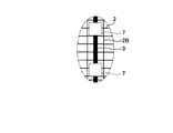
- a plurality of thin grid electrodes 2 that collect current from the entire cell surface while securing a light receiving area as much as possible are provided on the semiconductor substrate 1.
- two bus bar electrodes (light-receiving surface lead bonding electrodes) 3 are provided on a straight line (first straight line) over almost the entire length of the semiconductor substrate 1 substantially perpendicular to the grid electrode 2.
- a light-receiving surface tab wire (light-receiving surface lead wire) 5 is joined over substantially the entire length of the upper surface of the bus bar electrode 3 (in FIG.
- the light-receiving surface tab wire 5 is shown by a one-dot chain line).
- the width of the light receiving surface side tab line 5 is the same as or slightly smaller than the bus bar electrode 3.
- the light-receiving surface tab line 5 has an extension 5a that protrudes outward from the cell surface in order to connect the silicon substrates 1 in series.
- the light-receiving surface tab wire 5 is a flat copper wire generally used as a solar cell lead wire.
- a plurality of dot-like silver electrodes (back side lead bonding electrodes) 7 are provided in two rows with a predetermined interval.
- the silver electrodes 7 arranged in two rows are provided in a stepping stone shape at regular intervals on a straight line (second straight line) facing the bus bar electrode 3.
- a back surface tab wire (back surface lead wire) 8 is joined to the upper surface of the silver electrode 7 over almost the entire length of the row (in FIG. 2, the back surface tab wire 8 overlaps).
- the area is indicated by a dashed line).
- the width of the back surface tab line 8 is smaller than the width of the silver electrode 7.
- the back surface tab wire 8 is also a rectangular copper wire generally used as a solar cell lead wire.
- the light-receiving surface tab line 5 and the back surface tab line 8 are separate members, but may be a single continuous tab line (lead wire).
- the plurality of silicon substrates 1 provided side by side extend the light receiving surface tab line 5 extending from the light receiving surface side to the back surface side of the adjacent silicon substrate 1, and the back surface tab of the adjacent silicon substrate 1.
- the wires 8 are sequentially electrically connected in series.
- FIG. 6 it is set as the perspective view which raised the back surface of the semiconductor substrate 1 so that the connection location of the light-receiving surface tab line 5 and the back surface tab line 8 can be seen.
- the bus-bar electrode 3 is intermittent so that the part of the position which has the silver electrode 7 in the back surface side of the silicon substrate 1 may be missing. Is formed. That is, in the solar battery cell 101 of the present embodiment, the bus bar electrode 3 and the silver electrode 7 do not exist at positions facing each other across the silicon substrate 1. In addition, in FIG. 1 thru
- a detour portion 3a is provided between the adjacent bus bar electrodes 3.
- the detour circuit portion 3 a is formed of the same thin line as the grid electrode 2, is formed by detouring the missing portion, and connects the grid electrode 2 with the end portion facing the missing portion of the bus bar electrode 3.
- the second grid electrode 2 ⁇ / b> B is formed orthogonal to the grid electrode 2 and connects the plurality of grid electrodes 2.
- the solar battery cell 101 is formed by extending the plurality of grid electrodes 2 formed in parallel to the light receiving surface of the silicon substrate 1 and the first straight line orthogonal to the grid electrodes 2.
- the solar cell has a light receiving surface tab wire 5 and a bus bar electrode 3 to be joined, and a silver electrode 7 to be joined to the back surface tab wire 8 on the back surface of the silicon substrate 1.
- the silver electrode 7 is formed in the form of dots at a predetermined interval on the second straight line facing the first straight line and the silicon substrate 1, and the bus bar electrode 3 is formed of silver on the silicon substrate 1. It is intermittently formed on the first straight line so that a portion facing the electrode 7 is missing.
- FIG. FIG. 9 is a plan view of the light receiving surface side of the solar battery cell according to Embodiment 2 of the present invention.
- FIG. 10 is a rear view of FIG.
- FIG. 11 is an enlarged view showing a portion C of FIG.
- four bus bar electrodes (light-receiving surface lead bonding electrodes) 13 are provided on a straight line (first straight line) over almost the entire length of the silicon substrate.
- the light receiving surface tab line 5 (not shown) is joined to the entire upper surface of the bus bar electrode 13 as in the first embodiment.
- a plurality of dot-shaped silver electrodes (back side lead bonding electrodes) 7 are provided in four rows at regular intervals.
- the silver electrodes 7 arranged in four rows are provided in a stepping stone shape at regular intervals on a straight line (second straight line) that faces the bus bar electrode 13.
- a back surface tab line 8 (not shown) is joined over substantially the entire length of the row, as in the first embodiment.
- the width 13b of the location which opposes the silver electrode 7 of the bus-bar electrode 13 is larger than the width of the location 13a which does not oppose the silver electrode 7, and the light-receiving surface lead wire 5 Greater than the width of Therefore, the width direction edge part of the bus-bar electrode 13 and the width direction edge part of the silver electrode 7 can be made not to correspond.
- the light-receiving surface tab line 5 does not protrude from the bus bar electrode 13, and the silver electrode 7 does not overlap with the stress generated at the edge when it protrudes from the back surface tab line 8, so that the joining electrode can be removed from the tab line.
- the occurrence of cell cracks can be reduced by relieving local excessive deformation. Further, only the width of the portion 13b of the bus bar electrode 13 facing the silver electrode 7 is made larger than the width of the portion 13a not facing the silver electrode 7, and the width of the bus bar electrode 13 is not enlarged. Therefore, the material can be prevented from being increased extremely, and the cost improvement can be suppressed.
- the length of the bus bar electrode 13 in the extending direction of the portion 13b facing the silver electrode 7 of the bus bar electrode 13 is larger than the length of the silver bar 7 in the extending direction of the bus bar electrode 13. Therefore, the edges do not overlap in the length direction, and the same effect as described above can be obtained in the length direction.
- the solar cell according to the present invention is suitable for being applied to a solar cell having a grid electrode and a light-receiving surface lead-bonded electrode on the light-receiving surface and having a back-surface lead-bonded electrode.
- the back surface lead bonding electrode is optimally applied to a solar battery cell formed in a dot shape with a predetermined interval.
Landscapes
- Engineering & Computer Science (AREA)
- Life Sciences & Earth Sciences (AREA)
- Sustainable Development (AREA)
- Physics & Mathematics (AREA)
- Condensed Matter Physics & Semiconductors (AREA)
- Electromagnetism (AREA)
- General Physics & Mathematics (AREA)
- Computer Hardware Design (AREA)
- Microelectronics & Electronic Packaging (AREA)
- Power Engineering (AREA)
- Sustainable Energy (AREA)
- Photovoltaic Devices (AREA)
Abstract
太陽電池セル(101)においては、シリコン基板(1)の受光面に、平行に形成された複数のグリッド電極(2)と、このグリッド電極(2)にほぼ直交する直線上に延びて形成されてタブ線(5)と接合するバスバー電極(3)とを有し、シリコン基板(1)の裏面に、タブ線(8)と接合する銀電極(7)を有する。銀電極(7)は、バスバー電極(3)とシリコン基板(1)を挟んで対向する直線上に所定の間隔を空けてドット状に形成されている。バスバー電極(3)は、シリコン基板(1)を挟んで銀電極(7)に対向する箇所が欠落したように、断続的に形成されている。バスバー電極(3)と銀電極(7)とがシリコン基板(1)を挟んで重なることがないので応力の集中を緩和することができる。
Description
本発明は、電極に接合して電気出力を取り出すリード線を備え、このリード線を接合した後のセル割れを低減することができる太陽電池セルに関するものである。
太陽電池セルには、電気出力を取り出す目的で平角銅線でなるリード線が接合される。このリード線は、接合直後の高温状態から常温に冷却されるさいに収縮する。このリード線の収縮は、基板に反りを発生させたり局所的な変形を発生させたりして、太陽電池セルの割れの原因となる。
太陽電池セルの基板の受光面(おもて面)には、リード線を接合する目的で、直線上に延びるリード接合電極が形成されている。一方、基板の裏面には、同じくリード線を接合する目的で、リード接合電極が所定の間隔を空けてドット状に(飛び石的に)形成されている。そして、基板の裏面のドット状のリード接合電極以外の部分は全面的にアルミニウム電極となっている。
従来、太陽電池セルの反りを緩和するために、基板の裏面にリード接合電極が無い位置の受光面に、同じようにリード接合電極を設けないようにする提案がされている。このような構造の太陽電池セルにおいては、受光面側のリード接合電極が無い部分において基板に反りが発生するが、この反りは基板裏面側のアルミニウム電極の剛性により緩和される(例えば、特許文献1参照)。
しかしながら、上記特許文献1の構造は、太陽電池セルの反りを緩和するためには、ある程度効果を有するが、以下に説明するような応力集中による局所的な変形を原因とするセル割れに対しては十分な効果を有するものではなかった。
一般に平角銅線でなるリード線が銀製のリード接合電極に接合された場合、リード線(銅)の方がリード接合電極(銀)より収縮率が大きいため、リード線が太陽電池セル表面に形成されたリード接合電極を縮めるように応力を作用させる。このリード線がリード接合電極を縮めるようにして働く応力は、裏面のリード線により裏面のリード接合電極にも同じように発生する。そして、受光面側のリード接合電極から基板にかかる応力と、裏面側のリード接合電極から基板にかかる応力とが、基板を挟んで同じ位置に作用すると応力が集中しセル割れの原因となる。これに対して、上記特許文献1の構造は、受光面側のリード接合電極と裏面側のリード接合電極とが基板を挟んで重なる部分が存在するので、この部分において応力集中が発生してしまう。このようなことから、この応力の集中に対して有効な改善策が望まれていた。
一方、近年以下のような場所にも応力集中が起こることが発明者等の実験等により確認された。すなわち、万一リード線が幅方向にずれて接合され、リード接合電極からリード線が飛び出てしまったとき、リード接合電極の縁部で局所的に大きな応力が発生することが解明された。そのため、このようにして発生する応力の集中に対しても有効な改善策が望まれていた。
本発明は、上記に鑑みてなされたものであって、太陽電池セルのリード接合電極から基板にかかる応力の集中を効果的に緩和し、局所的な過大変形を防止することでセル割れの発生を削減することができる太陽電池セルを得ることを目的とする。
上述した課題を解決し、目的を達成するために、この発明の第1の発明の太陽電池セルは、半導体基板の受光面に、平行に形成された複数のグリッド電極と、このグリッド電極にほぼ直交する第1の直線上に延びて形成されて受光面リード線と接合する受光面リード接合電極とを有し、半導体基板の裏面に、裏面リード線と接合する裏面リード接合電極を有する太陽電池セルにおいて、裏面リード接合電極は、第1の直線と半導体基板を挟んで概略対向する第2の直線上に所定の間隔を空けてドット状に形成され、受光面リード接合電極は、半導体基板を挟んで裏面リード接合電極に対向する箇所が欠落したように、第1の直線上に断続的に形成されていることを特徴とする。
また、この発明の第2の発明の太陽電池セルは、半導体基板の受光面に、平行に形成された複数のグリッド電極と、このグリッド電極にほぼ直交する第1の直線上に延びて形成されて受光面リード線と接合する受光面リード接合電極とを有し、半導体基板の裏面に、裏面リード線と接合する裏面リード接合電極を有する太陽電池セルにおいて、裏面リード接合電極は、第1の直線と半導体基板を挟んで概略対向する第2の直線上に所定の間隔を空けてドット状に形成され、受光面リード接合電極の裏面リード接合電極に対向する箇所の幅は、裏面リード接合電極に対向しない箇所の幅よりも大きいことを特徴とする。
この発明の第1の発明の太陽電池セルによれば、裏面リード接合電極は、第1の直線と半導体基板を挟んで概略対向する第2の直線上に所定の間隔を空けてドット状に形成され、受光面リード接合電極は、半導体基板を挟んで裏面リード接合電極に対向する箇所が欠落したように、第1の直線上に断続的に形成されているので、受光面リード接合電極と裏面リード接合電極とが重なった場合に発生する応力の集中を緩和することができ、また、受光面リード線が受光面リード接合電極からはみ出したときにその縁部で発生する応力と、裏面リード接合電極が裏面リード線からはみ出したときにその縁部で発生する応力とが重なることがなく、リード接合電極からリード線がはみ出したときに発生する応力に対して、応力の集中を緩和することができるので、局所的な過大変形を緩和することでセル割れの発生を削減することができるという効果を奏する。
また、この発明の第2の発明の太陽電池セルによれば、裏面リード接合電極は、第1の直線と半導体基板を挟んで概略対向する第2の直線上に所定の間隔を空けてドット状に形成され、受光面リード接合電極の裏面リード接合電極に対向する箇所の幅は、裏面リード接合電極に対向しない箇所の幅よりも大きく、かつ受光面リード線幅よりも大きいので、受光面リード線が受光面リード接合電極からはみ出すことがなく、裏面リード線が裏面リード接合電極からはみ出したときにその縁部で発生する応力が重なることがなく、リード接合電極からリード線がはみ出したときに発生する応力に対して、応力の集中を緩和することができるので、局所的な過大変形を緩和することでセル割れの発生を削減することができるという効果を奏するとともに、受光面リード接合電極の裏面リード接合電極に対向する箇所の幅のみを、裏面リード接合電極に対向しない箇所の幅よりも大きくして、受光面リード接合電極の全体に渡って幅を大きくするものでは、ないのでコストの向上を抑制することができるという効果を奏する。
以下に、本発明にかかる太陽電池セルの実施の形態を図面に基づいて詳細に説明する。なお、以下の実施の形態においては、一例として、半導体基板をシリコン基板、受光面リード接合電極をバスバー電極、リード線をタブ線、裏面リード接合電極を銀電極として説明する。この実施の形態によりこの発明が限定されるものではない。
実施の形態1.
図1は、本発明の実施の形態1に係る太陽電池セルの受光面側の平面図である。図2は、図1の裏面図である。図3は、図2のA-A断面図である。図4は、受光面リード接合電極に重ねて受光面リード線が接合された様子を示す平面図である。図5は、裏面リード接合電極に重ねて裏面リード線が接合された様子を示す裏面図である。図6は、複数の太陽電池セルが受光面リード線及び裏面リード線により接続された様子を示す斜視図である。図7は、図1のB部分を拡大して示す拡大図である。
図1は、本発明の実施の形態1に係る太陽電池セルの受光面側の平面図である。図2は、図1の裏面図である。図3は、図2のA-A断面図である。図4は、受光面リード接合電極に重ねて受光面リード線が接合された様子を示す平面図である。図5は、裏面リード接合電極に重ねて裏面リード線が接合された様子を示す裏面図である。図6は、複数の太陽電池セルが受光面リード線及び裏面リード線により接続された様子を示す斜視図である。図7は、図1のB部分を拡大して示す拡大図である。
本実施の形態の太陽電池セル101においては、シリコン基板(半導体基板)1の受光面側には、受光面積を極力確保しながらセル全面より集電する複数の細いグリッド電極2が、半導体基板1のほぼ全幅に渡ってほぼ平行に配設されている。そして、このグリッド電極2にほぼ直交して、2本のバスバー電極(受光面リード接合電極)3が半導体基板1のほぼ全長に渡って直線(第1の直線)上に設けられている。そしてさらに、図4に示すように、このバスバー電極3の上面のほぼ全長に渡って、受光面タブ線(受光面リード線)5が接合されている(図1においては、受光面タブ線5が重なる領域を一点鎖線にて示している)。受光面側タブ線5の幅は、バスバー電極3と同じか或いは若干小さい。この受光面タブ線5は、シリコン基板1どうしを直列に接続するために、セル面よりも外側に突出する延長部5aを有している。受光面タブ線5は、太陽電池用リード線として一般的に使用される平角銅線である。
一方、シリコン基板1の裏面側には、ドット状の銀電極(裏面リード接合電極)7が2列にそれぞれ一定の間隔を空けながら複数個設けられている。2列にならぶ銀電極7は、それぞれバスバー電極3に対向する直線(第2の直線)上に一定の間隔を置いて飛び石状に設けられている。図5に示すように、この銀電極7の上面には、列のほぼ全長に渡って、裏面タブ線(裏面リード線)8が接合されている(図2においては、裏面タブ線8が重なる領域を一点鎖線にて示している)。裏面タブ線8の幅は、銀電極7の幅よりも小さい。裏面タブ線8もまた、太陽電池用リード線として一般的に使用される平角銅線である。なお、本実施の形態においては、受光面タブ線5と裏面タブ線8は別部材となっているが、連続する1本のタブ線(リード線)となっていてもよい。
図6に示すように、併設された複数のシリコン基板1は、受光面側から隣接するシリコン基板1の裏面側に潜り込む受光面タブ線5の延長部5aを、隣接するシリコン基板1の裏面タブ線8と順次電気的に接続されて直列に接続されている。なお、図6においては、受光面タブ線5と裏面タブ線8の接続箇所が見えるように、半導体基板1の裏面を上した斜視図としている。
そして本実施の形態の太陽電池セル101においては、図1及び図3に示すように、バスバー電極3は、シリコン基板1の裏面側に銀電極7がある位置の部分が欠落したように断続的に形成されている。つまり、本実施の形態の太陽電池セル101においては、シリコン基板1を挟んで対向する位置にバスバー電極3と銀電極7とが存在しないようにしている。なお、このバスバー電極3と銀電極7の存在する位置を良く示すように、図1乃至図3においては、バスバー電極3と銀電極7とを黒く塗りつぶして表現している。
図7に示すように、バスバー電極3の欠落した部分に延びるグリッド電極2をバスバー電極3に接続するために、隣接するバスバー電極3間に迂回路部3aが設けられている。迂回路部3aは、グリッド電極2と同じ細い線路により成り欠落した箇所を迂回して形成され、バスバー電極3の欠落部に対向する端部とグリッド電極2とを接続する。
なお、バスバー電極3の欠落した部分に延びるグリッド電極2の接続に関しては、図8に示すように、第2のグリッド電極2Bを設けてもよい。第2のグリッド電極2Bは、グリッド電極2に直交して形成され、複数のグリッド電極2間を接続する。
以上のように、本実施の形態の太陽電池セル101は、シリコン基板1の受光面に平行に形成された複数のグリッド電極2とこのグリッド電極2に直交する第1の直線上に延びて形成され受光面タブ線5と接合するバスバー電極3とを有し、シリコン基板1の裏面に裏面タブ線8と接合する銀電極7を有する太陽電池セルである。そして、銀電極7は、第1の直線とシリコン基板1を挟んで対向する第2の直線上に所定の間隔を空けてドット状に形成され、バスバー電極3は、シリコン基板1を挟んで銀電極7に対向する箇所が欠落したように、第1の直線上に断続的に形成されている。これにより、バスバー電極3と銀電極7とがシリコン基板1を挟んで重なる箇所が無くなるので、課題であったバスバー電極3と銀電極7とが重なった場合に発生する応力の集中を緩和することができる。また、万一受光面タブ線5がバスバー電極3からはみ出したときにその縁部で発生する応力と、同じく裏面タブ線8が銀電極7からはみ出したときにその縁部で発生する応力とが重なることがなく、応力の集中を緩和することができるので、局所的な過大変形を緩和することでセル割れの発生を削減することができる。
実施の形態2.
図9は、本発明の実施の形態2に係る太陽電池セルの受光面側の平面図である。図10は、図9の裏面図である。図11は、図9のC部分を拡大して示す拡大図である。本実施の形態の太陽電池セル102においては、4本のバスバー電極(受光面リード接合電極)13がシリコン基板のほぼ全長に渡って直線(第1の直線)上に設けられている。このバスバー電極13の上面のほぼ全長に渡って、実施の形態1と同じように、図示しない受光面タブ線5が接合される。
図9は、本発明の実施の形態2に係る太陽電池セルの受光面側の平面図である。図10は、図9の裏面図である。図11は、図9のC部分を拡大して示す拡大図である。本実施の形態の太陽電池セル102においては、4本のバスバー電極(受光面リード接合電極)13がシリコン基板のほぼ全長に渡って直線(第1の直線)上に設けられている。このバスバー電極13の上面のほぼ全長に渡って、実施の形態1と同じように、図示しない受光面タブ線5が接合される。
シリコン基板の裏面側には、ドット状の銀電極(裏面リード接合電極)7が4列に一定の間隔を置いて複数個設けられている。4列にならぶ銀電極7は、それぞれバスバー電極13に対向する直線(第2の直線)上に一定の間隔を置いて飛び石状に設けられている。この銀電極7の上面には、実施の形態1と同様に、列のほぼ全長に渡って、図示しない裏面タブ線8が接合される。
そして、本実施の形態の太陽電池セル102においては、バスバー電極13の銀電極7に対向する箇所の幅13bは、銀電極7に対向しない箇所13aの幅よりも大きく、かつ受光面リード線5の幅よりも大きい。そのため、バスバー電極13の幅方向縁部と銀電極7の幅方向縁部とを一致しないようにすることができる。これにより、受光面タブ線5がバスバー電極13からはみ出すことがなく、銀電極7が裏面タブ線8からはみ出したときにその縁部で発生する応力と重なることがなく、接合電極がタブ線からはみ出したときに発生する応力に対して、応力の集中を緩和することができるので、局所的な過大変形を緩和することでセル割れの発生を削減することができる。さらに、バスバー電極13の銀電極7に対向する箇所13bの幅のみを、銀電極7に対向しない箇所13aの幅よりも大きくして、バスバー電極13の全体に渡って幅を大きくするものではないので、材料が極端に増加することがなくコストの向上を抑制することができる。
そしてさらに、バスバー電極13の銀電極7に対向する箇所13bのバスバー電極13の延在方向の長さは、銀電極7のバスバー電極13の延在方向の長さよりも大きい。そのため、長さ方向にも縁部が重なることがなく、さらに長さ方向に関して、上記と同様な効果を得ることができる。
以上のように、本発明にかかる太陽電池セルは、受光面にグリッド電極と受光面リード接合電極とを有し、裏面リード接合電極を有する太陽電池セルに適用されて好適なものであり、特に裏面リード接合電極が所定の間隔を空けてドット状に形成された太陽電池セルに適用されて最適なものである。
1 シリコン基板(半導体基板)
2 グリッド電極
2B 第2のグリッド電極
3,13 バスバー電極(受光面リード接合電極)
3a 迂回路部
5 受光面タブ線(受光面リード線)
5a 延長部
7 銀電極(裏面リード接合電極)
8 裏面タブ線(裏面リード線)
13a バスバー電極の銀電極に対向しない箇所
13b バスバー電極の銀電極に対向する箇所
101,102 太陽電池セル
2 グリッド電極
2B 第2のグリッド電極
3,13 バスバー電極(受光面リード接合電極)
3a 迂回路部
5 受光面タブ線(受光面リード線)
5a 延長部
7 銀電極(裏面リード接合電極)
8 裏面タブ線(裏面リード線)
13a バスバー電極の銀電極に対向しない箇所
13b バスバー電極の銀電極に対向する箇所
101,102 太陽電池セル
Claims (5)
- 半導体基板の受光面に、平行に形成された複数のグリッド電極と、該グリッド電極にほぼ直交する第1の直線上に延びて形成されて受光面リード線と接合する受光面リード接合電極とを有し、前記半導体基板の裏面に、裏面リード線と接合する裏面リード接合電極を有する太陽電池セルにおいて、
前記裏面リード接合電極は、前記第1の直線と前記半導体基板を挟んで概略対向する第2の直線上に所定の間隔を空けてドット状に形成され、
前記受光面リード接合電極は、前記半導体基板を挟んで前記裏面リード接合電極に対向する箇所が欠落したように、第1の直線上に断続的に形成されている
ことを特徴とする太陽電池セル。 - 隣接する前記受光面リード接合電極間に、前記欠落した箇所を迂回して形成され、該欠落した箇所に延びる前記グリッド電極と前記受光面リード接合電極とを接続する迂回路部を備えた
ことを特徴とする請求項1に記載の太陽電池セル。 - 前記グリッド電極にほぼ直交して形成され、複数の前記グリッド電極間を接続する第2のグリッド電極が設けられている
ことを特徴とする請求項1に記載の太陽電池セル。 - 半導体基板の受光面に、平行に形成された複数のグリッド電極と、該グリッド電極にほぼ直交する第1の直線上に延びて形成されて受光面リード線と接合する受光面リード接合電極とを有し、前記半導体基板の裏面に、裏面リード線と接合する裏面リード接合電極を有する太陽電池セルにおいて、
前記裏面リード接合電極は、前記第1の直線と前記半導体基板を挟んで概略対向する第2の直線上に所定の間隔を空けてドット状に形成され、
前記受光面リード接合電極の前記裏面リード接合電極に対向する箇所の幅は、前記裏面リード接合電極に対向しない箇所の幅よりも大きく、かつ前記受光面リード線の幅よりも大きい
ことを特徴とする太陽電池セル。 - 前記受光面リード接合電極の前記裏面リード接合電極に対向する箇所の前記受光面リード接合電極の延在方向の長さは、前記裏面リード接合電極の前記受光面リード接合電極の延在方向の長さよりも大きい
ことを特徴とする請求項4に記載の太陽電池セル。
Priority Applications (4)
| Application Number | Priority Date | Filing Date | Title |
|---|---|---|---|
| JP2011511239A JP5361995B2 (ja) | 2009-04-30 | 2009-04-30 | 太陽電池セル |
| EP09844023A EP2426726A1 (en) | 2009-04-30 | 2009-04-30 | Solar battery cell |
| PCT/JP2009/058493 WO2010125679A1 (ja) | 2009-04-30 | 2009-04-30 | 太陽電池セル |
| US13/202,786 US9136415B2 (en) | 2009-04-30 | 2009-04-30 | Solar battery cell |
Applications Claiming Priority (1)
| Application Number | Priority Date | Filing Date | Title |
|---|---|---|---|
| PCT/JP2009/058493 WO2010125679A1 (ja) | 2009-04-30 | 2009-04-30 | 太陽電池セル |
Publications (1)
| Publication Number | Publication Date |
|---|---|
| WO2010125679A1 true WO2010125679A1 (ja) | 2010-11-04 |
Family
ID=43031841
Family Applications (1)
| Application Number | Title | Priority Date | Filing Date |
|---|---|---|---|
| PCT/JP2009/058493 WO2010125679A1 (ja) | 2009-04-30 | 2009-04-30 | 太陽電池セル |
Country Status (4)
| Country | Link |
|---|---|
| US (1) | US9136415B2 (ja) |
| EP (1) | EP2426726A1 (ja) |
| JP (1) | JP5361995B2 (ja) |
| WO (1) | WO2010125679A1 (ja) |
Cited By (9)
| Publication number | Priority date | Publication date | Assignee | Title |
|---|---|---|---|---|
| WO2012077557A1 (ja) * | 2010-12-07 | 2012-06-14 | ソニーケミカル&インフォメーションデバイス株式会社 | 太陽電池モジュール、太陽電池モジュールの製造方法、太陽電池セル及びタブ線の接続方法 |
| US20130056058A1 (en) * | 2010-01-04 | 2013-03-07 | Fraunhofer-Gesellschaft Zur Forderung Der Angewandten Forschung E.V, | Contact solar cell and method for producing same |
| JP2014036069A (ja) * | 2012-08-08 | 2014-02-24 | Shin Etsu Chem Co Ltd | 太陽電池モジュール及びその製造方法 |
| JPWO2012105146A1 (ja) * | 2011-01-31 | 2014-07-03 | 三洋電機株式会社 | 光電変換装置及び光電変換モジュール |
| US9455359B2 (en) | 2011-05-31 | 2016-09-27 | Hitachi Chemical Company, Ltd. | Solar battery cell, solar battery module and method of making solar battery module |
| JP6040931B2 (ja) * | 2011-03-08 | 2016-12-07 | 日立化成株式会社 | 太陽電池セル及び太陽電池モジュール |
| US9837560B2 (en) | 2011-03-08 | 2017-12-05 | Hitachi Chemical Company, Ltd. | Solar battery cell, solar battery module, method of making solar battery cell and method of making solar battery module |
| KR20180037666A (ko) * | 2016-10-05 | 2018-04-13 | 엘지전자 주식회사 | 태양 전지 및 이를 포함하는 태양 전지 패널 |
| US11462652B2 (en) | 2016-09-27 | 2022-10-04 | Lg Electronics Inc. | Solar cell and solar cell panel including the same |
Families Citing this family (28)
| Publication number | Priority date | Publication date | Assignee | Title |
|---|---|---|---|---|
| US9012766B2 (en) | 2009-11-12 | 2015-04-21 | Silevo, Inc. | Aluminum grid as backside conductor on epitaxial silicon thin film solar cells |
| US9214576B2 (en) | 2010-06-09 | 2015-12-15 | Solarcity Corporation | Transparent conducting oxide for photovoltaic devices |
| US9773928B2 (en) | 2010-09-10 | 2017-09-26 | Tesla, Inc. | Solar cell with electroplated metal grid |
| US9800053B2 (en) | 2010-10-08 | 2017-10-24 | Tesla, Inc. | Solar panels with integrated cell-level MPPT devices |
| DE102011001673A1 (de) | 2011-03-30 | 2012-10-04 | Solarwatt Ag | Solarzelle mit metallischen Kontaktbändern |
| US9054256B2 (en) | 2011-06-02 | 2015-06-09 | Solarcity Corporation | Tunneling-junction solar cell with copper grid for concentrated photovoltaic application |
| DE102011056632A1 (de) * | 2011-12-19 | 2013-06-20 | Schott Solar Ag | Verfahren zum Ausbilden einer Frontseitenmetallisierung einer Solarzelle sowie Solarzelle |
| CN104040727B (zh) * | 2011-12-30 | 2016-07-06 | Memc新加坡私人有限公司 | 用于太阳能组件的汇流条 |
| WO2014055781A1 (en) | 2012-10-04 | 2014-04-10 | Silevo, Inc. | Photovoltaic devices with electroplated metal grids |
| US9865754B2 (en) | 2012-10-10 | 2018-01-09 | Tesla, Inc. | Hole collectors for silicon photovoltaic cells |
| US9412884B2 (en) | 2013-01-11 | 2016-08-09 | Solarcity Corporation | Module fabrication of solar cells with low resistivity electrodes |
| US10074755B2 (en) | 2013-01-11 | 2018-09-11 | Tesla, Inc. | High efficiency solar panel |
| US9219174B2 (en) | 2013-01-11 | 2015-12-22 | Solarcity Corporation | Module fabrication of solar cells with low resistivity electrodes |
| US9624595B2 (en) | 2013-05-24 | 2017-04-18 | Solarcity Corporation | Electroplating apparatus with improved throughput |
| KR102053138B1 (ko) * | 2013-09-27 | 2019-12-06 | 엘지전자 주식회사 | 태양 전지 |
| US10309012B2 (en) | 2014-07-03 | 2019-06-04 | Tesla, Inc. | Wafer carrier for reducing contamination from carbon particles and outgassing |
| JP6491555B2 (ja) * | 2014-07-07 | 2019-03-27 | エルジー エレクトロニクス インコーポレイティド | 太陽電池モジュールとその製造方法 |
| KR101861172B1 (ko) * | 2014-07-09 | 2018-05-28 | 엘지전자 주식회사 | 태양 전지 |
| US20160233352A1 (en) * | 2014-12-05 | 2016-08-11 | Solarcity Corporation | Photovoltaic electrode design with contact pads for cascaded application |
| US9899546B2 (en) | 2014-12-05 | 2018-02-20 | Tesla, Inc. | Photovoltaic cells with electrodes adapted to house conductive paste |
| US9947822B2 (en) | 2015-02-02 | 2018-04-17 | Tesla, Inc. | Bifacial photovoltaic module using heterojunction solar cells |
| KR101739404B1 (ko) * | 2015-08-07 | 2017-06-08 | 엘지전자 주식회사 | 태양 전지 패널 |
| US9761744B2 (en) | 2015-10-22 | 2017-09-12 | Tesla, Inc. | System and method for manufacturing photovoltaic structures with a metal seed layer |
| US9842956B2 (en) | 2015-12-21 | 2017-12-12 | Tesla, Inc. | System and method for mass-production of high-efficiency photovoltaic structures |
| US9496429B1 (en) | 2015-12-30 | 2016-11-15 | Solarcity Corporation | System and method for tin plating metal electrodes |
| US10115838B2 (en) | 2016-04-19 | 2018-10-30 | Tesla, Inc. | Photovoltaic structures with interlocking busbars |
| US10672919B2 (en) | 2017-09-19 | 2020-06-02 | Tesla, Inc. | Moisture-resistant solar cells for solar roof tiles |
| US11190128B2 (en) | 2018-02-27 | 2021-11-30 | Tesla, Inc. | Parallel-connected solar roof tile modules |
Citations (9)
| Publication number | Priority date | Publication date | Assignee | Title |
|---|---|---|---|---|
| JP2000188409A (ja) * | 1998-12-24 | 2000-07-04 | Sharp Corp | 太陽電池及びその製造方法 |
| JP2006278710A (ja) * | 2005-03-29 | 2006-10-12 | Kyocera Corp | 太陽電池モジュール及びその製造方法 |
| JP2006287001A (ja) * | 2005-04-01 | 2006-10-19 | Mitsubishi Electric Corp | 太陽電池装置、及び太陽電池装置の製造方法 |
| JP2008135655A (ja) * | 2006-11-29 | 2008-06-12 | Sanyo Electric Co Ltd | 太陽電池モジュール、太陽電池モジュールの製造方法、及び太陽電池セル |
| JP2008186928A (ja) * | 2007-01-29 | 2008-08-14 | Sharp Corp | 太陽電池および太陽電池モジュール |
| JP2008235354A (ja) * | 2007-03-16 | 2008-10-02 | Sanyo Electric Co Ltd | 太陽電池モジュール |
| JP4174545B1 (ja) | 2007-05-10 | 2008-11-05 | シャープ株式会社 | 太陽電池、太陽電池の製造方法、太陽電池ストリングおよび太陽電池モジュール |
| JP2008270619A (ja) * | 2007-04-23 | 2008-11-06 | Sanyo Electric Co Ltd | 太陽電池モジュール |
| WO2009019929A1 (ja) * | 2007-08-09 | 2009-02-12 | Mitsubishi Electric Corporation | 太陽電池パネル |
Family Cites Families (7)
| Publication number | Priority date | Publication date | Assignee | Title |
|---|---|---|---|---|
| JP3743743B2 (ja) | 1999-03-09 | 2006-02-08 | 三菱電機株式会社 | 太陽電池 |
| JP2002043597A (ja) | 2000-07-28 | 2002-02-08 | Kyocera Corp | 太陽電池 |
| JP4925598B2 (ja) | 2005-03-29 | 2012-04-25 | 京セラ株式会社 | 太陽電池素子及びこれを用いた太陽電池モジュール |
| EP1936699A1 (en) * | 2005-10-14 | 2008-06-25 | Sharp Kabushiki Kaisha | Solar cell, solar cell provided with interconnector, solar cell string and solar cell module |
| JP2007266262A (ja) | 2006-03-28 | 2007-10-11 | Sharp Corp | インターコネクタ付き太陽電池、太陽電池モジュールおよび太陽電池モジュールの製造方法 |
| WO2007119365A1 (ja) | 2006-04-14 | 2007-10-25 | Sharp Kabushiki Kaisha | 太陽電池、太陽電池ストリングおよび太陽電池モジュール |
| JP4040662B1 (ja) | 2006-07-13 | 2008-01-30 | シャープ株式会社 | 太陽電池、太陽電池ストリングおよび太陽電池モジュール |
-
2009
- 2009-04-30 EP EP09844023A patent/EP2426726A1/en not_active Withdrawn
- 2009-04-30 JP JP2011511239A patent/JP5361995B2/ja active Active
- 2009-04-30 US US13/202,786 patent/US9136415B2/en not_active Expired - Fee Related
- 2009-04-30 WO PCT/JP2009/058493 patent/WO2010125679A1/ja active Application Filing
Patent Citations (10)
| Publication number | Priority date | Publication date | Assignee | Title |
|---|---|---|---|---|
| JP2000188409A (ja) * | 1998-12-24 | 2000-07-04 | Sharp Corp | 太陽電池及びその製造方法 |
| JP2006278710A (ja) * | 2005-03-29 | 2006-10-12 | Kyocera Corp | 太陽電池モジュール及びその製造方法 |
| JP2006287001A (ja) * | 2005-04-01 | 2006-10-19 | Mitsubishi Electric Corp | 太陽電池装置、及び太陽電池装置の製造方法 |
| JP2008135655A (ja) * | 2006-11-29 | 2008-06-12 | Sanyo Electric Co Ltd | 太陽電池モジュール、太陽電池モジュールの製造方法、及び太陽電池セル |
| JP2008186928A (ja) * | 2007-01-29 | 2008-08-14 | Sharp Corp | 太陽電池および太陽電池モジュール |
| JP2008235354A (ja) * | 2007-03-16 | 2008-10-02 | Sanyo Electric Co Ltd | 太陽電池モジュール |
| JP2008270619A (ja) * | 2007-04-23 | 2008-11-06 | Sanyo Electric Co Ltd | 太陽電池モジュール |
| JP4174545B1 (ja) | 2007-05-10 | 2008-11-05 | シャープ株式会社 | 太陽電池、太陽電池の製造方法、太陽電池ストリングおよび太陽電池モジュール |
| JP2008282990A (ja) * | 2007-05-10 | 2008-11-20 | Sharp Corp | 太陽電池、太陽電池の製造方法、太陽電池ストリングおよび太陽電池モジュール |
| WO2009019929A1 (ja) * | 2007-08-09 | 2009-02-12 | Mitsubishi Electric Corporation | 太陽電池パネル |
Cited By (12)
| Publication number | Priority date | Publication date | Assignee | Title |
|---|---|---|---|---|
| US20130056058A1 (en) * | 2010-01-04 | 2013-03-07 | Fraunhofer-Gesellschaft Zur Forderung Der Angewandten Forschung E.V, | Contact solar cell and method for producing same |
| WO2012077557A1 (ja) * | 2010-12-07 | 2012-06-14 | ソニーケミカル&インフォメーションデバイス株式会社 | 太陽電池モジュール、太陽電池モジュールの製造方法、太陽電池セル及びタブ線の接続方法 |
| JP2012124277A (ja) * | 2010-12-07 | 2012-06-28 | Sony Chemical & Information Device Corp | 太陽電池モジュール、太陽電池モジュールの製造方法、太陽電池セル及びタブ線の接続方法 |
| KR101441264B1 (ko) * | 2010-12-07 | 2014-09-18 | 데쿠세리아루즈 가부시키가이샤 | 태양전지 모듈, 태양전지 모듈의 제조 방법, 태양전지 셀 및 탭선의 접속 방법 |
| JPWO2012105146A1 (ja) * | 2011-01-31 | 2014-07-03 | 三洋電機株式会社 | 光電変換装置及び光電変換モジュール |
| JP6040931B2 (ja) * | 2011-03-08 | 2016-12-07 | 日立化成株式会社 | 太陽電池セル及び太陽電池モジュール |
| US9837560B2 (en) | 2011-03-08 | 2017-12-05 | Hitachi Chemical Company, Ltd. | Solar battery cell, solar battery module, method of making solar battery cell and method of making solar battery module |
| US9455359B2 (en) | 2011-05-31 | 2016-09-27 | Hitachi Chemical Company, Ltd. | Solar battery cell, solar battery module and method of making solar battery module |
| JP2014036069A (ja) * | 2012-08-08 | 2014-02-24 | Shin Etsu Chem Co Ltd | 太陽電池モジュール及びその製造方法 |
| US11462652B2 (en) | 2016-09-27 | 2022-10-04 | Lg Electronics Inc. | Solar cell and solar cell panel including the same |
| KR20180037666A (ko) * | 2016-10-05 | 2018-04-13 | 엘지전자 주식회사 | 태양 전지 및 이를 포함하는 태양 전지 패널 |
| KR101890288B1 (ko) * | 2016-10-05 | 2018-08-22 | 엘지전자 주식회사 | 태양 전지 및 이를 포함하는 태양 전지 패널 |
Also Published As
| Publication number | Publication date |
|---|---|
| JP5361995B2 (ja) | 2013-12-04 |
| EP2426726A1 (en) | 2012-03-07 |
| US9136415B2 (en) | 2015-09-15 |
| US20110297224A1 (en) | 2011-12-08 |
| JPWO2010125679A1 (ja) | 2012-10-25 |
Similar Documents
| Publication | Publication Date | Title |
|---|---|---|
| JP5361995B2 (ja) | 太陽電池セル | |
| JP5142980B2 (ja) | 太陽電池セル、及び、この太陽電池セルを用いた太陽電池モジュール | |
| US20160233352A1 (en) | Photovoltaic electrode design with contact pads for cascaded application | |
| WO2012001815A1 (ja) | 太陽電池モジュールおよびその製造方法 | |
| EP2978025B1 (en) | Solar cell and solar cell module containing the same | |
| JP5714080B2 (ja) | 太陽電池モジュール | |
| EP2738816B1 (en) | Solar cell, solar cell module, and method for producing solar cell | |
| WO2013161810A1 (ja) | 太陽電池モジュール | |
| JP5306423B2 (ja) | 太陽電池セル | |
| WO2013140552A1 (ja) | 太陽電池モジュール | |
| JP2015230985A (ja) | 太陽電池セルおよびその製造方法、太陽電池パネル | |
| JP5274405B2 (ja) | 太陽電池セル | |
| JP5355709B2 (ja) | 太陽電池セル | |
| JP5047134B2 (ja) | 太陽電池モジュール | |
| JP2013051452A (ja) | 太陽電池セル | |
| JP2008270619A (ja) | 太陽電池モジュール | |
| JP5485434B1 (ja) | 太陽電池セル | |
| JP2014027133A (ja) | 太陽電池セル、インターコネクタ付き太陽電池セルおよび太陽電池モジュール | |
| JP5944081B1 (ja) | 太陽電池セル、太陽電池モジュール、太陽電池セルの製造方法、太陽電池モジュールの製造方法 | |
| JP5709784B2 (ja) | 太陽電池セルおよび太陽電池モジュール | |
| JP2012023140A (ja) | 太陽電池セル | |
| JP6602242B2 (ja) | 太陽電池モジュール | |
| TW202017201A (zh) | 太陽光電模組 | |
| KR20170124800A (ko) | 태양 전지 모듈 | |
| JP2014027124A (ja) | インターコネクタ付き太陽電池セルおよび太陽電池モジュール |
Legal Events
| Date | Code | Title | Description |
|---|---|---|---|
| 121 | Ep: the epo has been informed by wipo that ep was designated in this application |
Ref document number: 09844023 Country of ref document: EP Kind code of ref document: A1 |
|
| WWE | Wipo information: entry into national phase |
Ref document number: 2011511239 Country of ref document: JP |
|
| WWE | Wipo information: entry into national phase |
Ref document number: 13202786 Country of ref document: US |
|
| WWE | Wipo information: entry into national phase |
Ref document number: 2009844023 Country of ref document: EP |
|
| NENP | Non-entry into the national phase |
Ref country code: DE |