WO2010110259A1 - 二層フレキシブル基板、及びその製造に用いる銅電解液 - Google Patents
二層フレキシブル基板、及びその製造に用いる銅電解液 Download PDFInfo
- Publication number
- WO2010110259A1 WO2010110259A1 PCT/JP2010/054974 JP2010054974W WO2010110259A1 WO 2010110259 A1 WO2010110259 A1 WO 2010110259A1 JP 2010054974 W JP2010054974 W JP 2010054974W WO 2010110259 A1 WO2010110259 A1 WO 2010110259A1
- Authority
- WO
- WIPO (PCT)
- Prior art keywords
- copper
- layer
- flexible substrate
- copper layer
- insulator film
- Prior art date
- Legal status (The legal status is an assumption and is not a legal conclusion. Google has not performed a legal analysis and makes no representation as to the accuracy of the status listed.)
- Ceased
Links
Images




Classifications
-
- C—CHEMISTRY; METALLURGY
- C25—ELECTROLYTIC OR ELECTROPHORETIC PROCESSES; APPARATUS THEREFOR
- C25D—PROCESSES FOR THE ELECTROLYTIC OR ELECTROPHORETIC PRODUCTION OF COATINGS; ELECTROFORMING; APPARATUS THEREFOR
- C25D5/00—Electroplating characterised by the process; Pretreatment or after-treatment of workpieces
- C25D5/60—Electroplating characterised by the structure or texture of the layers
- C25D5/615—Microstructure of the layers, e.g. mixed structure
- C25D5/617—Crystalline layers
-
- H—ELECTRICITY
- H05—ELECTRIC TECHNIQUES NOT OTHERWISE PROVIDED FOR
- H05K—PRINTED CIRCUITS; CASINGS OR CONSTRUCTIONAL DETAILS OF ELECTRIC APPARATUS; MANUFACTURE OF ASSEMBLAGES OF ELECTRICAL COMPONENTS
- H05K1/00—Printed circuits
- H05K1/02—Details
- H05K1/09—Use of materials for the conductive, e.g. metallic pattern
-
- C—CHEMISTRY; METALLURGY
- C25—ELECTROLYTIC OR ELECTROPHORETIC PROCESSES; APPARATUS THEREFOR
- C25D—PROCESSES FOR THE ELECTROLYTIC OR ELECTROPHORETIC PRODUCTION OF COATINGS; ELECTROFORMING; APPARATUS THEREFOR
- C25D3/00—Electroplating: Baths therefor
- C25D3/02—Electroplating: Baths therefor from solutions
- C25D3/38—Electroplating: Baths therefor from solutions of copper
-
- C—CHEMISTRY; METALLURGY
- C25—ELECTROLYTIC OR ELECTROPHORETIC PROCESSES; APPARATUS THEREFOR
- C25D—PROCESSES FOR THE ELECTROLYTIC OR ELECTROPHORETIC PRODUCTION OF COATINGS; ELECTROFORMING; APPARATUS THEREFOR
- C25D5/00—Electroplating characterised by the process; Pretreatment or after-treatment of workpieces
- C25D5/54—Electroplating of non-metallic surfaces
- C25D5/56—Electroplating of non-metallic surfaces of plastics
-
- C—CHEMISTRY; METALLURGY
- C25—ELECTROLYTIC OR ELECTROPHORETIC PROCESSES; APPARATUS THEREFOR
- C25D—PROCESSES FOR THE ELECTROLYTIC OR ELECTROPHORETIC PRODUCTION OF COATINGS; ELECTROFORMING; APPARATUS THEREFOR
- C25D7/00—Electroplating characterised by the article coated
-
- C—CHEMISTRY; METALLURGY
- C30—CRYSTAL GROWTH
- C30B—SINGLE-CRYSTAL GROWTH; UNIDIRECTIONAL SOLIDIFICATION OF EUTECTIC MATERIAL OR UNIDIRECTIONAL DEMIXING OF EUTECTOID MATERIAL; REFINING BY ZONE-MELTING OF MATERIAL; PRODUCTION OF A HOMOGENEOUS POLYCRYSTALLINE MATERIAL WITH DEFINED STRUCTURE; SINGLE CRYSTALS OR HOMOGENEOUS POLYCRYSTALLINE MATERIAL WITH DEFINED STRUCTURE; AFTER-TREATMENT OF SINGLE CRYSTALS OR A HOMOGENEOUS POLYCRYSTALLINE MATERIAL WITH DEFINED STRUCTURE; APPARATUS THEREFOR
- C30B29/00—Single crystals or homogeneous polycrystalline material with defined structure characterised by the material or by their shape
- C30B29/02—Elements
-
- C—CHEMISTRY; METALLURGY
- C30—CRYSTAL GROWTH
- C30B—SINGLE-CRYSTAL GROWTH; UNIDIRECTIONAL SOLIDIFICATION OF EUTECTIC MATERIAL OR UNIDIRECTIONAL DEMIXING OF EUTECTOID MATERIAL; REFINING BY ZONE-MELTING OF MATERIAL; PRODUCTION OF A HOMOGENEOUS POLYCRYSTALLINE MATERIAL WITH DEFINED STRUCTURE; SINGLE CRYSTALS OR HOMOGENEOUS POLYCRYSTALLINE MATERIAL WITH DEFINED STRUCTURE; AFTER-TREATMENT OF SINGLE CRYSTALS OR A HOMOGENEOUS POLYCRYSTALLINE MATERIAL WITH DEFINED STRUCTURE; APPARATUS THEREFOR
- C30B7/00—Single-crystal growth from solutions using solvents which are liquid at normal temperature, e.g. aqueous solutions
- C30B7/12—Single-crystal growth from solutions using solvents which are liquid at normal temperature, e.g. aqueous solutions by electrolysis
-
- H—ELECTRICITY
- H05—ELECTRIC TECHNIQUES NOT OTHERWISE PROVIDED FOR
- H05K—PRINTED CIRCUITS; CASINGS OR CONSTRUCTIONAL DETAILS OF ELECTRIC APPARATUS; MANUFACTURE OF ASSEMBLAGES OF ELECTRICAL COMPONENTS
- H05K1/00—Printed circuits
- H05K1/02—Details
- H05K1/03—Use of materials for the substrate
- H05K1/0393—Flexible materials
-
- H—ELECTRICITY
- H05—ELECTRIC TECHNIQUES NOT OTHERWISE PROVIDED FOR
- H05K—PRINTED CIRCUITS; CASINGS OR CONSTRUCTIONAL DETAILS OF ELECTRIC APPARATUS; MANUFACTURE OF ASSEMBLAGES OF ELECTRICAL COMPONENTS
- H05K2203/00—Indexing scheme relating to apparatus or processes for manufacturing printed circuits covered by H05K3/00
- H05K2203/07—Treatments involving liquids, e.g. plating, rinsing
- H05K2203/0703—Plating
- H05K2203/0723—Electroplating, e.g. finish plating
-
- Y—GENERAL TAGGING OF NEW TECHNOLOGICAL DEVELOPMENTS; GENERAL TAGGING OF CROSS-SECTIONAL TECHNOLOGIES SPANNING OVER SEVERAL SECTIONS OF THE IPC; TECHNICAL SUBJECTS COVERED BY FORMER USPC CROSS-REFERENCE ART COLLECTIONS [XRACs] AND DIGESTS
- Y10—TECHNICAL SUBJECTS COVERED BY FORMER USPC
- Y10T—TECHNICAL SUBJECTS COVERED BY FORMER US CLASSIFICATION
- Y10T428/00—Stock material or miscellaneous articles
- Y10T428/12—All metal or with adjacent metals
- Y10T428/12014—All metal or with adjacent metals having metal particles
- Y10T428/12028—Composite; i.e., plural, adjacent, spatially distinct metal components [e.g., layers, etc.]
- Y10T428/12063—Nonparticulate metal component
-
- Y—GENERAL TAGGING OF NEW TECHNOLOGICAL DEVELOPMENTS; GENERAL TAGGING OF CROSS-SECTIONAL TECHNOLOGIES SPANNING OVER SEVERAL SECTIONS OF THE IPC; TECHNICAL SUBJECTS COVERED BY FORMER USPC CROSS-REFERENCE ART COLLECTIONS [XRACs] AND DIGESTS
- Y10—TECHNICAL SUBJECTS COVERED BY FORMER USPC
- Y10T—TECHNICAL SUBJECTS COVERED BY FORMER US CLASSIFICATION
- Y10T428/00—Stock material or miscellaneous articles
- Y10T428/25—Web or sheet containing structurally defined element or component and including a second component containing structurally defined particles
Definitions
- the present invention relates to a two-layer flexible substrate and a copper electrolyte used for the production thereof, and more specifically to a two-layer flexible substrate having a copper layer formed on an insulator film and a copper electrolyte used for the production thereof.
- the two-layer flexible board is a board with a copper conductor layer provided directly on an insulator film without using an adhesive.
- the thickness of the board itself can be reduced, and the thickness of the copper conductor layer to be deposited is arbitrary. This has the advantage that the thickness can be adjusted.
- An object of the present invention is to provide a two-layer flexible substrate excellent in MIT characteristics (folding resistance). It is another object of the present invention to provide a two-layer flexible structure that does not generate Kirkendall voids even when tin plating is performed on the lead portion of the COF and heat treatment is performed.
- the present inventors have already formed a copper layer using an electrolytic solution containing chloride ions, a sulfur-based organic compound, and polyethylene glycol as additives. By doing so, it is possible to make the MIT characteristics and the surface roughness (Rz) of the copper layer within a specific range, and to provide a two-layer flexible substrate that has excellent MIT characteristics and adhesion to the resist and has no surface defects. Found (International Publication No. 2008/126522 pamphlet). In addition, it has been found that as a treatment after the production of the two-layer flexible substrate, heat treatment (200 ° C. or lower) is performed to improve the MIT characteristics (International Publication No. 2009/088441 pamphlet).
- the present inventors have determined that the average grain size of the copper crystal grains constituting the copper layer of the two-layer flexible substrate is 1 ⁇ m or more, and that the (200) peak intensity in X-ray diffraction is increased to increase the MIT. It has been found that the characteristics are greatly improved, and the copper layer has been found to be formed by using a specific additive in the electrolytic solution, leading to the present invention.
- this invention consists of the following structures.
- a two-layer flexible substrate in which a copper layer is provided on one side or both sides of an insulator film using a copper electrolyte, and the average grain size of copper crystal grains constituting the copper layer is 1 ⁇ m or more, copper
- the ratio of the (200) peak intensity to the sum of the main 6 peak intensities ⁇ (200) peak intensity / ((111), (200), (220)] , (311), (400), (331) sum of peak intensities) ⁇ is 0.4 or more.
- the said (1) description characterized by the said copper layer containing four or more copper crystal grains which occupy from the surface by the side of an insulator film to the copper layer surface in a 50 micrometer board
- 2-layer flexible board (3) A base metal layer containing one or more of Ni, Cr, Co, Ti, Cu, Mo, Si, and V is provided on an insulator film, and a copper layer is formed on the base metal layer.
- the average grain size of the copper crystal grains constituting the copper layer is not less than 1 ⁇ m and not more than the thickness of the copper layer, and the copper layer is obtained by X-ray diffraction.
- the ratio of the (200) peak intensity to the sum of the main 6 peak intensities can be 0.4 or more, the MIT characteristic can be 300 times or more. Further, even if a heat treatment process is performed during wiring, no Kirkendall void is generated.
- the two-layer flexible substrate of the present invention has a copper layer formed on an insulator film.
- a base metal layer is formed on the insulator film, and a copper layer having a predetermined thickness is formed by electroplating. It is preferable to make it.
- thermosetting resins such as polyimide resins, polyester resins, phenol resins, thermoplastic resins such as polyethylene resins, condensation polymers such as polyamide, etc.
- the film which consists of a mixture is mentioned.
- a polyimide film, a polyester film, etc. are preferable and a polyimide film is especially preferable.
- the polyimide film include various polyimide films such as Kapton (manufactured by Toray DuPont) and Upilex (manufactured by Ube Industries).
- Kapton manufactured by Toray DuPont
- Upilex manufactured by Ube Industries
- a base metal layer made of a single element such as Ni, Cr, Co, Ti, Cu, Mo, Si, or V or a mixed system is formed by a known method such as vapor deposition, sputtering, or plating. Can be made. Two or more base metal layers may be provided. For example, a Ni—Cr layer may be formed by sputtering or the like, and a copper layer may be further formed by sputtering or the like.
- the thickness of the base metal layer is preferably 10 to 500 nm.
- the two-layer flexible substrate of the present invention is preferably one in which a copper layer is formed using the copper electrolyte of the present invention on an insulator film on which the base metal layer described so far is formed.
- the copper ion source used for the copper electrolyte copper sulfate, a solution of metallic copper dissolved in sulfuric acid, or the like can be used.
- the copper electrolyte is used by adding an additive to an aqueous solution of a compound serving as the copper ion source or a solution in which metallic copper is dissolved in sulfuric acid.
- the copper concentration of the copper electrolyte is preferably 15 to 90 g / L, and the sulfuric acid concentration is preferably 50 to 200 g / L.
- the copper electrolyte of the present invention contains chloride ions (Cl ⁇ ) and one or more of thiourea, thiourea derivatives, and thiosulfuric acid in an aqueous solution containing a copper ion source such as an aqueous copper sulfate solution. It is contained as an additive.
- Chloride ions in the copper electrolyte can be contained, for example, by dissolving a compound containing chloride ions such as NaCl, MgCl 2 , and HCl in the electrolyte.
- thiourea derivative a compound in which the hydrogen atom of thiourea is substituted with a lower alkyl group is preferable.
- Tetraethylthiourea SC (N (C 2 H 5 ) 2 ) 2
- tetramethylthiourea 1,3- Examples thereof include diethylthiourea (C 2 H 5 NHCSNHC 2 H 5 ) and 1,3-dimethylthiourea.
- the copper electrolyte of the present invention preferably contains 2.5 ppm or more of chloride ions, more preferably 5 to 200 ppm, and even more preferably 25 to 80 ppm.
- the total content of thiourea and thiourea derivatives is preferably 0.02 to 10 ppm, and more preferably 0.2 to 7.5 ppm.
- thiosulfuric acid is used, 0.1 to 150 ppm of thiosulfuric acid is preferably contained, more preferably 1 to 100 ppm, still more preferably 3 to 20 ppm.
- Thiourea, thiourea derivatives, and thiosulfuric acid may be used in combination.
- the surface of the copper foil becomes rough as it approaches the properties of a general copper foil.
- crystallization becomes fine and MIT characteristic worsens.
- thiourea, a thiourea derivative, or thiosulfuric acid is outside the preferred concentration range, the crystal grain size becomes small and the MIT characteristics deteriorate.
- the average grain size of the copper crystal grains constituting the copper layer is 1 ⁇ m or more, copper
- the thickness of the copper layer is less than the thickness of the copper layer, and the ratio of the (200) peak intensity to the sum of the six major peak intensities can be 0.4 or more by X-ray diffraction.
- the sum of the main six peak intensities means the sum of peak intensities of (111), (200), (220), (311), (400), and (331) in X-ray diffraction.
- the ratio of the (200) peak intensity to the sum of the main 6 peak intensity is preferably 0.5 to 0.8.
- the average crystal grain size of the copper crystal grains constituting the copper layer can be 1 ⁇ m or more, the (200) plane orientation can be improved, The folding performance was greatly improved. Furthermore, in cross-sectional observation in the film thickness direction, there are four or more crystal grains having a grain size that occupies the surface from the surface on the insulator film side to the surface in the substrate surface direction (direction parallel to the substrate surface) of 50 ⁇ m.
- the average crystal grain size of the copper crystal grains is preferably 2 ⁇ m or more, more preferably 4 ⁇ m or more for improving the MIT characteristics.
- the number of crystal grains having a size that occupies the surface from the surface on the insulator film side to the surface is preferably 6 to 8 in the range of 50 ⁇ m in the substrate surface direction.
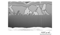
- the measurement of the average particle diameter of the copper crystal grains constituting the copper layer was obtained as follows. Using FIB-SIM, cut out five cross-sections, and in observing those cross-sections, in accordance with the cutting method of JIS H0501, draw a perpendicular connecting the insulator film surface and the copper surface at the center of the cross-section, The size of the hanging crystal was measured as the crystal grain size. The crystal grain size was measured at the five cross sections, and the average was taken as the average grain size of the copper crystal grains. Specifically, in the schematic diagram of the cross section by FIB-SIM shown in FIG.
- the length of the perpendicular line (1) drawn (intersecting) drawn at the center of the cross section is measured as the crystal grain size, and the same Then, the crystal grain size in a total of five cross sections was measured, and the average was determined as the average grain size. Further, the number of crystal grains occupying the surface from the surface on the insulator film side to the surface was also determined by observing the cross-sections at the five locations by FIB-SIM.
- the copper electrolyte of the present invention is added with a surfactant used for normal copper plating, such as polyethylene glycol. May be.
- a surfactant used for normal copper plating such as polyethylene glycol. May be.
- the two-layer flexible substrate of the present invention is obtained by providing a copper layer by electroplating on a substrate provided with a base metal layer using the above copper electrolyte. Plating is preferably performed at a bath temperature of 30 to 55 ° C, more preferably 35 to 45 ° C. Further, it is preferable to form a copper layer having a thickness of 3 to 18 ⁇ m.
- the MIT characteristic is more preferably 500 times or more.
- the two-layer flexible substrate produced using the copper electrolyte of the present invention has a large average grain size of 1 ⁇ m or more for the copper crystal grains constituting the copper layer, heat treatment during subsequent wiring, for example, COF lead There is no generation of Kirkendall voids even if heat treatment is performed after tin plating is performed on the part.
- Liquid volume 1700ml
- Anode Lead electrode
- Cathode Rotating electrode wound with a polyimide film having a base metal layer
- Polyimide film having a base metal layer 150kg of Ni-Cr on 37.5 ⁇ m thick Kapton E (made by DuPont)
- Cathode rotation speed 90 r. p. m.
- Copper ion 70 g / L
- Free sulfuric acid 60 g / L
- Comparative Example 8 The additive of the copper electrolyte solution in Example 1 was except that the chloride ion was 60 ppm, the commercially available additive Capre Grime 200A (manufactured by Nippon Leronal) was 0.4 mL / L, and the Capper Greme 200B (manufactured by Nippon Leronal) was 5 mL / L.
- the chloride ion was 60 ppm
- the commercially available additive Capre Grime 200A manufactured by Nippon Leronal
- the Capper Greme 200B manufactured by Nippon Leronal
- Copper grease 200A and copper grease 200B are commercially available additives for copper electrolytes for printed circuit boards.
- the obtained copper-coated polyimide bilayer substrate was evaluated as follows.
- the average grain size of the copper crystal grains constituting the copper layer and the number of crystal grains having the same size as the copper layer thickness within the range of 50 ⁇ m are obtained by cross-sectionally processing the obtained copper-coated polyimide bilayer substrate with FIB.
- the width was determined by observing a width of 50 ⁇ m with a scanning ion microscope.
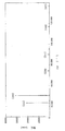
- FIG. 3 shows the XRD spectrum of the copper layer obtained in Example 3
- FIG. 4 shows the scanning ion microscope image of the cross section of the copper layer obtained in Example 6
- FIG. 4 shows the cross section of the copper layer obtained in Comparative Example 8.
- a scanning ion microscope image of is shown in FIG. In FIGS. 4 and 5, a part of the grain boundary is traced with a line for easy understanding of the grain boundary.
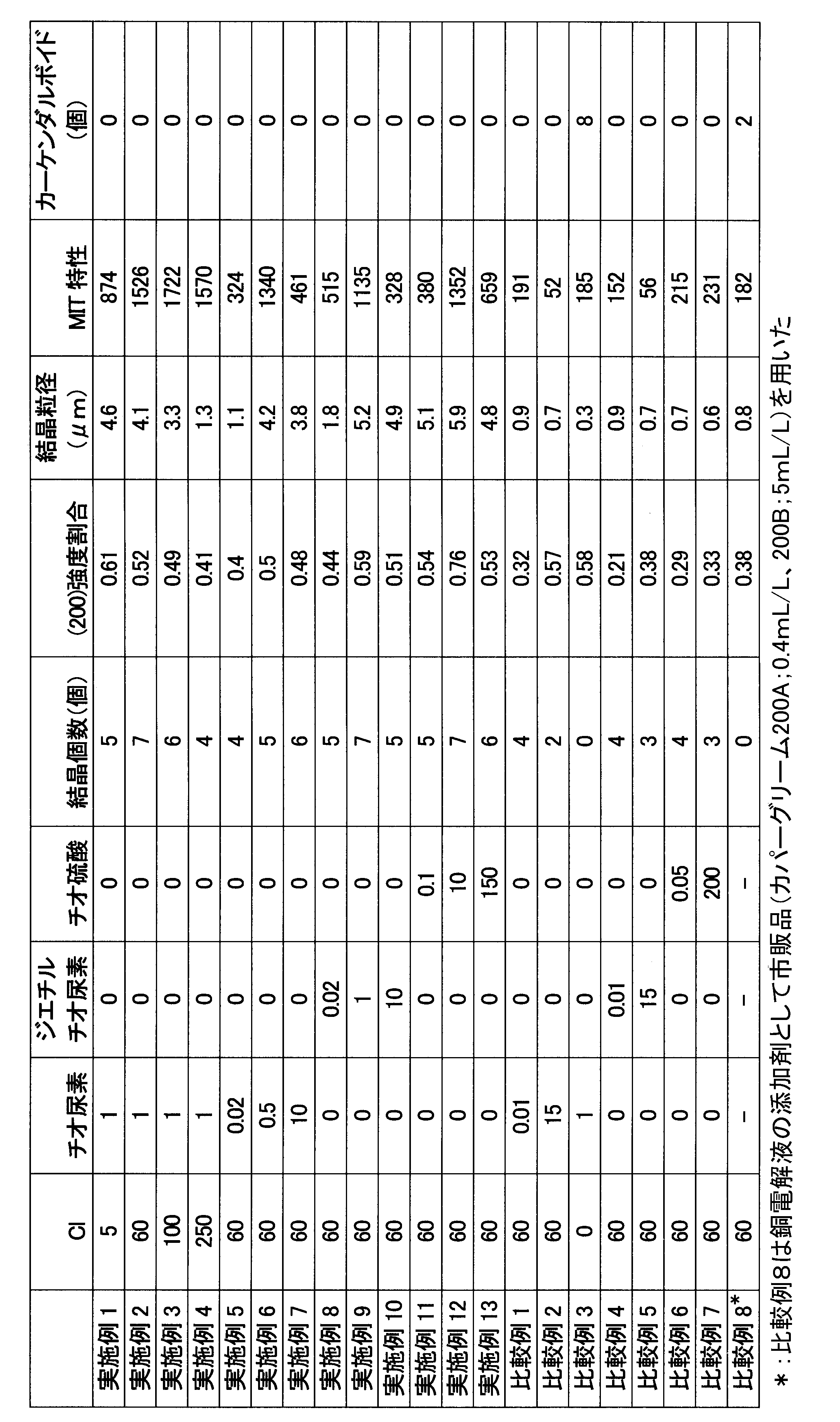
- Table 1 The results are shown in Table 1.
Landscapes
- Chemical & Material Sciences (AREA)
- Engineering & Computer Science (AREA)
- Metallurgy (AREA)
- Organic Chemistry (AREA)
- Materials Engineering (AREA)
- Electrochemistry (AREA)
- Chemical Kinetics & Catalysis (AREA)
- Crystallography & Structural Chemistry (AREA)
- Microelectronics & Electronic Packaging (AREA)
- Parts Printed On Printed Circuit Boards (AREA)
- Electroplating And Plating Baths Therefor (AREA)
- Laminated Bodies (AREA)
- Electroplating Methods And Accessories (AREA)
- Structure Of Printed Boards (AREA)
- Manufacturing Of Printed Wiring (AREA)
Abstract
Description
特に近年、二層フレキシブル基板において、多ピン化でリード部(COF(Chip on film)の接続部(インナーリード、アウターリード))が多くなり、ライン/スペース(ライン幅とスペース幅それぞれの幅、またはライン幅とスペース幅を合わせた幅)が狭くなって、配線ラインが細くなり、COFの実装時の折り曲げ時に断線する確率が高くなってきている。そのため、現状の耐折性よりも優れたものが要求されている。また、COFのリード部分にはスズめっきを行い、熱処理を実施する工程がある。銅層中に結晶粒径が数百nm程度の微細な結晶が存在すると、熱処理工程を実施することによって銅とスズとの拡散速度の違いにより、カーケンダルボイドと呼ばれる隙間を生じたり、スズ被膜が剥がれて、ショートの原因となる。そこでカーケンダルボイドが発生しない二層フレキシブル基板が要求されている。
本発明者らはさらに鋭意検討を行った結果、二層フレキシブル基板の銅層を構成する銅結晶粒の平均粒径を1μm以上とし、かつX線回折における(200)ピーク強度を高めることによりMIT特性が大きく改善することを見出し、また前記銅層は、電解液に特定の添加剤を使用することにより、形成できることを見出し、本発明に至った。
(1)絶縁体フィルムの片面又は両面上に、銅電解液を用いて銅層を設けた二層フレキシブル基板であって、前記銅層を構成する銅結晶粒の平均粒径が1μm以上、銅層の厚み以下であり、前記銅層がX線回折で(200)のピーク強度の主要6ピーク強度の和に対する比{(200)のピーク強度/((111)、(200)、(220)、(311)、(400)、(331)のピーク強度の和)}が0.4以上であることを特徴とする二層フレキシブル基板。
(2)前記銅層が、粒径が絶縁体フィルム側の面から銅層表面までを占める銅結晶粒を、基板面方向50μm視野内に4個以上含むことを特徴とする前記(1)記載の二層フレキシブル基板。
(3)絶縁体フィルム上にNi、Cr、Co、Ti、Cu、Mo、Si、Vの1種以上を含む下地金属層を設け、その下地金属層上に銅層を形成したことを特徴とする前記(1)又は(2)記載の二層フレキシブル基板。
(4)絶縁体フィルムがポリイミドフィルムであることを特徴とする前記(1)~(3)のいずれか一項に記載の二層フレキシブル基板。
(5)MIT特性が300回以上であることを特徴とする前記(1)~(4)のいずれか一項に記載の二層フレキシブル基板。
(6)前記(1)~(5)のいずれか一項に記載の二層フレキシブル基板の銅層を形成するための銅電解液であって、添加剤として、塩化物イオンと、チオ尿素、チオ尿素誘導体、チオ硫酸のいずれか1種もしくは2種以上とを含有することを特徴とする銅電解液。
(7)絶縁体フィルム上に、前記(6)記載の銅電解液を用いて銅層を形成することを特徴とする二層フレキシブル基板の製造方法。
絶縁体フィルムとしては、厚さ10~50μmのフィルムが好ましい。
下地金属層の厚さは10~500nmが好ましい。
銅電解液に用いる銅イオン源としては、硫酸銅、金属銅を硫酸で溶解した溶液等を用いることができる。銅電解液は、上記銅イオン源となる化合物の水溶液、又は金属銅を硫酸で溶解した溶液に添加剤を添加して用いる。銅電解液の銅濃度は、15~90g/Lが好ましく、硫酸濃度は50~200g/Lが好ましい。
本発明の銅電解液は、硫酸銅水溶液等の銅イオン源を含む水溶液に、塩化物イオン(Cl-)と、チオ尿素、チオ尿素誘導体、チオ硫酸のいずれか1種もしくは2種以上とを添加剤として含有させてなる。
銅電解液中の塩化物イオンは、例えば、NaCl、MgCl2、HCl等の塩化物イオンを含有する化合物を電解液中に溶解することにより含有させることができる。
チオ尿素誘導体としては、チオ尿素の水素原子が、低級アルキル基で置換された化合物が好ましく、テトラエチルチオ尿素(SC(N(C2H5)2)2)、テトラメチルチオ尿素、1,3-ジエチルチオ尿素(C2H5NHCSNHC2H5)、1,3-ジメチルチオ尿素等が挙げられる。
塩化物イオンが過剰であると、一般の銅箔の性状に近づき表面が荒れる。塩化物イオンが少ない場合は、結晶が微細になってMIT特性が悪くなる。チオ尿素、チオ尿素誘導体、チオ硫酸が好ましい濃度範囲外の場合、結晶粒径が小さくなり、MIT特性が悪くなる。
(200)ピーク強度の主要6ピーク強度の和に対する比は、0.5~0.8が好ましい。
また、粒径が絶縁体フィルム側の面から表面までを占める結晶粒の個数も、FIB-SIMによる前記5箇所の断面を観察し、その平均を求めた。
本発明の二層フレキシブル基板は、上記銅電解液を用い、下地金属層を設けた基板上に電気めっきにより銅層を設けたものである。めっきは、浴温30~55℃で行うことが好ましく、35~45℃がより好ましい。また、膜厚3~18μmの銅層を形成することが好ましい。
また、本発明の銅電解液を用いて作製された二層フレキシブル基板は、銅層を構成する銅結晶粒の平均粒径が1μm以上と大きいため、その後の配線時の熱処理、例えばCOFのリード部分にスズめっきを行った後の熱処理を施してもカーケンダルボイドの発生がない。
実施例1~13、比較例1~7
硫酸銅と硫酸を用い以下の濃度にした水溶液に添加剤を添加し、以下のめっき条件で下地金属層を有するポリイミドフィルムに電気めっきを行い、約8μmの銅被膜を作製した。めっき温度は40℃であり、添加剤及びその添加量は表1記載の通りである。尚、表1中、添加剤の添加量の単位はppmである。塩化物イオン源としては塩酸を用いた。
液容量: 1700ml
アノード:鉛電極
カソード:下地金属層を有するポリイミドフィルムを巻きつけた回転電極
下地金属層を有するポリイミドフィルム:
37.5μm厚のカプトンE(デュポン製)上にNi-Crを150Å
、更に銅を2000Åスパッタ成膜したもの
電流時間:2800As
電流密度:5→15→25→40A/dm2 この順番に35秒ずつ保持
カソード回転速度:90r.p.m.
銅イオン: 70g/L
フリーの硫酸:60g/L
実施例1における銅電解液の添加剤を、塩化物イオン60ppm、市販添加剤カパーグリーム200A(日本リーロナール製)を0.4mL/L、カパーグリーム200B(日本リーロナール製)を5mL/Lとした以外は実施例1と同様にして下地金属層を有するポリイミドフィルムに電気めっきを行い銅被膜ポリイミド二層基板を得た。カパーグリーム200A及びカパーグリーム200Bはプリント基板用の銅電解液用に市販されている添加剤である。
(1)MIT特性
MIT試験片は、得られた銅被覆ポリイミド二層基板に、一般的な液状レジスト塗布、露光、現像、エッチングにより、ライン幅200μmの配線パターンを形成した図2に示すものを用いて、JIS C 5016に基づいて、加重500g、R=0.8にて測定した。
得られた銅被覆ポリイミド二層基板に、一般的な液状レジスト塗布、露光、現像、エッチングにより、図2に示すパターンにおいてライン幅を50μmとした以外は同様に配線パターンを形成した回路に市販のスズめっき液(石原薬品製)によりスズめっきした後、150℃、1時間の熱処理をしたサンプルについて、配線パターンの配線幅方向にFIB(集束イオンビーム加工装置)で断面加工して、図6に示すように、ライン断面全体に存在するカーケンダルボイドの発生個数を求めた。
実施例3で得られた銅層のXRDスペクトルを図3に、実施例6で得られた銅層の断面の走査型イオン顕微鏡像を図4に、比較例8で得られた銅層の断面の走査型イオン顕微鏡像を図5に示す。尚、図4、図5においては、粒界を分かり易くするため、粒界の一部を線でなぞって示した。
結果は表1に示す。
Claims (7)
- 絶縁体フィルムの片面又は両面上に、銅電解液を用いて銅層を設けた二層フレキシブル基板であって、前記銅層を構成する銅結晶粒の平均粒径が1μm以上、銅層の厚み以下であり、前記銅層がX線回折で(200)ピーク強度の主要6ピーク強度の和に対する比{(200)のピーク強度/((111)、(200)、(220)、(311)、(400)、(331)のピーク強度の和)}が0.4以上であることを特徴とする二層フレキシブル基板。
- 前記銅層が、粒径が絶縁体フィルム側の面から銅層表面までを占める銅結晶粒を、基板面方向50μm範囲内に4個以上含むことを特徴とする請求項1記載の二層フレキシブル基板。
- 絶縁体フィルム上にNi、Cr、Co、Ti、Cu、Mo、Si、Vの1種以上を含む下地金属層を設け、その下地金属層上に銅層を形成したことを特徴とする請求項1又は2記載の二層フレキシブル基板。
- 絶縁体フィルムがポリイミドフィルムであることを特徴とする請求項1~3のいずれか一項に記載の二層フレキシブル基板。
- MIT特性が300回以上であることを特徴とする請求項1~4のいずれか一項に記載の二層フレキシブル基板。
- 請求項1~5のいずれか一項に記載の二層フレキシブル基板の銅層を形成するための銅電解液であって、添加剤として、塩化物イオンと、チオ尿素、チオ尿素誘導体、チオ硫酸のいずれか1種もしくは2種以上とを含有することを特徴とする銅電解液。
- 絶縁体フィルム上に、請求項6記載の銅電解液を用いて銅層を形成することを特徴とする二層フレキシブル基板の製造方法。
Priority Applications (4)
| Application Number | Priority Date | Filing Date | Title |
|---|---|---|---|
| US13/138,535 US20110311834A1 (en) | 2009-03-23 | 2010-03-23 | Two-layer flexible substrate, and copper electrolytic solution for producing same |
| JP2011506058A JPWO2010110259A1 (ja) | 2009-03-23 | 2010-03-23 | 二層フレキシブル基板、及びその製造に用いる銅電解液 |
| KR1020117022927A KR101339598B1 (ko) | 2009-03-23 | 2010-03-23 | 2층 플렉시블 기판, 및 그 제조에 이용하는 구리전해액 |
| CN2010800112670A CN102348835A (zh) | 2009-03-23 | 2010-03-23 | 双层挠性基板、和在其制造中使用的铜电解液 |
Applications Claiming Priority (2)
| Application Number | Priority Date | Filing Date | Title |
|---|---|---|---|
| JP2009070361 | 2009-03-23 | ||
| JP2009-070361 | 2009-03-23 |
Publications (1)
| Publication Number | Publication Date |
|---|---|
| WO2010110259A1 true WO2010110259A1 (ja) | 2010-09-30 |
Family
ID=42780952
Family Applications (1)
| Application Number | Title | Priority Date | Filing Date |
|---|---|---|---|
| PCT/JP2010/054974 Ceased WO2010110259A1 (ja) | 2009-03-23 | 2010-03-23 | 二層フレキシブル基板、及びその製造に用いる銅電解液 |
Country Status (6)
| Country | Link |
|---|---|
| US (1) | US20110311834A1 (ja) |
| JP (1) | JPWO2010110259A1 (ja) |
| KR (1) | KR101339598B1 (ja) |
| CN (1) | CN102348835A (ja) |
| TW (1) | TW201037105A (ja) |
| WO (1) | WO2010110259A1 (ja) |
Cited By (8)
| Publication number | Priority date | Publication date | Assignee | Title |
|---|---|---|---|---|
| WO2011136061A1 (ja) * | 2010-04-30 | 2011-11-03 | Jx日鉱日石金属株式会社 | フレキシブル配線用積層体 |
| JP2013019037A (ja) * | 2011-07-13 | 2013-01-31 | Sumitomo Metal Mining Co Ltd | 銅電気めっき方法及びその銅電気めっき方法を用いて成膜された銅めっき被膜を有する金属化樹脂フィルム |
| WO2014119355A1 (ja) * | 2013-01-29 | 2014-08-07 | 古河電気工業株式会社 | 電解銅箔及びその製造方法 |
| JP2015140447A (ja) * | 2014-01-27 | 2015-08-03 | 住友金属鉱山株式会社 | フレキシブル配線板 |
| CN113046796A (zh) * | 2019-12-27 | 2021-06-29 | 铂识科技股份有限公司 | 一种纳米双晶层的制备方法和一种纳米双晶层 |
| JP2022020606A (ja) * | 2020-07-20 | 2022-02-01 | トーレ・アドバンスド・マテリアルズ・コリア・インコーポレーテッド | 軟性銅箔積層フィルム、及びそれを含む電気素子 |
| JP2023081865A (ja) * | 2021-12-01 | 2023-06-13 | トーレ・アドバンスド・マテリアルズ・コリア・インコーポレーテッド | 軟性銅箔積層フィルム、その製造方法、及びそれを含む電気素子 |
| JP2023103401A (ja) * | 2019-07-04 | 2023-07-26 | 住友電気工業株式会社 | プリント配線板及びその製造方法 |
Families Citing this family (19)
| Publication number | Priority date | Publication date | Assignee | Title |
|---|---|---|---|---|
| JP6398596B2 (ja) * | 2013-10-22 | 2018-10-03 | 住友金属鉱山株式会社 | 2層フレキシブル配線用基板及びそれを用いたフレキシブル配線板 |
| TWI568865B (zh) * | 2013-10-23 | 2017-02-01 | Sumitomo Metal Mining Co | Layer 2 flexible wiring substrate and manufacturing method thereof, and two-layer flexible wiring board and manufacturing method thereof |
| TWI542739B (zh) * | 2014-03-21 | 2016-07-21 | 長春石油化學股份有限公司 | 電解銅箔 |
| CN104328464A (zh) * | 2014-12-02 | 2015-02-04 | 深圳市博敏电子有限公司 | 一种线路板镀铜液及镀铜方法 |
| JP6782561B2 (ja) | 2015-07-16 | 2020-11-11 | Jx金属株式会社 | キャリア付銅箔、積層体、積層体の製造方法、プリント配線板の製造方法及び電子機器の製造方法 |
| JP6006445B1 (ja) | 2015-07-27 | 2016-10-12 | Jx金属株式会社 | キャリア付銅箔、積層体、プリント配線板の製造方法及び電子機器の製造方法 |
| JP6058182B1 (ja) * | 2015-07-27 | 2017-01-11 | Jx金属株式会社 | キャリア付銅箔、積層体、プリント配線板の製造方法及び電子機器の製造方法 |
| JP6200042B2 (ja) | 2015-08-06 | 2017-09-20 | Jx金属株式会社 | キャリア付銅箔、積層体、プリント配線板の製造方法及び電子機器の製造方法 |
| JP6190500B2 (ja) | 2015-08-06 | 2017-08-30 | Jx金属株式会社 | キャリア付銅箔、積層体、プリント配線板の製造方法及び電子機器の製造方法 |
| JP6339636B2 (ja) | 2015-08-06 | 2018-06-06 | Jx金属株式会社 | キャリア付銅箔、積層体、プリント配線板の製造方法及び電子機器の製造方法 |
| DE102015224464A1 (de) | 2015-12-07 | 2017-06-08 | Aurubis Stolberg Gmbh & Co. Kg | Kupfer-Keramik-Substrat, Kupferhalbzeug zur Herstellung eines Kupfer-Keramik-Substrats und Verfahren zur Herstellung eines Kupfer-Keramik-Substrats |
| US9673646B1 (en) * | 2016-08-19 | 2017-06-06 | Chang Chun Petrochemical Co., Ltd. | Surface-treated electrolytic copper foil and method for wireless charging of flexible printed circuit board |
| JP6222318B2 (ja) * | 2016-09-07 | 2017-11-01 | 大日本印刷株式会社 | Led用リードフレームまたは基板およびその製造方法、ならびに半導体装置およびその製造方法 |
| KR102093497B1 (ko) | 2018-07-11 | 2020-03-26 | 삼성디스플레이 주식회사 | 표시모듈 및 이를 포함하는 표시장치 |
| TWI731330B (zh) * | 2019-04-30 | 2021-06-21 | 南亞塑膠工業股份有限公司 | 電解銅箔、其製造方法、及鋰離子二次電池 |
| TWI825562B (zh) * | 2021-01-20 | 2023-12-11 | 南韓商東麗先端素材股份有限公司 | 覆銅層壓膜、包括其的電子元件以及所述覆銅層壓膜的製造方法 |
| CN113068313A (zh) * | 2021-03-05 | 2021-07-02 | 江西展耀微电子有限公司 | 一种线路板的制作方法及其制作的线路板、电子设备 |
| KR102469768B1 (ko) * | 2021-10-26 | 2022-11-22 | 도레이첨단소재 주식회사 | 동박적층필름 및 이를 포함하는 전자소자 |
| WO2023117127A1 (en) * | 2021-12-24 | 2023-06-29 | Circuit Foil Luxembourg | Electrolytic copper foil and secondary battery comprising the same |
Citations (2)
| Publication number | Priority date | Publication date | Assignee | Title |
|---|---|---|---|---|
| JPH07207490A (ja) * | 1994-01-19 | 1995-08-08 | Sumitomo Metal Mining Co Ltd | 電気銅めっき液 |
| JP2006316328A (ja) * | 2005-05-16 | 2006-11-24 | Daiso Co Ltd | 2層フレキシブル銅張積層板の製造方法 |
Family Cites Families (3)
| Publication number | Priority date | Publication date | Assignee | Title |
|---|---|---|---|---|
| JPS54145965A (en) * | 1978-05-08 | 1979-11-14 | Nippon Mining Co | Method of and apparatus for producing board for printed circuit |
| JP2005142387A (ja) * | 2003-11-07 | 2005-06-02 | Nippon Mektron Ltd | 可撓性回路基板 |
| JP4804806B2 (ja) * | 2005-06-13 | 2011-11-02 | 新日鐵化学株式会社 | 銅張積層板及びその製造方法 |
-
2010
- 2010-03-22 TW TW099108294A patent/TW201037105A/zh unknown
- 2010-03-23 WO PCT/JP2010/054974 patent/WO2010110259A1/ja not_active Ceased
- 2010-03-23 JP JP2011506058A patent/JPWO2010110259A1/ja active Pending
- 2010-03-23 KR KR1020117022927A patent/KR101339598B1/ko not_active Expired - Fee Related
- 2010-03-23 US US13/138,535 patent/US20110311834A1/en not_active Abandoned
- 2010-03-23 CN CN2010800112670A patent/CN102348835A/zh active Pending
Patent Citations (2)
| Publication number | Priority date | Publication date | Assignee | Title |
|---|---|---|---|---|
| JPH07207490A (ja) * | 1994-01-19 | 1995-08-08 | Sumitomo Metal Mining Co Ltd | 電気銅めっき液 |
| JP2006316328A (ja) * | 2005-05-16 | 2006-11-24 | Daiso Co Ltd | 2層フレキシブル銅張積層板の製造方法 |
Cited By (11)
| Publication number | Priority date | Publication date | Assignee | Title |
|---|---|---|---|---|
| WO2011136061A1 (ja) * | 2010-04-30 | 2011-11-03 | Jx日鉱日石金属株式会社 | フレキシブル配線用積層体 |
| JPWO2011136061A1 (ja) * | 2010-04-30 | 2013-07-18 | Jx日鉱日石金属株式会社 | フレキシブル配線用積層体 |
| JP2013019037A (ja) * | 2011-07-13 | 2013-01-31 | Sumitomo Metal Mining Co Ltd | 銅電気めっき方法及びその銅電気めっき方法を用いて成膜された銅めっき被膜を有する金属化樹脂フィルム |
| WO2014119355A1 (ja) * | 2013-01-29 | 2014-08-07 | 古河電気工業株式会社 | 電解銅箔及びその製造方法 |
| JP2015140447A (ja) * | 2014-01-27 | 2015-08-03 | 住友金属鉱山株式会社 | フレキシブル配線板 |
| JP2023103401A (ja) * | 2019-07-04 | 2023-07-26 | 住友電気工業株式会社 | プリント配線板及びその製造方法 |
| JP7597147B2 (ja) | 2019-07-04 | 2024-12-10 | 住友電気工業株式会社 | プリント配線板及びその製造方法 |
| CN113046796A (zh) * | 2019-12-27 | 2021-06-29 | 铂识科技股份有限公司 | 一种纳米双晶层的制备方法和一种纳米双晶层 |
| JP2022020606A (ja) * | 2020-07-20 | 2022-02-01 | トーレ・アドバンスド・マテリアルズ・コリア・インコーポレーテッド | 軟性銅箔積層フィルム、及びそれを含む電気素子 |
| JP7189284B2 (ja) | 2020-07-20 | 2022-12-13 | トーレ・アドバンスド・マテリアルズ・コリア・インコーポレーテッド | 軟性銅箔積層フィルム、及びそれを含む電気素子 |
| JP2023081865A (ja) * | 2021-12-01 | 2023-06-13 | トーレ・アドバンスド・マテリアルズ・コリア・インコーポレーテッド | 軟性銅箔積層フィルム、その製造方法、及びそれを含む電気素子 |
Also Published As
| Publication number | Publication date |
|---|---|
| KR101339598B1 (ko) | 2013-12-10 |
| CN102348835A (zh) | 2012-02-08 |
| US20110311834A1 (en) | 2011-12-22 |
| TW201037105A (en) | 2010-10-16 |
| KR20110132421A (ko) | 2011-12-07 |
| JPWO2010110259A1 (ja) | 2012-09-27 |
Similar Documents
| Publication | Publication Date | Title |
|---|---|---|
| WO2010110259A1 (ja) | 二層フレキシブル基板、及びその製造に用いる銅電解液 | |
| TWI434965B (zh) | A roughening method for copper foil, and a copper foil for a printed wiring board which is obtained by the roughening method | |
| JP5654416B2 (ja) | 液晶ポリマー銅張積層板及び当該積層板に用いる銅箔 | |
| CN101636527B (zh) | 铜电解液和使用该铜电解液得到的两层挠性基板 | |
| TWI406614B (zh) | 印刷配線基板及其製造方法 | |
| TWI514937B (zh) | 佈線電路基板 | |
| JP2016168687A (ja) | 複合金属箔及びその製造方法並びにプリント配線板 | |
| JP2001181886A (ja) | 電解銅箔 | |
| JP4924843B2 (ja) | 2層フレキシブル基板及びその製造方法、並びに、該2層フレキシブル基板を用いたプリント配線基板及びその製造方法 | |
| JP7193133B2 (ja) | 配線基板 | |
| JP2006052441A (ja) | 銅箔及びその製造方法、並びにtabテープ | |
| JP4540100B2 (ja) | 2層フレキシブル銅張積層板及びその2層フレキシブル銅張積層板の製造方法 | |
| JP4345742B2 (ja) | 配線基板及びその製造方法 | |
| JP4430020B2 (ja) | フレキシブルプリント配線板用銅箔、その製造方法及びフレキシブルプリント配線板 | |
| CN103476198B (zh) | 印刷电路板用铜箔及其制法以及使用该铜箔的印刷电路板 | |
| JP2012186307A (ja) | 2層フレキシブル基板とその製造方法、並びに2層フレキシブル基板を基材とした2層フレキシブルプリント配線板と、その製造方法 | |
| JP4872257B2 (ja) | 2層めっき基板およびその製造方法 | |
| CN114901873A (zh) | 电解铜箔 | |
| JP5255496B2 (ja) | 金属張積層体及び金属張積層体の製造方法 | |
| WO2018193940A1 (ja) | 導電性基板 | |
| WO2021200614A1 (ja) | フレキシブルプリント配線板及びその製造方法 | |
| TWI765021B (zh) | 導電性基板、導電性基板之製造方法 | |
| JP2020145338A (ja) | 配線基板 | |
| JP2008091596A (ja) | 表面平滑性を有する銅被覆ポリイミド基板とその製造方法 |
Legal Events
| Date | Code | Title | Description |
|---|---|---|---|
| WWE | Wipo information: entry into national phase |
Ref document number: 201080011267.0 Country of ref document: CN |
|
| 121 | Ep: the epo has been informed by wipo that ep was designated in this application |
Ref document number: 10756055 Country of ref document: EP Kind code of ref document: A1 |
|
| WWE | Wipo information: entry into national phase |
Ref document number: 2011506058 Country of ref document: JP |
|
| WWE | Wipo information: entry into national phase |
Ref document number: 13138535 Country of ref document: US |
|
| NENP | Non-entry into the national phase |
Ref country code: DE |
|
| ENP | Entry into the national phase |
Ref document number: 20117022927 Country of ref document: KR Kind code of ref document: A |
|
| 122 | Ep: pct application non-entry in european phase |
Ref document number: 10756055 Country of ref document: EP Kind code of ref document: A1 |