WO2010100705A1 - 半導体装置及びその製造方法 - Google Patents
半導体装置及びその製造方法 Download PDFInfo
- Publication number
- WO2010100705A1 WO2010100705A1 PCT/JP2009/007346 JP2009007346W WO2010100705A1 WO 2010100705 A1 WO2010100705 A1 WO 2010100705A1 JP 2009007346 W JP2009007346 W JP 2009007346W WO 2010100705 A1 WO2010100705 A1 WO 2010100705A1
- Authority
- WO
- WIPO (PCT)
- Prior art keywords
- film
- semiconductor device
- insulating
- insulating film
- via hole
- Prior art date
- Legal status (The legal status is an assumption and is not a legal conclusion. Google has not performed a legal analysis and makes no representation as to the accuracy of the status listed.)
- Ceased
Links
Images


Classifications
-
- H—ELECTRICITY
- H10—SEMICONDUCTOR DEVICES; ELECTRIC SOLID-STATE DEVICES NOT OTHERWISE PROVIDED FOR
- H10W—GENERIC PACKAGES, INTERCONNECTIONS, CONNECTORS OR OTHER CONSTRUCTIONAL DETAILS OF DEVICES COVERED BY CLASS H10
- H10W20/00—Interconnections in chips, wafers or substrates
- H10W20/01—Manufacture or treatment
- H10W20/021—Manufacture or treatment of interconnections within wafers or substrates
- H10W20/023—Manufacture or treatment of interconnections within wafers or substrates the interconnections being through-semiconductor vias
- H10W20/0234—Manufacture or treatment of interconnections within wafers or substrates the interconnections being through-semiconductor vias comprising etching via holes that stop on pads or on electrodes
-
- H—ELECTRICITY
- H10—SEMICONDUCTOR DEVICES; ELECTRIC SOLID-STATE DEVICES NOT OTHERWISE PROVIDED FOR
- H10W—GENERIC PACKAGES, INTERCONNECTIONS, CONNECTORS OR OTHER CONSTRUCTIONAL DETAILS OF DEVICES COVERED BY CLASS H10
- H10W20/00—Interconnections in chips, wafers or substrates
- H10W20/01—Manufacture or treatment
- H10W20/021—Manufacture or treatment of interconnections within wafers or substrates
- H10W20/023—Manufacture or treatment of interconnections within wafers or substrates the interconnections being through-semiconductor vias
- H10W20/0242—Manufacture or treatment of interconnections within wafers or substrates the interconnections being through-semiconductor vias comprising etching via holes from the back sides of the chips, wafers or substrates
-
- H—ELECTRICITY
- H10—SEMICONDUCTOR DEVICES; ELECTRIC SOLID-STATE DEVICES NOT OTHERWISE PROVIDED FOR
- H10W—GENERIC PACKAGES, INTERCONNECTIONS, CONNECTORS OR OTHER CONSTRUCTIONAL DETAILS OF DEVICES COVERED BY CLASS H10
- H10W20/00—Interconnections in chips, wafers or substrates
- H10W20/01—Manufacture or treatment
- H10W20/021—Manufacture or treatment of interconnections within wafers or substrates
- H10W20/023—Manufacture or treatment of interconnections within wafers or substrates the interconnections being through-semiconductor vias
- H10W20/0249—Manufacture or treatment of interconnections within wafers or substrates the interconnections being through-semiconductor vias wherein the through-semiconductor via protrudes from backsides of the chips, wafers or substrates during the manufacture
-
- H—ELECTRICITY
- H10—SEMICONDUCTOR DEVICES; ELECTRIC SOLID-STATE DEVICES NOT OTHERWISE PROVIDED FOR
- H10W—GENERIC PACKAGES, INTERCONNECTIONS, CONNECTORS OR OTHER CONSTRUCTIONAL DETAILS OF DEVICES COVERED BY CLASS H10
- H10W20/00—Interconnections in chips, wafers or substrates
- H10W20/01—Manufacture or treatment
- H10W20/021—Manufacture or treatment of interconnections within wafers or substrates
- H10W20/023—Manufacture or treatment of interconnections within wafers or substrates the interconnections being through-semiconductor vias
- H10W20/0265—Manufacture or treatment of interconnections within wafers or substrates the interconnections being through-semiconductor vias characterised by the sidewall insulation
-
- H—ELECTRICITY
- H10—SEMICONDUCTOR DEVICES; ELECTRIC SOLID-STATE DEVICES NOT OTHERWISE PROVIDED FOR
- H10W—GENERIC PACKAGES, INTERCONNECTIONS, CONNECTORS OR OTHER CONSTRUCTIONAL DETAILS OF DEVICES COVERED BY CLASS H10
- H10W20/00—Interconnections in chips, wafers or substrates
- H10W20/20—Interconnections within wafers or substrates, e.g. through-silicon vias [TSV]
- H10W20/211—Through-semiconductor vias, e.g. TSVs
- H10W20/213—Cross-sectional shapes or dispositions
- H10W20/2134—TSVs extending from the semiconductor wafer into back-end-of-line layers
-
- H—ELECTRICITY
- H10—SEMICONDUCTOR DEVICES; ELECTRIC SOLID-STATE DEVICES NOT OTHERWISE PROVIDED FOR
- H10W—GENERIC PACKAGES, INTERCONNECTIONS, CONNECTORS OR OTHER CONSTRUCTIONAL DETAILS OF DEVICES COVERED BY CLASS H10
- H10W20/00—Interconnections in chips, wafers or substrates
- H10W20/20—Interconnections within wafers or substrates, e.g. through-silicon vias [TSV]
- H10W20/211—Through-semiconductor vias, e.g. TSVs
- H10W20/217—Through-semiconductor vias, e.g. TSVs comprising ring-shaped isolation structures outside of the via holes
-
- H—ELECTRICITY
- H10—SEMICONDUCTOR DEVICES; ELECTRIC SOLID-STATE DEVICES NOT OTHERWISE PROVIDED FOR
- H10W—GENERIC PACKAGES, INTERCONNECTIONS, CONNECTORS OR OTHER CONSTRUCTIONAL DETAILS OF DEVICES COVERED BY CLASS H10
- H10W90/00—Package configurations
-
- H—ELECTRICITY
- H10—SEMICONDUCTOR DEVICES; ELECTRIC SOLID-STATE DEVICES NOT OTHERWISE PROVIDED FOR
- H10W—GENERIC PACKAGES, INTERCONNECTIONS, CONNECTORS OR OTHER CONSTRUCTIONAL DETAILS OF DEVICES COVERED BY CLASS H10
- H10W90/00—Package configurations
- H10W90/20—Configurations of stacked chips
- H10W90/28—Configurations of stacked chips the stacked chips having different sizes, e.g. chip stacks having a pyramidal shape
-
- H—ELECTRICITY
- H10—SEMICONDUCTOR DEVICES; ELECTRIC SOLID-STATE DEVICES NOT OTHERWISE PROVIDED FOR
- H10W—GENERIC PACKAGES, INTERCONNECTIONS, CONNECTORS OR OTHER CONSTRUCTIONAL DETAILS OF DEVICES COVERED BY CLASS H10
- H10W90/00—Package configurations
- H10W90/20—Configurations of stacked chips
- H10W90/297—Configurations of stacked chips characterised by the through-semiconductor vias [TSVs] in the stacked chips
-
- H—ELECTRICITY
- H10—SEMICONDUCTOR DEVICES; ELECTRIC SOLID-STATE DEVICES NOT OTHERWISE PROVIDED FOR
- H10W—GENERIC PACKAGES, INTERCONNECTIONS, CONNECTORS OR OTHER CONSTRUCTIONAL DETAILS OF DEVICES COVERED BY CLASS H10
- H10W90/00—Package configurations
- H10W90/701—Package configurations characterised by the relative positions of pads or connectors relative to package parts
- H10W90/721—Package configurations characterised by the relative positions of pads or connectors relative to package parts of bump connectors
- H10W90/722—Package configurations characterised by the relative positions of pads or connectors relative to package parts of bump connectors between stacked chips
-
- H—ELECTRICITY
- H10—SEMICONDUCTOR DEVICES; ELECTRIC SOLID-STATE DEVICES NOT OTHERWISE PROVIDED FOR
- H10W—GENERIC PACKAGES, INTERCONNECTIONS, CONNECTORS OR OTHER CONSTRUCTIONAL DETAILS OF DEVICES COVERED BY CLASS H10
- H10W90/00—Package configurations
- H10W90/701—Package configurations characterised by the relative positions of pads or connectors relative to package parts
- H10W90/721—Package configurations characterised by the relative positions of pads or connectors relative to package parts of bump connectors
- H10W90/724—Package configurations characterised by the relative positions of pads or connectors relative to package parts of bump connectors between a chip and a stacked insulating package substrate, interposer or RDL
Definitions
- the present invention relates to a semiconductor device in which semiconductor integrated circuits are three-dimensionally integrated with through vias and a method for manufacturing the same.
- Non-Patent Document 1 a method for manufacturing a through silicon via according to a conventional example will be described with reference to the disclosure of Non-Patent Document 1.
- 13 (a) to 13 (f) are cross-sectional views showing respective steps of a method for manufacturing a through silicon via according to a conventional example.
- the back surface of the silicon substrate 101 (opposite surface of the device side surface) side. Polishing is performed to reduce the thickness of the silicon substrate 101 to about 50 ⁇ m.
- FIG. 13B shows a plan view of the ring-shaped groove 151.
- an insulating polymer 107 is applied on the back surface of the silicon substrate 101 to embed a ring-shaped groove 151.
- a resist 108 having an opening on a circular region surrounded by the ring-shaped groove 151 is formed on the insulating polymer 107 by a lithography method, and then the resist 108 is masked. Then, the insulating polymer 107 is etched. As a result, the portion of the insulating polymer 107 located in the circular region surrounded by the ring-shaped groove 151 is removed.
- a portion of the silicon substrate 101 located in a circular region surrounded by the ring-shaped groove 151 is removed by dry etching, thereby forming a via hole 152 reaching the interlayer film 102. .
- the interlayer film 102 at the bottom of the via hole 152 is removed by wet etching. As a result, the wiring 103 formed on the interlayer film 102 covering the device side surface of the silicon substrate 101 is exposed.
- a seed layer 109 is formed so as to cover the wall surface and bottom surface of the via hole 152, and then a resist pattern 110 having an opening in the wiring formation region is formed.
- copper plating is performed to fill the via hole 152 with the copper film 111.
- the resist pattern 110 and the seed layer 109 below the resist pattern 110 are removed to complete the through silicon via electrode.
- the insulating polymer 107 having a lower dielectric constant and lower elastic modulus than the insulating film formed by CVD (chemical vapor deposition) is applied to the silicon substrate 101 and the through via (copper copper).
- the parasitic capacitance due to the through via can be reduced.
- the insulating polymer 107 serves as a buffer material, it is possible to alleviate stress mismatch caused by the difference in thermal expansion coefficient between the silicon substrate 101 and the through via (copper film 111).
- the present invention provides a semiconductor device in which a semiconductor integrated circuit is three-dimensionally integrated with through vias, while reducing the parasitic capacitance caused by the through vias while achieving miniaturization, high integration, and low cost.
- An object is to improve the reliability by making it possible to alleviate the stress mismatch caused by the difference in thermal expansion coefficient between the substrate material and the through via material.
- a method of manufacturing a semiconductor device penetrates a semiconductor substrate having a first surface serving as an element formation surface and a second surface opposite to the first surface.
- the method further includes the step of forming an insulating protective film on the second surface of the semiconductor substrate before the step (a), and in the step (a) The via hole is formed so as to further penetrate the protective film, and is embedded in the via hole in a portion located in the protective film between the step (b) and the step (c).
- the via coating material remaining in the via hole may be etched.
- the insulating film may be made of a material that is harder to etch than the via coating material.
- the method further includes the step of forming an insulating protective film on the second surface of the semiconductor substrate before the step (a), and in the step (a)
- the via hole is formed so as to further penetrate the protective film, and in the step (c), the via coating material is also used as the via coating film on the inner wall of the via hole at a portion located in the protective film. It may be left.
- the via coating material is formed even on the protective film, and in the step (c), the via coating material is also left as the via coating film on the protective film. May be.
- the via coating material may be made of an insulating polymer.
- a semiconductor device includes a semiconductor substrate having a first surface serving as an element formation surface and a second surface opposite to the first surface, a through via penetrating the semiconductor substrate, and the through via An insulating via coating film formed between the sidewall of the semiconductor substrate and the semiconductor substrate; and an insulating protective film formed on the second surface of the semiconductor substrate;
- the protective film is an insulating film different from each other.
- an end of the via coating film on the second surface side is located in substantially the same plane as the second surface of the semiconductor substrate, An insulating film different from the protective film may be formed so as to cover the end on the second surface side.
- the end of the via coating film on the second surface side may be located in substantially the same plane as the surface of the protective film.
- the via coating film may be formed even on the protective film.
- the via coating film may be made of an insulating polymer.
- a via coating film having a low dielectric constant can be formed thinly in a self-aligned manner on the side wall of the through via, thereby reducing the parasitic capacitance caused by the through via. can do.
- the via coating film having a low elastic modulus functions as a buffer material, stress mismatch due to the difference in thermal expansion coefficient between the substrate material and the through via material can be reduced. Accordingly, a semiconductor device in which a semiconductor integrated circuit is three-dimensionally integrated with a highly reliable through via can be provided at low cost, and further miniaturization and high integration of the semiconductor device can be realized. .
- FIG. 1A to FIG. 1H are cross-sectional views showing respective steps of a semiconductor device manufacturing method according to the first embodiment of the present invention.
- FIG. 2 is a cross-sectional view of the semiconductor device according to the first embodiment of the present invention.
- FIG. 3A to FIG. 3H are cross-sectional views showing respective steps of a method for manufacturing a semiconductor device according to a first modification of the first embodiment of the present invention.
- FIG. 4 is a cross-sectional view of a semiconductor device according to a first modification of the first embodiment of the present invention.
- FIG. 5A to FIG. 5H are cross-sectional views showing respective steps of the method for manufacturing the semiconductor device according to the second modification of the first embodiment.
- FIG. 6 is a cross-sectional view of a semiconductor device according to a second modification of the first embodiment.
- FIG. 7A to FIG. 7G are cross-sectional views showing the respective steps of the semiconductor device manufacturing method according to the third modification of the first embodiment.
- FIG. 8 is a cross-sectional view of a semiconductor device according to a third modification of the first embodiment.
- FIG. 9 is a cross-sectional view showing an example of a structure according to the second embodiment of the present invention.
- FIG. 10 is a cross-sectional view showing an example of a structure according to the second embodiment of the present invention.
- FIG. 11 is a cross-sectional view showing an example of a structure according to the second embodiment of the present invention.
- FIG. 12 is a cross-sectional view showing an example of a structure according to the second embodiment of the present invention.
- 13A to 13F are cross-sectional views showing respective steps of a semiconductor device manufacturing method according to a conventional example.
- FIG. 14 is a top view at the time when the step shown in FIG. 13B of the semiconductor device manufacturing method according to the conventional example is completed.
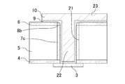
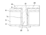
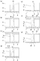
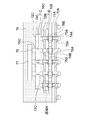
- the device-side surface of a silicon device wafer (for example, a semiconductor substrate such as a silicon substrate) 5 is attached to a glass carrier 1 with wax 2, and then the device-side surface is face-downed.
- the silicon device wafer 5 is polished from the back surface (opposite surface of the device side surface), and is thinned to a thickness of about 50 ⁇ m, for example.
- a first insulating film (surface protective film) 4 is formed on the device side surface of the silicon device wafer 5, and a metal film serving as a wiring or a pad is formed on the surface of the first insulating film 4. 3 is formed.
- the metal film 3 may be formed inside the first insulating film 4, but for the sake of simplicity, the metal film 3 is formed on the surface of the first insulating film 4. A state in which the film 3 is formed is illustrated.
- the glass carrier 1 is a tool for handling the silicon device wafer 5.
- a second insulating film (back surface protective film) 6 having a thickness of about 1 ⁇ m made of, for example, a silicon nitride (SiN) film is formed on the back surface of the polished silicon device wafer 5, and then the second insulating film 6. Further, a via hole 21 having a via diameter of 10 ⁇ m, for example, penetrating the silicon device wafer 5 is formed so as to reach the first insulating film 4.
- the via hole 21 fills the second insulating film 6 including the inside of the via hole 21 with a third insulating film 7 a made of, for example, an insulating polymer and having a thickness of about 5 ⁇ m. accumulate.
- a portion of the third insulating film 7 a located on the second insulating film 6 and a portion of the via hole 21 located in the second insulating film 6 are formed.
- the third insulating film 7a is removed, and a dummy plug 7b made of the third insulating film 7a is formed.
- the dummy plug 7b and the second insulating film 6 for example, a thickness of about 1 ⁇ m having an etching selectivity with respect to the third insulating film 7a (that is, the dummy plug 7b).
- the fourth insulating film 8a is formed.
- anisotropic etching back is performed on the fourth insulating film 8 a, so that a portion of the inner wall of the via hole 21 located in the second insulating film 6 is formed on the second wall.
- a side wall 8b made of four insulating films 8a is formed.
- the dummy plug 7 b and the first insulating film 4 are etched using the sidewall 8 b as a mask to expose the metal film 3 at the bottom of the via hole 21.
- a via coating film 7 c made of the remaining portion of the dummy plug 7 b (third insulating film 7 a) is formed on the inner wall of the via hole 21 in the portion located in the silicon device wafer 5.
- the end on the back surface side of the silicon device wafer 5 in the via coating film 7c is located in substantially the same plane as the back surface of the silicon device wafer 5, and the silicon device wafer 5 in the via coating film 7c
- a side wall 8b made of a fourth insulating film 8a different from the second insulating film (back surface protective film) 6 is formed so as to cover the end on the back surface side.
- a barrier metal film 9 made of, for example, Ti having a thickness of about 1 ⁇ m and a seed film having a thickness of, for example, about 1 ⁇ m (not shown) are formed so as to cover the inner wall and bottom of the via hole 21.
- a resist pattern (not shown) having an opening in the wiring formation region as a mask for example, copper plating is performed to fill the via hole 21 with the conductive film 10, and then the resist pattern and unnecessary portions underneath are formed.
- the barrier metal film 9 and the seed film are removed. Thereby, the through via 22 is formed and the wiring 23 connected to the through via 22 is formed.
- the glass carrier 1 and the wax 2 are removed to complete the device having the through vias 22.
- the via coating film 7c can be formed on the sidewall of the through via 22 without increasing the number of masks.
- the conventional example shown in FIGS. 13A to 13F it is necessary to prepare three masks, whereas in the present embodiment, it is sufficient to prepare two masks. For this reason, in this embodiment, cost reduction can be achieved compared with the conventional example.
- the thickness of the sidewall 8b formed on the inner wall of the via hole 21 in the portion located in the second insulating film 6 is adjusted by adjusting the film thickness when the fourth insulating film 8a is deposited.
- the height (width in the direction parallel to the main surface of the substrate) can be adjusted. Therefore, the via coating film 7c formed using the sidewall 8b as a mask can be thinned in a self-aligned manner, which is very advantageous when forming the fine through via 22.
- the via coating film 7c can be thinned, the parasitic capacitance due to the through via 22 can be reduced, and the substrate (silicon device wafer 5) material and the material of the through via 22 (conductive film 10) can be reduced. Stress mismatch due to the difference in thermal expansion coefficient can be reduced.
- the ring-shaped groove formed in the silicon substrate for embedding the insulating polymer has a high aspect ratio.
- the third insulating film 7a serving as the via coating film 7c is embedded in the entire via hole 21 having a lower aspect ratio than that of the conventional ring-shaped groove, the aspect ratio is low ( In other words, the embedding margin is increased due to the large opening), and the miniaturization of the through via 22 can be easily realized.
- an insulating polymer is used as the via coating film 7 c (third insulating film 7 a) formed on the sidewall of the through via 22.
- an insulating film such as an MSQ (Methylsilses-quioxane-) film may be used.
- the insulating polymer it is preferable to use a material having a low dielectric constant and elastic modulus and good embedding characteristics.
- a fluorinated polymer, a hydrocarbon-based polymer, or BCB (benzocyclobutene) is used. It is preferable to use a coating material or the like.
- the fourth insulating film 8a (sidewall 8b) used as a mask when forming the via coating film 7c on the sidewall of the through via 22 is the third insulating film that becomes the via coating film 7c. It is preferable to use an insulating film that is less likely to be etched than the film 7a.
- the fourth insulating film 8a is an insulating film having a high etching selectivity with respect to the insulating polymer, for example, CVD. It is preferable to use a silicon nitride film, a silicon carbide film, a silicon oxide film, or the like formed by the above method.
- a copper film is used as the conductive film 10 constituting the through via 22, but instead of this, a conductive film made of tungsten, gold, or the like may be used.
- a silicon nitride film is used as the second insulating film 6 formed on the back surface of the silicon device wafer 5, but a silicon carbide film, for example, may be used instead.
- a silicon carbide film for example, may be used instead.
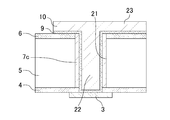
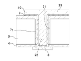
- the silicon device wafer 5 includes a first surface (device side surface) where an impurity region (not shown) of an active element such as a transistor or a diode is formed, and a side opposite to the first surface. It has the 2nd surface (back surface) which is a surface.
- a first insulating film (surface protective film) 4 is formed on the first surface of the silicon device wafer 5, and a metal film 3 serving as a wiring or a pad is formed on the first insulating film 4.
- the metal film 3 may be formed inside the first insulating film 4, but for the sake of simplicity, the metal film 3 is formed on the surface of the first insulating film 4.
- a state in which the metal film 3 is formed is illustrated.
- a second insulating film (back surface protective film) 6 is formed on the second surface of the silicon device wafer 5.
- a through via 22 is formed so as to penetrate from the first surface to the second surface of the silicon device wafer 5.
- the through via 22 is formed by sequentially filling the via hole 21 with the barrier metal film 9 and the conductive film 10.
- An insulating via coating film 7 c is formed between the sidewall of the through via 22 and the silicon device wafer 5.
- the via hole 21 is formed so as to penetrate the second insulating film 6 and the silicon device wafer 5, and the via coating film 7 c is formed on the inner wall of the via hole 21 in a portion located in the silicon device wafer 5.
- the sidewall 8b is formed on the inner wall of the portion of the via hole 21 located in the second insulating film 6 so as to be in contact with the via coating film 7c.
- connection portion for establishing electrical connection with the element on the device side surface of the silicon device wafer 5 through the through via 22. It has become.
- the through via 22 is formed so as to penetrate the first insulating film 4 in order to connect to the metal film 3 on the device side surface of the silicon device wafer 5.
- the barrier metal film 9 and the conductive film 10 constituting the through via 22 are formed by the second insulating film 6, the via coating film 7c, and the sidewall 8b, and silicon. Contact with the device wafer 5 can be prevented. Moreover, since the via coating film 7c having a low dielectric constant can be formed between the silicon device wafer 5 and the through via 22, the parasitic capacitance caused by the through via 22 can be reduced.
- an insulating polymer or an insulating film such as an MSQ film is used as the via coating film 7c (third insulating film 7a) formed on the sidewall of the through via 22. It may be used. Further, as the insulating polymer, it is preferable to use a material having a low dielectric constant and elastic modulus and good embedding characteristics. For example, a fluorinated polymer, a hydrocarbon-based polymer, or BCB (benzocyclobutene) is used. It is preferable to use a coating material or the like.
- the sidewall 8b (fourth insulating film 8a) formed on the inner wall of the via hole 21 in the portion located in the second insulating film 6 is a via coating film. It is preferable to use an insulating film that is less likely to be etched than the third insulating film 7a to be 7c. Specifically, when an insulating polymer is used as the via coating film 7c (third insulating film 7a), the fourth insulating film 8a is an insulating film having a high etching selectivity with respect to the insulating polymer, for example, CVD. It is preferable to use a silicon nitride film, a silicon carbide film, a silicon oxide film, or the like formed by the above method.
- a copper film or a conductive film made of, for example, tungsten or gold may be used as the conductive film 10 constituting the through via 22.
- a silicon nitride film or, for example, a silicon carbide film may be used as the second insulating film 6 formed on the back surface of the silicon device wafer 5.
- the silicon nitride film or the silicon carbide film is used in this way, the etching selectivity with respect to the insulating polymer can be increased, and the amount of abrasion of the second insulating film 6 can be reduced.
- FIGS. 3 (a) to 3 (h) A method for manufacturing a semiconductor device according to a first modification of the first embodiment of the present invention will be described below with reference to FIGS. 3 (a) to 3 (h).
- the materials, numerical values, and the like used in the present modification are examples, and the present invention is not limited to them.
- the present modification can be appropriately changed without departing from the scope of the technical idea of the present invention, and a combination of the present modification with other embodiments and modifications is also possible.
- the steps shown in FIGS. 3A, 3B, 3G, and 3H of the present modification are respectively the same as those in the first embodiment shown in FIGS. b), since it is the same as the process shown in FIG. 1G and FIG.
- the portion of the third insulating film 7a located above the surface of the second insulating film 6 is removed, and a dummy plug 7b made of the third insulating film 7a is formed.
- a resist film 31 having a thickness of, for example, about 1 ⁇ m is formed on the dummy plug 7 b and the second insulating film 6.
- the resist film 31 is patterned by lithography to form a resist pattern 31A that covers the second insulating film 6 and the via coating film formation region.
- the dummy plug 7b and the first insulating film 4 are etched using the resist pattern 31 as a mask to expose the metal film 3 at the bottom of the via hole 21.
- the resist pattern 31 is removed.
- a via coating film 7 c made of the remaining portion of the dummy plug 7 b (third insulating film 7 a) is formed on the inner wall of the via hole 21.
- the end on the back surface side of the silicon device wafer 5 in the via coating film 7 c is located in substantially the same plane as the surface of the second insulating film 6.
- FIGS. 3 (g) and 3 (h) are performed in the same manner as the steps shown in FIGS. 1 (g) and 1 (h) of the first embodiment.
- the via coating film 7c made of an insulating polymer using the sidewall 8b as a mask instead of forming the via coating film 7c made of an insulating polymer using the sidewall 8b as a mask as in the present modification described above, the via made of an insulating polymer using the resist pattern 31A as a mask. It is also possible to form the coating film 7c. Also in this modified example, since the third insulating film 7a serving as the via coating film 7c is embedded in the entire via hole 21 having a lower aspect ratio than that of the ring-shaped groove of the conventional example, the aspect ratio is low (that is, the opening is open). Therefore, the buried margin is increased and the through via 22 can be easily miniaturized.
- the semiconductor device according to this modification shown in FIG. 4 is different from the first embodiment shown in FIG. 2 in that the second insulating film (back surface protective film) on the second surface (back surface) of the silicon device wafer 5 is different. )
- the side wall of the through via 22 in the portion formed in 6 is covered with the via coating film 7c. Since the uppermost portion of the through via 22 is covered with the via coating film 7c made of an insulating polymer having a low dielectric constant, the capacitance between the upper corner of the through via 22 and the silicon device wafer 5 is reduced. Therefore, it is advantageous for speeding up.
- the yield deterioration due to peeling at the interface or the silicon device wafer 5 through the interface can be reduced. Since the occurrence of leakage current can be prevented, reliability is improved.
- FIGS. 5 (a) to 5 (h) a method for manufacturing a semiconductor device according to a second modification of the first embodiment of the present invention will be described with reference to FIGS. 5 (a) to 5 (h).
- the materials, numerical values, and the like used in the present modification are examples, and the present invention is not limited to them.
- the present modification can be appropriately changed without departing from the scope of the technical idea of the present invention, and a combination of the present modification with other embodiments and modifications is also possible.
- the steps shown in FIGS. 5A, 5B and 5D to 5H of this modification example are the same as those of FIG. 3A of the first modification example of the first embodiment, respectively. ), And steps similar to those shown in FIGS. 3B and 3D to 3H are omitted.
- FIGS. 5A and 5B first, similarly to the steps shown in FIGS. 3A and 3B of the first modification example of the first embodiment, FIGS. 5A and 5B. The process shown in FIG.
- the portion of the third insulating film 7a located above the surface of the second insulating film 6 is thinned to form a dummy plug 7b made of the third insulating film 7a.
- the third insulating film 7 a constituting the dummy plug 7 b remains on the surface of the second insulating film 6.
- FIGS. 5 (d) to 5 (h) are performed in the same manner as the steps shown in FIGS. 3 (d) to 3 (h) of the first modification of the first embodiment.
- a via coating film 7 c made of the remaining portion of the dummy plug 7 b (third insulating film 7 a) is formed on the inner wall of the via hole 21 and on the surface of the second insulating film 6.
- the via coating film 7 c can also be left on the surface of the second insulating film 6 formed on the back surface of the silicon device wafer 5. Also in this modified example, since the third insulating film 7a serving as the via coating film 7c is embedded in the entire via hole 21 having a lower aspect ratio than that of the ring-shaped groove of the conventional example, the aspect ratio is low (that is, the opening is open). Therefore, the buried margin is increased and the through via 22 can be easily miniaturized.
- the semiconductor device according to this modification shown in FIG. 6 is different from the first embodiment shown in FIG. 2 in that the second insulating film 6 formed on the back surface (second surface) of the silicon device wafer 5.
- the via coating film 7c is also formed on the surface.
- the second insulating film 6 and the via coating film 7c (third insulating film 7a) are laminated on the second surface of the silicon device wafer 5 is obtained, the second surface of the silicon device wafer 5 is obtained. Insulating properties can be improved.
- the via coating film 7c made of an insulating polymer having a low dielectric constant, the capacitance between the upper corner of the through via 22 and the silicon device wafer 5 is reduced. This is advantageous for speeding up. Further, as compared with the first embodiment, since there is no interface between the via coating film 7c and the sidewall 8b, the yield deterioration due to peeling at the interface or the silicon device wafer 5 through the interface can be reduced. Since the occurrence of leakage current can be prevented, reliability is improved.
- FIGS. 7 (a) to 7 (g) a method for fabricating a semiconductor device according to a third modification of the first embodiment of the present invention will be described with reference to FIGS. 7 (a) to 7 (g).
- the materials, numerical values, and the like used in the present modification are examples, and the present invention is not limited to them.
- the present modification can be appropriately changed without departing from the scope of the technical idea of the present invention, and a combination of the present modification with other embodiments and modifications is also possible.
- the steps shown in FIGS. 7B to 7G of this modification are the same as the steps shown in FIGS. 5C to 5H of the second modification of the first embodiment, respectively. Therefore, explanation is omitted.
- the silicon device wafer 5 is placed on the back side with the device side surface facing down. Is polished to a thickness of about 50 ⁇ m, for example.
- a first insulating film (surface protective film) 4 is formed on the device side surface of the silicon device wafer 5, and a metal film serving as a wiring or a pad is formed on the surface of the first insulating film 4. 3 is formed.
- the metal film 3 may be formed inside the first insulating film 4, but for the sake of simplicity, the metal film 3 is formed on the surface of the first insulating film 4. A state in which the film 3 is formed is illustrated.
- the glass carrier 1 is a tool for handling the silicon device wafer 5.
- a via hole 21 having a via diameter of 10 ⁇ m, for example, penetrating the silicon device wafer 5 is formed so as to reach the first insulating film 4.
- a via coating film 7 c composed of the remaining portion of the dummy plug 7 b (third insulating film 7 a) is formed on the inner wall of the via hole 21 and on the back surface of the silicon device wafer 5.
- the via coating film 7c ( A third insulating film 7a) can be formed on the back surface of the silicon device wafer 5. Also in this modified example, since the third insulating film 7a serving as the via coating film 7c is embedded in the entire via hole 21 having a lower aspect ratio than that of the ring-shaped groove of the conventional example, the aspect ratio is low (that is, the opening is open). Therefore, the buried margin is increased and the through via 22 can be easily miniaturized.
- the semiconductor device according to this modification shown in FIG. 8 is different from the first embodiment shown in FIG. 2 in that the second insulating film 6 is formed on the back surface (second surface) of the silicon device wafer 5.
- the via coating film 7 c is also formed on the second surface of the silicon device wafer 5.
- the via coating film 7c made of an insulating polymer having a low dielectric constant, the capacitance between the upper corner of the through via 22 and the silicon device wafer 5 is reduced.
- the yield deterioration due to peeling at the interface or the silicon device wafer 5 through the interface can be reduced. Since the occurrence of leakage current can be prevented, reliability is improved.
- the second insulating film 6 since the second insulating film 6 is not formed, the depth of the via hole 21 that embeds the through via 22 can be reduced, which is advantageous for embedding and the like. Thus, further miniaturization can be achieved.
- FIG. 9 shows a cross-sectional structure of a structure (laminated semiconductor device) according to the second embodiment of the present invention.
- an impurity region 53 of an active element such as a transistor or a diode is formed on the surface portion of the semiconductor substrate 51 on the first surface 52a side.
- a gate electrode 55 is formed on the first surface 52 a of the semiconductor substrate 51 via a gate insulating film 54.
- Each active element is electrically insulated by an element isolation 56 formed on the surface portion of the semiconductor substrate 51 on the first surface 52a side.
- a first interlayer insulating film 60a is formed on the first surface 52a of the semiconductor substrate 51 so as to cover the gate electrode 55, and is connected to the impurity region 53 and the gate electrode 55 in the first interlayer insulating film 60a.
- a contact 57 is formed.
- a second interlayer insulating film 60b and a third interlayer insulating film 60c are sequentially stacked on the first interlayer insulating film 60a.
- a first wiring 58a that is connected to the contact 57 and transmits a signal and supplies a power supply voltage in the semiconductor device, and a first via 59a that is connected to the first wiring 58a are formed.
- the third interlayer insulating film 60c there are a second wiring 58b that is connected to the first via 59a and transmits a signal and supplies a power supply voltage in the semiconductor device, and a second via 59b that is connected to the second wiring 58b. Is formed.
- an electrode pad 61 for connecting to the second via 59b and taking out a signal to the outside is formed.
- a through via 64 is formed so as to penetrate the semiconductor substrate 51 from the first surface 52a to the second surface 52b.
- the through via 64 is formed so as to also penetrate the first interlayer insulating film 60a on the first surface 52a side and the insulating protective film 65 on the second surface 52b side.
- the side wall of the through via 64 is covered with the via coating film 63 of the present invention. That is, the through via formation region A in FIG. 9 has the structure of the first embodiment shown in FIG. 2, FIG. 4, FIG. 6, or FIG. 2, 4, 6, and 8, the first surface 52 a side in the through via formation region A in FIG. 9 is shown on the lower side, and the second surface 52 b side is shown on the upper side.
- a plurality of semiconductor devices formed as described above are bonded to each other with the adhesive layer 62, and the semiconductor devices are electrically connected to each other through the through via 64, whereby a stacked structure is formed.
- the same via coating film 63 as that on the side wall of the through via 64 is formed.
- different insulating films are formed on the side wall of the portion of the through via 64 located in the first interlayer insulating film 60a and on the side wall of the portion of the through via 64 located in the semiconductor substrate 51, respectively. It may be formed as a via coating film.
- a plurality of semiconductor devices are stacked using the through via shown in the first embodiment. It becomes possible.
- the device can be reduced in size.
- the stacked structure shown in FIG. 9 the structure in which two semiconductor devices are stacked has been described as an example.
- two or more semiconductor devices can be stacked as appropriate. It is.
- 71A, 71B, and 71C are semiconductor substrates
- 72A, 72B, and 72C are insulating films that serve as via coating films
- 73A, 73B, and 73C are electrode pads
- 74A and 74B are through vias
- 75A, 75B, and 75C are wiring lines
- 76A, 76B, and 76C are bumps
- 77 is a semiconductor chip
- 78 is a bump
- 79 is a sealing resin.
- the through via formation region A in FIG. 10 has the structure of the first embodiment shown in FIG. 2, FIG. 4, FIG. 6, or FIG.
- a structure in which two or more semiconductor chips each having a logic circuit are stacked that is, a structure in which a plurality of semiconductor chips of the same type are stacked is shown.
- a structure in which a semiconductor chip having a logic circuit, a semiconductor chip having a memory element, a semiconductor chip having an imaging element, and a semiconductor chip having a MEMS (micro-electro-mechanical-systems) element are stacked that is, it is possible to form a structure in which a plurality of different types of semiconductor chips are stacked.
- An example of such a structure is shown in FIG. 10 to be a laminated structure shown in FIG.
- 71A, 71B, 71C, and 71D are semiconductor substrates
- 72A, 72B, 72C, and 72D are insulating films that serve as via coating films
- 73A, 73B, 73C, and 73D are Electrode pads
- 74A, 74B, 74C, and 74D are through vias
- 75A, 75B, 75C, and 75D are wiring lines
- 76A, 76B, 76C, and 76D are bumps
- 77 is a semiconductor chip
- 78 is a bump
- 79 is a sealing resin
- 82 is a semiconductor chip having a memory element
- 83 is a semiconductor chip having an imaging element.
- the through via formation region A in FIG. 11 has the structure of the first embodiment shown in FIG. 2, FIG. 4, FIG. 6, or FIG.
- the stacked structure shown in FIG. 9 (a structure in which the same kind of semiconductor chips are stacked or a structure in which different types of semiconductor chips are stacked) It is also possible to surface-mount on a printed wiring board 91 having a wiring structure 92.
- a laminated structure as shown in FIGS. 10 and 11 can be surface-mounted on a printed wiring board.
- a through-via is formed by forming a via hole from the back surface (opposite surface of the device-side surface) of the semiconductor substrate.
- a method of forming (or semiconductor chips) one by one has been described. However, instead of this, it is also possible to form a through via by forming a via hole from the surface (device side surface) side of the semiconductor substrate with another semiconductor substrate overlaid on the semiconductor chip, for example. is there.
- the metal film 3 shown in FIG. 1 (a), FIG. 3 (a), FIG. 5 (a) or FIG. 7 (a) is regarded as a pad of a semiconductor device located below, not shown.
- One insulating film 4 may be regarded as an adhesive layer.
Landscapes
- Internal Circuitry In Semiconductor Integrated Circuit Devices (AREA)
Priority Applications (1)
| Application Number | Priority Date | Filing Date | Title |
|---|---|---|---|
| US13/214,759 US8378462B2 (en) | 2009-03-04 | 2011-08-22 | Semiconductor device having through substrate vias |
Applications Claiming Priority (2)
| Application Number | Priority Date | Filing Date | Title |
|---|---|---|---|
| JP2009050758A JP5330863B2 (ja) | 2009-03-04 | 2009-03-04 | 半導体装置の製造方法 |
| JP2009-050758 | 2009-03-04 |
Related Child Applications (1)
| Application Number | Title | Priority Date | Filing Date |
|---|---|---|---|
| US13/214,759 Continuation US8378462B2 (en) | 2009-03-04 | 2011-08-22 | Semiconductor device having through substrate vias |
Publications (1)
| Publication Number | Publication Date |
|---|---|
| WO2010100705A1 true WO2010100705A1 (ja) | 2010-09-10 |
Family
ID=42709283
Family Applications (1)
| Application Number | Title | Priority Date | Filing Date |
|---|---|---|---|
| PCT/JP2009/007346 Ceased WO2010100705A1 (ja) | 2009-03-04 | 2009-12-28 | 半導体装置及びその製造方法 |
Country Status (3)
| Country | Link |
|---|---|
| US (1) | US8378462B2 (enExample) |
| JP (1) | JP5330863B2 (enExample) |
| WO (1) | WO2010100705A1 (enExample) |
Cited By (3)
| Publication number | Priority date | Publication date | Assignee | Title |
|---|---|---|---|---|
| US20120018895A1 (en) * | 2010-07-23 | 2012-01-26 | Tessera Research Llc | Active chip on carrier or laminated chip having microelectronic element embedded therein |
| US11329077B2 (en) | 2017-03-31 | 2022-05-10 | Sony Semiconductor Solutions Corporation | Semiconductor device with a through electrode reception part wider than a through electrode, solid-state imaging device, and electronic equipment |
| WO2023166843A1 (ja) * | 2022-03-01 | 2023-09-07 | ソニーセミコンダクタソリューションズ株式会社 | 半導体装置及び電子機器 |
Families Citing this family (29)
| Publication number | Priority date | Publication date | Assignee | Title |
|---|---|---|---|---|
| US7626269B2 (en) * | 2006-07-06 | 2009-12-01 | Micron Technology, Inc. | Semiconductor constructions and assemblies, and electronic systems |
| US8569876B2 (en) | 2006-11-22 | 2013-10-29 | Tessera, Inc. | Packaged semiconductor chips with array |
| US9640437B2 (en) | 2010-07-23 | 2017-05-02 | Tessera, Inc. | Methods of forming semiconductor elements using micro-abrasive particle stream |
| US8847380B2 (en) | 2010-09-17 | 2014-09-30 | Tessera, Inc. | Staged via formation from both sides of chip |
| US8736066B2 (en) | 2010-12-02 | 2014-05-27 | Tessera, Inc. | Stacked microelectronic assemby with TSVS formed in stages and carrier above chip |
| US8587126B2 (en) * | 2010-12-02 | 2013-11-19 | Tessera, Inc. | Stacked microelectronic assembly with TSVs formed in stages with plural active chips |
| CN102754102B (zh) * | 2010-12-09 | 2016-02-03 | 松下电器产业株式会社 | 三维集成电路的设计支持装置及设计支持方法 |
| US8742564B2 (en) * | 2011-01-17 | 2014-06-03 | Bai-Yao Lou | Chip package and method for forming the same |
| JP5958732B2 (ja) | 2011-03-11 | 2016-08-02 | ソニー株式会社 | 半導体装置、製造方法、および電子機器 |
| JP2012195514A (ja) | 2011-03-17 | 2012-10-11 | Seiko Epson Corp | 素子付き基板、赤外線センサー、および貫通電極形成方法 |
| WO2012142592A1 (en) * | 2011-04-14 | 2012-10-18 | Georgia Tech Research Corporation | Through package via structures in panel-based silicon substrates and methods of making the same |
| KR101828490B1 (ko) | 2011-08-30 | 2018-02-12 | 삼성전자주식회사 | 관통전극을 갖는 반도체 소자 및 그 제조방법 |
| US20130134600A1 (en) * | 2011-11-28 | 2013-05-30 | Advanced Semiconductor Engineering, Inc. | Semiconductor device and method for manufacturing the same |
| CN103219302B (zh) * | 2012-01-19 | 2016-01-20 | 欣兴电子股份有限公司 | 穿孔中介板 |
| KR101845529B1 (ko) | 2012-02-02 | 2018-04-05 | 삼성전자주식회사 | 관통전극을 갖는 반도체 소자 및 그 제조방법 |
| US10020244B2 (en) * | 2012-03-27 | 2018-07-10 | Cree, Inc. | Polymer via plugs with high thermal integrity |
| US8629524B2 (en) * | 2012-04-27 | 2014-01-14 | Taiwan Semiconductor Manufacturing Company, Ltd. | Apparatus for vertically integrated backside illuminated image sensors |
| KR101934864B1 (ko) * | 2012-05-30 | 2019-03-18 | 삼성전자주식회사 | 관통 실리콘 비아 구조물 및 그 제조 방법, 이를 포함하는 이미지 센서 및 그 제조 방법 |
| US9257384B2 (en) * | 2012-06-05 | 2016-02-09 | Stats Chippac Ltd. | Integrated circuit packaging system with substrate and method of manufacture thereof |
| KR101932660B1 (ko) | 2012-09-12 | 2018-12-26 | 삼성전자 주식회사 | Tsv 구조를 구비한 집적회로 소자 및 그 제조 방법 |
| JP2014107304A (ja) | 2012-11-22 | 2014-06-09 | Renesas Electronics Corp | 半導体装置およびその製造方法 |
| KR102299781B1 (ko) | 2014-07-21 | 2021-09-08 | 삼성전자주식회사 | 반도체 장치 및 이의 제조 방법 |
| CN104201115A (zh) * | 2014-09-12 | 2014-12-10 | 苏州晶方半导体科技股份有限公司 | 晶圆级指纹识别芯片封装结构及封装方法 |
| US9633930B2 (en) * | 2014-11-26 | 2017-04-25 | Kookmin University Industry Academy Cooperation Foundation | Method of forming through-hole in silicon substrate, method of forming electrical connection element penetrating silicon substrate and semiconductor device manufactured thereby |
| WO2019130702A1 (ja) * | 2017-12-27 | 2019-07-04 | ソニーセミコンダクタソリューションズ株式会社 | 撮像装置 |
| JP6994257B2 (ja) * | 2018-10-31 | 2022-02-21 | 国立大学法人茨城大学 | 配線構造 |
| JP7193731B2 (ja) * | 2019-03-29 | 2022-12-21 | 東京エレクトロン株式会社 | エッチング方法及びエッチング装置 |
| US11031348B2 (en) * | 2019-07-24 | 2021-06-08 | Nanya Technology Corporation | Semiconductor structure |
| CN111081632A (zh) * | 2019-12-12 | 2020-04-28 | 联合微电子中心有限责任公司 | 一种减小热应力的硅通孔结构及其制造方法 |
Citations (4)
| Publication number | Priority date | Publication date | Assignee | Title |
|---|---|---|---|---|
| JPH09205144A (ja) * | 1996-01-25 | 1997-08-05 | Sony Corp | 多層配線構造を有する半導体装置及びその製造方法 |
| JP2006060067A (ja) * | 2004-08-20 | 2006-03-02 | Rohm Co Ltd | 半導体チップの製造方法、半導体チップ、半導体装置の製造法および半導体装置 |
| JP2007281289A (ja) * | 2006-04-10 | 2007-10-25 | Fujikura Ltd | 電子部品及びその製造方法 |
| JP2008300718A (ja) * | 2007-06-01 | 2008-12-11 | Toshiba Corp | 半導体装置および半導体装置の製造方法 |
Family Cites Families (22)
| Publication number | Priority date | Publication date | Assignee | Title |
|---|---|---|---|---|
| US5493096A (en) * | 1994-05-10 | 1996-02-20 | Grumman Aerospace Corporation | Thin substrate micro-via interconnect |
| JP2570617B2 (ja) * | 1994-05-13 | 1997-01-08 | 日本電気株式会社 | 多層配線セラミック基板のビア構造及びその製造方法 |
| JPH09184080A (ja) * | 1995-12-27 | 1997-07-15 | Vacuum Metallurgical Co Ltd | 超微粒子による薄膜形成方法、およびその薄膜形成装置 |
| JP2000195861A (ja) * | 1998-12-25 | 2000-07-14 | Texas Instr Japan Ltd | 半導体装置およびその製造方法 |
| JP2002094082A (ja) * | 2000-07-11 | 2002-03-29 | Seiko Epson Corp | 光素子及びその製造方法並びに電子機器 |
| JP4053257B2 (ja) * | 2001-06-14 | 2008-02-27 | 新光電気工業株式会社 | 半導体装置の製造方法 |
| JP2003289073A (ja) * | 2002-01-22 | 2003-10-10 | Canon Inc | 半導体装置および半導体装置の製造方法 |
| US6826830B2 (en) * | 2002-02-05 | 2004-12-07 | International Business Machines Corporation | Multi-layered interconnect structure using liquid crystalline polymer dielectric |
| US6790775B2 (en) * | 2002-10-31 | 2004-09-14 | Hewlett-Packard Development Company, L.P. | Method of forming a through-substrate interconnect |
| JP4072677B2 (ja) * | 2003-01-15 | 2008-04-09 | セイコーエプソン株式会社 | 半導体チップ、半導体ウエハ、半導体装置及びその製造方法、回路基板並びに電子機器 |
| US6937120B2 (en) * | 2003-04-02 | 2005-08-30 | Harris Corporation | Conductor-within-a-via microwave launch |
| KR100651414B1 (ko) * | 2004-02-13 | 2006-11-29 | 삼성전기주식회사 | 동축 비아홀을 구비한 인쇄회로기판 |
| JP4955935B2 (ja) * | 2004-05-25 | 2012-06-20 | キヤノン株式会社 | 貫通孔形成方法および半導体装置の製造方法 |
| US7491582B2 (en) * | 2004-08-31 | 2009-02-17 | Seiko Epson Corporation | Method for manufacturing semiconductor device and semiconductor device |
| US7300857B2 (en) * | 2004-09-02 | 2007-11-27 | Micron Technology, Inc. | Through-wafer interconnects for photoimager and memory wafers |
| JP2006253631A (ja) | 2005-02-14 | 2006-09-21 | Fujitsu Ltd | 半導体装置及びその製造方法、キャパシタ構造体及びその製造方法 |
| US7629541B2 (en) * | 2006-06-19 | 2009-12-08 | Endicott Interconnect Technologies, Inc. | High speed interposer |
| JP2007005838A (ja) | 2006-10-12 | 2007-01-11 | Fujitsu Ltd | 半導体装置の支持体 |
| US20080136038A1 (en) * | 2006-12-06 | 2008-06-12 | Sergey Savastiouk | Integrated circuits with conductive features in through holes passing through other conductive features and through a semiconductor substrate |
| US7863180B2 (en) * | 2008-05-06 | 2011-01-04 | International Business Machines Corporation | Through substrate via including variable sidewall profile |
| US7973416B2 (en) * | 2008-05-12 | 2011-07-05 | Texas Instruments Incorporated | Thru silicon enabled die stacking scheme |
| US7968460B2 (en) * | 2008-06-19 | 2011-06-28 | Micron Technology, Inc. | Semiconductor with through-substrate interconnect |
-
2009
- 2009-03-04 JP JP2009050758A patent/JP5330863B2/ja active Active
- 2009-12-28 WO PCT/JP2009/007346 patent/WO2010100705A1/ja not_active Ceased
-
2011
- 2011-08-22 US US13/214,759 patent/US8378462B2/en active Active
Patent Citations (4)
| Publication number | Priority date | Publication date | Assignee | Title |
|---|---|---|---|---|
| JPH09205144A (ja) * | 1996-01-25 | 1997-08-05 | Sony Corp | 多層配線構造を有する半導体装置及びその製造方法 |
| JP2006060067A (ja) * | 2004-08-20 | 2006-03-02 | Rohm Co Ltd | 半導体チップの製造方法、半導体チップ、半導体装置の製造法および半導体装置 |
| JP2007281289A (ja) * | 2006-04-10 | 2007-10-25 | Fujikura Ltd | 電子部品及びその製造方法 |
| JP2008300718A (ja) * | 2007-06-01 | 2008-12-11 | Toshiba Corp | 半導体装置および半導体装置の製造方法 |
Cited By (7)
| Publication number | Priority date | Publication date | Assignee | Title |
|---|---|---|---|---|
| US20120018895A1 (en) * | 2010-07-23 | 2012-01-26 | Tessera Research Llc | Active chip on carrier or laminated chip having microelectronic element embedded therein |
| US8598695B2 (en) * | 2010-07-23 | 2013-12-03 | Tessera, Inc. | Active chip on carrier or laminated chip having microelectronic element embedded therein |
| US9355959B2 (en) | 2010-07-23 | 2016-05-31 | Tessera, Inc. | Active chip on carrier or laminated chip having microelectronic element embedded therein |
| US9859220B2 (en) | 2010-07-23 | 2018-01-02 | Tessera, Inc. | Laminated chip having microelectronic element embedded therein |
| US10262947B2 (en) | 2010-07-23 | 2019-04-16 | Tessera, Inc. | Active chip on carrier or laminated chip having microelectronic element embedded therein |
| US11329077B2 (en) | 2017-03-31 | 2022-05-10 | Sony Semiconductor Solutions Corporation | Semiconductor device with a through electrode reception part wider than a through electrode, solid-state imaging device, and electronic equipment |
| WO2023166843A1 (ja) * | 2022-03-01 | 2023-09-07 | ソニーセミコンダクタソリューションズ株式会社 | 半導体装置及び電子機器 |
Also Published As
| Publication number | Publication date |
|---|---|
| US8378462B2 (en) | 2013-02-19 |
| US20110304057A1 (en) | 2011-12-15 |
| JP2010205990A (ja) | 2010-09-16 |
| JP5330863B2 (ja) | 2013-10-30 |
Similar Documents
| Publication | Publication Date | Title |
|---|---|---|
| JP5330863B2 (ja) | 半導体装置の製造方法 | |
| KR101867961B1 (ko) | 관통전극을 갖는 반도체 소자 및 그 제조방법 | |
| TWI602273B (zh) | 半導體裝置 | |
| US7790608B2 (en) | Buried via technology for three dimensional integrated circuits | |
| TWI629759B (zh) | 晶片封裝體及其製造方法 | |
| KR101191492B1 (ko) | 반도체 장치 및 그 제조 방법 | |
| US8426252B2 (en) | Wafer level package having a stress relief spacer and manufacturing method thereof | |
| CN214672598U (zh) | 三维半导体装置结构和三维半导体装置 | |
| CN101483162B (zh) | 半导体装置及其制造方法 | |
| CN101752336B (zh) | 半导体装置及其制造方法 | |
| CN101996953B (zh) | 芯片封装体及其制造方法 | |
| US20180315620A1 (en) | Semiconductor device and method for manufacturing the same | |
| TWI732269B (zh) | 用於改善接合性的墊結構及其形成方法 | |
| JP2010045371A (ja) | 導電性保護膜を有する貫通電極構造体及びその形成方法 | |
| KR101896517B1 (ko) | 관통전극을 갖는 반도체 소자 및 그 제조방법 | |
| JP2011258687A (ja) | 半導体装置およびその製造方法 | |
| TWI532144B (zh) | 半導體裝置與其形成方法及半導體元件 | |
| US20150054136A1 (en) | Method of providing a via hole and routing structure | |
| CN107039394B (zh) | 半导体结构及其制造方法 | |
| CN106653682A (zh) | 集成电路结构及其形成方法 | |
| CN108807197A (zh) | 具有侧壁金属化部的芯片封装 | |
| WO2011036819A1 (ja) | 半導体装置の製造方法 | |
| JP4851163B2 (ja) | 半導体装置の製造方法 | |
| JP4764710B2 (ja) | 半導体装置とその製造方法 | |
| JP5751131B2 (ja) | 半導体装置及びその製造方法 |
Legal Events
| Date | Code | Title | Description |
|---|---|---|---|
| 121 | Ep: the epo has been informed by wipo that ep was designated in this application |
Ref document number: 09841071 Country of ref document: EP Kind code of ref document: A1 |
|
| NENP | Non-entry into the national phase |
Ref country code: DE |
|
| 122 | Ep: pct application non-entry in european phase |
Ref document number: 09841071 Country of ref document: EP Kind code of ref document: A1 |