WO2010089963A1 - 回路基板構造体 - Google Patents
回路基板構造体 Download PDFInfo
- Publication number
- WO2010089963A1 WO2010089963A1 PCT/JP2010/000328 JP2010000328W WO2010089963A1 WO 2010089963 A1 WO2010089963 A1 WO 2010089963A1 JP 2010000328 W JP2010000328 W JP 2010000328W WO 2010089963 A1 WO2010089963 A1 WO 2010089963A1
- Authority
- WO
- WIPO (PCT)
- Prior art keywords
- circuit board
- electrode
- solder
- electrodes
- component
- Prior art date
- Legal status (The legal status is an assumption and is not a legal conclusion. Google has not performed a legal analysis and makes no representation as to the accuracy of the status listed.)
- Ceased
Links
Images






Classifications
-
- H—ELECTRICITY
- H05—ELECTRIC TECHNIQUES NOT OTHERWISE PROVIDED FOR
- H05K—PRINTED CIRCUITS; CASINGS OR CONSTRUCTIONAL DETAILS OF ELECTRIC APPARATUS; MANUFACTURE OF ASSEMBLAGES OF ELECTRICAL COMPONENTS
- H05K1/00—Printed circuits
- H05K1/02—Details
- H05K1/11—Printed elements for providing electric connections to or between printed circuits
- H05K1/111—Pads for surface mounting, e.g. lay-out
-
- H—ELECTRICITY
- H05—ELECTRIC TECHNIQUES NOT OTHERWISE PROVIDED FOR
- H05K—PRINTED CIRCUITS; CASINGS OR CONSTRUCTIONAL DETAILS OF ELECTRIC APPARATUS; MANUFACTURE OF ASSEMBLAGES OF ELECTRICAL COMPONENTS
- H05K3/00—Apparatus or processes for manufacturing printed circuits
- H05K3/30—Assembling printed circuits with electric components, e.g. with resistors
- H05K3/32—Assembling printed circuits with electric components, e.g. with resistors electrically connecting electric components or wires to printed circuits
- H05K3/34—Assembling printed circuits with electric components, e.g. with resistors electrically connecting electric components or wires to printed circuits by soldering
- H05K3/341—Surface mounted components
- H05K3/3431—Leadless components
- H05K3/3436—Leadless components having an array of bottom contacts, e.g. pad grid array or ball grid array components
-
- H—ELECTRICITY
- H05—ELECTRIC TECHNIQUES NOT OTHERWISE PROVIDED FOR
- H05K—PRINTED CIRCUITS; CASINGS OR CONSTRUCTIONAL DETAILS OF ELECTRIC APPARATUS; MANUFACTURE OF ASSEMBLAGES OF ELECTRICAL COMPONENTS
- H05K2201/00—Indexing scheme relating to printed circuits covered by H05K1/00
- H05K2201/09—Shape and layout
- H05K2201/09209—Shape and layout details of conductors
- H05K2201/09372—Pads and lands
- H05K2201/09381—Shape of non-curved single flat metallic pad, land or exposed part thereof; Shape of electrode of leadless component
-
- H—ELECTRICITY
- H05—ELECTRIC TECHNIQUES NOT OTHERWISE PROVIDED FOR
- H05K—PRINTED CIRCUITS; CASINGS OR CONSTRUCTIONAL DETAILS OF ELECTRIC APPARATUS; MANUFACTURE OF ASSEMBLAGES OF ELECTRICAL COMPONENTS
- H05K2201/00—Indexing scheme relating to printed circuits covered by H05K1/00
- H05K2201/09—Shape and layout
- H05K2201/09209—Shape and layout details of conductors
- H05K2201/09372—Pads and lands
- H05K2201/09418—Special orientation of pads, lands or terminals of component, e.g. radial or polygonal orientation
-
- H—ELECTRICITY
- H05—ELECTRIC TECHNIQUES NOT OTHERWISE PROVIDED FOR
- H05K—PRINTED CIRCUITS; CASINGS OR CONSTRUCTIONAL DETAILS OF ELECTRIC APPARATUS; MANUFACTURE OF ASSEMBLAGES OF ELECTRICAL COMPONENTS
- H05K2203/00—Indexing scheme relating to apparatus or processes for manufacturing printed circuits covered by H05K3/00
- H05K2203/11—Treatments characterised by their effect, e.g. heating, cooling, roughening
- H05K2203/1178—Means for venting or for letting gases escape
-
- Y—GENERAL TAGGING OF NEW TECHNOLOGICAL DEVELOPMENTS; GENERAL TAGGING OF CROSS-SECTIONAL TECHNOLOGIES SPANNING OVER SEVERAL SECTIONS OF THE IPC; TECHNICAL SUBJECTS COVERED BY FORMER USPC CROSS-REFERENCE ART COLLECTIONS [XRACs] AND DIGESTS
- Y02—TECHNOLOGIES OR APPLICATIONS FOR MITIGATION OR ADAPTATION AGAINST CLIMATE CHANGE
- Y02P—CLIMATE CHANGE MITIGATION TECHNOLOGIES IN THE PRODUCTION OR PROCESSING OF GOODS
- Y02P70/00—Climate change mitigation technologies in the production process for final industrial or consumer products
- Y02P70/50—Manufacturing or production processes characterised by the final manufactured product
Definitions
- the present invention relates to a technique for directly connecting an electronic component such as a land grid array and a circuit board by solder without using lead wires.
- Solder is widely used for the connection between the electronic component and the circuit board.
- Sn-37Pb unit: mass% that can be soldered at around 220 ° C. has been widely used.
- lead Pb has a large environmental load, the use of solder that does not use lead is required.
- Lead-free solder alloys are less toxic but generally have poor wettability.
- the present invention relates to a method for connecting an electronic component such as a land grid array (LGA) and a circuit board using lead-free solder without using a lead wire.
- LGA land grid array
- solder In addition to poor wettability, lead-free solder generates huge bubbles due to outgas from the flux in the solder paste during solder reflow, and these bubbles remain in the solder even after the solder solidifies. Bubbles in the solder significantly reduce the connection strength.
- Patent Document 1 discloses that ultrasonic vibration is applied through a circuit board, and the molten solder is indirectly shaken with high energy although it has a small amplitude.
- a method of discharging voids caused by flux-out gas at the solder connection portion in units of substrates or preventing non-contact between the molten solder bump and the molten solder paste is described.
- Patent Document 2 a part such as BGA (Ball Grid Array) or LGA (Land Grid Array) or the like is used while the solder is melted instead of vibrating through the circuit board.
- a method is described in which only the target part is connected to a vibrator with a clamp, and ultrasonic vibration is directly performed in parts.
- FIG. 1 is a diagram showing a state in which the land grid array 10 and the circuit board 1 are connected in a leadless manner.
- rectangular component electrodes 11 are formed in a matrix on the land grid array 10.
- circuit board electrodes 2 are formed in a matrix corresponding to the component electrodes 11 of the land grid array 10.
- a solder paste 20 is formed on the circuit board electrode 2 by printing or the like.
- the component electrode 11 may be referred to as a land grid array electrode
- the circuit board electrode 2 may be referred to as a board land.
- FIG. 1 (b) shows a state in which the land grid array 10 and the circuit board 1 are connected by solder.
- a surface mount component having a square electrode formed on the bottom surface of a package instead of having a lead, such as a land grid array 10 (Land Grid Array) is reflow soldered with the solder paste 20, the component electrode 11 and the substrate A huge bubble 100 due to outgas from the flux is generated from the solder paste 20 supplied to the narrow gap portion between the lands, and this remains in the solder even after the solder is solidified.
- FIG. 1C is an enlarged view of the solder connection portion in a state where the land grid array 10 and the circuit board 1 are connected. Solder melted by reflow is formed between the component electrode 11 and the circuit board electrode 2 in FIG. Bubbles 100 exist in the solder. As for the remaining bubbles 100, the average value of the upper 10% diameters is approximately 0.7 times the land size, which causes a problem of remarkably reducing the solder connection strength.
- the air bubbles 100 in the solder are preferably discharged to the outside when the solder is melted, but most of them remain inside.
- This bubble residue also depends on the shape of the side surface of the solder being melted during reflow.
- FIG. 2 shows an example in which bubbles 100 are generated in the vicinity of the molten solder surface 22.
- FIG. 2A shows a case where bubbles 100 are generated in the vicinity of the molten solder surface 22 when the molten solder surface 22 is planar.
- FIG. 2B shows an example in which the molten solder surface 22 has a convex shape toward the outside. As shown in FIG.
- solder paste 20 that generates less outgas.
- there are adverse effects such as deterioration of paste printability and solder wettability. There is.
- An object of the present invention is to realize a highly reliable leadless solder connection by reducing bubbles 100 contained in the solder in leadless solder connection. And in order to realize this, it is possible to discharge bubbles inside the solder without changing the reflow process conditions or modifying the process itself, changing the configuration, or using solder paste using special flux. It is.
- the board-side land is moved to a position rotated around its center as an axis, It reduces the surface energy of the molten solder during reflow soldering and promotes the discharge of bubbles.
- the second means is that when soldering the surface-mounted component, the board-side land is shifted from the position directly below the surface-mounted component electrode so that the sum of external forces acting on the surface-mounted component becomes zero while the solder is melted.
- the surface energy of the molten solder at the time of reflow soldering is reduced, and the discharge of bubbles is promoted.
- the third method is to reduce the surface energy of the molten solder during reflow soldering by soldering surface mount components by forming a smooth concave shape with at least one side of the land on the board side facing the outside. It promotes the discharge of bubbles.
- the fourth means is a combination of any of the first to third means.
- the present invention it is possible to discharge bubbles in the land grid array connection portion without using a reflow process condition or a solder paste using a special flux, so that it is possible to form a solder connection portion that is resistant to thermal fatigue. .
- This enables highly reliable leadless soldering.
- FIG. 3 is a plan view illustrating a relationship between a circuit board electrode and a component electrode in Example 1.
- FIG. 3 is a detailed view showing a relationship between a circuit board electrode and a component electrode in Example 1.
- FIG. 3 is a perspective view which shows the relationship between the circuit board electrode in Example 1, and a component electrode.
- It is sectional drawing which ties P1, P2, and P3 in FIG.
- It is a top view which shows the relationship between an electrode dimension and an electrode pitch.
- 6 is a plan view showing an arrangement of circuit board electrodes of Example 2.
- FIG. 3 is a plan view illustrating a relationship between a circuit board electrode and a component electrode in Example 1.
- FIG. 3 is a detailed view showing a relationship between a circuit board electrode and a component electrode in Example 1.
- It is a perspective view which shows the relationship between the circuit board electrode in Example 1, and a component electrode.
- It is sectional drawing which ties P1, P2, and P3 in FIG.
- It is a top view
- FIG. 6 is a plan view showing another arrangement of circuit board electrodes in Example 2.
- FIG. It is a schematic diagram which shows the direction of the force by the self-alignment of molten solder.
- 6 is a plan view showing an example of the shape of a circuit board electrode of Example 3.
- FIG. It is a top view which shows the relationship between the circuit board electrode of Example 4, and a component electrode.
- Each terminal group, output terminal group, and ground terminal group of electrodes on the circuit board side connecting the land grid array are formed by three metal foils that are only divided by the supply of solder resist. It is the perspective view which showed.
- FIG. 10 is a perspective view showing a relationship between a circuit board electrode and a component electrode in Example 5.
- FIG. 3 is a plan view showing the positional relationship between the component electrode 11 and the circuit board electrode 2.
- the circuit board electrode 2 (substrate side land) indicated by the solid line is rotated with respect to the component electrode 11 (land grid array side electrode) indicated by the dotted line.
- the surface area of the solder side surface is increased as compared with the case where the land is not rotated. Therefore, even if the solder supplied between the land grid array 10 side electrode and the substrate land melts, A part forms a flat surface or a concave surface toward the outside, and the bubble discharge property is improved from the side surface of the solder. That is, if the solder surface has a concave shape, a phenomenon opposite to that in the convex shape described with reference to FIG. 2 occurs, and the bubbles 100 are easily removed from the solder surface.
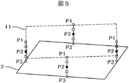
- FIG. 5 is a perspective view showing the positional relationship between the component electrode 11 and the circuit board electrode 2.
- the position of the component electrode 11 corresponding to the point P where the sides of the component electrode 11 and the circuit board electrode 2 in FIG. 4 intersect is P1
- the position corresponding to the circuit board electrode 2 is P3.
- the component electrode 11 and the circuit board electrode 2 are separated by the thickness of the solder.
- An intermediate position between P1 and P3 is P2.
- the mark of represents that the interval between P1 and P2 is the same as the interval between P3 and P2.
- the solder surface in the vicinity indicated by P1, P2, and P3 is likely to be concave, and a force directed to this location acts on the bubble 100. That is, the line connecting P1, P2, and P3 is concave toward the outside.
- This state is shown in FIG.
- the molten solder 21 has a convex shape with respect to the internal bubbles 100, the bubbles 100 break out of the solder surface and easily escape to the outside.
- the angle ⁇ for making the shape of the line connecting P1, P2, and P3 concave so as to allow the bubble 100 to escape to the outside is maximum at 45 degrees.
- the ratio of land pitch Q: land size S or the ratio of electrode pitch Q: electrode size S as shown in FIG. If it exceeds, bridge will begin to occur. Further, since the effect is reduced when the angle is approximately 15 ° or less, it is desirable that the angle ⁇ is 15 ° to 20 °.
- the example of the specific process in the present embodiment is as follows. That is, the component electrode pitch: 1.2 mm, the component electrode shape: square, the component electrode size: 0.7 mm, the number of component electrodes: 77, the land grid array 10 and the solder alloy composition: Sn-3Ag-0.5Cu solder paste 20 Reflow soldering was performed using a solder paste printing thickness of 0.15 mm.
- the printed circuit board used for soldering was prepared with a substrate base material: FR-4, a substrate thickness: 1.6 mm, and a land copper foil thickness: 18 ⁇ m.
- the land layout of the board is the same as that of the land grid array 10 in the land pitch, land shape, and land size, and the land periphery has four sides parallel to the land arrangement direction (conventional specification A) and the land of the board.
- a product (improved specification A) moved to a position rotated by 18 ° around the center was prepared.
- the average life in this embodiment is about 0.7L.
- the average life is 0.5 L, which is a significant improvement compared to this.
- the board-side land acts on the surface-mounted component during solder melting.
- the position is shifted from a position directly below the surface-mounted component electrode 11 so that the sum of the external forces becomes zero. By doing so, the surface energy of the molten solder 21 during reflow soldering is reduced, and the discharge of the bubbles 100 is promoted.
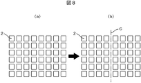
- FIG. 8 shows an example of this embodiment.
- FIG. 8A shows the arrangement of the circuit board electrodes 2 in the conventional circuit board 1.
- FIG. 8B shows the arrangement of the circuit board electrodes 2 on the circuit board 1 in this embodiment.
- the circuit board electrodes 2 are evenly arranged, but in FIG. 8 (b), the electrode spacing is large at the center line C, and the electrode spacing is on the right and left sides of the center line. This is the same as FIG.
- FIG. 7 shows an arrangement example of the circuit board land 2.
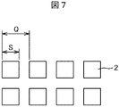
- the land pitch is Q and the land size is S.
- the effect starts to appear when the shift amount is approximately 1/8 or more of the land size.
- the bridge starts to appear when the shift amount is approximately one fifth of the land size or more, and when the shift amount is approximately one fourth or more of the land size, the solder grid is poorly spread to the electrodes of the land grid array 10 or the board land. In consideration of the fact that it starts to appear, it is desirable that the shift amount is 1/8 to 1/4 or less of the land size.
- the shifting direction of the board-side land in addition to shifting to a position shifted to both sides from the center line that bisects the surface mount component, as shown in FIG. In addition, it is possible to move to a position radially shifted from the center point of the surface mount component.
- the circuit board electrode 2 is shifted to the left and right across the center line, but the same effect can be obtained by shifting the circuit board 1 in the vertical direction across the center line. .
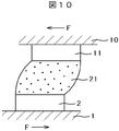
- FIG. 10 shows a state in which the circuit board electrode 2 and the component electrode 11 are solder-connected with the centers being shifted.
- F the solder is melted in such an arrangement, it is indicated by F between the circuit board electrode 2 and the component electrode 11 or between the circuit board 1 and the land grid array 10 due to the self-alignment effect by the molten solder 21. Power works.
- the component electrode pitch 1.2 mm
- the component electrode shape square
- the component electrode size 0.7 mm
- the number of component electrodes 88 (8 rows and 11 columns)
- the solder alloy composition Sn-3Ag-0.5 Reflow soldering was performed using a Cu solder paste 20 with a solder paste printing thickness of 0.15 mm.
- the printed circuit board used for soldering was prepared with a substrate base material: FR-4, a substrate thickness: 1.6 mm, and a land copper foil thickness: 18 ⁇ m.
- the land layout of the substrate is the same as that of the land grid array 10 in the land pitch, land shape, and land size, and the land of the four sides of the land is parallel to the land arrangement direction (conventional specification B). 44 (4 rows and 11 columns) pieces were divided in two, and each land was separated by 0.15 mm from the straight line to be divided (improved specification B).
- the substrate-side land is provided with a recess having a depth of 0.1 times or more the land size.
- the land size is L
- the amount of the recess is R. That is, R is greater than 0.1L.
- the depth of the dent is preferably about 0.1 to 0.2 times the land size.
- this dent is formed by a curve with a small radius of curvature or a broken line that bends at a steep angle, it becomes difficult for the solder to spread out following the shape. Therefore, the dent needs to be as smooth as possible.
- the smooth recess can be formed by smoothly connecting a single quadratic curve, an arc, or a plurality of these.
- the component electrode pitch 1.2 mm
- the component electrode shape square
- the component electrode size 0.7 mm
- the number of component electrodes 90 (9 rows and 10 columns)
- the solder alloy composition Sn-3Ag-0.5 Reflow soldering was performed using a Cu solder paste 20 with a solder paste printing thickness of 0.15 mm.
- the printed circuit board used for soldering was prepared with a substrate base material: FR-4, a substrate thickness: 1.6 mm, and a land copper foil thickness: 18 ⁇ m.
- the land layout of the substrate is the same as the land grid array 10 in the land pitch, land shape, and land size, and the four sides of the land outer periphery are parallel to the land arrangement direction (conventional specification C).
- the present embodiment is a combination of the first to third embodiments described above. As a result, it is possible to improve the effect as compared with the case where the first to third embodiments are carried out alone.
- FIG. 12 shows an example in which Example 1 and Example 3 are combined.
- FIG. 12A is a plan view showing a state in which the circuit board electrode 2 and the component electrode 11 are combined
- FIG. 12B is a partial detailed view of FIG. 12A.
- the circuit board electrode 2 is inclined by ⁇ degrees with respect to the component electrode 11 indicated by a dotted line. Further, a recess having a depth 0.1 times the land size L is provided on one side of the circuit board electrode 2.
- the effect of inclining the circuit board electrode 2 and the component electrode 11 and the effect of forming the recesses in the circuit board electrode 2 are combined, so that the molten solder surface 22 is formed more than in the case of the first or third embodiment. A large recess is formed. Therefore, the size of the remaining bubbles 100 can be further reduced.
- a dent is formed on both sides of the point P by a curve smoothly connecting two types of arcs having different radii of curvature. That is, in FIG. 12B, the curve 3 is a first arc, the curve 4 is a second arc, and the first arc and the second arc have different radii of curvature. However, a straight line passing through the center of the electrode and having an inclination ⁇ / 2 degrees intersects with the curve 3 and the curve 4 at one point. The depth Q at this time is 0.1L.
- the bubble 100 is naturally discharged from this recess, and the average value of the upper 10% diameter of the remaining bubble 100 is about 0.3 times the land size.
- the average life was about 0.8 L, where L was the life when no bubbles 100 existed.
- this proposal is not applied, there are huge voids remaining in many connection parts, and the average life is 0.5 L. Therefore, the reliability is greatly improved.
- the specific process of this example is as follows. Component electrode pitch: 1.2 mm, component electrode shape: square, component electrode size: 0.7 mm, number of component electrodes: 77, land grid array 10 and solder alloy composition: Sn-3Ag-0.5Cu solder paste 20 Reflow soldering was performed with a solder paste printing thickness of 0.15 mm.
- the printed circuit board used for soldering was prepared with a substrate base material: FR-4, a substrate thickness: 1.6 mm, and a land copper foil thickness: 18 ⁇ m.
- the land layout of the substrate is the same as the land grid array 10 in the land pitch, land shape, and land size, and the land of the substrate is moved to a position rotated about the center by 18 ° (improved specification A)
- a land an improved specification A ′
- a recess formed by smoothly connecting two kinds of arcs having a depth of 0.12 mm on one side of the land of the improved specification A was prepared.
- each substrate-side electrode is formed by being individually separated by etching, but the land grid array connected to the circuit board depends on the type. There is a need to increase the heat dissipation efficiency and to increase the adhesive strength between the substrate-side electrode and the substrate base material.
- At least two electrodes through which the same signal flows among the electrodes connected to each signal terminal among the electrodes on the circuit board side are one sheet that is only divided by the solder resist supply. It may be formed of metal foil.
- the land grid array is a component such as a DC-DC converter, a transistor array, or an assembly of passive components, and some of the electrodes are components that use the same signal. This is an effective means because the electrode can be formed from a single metal foil.
- the signal terminals on the land grid array side that use the same signal and the electrodes on the circuit board side that use the same signal are formed from a single large metal foil, they are used in the solder joints.
- the size of the void caused by the remaining flux-out gas increases in correlation with the size of the connecting portion. Further, there is a demerit that the closer the void generation position is to the vicinity of the central portion of the connection portion, the easier it is to remain in the connection portion, and the strength of the solder connection portion is reduced.
- this means makes it possible to increase the electrode area on the board side, and to transfer the amount of heat generated in the component to the board base material in a short time, thus improving heat dissipation. There is a merit that it becomes possible.
- FIG. 13 shows that each of the input terminal group, the output terminal group, and the ground terminal group of the electrodes on the side of the circuit board 1 to which the land grid array 10 is connected has three metal foils (circuit board electrodes 2). It is the figure which showed a mode that it was dividedly formed by the opening part 31 of the soldering resist 30 supplied to FIG.
- the present embodiment is an example in which the above concept is combined with the fourth embodiment. Thereby, compared with the case where Example 4 is implemented independently, it becomes possible to raise heat dissipation efficiency and to raise the adhesive strength effect of a board
- FIG. 14 is a diagram showing an example in which the above concept is combined with the fourth embodiment.
- FIG. 14 is formed by changing the shape of the opening 31 in the solder resist 30 supplied on the circuit board electrode in FIG.
- the shape of each of the input terminal, output terminal, and ground terminal of the electrode on the circuit board side, that is, the shape of the solder resist opening 31 is the same as that in FIG.
- the present embodiment is specifically as follows. That is, the component electrode pitch: 1.2 mm, the component electrode shape: square, the component electrode size: 0.7 mm, the number of component electrodes: 77, the land grid array 10 and the solder alloy composition: Sn-3Ag-0.5Cu solder paste 20 Reflow soldering was performed using a solder paste printing thickness of 0.15 mm.
- the printed circuit board used for soldering was prepared with a substrate base material: FR-4, a substrate thickness: 1.6 mm, and a land copper foil thickness: 18 ⁇ m.
- the land layout of the substrate is the same as the land grid array 10 in the land pitch, land shape, and land size, and the substrate land is moved to a position rotated about the center by 18 ° and 0.12 on one side of the substrate land.
- a recess formed by smoothly connecting two kinds of arcs with a depth of mm is provided, and the land shape is formed by separating copper foils by etching (as used in Example 4).
- the same improved specification A ′) was prepared.
- each of the input terminal group, the output terminal group, and the ground terminal group of the electrodes on the circuit board side connecting the land grid array is divided by solder resist supply.
- Each land was also prepared by making the shape of the portion where no solder resist was supplied the same as the improved specification A ′ (the improved specification A ′′).
- each of the terminal group, the output terminal group, and the ground terminal group is formed of a single metal foil that is divided only by the supply of solder resist, the heat generated in the components can be transferred to the board without impairing the connection reliability. The heat dissipation performance can be improved.
Landscapes
- Engineering & Computer Science (AREA)
- Microelectronics & Electronic Packaging (AREA)
- Manufacturing & Machinery (AREA)
- Electric Connection Of Electric Components To Printed Circuits (AREA)
- Structures For Mounting Electric Components On Printed Circuit Boards (AREA)
Abstract
回路基板とランドグリッドアレイ等の電子部品のリードレス接続における半田内 の気泡を減少させ、接続の信頼性を向上させることを目的とする。ランドグリッドアレイにおける部品電極11はマトリクス状に配置しており、回路基板における回路基板電極2もマトリクス状に配置している。点線で示す部品電極11に対し、回路基板電極2を角度θだけ傾ける。部品電極11の辺と回路基板電極2の辺と交わる点をP1としたとき、点P1における溶融半田の断面形状は外側に対して凹形状となるので、溶融半田内の大型気泡が抜けやすい構造となる。本発明によれば、半田内における大型気泡が減少するので、リードレス半田の信頼性を向上させることが出来る。
Description
本発明は、ランドグリッドアレイ等の電子部品と回路基板とをリード線を用いず、鉛を用いない半田によって直接接続する技術に関する。
電子部品と回路基板の接続には、半田が広く用いられているが、従来この半田には220℃付近で半田付けすることが出来るSn-37Pb(単位:質量%)が広く用いられてきた。しかし、鉛Pbは環境負荷が大きいので、鉛を用いない半田の使用が求められている。鉛フリー半田合金は毒性が少ないが、一般的にぬれ性が悪い。本発明は、鉛フリー半田を用いてランドグリッドアレイ(LGA(Land Grid Array))等の電子部品と回路基板とをリード線を用いずに接続する方法に関するものである。
鉛フリー半田では、濡れ性が悪いほかに、半田リフロー時に半田ペースト中のフラックスからのアウトガスに起因する巨大な気泡が発生し、この気泡は、半田が凝固した後も半田中に存在する。半田の中の気泡は接続強度を著しく減少させる。
半田中の気泡の存在を減少させるために、「特許文献1」には、回路基板を介して超音波振動を与え、間接的に溶融半田に微小振幅ではあるが高エネルギーで揺さぶりをかけることで、基板単位で半田接続部のフラックスアウトガス基因のボイド排出、あるいは溶融した半田バンプと溶融した半田ペーストの未接防止を行なう方法が記載されている。
また、「特許文献2」には、回路基板を介して加振するのではなく、半田が溶融している間に、BGA(Ball Grid Array)やLGA(Land Grid Array)等のような一部の対象部品だけをクランプ付きの振動子に接続して、部品単位で直接超音波加振する方法が記載されている。
図1はランドグリッドアレイ10と回路基板1をリードレス接続する様子を示す図である。図1(a)において、ランドグリッドアレイ10には矩形状の部品電極11がマトリクス状に形成されている。一方、回路基板1には、ランドグリッドアレイ10の部品電極11に対応して回路基板電極2がマトリクス状に形成されている。回路基板電極2には印刷等によって半田ペースト20が形成されている。以後、部品電極11のことをランドグリッドアレイ電極、回路基板電極2のことを基板ランドということもある。
図1(b)は、ランドグリッドアレイ10と回路基板1を半田によって接続した状態を示すものである。ランドグリッドアレイ10(Land Grid Array)などのリードを持たない代わりにパッケージの底面に正方形の電極が形成された表面実装部品を、半田ペースト20を用いてリフロー半田付けする際、部品電極11と基板ランド間の狭間隙部に供給された半田ペースト20からフラックスからのアウトガス起因の巨大な気泡100が発生し、これが半田凝固後も半田中に残留する。
図1(c)は、ランドグリッドアレイ10と回路基板1が接続された状態における半田接続部の拡大図である。図1(c)における部品電極11と回路基板電極2の間にはリフローによって溶融した半田が形成されている。半田内には気泡100が存在している。残留する気泡100については、その上位10%の直径の平均値がランドサイズの概ね0.7倍程度になることにより、半田接続強度を著しく低下させることが問題となっている。
半田内の気泡100は、半田が溶融している状態において、外部に排出されることが望ましいが、その多くは内部に残留してしまう。この気泡残留(排出のしにくさ)は、リフロー時に溶融中の半田の側面形状にもよる。図2は溶融半田表面22付近に気泡100が発生した場合の例を示すものである。図2(a)は、溶融半田表面22が平面状である場合に、溶融半田表面22付近に気泡100が発生した場合である。図2(b)は溶融半田表面22が外部に向けて凸形状をしている例である。図2(b)のように、溶融半田表面22が外部に向けて凸形状をしていると、半田表面にアウトガスの気泡100が接近したとき、半田表面と気泡100の間に存在する溶融半田21が薄皮状になる部分23が大きくなる。したがって、図2(b)のような形状では、気泡100が排出されにくい。
そして、鉛フリー半田は比較的表面張力が大きく、球状に凝集する性質が大きいため、薄皮状になるには大きな表面エネルギーが必要となる。従って、上記の場合、気泡100が半田表面に接近するだけで、溶融半田21の表面エネルギーは著しく増加してしまうため、気泡排出のための活性化エネルギー増加により、気泡100は容易に排出されない。
現状では、この問題解決のためには、アウトガス発生の少ない半田ペースト20を使用するしか方法がないが、ガスの発生量が減少する代わりに、ペーストの印刷性・半田のぬれ性悪化などの弊害がある。
本発明の課題は、リードレス半田接続において、半田内に含有される気泡100を減少させ、信頼性の高いリードレス半田接続を実現することである。そして、これを実現するために、リフロープロセスの条件あるいはプロセス自体の改造や構成の変更をしたり、特別なフラックスを使用した半田ペーストを使用することなく、半田内部の気泡排出を可能とすることである。
第一の手段は、ランドグリッドアレイなどのリードを持たない表面実装部品を半田付けする際、図3に示すように、基板側ランドをその中心を軸にして回転させた位置に移すことにより、リフロー半田付け時の溶融半田の表面エネルギーを低減させ、気泡の排出を促進するものである。
第二の手段は、表面実装部品を半田付けする際、基板側ランドを半田溶融中に該表面実装部品に働く外力の総和がゼロになるように、表面実装部品電極の直下の位置からずらした位置に移すことにより、リフロー半田付け時の溶融半田の表面エネルギーを低減させ、気泡の排出を促進するものである。
第三の手段は、表面実装部品を半田付けする際、基板側ランドの少なくともランドの一辺を外部に向けてなめらかな凹形状とすることにより、リフロー半田付け時の溶融半田の表面エネルギーを低減させ、気泡の排出を促進するものである。
第四の手段は、上記第1の手段乃至第3の手段をいずれかを組み合わせることである。
本発明により、リフロープロセス条件や特別なフラックスを使用した半田ペーストを使用することなく、ランドグリッドアレイ接続部内の気泡の排出が可能になるので、熱疲労に強い半田接続部の形成が可能となる。これによって信頼性の高いリードレス半田が可能になる。
以下、実施例を用いて本発明の内容を詳細に説明する。
本実施例では、回路基板電極2を部品電極11に対してその中心の軸を回転させる。この様子を図3に示す。図3は部品電極11と回路基板電極2の位置関係を示す平面図である。図3において、点線で示す部品電極11(ランドグリッドアレイ側電極)に対して実線で示す回路基板電極2(基板側ランド)を回転させている。
図3のような構成によって、ランドを回転させない場合と比較して、半田側面の表面積が増大するため、ランドグリッドアレイ10側電極と基板ランド間に供給された半田が溶融しても半田表面の一部は外部に向けて平面か凹面を形成し、半田の側面から気泡排出性が向上することになる。すなわち、半田表面が凹形状となれば、図2で説明した凸形状にある場合の反対の現象が起こり、半田表面から気泡100が抜けやすくなる。
図4を用いて本実施例をさらに詳細に説明する。いま、正方形の部品電極11(ランドグリッドアレイ10側電極)に対する正方形の回路基板電極2(基板側ランド)の回転角をθ°とした場合を考えることにする。このとき、部品電極11の辺と回路基板電極2の辺が交差する点と部品電極11あるいは回路基板電極2の中止とを結ぶ線は、θ/2傾いていることになる。
図5は、部品電極11と回路基板電極2の位置関係を示す斜視図である。図4における部品電極11と回路基板電極2の辺が交わる点Pに対応する部品電極11の位置がP1であり、回路基板電極2に対応する位置がP3である。部品電極11と回路基板電極2は半田の厚さだけ離れている。P1とP3の中間の位置がP2である。図5において、=のマークはP1とP2の間隔とP3とP2の間隔が同じであることを表している。
図5において、P1、P2、P3で示す付近の半田表面は凹面化しやすく、気泡100にはこの場所に向かう力が働くことになる。すなわち、P1、P2、P3を結ぶ線は外側に向かって凹形状となっている。この状態を図6に示す。図6に示すように、溶融半田21は内部の気泡100に対しては凸形状となっているので、この気泡100は、半田の表面を破壊して容易に外部に抜けていく。
図4および図5において、気泡100が外部に抜けるようにするためにP1、P2、P3を結ぶ線の形状を凹形状とするための角度θは45度で最大となる。しかし、図7に示すような、ランドピッチQ:ランドサイズSの比、あるいは電極ピッチQ:電極サイズSの比が5:3程度の一般的なランドグリッドアレイ実装の場合、θが概ね20°を超えると、ブリッジが発生しはじめる。また、 概ね15°以下では効果が減少するため、 θは15°乃至20°であることが望ましい。
本実施例における具体的なプロセスの例は次のとおりである。すなわち、部品電極ピッチ:1.2mm、部品電極形状:正方形、部品電極サイズ:0.7mm、部品電極数:77のランドグリッドアレイ10、および、半田合金組成:Sn-3Ag-0.5Cuの半田ペースト20を用いて、半田ペースト印刷厚:0.15mmとしてリフロー半田付けを実施した。
半田付けに使用したプリント基板は、基板基材:FR-4、基板厚:1.6mm、ランド銅箔厚:18μmのものを用意した。なお、基板のランド配置は、ランドピッチ、ランド形状、ランドサイズが、ランドグリッドアレイ10と同じで、ランド外周の4辺がランド配列方向に平行なもの(従来仕様A)と、基板のランドをその中心を軸にして18°回転させた位置に移したもの(改良仕様A)を用意した。
従来仕様を100個と改良仕様Aを100個、リフロー半田付け後、全ての半田接続部のX線透視観察を実施した。その結果、残留する気泡100について、その上位10%の直径の平均値は、従来仕様Aについては、0.45mmになったが、改良仕様Aについては、0.34mmになった。
また、-55~125℃、1サイクル/時の条件で温度サイクル試験を実施した。その結果、従来仕様Aにおいて、気泡100が全く存在しない場合の寿命が約1500サイクルではあるが、平均寿命は約800サイクルになった。一方、改良仕様Aの平均寿命は約1100サイクルになった。したがって、本案を適用した改良仕様Aの場合、その平均寿命が改善されていることがわかった。
本実施例の効果をまとめると次のようになる。すなわち、巨大な気泡100は図6におけるP2点付近より、自然に排出され、残留する気泡100については、その上位10%の直径の平均値がランドサイズの概ね0.5倍程度になる。
温度サイクル試験により、半田接続部に熱機械的ストレスを与える試験を実施すると、気泡100が全く存在しない場合の寿命をLとした場合、本実施例における平均寿命は0.7L程度になる。しかし、本実施例を適用しない場合、多くの接続部に巨大なボイドの残留があり、その平均寿命は0.5Lであるので、これと比較すると、大きく改善されていることになる。
第2に実施例は、基板側ランドをその中心を軸にして回転させた位置に移す代わりに、表面実装部品を半田付けする際、基板側ランドを、半田溶融中に該表面実装部品に働く外力の総和がゼロになるように、表面実装部品電極11の直下の位置からずらした位置に移すものである。こうすることによって、リフロー半田付け時の溶融半田21の表面エネルギーを低減させ、気泡100の排出を促進するものである。
図8に本実施例の1例を示す。図8(a)は従来の回路基板1における回路基板電極2の配置である。図8(b)は本実施例での回路基板1における回路基板電極2の配置である。図8(a)は回路基板電極2が均等に配置されているが、図8(b)は中央線Cの部分において電極間隔が大きくなっており、中央線の右側および左側において、電極間隔は図8(a)と同じである。
この効果は、ずらし量が大きいほど大きくなる。図7は、回路基板ランド2の配置例を示すものである。図7において、ランドピッチはQ、ランドサイズはSである。例えば、ランドピッチ:ランドサイズ比が5:3程度の一般的なランドグリッドアレイ10実装の場合、ずらし量がランドサイズのおおむね8分の1以上で効果が現れはじめる。しかし、ずらし量がランドサイズのおおむね5分の1以上でブリッジが現れはじめること、ずらし量がランドサイズのおおむね4分の1以上でランドグリッドアレイ10電極や基板ランドへの半田のぬれ拡がり不良が現れはじめること、を考慮すれば、ずらし量はランドサイズの8分の1乃至4分の1以下であることが望ましい。
なお、基板側ランドのずらし方向については、図8に示すように、該表面実装部品を二分する中心線を中心に、そこから両側にずらした位置に移すことの他に、図9に示すように、該表面実装部品中心点を中心とし、そこから放射状にずらした位置に移すことも可能である。また、図8では、回路基板電極2を中心線をはさんで左右にずらしているが、回路基板1を横方向に中心線を挟んで上下方向にずらしても同様な効果を得ることが出来る。
図8および図9に示すような場合、全ての接続部における気泡排出効果を一様にするために、ずらし量は全て同じにする必要がある。つまり、全ての接続部におけるずらし量が一様になっていないと、半田中の気泡100が部品の一部の接続部に偏在し、この気泡100が部品パッケージを傾斜させる危険性があるからである。
なお、基板側ランドを半田溶融中に該表面実装部品に働く外力の総和がゼロになるようにするとは次のような意味である。すなわち、図10は、回路基板電極2と部品電極11の中心がずれた状態で半田接続した状態を示す。このような配置で半田を溶融した場合、回路基板電極2と部品電極11の間、あるいは、回路基板1とランドグリッドアレイ10の間には、溶融半田21によるセルフアラインメント効果によって、Fで示すような力が働く。
したがって、回路基板電極2と部品電極11のずれがすべて同じ方向であると、回路基板1とランドグリッドアレイ10の中心がずれてしまうことになる。これに対して、図8あるいは図9に示すように、回路基板電極2と部品電極11のずれる位置を中心線から左右あるいは上下に振り分ければ図10に示す力Fは相殺されて、回路基板1とランドグリッドアレイ10の中心位置がずれることは無い。
本実施例の具体的なプロセスは次の通りである。すなわち、部品電極ピッチ:1.2mm、部品電極形状:正方形、部品電極サイズ:0.7mm、部品電極数:88(8行11列)のランドグリッドアレイ10、および、半田合金組成:Sn-3Ag-0.5Cuの半田ペースト20を用いて、半田ペースト印刷厚:0.15mmとしてリフロー半田付けを実施した。
本実施例の具体的なプロセスは次の通りである。すなわち、部品電極ピッチ:1.2mm、部品電極形状:正方形、部品電極サイズ:0.7mm、部品電極数:88(8行11列)のランドグリッドアレイ10、および、半田合金組成:Sn-3Ag-0.5Cuの半田ペースト20を用いて、半田ペースト印刷厚:0.15mmとしてリフロー半田付けを実施した。
半田付けに使用したプリント基板は、基板基材:FR-4、基板厚:1.6mm、ランド銅箔厚:18μmのものを用意した。なお、基板のランド配置は、ランドピッチ、ランド形状、ランドサイズが、ランドグリッドアレイ10と同じで、ランド外周の4辺がランド配列方向に平行なもの(従来仕様B)と、基板のランドを44(4行11列)個ずつ、2分割し、その分割する直線からそれぞれのランドを0.15mmずつ遠ざけたもの(改良仕様B)も用意した。
従来仕様Bを100個と改良仕様Bを100個、リフロー半田付け後、全ての半田接続部のX線透視観察を実施した。その結果、残留する気泡100について、その上位10%の直径の平均値は、従来仕様Bについては、0.46mmになったが、改良仕様Bについては、0.33mmになった。
また、-55~125℃、1サイクル/時の条件で温度サイクル試験を実施した。その結果、従来仕様Bにおいて、気泡100が全く存在しない場合の寿命が約1200サイクルではあるが、平均寿命は約550サイクルになった。一方、改良仕様Bの平均寿命は約900サイクルになった。よって、本案を適用した改良仕様Bの場合、その平均寿命が改善されていることがわかった。
本実施例の効果をまとめると次のとおりである。すなわち、巨大な気泡100は自然に排出され、残留する気泡100については、その上位10%の直径の平均値がランドサイズの概ね0.5倍程度になる。また、温度サイクル試験により、半田接続部に熱機械的ストレスを与える試験を実施すると、気泡100が全く存在しない場合の寿命をLとすると、本発明を適用した場合の平均寿命は0.6L程度になる。一方、本実施例を適用しない場合、多くの接続部に巨大なボイドの残留があり、その平均寿命0.5Lであるので、これと比較すると、大きく改善されていることになる。
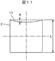
第3の実施例は、図11に示すように、基板側ランドにランドサイズの0.1倍以上の深さの、凹みを設けるものである。図11において、ランドサイズはLであり、凹みの量はRである。すなわち、Rは0.1Lよりも大きくする。これによって、溶融半田表面22にさらに広い凹面が形成できる。
この凹み部深さはランドサイズの0.2倍程度を超えると、ランド角部へ半田ぬれ拡がりが困難となるため、凹みの深さはランドサイズの0.1乃至0.2倍程度が望ましい。また、この凹みを、曲率半径の小さい曲線や急な角度で曲がる折れ線で凹みを形成すると、半田がその形状に倣ってぬれ拡がることが困難になる。そのため、凹みはなるべく滑らかな形状である必要がある。なお、この滑らかな凹みは、一本の二次曲線や円弧、あるいはこれら複数を滑らかにつなげて形成することが可能である。
以下に本実施例の具体的なプロセスを示す。すなわち、部品電極ピッチ:1.2mm、部品電極形状:正方形、部品電極サイズ:0.7mm、部品電極数:90(9行10列)のランドグリッドアレイ10、および、半田合金組成:Sn-3Ag-0.5Cuの半田ペースト20を用いて、半田ペースト印刷厚:0.15mmとしてリフロー半田付けを実施した。半田付けに使用したプリント基板は、基板基材:FR-4、基板厚:1.6mm、ランド銅箔厚:18μmのものを用意した。
なお、基板のランド配置は、ランドピッチ、ランド形状、ランドサイズが、ランドグリッドアレイ10と同じで、ランド外周の4辺がランド配列方向に平行なもの(従来仕様C)と、全基板のランドの一辺に0.12mmの深さの一つの円弧で形成した凹みを設けたもの(改良仕様C)を用意した。
従来仕様Cを100個と改良仕様Cを100個、リフロー半田付け後、全ての半田接続部のX線透視観察を実施した。その結果、残留する気泡100について、その上位10%の直径の平均値は、従来仕様Cについては、0.48mmになったが、改良仕様Cについては、0.35mmになった。
また、-55~125℃、1サイクル/時の条件で温度サイクル試験を実施した。その結果、従来仕様Cにおいて、気泡100が全く存在しない場合の寿命が約1050サイクルではあるが、平均寿命は約500サイクルになった。一方、改良仕様Cの平均寿命は約750サイクルになった。よって、本案を適用した改良仕様Cの場合、その平均寿命が改善されていることがわかった。
また、基板側ランドの凹みの深さをランドサイズの0.15倍とし、この凹みを1種類の円弧で形成した場合、巨大な気泡100はこの凹み部より、自然に排出され、残留する気泡100については、その上位10%の直径の平均値がランドサイズの概ね0.5倍程度になるという結果を得た。
また、温度サイクル試験により、半田接続部に熱機械的ストレスを与える試験を実施すると、気泡100が全く存在しない場合の寿命をLとすると、平均寿命は0.7L程度になった。しかし、本案を適用しない場合、多くの接続部に巨大なボイドの残留があり、その平均寿命0.5Lであるので、これと比較すると信頼性は大幅に改善されていることになる。
本実施例は以上で説明した実施例1~実施例3を組み合わせることである。これによって、上記実施例1~実施例3を単独で実施する場合よりも効果を上げることも可能である。
図12は実施例1と実施例3を組み合わせた例である。図12(a)は回路基板電極2と部品電極11が合わされた状態の平面図であり、図12(b)は図12(a)の部分詳細図である。図12(a)において、回路基板電極2は点線で示す部品電極11に対してθ度傾いている。また、回路基板電極2の1辺において、ランドサイズLに対して0.1倍の深さの凹みを設けている。
このことにより、回路基板電極2と部品電極11を傾けた効果と回路基板電極2に凹部を形成した効果とがあいまって、実施例1あるいは実施例3の場合よりもより、溶融半田表面22には、大きな凹部が形成される。したがって、残留する気泡100の大きさも、より小さくすることが出来る。
図12では、P点の両側に曲率半径の異なる2種類の円弧を滑らかに繋げた曲線で凹みを形成している。すなわち、図12(b)において、曲線3は第1の円弧であり、曲線4は第2の円弧であり、第1の円弧と第2の円弧は曲率半径が異なっている。しかし、電極中心を通り、傾きθ/2度の直線と、曲線3および曲線4は1点で交わるようにしている。そして、このときの深さQは0.1Lである。
図12に示す構成においては、気泡100はこの凹み部より、自然に排出され、残留する気泡100については、その上位10%の直径の平均値がランドサイズの概ね0.3倍程度になる。温度サイクル試験により、半田接続部に熱機械的ストレスを与える試験を実施すると、気泡100が全く存在しない場合の寿命をLとすると、平均寿命は0.8L程度になった。しかし、本案を適用しない場合、多くの接続部に巨大なボイドの残留があり、その平均寿命0.5Lであるので、信頼性は大きく改善されていることになる。
本実施例の具体的なプロセスは次のとおりである。部品電極ピッチ:1.2mm、部品電極形状:正方形、部品電極サイズ:0.7mm、部品電極数:77のランドグリッドアレイ10、および、半田合金組成:Sn-3Ag-0.5Cuの半田ペースト20を用いて、半田ペースト印刷厚:0.15mmとしてリフロー半田付けを実施した。半田付けに使用したプリント基板は、基板基材:FR-4、基板厚:1.6mm、ランド銅箔厚:18μmのものを用意した。
基板のランド配置は、ランドピッチ、ランド形状、ランドサイズが、ランドグリッドアレイ10と同じで、基板のランドをその中心を軸にして18°回転させた位置に移したもの(改良仕様A)と、この改良仕様Aのランドの一辺に0.12mmの深さの二種類の円弧を滑らかに繋いで形成した凹みを設けたもの(改良仕様A‘)を用意した。
改良仕様Aを100個と改良仕様A‘を100個、リフロー半田付け後、全ての半田接続部のX線透視観察を実施した。その結果、残留する気泡100について、その上位10%の直径の平均値は、改良仕様Aについては、0.35mmになったが、改良仕様A‘については、0.20mmになった。
また、-55~125℃、1サイクル/時の条件で温度サイクル試験を実施した。その結果、改良仕様Aの平均寿命は約1100サイクルであったが、改良仕様A‘の平均寿命は約1200サイクルになった。よって、本案を適用した改良仕様A‘の場合、その平均寿命がさらに改善されていることがわかった。
さらに、上記実施例1~実施例4においては、各々の基板側電極はエッチングで個々に分離することにより形成された物であるが、該回路基板に接続されるランドグリッドアレイは、その種類によっては、放熱効率を高めることや基板側電極と基板基材との接着強度を高める必要性がある。
このことを考慮して、該回路基板側の電極で、各信号端子と接続される電極の中で、同じ信号が流れる少なくとも2つの電極は、ソルダレジスト供給により分割されているだけの1枚の金属箔によって形成されていることがある。このような構成は、ランドグリッドアレイが、DC-DCコンバータ、トランジスタアレイ、あるいは受動部品の集合体のような部品であり、電極のいくつかは同じ信号を流して使用する部品である場合には、該電極を1枚の金属箔で形成できるため、有効な手段である。
しかし、同じ信号を流して使用するランドグリッドアレイ側の各信号端子、同じ信号を流して使用する回路基板側の電極を、各々大きな1枚の金属箔によって形成しこのまま使用すると、はんだ接続部内に残留するフラックスアウトガス起因のボイドのサイズは接続部のサイズに相関して大きくなる。また、さらに、ボイドの発生位置が接続部中央部付近になるほど、接続部内に残留しやすくなるというデメリットがあり、はんだ接続部の強度が低下するため、接続信頼性上良くない。一方、この手段により、基板側の電極面積を広くすることが可能となり、部品内で発生した熱量を基板基材内への短時間で伝えることができるようになるため、放熱性を高めることが可能になるというメリットがある。
図13は、ランドグリッドアレイ10を接続する該回路基板1側の電極の入力端子群、出力端子群および、グランド端子群の各々が、3枚の金属箔(回路基板電極2)を回路基板1に供給したソルダレジスト30の開口部31により分割形成されている様子を示した図である。本実施例は、実施例4に上記の考え方を組み合わせた例である。これによって、実施例4を単独で実施する場合と比較すれば、放熱効率を高めることや基板側電極と基板基材との接着強度効果を上げることが可能となる。
図14は実施例4に上記の考え方を組み合わせた一例を示した図である。図14は、図13における該回路基板電極上に供給されたソルダレジスト30における開口部31の形状を変更することによって形づくられている。また、該回路基板側の電極の入力端子、出力端子および、グランド端子の各々の形状、すなわちソルダレジスト開口部31の形状は、図12(b)と同一形状としている。
従って、本実施例は具体的には次のとおりとなる。すなわち、部品電極ピッチ:1.2mm、部品電極形状:正方形、部品電極サイズ:0.7mm、部品電極数:77のランドグリッドアレイ10、および、半田合金組成:Sn-3Ag-0.5Cuの半田ペースト20を用いて、半田ペースト印刷厚:0.15mmとしてリフロー半田付けを実施した。半田付けに使用したプリント基板は、基板基材:FR-4、基板厚:1.6mm、ランド銅箔厚:18μmのものを用意した。
基板のランド配置は、ランドピッチ、ランド形状、ランドサイズが、ランドグリッドアレイ10と同じで、基板のランドをその中心を軸にして18°回転させた位置に移し、この基板ランドの一辺に0.12mmの深さの二種類の円弧を滑らかに繋いで形成した凹みを設けており、上記ランド形状は銅箔をエッチングすることによって個々に分離して形成したもの(実施例4で使用したものと同一の、改良仕様A‘)、を用意した。
また、これと比較するため、ランドグリッドアレイを接続する該回路基板側の電極の入力端子群、出力端子群および、グランド端子群の各々が、ソルダレジスト供給により分割されているだけの1枚の金属箔によって形成されており、各々のランドはソルダレジストを供給しない部分の形状を改良仕様A‘と同一にすることによって作製したもの(改良仕様A“)も用意した。
改良仕様A‘を100個と改良仕様A“を100個、リフロー半田付け後、全てのはんだ接続部のX線透視観察を実施した。その結果、残留する気泡100について、その上位10%の直径の平均値は、改良仕様A‘、A“ともに、0.20mmになった。
また、-55~125℃、1サイクル/時の条件で温度サイクル試験を実施した。その結果、改良仕様A‘、A“ともに、平均寿命は約1200サイクルであり、接続信頼性は損なわれることがないことがわかった。
さらに、本ランドグリッドアレイ稼動時のパッケージ表面温度を同一気温条件化で測定したところ、改良仕様A‘では、51℃であるのに対して、A“では、46℃であることがわかり、該回路基板側の電極の入力端子群、出力端子群および、グランド端子群の各々が、ソルダレジスト供給により分割されているだけの1枚の金属箔によって形成することにより、部品で発生した熱の基板への放熱性能が向上していることも確認できた。
以上説明したように、本実施例を適用し、ランドグリッドアレイを接続する回路基板側の電極を、銅箔エッチングによって個々に電極を分離して形成せずに、該回路基板側の電極の入力端子群、出力端子群および、グランド端子群の各々が、ソルダレジスト供給により分割されているだけの1枚の金属箔によって形成すれば、接続信頼性を損なうことなく部品で発生した熱の基板への放熱性能を向上できる。
以上説明したように、本実施例を適用し、ランドグリッドアレイを接続する回路基板側の電極を、銅箔エッチングによって個々に電極を分離して形成せずに、該回路基板側の電極の入力端子群、出力端子群および、グランド端子群の各々が、ソルダレジスト供給により分割されているだけの1枚の金属箔によって形成すれば、接続信頼性を損なうことなく部品で発生した熱の基板への放熱性能を向上できる。
1・・・回路基板
2・・・回路基板ランド(回路基板電極)
3・・・第1の円弧
4・・・第2の円弧
10・・・ランドグリッドアレイ
11・・・ランドグリッドアレイ電極(部品電極)
20・・・半田ペースト
21・・・溶融半田
22・・・溶融半田表面
23・・・溶融半田(薄皮状部分)
30・・・ソルダレジスト
31・・・ソルダレジスト開口部
100・・・気泡。
2・・・回路基板ランド(回路基板電極)
3・・・第1の円弧
4・・・第2の円弧
10・・・ランドグリッドアレイ
11・・・ランドグリッドアレイ電極(部品電極)
20・・・半田ペースト
21・・・溶融半田
22・・・溶融半田表面
23・・・溶融半田(薄皮状部分)
30・・・ソルダレジスト
31・・・ソルダレジスト開口部
100・・・気泡。
Claims (14)
- 部品電極がマトリクス状に形成されたランドグリッドアレイと回路基板電極がマトリクス状に形成された回路基板がリード線を用いないで半田によって直接接続された回路基板構造体であって、
前記回路基板電極は前記部品電極に対して、平面で見て所定の角度回転していることを特徴とする回路基板構造体。 - 前記回路基板電極は、前記部品電極に対して15度~20度回転していることを特徴とする請求項1に記載の回路基板構造体。
- 部品電極がマトリクス状に形成されたランドグリッドアレイと回路基板電極がマトリクス状に形成された回路基板がリード線を用いないで半田によって直接接続された回路基板構造体であって、
前記回路基板電極の中心は、前記部品電極の中心に対して、所定の距離ずれており、半田が溶融したときに、前記回路基板および前記ランドグリッドアレイに働く力がゼロになるように、前記ずれている方向が複数となっていることを特徴とする回路基板構造体。 - 部品電極がマトリクス状に形成されたランドグリッドアレイと回路基板電極がマトリクス状に形成された回路基板がリード線を用いないで半田によって直接接続された回路基板構造体であって、
前記回路基板電極の中心は、前記部品電極の中心に対して、所定の距離ずれており、
前記ずれの方向は、前記マトリクス状に形成された回路基板電極の中心線に対して、左右、または、上下に対して逆方向であることを特徴とする回路基板構造体。 - 前記ずらす量は、回路基板電極のずらす方向に辺の1/8以上1/4以下であることを特徴とする請求項4に記載の回路基板構造体。
- 部品電極がマトリクス状に形成されたランドグリッドアレイと回路基板電極がマトリクス状に形成された回路基板がリード線を用いないで半田によって直接接続された回路基板構造体であって、
前記回路基板電極の中心は、前記部品電極の中心に対して、所定の距離ずれており、
前記ずれの方向は、前記マトリクス状に形成された回路基板電極の中心線に対して、左右、および、上下に対して逆方向であることを特徴とする回路基板構造体。 - 前記ずらす量は、回路基板電極のずらす方向に辺の1/8以上1/4以下であることを特徴とする請求項6に記載の回路基板構造体。
- 部品電極がマトリクス状に形成されたランドグリッドアレイと回路基板電極がマトリクス状に形成された回路基板がリード線を用いないで半田によって直接接続された回路基板構造体であって、
前記回路基板電極における辺は、外方向に凹形状となっていることを特徴とする回路基板構造体。 - 前記凹形状の量は、前記回路基板電極の前記凹形状となっている辺と直角方向の辺の長さの0.1倍~0.2倍であることを特徴とする請求項7に記載の回路基板構造体。
- 部品電極がマトリクス状に形成されたランドグリッドアレイと回路基板電極がマトリクス状に形成された回路基板がリード線を用いないで半田によって直接接続された回路基板構造体であって、
前記回路基板電極は前記部品電極に対して、平面で見て所定の角度回転しており、
前記回路基板電極における辺は、外方向に凹形状となっていることを特徴とする回路基板構造体。 - 部品電極がマトリクス状に形成されたランドグリッドアレイと回路基板電極がマトリクス状に形成された回路基板がリード線を用いないで半田によって直接接続された回路基板構造体であって、
前記回路基板電極の中心は、前記部品電極の中心に対して、所定の距離ずれており、半田が溶融したときに、前記回路基板および前記ランドグリッドアレイに働く力がゼロになるように、前記ずれている方向が複数となっており、
前記回路基板電極における辺は、外方向に凹形状となっていることを特徴とする回路基板構造体。 - 前記回路基板電極の形状は、前記回路基板電極上に供給されたソルダレジストの供給形状によって形づくられ、前記ソルダレジストが供給されない開口部を設けることで、前記回路基板電極を表面に露出させることによってパターン形成されていることを特徴とする請求項1から請求項11のいずれか1項に記載の回路基板構造体。
- 前記回路基板に接続される前記ランドグリッドアレイは、DC-DCコンバータ、トランジスタアレイ、あるいは受動部品などの集合体であり、各信号端子と接続される電極の中で、同じ信号が流れる少なくとも2つの前記回路基板側の電極は前記ソルダレジストにより分割されているだけの1枚の金属箔によって形成されていることを特徴とする請求項12に記載の回路基板構造体。
- 前記回路基板に接続される前記ランドグリッドアレイは、その電極の大部分が入力、出力、およびグランドの信号端子となる前記DC-DCコンバータであり、前記DC-DCコンバータの入力、出力、グランド等、各信号端子と接続される前記回路基板側の電極の中で、同じ信号が流れる少なくとも2つの電極は前記ソルダレジストにより分割されているだけの1枚の金属箔によって形成されていることを特徴とする請求項13に記載の回路基板構造体。
Applications Claiming Priority (4)
| Application Number | Priority Date | Filing Date | Title |
|---|---|---|---|
| JP2009026048 | 2009-02-06 | ||
| JP2009-026048 | 2009-02-06 | ||
| JP2009-279594 | 2009-12-09 | ||
| JP2009279594A JP2010206166A (ja) | 2009-02-06 | 2009-12-09 | 回路基板構造体 |
Publications (1)
| Publication Number | Publication Date |
|---|---|
| WO2010089963A1 true WO2010089963A1 (ja) | 2010-08-12 |
Family
ID=42541876
Family Applications (1)
| Application Number | Title | Priority Date | Filing Date |
|---|---|---|---|
| PCT/JP2010/000328 Ceased WO2010089963A1 (ja) | 2009-02-06 | 2010-01-21 | 回路基板構造体 |
Country Status (2)
| Country | Link |
|---|---|
| JP (1) | JP2010206166A (ja) |
| WO (1) | WO2010089963A1 (ja) |
Cited By (1)
| Publication number | Priority date | Publication date | Assignee | Title |
|---|---|---|---|---|
| US20220302059A1 (en) * | 2021-03-19 | 2022-09-22 | Tdk Corporation | Electronic component and manufacturing method thereof, and manufacturing method for mounting board |
Citations (6)
| Publication number | Priority date | Publication date | Assignee | Title |
|---|---|---|---|---|
| JPH0951017A (ja) * | 1995-08-04 | 1997-02-18 | Fujitsu Ltd | 半導体モジュール |
| JPH0974267A (ja) * | 1995-09-04 | 1997-03-18 | Matsushita Electric Ind Co Ltd | 回路基板 |
| JPH1117319A (ja) * | 1997-06-26 | 1999-01-22 | Matsushita Electric Ind Co Ltd | チップの実装方法 |
| JPH11145198A (ja) * | 1997-11-10 | 1999-05-28 | Toshiba Corp | 半導体装置 |
| JP2001060759A (ja) * | 1999-08-19 | 2001-03-06 | Yaskawa Electric Corp | 電子部品のボール端子接続構造 |
| JP2001156432A (ja) * | 1999-11-29 | 2001-06-08 | Opnext Japan Inc | モジュール及び電子部品の実装方法 |
-
2009
- 2009-12-09 JP JP2009279594A patent/JP2010206166A/ja active Pending
-
2010
- 2010-01-21 WO PCT/JP2010/000328 patent/WO2010089963A1/ja not_active Ceased
Patent Citations (6)
| Publication number | Priority date | Publication date | Assignee | Title |
|---|---|---|---|---|
| JPH0951017A (ja) * | 1995-08-04 | 1997-02-18 | Fujitsu Ltd | 半導体モジュール |
| JPH0974267A (ja) * | 1995-09-04 | 1997-03-18 | Matsushita Electric Ind Co Ltd | 回路基板 |
| JPH1117319A (ja) * | 1997-06-26 | 1999-01-22 | Matsushita Electric Ind Co Ltd | チップの実装方法 |
| JPH11145198A (ja) * | 1997-11-10 | 1999-05-28 | Toshiba Corp | 半導体装置 |
| JP2001060759A (ja) * | 1999-08-19 | 2001-03-06 | Yaskawa Electric Corp | 電子部品のボール端子接続構造 |
| JP2001156432A (ja) * | 1999-11-29 | 2001-06-08 | Opnext Japan Inc | モジュール及び電子部品の実装方法 |
Cited By (3)
| Publication number | Priority date | Publication date | Assignee | Title |
|---|---|---|---|---|
| US20220302059A1 (en) * | 2021-03-19 | 2022-09-22 | Tdk Corporation | Electronic component and manufacturing method thereof, and manufacturing method for mounting board |
| CN115119395A (zh) * | 2021-03-19 | 2022-09-27 | Tdk株式会社 | 电子部件及其制造方法、和安装基板的制造方法 |
| US12532768B2 (en) * | 2021-03-19 | 2026-01-20 | Tdk Corporation | Electronic component having terminal formation area offset from mounting surface center and manufacturing method of same and of mounting board |
Also Published As
| Publication number | Publication date |
|---|---|
| JP2010206166A (ja) | 2010-09-16 |
Similar Documents
| Publication | Publication Date | Title |
|---|---|---|
| EP2633551B1 (en) | Lead-free structures in a semiconductor device | |
| JP2006295156A (ja) | 半導体モジュール及びそれの製造方法 | |
| CN101996902A (zh) | 半导体器件的制造方法 | |
| KR102574011B1 (ko) | 반도체 소자의 실장 구조 및 반도체 소자와 기판의 조합 | |
| CN1790685A (zh) | 带半导体部件的布线基板 | |
| JP4831502B2 (ja) | 耐落下衝撃特性に優れた接続端子用ボールおよび接続端子ならびに電子部品 | |
| TWI333405B (ja) | ||
| JP2011171427A (ja) | 積層型半導体装置 | |
| JP3143441B2 (ja) | 表面実装回路デバイス用のハンダバンプ入力/出力パッド | |
| CN100473259C (zh) | 电路板组装方法与结构及用以组装该结构的工装用具 | |
| JP2017022190A (ja) | 実装構造体 | |
| WO2010089963A1 (ja) | 回路基板構造体 | |
| JP3942952B2 (ja) | リフロー半田付け方法 | |
| CN100593239C (zh) | 芯片及其制造方法 | |
| JP2005268346A (ja) | 半導体パッケージ基板とその製造方法 | |
| JP2019054115A (ja) | 半導体装置の製造方法 | |
| JP2016162813A (ja) | プリント基板及びハンダ付け方法 | |
| US6531664B1 (en) | Surface mount devices with solder | |
| JP2005072212A (ja) | 電子部品とその製造方法及び電子装置 | |
| JP2008140868A (ja) | 多層配線基板および半導体装置 | |
| JP4906563B2 (ja) | 半導体装置及び配線基板、並びにそれらの製造方法 | |
| CN1980525A (zh) | 连接元器件焊脚的线路板焊盘及其连接结构和连接方法 | |
| JP2019062000A (ja) | スクリーン印刷用マスク、及びプリント配線基板 | |
| JP2008218483A (ja) | 半導体装置及びその製造方法 | |
| JP2006066811A (ja) | はんだ印刷用マスク、部品実装方法 |
Legal Events
| Date | Code | Title | Description |
|---|---|---|---|
| 121 | Ep: the epo has been informed by wipo that ep was designated in this application |
Ref document number: 10738307 Country of ref document: EP Kind code of ref document: A1 |
|
| NENP | Non-entry into the national phase |
Ref country code: DE |
|
| 122 | Ep: pct application non-entry in european phase |
Ref document number: 10738307 Country of ref document: EP Kind code of ref document: A1 |