WO2010061839A1 - 駆動回路、表示装置および駆動回路の自己検出・自己修復方法 - Google Patents
駆動回路、表示装置および駆動回路の自己検出・自己修復方法 Download PDFInfo
- Publication number
- WO2010061839A1 WO2010061839A1 PCT/JP2009/069839 JP2009069839W WO2010061839A1 WO 2010061839 A1 WO2010061839 A1 WO 2010061839A1 JP 2009069839 W JP2009069839 W JP 2009069839W WO 2010061839 A1 WO2010061839 A1 WO 2010061839A1
- Authority
- WO
- WIPO (PCT)
- Prior art keywords
- output
- circuit
- output circuit
- signal
- circuits
- Prior art date
Links
Images


Classifications
-
- G—PHYSICS
- G09—EDUCATION; CRYPTOGRAPHY; DISPLAY; ADVERTISING; SEALS
- G09G—ARRANGEMENTS OR CIRCUITS FOR CONTROL OF INDICATING DEVICES USING STATIC MEANS TO PRESENT VARIABLE INFORMATION
- G09G3/00—Control arrangements or circuits, of interest only in connection with visual indicators other than cathode-ray tubes
- G09G3/20—Control arrangements or circuits, of interest only in connection with visual indicators other than cathode-ray tubes for presentation of an assembly of a number of characters, e.g. a page, by composing the assembly by combination of individual elements arranged in a matrix no fixed position being assigned to or needed to be assigned to the individual characters or partial characters
- G09G3/34—Control arrangements or circuits, of interest only in connection with visual indicators other than cathode-ray tubes for presentation of an assembly of a number of characters, e.g. a page, by composing the assembly by combination of individual elements arranged in a matrix no fixed position being assigned to or needed to be assigned to the individual characters or partial characters by control of light from an independent source
- G09G3/36—Control arrangements or circuits, of interest only in connection with visual indicators other than cathode-ray tubes for presentation of an assembly of a number of characters, e.g. a page, by composing the assembly by combination of individual elements arranged in a matrix no fixed position being assigned to or needed to be assigned to the individual characters or partial characters by control of light from an independent source using liquid crystals
- G09G3/3611—Control of matrices with row and column drivers
- G09G3/3685—Details of drivers for data electrodes
- G09G3/3688—Details of drivers for data electrodes suitable for active matrices only
-
- G—PHYSICS
- G02—OPTICS
- G02F—OPTICAL DEVICES OR ARRANGEMENTS FOR THE CONTROL OF LIGHT BY MODIFICATION OF THE OPTICAL PROPERTIES OF THE MEDIA OF THE ELEMENTS INVOLVED THEREIN; NON-LINEAR OPTICS; FREQUENCY-CHANGING OF LIGHT; OPTICAL LOGIC ELEMENTS; OPTICAL ANALOGUE/DIGITAL CONVERTERS
- G02F1/00—Devices or arrangements for the control of the intensity, colour, phase, polarisation or direction of light arriving from an independent light source, e.g. switching, gating or modulating; Non-linear optics
- G02F1/01—Devices or arrangements for the control of the intensity, colour, phase, polarisation or direction of light arriving from an independent light source, e.g. switching, gating or modulating; Non-linear optics for the control of the intensity, phase, polarisation or colour
- G02F1/13—Devices or arrangements for the control of the intensity, colour, phase, polarisation or direction of light arriving from an independent light source, e.g. switching, gating or modulating; Non-linear optics for the control of the intensity, phase, polarisation or colour based on liquid crystals, e.g. single liquid crystal display cells
-
- G—PHYSICS
- G09—EDUCATION; CRYPTOGRAPHY; DISPLAY; ADVERTISING; SEALS
- G09G—ARRANGEMENTS OR CIRCUITS FOR CONTROL OF INDICATING DEVICES USING STATIC MEANS TO PRESENT VARIABLE INFORMATION
- G09G3/00—Control arrangements or circuits, of interest only in connection with visual indicators other than cathode-ray tubes
- G09G3/006—Electronic inspection or testing of displays and display drivers, e.g. of LED or LCD displays
-
- G—PHYSICS
- G09—EDUCATION; CRYPTOGRAPHY; DISPLAY; ADVERTISING; SEALS
- G09G—ARRANGEMENTS OR CIRCUITS FOR CONTROL OF INDICATING DEVICES USING STATIC MEANS TO PRESENT VARIABLE INFORMATION
- G09G3/00—Control arrangements or circuits, of interest only in connection with visual indicators other than cathode-ray tubes
- G09G3/20—Control arrangements or circuits, of interest only in connection with visual indicators other than cathode-ray tubes for presentation of an assembly of a number of characters, e.g. a page, by composing the assembly by combination of individual elements arranged in a matrix no fixed position being assigned to or needed to be assigned to the individual characters or partial characters
-
- G—PHYSICS
- G09—EDUCATION; CRYPTOGRAPHY; DISPLAY; ADVERTISING; SEALS
- G09G—ARRANGEMENTS OR CIRCUITS FOR CONTROL OF INDICATING DEVICES USING STATIC MEANS TO PRESENT VARIABLE INFORMATION
- G09G2310/00—Command of the display device
- G09G2310/02—Addressing, scanning or driving the display screen or processing steps related thereto
- G09G2310/0264—Details of driving circuits
- G09G2310/027—Details of drivers for data electrodes, the drivers handling digital grey scale data, e.g. use of D/A converters
-
- G—PHYSICS
- G09—EDUCATION; CRYPTOGRAPHY; DISPLAY; ADVERTISING; SEALS
- G09G—ARRANGEMENTS OR CIRCUITS FOR CONTROL OF INDICATING DEVICES USING STATIC MEANS TO PRESENT VARIABLE INFORMATION
- G09G2330/00—Aspects of power supply; Aspects of display protection and defect management
- G09G2330/08—Fault-tolerant or redundant circuits, or circuits in which repair of defects is prepared
Definitions
- the present invention relates to a display device including a drive circuit having a function of performing self-detection and self-repair.
- a liquid crystal display device or the like display is performed by mounting a plurality of drive circuits formed of a semiconductor integrated circuit (LSI) on a display panel, and the drive circuit outputs a gradation voltage to the display panel.
- LSI semiconductor integrated circuit
- the display device when a failure occurs in the drive circuit, the display device is directly recognized as a display failure.
- the display device manufacturer needs to repair the defective part quickly, and it is desirable that the user should finish the repair in a short time at the place where the user is using the display device.
- a control board that processes display signals can be easily replaced because it is connected to the display panel through a connector.
- the drive circuit is directly connected to the display panel without using a connector or the like, it is difficult to replace the drive circuit where the user is using the display device.
- Patent Document 1 discloses a technology in which a drive circuit of a product in which a drive circuit is integrated with a display panel is made redundant so that the drive circuit can be restored even after the product is completed.
- a spare output circuit is provided in the drive circuit, and the output of one output circuit in the drive circuit is compared with the output of the spare output circuit to determine whether the outputs are equal to each other.
- self-detection for confirming that the output circuit is normal is performed, and a technique for driving the display panel with a spare output circuit instead of the output circuit to be detected during self-detection is also disclosed. .
- the output circuit to be detected is separated from the display panel, the display panel is driven by the spare output circuit, and the output of the spare output circuit is compared with the output of the output circuit to be detected.
- the quality of the output circuit to be detected is determined.
- gradation data for display is input simultaneously to the output circuit to be detected and the spare output circuit, data for comparison is limited.
- the display panel data to be driven by the output circuit to be detected should be driven. Since the line is not driven, a display defect occurs.
- the present invention has been made in view of the above problems, and an object of the present invention is to realize a drive circuit capable of detecting a malfunction of an output circuit while driving a display panel without causing a display defect. It is in.
- a drive circuit has n output terminals (n is a natural number of 2 or more) for outputting a video signal to a display device, and means for detecting and repairing its own defect.
- Switching means for selecting p output circuits from the first output circuit, disconnecting the connection from the output terminal, and connecting the p output circuits from the second output circuit to the output terminal;
- the selected first output Comparing means for comparing the video signal from the circuit with the video signal from the third output circuit, and determining whether or not the selected first output circuit is defective based on the comparison result of the comparing means It is characterized by providing the determination means to do.
- the first output circuit is detachably connected to the output terminal, and during the normal operation, all the first output circuits are connected to the data line by the switching means, and the second output circuit The output circuit is not connected to the data line.
- the switching means disconnects the connection between the selected first output circuit and the output terminal, and connects the second output circuit to the output terminal.
- the comparison means compares the video signal from the selected first output circuit disconnected from the output terminal with the video signal from the third output circuit, and the determination means determines the comparison result. Based on the above, it is determined whether or not the selected first output circuit is defective.
- the first output circuit and the second output circuit excluding the selected first output circuit are connected to the output terminal, and these output circuits drive the display panel.
- the second output circuit drives the display panel instead of the selected first output circuit to be detected, the output is performed while driving the display panel without causing a display defect.
- the switching means is rth (r is less than q).
- the r-th first output circuit is connected to the output terminal of s + pth and the s + p-th first output is connected to the s-th output terminal (s is a natural number greater than or equal to q and less than or equal to np).
- the second output circuit is connected to the t-th output terminal (t is a natural number greater than np and less than or equal to n).
- the output of the last column is output from the output circuit of the next column of the selected first output circuit at the time of self-detection.
- Each output circuit up to the circuit outputs a video signal to each output terminal to which each output circuit from the selected first output circuit to the output circuit in the previous row of the output circuit in the last row is connected during normal driving.
- the second output circuit outputs a video signal to an output terminal to which the output circuit in the last column is connected during normal driving during self-detection.
- the output circuit adjacent to the output circuit connected at the time of normal driving is connected to the output terminal of the previous column of the last column from the output terminal connected at the time of normal driving of the selected first output circuit.
- a second output circuit is connected to the output terminal.
- the switching means connects the output terminal from which the selected first output circuit is disconnected and the second output circuit.
- the second output circuit outputs a video signal to the output terminal to which the selected first output circuit is connected during normal driving during self-detection. Therefore, even at the time of self-detection, the display panel can be driven without causing a display defect by the first output circuit and the second output circuit excluding the selected first output circuit.
- the drive circuit according to the present invention includes control means for inputting the input data to the first to third output circuits via a data bus to which the input data is supplied, and the control means is selected as described above. It is preferable that the input data input to the first output circuit and the input data input to the third output circuit are controlled so as to have different values.
- the data bus is composed of first to third data buses, and the control means sends the selected first output circuit via the first data bus.
- the input data is input to the first output circuit excluding the second output circuit, the input data is input to the selected first output circuit via the second data bus, and It is preferable to input the input data to the third output circuit via a third data bus.
- input data for self-detection can be supplied via the second data bus and the third data bus. Therefore, the time for self-detection can be shortened compared to the case where input data is supplied via one data bus.
- control means inputs the input data to the first to third output circuits via one data bus.
- the area of the drive circuit can be reduced as compared with the case where a plurality of data buses are provided.
- the video signal is a gradation voltage
- the first to third output circuits include a digital-analog converter that converts the input data into the gradation voltage
- the comparison unit includes The gradation voltage from the digital / analog converter provided in the selected first output circuit may be compared with the gradation voltage from the digital / analog converter provided in the third output circuit.
- the first output circuit includes an operational amplifier as an output buffer of the digital-analog converter, and the operational amplifier has the first output circuit including the operational amplifier selected by the switching unit. It is preferable that the comparator operates as a comparator when not connected to the output terminal, and the comparison means is an operational amplifier that operates as the comparator.
- the operational amplifier provided in the first output circuit can be used as the comparison means, it is not necessary to provide the comparison means separately from the first output circuit. Therefore, the area of the drive circuit can be reduced.
- the third output circuit is connected to an operational amplifier that operates as the comparator.
- the operational amplifier can compare the gradation voltage from the selected first output circuit with the gradation voltage from the third output circuit.
- the operational amplifier preferably operates as a voltage follower when a first output circuit including the operational amplifier is connected to the output terminal.
- the determination means uses the comparison result from the comparison means corresponding to the input data respectively input to the selected first output circuit and the third output circuit as an expected value.
- the comparison result and the expected value are different, it is preferable to determine that the selected first output circuit is defective.
- an input signal of gradation m is input to the selected first output circuit, and an input signal of gradation m + 1 is input to the third output circuit.
- the gradation voltage of gradation m is lower than the gradation voltage of gradation m + 1.
- the comparison means outputs a signal indicating that the gradation voltage input from the third output circuit is higher.
- the comparing means is selected. A signal indicating that the input gradation voltage is higher than that of the first output circuit is output.
- the comparison unit compares the gradation voltages output from the selected first output circuit and the third output circuit, and the selected first output circuit is defective or not. , Outputs signals of different values. Further, the determining means determines whether or not the selected first output circuit is defective based on the signal output from the comparing means. Specifically, as described above, the input signal of gradation m is input to the selected first output circuit, and the input signal of gradation m + 1 is input to the third output circuit. When a signal indicating that the gradation voltage from the first output circuit is high is input from the comparison means, it is determined that the selected first output circuit is defective. On the other hand, when a signal indicating that the gradation voltage from the third output circuit is high is input from the comparison unit, the determination unit determines that the selected first output circuit is not defective.
- a drive circuit is a drive circuit having n (n is a natural number of 2 or more) output terminals for outputting a video signal to a display device, and means for detecting and repairing its own defect.
- n is a natural number of 2 or more
- u or more u is an even number of 2 or more and n or less
- second output circuits and u output circuits are selected from the first output circuit, and the connection to the output terminal is disconnected, and the second output circuit is selected.
- Switching means for connecting u output circuits from the output circuit to the output terminal, and any two of the selected first output circuits as a first selection output circuit and a second selection output circuit, From the first selection output circuit Comparison means for comparing the image signal with the video signal of the second selection output circuit, and determination means for determining whether the selected first output circuit is defective based on the comparison result of the comparison means It is characterized by comprising.
- the first output circuit is detachably connected to the output terminal, and during the normal operation, all the first output circuits are connected to the output terminal by the switching means, and the second output circuit is connected to the second output circuit.
- the output circuit is not connected to the output terminal.
- the switching unit disconnects the selected u first output circuits from the output terminals, and connects the u second output circuits to the output terminals.
- the comparison means compares the two video signals from the first selection output circuit and the second selection output circuit among the selected first output circuits separated from the output terminal, and A determination unit determines whether or not the selected first output circuit is defective based on the comparison result.
- the first output circuit and the second output circuit excluding the selected first output circuit are connected to the output terminal, and these output circuits drive the display panel.
- the second output circuit drives the display panel instead of the selected first output circuit to be detected, the output is performed while driving the display panel without causing a display defect.
- the switching means is the wth (w is a natural number less than v).
- the w-th first output circuit is connected to the output terminal, and the x + u-th first output circuit is connected to the x-th (x is a natural number between v and nu).
- the second output circuit is preferably connected to the y-th output terminal (y is a natural number greater than n ⁇ u and less than n).
- the output circuit of the next column on the rear column side among the selected first output circuits at the time of self-detection the output circuits from the output circuit of the last column to the output circuit of the last column are connected to the output terminals to which the output circuits from the selected first output circuit to the output circuit of the last column of the last column are connected during normal driving.
- Output video signal the two second output circuits output a video signal to an output terminal to which the last-row output circuit and the previous-row output circuit are connected during normal driving.
- the output circuit adjacent to the output circuit connected at the time of normal driving is connected to the output terminal from the output terminal to which the selected first output circuit is connected at the time of normal driving to the last row before the last column.
- the second output circuit is connected to the output terminal of the last column and the preceding column.
- the switching means connects the output terminal from which the selected first output circuit is disconnected and the second output circuit.
- the second output circuit outputs a video signal to the output terminal to which the selected first output circuit is connected during normal driving during self-detection. Therefore, even at the time of self-detection, the display panel can be driven without causing a display defect by the first output circuit and the second output circuit excluding the selected first output circuit.
- the drive circuit according to the present invention includes control means for inputting the input data to the first and second output circuits, and the control means includes input data input to the first selection output circuit, and It is preferable to perform control so that the input data input to the second selection output circuit is different from the input data.
- the video signal is a gradation voltage
- the first output circuit includes a digital-analog converter that converts the input data into the gradation voltage
- the comparing means includes the first signal.
- the gradation voltage from the digital / analog converter provided in one selection output circuit may be compared with the gradation voltage from the digital / analog converter provided in the second selection output circuit.
- the first output circuit includes an operational amplifier as an output buffer of the digital-analog converter, and the operational amplifier has the first output circuit including the operational amplifier selected by the switching unit. It is preferable that the comparator operates as a comparator when not connected to the output terminal, and the comparison means is an operational amplifier that operates as the comparator.
- the operational amplifier provided in the first output circuit can be used as the comparison means, it is not necessary to provide the comparison means separately from the first output circuit. Therefore, the area of the drive circuit can be reduced.
- the operational amplifier preferably operates as a voltage follower when a first output circuit including the operational amplifier is connected to the output terminal.
- the determination means uses the comparison result from the comparison means corresponding to input data input to the first selection output circuit and the second selection output circuit as an expected value. It is preferable to determine that the selected first output circuit is defective when the comparison result is different from the expected value.
- an input signal of gradation m is input to the first selection output circuit, and an input signal of gradation m + 1 is input to the second selection output circuit.
- the gradation voltage of gradation m is lower than the gradation voltage of gradation m + 1.
- the comparison means outputs a signal indicating that the gradation voltage input from the second selection output circuit is higher.
- the comparing means determines whether one of the selected first output circuits is defective and the selected first output circuit can output only a high gradation voltage even if a signal of gradation m is input.
- the comparison unit compares the grayscale voltages output from the first selection output circuit and the second selection output circuit, and the selected first output circuit may or may not be defective. And outputs signals of different values.
- the determination unit determines whether any of the selected first output circuits is defective based on the signal output from the comparison unit. Specifically, as described above, when the input signal of gradation m is input to the first selection output circuit and the input signal of gradation m + 1 is input to the second selection output circuit, the first selection is performed. When a signal indicating that the gradation voltage from the output circuit is high is input from the comparison means, it is determined that one of the selected first output circuits is defective. On the other hand, when a signal indicating that the gradation voltage from the second selection output circuit is high is input from the comparison unit, the determination unit determines that the selected first output circuit is not defective.
- the drive circuit includes control means for inputting the input data to the first and second output circuits, and the control means includes input data input to the first selection output circuit, and Control is performed so that the input data input to the second selection output circuit is different from the input data, and the first output circuit includes a sampling circuit that captures and holds the input data in a time-sharing manner, A hold circuit that takes the input data held in the sampling circuit in a time-sharing manner and outputs the input data to the digital-analog converter, and the control means inputs the input data to the sampling circuit during normal driving and performs self-detection.
- the input data may be input to the digital-analog converter of the selected first output circuit.
- a display device is characterized by including the drive circuit.
- the drive circuit self-detection / self-repair method includes n output terminals (n is a natural number of 2 or more) for outputting a video signal to the display device, input data is converted into a video signal, and the output N number of first output circuits detachably connected to the terminals, and p or more (p is 1 or more and n or less) detachably connected to the output terminals while converting input data into video signals
- Self-detection / self-repair method for detecting and repairing a defect in a drive circuit comprising a second output circuit of a natural number) and a third output circuit that is not connected to the output terminal and converts input data into a video signal And selecting p output circuits from the first output circuit, disconnecting the connection between the selected first output circuit and the output terminal, and removing p connections from the second output circuit.
- Output circuit to the output terminal A switching step to be continued; a comparison step for comparing the video signal from the selected first output circuit with a video signal from the third output circuit; and the selection based on a comparison result of the comparison step. And a determination step for determining whether or not the first output circuit is defective.
- the first output circuit is detachably connected to the output terminal, and during normal operation, all the first output circuits are connected to the output terminal, and the second output circuit is connected to the output terminal. Not connected to terminal.
- the switching step the connection between the selected first output circuit and the output terminal is disconnected, and the second output circuit is connected to the output terminal.
- the comparison step the video signal from the selected first output circuit in a state disconnected from the output terminal is compared with the video signal from the third output circuit, and in the determination step, a selection is made based on the comparison result. It is determined whether the first output circuit thus made is defective.
- the first output circuit and the second output circuit excluding the selected first output circuit are connected to the output terminal, and these output circuits drive the display panel.
- the second output circuit drives the display panel instead of the selected first output circuit to be detected, the output is performed while driving the display panel without causing a display defect. A circuit failure can be detected.
- the drive circuit self-detection / self-repair method includes n output terminals (n is a natural number of 2 or more) for outputting a video signal to the display device, input data is converted into a video signal, and the output N number of first output circuits detachably connected to the terminal and u or more (u is 2 or more and n or less) connected to the output terminal so as to convert the input data into a video signal.
- the first output circuit is detachably connected to the output terminal, and during normal operation, all the first output circuits are connected to the output terminal, and the second output circuit is connected to the output terminal. Not connected to terminal.
- the switching step the connection between the selected first output circuit and the output terminal is disconnected, and the second output circuit is connected to the output terminal.
- the comparison step the video signal from one of the selected first output circuits in a state disconnected from the output terminal is compared with the video signal from the other.
- the determination step the video signal is selected based on the comparison result. It is determined whether or not the first output circuit is defective.
- the first output circuit and the second output circuit excluding the selected first output circuit are connected to the output terminal, and these output circuits drive the display panel.
- the second output circuit drives the display panel instead of the selected first output circuit to be detected, the output is performed while driving the display panel without causing a display defect. A circuit failure can be detected.
- the driving device is a driving circuit having n output terminals (n is a natural number of 2 or more) for outputting a video signal to the display device and means for detecting and repairing its own defect.
- the input data is converted into a video signal, and the n first output circuits connected to the output terminal so as to be separable, and the input data is converted into a video signal and can be separated into the output terminal.
- the drive circuit according to the present invention is a drive circuit having n output terminals (n is a natural number of 2 or more) for outputting a video signal to the display device and means for detecting and repairing its own defect.
- the input data is converted into a video signal, and the n first output circuits connected to the output terminal so as to be separable, and the input data is converted into a video signal and can be separated into the output terminal.
- switching means for connecting u output circuits from the second output circuit to the output terminal, and any two of the selected first output circuits are connected to the first selection output circuit and the second output circuit.
- the first selection A comparison means for comparing the video signal from the input circuit with the video signal of the second selection output circuit, and whether the selected first output circuit is defective based on the comparison result of the comparison means.
- determining means for determining.
- the drive circuit self-detection / self-repair method converts n (n is a natural number of 2 or more) output terminals for outputting video signals to the display device, and converts input data into video signals.
- n or more first output circuits that are detachably connected to the output terminals, and p or more (p Self-detecting and repairing a defect in a drive circuit comprising a second output circuit having a natural number between 1 and n and a third output circuit that is not connected to the output terminal and converts input data into a video signal
- p output circuits are selected from the first output circuit, the connection between the selected first output circuit and the output terminal is disconnected, and the second output is selected.
- P output circuits from the circuit A switching step for connecting to the output terminal, a comparison step for comparing the video signal from the selected first output circuit with a video signal from the third output circuit, and a comparison result of the comparison step. And a determination step for determining whether or not the selected first output circuit is defective.
- the drive circuit self-detection / self-repair method converts n (n is a natural number of 2 or more) output terminals for outputting video signals to the display device, and converts input data into video signals. And n or more first output circuits detachably connected to the output terminal, and u or more (u) connected to the output terminal in a separable manner while converting input data into a video signal.
- Is a self-detection / self-repair method for detecting and repairing a defect in a drive circuit including a second output circuit of 2 to n, which is an even number between 2 and n, wherein u output circuits are selected from the first output circuit And disconnecting the connection between the selected first output circuit and the output terminal and connecting u output circuits from the second output circuit to the output terminal, and the selected first output circuit.
- FIG. 1 is a block diagram showing a schematic configuration of a display device according to a first embodiment of the present invention. It is explanatory drawing which shows the structure of the drive circuit which concerns on the 1st Embodiment of this invention. It is a circuit diagram which shows the test signal generation circuit for producing
- FIG. 4 is a diagram showing waveforms of a reset signal RESET, a signal TESTSP, a signal TESTCK, and test signals test1 to testn during an operation check test in the drive circuit shown in FIG.
- RESET reset signal RESET
- a signal TESTSP a signal TESTCK
- test signals test1 testn during an operation check test in the drive circuit shown in FIG.
- FIG. 4 is a diagram illustrating waveforms of a reset signal RESET, a signal TESTSP, a signal TESTCK, test signals test1 to testn, and a signal Flag2 during an operation check test in the drive circuit illustrated in FIG.
- FIG. 6 is a circuit diagram showing another test signal generation circuit for generating a test signal test and an inverted test signal testB. It is a flowchart figure which shows the 1st procedure of the operation check test based on the 1st Embodiment of this invention. It is a flowchart figure which shows the 2nd procedure of the operation check test based on the 1st Embodiment of this invention.
- FIG. 10 is a circuit diagram showing still another test signal generation circuit for generating a test signal test and an inverted test signal testB.
- FIG. 18 is a diagram illustrating waveforms of a reset signal RESET, a signal TESTSP, a signal TESTCK, and test signals test1 to test (n / 2) during an operation check test in the drive circuit illustrated in FIG. FIG.
- FIG. 18 is a diagram showing waveforms of a reset signal RESET, a signal TESTSP, a signal TESTCK, test signals test1 to testn, and a signal Flag2 during an operation check test in the drive circuit shown in FIG.
- It is a block diagram which shows schematic structure of the display apparatus which concerns on the 4th Embodiment of this invention. It is explanatory drawing which shows the structure of the drive circuit which concerns on the 4th Embodiment of this invention. It is a block diagram which shows schematic structure of the display apparatus which concerns on the 5th Embodiment of this invention. It is explanatory drawing which shows the structure of the drive circuit which concerns on the 5th Embodiment of this invention.
- FIG. 25 is a diagram showing waveforms of a signal LS, signals TCLK1 and TCLK2, gate signals TA1 to TA3, TB1 to TB3, test signals test1 to test3, and test signals testA1 to testA3 during an operation check test in the drive circuit shown in FIG.
- the signal LS the signals TCLK1, TCLK2, the gate signal TA1, the test signal testA1, the gate signal TB1, the test signal test1, the signals TSTR1, TSTR2 before and after the period in which the signals TCLK1, TCLK2 shown in FIG. It is a figure which shows a waveform.
- Embodiment 1 A first embodiment of the present invention will be described below with reference to FIGS.
- liquid crystal television 400 As a typical display device using a display driving circuit, a thin-screen television typified by a liquid crystal television can be given.
- a liquid crystal television (liquid crystal display device) performs display by mounting a plurality of drive circuits created with a semiconductor integrated circuit (LSI) on a display panel.
- LSI semiconductor integrated circuit
- the user recognizes it as a direct display defect.
- it is necessary to repair the defective part promptly, and it is desirable that the repair be completed in a short time at the place where the user is using if possible.
- the present applicant has proposed a drive circuit having a self-diagnosis self-repair function (self-detection and self-repair function) for a failure of the display drive circuit itself (for example, Japanese Patent Application No. 2007-302289, Japanese Patent Application No. 2008).
- a self-diagnosis self-repair function self-detection and self-repair function
- a failure of the display drive circuit itself for example, Japanese Patent Application No. 2007-302289, Japanese Patent Application No. 2008.
- FIG. 1 is a block diagram showing a configuration of a liquid crystal television 400 according to the present invention.
- the liquid crystal television 400 includes a TFT-LCD module (display device) 90, a switch button 401, a DVD device 402, an HDD device 403, and a DVD / HDD control device 404.
- the display device 90 further includes a source driver (drive circuit) 10, a TFT-LCD panel (display panel) 80, a gate driver 99, and a controller 100.
- the source driver 10 is a display driving circuit having the above-described self-detection and self-repair functions.
- FIG. 2 is a block diagram showing a schematic configuration of the display device 90 shown in FIG.
- the display device 90 includes a display panel 80 and a display drive circuit (hereinafter referred to as a drive circuit) 20 that drives the display panel 80 based on gradation data input from the outside.
- the drive circuit 20 includes a switching circuit 60 (switching means), a switching circuit 61 (control means), an output circuit block 30 (first output circuit), a spare output circuit block 40 (second output circuit), and a reference output.
- a circuit block 41 (third output circuit) and a comparison determination circuit 50 are provided.
- the display panel 80 includes a pixel 70 to which the gradation voltage from the drive circuit 20 is applied.
- the output circuit block 30 includes n (n is an even number) column output circuits connected in parallel to a data bus to which gradation data is supplied.
- the drive circuit 20 converts the gradation data input from the outside into a gradation voltage (output signal), and the display panel 80 performs a normal operation of displaying an image based on the gradation voltage.
- the drive circuit 20 detects whether or not the output circuit block 30 is defective.
- the drive circuit 20 performs a self-detection and repair operation for self-repairing itself. Do.
- the switching circuit 61 selects one output circuit from the output circuit block 30, inputs the test gradation data to the output circuit, and supplies the reference output circuit block 41 for reference. Input gradation data.
- the test gradation data and the reference gradation data are different from each other.
- the connection with the pixel 70 is disconnected so that the selected output circuit does not drive the display panel 80.
- the switching circuits 60 and 61 are used to change the connection state so that the remaining output circuit of the output circuit block 30 and the spare output circuit block 40 are connected to the pixel 70.
- the display panel 80 can be continuously driven even during the self-detection repair operation.
- the selected output circuit converts the inputted test gradation data into a test output signal and outputs it to the comparison determination circuit 50.
- the reference output circuit block 41 converts the input reference gradation data into a reference output signal and outputs the reference output signal to the comparison determination circuit 50.
- the comparison determination circuit 50 compares the magnitudes of the test output signal and the reference output signal, confirms whether the magnitude relationship is preset for the different data, and the selected output circuit is defective. It is determined whether or not.
- the same determination is performed by sequentially switching the selection of the output circuit by the switching circuit 61, and it is determined whether all the output circuits in the output circuit block 30 are defective.
- the comparison / determination circuit 50 outputs a determination result indicating whether or not the output circuit block 30 is defective to the switching circuit 61 and the switching circuit 60.
- the switching circuit 61 switches the output destination of the gradation data from the outside based on the determination result from the comparison determination circuit 50.
- the switching circuit 60 receives the gradation voltage from each of the output circuit block 30 and the spare output circuit block 40, and displays the display panel from the inputted gradation voltages based on the determination result from the comparison determination circuit.
- the gradation voltage to be output to 80 is selected.
- the switching circuit 61 stops using the output circuit determined to be defective.
- the gradation data that was input to the selected output circuit during normal operation is input to the output circuit of the next column, and the gradation data that was input to the output circuit of the next column during normal operation is It is input to the output circuit of the column.
- the gradation data is input to the output circuit in the next column of the output circuit that was input during the normal operation, and the gradation data input during the normal operation to the output circuit in the last column is input to the spare output circuit block 40. Have been entered.
- the drive circuit 20 becomes a spare output circuit instead of the output circuit determined to be defective. It is possible to output a normal gradation voltage to the display panel 80 using the block.
- the drive circuit 20 includes the comparison determination circuit 50, the switching circuit 60, and the switching circuit 61, so that it is possible to detect its own fault and to further repair its own fault. It becomes.
- the drive circuit 20 includes a self-detection / self-repair circuit (self-detection / self-repair means) that detects its own defect and further self-repairs the defect.
- FIG. 3 is a block diagram illustrating a schematic configuration of the drive circuit 20.
- the drive circuit 20 includes n liquid crystal drive signal output terminals OUT1 to OUTn (hereinafter collectively referred to as the present embodiment) via a data bus from a gradation data input terminal (not shown).
- N sampling circuits 6-1 to 6-n for inputting grayscale data corresponding to each of the output terminals OUT hereinafter referred to as sampling circuit 6 when collectively referred to in the present embodiment.
- N hold circuits 7-1 to 7-n (hereinafter collectively referred to as hold circuit 7 in the present embodiment), and n DAC circuits for converting grayscale data into grayscale voltage signals 8-1 to 8-n, a spare DAC circuit 8-B (hereinafter, generically referred to as the DAC circuit 8 in the present embodiment), and a reference DAC that converts reference grayscale data into a reference output signal circuit -A and n operational amplifiers 1-1 to 1-n having a role of a buffer circuit for the grayscale voltage signal from the DAC circuit 8 and a spare operational amplifier 1-B (hereinafter collectively referred to in this embodiment, Operational amplifier 1), n determination circuits 3-1 to 3-n (hereinafter, generically referred to as determination circuit 3 in the present embodiment), and n determination flags 4-1 to 4- n (hereinafter collectively referred to as determination flag 4 in this embodiment) and n pull-up / pull-down circuits 5-1 to 5-n (hereinafter referred to collectively as pull-up
- the drive circuit 20 is provided with a plurality of switches 2a that are turned ON / OFF by a test signal test (test1 to testn) and an inverted test signal testB (testB1 to testBn) obtained by inverting the test signal test.
- a plurality of switches 2b that are switched between ON and OFF, and (n-1) switches SWA1 to SWA (n-1) whose connection destinations are changed by gate signals T1 to T (n-1) (hereinafter referred to in this embodiment) And collectively referred to as switch SWA) and n switches SWB1 to SWBn whose connection destinations are changed by gate signals T1 to Tn (hereinafter collectively referred to as switch SWB in the present embodiment). ing.
- Both switches 2a and 2b are turned on when an "H” level signal is input, and turned off when an "L” level signal is input.
- Each of the switches SWA and SWB includes a terminal 0, a terminal 1, and a terminal 2, and has two connection states: a state in which the terminal 0 and the terminal 1 are connected, and a state in which the terminal 0 and the terminal 2 are connected.
- Is a switch circuit. Specifically, the terminals 0, 1, and 2 of the switch SWAi (i 1 to n ⁇ 1) are connected to the DAC circuit 8- (i + 1), the hold circuit 7- (i + 1), and the hold circuit 7-i, respectively. Is done.
- the terminals 0, 1 and 2 of SWBn are connected to the output terminal OUTn, the output terminal of the operational amplifier 1-n, and the output terminal of the spare operational amplifier 1-B, respectively.
- the connection state of the switches SWA and SWB is switched based on the value of the gate signal. Specifically, when the gate signal is “H”, the terminal 0 and the terminal 2 are connected (conductive), and when the gate signal is “L”, the terminal 0 and the terminal 1 are connected (conductive).
- the gate signals T1 to Tn are expressed by the following logical formula.
- the DAC circuit 8 and the operational amplifier 1 correspond to the output circuit block 30 shown in FIG. 2, and the reference DAC circuit 8-A corresponds to the reference output circuit block 41 shown in FIG.
- the DAC circuit 8-B corresponds to the spare output circuit block 40 shown in FIG.
- the operational amplifier 1, the determination circuit 3, and the determination flag 4 correspond to the comparison determination circuit 50 illustrated in FIG. 2, and the operational amplifier 1 serves as both the buffer of the output circuit block 30 and the comparator of the comparison determination circuit 50.
- the switches SWa and the switches 2a and 2b connected to the input terminals of the DAC circuits 8-1 to 8-n correspond to the switching circuit 61 shown in FIG.
- the switch SWB corresponds to the switching circuit 60 shown in FIG.
- the drive circuit 20 shown in FIG. 2 is connected to the display panel 80 shown in FIG. 2 via the output terminals OUT1 to OUTn, and the display panel 80 is not shown in FIG.
- the operational amplifier 1 functions as a voltage follower buffer by feeding back the output to the negative polarity input during normal operation.
- the connection is changed so that the operational amplifier 1 functions as a comparator, and the output from the DAC circuit 8 connected in series to the operational amplifier 1 is input to its own positive input terminal.
- the output from the circuit 8-A is input to its own negative input terminal.
- the operational amplifier 1-1 inputs the output from the DAC circuit 8-1 to its own positive input terminal, and outputs the output from the reference DAC circuit 8-A.
- the signal is input to its negative input terminal via the switch 2a controlled by the test signal test1.
- the operational amplifier 1-2 inputs the output from the DAC circuit 8-2 to its own positive input terminal, and the output from the reference DAC circuit 8-A is the switch 2a controlled by the test signal test2.
- FIG. 4 is a circuit diagram showing a test signal generation circuit 51 for generating the test signal test and the inverted test signal testB.
- the test signal generation circuit 51 includes n D-type flip-flops DFF1 to DFFn, one NOR gate NOR1, one AND gate AND1, and n inverters INV1 to INVn. ... DFFn constitutes a shift register 301.
- the reset signal RESET is input to the reset terminal R of each flip-flop DFF1 to DFFn.
- the reset signal RESET is held at the “H” level, and the shift register 301 is in a reset state.
- the clock TCK from the AND gate AND1 is input to the clock terminals CK of the flip-flops DFF1 to DFFn.
- the signal TESTSP is input to the data input terminal D of the flip-flop DFF1 in the first column.
- test signals test1 to testn are set to the “L” level, and the inverted test signals testB1 to testBn are set to the “H” level.
- the gate signals T1 to T (n ⁇ 1) are all set to the “L” level according to the equation (1).
- the signal TESTCK and the signal Flag_HB from the NOR gate OR1 are input to the two input terminals of the AND gate AND1.
- the NOR gate NOR1 has n input terminals, and signals Flag1 to Flagn (hereinafter, referred to in the present embodiment) output from the determination flags 4-1 to 4-n shown in FIG.
- the signal Flag is generally input. As will be described later, the signal Flag is at “H” level only when an operational abnormality of the operational amplifier 1 is detected. Therefore, during normal operation, the signal Flag_HB is at “H” level.
- sampling signals STR1 to STRn (hereinafter referred to as present signals) input from the pointer shift register (not shown) to the gates of the sampling circuits 6-1 to 6-n.
- the sampling signal STR is sequentially set to the “H” level.
- the sampling circuit 6 is configured by a latch circuit that captures gradation data during a period when the gate is at “H” level, and the sampling circuit captures gradation data from the data bus while sampling signal STR is at “H” level.
- the signal STR is at the “L” level, the gradation data captured during the “H” level period is held.
- an “H” level signal LS is supplied to the signal LS line connected to the hold circuit 7.
- the signal LS is supplied to the gates of the hold circuits 7-1 to 7-n.
- the hold circuits 7-1 to 7-n are connected to the sampling circuits 6-1 to 6-1 connected thereto.
- Gradation data held by 6-n is fetched.
- the hold circuits 7-1 to 7-n hold the captured gradation data after the signal LS becomes “L” level.
- the drive circuit 20 needs to display while the gradation data is being taken in. For this reason, as described above, the hold circuit 7 holds the fetched gradation data and outputs a display drive signal based on the held data. The hold circuit 7 captures data from the data bus while outputting the display drive signal.
- the gate signals T1 to T (n ⁇ 1) input to the switches SWA1 to SWA (n ⁇ 1) are all at the “L” level, the terminal 0 and the terminal 1 are connected in the switch SWA. Connected. Therefore, the gradation data of the hold circuits 7-1 to 7-n are output to the DAC circuits 8-1 to 8-n, respectively.
- the DAC circuits 8-1 to 8-n convert the gradation data held in the hold circuits 7-1 to 7-n into gradation voltage signals, and the operational amplifiers 1-1 to 1- Output to n positive input terminals.
- the outputs of the operational amplifiers 1-1 to 1-n are negatively fed back to their negative input terminals because the switch 2b is ON.
- the operational amplifiers 1-1 to 1-n operate as voltage followers. Therefore, the operational amplifiers 1-1 to 1-n buffer the grayscale voltages from the DAC circuits 8-1 to 8-n and output them to the corresponding output terminals OUT1 to OUTn.
- FIG. 5 is a diagram illustrating waveforms of the reset signal RESET, the signal TESTSP, the signal TESTCK, and the test signals test1 to testn during the operation check test in the drive circuit 20.
- the operation check test is started by setting the signal TESTSP to the “H” level.
- the flip-flop DFF1 recognizes that the signal TESTSP is at the “H” level.
- the flip-flops DFF1 to DFFn of the shift register 301 sequentially output the pulse signals synchronized with the rising of the signal TESTCK as the test signals test1 to testn and the inverted test signals testB1 to testBn.
- the gate signals T1 to Tn are all at the “H” level from Equation 1.
- the hold circuit 7-1 is connected to the DAC circuit 8-2
- the hold circuit 7-2 is connected to the DAC circuit 8-3
- the connection is sequentially deferred
- the hold circuit 7-n It is connected to the DAC circuit 8-B.
- the output terminal OUT1 is connected to the operational amplifier 1-2
- the output terminal OUT2 is connected to the operational amplifier 1-3
- the connection is sequentially lowered
- the output terminal OUTn is connected to the spare operational amplifier 1-B.
- the connection between the DAC circuit 8-1 and the hold circuit 7-1 and the connection between the operational amplifier 1-1 and the output terminal OUT1 are disconnected.
- the DAC circuit 8-1 and the operational amplifier 1-1 are independent of the driving of the display panel.
- the test signal test1 is “H”
- the switches 2a and 2b connected to the input terminal and the output terminal of the operational amplifier 1-1 are respectively “ON” and “OFF”. Therefore, the connection between the negative input terminal and the output terminal of the operational amplifier 1-1 is cut off, and the reference DAC circuit 8-A is connected to the negative input terminal of the operational amplifier 1-1.
- the operational amplifier 1-1 operates as a comparator that compares the voltage of the DAC circuit 8-1 with the voltage of the reference DAC circuit 8-A, and the output of the operational amplifier 1-1 is output to the determination circuit 3-1.
- the input to the DAC circuit 8-1 is switched from the hold circuit 7-1 to the test data bus TDATA2. Further, a test data bus TDATA1 different from the test data bus TDATA2 is connected to the input of the reference DAC circuit 8-A.
- the reference gradation data and the test gradation data are input from the test data buses TDATA1 and TDATA2 to the reference DAC circuit 8-A and the DAC circuit 8-1, respectively.
- the reference DAC circuit 8-A and the DAC circuit 8-1 output a reference output signal and a test output signal, respectively. Therefore, the reference output signal of the reference DAC circuit 8-A is input to the negative input terminal of the operational amplifier 1-1, and the test output signal from the DAC circuit 8-1 is input to the positive input terminal of the operational amplifier 1-1. Entered.
- the reference grayscale data and the test grayscale data are different grayscale data, the reference output signal from the reference DAC circuit 8-A and the test output from the DAC circuit 8-1 are used. The voltage is different from the signal.
- the operational amplifier 1-1 functions as a comparator, if the input voltage to the positive input terminal is larger than the input voltage to the negative input terminal, that is, the test output signal from the DAC circuit 8-1 is the reference DAC circuit. If it is larger than the reference gradation data from 8-A, the output of the operational amplifier 1-1 becomes “H”. On the other hand, if the input voltage to the positive input terminal is smaller than the input voltage value to the negative input terminal, that is, the test output signal from the DAC circuit 8-1 is the reference floor from the reference DAC circuit 8-A. If it is smaller than the key data, the output of the operational amplifier 1-1 is “L”.
- the determination circuit 3-1 stores this expected value, and the determination circuit 3-1 determines whether or not the expected value matches the output of the operational amplifier 1-1. If it is different from the expected value, an “H” level signal is input to the determination flag 4-1, and the signal Flag1 output from the determination flag 4-1 is set to the “H” level.
- 1-B is connected to the output terminal OUTn in the last column. That is, the operational amplifiers 1-2 to 1-n and the spare operational amplifier 1-B function as normal operation buffers. For this reason, the grayscale data input from the data bus for normal operation is converted into a grayscale voltage and output from the output terminal OUT to drive the display panel 80, and the functional operation of the DAC circuit 8-1 is confirmed. Can be done.
- the gate signal T 1 becomes “L” level and the gate signals T 2 to Tn become “H” from Equation 1.
- the hold circuit 7-1 is connected to the DAC circuit 8-1 and the operational amplifier 1-1 is connected to the output terminal OUT1, as in the normal operation.
- the hold circuit 7-2 is connected to the DAC circuit 8-3, the hold circuit 7-3 is connected to the DAC circuit 8-4, and the connection is sequentially advanced. Then, the hold circuit 7-n in the last column is connected to the spare DAC circuit 8-B.
- the output terminal OUT2 is connected to the operational amplifier 1-3, the output terminal OUT3 is connected to the operational amplifier 1-4, the connection is sequentially lowered, and the output terminal OUTn in the last column is connected to the spare operational amplifier 1-B.
- the connection state of the switches SWA and SWB is changed, the connection between the DAC circuit 8-2 and the hold circuit 7 and the connection between the operational amplifier 1-2 and the output terminal OUT1 are respectively disconnected.
- the DAC circuit 8-2 and the operational amplifier 1-2 are independent of the display operation.
- the test signal test2 is at the “H” level, the switches 2a and 2b connected to the input terminal and the output terminal of the operational amplifier 1-2 are respectively “ON” and “OFF”. Therefore, the connection between the negative input terminal and the output terminal of the operational amplifier 1-2 is disconnected, and the reference DAC circuit 8-A is connected to the negative input terminal of the operational amplifier 1-2.
- the operational amplifier 1-2 operates as a comparator that compares the voltage of the DAC circuit 8-2 with the voltage of the reference DAC circuit 8-A.
- the output of the operational amplifier 1-2 is determined by the determination circuit 3-2. Is output.
- a pull-up / pull-down circuit 5-2 is connected to the positive input terminal of the operational amplifier 1-2.
- the input to the DAC circuit 8-2 is switched from the hold circuit 7-2 to the test data bus TDATA2.
- reference grayscale data and test grayscale data which are different grayscale data, are input from the test data buses TDATA1 and TDATA2 to the reference DAC circuit 8-A and the DAC circuit 8-2, respectively.
- Test gradation data from the DAC circuit 8-2 is input to the positive input terminal of the operational amplifier 1-2, and the reference gradation from the reference DAC circuit 8-A is input to the negative input terminal of the operational amplifier 1-2.
- Data is input, and the operational amplifier 1-2 functions as a comparator.
- the test output signal from the DAC circuit 8-2 is referred to. If it is larger than the reference grayscale data from the DAC circuit 8-A, the output of the operational amplifier 1-2 will be “H”, and the test output signal from the DAC circuit 8-2 will be output from the reference DAC circuit 8-A. If it is smaller than the reference gradation data, the output of the operational amplifier 1-2 is “L”. Whether the output voltage of the operational amplifier is “H” or “L” based on the gradation data input to the reference DAC circuit 8-A and the DAC circuit 8-2 can be set as an expected value in advance. Therefore, the determination circuit 3-2 determines whether or not the expected value matches the output of the operational amplifier 1-2. If the output of the operational amplifier 1-2 is different from the expected value, it is output from the determination flag 4-2. The signal Flag2 becomes “H” level.
- the operation of the DAC circuit 8-2 can be checked simultaneously with the drive of the display panel.
- the connection is changed while the test signals test3 to testn are at the “H” level, and the operation of the DAC circuit 8-3 to the DAC circuit 8-n is confirmed.
- the operation confirmation is performed up to the DAC circuit 8-n in the last column as described above.
- any signal Flag becomes “H” level during the operation check, that is, when any output circuit is determined to be defective, the following operation is performed. As an example, a case will be described in which the operational amplifier 1-2 shown in FIG. 3 is determined to be defective and the signal Flag2 becomes “H” level.
- FIG. 6 is a diagram showing waveforms of the reset signal RESET, the signal TESTSP, the signal TESTCK, the test signals test1 to testn, and the signal Flag2.
- the test signal test2 becomes “H” level
- the inverted test signal testB2 becomes “L” level
- the DAC circuit 8 other than the DAC circuit 8-2 that is, the DAC circuits 8-1, 8-3 to 8
- -N and the spare DAC circuit 8-B) and the operational amplifier 1 other than the operational amplifier 1-2 that is, the operational amplifier 1-1, 1-3 to 1-n and the spare operational amplifier 1-B
- the display panel continues to be driven with the connection state at the time when the signal Flag2 becomes “H” level. That is, normal display driving is performed by the DAC circuit 8 other than the DAC circuit 8-2 and the operational amplifier 1 other than the operational amplifier 1-2. Therefore, the operational amplifier 1-2 that has been determined to be malfunctioning is not used, and the display panel is driven by the other operational amplifier 1.
- FIG. 7 is a circuit diagram showing a test signal generation circuit 52 for generating the test signal test and the inverted test signal testB.
- the test signal generation circuit 52 has a configuration in which n OR gates OR1 to ORn are further provided in the test signal generation circuit 51 shown in FIG.
- One of the input terminals of the OR gates OR1 to ORn is connected to the output terminals Q of the flip-flops DFF1 to DFFn, respectively.
- signals Flag1 to Flagn are respectively input to the other input terminals of the OR gates OR1 to ORn, and outputs of the OR gates OR1 to ORn become test signals test1 to testn.
- the determination flag 4 shown in FIG. 3 is composed of a nonvolatile storage device.
- the test signal generation circuit 52 outputs the test signals test1 to testn via the OR gates OR1 to ORn, even if the shift register 301 is reset, the test signal generation circuit 52 starts from the OR gate to which the “H” level signal Flag is input. Outputs an “H” level test signal test. Therefore, there is no need to reset the signal Flag.
- FIG. 8 is a flowchart showing a first procedure of the operation check test according to the first embodiment.
- step S1 (hereinafter abbreviated as S1) shown in the figure, the test signal test1 is set to the “H” level and the inverted test signal testB1 is set to the “L” level (S1).
- the operational amplifier 1-1 operates as a comparator (S2).
- a control circuit sets the expected value of the determination circuit 3-1 to the “L” level, and initializes a counter m included in the control circuit to 0 (S3).
- control circuit inputs the gray scale m test gradation data to the DAC circuit 8-1 connected to the positive input of the operational amplifier 1-1 and the reference connected to the negative input terminal of the operational amplifier 1-1.
- the test gradation data of gradation m + 1 is input to the DAC circuit 8-A (S4).
- the test output signal of gradation 0 is input from the DAC circuit 8-1 to the positive input terminal of the operational amplifier 1-1.
- the reference output signal of gradation 1 is input from the reference DAC circuit 8-A to the negative input terminal of the operational amplifier 1-1. If the DAC circuit 8-1 connected to the two input terminals of the operational amplifier 1-1 is normal, the voltage value of the gradation m is lower than the voltage value of the gradation m + 1. Therefore, the output of the operational amplifier 1-1 is “L”. Become a level.
- the determination circuit 3-1 determines whether the level of the output signal from the operational amplifier 1-1 matches the expected value stored by itself (S5). When the output from the operational amplifier 1-1 is different from the expected value, the determination circuit 3-1 inputs an “H” level signal to the determination flag 4-1, and the determination flag 4-1 is “H”. The level signal Flag is output (S6).
- FIG. 9 is a flowchart showing a second procedure of the operation check test according to the first embodiment.
- This operation check test 2 has a configuration in which the voltage relationship between the test output signal and the reference output signal input to the positive input terminal and the negative input terminal in the operation check test 1 is reversed.
- a control circuit sets the expected value of the determination circuit 3-1 to the “H” level, and initializes a counter m included therein to 0 (S11).
- the control circuit inputs the grayscale m + 1 test grayscale data to the DAC circuit 8-1 connected to the positive polarity input of the operational amplifier and the reference DAC circuit 8-A connected to the negative polarity input terminal of the operational amplifier. Is input with gradation data for test of gradation m (S12). If the DAC circuit 8-1 connected to the two input terminals of the operational amplifier 1 is normal, the voltage value of the gradation m + 1 is higher than the voltage value of the gradation m, so that the output of the operational amplifier 1 is at the “H” level.
- the determination circuit 3-1 determines whether the level of the output signal from the operational amplifier 1 matches the expected value stored by itself (S13). When the output from the operational amplifier 1-1 is different from the expected value, the determination circuit 3-1 inputs an “H” level signal to the determination flag 4-1, and the determination flag 4-1 is “H”. The level signal Flag is output (S14).
- the operational amplifier 1 when there is a problem that the output is open, the operational amplifier 1 continues to hold the gradation voltage input to the operational amplifier 1-1 by the executed confirmation test. There may be cases where a defect cannot be detected.
- the operation check test 1 is configured to detect that the voltage of the positive input terminal is lower than the voltage of the negative input terminal. However, even when some gray scales are not output from the DAC circuit connected to the positive input terminal, the voltage output previously is held by the parasitic capacitance or the like. The voltage is lower than the input terminal voltage. Therefore, in order to find an open failure of the DAC circuit, the output of the DAC circuit is once set to the “H” level, and then a voltage according to the gradation data is output from the output of the DAC circuit.
- FIG. 10 is a flowchart showing a third procedure of the operation check test according to the first embodiment.
- the control circuit (not shown) initializes the value of the counter m included in the control circuit to 0 (S21).
- a pull-up / pull-down circuit 5-1 is connected to a positive input terminal of the DAC circuit 8-1.
- the control circuit sets the expected value of the determination circuit 3-1 to the “L” level.
- control circuit controls the pull-up / pull-down circuit 5-1 so as to pull up the potential of the positive input terminal of the operational amplifier 1-1 (S22).
- the pull-up / pull-down circuit 5-1 is disconnected, and the control circuit inputs the gray-scale test grayscale data to the DAC circuit 8-1 connected to the positive input of the operational amplifier 1-1.
- the gray scale m + 1 test grayscale data is input to the reference DAC circuit 8-A connected to the negative input terminal of the operational amplifier 1-1 (S23).
- the DAC circuit 8-1 connected to the positive input terminal is normal, the voltage of the gradation m is output. However, if the open circuit is defective, the voltage given by the pull-up / pull-down circuit 5-1 is held. Will remain. Since the pulled-up voltage is higher than the gradation m + 1, the output of the operational amplifier 1-1 becomes “H” level. If the DAC circuit 8-1 connected to the two input terminals of the operational amplifier 1-1 is normal, the voltage value of the gradation m is lower than the voltage value of the gradation m + 1. L ".
- the determination circuit 3-1 determines whether the level of the output signal from the operational amplifier 1-1 matches the expected value stored by itself (S24). When the output from the operational amplifier 1-1 is different from the expected value, the determination circuit 3-1 inputs an “H” level signal to the determination flag 4-1, and the determination flag 4-1 is “H”. The level signal Flag is output (S25). The above processing from S22 to S25 is repeated until the value of the counter m is incremented by one until the value of the counter m reaches t ⁇ 1 (S26, S27).
- FIG. 11 is a flowchart showing a fourth procedure of the operation check test according to the first embodiment.
- the control circuit (not shown) initializes the value of the counter m included therein to 0 (S31).
- a pull-up / pull-down circuit 5-1 is connected to a positive input terminal of the DAC circuit 8-1.
- the control circuit sets the expected value of the determination circuit 3-1 to the “H” level.
- control circuit controls the pull-up / pull-down circuit 5-1 so as to pull down the potential of the positive input terminal of the operational amplifier 1-1 (S33).
- the pull-up / pull-down circuit 5-1 is disconnected, and the control circuit inputs grayscale m + 1 test grayscale data to the DAC circuit 8-1 connected to the positive input of the operational amplifier 1-1.
- Gradation m test gradation data is input to the DAC circuit connected to the negative input terminal of the operational amplifier 1-1 (S33).
- the DAC circuit 8-1 connected to the positive input terminal is normal, the voltage of the gradation m + 1 is output. However, if the open circuit is defective, the voltage given by the pull-up / pull-down circuit 5-1 is held. Will remain. Since the pulled up voltage is lower than the gradation m, the output of the operational amplifier 1-1 is at the “L” level. If the DAC circuit 8 connected to the two input terminals of the operational amplifier 1-1 is normal, the voltage value of the gradation m + 1 is higher than the voltage value of the gradation m, so that the output of the operational amplifier 1 is set to the “H” level. Become.
- the determination circuit 3-1 determines whether the level of the output signal from the operational amplifier 1-1 matches the expected value stored by itself (S34). When the output from the operational amplifier 1-1 is different from the expected value, the determination circuit 3-1 inputs an “H” level signal to the determination flag 4-1, and the determination flag 4-1 is “H”. The level signal Flag is output (S35). The above processing from S32 to S35 is repeated until the value of the counter m is incremented by one until the value of the counter m reaches t ⁇ 1 (S36, S37).
- FIG. 12 is a flowchart showing the fifth procedure of the operation check test according to the first embodiment.
- the DAC circuit there may be a problem that two adjacent gradations in itself are short-circuited. As described above, when two adjacent gradations are short-circuited, the DAC circuit outputs an intermediate voltage between the two short-circuited gradations. In the case of this problem, the gradation voltage output from the DAC circuit does not deviate by one or more gradations compared to the normal case, so this problem cannot be detected in the operation check tests 1 to 4. . Therefore, the operation check test 5 is intended to detect a problem in which two adjacent gradations are short-circuited in such a DAC circuit.
- the control circuit (not shown) initializes the value of the counter m included therein to 0 (S41).
- the gradation of the test gradation data and the reference gradation data input to the DAC circuit 8-1 and the reference DAC circuit 8-A connected to the positive polarity input and the negative polarity input of the operational amplifier 1-1, respectively. m. That is, the gradation voltage of the same gradation m is output to the DAC circuit 8-1 and the reference DAC circuit 8-A (S142).
- the control circuit short-circuits the positive input terminal and the negative input terminal of the operational amplifier 1-1 through a switch (not shown). Since the positive input terminal and the negative input terminal of the operational amplifier 1-1 are short-circuited, the same voltage is input to the positive input terminal and the negative input terminal of the operational amplifier 1-1. Due to the offset of the operational amplifier 1-1, the output of the operational amplifier 1-1 becomes the “H” level or the “L” level.
- the determination circuit 3-1 stores the output level of the operational amplifier 1-1 as an expected value when the positive input terminal and the negative input terminal of the operational amplifier 1-1 are short-circuited (S43).
- the switch (not shown) is turned OFF to cancel the short circuit between the positive input terminal and the negative input terminal of the operational amplifier 1-1.
- a gradation voltage of gradation m is input to the positive input terminal and the negative input terminal of the operational amplifier 1-1.
- the determination circuit 3-1 compares the expected value stored by itself with the output from the operational amplifier 1-1 (S44).
- the determination flag 4-1 when the output from the operational amplifier 1-1 is different from the expected value stored in the determination circuit 3-1, the determination flag 4-1 outputs the “H” level signal Flag (S45). Further, the determination flag 4-1 stores therein the “H” flag input from the determination circuit 3-1.
- control circuit switches the signal input to the positive input terminal of the operational amplifier 1-1 and the signal input to the negative input terminal using a switch (not shown) (S46). Thereafter, the same process as S44 is performed (S47). Similarly to S45, when the output from the operational amplifier 1-1 is different from the expected value stored in the operational amplifier 1-1, the determination flag 4-1 outputs the “H” level signal Flag. (S48).
- FIG. 13 is a flowchart showing a self-repair procedure according to the first embodiment.
- the above operation check tests 1 to 5 complete the operation check test for the output circuit in the first column.
- the operation confirmation tests 1 to 5 when the “H” level signal Flag1 is output from the determination flag 4-1, that is, when the process proceeds to one of steps S6, S14, S25, S35, S45, and S48. (“YES” in S51), the operation confirmation is finished, and the connection state at the time when the signal Flag1 of “H” level is output from the determination flag 4-1 is maintained (S55).
- the DAC circuit 8-1 that has been determined to have a defect and the display panel are disconnected, and the DAC circuit 8 other than the DAC circuit 8-1 and the operational amplifier 1 other than the operational amplifier 1-1 are normally used.
- the display panel is driven.
- S53 and S54 are performed up to the final stage output circuit (DAC circuit 8-n and operational amplifier 1-n), and the operation of all the output circuits is performed without the output of the “H” level signal Flag from the determination flag 4.
- DAC circuit 8-n and operational amplifier 1-n the final stage output circuit
- the operation of all the output circuits is performed without the output of the “H” level signal Flag from the determination flag 4.
- FIGS. 14 and 15 A second embodiment of the present invention will be described below with reference to FIGS. 14 and 15.
- a display device 190 that is a modification of the display device 90 according to the first embodiment will be described.
- FIG. 14 is a block diagram illustrating a schematic configuration of the display device 190.
- the display device 190 includes a display panel 80 and a drive circuit 120.
- the drive circuit 120 has a configuration in which the switching circuits 60 and 61 in the driving circuit 20 shown in FIG. 2 are replaced with switching circuits 160 and 161, respectively.
- the gradation data from the outside is input to the output circuit in the next column of the output circuit that is input during the normal operation and the gradation data is input to the output circuit in the last column in the operation check test
- the switching circuits 60 and 61 switch the connection state so that the output circuit is input to the spare output circuit block 40, thereby disconnecting the output circuit to be checked for operation from the display panel.
- the switching circuits 160 and 161 shown in FIG. 14 input input data that is input to the operation check target output circuit during normal operation to the spare output circuit, and is connected to the operation check target output circuit during normal operation. By connecting the output terminal to a spare output circuit, the output circuit subject to operation confirmation is separated from the drive of the display panel.
- FIG. 15 is a block diagram illustrating a schematic configuration of the drive circuit 120.
- the drive circuit 20 includes n liquid crystal drive signal output terminals OUT1 to OUTn (hereinafter collectively referred to as the present embodiment) via a data bus from a gradation data input terminal (not shown).
- N sampling circuits 6-1 to 6-n for inputting grayscale data corresponding to each of the output terminals OUT hereinafter referred to as sampling circuit 6 when collectively referred to in the present embodiment.
- N hold circuits 7-1 to 7-n (hereinafter collectively referred to as hold circuit 7 in the present embodiment), and n DAC circuits for converting grayscale data into grayscale voltage signals 8-1 to 8-n, a spare DAC circuit 8-B (hereinafter, generically referred to as the DAC circuit 8 in the present embodiment), and a reference DAC that converts reference grayscale data into a reference output signal circuit -A and n operational amplifiers 1-1 to 1-n having a role of a buffer circuit for the grayscale voltage signal from the DAC circuit 8 and a spare operational amplifier 1-B (hereinafter collectively referred to in this embodiment, Operational amplifier 1), n determination circuits 3-1 to 3-n (hereinafter, generically referred to as determination circuit 3 in the present embodiment), and n determination flags 4-1 to 4- n (hereinafter collectively referred to as determination flag 4 in this embodiment) and n pull-up / pull-down circuits 5-1 to 5-n (hereinafter referred to collectively as pull-up
- the drive circuit 20 is provided with a plurality of switches 2a that are turned ON / OFF by a test signal test (test1 to testn) and an inverted test signal testB (testB1 to testBn) obtained by inverting the test signal test. And a plurality of switches 2b for switching between ON and OFF. Both the switches 2a and 2b are turned on when an "H" level signal is input, and are turned off when an "L" level signal is input.
- the DAC circuit 8 and the operational amplifier 1 correspond to the output circuit block 30 shown in FIG. 14, and the reference DAC circuit 8-A corresponds to the reference output circuit block 41 shown in FIG.
- the DAC circuit 8-B corresponds to the spare output circuit block 40 shown in FIG.
- the operational amplifier 1, the determination circuit 3, and the determination flag 4 correspond to the comparison determination circuit 50 shown in FIG. 14, and the operational amplifier 1 serves as both the buffer of the output circuit block 30 and the comparator of the comparison determination circuit 50. ing.
- the switch 2a provided between the DAC circuits 8-1 to 8-n and the test data bus corresponds to the switching circuit 161 shown in FIG.
- the switch SWB corresponds to the switching circuit 160 shown in FIG.
- the drive circuit 120 shown in FIG. 14 is connected to the display panel 80 shown in FIG. 14 via the output terminals OUT1 to OUTn, and the display panel 80 is not shown in FIG.
- test signal test and the inverted test signal testB are generated by the test signal generation circuit 51 shown in FIG. That is, the waveforms of the test signal test and the inverted test signal testB in the present embodiment are the same as the waveforms of the test signal test and the inverted test signal testB in the first embodiment. Note that the test signal test and the inverted test signal testB in the present embodiment may be generated by the test signal generation circuit 52 shown in FIG.
- test signal generation circuit 51 In the normal operation, in the test signal generation circuit 51 shown in FIG. 4, since the shift register is reset, the test signals test1 to testn are all at the “L” level.
- sampling signals STR1 to STRn (hereinafter referred to as present signals) input from the pointer shift register (not shown) to the gates of the sampling circuits 6-1 to 6-n.
- the sampling signal STR is sequentially set to the “H” level.
- the sampling circuit 6 is configured by a latch circuit that captures data while the gate is at “H” level.
- the sampling circuit 6 captures data on the data bus while the sampling signal is at “H” level, and the gate signal is “L”. In the case of "" level, the data taken in during the "H” level period is held.
- an “H” level signal LS is supplied to the signal LS line connected to the hold circuit 7.
- the signal LS is supplied to the gate of the hold circuit 7, and the hold circuit 7 takes in data held by the sampling circuit 6 connected to the hold circuit 7 while the gate is at “H” level.
- the hold circuit 7 holds the fetched data after the signal LS becomes “L” level.
- the test signals test1 to testn are all at “L” level, the inverted test signals testB1 to testBn are all at “H” level.
- the gradation data from the hold circuits 7-1 to 7-n are input to the DAC circuits 8-1 to 8-n, respectively.
- the DAC circuits 8-1 to 8-n convert the input gradation data held in the hold circuits 7-1 to 7-n into gradation voltage signals, and the operational amplifiers 1-1 to 1 are used as gradation voltages. Output to -n positive input terminal.
- the outputs of the operational amplifiers 1-1 to 1-n are negatively fed back to their own negative input terminals because the switch 2b is ON.
- the operational amplifiers 1-1 to 1-n operate as voltage followers.
- the operational amplifiers 1-1 to 1-n buffer the grayscale voltages from the DAC circuits 8-1 to 8-n and output them to the corresponding output terminals OUT1 to OUTn.
- test signal test1 becomes “H” level
- the inverted test signal testB1 becomes “L” level.
- the switch 2a provided between the output of the hold circuit 7-1 and the spare DAC circuit 8-B is turned ON, so that the hold circuit 7-1 is connected to the spare DAC circuit 8-B.
- the connections between the other hold circuits 7-2 to 7-n and the DAC circuits 8-2 to 8-n are the same as those during normal operation.
- the inversion test signal testB1 becomes “L” level, it is provided between the DAC circuit 8-1 and the hold circuit 7-1 and between the operational amplifier 1-1 and the output terminal OUT1.
- the switch 2b is turned off.
- the connection between the DAC circuit 8-1 and the hold circuit 7-1 and the connection between the operational amplifier 1-1 and the output terminal OUT1 are disconnected, and the DAC circuit 8-1 and the operational amplifier 1-1 are connected to the display panel. It becomes irrelevant to the driving of.
- the specific contents of the operation check test of the operational amplifier 1-1 and the DAC circuit 8-1 are the same as those of the operation check tests 1 to 5 in the first embodiment. That is, since the test signal test1 is “H”, the switches 2a and 2b connected to the input terminal and the output terminal of the operational amplifier 1-1 are respectively “ON” and “OFF”. Therefore, the connection between the negative input terminal and the output terminal of the operational amplifier 1-1 is cut off, and the reference DAC circuit 8-A is connected to the negative input terminal of the operational amplifier 1-1. By this connection, the operational amplifier 1-1 operates as a comparator that compares the voltage of the DAC circuit 8-1 with the voltage of the reference DAC circuit 8-A, and the output of the operational amplifier 1-1 is output to the determination circuit 3-1. The Further, since the operational amplifiers 1-2 to 1-n and the spare operational amplifier 1-B function as a buffer for normal operation, the display panel can be driven while performing an operation check test.
- the test signal test2 becomes “H” level and the inverted test signal testB2 becomes “L” level.
- the switch 2a provided between the output of the hold circuit 7-2 and the spare DAC circuit 8-B is turned on, whereby the hold circuit 7-2 is connected to the spare DAC circuit 8-B.
- the other hold circuits 7-1 and 7-3 to 7-n and the DAC circuits 8-1 and 8-3 to 8-n are connected in the same manner as in normal operation.
- the output terminal OUT2 is connected to the spare operational amplifier 1-B.
- the other output terminals OUT1, 3 to n and the operational amplifiers 1-1, 1-3 to 1-n are connected in the same manner as in normal operation.
- the inverted test signal testB2 is at the “L” level during the period when the test signal test2 is at the “H” level, between the DAC circuit 8-2 and the hold circuit 7-2, and between the operational amplifier 1-2.
- the switch 2b provided between the output terminal OUT2 is turned off.
- the connection between the DAC circuit 8-2 and the hold circuit 7-2 and the connection between the operational amplifier 1-2 and the output terminal OUT2 are respectively disconnected, and the DAC circuit 8-2 and the operational amplifier 1-2 are connected to the display panel. It becomes irrelevant to the driving of.
- the specific contents of the operation check test of the operational amplifier 1-2 and the DAC circuit 8-2 are the same as those of the operation check tests 1 to 5 in the first embodiment. Further, since the operational amplifier 1-1, 1-3 to 1-n and the spare operational amplifier 1-B function as a normal operation buffer, it is possible to drive the display panel while performing an operation check test. .
- the connection is changed while the test signals test3 to testn are at the “H” level, and the operation of the DAC circuit 8-3 to the DAC circuit 8-n is confirmed.
- the signals Flag output from the determination flag 4 are all at the “L” level, and when any one of the signals Flag is at the “H” level during the operation check, the specific processing contents Is the same as in the first embodiment.
- FIG. 16 is a block diagram illustrating a schematic configuration of the display device 290.
- the display device 290 includes a display panel 80 and a drive circuit 220.
- the drive circuit 220 has a configuration in which the reference output circuit block 41 is not provided and the switching circuits 60 and 61 are replaced with switching circuits 260 and 261 in the driving circuit 20 shown in FIG.
- the drive circuit 220 shown in FIG. 16 is configured to detect a defect in the output circuit by comparing test output signals from two selected output circuits of the output circuit block 30.
- the driving circuit 220 includes n liquid crystal driving signal output terminals OUT1 to OUTn (hereinafter collectively referred to as the present embodiment) via a data bus from a gradation data input terminal (not shown).
- N sampling circuits 6-1 to 6-n for inputting grayscale data corresponding to each of the output terminals OUT hereinafter referred to as sampling circuit 6 when collectively referred to in the present embodiment.
- N hold circuits 7-1 to 7-n, and two spare hold circuits 7-C and 7-D (hereinafter collectively referred to as hold circuit 7 in the present embodiment); N DAC circuits 8-1 to 8-n for converting gradation data into gradation voltage signals, and two spare DAC circuits 8-C and 8-D (hereinafter collectively referred to in this embodiment) , DAC circuit 8 ) And n operational amplifiers 1-1 to 1-n and spare operational amplifiers 1-C and 1-D (hereinafter collectively referred to as this embodiment) having a role of a buffer circuit for the gradation voltage signal from the DAC circuit 8.
- the operational amplifier 1), n determination circuits 3-1 to 3-n and two spare determination circuits 3-C and 3-D (hereinafter collectively referred to in the present embodiment as determination Circuit 3), n determination flags 4-1 to 4-n and two spare determination flags 4-C and 4-D (hereinafter collectively referred to in the present embodiment as determination flag 4).
- N pull-up / pull-down circuits 5-1 to 5-n and two spare pull-up / pull-down circuits 5-C and 5-D (hereinafter referred to collectively as pull-down circuits in this embodiment).
- the drive circuit 220 includes a plurality of switches 2a that are switched ON and OFF by a test signal test (test0 to test (n / 2)), and an inverted test signal testB (inverted test signal testB).
- the switch SWA is used as a generic name, and n switches SWB1 to SWBn whose connection destinations are changed by the gate signals T1 to T (n / 2) (hereinafter collectively referred to as the present embodiment) Switch SWB). Both of the switches 2a and 2b are turned on when an “H” level signal is inputted, and turned off when an “L” level signal is inputted.
- Each of the switches SWA and SWB includes a terminal 0, a terminal 1, and a terminal 2, and has two connection states: a state in which the terminal 0 and the terminal 1 are connected, and a state in which the terminal 0 and the terminal 2 are connected.
- the terminal 0 of the switch SWA (n ⁇ 1) is connected to the spare hold circuit 7-C via the switch 2b, and the terminals 1 and 2 of the switch SWA (n ⁇ 1) are connected to the data bus and the sampling, respectively. It is connected to the circuit 6- (n-1).
- the terminal 0 of the switch SWAn is connected to the spare hold circuit 7-D via the switch 2b, and the terminals 1 and 2 of the switch SWAn are connected to the data bus and the sampling circuit 6-n, respectively.
- the terminals 0, 1 and 2 of the switch SWB (n-1) are respectively an output terminal OUT (n-1), an operational amplifier 1- (n-1), and an operational amplifier 1-C. Connected to.
- the terminals 0, 1 and 2 of the switch SWBn are connected to the output terminal OUTn, the output terminal of the operational amplifier 1-n, and the output terminal of the spare operational amplifier 1-D, respectively.
- the connection state of the switches SWA and SWB is switched based on the value of the gate signal. Specifically, when the gate signal is “H”, the terminal 0 and the terminal 2 are connected (conductive), and when the gate signal is “L”, the terminal 0 and the terminal 1 are connected (conductive).
- the gate signals T1 to Tn are expressed by the following logical expression (2).
- the DAC circuit 8 and the operational amplifier 1 correspond to the output circuit block 30 shown in FIG. 16, and the spare DAC circuits 8-C and 8-D are replaced with the spare output circuit block 40 shown in FIG. It corresponds to.
- the operational amplifier 1, the determination circuit 3, and the determination flag 4 correspond to the comparison determination circuit 50 shown in FIG. 14, and the operational amplifier 1 serves as both the buffer of the output circuit block 30 and the comparator of the comparison determination circuit 50.
- the switch 2a provided between the hold circuit 7 and the spare DAC circuit 8-D, the switches 2a and 2b connected to the hold circuit 7, and the switch SWA correspond to the switching circuit 261 shown in FIG. To do.
- the switch SWB corresponds to the switching circuit 260 shown in FIG.
- the drive circuit 220 shown in FIG. 16 is connected to the display panel 80 shown in FIG. 16 via the output terminals OUT1 to OUTn, and the display panel 80 is not shown in FIG.
- the operational amplifier 1 functions as a voltage follower buffer by feeding back the output to the negative polarity input during normal operation.
- the connection is changed so that the operational amplifier 1 functions as a comparator, and the output from the DAC circuit 8 connected in series with the operational amplifier 1 is input to its own positive input terminal, and the DAC circuit 8 The output from the DAC circuit 8 adjacent to is input to its own negative input terminal.
- the operational amplifier 1-1 inputs the output from the DAC circuit 8-1 to its own positive input terminal, and via the switch 2a controlled by the test signal test1.
- the output from the DAC circuit 8-2 is input to its own negative input terminal.
- the operational amplifier 1-2 inputs the output from the DAC circuit 8-2 to its own positive input terminal, and outputs from the DAC circuit 8-1 through the switch 2a controlled by the test signal test1. Is input to its negative polarity input terminal.
- FIG. 18 is a diagram showing a test signal generation circuit 53 for generating the test signal test and the inverted test signal testB.
- the test signal generation circuit 53 is configured by replacing the shift register 301 and the NOR gate NOR1 with the shift register 302 and the NOR gate NOR2 in the test signal generation circuit 51 shown in FIG.
- the shift register 302 includes (n / 2) +1 D-type flip-flops DFF0 to DFF (n / 2).
- the NOR gate NOR2 has (n / 2) input terminals, and signals Flag1 to Flag (Flag (output from the determination flags 4-1 to 4-n) shown in FIG. n / 2) (hereinafter collectively referred to as signal Flag in the present embodiment).
- the signal Flag is at “H” level only when an operational abnormality of the operational amplifier 1 is detected. Therefore, during normal operation, the signal Flag_HB is at “H” level.
- the reset signal RESET is held at the “H” level, and the shift register 302 is in a reset state.
- the test signals test1 to test (n / 2) are set to the “L” level, and the inverted test signals testB1 to testB (n / 2) are set to the “H” level.
- the gate signals T1 to T (n / 2) are all at the “L” level.
- sampling signals STR1 to STRn (hereinafter referred to as the present signals) input from the pointer shift register (not shown) to the gates of the sampling circuits 6-1 to 6-n.
- the sampling signal STR is sequentially set to the “H” level.
- the sampling circuit 6 is constituted by a latch circuit that captures data during a period when the gate is at “H” level.
- the sampling circuit captures gradation data of the data bus while the sampling signal STR is at “H” level, and the sampling signal STR. Is at the “L” level, the grayscale data captured during the “H” level period is held.
- the gate signals T1 to T (n / 2) are all at the “L” level, the terminal 0 and the terminal 1 are connected in the switch SWA. Accordingly, the sampling circuits 6-1 to 6-n are connected to the hold circuits 7-1 to 7-n, respectively.
- the signal LS of “H” level is supplied to the signal LS line connected to the hold circuits 7-1 to 7-n via the switch 2b.
- the signal LS is supplied to the gates of the hold circuits 7-1 to 7-n, and the hold circuit 7 ⁇ 1 to 7-n take in the gradation data held by the sampling circuits 6-1 to 6-n connected thereto.
- the hold circuits 7-1 to 7-n hold the captured gradation data after the signal LS becomes “L” level.
- the hold circuit 7 holds the fetched gradation data and outputs a display drive signal based on the held data.
- the hold circuit 7 captures data from the data bus while outputting the display drive signal.
- the DAC circuits 8-1 to 8-n convert the gradation data held in the hold circuits 7-1 to 7-n into gradation voltage signals, respectively, and the operational amplifiers 1-1 to 1-1 are used as gradation voltages. Output to -n positive input terminal.
- the outputs of the operational amplifiers 1-1 to 1-n are negative feedback to their negative input terminals because the switch 2b is ON.
- the operational amplifiers 1-1 to 1-n operate as voltage followers. Therefore, the operational amplifiers 1-1 to 1-n buffer the grayscale voltages from the DAC circuits 8-1 to 8-n and output them to the corresponding output terminals OUT1 to OUTn.
- FIG. 19 is a diagram illustrating waveforms of the reset signal RESET, the signal TESTSP, the signal TESTCK, and the test signals test1 to test (n / 2) during the operation check test in the drive circuit 220.
- the operation check test is started by setting the signal TESTSP to the “H” level.
- the flip-flop DFF0 recognizes that the signal TESTSP is at “H” level by the rising edge of the signal TESTCK.
- the flip-flops DFF0 to DFF (n / 2) of the shift register 302 convert the pulse signal synchronized with the rising of the signal TESTCK to the test signals test0 to test (n / 2) and the inverted test signals testB0 to testB (n / 2) are sequentially output.
- the gate signals T1 to Tn are all at the “L” level from Equation 2.
- the terminal 0 and the terminal 1 are connected. That is, the period in which the test signal test0 is at the “H” level is an operation check test period for the spare output circuit.
- the input terminals of the spare hold circuits 7-A and 7-B are connected to the test data bus.
- the signal TSTR1 which is a sampling signal for the operation confirmation test
- the sampling signal for the operation confirmation test is inputted to the gate of the spare hold circuit 7-D.
- a certain signal TSTR2 is input.
- gradation data is set on the test data bus, and the gradation data is held in the spare hold circuit 7-A by setting the signal TSTR1 to the “H” level. Subsequently, by setting different gradation data in the test data bus and setting the signal TSTR2 to the “H” level, the spare hold circuit 7-B can hold the different gradation data. Since the different hold data are held in the spare hold circuits 7-A and 7-B, the test output signal from the spare DAC circuit 8-C and the test output from the spare DAC circuit 8-B. The voltage is different from the signal.
- the test output signal from the spare DAC circuit 8-C is input to the positive input terminal of the spare operational amplifier 1-C, and the spare input terminal of the spare operational amplifier 1-C has a spare output signal.
- a test output signal from the DAC circuit 8-D is input.
- the spare operational amplifier 1-C operates as a comparator. If the input to the positive input terminal is larger than the input voltage value to the negative input terminal, the output is “H”, otherwise the output is “L”. To. Whether the output voltage of the spare operational amplifier 1-C is “H” level or “L” level based on the grayscale data input to the spare DAC circuit 8-C and the DAC circuit 8-B is expected in advance. Can be set as
- the expected value and the output of the spare operational amplifier 1-C are judged by the spare judgment circuit 3-C. If the expected value is different from the expected value, an “H” level signal is inputted to the spare judgment flag 4-C. . Also in the spare operational amplifier 1-D and the spare judgment circuit 3-D, the output from the spare operational amplifier 1-D is compared with the expected value, and the spare judgment circuit 3-D displays the spare judgment flag 4 Input the judgment result in -D.
- the spare operational amplifier 1-D and the spare judgment circuit 3-D If the determination result at any of D becomes “H” level, the signal Flag 0 becomes “H” level.
- the specific content of the operation check is substantially the same as the operation check test in the first embodiment, although there is a difference between supplying grayscale data to the DAC circuit and supplying grayscale data to the hold circuit.
- the gate signals T1 to T (n / 2) are all set to the “H” level from Equation 2.
- the sampling circuit 6-1 is connected to the hold circuit 7-3
- the sampling circuit 6-2 is connected to the hold circuit 7-4
- the connections between the other sampling circuits 6 and the hold circuit 7 are sequentially forwarded.
- the sampling circuit 6- (n ⁇ 1) is connected to the spare hold circuit 7-C
- the column sampling circuit 6-n is connected to the spare hold circuit 7-D.
- the output terminal OUT1 is connected to the operational amplifier 1-3
- the output terminal OUT2 is connected to the operational amplifier 1-4
- the connection between the sampling circuit 6-1 and the hold circuit 7-1 and the connection between the sampling circuit 6-2 and the hold circuit 7-2 are changed.
- the connection between the operational amplifier 1-1 and the output terminal OUT1 and the connection between the operational amplifier 1-2 and the output terminal OUT2 are disconnected.
- the hold circuit 7-1, the DAC circuit 8-1, the output terminal OUT1, the hold circuit 7-2, the DAC circuit 8-2, and the output terminal OUT2 are irrelevant to the driving of the display panel.
- the switches 2a and 2b connected to the input terminals and output terminals of the operational amplifiers 1-1 and 1-2 are respectively “ON” and “OFF”.
- the connection between the negative input terminal and the output terminal of the operational amplifier 1-1 is cut off, and the DAC circuit 8-2 is connected to the negative input terminal of the operational amplifier 1-1.
- the operational amplifier 1-1 operates as a comparator that compares the test output signal from the DAC circuit 8-1 and the test output signal from the DAC circuit 8-2, and the output of the operational amplifier 1-1 is a determination circuit. Connected to 3-1.
- the DAC circuit 8-1 is connected to the negative input terminal of the operational amplifier 1-2.
- the operational amplifier 1-2 operates as a comparator that compares the test output signal from the DAC circuit 8-2 with the test output signal from the DAC circuit 8-1, and the output of the operational amplifier 1-2 is the determination circuit.
- pull-up / pull-down circuits 5-1 and 5-2 are connected to the positive input terminals of the operational amplifiers 1-1 and 1-2, respectively.
- the inputs to the hold circuits 7-1 and 7-2 are switched from the sampling circuits 6-1 and 6-2 to the test data bus. As a result, the signal TSTR1 is input to the gate of the hold circuit 7-1 and the signal TSTR2 is input to the gate of the hold circuit 7-2.
- the gradation data is set in the test data bus, and the gradation data is held in the hold circuit 7-1 by setting the signal TSTR1 to the “H” level. Subsequently, by setting different gradation data on the test data bus and setting the signal TSTR2 to the “H” level, the different gradation data can be held in the hold circuit 7-2. Since the different gradation data are held in the hold circuits 7-1 and 7-2, the gradation voltage signals of the DAC circuit 8-1 and the DAC circuit 8-2 become voltages having a difference. The test output signal from the DAC circuit 8-1 and the test output signal from the DAC circuit 8-2 have different voltages.
- the test output signal from the DAC circuit 8-1 is input to the positive input terminal of the operational amplifier 1-1, and the test signal from the DAC circuit 8-2 is input to the negative input terminal of the operational amplifier 1-1.
- Output signal is input.
- the operational amplifier 1-1 operates as a comparator. When the input to the positive input terminal is larger than the input voltage value to the negative input terminal, the output is set to “H”, and when the input is reversed, the output is set to “L”. . Whether the output voltage of the operational amplifier 1-1 is the “H” level or the “L” level can be set as an expected value in advance based on the gradation data input to the DAC circuit 8-1 and the DAC circuit 8-2.
- this expected value and the output of the operational amplifier 1-1 are determined by the determination circuit 3-1, and if it is different from the expected value, an “H” level signal is input to the determination flag 4-1.
- the operational amplifier 1-2 and the determination circuit 3-2 also compare the output from the operational amplifier 1-2 with the expected value, and the determination circuit 3-2 inputs the determination result to the determination flag 4-2.
- the signal Flag 1 becomes “H” level.
- the operation of the output circuits in the first row and the second row is confirmed.
- the sampling circuits 6-1 to 6-n, the hold circuits 7-3 to 7-n, and the spare hold circuit 7-C are switched by switching the connection state of the switches SWA and SWB. 7-D, DAC circuits 8-3 to 8-n, spare DAC circuits 8-C and 8-D, operational amplifiers 1-3 to 1-n, spare operational amplifiers 1-C and 1-D,
- the output terminals OUT1 to OUTn are connected to each other.
- the operational amplifiers 1-3 to 1-n and the spare operational amplifiers 1-C and 1-D are connected to the grayscale voltages from the DAC circuits 8-3 to 8-n and the spare DAC circuits 8-C and 8-D. Functions as a buffer for amplifying each of the. Therefore, it is possible to check the operations of the hold circuits 7-1 and 7-2, the DAC circuits 8-1 and 8-2, and the operational amplifiers 1-1 and 1-2 while driving the display panel 80. .
- the timing for switching the connection state is important. As described in (Normal operation of the drive circuit 220), the drive circuit 220 always drives the display panel 80, and outputs a display drive signal according to the data held in the hold circuit 7 even during data sampling. Yes.
- the connection between the hold circuit 7 and the DAC circuit 8 is not switched, and the data of the hold circuit 7 can be changed only by the signal LS.
- the connection state is switched by the test signal test, the connection between the DAC circuit 8 and the output terminal OUT is switched.
- a display defect occurs. In order to prevent this display defect, it is necessary to input the signal LS and input the data of the sampling circuit 6 to the hold circuit 7 again when switching the connection state by the test signal test.
- the signal TESTCK input to the AND gate AND1 shown in FIG. 18 is a signal synchronized with the signal LS.
- the shift register 302 sequentially changes the test signals test0 to test (n / 2) to “H” level. This is performed in synchronization with LS.
- the hold circuit 7 captures the gradation data during the “H” level period of the signal LS, the connection state switching by the test signal test and the gradation data of the hold circuit 7 are performed while the signal LS is at the “H” level period.
- the circuit design may be performed so that the acquisition is completed.
- the gate signal T1 becomes “L” level and the gate signals T2 to T (n / 2) ) Becomes “H” level. Since the gate signal T1 is at “L” level, the connection between the sampling circuit 6-1 and the hold circuit 7-1 and the connection between the sampling circuit 6-2 and the hold circuit 7-2 are the same as those in the normal operation. is there.
- the sampling circuit 6-3 is connected to the hold circuit 7-5, and the sampling circuit 6-4 is connected to the hold circuit 7-6.
- connection between the output terminal OUT1 and the operational amplifier 1-1, and the connection between the output terminal OUT2 and the operational amplifier 1-2 are the same as in normal operation.
- the output terminal OUT3 is connected to the operational amplifier 1-5
- the output terminal OUT4 is connected to the operational amplifier 1-6
- the output terminal OUT (n-1) is connected to the spare operational amplifier 1-A, and the output terminal OUTn in the last column. Are connected to the spare operational amplifier 1-B.
- the connection between the sampling circuit 6-3 and the hold circuit 7-3 and the connection between the sampling circuit 6-4 and the hold circuit 7-4 are changed.
- the switches 2a and 2b connected to the input terminals and output terminals of the operational amplifiers 1-3 and 1-4 are respectively “ON” and “OFF”.
- the connection between the negative input terminal and the output terminal of the operational amplifier 1-3 is disconnected, and the DAC circuit 8-4 is connected to the negative input terminal of the operational amplifier 1-3.
- the operational amplifier 1-3 operates as a comparator that compares the test output signal from the DAC circuit 8-3 with the test output signal from the DAC circuit 8-4, and the output of the operational amplifier 1-3 is the determination circuit. Connected to 3-3.
- the DAC circuit 8-3 is connected to the negative input terminal of the operational amplifier 1-4.
- the operational amplifier 1-4 operates as a comparator that compares the test output signal from the DAC circuit 8-4 with the test output signal from the DAC circuit 8-3, and the output of the operational amplifier 1-4 is the determination circuit.
- pull-up / pull-down circuits 5-3 and 5-4 are connected to the positive input terminals of the operational amplifiers 1-3 and 1-4, respectively.
- the inputs to the hold circuits 7-3 and 7-4 are switched from the sampling circuits 6-3 and 6-4 to the test data bus. As a result, the signal TSTR1 is input to the gate of the hold circuit 7-3, and the signal TSTR2 is input to the gate of the hold circuit 7-4.
- the gradation data is set in the test data bus and the gradation data is held in the hold circuit 7-3 by setting the signal TSTR1 to the “H” level. Subsequently, by setting different gradation data on the test data bus and setting the signal TSTR2 to the “H” level, the different gradation data can be held in the hold circuit 7-4. Since the different gradation data are held in the hold circuits 7-3 and 7-4, the gradation voltage signals of the DAC circuit 8-3 and the DAC circuit 8-4 become voltages having a difference. The test output signal from the DAC circuit 8-3 and the test output signal from the DAC circuit 8-4 have different voltages.
- the test output signal from the DAC circuit 8-3 is input to the positive input terminal of the operational amplifier 1-3
- the test signal from the DAC circuit 8-4 is input to the negative input terminal of the operational amplifier 1-3.
- Output signal is input.
- the operational amplifier 1-3 operates as a comparator. If the input to the positive input terminal is larger than the input voltage value to the negative input terminal, the output is set to “H”, and if it is the reverse, the output is set to “L”. . Based on the gradation data input to the DAC circuit 8-3 and the DAC circuit 8-4, whether the output voltage of the operational amplifier 1-3 is “H” level or “L” level can be set as an expected value in advance.
- this expected value and the output of the operational amplifier 1-3 are determined by the determination circuit 3-3. If the expected value is different from the expected value, an “H” level signal is input to the determination flag 4-3.
- the operational amplifier 1-4 and the determination circuit 3-4 also compare the output from the operational amplifier 1-4 with the expected value, and the determination circuit 3-4 inputs the determination result to the determination flag 4-4.
- the signal Flag2 since the logical sum of the determination result from the determination circuit 3-3 and the determination result from the determination circuit 3-4 becomes the signal Flag2, the determination result in either the operational amplifier 1-4 or the determination circuit 3-4. Becomes “H” level, the signal Flag2 becomes “H” level.
- the signal waveform in the test signal generation circuit 53 shown in FIG. 18 is as follows.
- FIG. 20 is a diagram illustrating waveforms of the reset signal RESET, the signal TESTSP, the signal TESTCK, the test signals test1 to testn, and the signal Flag2.
- the output signal FlagHB of the NOR gate NOR1 shown in FIG. 18 becomes “L” level.
- the clock TCK for operating the shift register 302 becomes “L” and is held as it is. Therefore, the test signal test2 is held at the “H” level and the inverted test signal testB2 is kept at the “L” state.
- the display panel continues to be driven with the connection state at the time when the signal Flag2 becomes “H” level.
- the sampling circuits 6-1 to 6-n and the holding circuits 7-1, 7-2, 7-5 to 7 are switched by switching the connection state of the switches SWA and SWB.
- -N-Reserve hold circuits 7-C, 7-D, DAC circuits 8-1, 8-2, 8-5 to 8-n-Reserve DAC circuits 8-C, 8-D and operational amplifier 1- 1, 1-2, 1-5 to 1-n and spare operational amplifiers 1-C and 1-D are connected to output terminals OUT1 to OUTn, respectively.
- the operational amplifiers 1-1, 1-2, 1-5 to 1-n and the spare operational amplifiers 1-C and 1-D are connected to the DAC circuits 8-3 to 8-n and the spare DAC circuit 8-C. It functions as a buffer for amplifying the gradation voltages from 8-D. Therefore, the gray scale data input from the data bus for normal operation is converted into a gray scale voltage and output from the output terminal OUT to drive the display panel 80, and the hold circuits 7-3 and 7-4 and the DAC are driven. It is possible to check the operation of the circuits 8-3 and 8-4.
- the operation check and self-repair of the third and fourth output circuits are performed. Even when each of the test signals test3 to test (n / 2) is at the “H” level, the connection state is similarly switched, and the operation confirmation of all the output circuits is completed.
- the circuit configuration is slightly different. The processing content is substantially the same as the operation check test in the first embodiment.
- FIGS. 21 and 22 A fourth embodiment of the present invention will be described below with reference to FIGS. 21 and 22.
- a display device 390 that is still another modification of the display device 90 according to the first embodiment will be described.
- FIG. 21 is a block diagram illustrating a schematic configuration of the display device 390.
- the display device 390 includes a display panel 80 and a drive circuit 320.
- the drive circuit 320 has a configuration in which the switching circuits 260 and 261 in the driving circuit 220 shown in FIG. 16 are replaced with switching circuits 360 and 361, respectively.
- gradation data that is input to the output circuit that is the target of operation check during normal operation is input to the output circuit adjacent to the output circuit, and the normal operation is performed to the adjacent output circuit.
- the grayscale data input at the time is further input to the adjacent output circuit, the grayscale data input to the output circuit is sequentially carried over, and the grayscale data input during normal operation to the output circuit in the last column is reserved for output. It was the structure which inputs into a circuit.
- the grayscale data that is input to the output circuit that is the target of operation check during normal operation is input to the spare output circuit during the operation check, whereby the output that is the target of operation check The circuit is separated from the drive of the display panel.
- FIG. 22 is a block diagram illustrating a schematic configuration of the drive circuit 320.
- the drive circuit 320 includes n liquid crystal drive signal output terminals OUT1 to OUTn (hereinafter collectively referred to as the present embodiment) via a data bus from a gradation data input terminal (not shown).
- N sampling circuits 6-1 to 6-n for inputting grayscale data corresponding to each of the output terminals OUT hereinafter referred to as sampling circuit 6 when collectively referred to in the present embodiment.
- N hold circuits 7-1 to 7-n, and two spare hold circuits 7-C and 7-D (hereinafter collectively referred to as hold circuit 7 in the present embodiment); N DAC circuits 8-1 to 8-n for converting gradation data into gradation voltage signals, and two spare DAC circuits 8-C and 8-D (hereinafter collectively referred to in this embodiment) , DAC circuit 8 And n operational amplifiers 1-1 to 1-n and spare operational amplifiers 1-C and 1-D having a role of a buffer circuit for the grayscale voltage signal from the DAC circuit 8 (hereinafter collectively referred to in the present embodiment) Is an operational amplifier 1), n determination circuits 3-1 to 3-n, and two spare determination circuits 3-C and 3-D (hereinafter collectively referred to in this embodiment as a determination circuit).
- n determination flags 4-1 to 4-n and two spare determination flags 4-C and 4-D (hereinafter referred to as determination flag 4 when collectively referred to in the present embodiment).
- determination flag 4 when collectively referred to in the present embodiment.
- n pull-up / pull-down circuits 5-1 to 5-n and two spare pull-up / pull-down circuits 5-C and 5-D (hereinafter referred to collectively as pull-up in this embodiment)
- -Pull-down circuit 5 n pull-up / pull-down circuits 5-1 to 5-n and two spare pull-up / pull-down circuits 5-C and 5-D (hereinafter referred to collectively as pull-up in this embodiment) -Pull-down circuit 5) .
- the drive circuit 320 includes a plurality of switches 2a that are turned ON and OFF by a test signal test (test0 to test (n / 2)), and an inverted test signal testB (testB0) obtained by inverting the test signal test. ⁇ testB (n / 2)) and a plurality of switches 2b that are switched on and off. Both of the switches 2a and 2b are turned on when an “H” level signal is inputted, and turned off when an “L” level signal is inputted. Note that, also in this embodiment, the test signal test and the inverted test signal testB are output from the test signal generation circuit 53 shown in FIG. 18 as in the third embodiment.
- test signals test0 to test (n / 2) are all at the “L” level, and the inverted test signals testB0 to testB (n / 2) are all “L”, as in the normal operation in the third embodiment. "H” level. Accordingly, the sampling circuits 6-1 to 6-n are connected to the holding circuits 7-1 to 7-n, respectively, and the spare holding circuits 7-C and 7-D are not connected to any sampling circuit 6.
- sampling signals STR1 to STRn (hereinafter referred to as the present signals) inputted from the pointer shift register (not shown) to the gates of the sampling circuits 6-1 to 6-n.
- the sampling signal STR is sequentially set to the “H” level.
- the sampling circuit 6 is configured by a latch circuit that captures data while the gate is at “H” level.
- the sampling circuit 6 captures data on the data bus while the sampling signal is at “H” level, and the gate signal is “L”. In the case of "" level, the data taken in during the "H” level period is held.
- the signal LS of “H” level is supplied to the signal LS line connected to the hold circuits 7-1 to 7-n via the switch 2b.
- the signal LS is supplied to the gates of the hold circuits 7-1 to 7-n, and the hold circuit 7 ⁇ 1 to 7-n take in the gradation data held by the sampling circuits 6-1 to 6-n connected thereto.
- the hold circuits 7-1 to 7-n hold the captured gradation data after the signal LS becomes “L” level.
- the DAC circuits 8-1 to 8-n convert the gradation data held in the hold circuits 7-1 to 7-n into gradation voltage signals, respectively, and the operational amplifiers 1-1 to 1-1 are used as gradation voltages. Output to -n positive input terminal.
- the outputs of the operational amplifiers 1-1 to 1-n are negative feedback to their negative input terminals because the switch 2b is ON.
- the operational amplifiers 1-1 to 1-n operate as voltage followers. Therefore, the operational amplifiers 1-1 to 1-n buffer the grayscale voltages from the DAC circuits 8-1 to 8-n and output them to the corresponding output terminals OUT1 to OUTn.
- test test is started by setting the signal TESTSP to the “H” level in the test signal generation circuit 53 shown in FIG. Thereby, as shown in FIG. 19, test signals test0 to test (n / 2) are sequentially set to the “H” level.
- the output circuit for driving the display panel 80 is the same as that during normal operation. That is, as in the third embodiment, the period during which the test signal test0 is at the “H” level is the operation check test period for the spare output circuit. This is the same as in the embodiment.
- the sampling circuit 6-1 is connected to the spare hold circuit 7-C, and the sampling circuit 6-2 is spared. Is connected to the hold circuit 7-D.
- the output terminal OUT1 is connected to the spare operational amplifier 1-C, and the output circuit OUT2 is connected to the spare operational amplifier 1-D.
- connection state in the other output circuits is not changed. That is, even when the test signal test1 is at “H” level, the connection between the sampling circuits 6-3 to 6-n and the hold circuits 7-3 to 7-n, and the output terminals OUT3 to OUTn and the operational amplifiers 1-3 to The connection state with 1-n is the same as the connection state in the period when the test signal test0 is at the “H” level.
- the connection between the sampling circuit 6-1 and the hold circuit 7-1 and the connection between the sampling circuit 6-2 and the hold circuit 7-2 are disconnected. Accordingly, the connection between the operational amplifier 1-1 and the output terminal OUT1 and the connection between the operational amplifier 1-2 and the output terminal OUT2 are disconnected. As a result, the hold circuit 7-1, the DAC circuit 8-1, the output terminal OUT1, the hold circuit 7-2, the DAC circuit 8-2, and the output terminal OUT2 become irrelevant to the driving of the display panel. The operation of the output circuit at the stage is checked. Note that the specific contents of the operation confirmation are the same as those in the third embodiment.
- the circuits 8-C and 8-D, the operational amplifiers 1-3 to 1-n, the spare operational amplifiers 1-C and 1-D, and the output terminals OUT1 to OUTn are connected to each other.
- the operational amplifiers 1-3 to 1-n and the spare operational amplifiers 1-C and 1-D are connected to the DAC circuits 8-3 to 8-n and the spare DAC circuits 8-C and 8-D. It functions as a buffer that amplifies the regulated voltage. Therefore, it is possible to check the operations of the hold circuits 7-1 and 7-2, the DAC circuits 8-1 and 8-2, and the operational amplifiers 1-1 and 1-2 while driving the display panel 80. .
- the grayscale data input is switched between the sampling circuit 6 and the hold circuit 7 as in the drive circuit 220 shown in FIG. For this reason, as described in the third embodiment, the test signal test and the signal LS need to be synchronized with each other.
- the sampling circuit 6-3 is connected to the spare hold circuit 7 -C, and the sampling circuit 6-4 is spare Is connected to the hold circuit 7-D.
- the output terminal OUT3 is connected to the spare operational amplifier 1-C, and the output terminal OUT4 is connected to the spare operational amplifier 1-D.
- the connection state of the switches 2a and 2b is changed, the connection between the hold circuits 7-3 and 7-4 and the sampling circuits 6-3 and 6-4 is disconnected, and the output terminals OUT3 and OUT4 are connected.
- the connection with the operational amplifiers 1-3 and 1-4 is disconnected. Accordingly, the hold circuits 7-3 and 7-4, the DAC circuits 8-3 and 8-4, and the operational amplifiers 1-3 and 1-4 are irrelevant to the driving of the display panel 80.
- FIG. 23 is a block diagram illustrating a schematic configuration of the display device 490.
- the display device 490 includes a display panel 80 and a drive circuit 420.
- the drive circuit 420 has a configuration in which the switching circuit 61 is replaced with a switching circuit 461 in the driving circuit 20 shown in FIG.
- the test gradation data and the reference gradation data at the time of the operation check test are output via the dedicated test bus. It was supplied to the circuit block.
- the drive circuit 420 according to the present embodiment is configured to supply test gradation data and reference gradation data to the output circuit block via a data bus for supplying gradation data during normal operation. .
- FIG. 24 is a block diagram showing a schematic configuration of the drive circuit 420.
- the drive circuit 420 is connected to n liquid crystal drive signal output terminals OUT1 to OUTn (hereinafter collectively referred to in this embodiment) from a grayscale data input terminal (not shown) via a data bus.
- N sampling circuits 6-1 to 6-n for inputting grayscale data corresponding to each of the output terminals OUT hereinafter referred to as sampling circuit 6 when collectively referred to in the present embodiment.
- a sampling circuit for reference 6-A, a spare sampling circuit 6-B, and n hold circuits 7-1 to 7-n (hereinafter, collectively referred to as the hold circuit 7 in the present embodiment), reference Hold circuit 7-A and spare hold circuit 7-B, and n DAC circuits 8-1 to 8-n for converting grayscale data into grayscale voltage signals (hereinafter referred to as total in this embodiment).
- the DAC circuit 8 is used), the reference DAC circuit 8-A and the spare DAC circuit 8-B, and n operational amplifiers 1- 1 having the role of a buffer circuit for the gradation voltage signal from the DAC circuit 8.
- n determination circuit 3 When collectively referred to as a determination circuit 3), n determination flags 4-1 to 4-n (hereinafter referred to as determination flag 4 when collectively referred to in the present embodiment), and n pull-ups Pull-down circuits 5-1 to 5-n (hereinafter collectively referred to as pull-up / pull-down circuit 5 in the present embodiment).
- the drive circuit 420 includes a plurality of switches 2a that are switched ON and OFF by a test signal test (test1 to testn) or a test signal testA (testA1 to testAn), and an inversion obtained by inverting the test signal test.
- Both switches 2a and 2b are turned on when an "H” level signal is input, and turned off when an "L” level signal is input.
- Each of the switches SWA and SWB includes a terminal 0, a terminal 1, and a terminal 2, and has two connection states: a state in which the terminal 0 and the terminal 1 are connected, and a state in which the terminal 0 and the terminal 2 are connected.
- the connection state of the switches SWA and SWB is switched based on the value of the gate signal. Specifically, when the gate signal is “H”, the terminal 0 and the terminal 2 are connected (conductive), and when the gate signal is “L”, the terminal 0 and the terminal 1 are connected (conductive).
- the gate signals TA1 to TAn are represented by the following logical expression (3), and the gate signals TB1 to TBn are represented by the following logical expression (4).
- FIG. 25 shows sampling signals STR1 to STR3, outputs from the sampling circuits 6-1 to 6-3, a signal LS, and outputs from the hold circuits 7-1 to 7-3 during an operation check test in the drive circuit 420. It is a figure which shows the waveform of the output from the output terminal OUT.
- the sampling signals STR1 to STR3 are pulse signals created by a pointer shift register (not shown), and are input to the gates of the sampling circuits 6-1 to 6-3, respectively, and the sampling circuits 6-1 to 6-3. To control the operation.
- a pointer shift register not shown
- the sampling signal is shown only up to the sampling signal STR3, but in the drive circuit 420, the sampling signals STR1 to STRn are input to the gates of the sampling circuits 6-1 to 6-n, respectively.
- a signal TSTR1 which is a sampling signal for an operation check test, is input to the gate of the reference sampling circuit 6-A.
- the sampling circuit 6-1 samples the gradation data A from the data bus and outputs it to the hold circuit 7-1. After the sampling signal STR1 becomes “L” level, the sampling circuit 6-1 holds the gradation data (gradation data A in FIG. 25) immediately before the sampling signal STR1 becomes “L” level. Similarly, the sampling signal STR2 determines the gradation data held in the sampling circuit 6-2, and the sampling signal STR3 determines the gradation data held in the sampling circuit 6-3.
- the signal LS When the data holding from the data bus by the sampling circuits 6-1 to 6-n is completed, the signal LS is set to the “H” level.
- the signal LS is input to the gate of the hold circuit 7 and controls the operation of the hold circuit 7. While the signal LS is at the “H” level, the hold circuit 7 captures and holds the gradation data from the sampling circuit 6 connected thereto. Since the hold circuit 7 holds the captured gradation data even after the signal LS becomes “L” level, the gradation voltage based on the gradation data held by the hold circuit 7 is applied from the output terminal OUT. Can continue to output.
- display data is usually supplied to the data bus except during the period when LS is “H”.
- FIG. 26 is a diagram illustrating waveforms of the signal LS, the signals TCLK1 and TCLK2, the gate signals TA1 to TA3, TB1 to TB3, the test signals test1 to test3, and the test signals testA1 to testA3.
- the signals TCLK1 and TCLK2 shown in the figure are signals that become “H” level every time the signal LS is counted a predetermined number of times.
- the test signals test1 to testn sequentially become “H” level every time the signal TCLK2 rises. Such tests 1 to testn can be generated by a circuit similar to the shift register 301 shown in FIG.
- FIG. 27 shows the signal LS, the signals TCLK1, TCLK2, the gate signal TA1, the test signal testA1, the gate signal TB1, the test signal test1, the signal before and after the period when the signals TCLK1, TCLK2 shown in FIG. It is a figure which shows the waveform of TSTR1 and TSTR2. Until the timing Tim1 when the signal LS first rises, these signals are all at the “L” level, and gradation data for normal driving is supplied to the data bus.
- Tim1 (Timing Tim1)
- the drive circuit 420 shown in FIG. 24 operates as in the following (1) to (4).
- the signal LS becomes “H” level, and the gradation data held in the sampling circuit 6 is transferred to the hold circuit 7.
- the test signal testA1 becomes the “H” level, and the gate signals TA1 to TAn are switched from the “L” level to the “H” level from Equation 3.
- Reference grayscale data used for self-detection is supplied to the data bus in place of the normal drive grayscale data.
- the reference sampling circuit 6-A takes in the reference gradation data from the data bus. Since the signal LS inputted to the reference hold circuit 7-A is at the “H” level, the reference grayscale data is simultaneously inputted from the reference sampling circuit 6-A to the reference hold circuit 7-A and used for reference.
- the hold circuit 7-A holds reference gradation data.
- the gradation data held in the hold circuit 7-1 is converted into the gradation data by the DAC circuit 8-1.
- the voltage is converted and output from the output terminal OUT1. That is, the gradation voltage output from the output terminal OUT1 is the same as the gradation voltage output from the output terminal OUT1 in a state in which the connection relationship between the sampling circuit 6-1 and the output terminal OUT1 before the timing Tim1 is maintained. is there.
- the gradation voltages from the output terminals OUT2 to OUTn are output from the output terminals OUT2 to n while maintaining the connection relationship between the sampling circuits 6-2 to 6-n and the output terminals OUT2 to n before the timing Tim1. The same gradation voltage is used.
- Tim3 (Timing Tim3)
- the drive circuit 420 operates as described in (1) to (6) below.
- the signal LS becomes “H” level, and the gradation data held in the sampling circuit 6 is transferred to the hold circuit 7.
- the test signal test1 becomes “H” level, and the gate signals TB1 to TBn are switched from the “L” level to the “H” level from Equation 4.
- the sampling circuit 6-1, the hold circuit 7-1, the DAC circuit 8-1 and the operational amplifier 1-1 are irrelevant to driving the display panel 80.
- the gradation data for test used for self-detection is supplied to the data bus instead of the gradation data for normal driving.
- the signal TSTR2 becomes “H” level and the test signal testA1 is “H” level
- the signal TSTR2 is input to the gate of the sampling circuit 6-1.
- the sampling circuit 6-1 takes in the test gradation data from the data bus. Since the signal LS input to the hold circuit 7-1 is at “H” level, the test gradation data is simultaneously input from the sampling circuit 6-1 to the hold circuit 7-1. Holds test gradation data.
- the operational amplifier 1-1 Since the test signal test1 is at the “H” level and the inverted test signal testB1 is at the “L” level, the operational amplifier 1-1 functions as a comparator. Thereby, the test output signal is input to the positive input terminal of the operational amplifier 1-1 from the DAC circuit 8-1, and the reference output signal is input to the negative electrode of the operational amplifier 1-1 from the reference DAC circuit 8-A. Input to the input terminal.
- the output from the operational amplifier 1-1 is input to the determination circuit 3-1, and the determination circuit 3-1 compares the expected value stored by itself with the output from the operational amplifier 1-1. The expected value can be set based on reference gradation data and test gradation data. Thereby, the malfunction of the output circuit in the first column is detected.
- the sampling circuit 6-1, the hold circuit 7-1, the DAC circuit 8-1 and the operational amplifier 1-1 are irrelevant to the driving of the display panel 80. Therefore, it is possible to check the functional operation of the output circuit in the first column while driving the display panel 80.
- Tim4 (Timing Tim4) Instead of the test gradation data, normal drive gradation data is supplied to the data bus. Note that the driving circuit 420 continues to output the gradation voltage to the display panel in the connection state at the timing Tim3.
- Tim5 At the timing Tim5 when the signal LS rises next, reference gradation data is supplied to the data bus instead of the normal driving gradation data. Further, the signal TSTR1 input to the gate of the reference sampling circuit 6-A becomes “H” level again, and the reference gradation data is held in the reference sampling circuit 6-A and the reference hold circuit 7-A. .
- Tim6 At the timing Tim6 when the signal LS falls after the timing Tim5, the gradation data for normal driving is supplied to the data bus instead of the reference gradation data.
- the drive circuit 420 continues to output the gradation voltage to the display panel in the connection state at the timing Tim3.
- Tim7 At the timing Tim7 when the signal LS rises after the timing Tim6, the test gradation data is supplied to the data bus instead of the normal driving gradation data.
- the signal TSTR2 is set to the “H” level to cause the sampling circuit 6-1 and the hold circuit 7-1 to hold the test gradation data.
- the reference hold circuit 7-A holds the reference grayscale data
- the hold circuit 7-1 holds the test grayscale data.
- the operational amplifier 1-1 functions as a comparator, and detects a failure of the output circuit in the first column, similarly to the timing Tim3.
- reference gradation data and test gradation data supplied to the data bus at timings Tim5 and Tim7 are referred to as reference gradation data and test gradation data supplied to the data bus at timings Tim1 and Tim3.
- the number of times the reference gradation data and the test gradation data can be changed is determined by the number of signals LS included in the period of the signals TCLK1 and TCLK2. Therefore, the number of times may be determined by appropriately changing the circuits that generate the signals TCLK1 and TCLK2 and the signal LS.
- test signal testA2 rises at the second rise of the signal TCLK1
- the connection between the data bus that supplies the sampling signal STR and the sampling circuit 6 is changed, and the output circuit that is the operation check target is changed. Is done. In this way, it is possible to detect defects in all the output circuits by sequentially changing the output circuit to be checked for operation and comparing it with the reference output circuit.
- the reference sampling circuit 6-A connected to the reference DAC circuit 8-A is connected to a common data bus with the other sampling circuits 6. It is also possible to provide a dedicated data bus to which the sampling circuit 6-A is connected separately from the common data bus.
- the sampling circuits 6-1 to 6-n the hold circuits 7-1 to 7-n, and the DAC circuits 8-1 to 8-n, whose operation is to be checked.
- the area occupied by the chip increases, and it is advantageous in terms of the chip area to share the chip.
- the dedicated data bus to which the reference sampling circuit 6-A is connected is provided separately from the common data bus, the area occupied by the chip on which the drive circuit 420 is mounted increases, so the reference sampling circuit 6 If the data bus to which -A is connected and the data bus to which sampling circuits 6-1 to 6-n are connected are shared, the area occupied by the chip can be reduced.
- the reference DAC circuit 8-A is not used for driving the display panel 80, and only one reference DAC circuit 8-A is provided in the drive circuit 420, the reference sampling circuit 6- Even if a dedicated data bus to which A is connected is provided, the area occupied by the chip does not become so large. Therefore, the data bus to which the reference sampling circuit 6-A is connected and the data bus to which the sampling circuits 6-1 to 6-n are connected are not necessarily shared.
- a normal output circuit, a spare output circuit, and a reference output circuit are provided, and the output circuit for driving the display panel is performed by simultaneously comparing the output circuits and driving the display panel.
- the switching is performed by switching the connection between the DAC circuit and the hold circuit and the connection between the operational amplifier and the output terminal.
- a normal output circuit and a spare output circuit are provided, and the comparison of each output circuit and the drive of the display panel are performed simultaneously. This is done by switching the connection between the hold circuit and the connection between the operational amplifier and the output terminal.
- a normal output circuit, a spare output circuit, and a reference output circuit are provided, and each output circuit is compared and the display panel is driven at the same time, and the output circuit for driving the display panel is switched.
- the connection between the data bus and the sampling circuit is switched, and the connection between the operational amplifier and the output terminal is switched.
- the switching of the output circuit for driving the display panel is not limited to the first to fifth embodiments.
- a normal output circuit, a spare output circuit, and a reference output circuit are provided, and each output circuit is compared and the display panel is driven at the same time.
- the output circuit that drives the display panel is switched between the sampling circuit and the hold circuit.
- the connection between the circuit and the connection between the operational amplifier and the output terminal may be switched.
- a normal output circuit and a spare output circuit are provided, and each output circuit is compared and the display panel is driven simultaneously.
- the output circuit for driving the display panel is switched between the hold circuit and the sampling circuit, and the operational amplifier. And switching the connection between the output terminal and the output terminal.
- the method of switching the output circuit for driving the display panel can be changed as appropriate as long as the comparison of the output circuits and the driving of the display panel can be performed simultaneously.
- the configuration is such that one is selected from the normal output circuits and the selected output circuit is compared with the reference output circuit. May be 2 to n.
- two output circuits are selected from normal output circuits, and the selected output circuits are compared with each other.
- the number of selected output circuits is 4 to n. It may be an even number.
- the number of spare output circuits equal to or more than the number of selected output circuits is provided, and the connection to the output terminal is switched from the selected output circuit to the spare output circuit, thereby causing display defects. The operation can be confirmed without any problems.
- the reference output circuit when the number of output circuits to be selected is two or more, the reference output circuit may be two or more, or only one.
- the selected output circuits may be switched one by one and compared with the reference output circuit.
- the output circuit may be connected to a plurality of comparison means to perform comparison at the same time.
- each output circuit outputs a gradation voltage.
- the present invention is not limited to this, and when the liquid crystal display device is an STN system, each output circuit is an image other than the gradation voltage.
- the structure which outputs a signal may be sufficient.
- the present invention provides a display device including a display drive integrated circuit that includes specific means for detecting a defect in the output circuit and self-repairing, and that can more easily cope with the malfunction of the output circuit. It is suitable for a liquid crystal display device that can perform self-detection and self-repair without causing display defects while driving a normal display panel. Further, the present invention can be applied not only to the liquid crystal display device but also to other display devices.
Landscapes
- Engineering & Computer Science (AREA)
- Physics & Mathematics (AREA)
- General Physics & Mathematics (AREA)
- Computer Hardware Design (AREA)
- Theoretical Computer Science (AREA)
- Chemical & Material Sciences (AREA)
- Crystallography & Structural Chemistry (AREA)
- Nonlinear Science (AREA)
- Optics & Photonics (AREA)
- Control Of Indicators Other Than Cathode Ray Tubes (AREA)
- Liquid Crystal Display Device Control (AREA)
- Liquid Crystal (AREA)
Abstract
Description
本発明の第1の実施形態について、図1~図13を参照して以下に説明する。
表示用駆動回路を使用した表示装置の代表的なものとしては液晶テレビに代表される薄型テレビを挙げることが出来る。液晶テレビ(液晶表示装置)は、表示パネルに半導体集積回路(LSI)で作成した駆動回路を複数実装し、表示を行っている。このような表示装置において、表示駆動用回路に不具合が生じた場合、直接表示不良として、ユーザに認識される。このような不具合が生じた場合、迅速に不具合箇所の修理を行う必要があり、できればユーザが使用している場所にて短時間で修理を終えることが望ましい。表示信号を処理するようなコントロール基板であれば、表示パネルとコネクタで接続されているため交換は容易であるが、表示駆動用回路はコネクタ等で接続されておらず、表示パネルに直接接続されているため、ユーザが製品を使用している場所での交換は困難である。
図2を参照して、本実施形態に係る表示装置90の概略構成を説明する。図2は、図1に示す表示装置90の概略構成を示すブロック図である。
次に、表示装置90における基本動作を説明する。表示装置90は、外部より入力された階調データを、駆動回路20が階調電圧(出力信号)に変換し、表示パネル80が、この階調電圧に基づいて映像を表示する通常動作を行うと共に、駆動回路20が、出力回路ブロック30が不良か否かを検出し、出力回路ブロック30に不良の出力回路があった場合に、駆動回路20が自身を自己修復する自己検出修復動作とを行う。
図3を参照して、本実施形態の駆動回路20の構成について説明する。図3は、駆動回路20の概略構成を示すブロック図である。

図4は、テスト信号testおよび反転テスト信号testBを生成するためのテスト信号生成回路51を示す回路図である。テスト信号生成回路51は、n個のD型フリップフロップDFF1~DFFn、1個のNORゲートNOR1、1個のANDゲートAND1、およびn個のインバータINV1~INVnを備えており、D型フリップフロップDFF1~DFFnは、シフトレジスタ301を構成している。
図5は、駆動回路20における動作確認テスト時のリセット信号RESET、信号TESTSP、信号TESTCKおよびテスト信号test1~testnの波形を示す図である。動作確認テストは、信号TESTSPを「H」レベルとすることにより開始される。信号TESTCKの立ち上がりにより、信号TESTSPが「H」レベルであることが、フリップフロップDFF1に認識される。これにより、シフトレジスタ301の各フリップフロップDFF1~DFFnは、信号TESTCKの立ち上がりに同期したパルス信号を、テスト信号test1~testnおよび反転テスト信号testB1~testBnとして順次出力する。
次に、第1の実施形態に係る、動作確認テストの1つ目の手順を、図8を参照して以下に説明する。図8は、第1の実施形態に係る動作確認テストの1つ目の手順を示すフローチャート図である。
次に、第1の実施形態に係る、動作確認テストの2つ目の手順を、図9を参照して以下に説明する。図9は、第1の実施形態に係る、動作確認テストの2つ目の手順を示すフローチャート図である。この動作確認テスト2は、動作確認テスト1における、正極性入力端子および負極性入力端子にそれぞれ入力されるテスト用出力信号および参照出力信号の電圧関係を逆にした構成である。
次に、第1の実施形態に係る、動作確認テストの3つ目の手順を、図10を参照して以下に説明する。
次に、第1の実施形態に係る、動作確認テストの4つ目の手順を、図11を参照して以下に説明する。図11は、第1の実施形態に係る、動作確認テストの4つ目の手順を示すフローチャート図である。
次に、第1の実施形態に係る、動作確認テストの5つ目の手順を、図12を参照して以下に説明する。図12は、第1の実施形態に係る、動作確認テストの5つ目の手順を示すフローチャート図である。
次に、判定フラグ4が「H」レベルの信号Flagを記憶している場合、言い換えれば、上記動作確認テスト1~5において、DAC回路8に不具合があると判定回路3が判定した場合の自己修復について、図13を参照して以下に説明する。図13は、第1の実施形態に係る、自己修復手順を示すフローチャート図である。
本発明の第2の実施形態について、図14および図15を参照して以下に説明する。本実施形態では、第1の実施形態に係る表示装置90の変形例である表示装置190について説明する。
図14を参照して、本実施形態に係る表示装置190の概略構成を説明する。図14は、表示装置190の概略構成を示すブロック図である。表示装置190は、表示パネル80と駆動回路120とを備えている。駆動回路120は、図2に示す駆動回路20において、切替回路60および61を、それぞれ切替回路160および161に置き換えた構成である。
図15を参照して、本実施形態に係る駆動回路120の構成について説明する。図15は、駆動回路120の概略構成を示すブロック図である。
通常動作時は、図4に示すテスト信号生成回路51では、シフトレジスタがリセットされているため、テスト信号test1~testnは、すべて「L」レベルである。
動作確認テストが開始されると、テスト信号test1が「H」レベルとなり、反転テスト信号testB1が「L」レベルとなる。このとき、ホールド回路7-1の出力と予備のDAC回路8-Bとの間に設けられているスイッチ2aがONすることより、ホールド回路7-1が予備のDAC回路8-Bと接続される。その他のホールド回路7-2~7-nとDAC回路8-2~8-nとの接続は、通常動作時と同じである。
本発明の第3の実施形態について、図16~図19を参照して以下に説明する。本実施形態では、第1の実施形態に係る表示装置90の他の変形例である表示装置290について説明する。
まず、図16を参照して、本実施形態に係る表示装置290の概略構成を説明する。図16は、表示装置290の概略構成を示すブロック図である。表示装置290は、表示パネル80と駆動回路220とを備えている。駆動回路220は、図2に示す駆動回路20において、参照出力回路ブロック41を設けず、切替回路60および61を、それぞれ切替回路260および261に置き換えた構成である。
図17を参照して、本実施形態の駆動回路220の構成について説明する。図3に示す駆動回路20では、動作確認テスト時に、ホールド回路7とDAC回路8との間の接続を切り替える構成であったが、図17に示す駆動回路220では、サンプリング回路6とホールド回路7との間の接続を切り替える構成である。
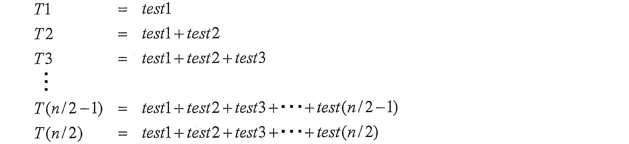
図18は、テスト信号testおよび反転テスト信号testBを生成するためのテスト信号生成回路53を示す図である。テスト信号生成回路53は、図4に示すテスト信号生成回路51において、シフトレジスタ301およびNORゲートNOR1を、それぞれシフトレジスタ302およびNORゲートNOR2に置き換えた構成である。
図19は、駆動回路220における動作確認テスト時のリセット信号RESET、信号TESTSP、信号TESTCKおよびテスト信号test1~test(n/2)の波形を示す図である。動作確認テストは、信号TESTSPを「H」レベルとすることにより開始される。信号TESTCKの立ち上がりにより、信号TESTSPが「H」レベルであることが、フリップフロップDFF0に認識される。これにより、シフトレジスタ302の各フリップフロップDFF0~DFF(n/2)は、信号TESTCKの立ち上がりに同期したパルス信号を、テスト信号test0~test(n/2)および反転テスト信号testB0~testB(n/2)として順次出力する。
本発明の第4の実施形態について、図21および図22を参照して以下に説明する。本実施形態では、第1の実施形態に係る表示装置90のさらに他の変形例である表示装置390について説明する。
まず、図21を参照して、本実施形態の表示装置390の概略構成を説明する。図21は、表示装置390の概略構成を示すブロック図である。表示装置390は、表示パネル80と駆動回路320とを備えている。駆動回路320は、図16に示す駆動回路220において、切替回路260および261を、それぞれ切替回路360および361に置き換えた構成である。
図22を参照して、本実施形態の駆動回路320の構成について説明する。図22は、駆動回路320の概略構成を示すブロック図である。
通常動作時は、第3の実施形態における通常動作と同様、テスト信号test0~test(n/2)は、すべて「L」レベルであり、反転テスト信号testB0~testB(n/2)はすべて「H」レベルである。したがって、サンプリング回路6-1~6-nは、それぞれホールド回路7-1~7-nに接続され、予備のホールド回路7-C、7-Dは、どのサンプリング回路6とも接続されない。
動作確認テストは、図18に示すテスト信号生成回路53において、信号TESTSPを「H」レベルとすることにより開始される。これにより、図19に示すように、テスト信号test0~test(n/2)が順次「H」レベルとなる。
本発明の第5の実施形態について、図23~図27を参照して以下に説明する。本実施形態では、第1の実施形態に係る表示装置90のさらに他の変形例である表示装置490について説明する。
図23を参照して、本実施形態に係る表示装置490の概略構成を説明する。図23は、表示装置490の概略構成を示すブロック図である。表示装置490は、表示パネル80と駆動回路420とを備えている。駆動回路420は、図2に示す駆動回路20において、切替回路61を切替回路461に置き換えた構成である。
図24を参照して、本実施形態に係る駆動回路420の構成について説明する。図24は、駆動回路420の概略構成を示すブロック図である。


図25は、駆動回路420における動作確認テスト時の、サンプリング信号STR1~STR3、サンプルリング回路6-1~6-3からの出力、信号LS、ホールド回路7-1~7-3からの出力、および出力端子OUTからの出力の波形を示す図である。サンプリング信号STR1~STR3は、図示しないポインター用シフトレジスタにより作成されるパルス信号であり、それぞれサンプルリング回路6-1~6-3のゲートに入力されて、サンプルリング回路6-1~6-3の動作を制御する。図25では、サンプリング信号は、サンプリング信号STR3までしか示されていないが、駆動回路420では、サンプリング信号STR1~STRnがそれぞれサンプリング回路6-1~6-nのゲートに入力される。なお、参照用サンプリング回路6-Aのゲートには、動作確認テスト用のサンプリング信号である信号TSTR1が入力される。
動作確認テストでは、データバスに、通常表示用の階調データの他、参照用階調データとテスト用階調データとを供給する。通常表示用の階調データ、参照用階調データおよびテスト用階調データを供給するタイミングについて、図26および図27に基づいて説明する。
信号LSが最初に立ち上がるタイミングTim1では、図24に示す駆動回路420は、以下の(1)~(4)のように動作する。
(1)信号LSが「H」レベルとなり、サンプリング回路6に保持された階調データがホールド回路7に転送される。
(2)テスト信号testA1が「H」レベルとなり、数3より、ゲート信号TA1~TAnが「L」レベルから「H」レベルに切り替わる。これにより、スイッチSWA1~SWAnでは、端子0と端子2とが接続され、サンプリング信号STRi(i=1~n-1)はサンプリング回路6-(i+1)に入力され、サンプリング信号STRnは、予備のサンプリング回路6-Bに入力される。
(3)データバスには通常駆動用の階調データに代わり、自己検出に使用する参照用階調データが供給される。
(4)参照用サンプリング回路6-Aのゲートに入力される信号TSTR1を「H」レベルにすることにより、参照用サンプリング回路6-Aがデータバスから参照用階調データを取り込む。参照用ホールド回路7-Aに入力される信号LSは「H」レベルであるので、同時に参照用階調データは参照用サンプリング回路6-Aから参照用ホールド回路7-Aに入力され、参照用ホールド回路7-Aは参照用階調データを保持する。
続いて、信号LSが立ち下がるタイミングTim2では、ホールド回路7とDAC回路8との接続は変更されないので、ホールド回路7-1に保持されている階調データは、DAC回路8-1によって階調電圧に変換されて、出力端子OUT1から出力される。つまり、出力端子OUT1から出力される階調電圧は、タイミングTim1より前におけるサンプリング回路6-1と出力端子OUT1との接続関係を保持した状態で出力端子OUT1から出力される階調電圧と同一である。同様に出力端子OUT2~OUTnからの階調電圧は、タイミングTim1より前におけるサンプリング回路6-2~6-nと出力端子OUT2~nとの接続関係を保持した状態で出力端子OUT2~nから出力される階調電圧とそれぞれ同一である。
次に信号LSが立ち上がるタイミングTim3において、駆動回路420は、以下の(1)~(6)のように動作する。
(1)信号LSが「H」レベルとなり、サンプリング回路6に保持された階調データがホールド回路7に転送される。
(2)テスト信号test1が「H」レベルとなり、数4より、ゲート信号TB1~TBnが「L」レベルから「H」レベルに切り替わる。これにより、スイッチSWB1~SWBnでは、端子0と端子2とが接続され、出力端子OUTi(i=1~n-1)はオペアンプ1-(i+1)に入力され、出力端子OUTnは、予備のオペアンプ1-Bに入力される。これにより、サンプリング回路6-1、ホールド回路7-1、DAC回路8-1およびオペアンプ1-1は、表示パネル80の駆動とは無関係になる。
(3)データバスには通常駆動用の階調データに代わり、自己検出に使用するテスト用階調データが供給される。
(4)信号TSTR2が「H」レベルとなり、テスト信号testA1が「H」レベルであることから、信号TSTR2がサンプリング回路6-1のゲートに入力される。これにより、サンプリング回路6-1は、データバスからテスト用階調データを取り込む。また、ホールド回路7-1に入力される信号LSは「H」レベルであるので、同時にテスト用階調データはサンプリング回路6-1からホールド回路7-1に入力され、ホールド回路7-1はテスト用階調データを保持する。
(5)テスト信号test1が「H」レベルであり、反転テスト信号testB1が「L」レベルであるので、オペアンプ1-1はコンパレータとして機能する。ここで、これにより、DAC回路8-1からはテスト用出力信号がオペアンプ1-1の正極性入力端子に入力され、参照用DAC回路8-Aからは参照出力信号がオペアンプ1-1の負極性入力端子に入力される。
(6)オペアンプ1-1からの出力は、判定回路3-1に入力され、判定回路3-1では、自身が記憶した期待値と、オペアンプ1-1からの出力とを比較する。当該期待値は、参照用階調データおよびテスト用階調データに基づき設定できる。これにより、1列目の出力回路の不具合を検出する。
データバスにはテスト用階調データに代わり、通常駆動用の階調データが供給される。なお、駆動回路420は、タイミングTim3における接続状態で、表示パネルへ階調電圧の出力を継続する。
さらに次に信号LSが立ち上がるタイミングTim5では、通常駆動用の階調データに代わり、データバスに参照用階調データが供給される。また、参照用サンプリング回路6-Aのゲートに入力される信号TSTR1が再び「H」レベルとなり、参照用サンプリング回路6-A、参照用ホールド回路7-Aに参照用階調データが保持される。
タイミングTim5の次に信号LSが立ち下がるタイミングTim6では、データバスには参照用階調データに代わり、通常駆動用の階調データが供給される。駆動回路420は、タイミングTim3における接続状態で、表示パネルへ階調電圧の出力を継続する。
タイミングTim6の次に信号LSが立ち上がるタイミングTim7では、データバスには通常駆動用の階調データに代わり、テスト用階調データが供給される。同時に、信号TSTR2を「H」レベルにして、サンプリング回路6-1およびホールド回路7-1にテスト用階調データを保持させる。これにより、タイミングTim3と同様に、参照用ホールド回路7-Aには、参照用階調データが保持され、ホールド回路7-1には、テスト用階調データが保持されている状態となる。オペアンプ1-1はコンパレータとして機能し、タイミングTim3と同様に、1列目の出力回路の不具合の検出を行う。
上記の実施形態1および2では、通常の出力回路、予備の出力回路、および参照用出力回路を設け、各出力回路の比較と表示パネルの駆動とを同時に行い、表示パネルを駆動する出力回路の切り替えは、DAC回路とホールド回路との接続、およびオペアンプと出力端子との接続を切り替えることで行っている。また、実施形態3および4では、通常の出力回路および予備の出力回路を設け、各出力回路の比較と表示パネルの駆動とを同時に行い、表示パネルを駆動する出力回路の切り替えは、サンプリング回路とホールド回路との接続、およびオペアンプと出力端子との接続を切り替えることで行っている。また、実施形態5では、通常の出力回路、予備の出力回路、および参照用出力回路を設け、各出力回路の比較と表示パネルの駆動とを同時に行い、表示パネルを駆動する出力回路の切り替えは、データバスとサンプリング回路との接続、およびを切り替え、およびオペアンプと出力端子との接続を切り替えることで行っている。
3-1~3-n、3-C、3-D 判定回路(判定手段)
6-1~6-n、6-A、6-B サンプリング回路
7-1~7-n、7-A~7-D ホールド回路
8-1~8-n、8-A~8-D DAC回路(デジタルアナログコンバータ)
10 ソースドライバ(駆動回路)
20、120、220、320、420 駆動回路
30 出力回路ブロック(第1の出力回路)
40 予備出力回路ブロック(第2の出力回路)
41 参照出力回路ブロック(第3の出力回路)
50 比較判定回路(比較手段、判定手段、自己検出・自己修復手段)
60、160、260、360 切替回路(切替手段、自己検出・自己修復手段)
61、161、261、361、461 切替回路(制御手段、自己検出・自己修復手 段)
80 表示パネル
90,190、290、390、490 表示装置
SWA1~SWAn スイッチ(制御回路)
SWB1~SWBn スイッチ(切替回路)
TDATA テスト用データバス(データバス)
Claims (23)
- 表示装置に映像信号を出力するn個(nは2以上の自然数)の出力端子と、自身の不良を検出し修復する手段を有する駆動回路であって、
入力データを映像信号に変換するとともに、上記出力端子に切り離し可能に接続された、n個の第1の出力回路と、
入力データを映像信号に変換するとともに、上記出力端子に切り離し可能に接続された、p個以上(pは1以上n以下の自然数)の第2の出力回路と、
上記出力端子に接続されず、入力データを映像信号に変換する第3の出力回路と、
上記第1の出力回路からp個の出力回路を選択し、上記出力端子との接続を切り離すとともに、上記第2の出力回路からp個の出力回路を上記出力端子に接続する切替手段と、
選択された第1の出力回路からの映像信号と、上記第3の出力回路からの映像信号とを比較する比較手段と、
当該比較手段の比較結果に基づき、上記選択された第1の出力回路が不良か否かを判定する判定手段とを備えることを特徴とする駆動回路。 - 上記切替手段は、
q番目からq+p-1番目(q+p-1はn以下の自然数)の上記第1の出力回路が選択された場合、r番目(rはq未満の自然数)の上記出力端子にr番目の上記第1の出力回路を接続すると共に、s番目(sはq以上n-p以下の自然数)の上記出力端子に、s+p番目の上記第1の出力回路を接続し、t番目(tはn-pより大きくn以下の自然数)の上記出力端子に、上記第2の出力回路を接続することを特徴とする請求項1に記載の駆動回路。 - 上記切替手段は、上記選択された第1の出力回路が接続を切り離した出力端子と上記第2の出力回路とを接続することを特徴とする請求項1に記載の駆動回路。
- 上記入力データが供給されるデータバスを介して、上記第1~第3の出力回路に上記入力データを入力する制御手段を備え、
上記制御手段は、上記選択された第1の出力回路に入力される入力データと、上記第3の出力回路に入力される入力データとが異なる値の入力データとなるように制御することを特徴とする請求項1~3のいずれか1項に記載の駆動回路。 - 上記データバスは、第1~第3のデータバスから構成され、
上記制御手段は、
上記第1のデータバスを介して、上記選択された第1の出力回路を除く第1の出力回路と上記第2の出力回路とに上記入力データを入力し、
上記第2のデータバスを介して、上記選択された第1の出力回路に上記入力データを入力し、
上記第3のデータバスを介して、上記第3の出力回路に上記入力データを入力することを特徴とする請求項4に記載の駆動回路。 - 上記制御手段は、1つのデータバスを介して上記第1~第3の出力回路に上記入力データを入力することを特徴とする請求項4に記載の駆動回路。
- 上記映像信号が階調電圧であり、上記第1~第3の出力回路は、上記入力データを上記階調電圧に変換するデジタルアナログコンバータを備え、
上記比較手段は、上記選択された第1の出力回路に備えられるデジタルアナログコンバータからの階調電圧と、上記第3の出力回路に備えられるデジタルアナログコンバータからの階調電圧とを比較することを特徴とする請求項1~3のいずれか1項に記載の駆動回路。 - 上記第1の出力回路は、上記デジタルアナログコンバータの出力バッファーとしてオペアンプを備え、
上記オペアンプは、当該オペアンプを備える第1の出力回路が上記切替手段によって選択されて上記出力端子と接続されていないときに、コンパレータとして動作し、
上記比較手段は、上記コンパレータとして動作するオペアンプであることを特徴とする請求項7に記載の駆動回路。 - 上記第3の出力回路は、上記コンパレータとして動作するオペアンプに接続されることを特徴とする請求項8に記載の駆動回路。
- 上記オペアンプは、当該オペアンプを備える第1の出力回路が上記出力端子と接続されているときに、ボルテージフォロワとして動作することを特徴とする請求項8に記載の駆動回路。
- 上記判定手段は、上記選択された第1の出力回路および上記第3の出力回路にそれぞれ入力される入力データに対応する、上記比較手段からの比較結果を期待値として記憶しており、
上記比較結果と上記期待値とが異なる場合に、上記選択された第1の出力回路を不良であると判定することを特徴とする請求項1~3のいずれか1項に記載の駆動回路。 - 表示装置に映像信号を出力するn個(nは2以上の自然数)の出力端子と、自身の不良を検出し修復する手段を有する駆動回路であって、
入力データを映像信号に変換するとともに、上記出力端子に切り離し可能に接続された、n個の第1の出力回路と、
入力データを映像信号に変換するとともに、上記出力端子に切り離し可能に接続された、u個以上(uは2以上n以下の偶数)の第2の出力回路と、
上記第1の出力回路からu個の出力回路を選択し、上記出力端子との接続を切り離すとともに、上記第2の出力回路からu個の出力回路を上記出力端子に接続する切替手段と、
選択された第1の出力回路のうち任意の2つを第1の選択出力回路および第2の選択出力回路として、上記第1の選択出力回路からの映像信号と、上記第2の選択出力回路の映像信号とを比較する比較手段と、
当該比較手段の比較結果に基づき、上記選択された第1の出力回路が不良か否かを判定する判定手段とを備えることを特徴とする駆動回路。 - 上記切替手段は、
v番目からv+u-1番目(v+u-1はn以下の自然数)の上記出力回路が選択された場合、w番目(wはv未満の自然数)の上記出力端子にw番目の上記第1の出力回路を接続すると共に、x番目(xはv以上n-u以下の自然数)の上記出力端子に、x+u番目の上記第1の出力回路を接続し、y番目(yはn-uより大きくn以下の自然数)の上記出力端子に、上記第2の出力回路を接続することを特徴とする請求項12に記載の駆動回路。 - 上記切替手段は、上記選択された第1の出力回路が接続を切り離した出力端子と上記第2の出力回路とを接続することを特徴とする請求項12に記載の駆動回路。
- 上記第1および第2の出力回路に上記入力データを入力する制御手段を備え、
上記制御手段は、上記第1の選択出力回路に入力される入力データと、上記第2の選択出力回路に入力される入力データとが異なる値の入力データとなるように制御することを特徴とする請求項12~14のいずれか1項に記載の駆動回路。 - 上記映像信号が階調電圧であり、上記第1の出力回路は、上記入力データを上記階調電圧に変換するデジタルアナログコンバータを備え、
上記比較手段は、上記第1の選択出力回路に備えられるデジタルアナログコンバータからの階調電圧と、上記第2の選択出力回路に備えられるデジタルアナログコンバータからの階調電圧とを比較することを特徴とする請求項12~14のいずれか1項に記載の駆動回路。 - 上記第1の出力回路は、上記デジタルアナログコンバータの出力バッファーとしてオペアンプを備え、
上記オペアンプは、当該オペアンプを備える第1の出力回路が上記切替手段によって選択されて上記出力端子と接続されていないときに、コンパレータとして動作し、
上記比較手段は、上記コンパレータとして動作するオペアンプであることを特徴とする請求項16に記載の駆動回路。 - 上記オペアンプは、当該オペアンプを備える第1の出力回路が上記出力端子と接続されているときに、ボルテージフォロワとして動作することを特徴とする請求項17に記載の駆動回路。
- 上記判定手段は、上記第1の選択出力回路と上記第2の選択出力回路とに入力される入力データに対応する、上記比較手段からの比較結果を期待値として記憶しており、
上記比較結果と上記期待値とが異なる場合に、上記選択された第1の出力回路を不良であると判定することを特徴とする請求項12~14のいずれか1項に記載の駆動回路。 - 上記第1および第2の出力回路に上記入力データを入力する制御手段を備え、
上記制御手段は、上記第1の選択出力回路に入力される入力データと、上記第2の選択出力回路に入力される入力データとが異なる値の入力データとなるように制御し、
上記第1の出力回路は、
上記入力データを時分割で取り込んで保持するサンプリング回路と、
上記サンプリング回路に保持された入力データを時分割で取り込んで上記デジタルアナログコンバータに出力するホールド回路とを備え、
上記制御手段は、
通常駆動時に、上記サンプリング回路に上記入力データを入力し、
自己検出時に、上記選択された第1の出力回路のデジタルアナログコンバータに上記入力データを入力することを特徴とする請求項16に記載の駆動回路。 - 請求項1~3、12~14のいずれか1項に記載の駆動回路を備えていることを特徴とする表示装置。
- 表示装置に映像信号を出力するn個(nは2以上の自然数)の出力端子と、
入力データを映像信号に変換するとともに、上記出力端子に切り離し可能に接続された、n個の第1の出力回路と、
入力データを映像信号に変換するとともに、上記出力端子に切り離し可能に接続された、p個以上(pは1以上n以下の自然数)の第2の出力回路と、
上記出力端子に接続されず、入力データを映像信号に変換する第3の出力回路とを備える駆動回路の不良を検出し修復する自己検出・自己修復方法であって、
上記第1の出力回路からp個の出力回路を選択して、選択された第1の出力回路と上記出力端子との接続を切り離すとともに、上記第2の出力回路からp個の出力回路を上記出力端子に接続する切替ステップと、
上記選択された第1の出力回路からの映像信号と、上記第3の出力回路からの映像信号とを比較する比較ステップと、
上記比較ステップの比較結果に基づき、上記選択された第1の出力回路が不良か否かを判定する判定ステップとを有することを特徴とする自己検出・自己修復方法。 - 表示装置に映像信号を出力するn個(nは2以上の自然数)の出力端子と、
入力データを映像信号に変換するとともに、上記出力端子に切り離し可能に接続された、n個の第1の出力回路と、
入力データを映像信号に変換するとともに、上記出力端子に切り離し可能に接続された、u個以上(uは2以上n以下の偶数)の第2の出力回路とを備える駆動回路の不良を検出し修復する自己検出・自己修復方法であって、
上記第1の出力回路からu個の出力回路を選択して、選択された第1の出力回路と上記出力端子との接続を切り離すとともに、上記第2の出力回路からu個の出力回路を上記出力端子に接続する切替ステップと、
上記選択された第1の出力回路のうち任意の2つを第1の選択出力回路および第2の選択出力回路として、上記選択された第1の選択出力回路からの映像信号と、上記第2の選択出力回路からの映像信号とを比較する比較ステップと、
上記比較ステップの比較結果に基づき、上記選択された第1の出力回路が不良か否かを判定する判定ステップとを有することを特徴とする自己検出・自己修復方法。
Priority Applications (3)
| Application Number | Priority Date | Filing Date | Title |
|---|---|---|---|
| US13/131,419 US20110254822A1 (en) | 2008-11-28 | 2009-11-25 | Drive circuit, display device and method for self-detecting and self-repairing drive circuit |
| KR1020117014516A KR101247904B1 (ko) | 2008-11-28 | 2009-11-25 | 구동 회로, 표시 장치 및 구동 회로의 자기 검출ㆍ자기 수복 방법 |
| CN200980147209.8A CN102227764B (zh) | 2008-11-28 | 2009-11-25 | 驱动电路、显示装置以及驱动电路的自检测/自修复方法 |
Applications Claiming Priority (2)
| Application Number | Priority Date | Filing Date | Title |
|---|---|---|---|
| JP2008304735A JP5154386B2 (ja) | 2008-11-28 | 2008-11-28 | 駆動回路および表示装置 |
| JP2008-304735 | 2008-11-28 |
Publications (1)
| Publication Number | Publication Date |
|---|---|
| WO2010061839A1 true WO2010061839A1 (ja) | 2010-06-03 |
Family
ID=42225712
Family Applications (1)
| Application Number | Title | Priority Date | Filing Date |
|---|---|---|---|
| PCT/JP2009/069839 WO2010061839A1 (ja) | 2008-11-28 | 2009-11-25 | 駆動回路、表示装置および駆動回路の自己検出・自己修復方法 |
Country Status (6)
| Country | Link |
|---|---|
| US (1) | US20110254822A1 (ja) |
| JP (1) | JP5154386B2 (ja) |
| KR (1) | KR101247904B1 (ja) |
| CN (1) | CN102227764B (ja) |
| TW (1) | TWI424402B (ja) |
| WO (1) | WO2010061839A1 (ja) |
Families Citing this family (16)
| Publication number | Priority date | Publication date | Assignee | Title |
|---|---|---|---|---|
| KR101133486B1 (ko) * | 2008-02-28 | 2012-07-12 | 샤프 가부시키가이샤 | 구동 회로 및 표시 장치 |
| US8810268B2 (en) * | 2010-04-21 | 2014-08-19 | Taiwan Semiconductor Manufacturing Company, Ltd. | Built-in self-test circuit for liquid crystal display source driver |
| EP2801022A1 (en) | 2012-01-05 | 2014-11-12 | American Panel Corporation Inc. | Redundant control system for lcd |
| TWI463471B (zh) * | 2012-08-13 | 2014-12-01 | Novatek Microelectronics Corp | 液晶顯示面板的驅動裝置 |
| CN104284210A (zh) * | 2013-07-05 | 2015-01-14 | 上海帕科软件科技有限公司 | Iptv故障自诊断网络系统 |
| CN103745700B (zh) * | 2013-12-27 | 2015-10-07 | 深圳市华星光电技术有限公司 | 自修复型栅极驱动电路 |
| JP6027570B2 (ja) * | 2014-03-27 | 2016-11-16 | 大陽日酸株式会社 | 冗長化システム、故障検出装置、冗長化方法 |
| JP6706954B2 (ja) * | 2016-04-01 | 2020-06-10 | 三菱電機株式会社 | ドライバicおよび液晶表示装置 |
| CN105976785B (zh) * | 2016-07-21 | 2018-12-28 | 武汉华星光电技术有限公司 | Goa电路及液晶显示面板 |
| US11011096B2 (en) * | 2016-08-25 | 2021-05-18 | Sharp Nec Display Solutions, Ltd. | Self-diagnostic imaging method, self-diagnostic imaging program, display device, and self-diagnostic imaging system |
| EP3580744A1 (en) | 2017-02-09 | 2019-12-18 | L-3 Technologies, Inc. | Fault-tolerant liquid crystal displays for avionics systems |
| US20200013321A1 (en) * | 2018-07-09 | 2020-01-09 | Sharp Kabushiki Kaisha | Display device and method for detecting state thereof |
| JP7065409B2 (ja) * | 2018-09-25 | 2022-05-12 | パナソニックIpマネジメント株式会社 | 処理システム、センサシステム、移動体、異常判定方法、及びプログラム |
| CN110415632B (zh) * | 2019-07-23 | 2023-01-17 | 安徽天域视听器材有限公司 | 基于语音控制的视频传输系统及其传输方法 |
| US11783739B2 (en) * | 2020-09-10 | 2023-10-10 | Apple Inc. | On-chip testing architecture for display system |
| TWI780869B (zh) * | 2021-08-23 | 2022-10-11 | 大陸商集創北方(珠海)科技有限公司 | 具自我偵錯功能之顯示驅動晶片、顯示裝置及資訊處理裝置 |
Citations (3)
| Publication number | Priority date | Publication date | Assignee | Title |
|---|---|---|---|---|
| JPH10339861A (ja) * | 1997-03-15 | 1998-12-22 | Sharp Corp | フォールトトレラントアーキテクチャ |
| JP2002043943A (ja) * | 2000-07-21 | 2002-02-08 | Toshiba Corp | アナログ出力装置 |
| JP2008139861A (ja) * | 2006-11-10 | 2008-06-19 | Toshiba Matsushita Display Technology Co Ltd | 有機発光素子を用いたアクティブマトリクス型表示装置、および有機発光素子を用いたアクティブマトリクス型表示装置の駆動方法 |
Family Cites Families (12)
| Publication number | Priority date | Publication date | Assignee | Title |
|---|---|---|---|---|
| US4853901A (en) * | 1986-02-18 | 1989-08-01 | Diagnostic Services, Inc. | Automatic liquid level recording device |
| JPH11272224A (ja) * | 1998-03-24 | 1999-10-08 | Toshiba Corp | 表示装置の駆動回路 |
| US7187805B1 (en) * | 1999-11-23 | 2007-03-06 | Xerox Corporation | Maximum likelihood estimation of JPEG quantization values |
| US6816143B1 (en) * | 1999-11-23 | 2004-11-09 | Koninklijke Philips Electronics N.V. | Self diagnostic and repair in matrix display panel |
| JP4564146B2 (ja) * | 2000-08-31 | 2010-10-20 | シャープ株式会社 | 液晶駆動回路及びそれを用いた液晶表示装置 |
| JP4068040B2 (ja) * | 2003-10-10 | 2008-03-26 | 富士通株式会社 | オペアンプ、ラインドライバおよび液晶表示装置 |
| TWI278647B (en) * | 2003-11-07 | 2007-04-11 | Renesas Tech Corp | Semiconductor device and testing method thereof |
| JP3969387B2 (ja) * | 2003-12-05 | 2007-09-05 | 松下電器産業株式会社 | 映像信号出力装置 |
| JP5179775B2 (ja) * | 2007-04-19 | 2013-04-10 | ラピスセミコンダクタ株式会社 | オフセットキャンセル装置、icチップ、及び駆動ic |
| JP4277055B2 (ja) * | 2007-05-29 | 2009-06-10 | シャープ株式会社 | 駆動回路、表示装置、およびテレビジョンシステム |
| JP2009008943A (ja) * | 2007-06-28 | 2009-01-15 | Sony Corp | 表示装置 |
| KR101133486B1 (ko) * | 2008-02-28 | 2012-07-12 | 샤프 가부시키가이샤 | 구동 회로 및 표시 장치 |
-
2008
- 2008-11-28 JP JP2008304735A patent/JP5154386B2/ja active Active
-
2009
- 2009-11-25 US US13/131,419 patent/US20110254822A1/en not_active Abandoned
- 2009-11-25 CN CN200980147209.8A patent/CN102227764B/zh active Active
- 2009-11-25 WO PCT/JP2009/069839 patent/WO2010061839A1/ja active Application Filing
- 2009-11-25 KR KR1020117014516A patent/KR101247904B1/ko active IP Right Grant
- 2009-11-26 TW TW098140407A patent/TWI424402B/zh active
Patent Citations (3)
| Publication number | Priority date | Publication date | Assignee | Title |
|---|---|---|---|---|
| JPH10339861A (ja) * | 1997-03-15 | 1998-12-22 | Sharp Corp | フォールトトレラントアーキテクチャ |
| JP2002043943A (ja) * | 2000-07-21 | 2002-02-08 | Toshiba Corp | アナログ出力装置 |
| JP2008139861A (ja) * | 2006-11-10 | 2008-06-19 | Toshiba Matsushita Display Technology Co Ltd | 有機発光素子を用いたアクティブマトリクス型表示装置、および有機発光素子を用いたアクティブマトリクス型表示装置の駆動方法 |
Also Published As
| Publication number | Publication date |
|---|---|
| JP2010128324A (ja) | 2010-06-10 |
| US20110254822A1 (en) | 2011-10-20 |
| KR20110089434A (ko) | 2011-08-08 |
| CN102227764A (zh) | 2011-10-26 |
| TW201037659A (en) | 2010-10-16 |
| JP5154386B2 (ja) | 2013-02-27 |
| KR101247904B1 (ko) | 2013-03-26 |
| CN102227764B (zh) | 2014-04-16 |
| TWI424402B (zh) | 2014-01-21 |
Similar Documents
| Publication | Publication Date | Title |
|---|---|---|
| JP5154386B2 (ja) | 駆動回路および表示装置 | |
| JP4277055B2 (ja) | 駆動回路、表示装置、およびテレビジョンシステム | |
| CN102144253B (zh) | 显示装置及其驱动方法 | |
| US6191770B1 (en) | Apparatus and method for testing driving circuit in liquid crystal display | |
| US8068080B2 (en) | Display apparatus, source driver, and display panel driving method | |
| US8026889B2 (en) | Drive circuit of display device and method of testing the same | |
| JP2009015247A (ja) | 表示装置のデータドライバ、そのテスト方法及びプローブカード | |
| US20050083278A1 (en) | Driving circuit of display device and method of driving same | |
| WO2017150175A1 (ja) | 表示装置及び表示装置の検査方法 | |
| WO2009107469A1 (ja) | 駆動回路および表示装置 | |
| WO2010035797A1 (ja) | 表示装置、およびテレビジョンシステム | |
| JP2018004887A (ja) | 表示制御デバイス及び表示パネルモジュール | |
| US9164301B2 (en) | Display device | |
| JP4094328B2 (ja) | 表示装置駆動回路および表示装置駆動回路の駆動方法 | |
| WO2010058836A1 (ja) | 表示装置、およびテレビジョンシステム | |
| US20060181526A1 (en) | Display driver | |
| WO2010035792A1 (ja) | 表示装置、およびテレビジョンシステム | |
| WO2010035785A1 (ja) | 表示装置、およびテレビジョンシステム | |
| JP5015038B2 (ja) | 駆動回路および該駆動回路を備えた表示装置 | |
| JP5015041B2 (ja) | 駆動回路および駆動回路を備えた表示装置 | |
| JP5015037B2 (ja) | 駆動回路および該駆動回路を備えた表示装置 | |
| CN114554121A (zh) | 显示装置以及显示装置的控制方法 | |
| KR20080078475A (ko) | 액정표시장치의 테스트 회로 | |
| KR20080003199A (ko) | 화상표시장치 및 이의 구동방법 | |
| JPH07199876A (ja) | シフトレジスタ及びアクティブマトリクス方式tft−lcd並びに駆動回路の駆動方法 |
Legal Events
| Date | Code | Title | Description |
|---|---|---|---|
| WWE | Wipo information: entry into national phase |
Ref document number: 200980147209.8 Country of ref document: CN |
|
| 121 | Ep: the epo has been informed by wipo that ep was designated in this application |
Ref document number: 09829087 Country of ref document: EP Kind code of ref document: A1 |
|
| WWE | Wipo information: entry into national phase |
Ref document number: 13131419 Country of ref document: US |
|
| NENP | Non-entry into the national phase |
Ref country code: DE |
|
| ENP | Entry into the national phase |
Ref document number: 20117014516 Country of ref document: KR Kind code of ref document: A |
|
| 122 | Ep: pct application non-entry in european phase |
Ref document number: 09829087 Country of ref document: EP Kind code of ref document: A1 |