WO2010061696A1 - 導電部材及びこれを用いた固体高分子形燃料電池 - Google Patents
導電部材及びこれを用いた固体高分子形燃料電池 Download PDFInfo
- Publication number
- WO2010061696A1 WO2010061696A1 PCT/JP2009/068048 JP2009068048W WO2010061696A1 WO 2010061696 A1 WO2010061696 A1 WO 2010061696A1 JP 2009068048 W JP2009068048 W JP 2009068048W WO 2010061696 A1 WO2010061696 A1 WO 2010061696A1
- Authority
- WO
- WIPO (PCT)
- Prior art keywords
- layer
- conductive
- intermediate layer
- conductive carbon
- metal
- Prior art date
Links
Images


Classifications
-
- H—ELECTRICITY
- H01—ELECTRIC ELEMENTS
- H01B—CABLES; CONDUCTORS; INSULATORS; SELECTION OF MATERIALS FOR THEIR CONDUCTIVE, INSULATING OR DIELECTRIC PROPERTIES
- H01B5/00—Non-insulated conductors or conductive bodies characterised by their form
- H01B5/02—Single bars, rods, wires, or strips
-
- H—ELECTRICITY
- H01—ELECTRIC ELEMENTS
- H01M—PROCESSES OR MEANS, e.g. BATTERIES, FOR THE DIRECT CONVERSION OF CHEMICAL ENERGY INTO ELECTRICAL ENERGY
- H01M8/00—Fuel cells; Manufacture thereof
- H01M8/02—Details
- H01M8/0202—Collectors; Separators, e.g. bipolar separators; Interconnectors
- H01M8/0204—Non-porous and characterised by the material
- H01M8/0213—Gas-impermeable carbon-containing materials
-
- H—ELECTRICITY
- H01—ELECTRIC ELEMENTS
- H01B—CABLES; CONDUCTORS; INSULATORS; SELECTION OF MATERIALS FOR THEIR CONDUCTIVE, INSULATING OR DIELECTRIC PROPERTIES
- H01B13/00—Apparatus or processes specially adapted for manufacturing conductors or cables
-
- H—ELECTRICITY
- H01—ELECTRIC ELEMENTS
- H01M—PROCESSES OR MEANS, e.g. BATTERIES, FOR THE DIRECT CONVERSION OF CHEMICAL ENERGY INTO ELECTRICAL ENERGY
- H01M8/00—Fuel cells; Manufacture thereof
- H01M8/02—Details
-
- H—ELECTRICITY
- H01—ELECTRIC ELEMENTS
- H01M—PROCESSES OR MEANS, e.g. BATTERIES, FOR THE DIRECT CONVERSION OF CHEMICAL ENERGY INTO ELECTRICAL ENERGY
- H01M8/00—Fuel cells; Manufacture thereof
- H01M8/02—Details
- H01M8/0202—Collectors; Separators, e.g. bipolar separators; Interconnectors
- H01M8/0204—Non-porous and characterised by the material
- H01M8/0223—Composites
- H01M8/0228—Composites in the form of layered or coated products
-
- H—ELECTRICITY
- H01—ELECTRIC ELEMENTS
- H01M—PROCESSES OR MEANS, e.g. BATTERIES, FOR THE DIRECT CONVERSION OF CHEMICAL ENERGY INTO ELECTRICAL ENERGY
- H01M8/00—Fuel cells; Manufacture thereof
- H01M8/10—Fuel cells with solid electrolytes
-
- H—ELECTRICITY
- H01—ELECTRIC ELEMENTS
- H01M—PROCESSES OR MEANS, e.g. BATTERIES, FOR THE DIRECT CONVERSION OF CHEMICAL ENERGY INTO ELECTRICAL ENERGY
- H01M8/00—Fuel cells; Manufacture thereof
- H01M8/10—Fuel cells with solid electrolytes
- H01M2008/1095—Fuel cells with polymeric electrolytes
-
- H—ELECTRICITY
- H01—ELECTRIC ELEMENTS
- H01M—PROCESSES OR MEANS, e.g. BATTERIES, FOR THE DIRECT CONVERSION OF CHEMICAL ENERGY INTO ELECTRICAL ENERGY
- H01M8/00—Fuel cells; Manufacture thereof
- H01M8/10—Fuel cells with solid electrolytes
- H01M8/12—Fuel cells with solid electrolytes operating at high temperature, e.g. with stabilised ZrO2 electrolyte
- H01M2008/1293—Fuel cells with solid oxide electrolytes
-
- H—ELECTRICITY
- H01—ELECTRIC ELEMENTS
- H01M—PROCESSES OR MEANS, e.g. BATTERIES, FOR THE DIRECT CONVERSION OF CHEMICAL ENERGY INTO ELECTRICAL ENERGY
- H01M8/00—Fuel cells; Manufacture thereof
- H01M8/14—Fuel cells with fused electrolytes
- H01M2008/147—Fuel cells with molten carbonates
-
- H—ELECTRICITY
- H01—ELECTRIC ELEMENTS
- H01M—PROCESSES OR MEANS, e.g. BATTERIES, FOR THE DIRECT CONVERSION OF CHEMICAL ENERGY INTO ELECTRICAL ENERGY
- H01M8/00—Fuel cells; Manufacture thereof
- H01M8/02—Details
- H01M8/0202—Collectors; Separators, e.g. bipolar separators; Interconnectors
- H01M8/0247—Collectors; Separators, e.g. bipolar separators; Interconnectors characterised by the form
- H01M8/0254—Collectors; Separators, e.g. bipolar separators; Interconnectors characterised by the form corrugated or undulated
-
- H—ELECTRICITY
- H01—ELECTRIC ELEMENTS
- H01M—PROCESSES OR MEANS, e.g. BATTERIES, FOR THE DIRECT CONVERSION OF CHEMICAL ENERGY INTO ELECTRICAL ENERGY
- H01M8/00—Fuel cells; Manufacture thereof
- H01M8/08—Fuel cells with aqueous electrolytes
- H01M8/083—Alkaline fuel cells
-
- H—ELECTRICITY
- H01—ELECTRIC ELEMENTS
- H01M—PROCESSES OR MEANS, e.g. BATTERIES, FOR THE DIRECT CONVERSION OF CHEMICAL ENERGY INTO ELECTRICAL ENERGY
- H01M8/00—Fuel cells; Manufacture thereof
- H01M8/08—Fuel cells with aqueous electrolytes
- H01M8/086—Phosphoric acid fuel cells [PAFC]
-
- Y—GENERAL TAGGING OF NEW TECHNOLOGICAL DEVELOPMENTS; GENERAL TAGGING OF CROSS-SECTIONAL TECHNOLOGIES SPANNING OVER SEVERAL SECTIONS OF THE IPC; TECHNICAL SUBJECTS COVERED BY FORMER USPC CROSS-REFERENCE ART COLLECTIONS [XRACs] AND DIGESTS
- Y02—TECHNOLOGIES OR APPLICATIONS FOR MITIGATION OR ADAPTATION AGAINST CLIMATE CHANGE
- Y02E—REDUCTION OF GREENHOUSE GAS [GHG] EMISSIONS, RELATED TO ENERGY GENERATION, TRANSMISSION OR DISTRIBUTION
- Y02E60/00—Enabling technologies; Technologies with a potential or indirect contribution to GHG emissions mitigation
- Y02E60/30—Hydrogen technology
- Y02E60/50—Fuel cells
Definitions
- the present invention relates to a conductive member and a polymer electrolyte fuel cell using the same.
- the polymer electrolyte fuel cell has a structure in which a plurality of single cells exhibiting a power generation function are stacked.
- Each of the single cells includes (1) a polymer electrolyte membrane, (2) a pair of catalyst layers sandwiching the polymer electrolyte membrane, and (3) a pair of gas diffusion layers (GDL) for sandwiching them and dispersing the supply gas.
- GDL gas diffusion layers
- MEA membrane electrode assembly
- MEA which each single cell has is electrically connected with MEA of an adjacent single cell through a separator.
- a fuel cell stack is comprised by laminating
- the fuel cell stack functions as power generation means that can be used for various applications.
- the separator exhibits a function of electrically connecting adjacent single cells as described above.
- a gas flow path is usually provided on the surface of the separator facing the MEA.
- the gas flow path functions as a gas supply means for supplying fuel gas and oxidant gas to the anode and the cathode, respectively.
- metals, carbon, conductive resins, and the like are known as constituent materials for fuel cell separators that require electrical conductivity.
- the carbon separator and the conductive resin separator it is necessary to set the thickness relatively large in order to secure the strength after forming the gas flow path to some extent.
- the overall thickness of the fuel cell stack using these separators also increases.
- the increase in the size of the stack is not preferable especially in an in-vehicle PEFC that requires a reduction in size.
- the metal separator since the metal separator has a relatively high strength, the thickness can be made relatively small. Moreover, since it is excellent also in electroconductivity, when a metal separator is used, there also exists an advantage that contact resistance with MEA is reduced. On the other hand, metal materials may have problems such as a decrease in conductivity due to corrosion and a decrease in stack output. Therefore, the metal separator is required to improve the corrosion resistance while ensuring its excellent conductivity.
- Patent Document 1 a metal layer such as Ti or a carbide layer thereof is formed on one surface of a metal substrate of a metal separator, and is composed of graphitized carbon on the metal layer or the carbide layer.
- a technique for forming a carbon layer is disclosed.
- Patent Document 2 discloses a technique in which an oxide film of a base material is formed between a base material of a metal separator and a conductive thin film to form an intermediate layer made of a metal element or a metalloid element. .
- Patent Document 3 discloses a separator in which a carbon-based film containing a composite of metal oxide is formed on a substrate.
- the crystal structure of the carbon layer is various.
- the corrosion resistance and conductivity of the separator itself vary due to this.
- the oxide film disposed on the surface of the base material itself is a highly insulating layer. For this reason, the electrical conductivity in the thickness direction of the separator is lowered.
- the conductivity in the thickness direction of the separator is reduced or the contact resistance with the gas diffusion layer is increased. Resulting in.
- the present invention has been made in view of such problems of the conventional technology.
- the object of the present invention is to provide a conductive member having sufficiently improved corrosion resistance while sufficiently ensuring excellent conductivity in the conductive member, a manufacturing method thereof, and a polymer electrolyte fuel cell using the conductive member. It is in.
- the conductive member according to the first aspect of the present invention includes a base material, a conductive carbon layer that is located on at least one surface of the base material, and further includes conductive carbon, and the base material and the conductive carbon layer. And an intermediate layer interposed between the D band peak intensity (I D ) and G band peak intensity (I G ) measured by Raman scattering spectroscopy in the conductive carbon layer. And the intensity ratio R (I D / I G ) is 1.3 or more.
- the polymer electrolyte fuel cell according to the second aspect of the present invention includes the conductive member.
- FIG. 1 is a schematic cross-sectional view showing a basic configuration of a cell unit of a polymer electrolyte fuel cell using a conductive member (separator) in the first embodiment.
- FIG. 2 is a cross-sectional view schematically showing the configuration of the metal substrate of the separator of FIG. 1 and the treatment layer formed on the substrate.
- FIG. 3 is a schematic cross-sectional view showing the surface of the metal separator in FIG. 4A is a cross-sectional view schematically showing a configuration in which an intermediate layer and a conductive carbon layer are provided on both surfaces of a metal substrate in the separator of FIG.
- FIG. 4B is an enlarged view showing one embodiment of the intermediate layer and the conductive carbon layer.
- FIG. 1 is a schematic cross-sectional view showing a basic configuration of a cell unit of a polymer electrolyte fuel cell using a conductive member (separator) in the first embodiment.
- FIG. 2 is a cross-sectional view schematically showing the configuration
- FIG. 4C is an enlarged view showing another form of the intermediate layer and the conductive carbon layer.
- FIG. 6A is a schematic diagram showing a three-fold symmetry pattern of an average peak in the measurement of rotational anisotropy in Raman scattering spectroscopic analysis.
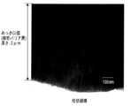
- FIG. 5B is a photograph (magnification: 400,000 times) of a cross
- FIG. 6B is a schematic diagram showing a two-fold symmetry pattern of an average peak in rotational anisotropy measurement of Raman scattering spectroscopic analysis.
- FIG. 6C is a schematic diagram showing a pattern that does not show the symmetry of the average peak in the measurement of rotational anisotropy of Raman scattering spectroscopic analysis.
- FIG. 7A is a graph showing a Raman spectrum when the conductive member B is used as a measurement sample, and the rotation angles of the sample are 0 °, 60 °, and 180 °, respectively.
- FIG. 7B is a graph showing the average peak of rotational anisotropy measurement for conductive member B.
- FIG. 8 shows the Vickers hardness of the conductive carbon layer and the sp 3 ratio of the conductive carbon layer in the conductive member in which the Vickers hardness of the conductive carbon layer is varied by changing the bias voltage and the film formation method by sputtering. It is a figure which shows the relationship with the value of.
- FIG. 9 is a graph showing the results of measurement of contact resistance for conductive members having conductive carbon layers having different R atom values but having different hydrogen atom contents.
- FIG. 10 is a conceptual diagram of a vehicle equipped with a fuel cell stack according to an embodiment of the present invention.
- FIG. 11 is a schematic diagram showing an outline of a measuring apparatus used for measuring contact resistance in Examples.
- FIG. 12A is a graph showing the results of measurement of contact resistance before and after the immersion test for the conductive members produced in Examples I-1 to I-7 and Comparative Examples I-1 to I-5.
- FIG. 12B is a graph showing the results of measurement of contact resistance before and after the immersion test for the conductive members produced in Example I-8 and Example I-9.
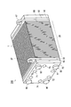
- FIG. 13 is a schematic view showing a fuel cell stack to which a conductive member according to an embodiment of the present invention is applied.
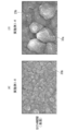
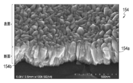
- 14 is a perspective view of the fuel cell stack of FIG. 15a and 15b are SEM photographs of the surfaces of Example I-9 and Example I-8. 16a and 16b are enlarged views of the SEM photographs of FIGS. 15a and 15b.
- FIG. 17a and 17b are TEM photographs of the cross sections of Example I-9 and Example I-8.
- 18a and 18b are SEM photographs observing the cross sections of Example I-9 and Example I-8.
- FIG. 19 is a schematic plan view showing a manufacturing apparatus for forming an intermediate layer and a conductive carbon layer by sputtering.
- FIG. 20 is a schematic plan view showing a manufacturing apparatus for forming an intermediate layer and a conductive carbon layer by an arc ion plating method.
- FIG. 21 is a schematic cross-sectional view showing the configuration of the surface of the conductive member (separator) in the second embodiment.
- FIG. 22A is a photograph showing the result of image analysis of the cross section of the dense barrier layer produced in Reference Example II-1 by TEM.
- FIG. 22B is a photograph showing the result of image analysis of the cross section of the intermediate layer produced in Reference Example II-2 by TEM.
- FIG. 23A is a photograph showing a result of image analysis of the surface of the dense barrier layer produced in Reference Example II-1 by SEM.
- FIG. 23B is a photograph showing the result of image analysis performed on the surface of the intermediate layer prepared in Reference Example II-2 by SEM.
- FIG. 23C is an SEM photograph showing the result of image analysis of the dense barrier layer produced in Reference Example II-1 in more detail than in FIG. 23A.
- FIG. 23D is a SEM photograph showing the result of image analysis of the intermediate layer produced in Reference Example II-2 in more detail than FIG. 23B.
- FIG. 23A is a photograph showing a result of image analysis of the surface of the dense barrier layer produced in Reference Example II-1 by SEM.
- FIG. 24 is a photograph showing the result of image analysis of the cross section of the conductive member produced in Example II-2 by TEM.
- FIG. 25 is a schematic cross-sectional view showing the configuration of the surface of the conductive member (separator) in the third embodiment.
- FIG. 26 is a graph showing the measurement results of element concentration by Auger electron spectroscopy of a metal substrate (SUS316L) immersed in an aqueous sulfuric acid solution at 80 ° C. and pH 4 for 100 hours.
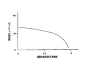
- FIG. 27 is a graph showing the relationship between the coverage of conductive particles and contact resistance in a member in which conductive particles are coated on the surface of a metal substrate on which an oxide film is formed.
- FIG. 28 is a cross-sectional view schematically showing a conductive member including conductive particles and a columnar material according to the third embodiment.
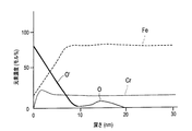
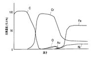
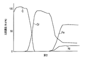
- FIG. 29 is a drawing showing the element concentration profile in the stacking direction of the sample (III-1) measured by AES and before the endurance test.
- FIG. 30 is a drawing showing the element concentration profile in the stacking direction of sample (III-1) after the endurance test, measured by AES.
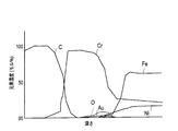
- FIG. 31 is a drawing showing the element concentration profile in the stacking direction of sample (III-2) after the endurance test, measured by AES.
- FIG. 32 is a drawing showing the element concentration profile in the stacking direction of sample (III-3) after the endurance test, measured by AES.
- FIG. 33 is a drawing showing the element concentration profile in the stacking direction of sample (III-4) after the endurance test, measured by AES.
- FIG. 34 is a schematic cross-sectional view showing the configuration of the surface of the gas diffusion layer according to the fourth embodiment.
- FIG. 35 is a schematic view microscopically showing the surface of the porous material layer.
- FIG. 36 is a schematic view showing changes in fibers in each manufacturing process of PAN-based carbon fibers.
- FIG. 37 is a schematic diagram showing an intermediate layer or conductive carbon layer deposition apparatus using a sputtering method.
- FIG. 38 is a diagram showing a general PAN-based carbon fiber manufacturing process and a PAN-based carbon fiber manufacturing process in the fourth embodiment.
- FIG. 39 is a diagram showing a method for measuring the contact resistance between the GDL obtained in Example IV-1 and Comparative Examples IV-1 and IV-2 and the separator.
- FIG. 40 is a graph corresponding to the results regarding contact resistance of Example IV-1 shown in Table 5.
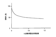
- FIG. 41 is a graph showing the measurement result of the static contact angle of water with respect to the area ratio of conductive carbon and Au, calculated by AES surface mapping and image analysis.
- FIG. 42 is a graph showing the resistance reduction effect when sputtering is performed while Au is dispersed on the surface of the conductive carbon layer.
- FIG. 43 is a schematic cross-sectional view showing the configuration of the conductive member according to the fifth embodiment.
- FIG. 44A is a cross-sectional view schematically showing a contact region between a gas diffusion base composed of carbon fibers or carbon particles and a conductive carbon layer in which conductive particles are dispersed.
- FIG. 44B is a cross-sectional view schematically showing a contact region between a gas diffusion base composed of a porous metal and a conductive carbon layer in which conductive particles are dispersed.
- FIG. 45 is a SEM photograph showing the surface of the conductive carbon layer in which conductive particles (Au) are dispersed in the separator (1).
- FIG. 46 is an SEM photograph showing the surface of the conductive carbon layer in which conductive particles (Au) in the separator (2) are dispersed.
- FIG. 47A is a drawing showing an element concentration profile in the stacking direction of the separator (2), measured by AES.
- FIG. 47B is a drawing showing an element concentration profile in the stacking direction of the separator (4), measured by AES.
- FIG. 48 is a graph showing the results of measurement of contact resistance for the separators produced in the examples and comparative examples.
- FIG. 49 is a graph showing the results of measuring the contact angle for the separators produced in the examples and comparative examples.
- the conductive member (conductive structure) of this embodiment has a metal base material and a conductive carbon layer containing conductive carbon located on at least one surface of the metal base material. And the intensity ratio R (I D / I G ) between the D band peak intensity (I D ) and the G band peak intensity (I G ) measured by the Raman scattering spectroscopic analysis of the conductive carbon layer is 1.3 or more. It is.
- the conductive member of the present embodiment is preferably provided with a metal base and an intermediate layer on the metal base, and the conductive carbon layer is coated on the intermediate layer. And it is desirable for the said intermediate
- the crystalline structure of the conductive carbon layer varies. Therefore, if the crystal structure of such a conductive carbon layer is different, the corrosion resistance and conductivity of the separator itself greatly vary due to this. In other words, it becomes difficult to stably control the fuel cell.
- the metal separator provided by the prior art has sufficient corrosion resistance and conductivity that can withstand practical use even if it has been subjected to a surface treatment such as the arrangement of a conductive carbon layer. It could not be said that the sex was secured.
- the crystal structure of the intermediate layer is controlled even if an intermediate layer such as a metal layer or its carbide layer is provided to ensure adhesion. There wasn't.
- the anticorrosion function of the base material and the denseness of the conductive carbon film are insufficient, water molecules penetrate into the metal base material, and the corrosion resistance of the base material is promoted, resulting in an increase in contact resistance. It was.
- positioned on the base-material surface itself is a layer with high insulation. For this reason, the problem that the electroconductivity of the thickness direction of a separator fell has arisen.
- the columnar structure crystal of the intermediate layer is thickened as a measure for enhancing the anticorrosion function.
- a metal base material such as aluminum, which is easily corroded
- the columnar structure crystal of the intermediate layer is thickened as a measure for enhancing the anticorrosion function.
- the present invention is an epoch-making thing that can reduce gaps and defects in the conductive carbon layer. Further, the protruding particles present in the outermost layer are caused by the development of the column diameter of the columnar structure of the intermediate layer, and the number of gaps in the outermost layer is reduced, and a function of suppressing water intrusion can be provided. . As a result, the anticorrosion effect of the metal substrate can be enhanced, and while being lightweight and inexpensive like aluminum, it can be stably applied as a separator substrate for a long time even in the case of a metal that is easily corroded.
- the columnar structure of the intermediate layer is preferably a columnar crystal.
- the columnar crystal that is the best as the columnar structure of the intermediate layer, but it is not necessarily limited to the columnar crystal and can be widely applied to the columnar structure. .
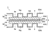
- FIG. 1 is a cross-sectional view schematically showing a basic configuration of a fuel cell using a metal separator, which is an example of a conductive member of the present embodiment, specifically a basic configuration of a cell unit of a polymer electrolyte fuel cell (PEFC). is there.
- FIG. 2 is a partial cross-sectional view showing an outline of a layer formed on the surface of the base material of the metal separator of FIG.
- a solid polymer electrolyte membrane 2 and a pair of catalyst layers 3 sandwiching the solid polymer electrolyte membrane 2 on both sides thereof are provided.
- the laminate of the solid polymer electrolyte membrane 2 and the catalyst layer 3 (3a, 3b) is further sandwiched between a pair of gas diffusion layers 4 (anode gas diffusion layer 4a and cathode gas diffusion layer 4b).
- the solid polymer electrolyte membrane 2, the pair of catalyst layers (3a, 3b), and the pair of gas diffusion layers (4a, 4b) constitute a membrane electrode assembly (MEA) 9 in a stacked state.
- the MEA 9 is further sandwiched by a pair of conductive metal separators 5 (an anode separator 5a and a cathode separator 5b) to constitute the cell unit 1.
- the metal separators 5 a and 5 b are illustrated so as to be located on both sides of the MEA 9.
- the metal separator 5 is generally used also as a metal separator 5 for an adjacent PEFC (see FIGS. 13 and 14).
- the MEAs 9 are sequentially stacked via the metal separator 5 to constitute a stack.
- a gas seal portion is disposed between the metal separators 5a and 5b and the solid polymer electrolyte membrane 2, or between the cell unit 1 and another cell unit 1 adjacent thereto.
- these descriptions are omitted in FIGS. 1 and 2 (see FIGS. 13 and 14).
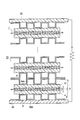
- the metal separator 5 (5a, 5b) is obtained, for example, by forming a concavo-convex shape as shown in FIGS. 1, 2, and 13 by subjecting a thin plate having a thickness of 0.5 mm or less to a press treatment.
- the convex part seen from the MEA 9 side of the metal separator 5 is in contact with the MEA 9. Thereby, the electrical connection with MEA9 is ensured.
- a recess (a space between the metal separator 5 and the MEA 9 generated due to the uneven shape of the metal separator 5) as viewed from the MEA 9 side of the metal separator 5 is used to circulate gas during the operation of the PEFC 1. Functions as a gas flow path.
- the fuel gas 5ag is circulated through the gas flow path 5aa of the anode separator 5a, and the oxidant gas 5bg is circulated through the gas flow path 5bb of the cathode separator 5b.
- the fuel gas 5ag for example, hydrogen or a hydrogen-containing gas can be used
- the oxidant gas 5bg for example, air or an O 2 -containing gas can be used.
- the recess viewed from the side opposite to the MEA 9 side of the metal separator 5 serves as a refrigerant flow path 8 for circulating the refrigerant 8w for cooling the PEFC during operation of the PEFC 1.
- the refrigerant 8w for example, cooling water or water can be used.
- the metal separator 5 is usually provided with a manifold (not shown). This manifold functions as a connection means for connecting the cell units 1 when a stack is formed. With such a configuration, the mechanical strength of the fuel cell stack can be ensured (see FIGS. 13 and 14).
- a gas seal is disposed between the metal separator 5 and the end of the electrolyte membrane 2 and between another cell unit 1 adjacent to the cell unit 1 of the fuel cell. Omitted.
- the metal separator 5 has gas flow paths 5aa and 5bb that flow different fluids such as the fuel gas 5ag, the oxidant gas 5bg, and the refrigerant 8w, and the refrigerant flow.
- a path 8 and a manifold are provided, and further, there is a function of maintaining the mechanical strength of the stack.
- a perfluorosulfonic acid type membrane is usually used as the electrolyte membrane 2
- the inside of the battery is weakly wet due to various acidic ions eluted from the electrolyte membrane and the humidified gas introduced into the battery. Under an acidic corrosive environment. For this reason, as shown in FIG.
- the surface treatment of the metal separator 5 requires not only conductivity but also corrosion resistance.
- the surface treatment layer 7 disposed on the metal substrate 6 of the metal separator 5 is essential to be applied to the reaction surface having severe corrosion conditions.
- the reaction surface 7a is different from the cooling surface 7b. The same processing is required depending on the type and environment of the refrigerant (cooling water) 8w.
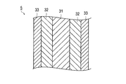
- FIG. 3 is a cross-sectional view showing one form of the surface portion of the metal separator 5.
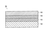
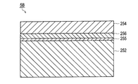
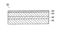
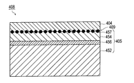
- the conductive member constituting the metal separator 5 includes a metal base 31 and a conductive carbon layer 33. An intermediate layer 32 is interposed between them.
- the metal separator 5 is arranged so that the conductive carbon layer 33 is located on the MEA 9 side.
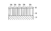
- FIG. 4A is a partial cross-sectional view showing the configuration and arrangement of each layer formed on the surface of the metal substrate of the metal separator, and is a simplified diagram for explaining functions required for each layer for surface treatment.
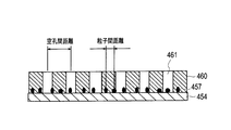
- FIG. 4B is an enlarged view in which a part of FIG. 4A is enlarged to further clarify the configuration of an intermediate layer having a thick columnar crystal structure and a conductive carbon layer in which protruding particles are present on the outermost surface. is there.
- FIG. 4C is an enlarged view that clarifies the configuration of the metal base material of the separator, the intermediate layer having a thin acicular crystal structure, and the conductive carbon layer having no protruding particles on the outermost surface.
- the conductive members constituting the metal separator 5 are the metal base 31 (reference numeral 6 in FIG. 2) and the conductive carbon layer 33 (part of reference numeral 7 in FIG. 2: outer portion). And have. And between these, the intermediate
- the metal separator 5 has a cross-sectional configuration in which an intermediate layer 32 and an outermost conductive carbon layer 33 are disposed on both main surfaces (surfaces) of the metal base 31 of the metal separator 5.
- an intermediate layer 32 and an outermost conductive carbon layer 33 are disposed on both main surfaces (surfaces) of the metal base 31 of the metal separator 5.
- the corrosion of the metal base material 31 of the metal separator 5 depends on the weak acid (acidity) in the battery and the surface potential of the metal separator 5. For this reason, when aluminum is used as the metal substrate 31 of the metal separator 5, it is necessary to prevent corrosion against acidity and potential. However, since the corrosion itself occurs for the first time due to the presence of water, a surface treatment in which the aluminum of the metal base 31 is not in contact with water as much as possible will take a countermeasure against the corrosion, and the effect is very great. For this reason, even if defects such as pinholes occur in the outermost conductive carbon layer 33, the penetration of water into the separator below the intermediate layer 32 is suppressed by controlling the crystal structure of the intermediate layer 32. Therefore, the expected excellent battery performance can be stably maintained for a long time.
- each component of the metal separator 5 of this embodiment is explained in full detail.
- the metal substrate 31 is a main layer of a conductive member that constitutes the metal separator 5, and contributes to ensuring conductivity and mechanical strength.
- the constituent material of the metal substrate 31 examples include iron, titanium, copper, aluminum, and alloys thereof. These materials are preferably used from the viewpoints of mechanical strength, versatility, cost performance, or processability.
- the iron alloy includes stainless steel.
- the metal base material 31 is comprised from stainless steel, aluminum, or aluminum alloy.
- the GDL is composed of a portion where the surface pressure is directly applied to the GDL 4 (4a, 4b) (the metal separator 5 and the contact portion; a rib portion) and a portion that is not directly applied (the portion that is not in contact; the flow path portion).
- the rib shoulder portion refers to the shoulder portion of the contact portion with the metal separator 5.
- Examples of stainless steel include austenite, martensite, ferrite, austenite / ferrite, and precipitation hardening.
- austenite include SUS201, SUS202, SUS301, SUS302, SUS303, SUS304, SUS305, SUS316 (L), and SUS317, which are defined in Japanese Industrial Standards.
- Examples of the austenite-ferrite type include SUS329J1.
- Examples of the martensite system include SUS403 and SUS420.
- Examples of the ferrite type include SUS405, SUS430, and SUS430LX.
- the precipitation hardening system include SUS630.
- austenitic stainless steel such as SUS304 and SUS316.
- the content of iron in the stainless steel is preferably 60 to 84% by mass, more preferably 65 to 72% by mass.
- the chromium content in the stainless steel is preferably 16 to 20% by mass, more preferably 16 to 18% by mass.
- examples of the aluminum alloy include pure aluminum, aluminum / manganese, and aluminum / magnesium.
- the elements other than aluminum in the aluminum alloy are not particularly limited as long as they are generally usable as an aluminum alloy.
- copper, manganese, silicon, magnesium, zinc and nickel are included in the aluminum alloy.
- Specific examples of the aluminum alloy include A1050 and A1050P specified in Japanese Industrial Standards as pure aluminum, A3003P and A3004P as aluminum / manganese, and A5052P and A5083P as aluminum / magnesium. Can be mentioned.
- the separator is also required to have mechanical strength and formability, the alloy tempering is appropriately selected in addition to the above alloy types.
- the metal base material 31 is comprised from the simple substance of titanium or aluminum, the purity of the said titanium or aluminum becomes like this. Preferably it is 95 mass% or more, More preferably, it is 97 mass% or more, More preferably, it is 99 mass % Or more.
- the thickness of the metal substrate 31 is preferably 50 ⁇ m to 500 ⁇ m from the viewpoint of ease of processing and mechanical strength, and improvement of the energy density of the battery by making the separator 5 itself a thin film.
- the thickness of the metal substrate is more preferably 80 ⁇ m to 300 ⁇ m, still more preferably 80 ⁇ m to 200 ⁇ m.
- the thickness of the metal substrate 31 when stainless steel is used is preferably 80 ⁇ m to 150 ⁇ m.
- the thickness of the metal substrate 31 when aluminum is used is preferably 100 ⁇ m to 300 ⁇ m. When it is within the above range, the metal separator 5 has sufficient strength, but is excellent in workability and can achieve a suitable thickness.
- the metal base 31 is preferably made of a material having a high gas barrier property. Since the separator 5 of the fuel cell plays a role of partitioning cells, different gas flows on both sides of the separator 5 (see FIG. 13). Therefore, from the viewpoint of eliminating the mixing of adjacent gases and the fluctuation of the gas flow rate, the metal base 31 is preferably as the gas barrier property is higher.
- the conductive carbon layer 33 is a layer containing conductive carbon. The presence of this layer improves the corrosion resistance as compared with the case of only the metal substrate 31 while ensuring the conductivity of the conductive member constituting the metal separator 5.
- the conductive carbon layer 33 has an intensity ratio R (I D / I G ) between the D band peak intensity (I D ) and the G band peak intensity (I G ) measured by Raman scattering spectroscopy. It is prescribed by. Specifically, the intensity ratio R (I D / I G ) is 1.3 or more.
- R (I D / I G ) is 1.3 or more.
- the intensity ratio R (I D / I G ) between the D band peak intensity (I D ) and the G band peak intensity (I G ) is the graphite cluster size of the carbon material and the disorder of the graphite structure (crystal structure defect), Used as an index such as sp 2 bond ratio. That is, in the present embodiment, the R value can be used as an index of the contact resistance of the conductive carbon layer 33 and can be used as a film quality parameter for controlling the conductivity of the conductive carbon layer 33.
- the R (I D / I G ) value is calculated by measuring the Raman spectrum of the carbon material using a microscopic Raman spectrometer. Specifically, the peak intensity of 1300 ⁇ 1400 cm -1 called the D band (I D), the relative intensity ratio of the peak intensity of 1500 ⁇ 1600 cm -1 called the G band (I G) (peak area ratio ( I D / I G )).
- the R value is 1.3 or more.
- the R value is preferably 1.4 to 2.0, more preferably 1.4 to 1.9, and further preferably 1.5 to 1.8. If the R value is 1.3 or more, the conductive carbon layer 33 in which the conductivity in the stacking direction of the fuel cell is sufficiently secured can be obtained. Moreover, if R value is 2.0 or less, the reduction
- increasing the D-band peak intensity means an increase in crystal structure defects in the graphite structure.
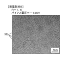
- the conductive member A and the conductive member B use SUS316L as the metal base 31 and have an intermediate layer 32 (thickness: 0.2 ⁇ m) made of Cr and a conductive carbon layer 33 (thickness) on the surface. : 0.2 ⁇ m) was sequentially formed by a sputtering method. Further, the bias voltage applied to the metal base material 31 when the conductive carbon layer 33 in the conductive member A is manufactured is 0 V, and the metal base material 31 is applied when the conductive carbon layer 33 in the conductive member B is manufactured. The applied bias voltage was -140V.
- the conductive carbon layer of the conductive member B has a structure of polycrystalline graphite. That is, it can be seen that there are many graphite clusters 33c. On the other hand, such a structure of polycrystalline graphite cannot be confirmed in the conductive carbon layer of the conductive member A shown in FIG. 5A.
- polycrystalline graphite microscopically has an anisotropic graphite crystal structure (graphite cluster) in which graphene surfaces (hexagonal network surfaces) are laminated, but macroscopically, a large number of such graphite structures. Is an isotropic crystal. Accordingly, it can be said that polycrystalline graphite is a kind of diamond-like carbon (DLC). Normally, single crystal graphite has a disordered structure in which graphene surfaces are laminated even when viewed macroscopically, as represented by HOPG (highly oriented pyrolytic graphite). On the other hand, in polycrystalline graphite, a graphite structure exists as an individual cluster, and has a turbostratic structure.
- HOPG highly oriented pyrolytic graphite
- this degree of disorder (graphite cluster amount, size) is appropriately ensured, and a conductive path from one surface of the conductive carbon layer 33 to the other surface is ensured.
- a decrease in conductivity due to the separate provision of the conductive carbon layer 33 in addition to the metal substrate 31 is prevented.
- an intermediate layer 32 is provided between the metal substrate 31 and the conductive carbon layer 33, and further, the crystal structure is controlled, thereby sufficiently ensuring excellent conductivity. An increase in contact resistance can be suppressed.
- polycrystalline graphite since the graphene surface is formed by the bonding of sp 2 carbon atoms constituting the graphite cluster, conductivity is ensured in the plane direction of the graphene surface.
- Polycrystalline graphite is substantially composed of only carbon atoms, has a small specific surface area, and a small amount of bonded functional groups. For this reason, polycrystalline graphite has excellent resistance to corrosion by acidic water or the like.
- primary particles are often formed by aggregates of graphite clusters, thereby exhibiting electrical conductivity.
- the individual particles are separated, there are many functional groups formed on the surface, and corrosion due to acidic water or the like is likely to occur. Further, even when the conductive carbon layer 33 is formed with carbon black, there is a problem that the denseness as a protective film is lacking.
- the size of the graphite cluster constituting the polycrystalline graphite is not particularly limited.
- the average diameter of the graphite cluster is preferably about 1 nm to 50 nm, more preferably 2 nm to 10 nm.
- the “diameter” of the graphite cluster means the maximum distance among the distances between any two points on the contour line of the cluster.
- the average diameter value of the graphite clusters is calculated as an average value of the diameters of the clusters observed in several to several tens of fields using an observation means such as SEM or TEM.
- a part of the conductive carbon layer 33 is formed on the surface of the intermediate layer 32, and has protruding particles 33a having a diameter of 200 nm to 500 nm. desirable. More preferably, it is particularly desirable that protruding particles 33a having a diameter of 200 nm to 500 nm and fine particles 33b of 50 nm to 100 nm are mixed on the outermost surface of the conductive member (see Example I-8). However, in this embodiment, as shown in FIG. 4C, the protruding particles 33a having a diameter of 200 nm to 500 nm may not be provided on the outermost surface of the conductive member.
- the conductive carbon layer 33 is composed of only fine particles 33b of 50 nm to 100 nm. Also good. Even in such a configuration, if the strength ratio R of the conductive carbon layer 33 is 1.3 or more, the intended object of the present invention can be achieved (see Example I-9).
- an intermediate layer 32 is provided between the conductive carbon layer 33 and the metal substrate 31, the crystal structure of the intermediate layer 32 is controlled, and the column diameter of the columnar crystal is set to the conductive carbon layer 33.
- the protruding particles 33a having a diameter of 200 nm to 500 nm, preferably 300 nm to 500 nm, more preferably 400 nm to 500 nm are present on the outermost surface, the number of gaps on the outermost surface of the conductive member is reduced and water enters. Can be suppressed.
- the fine particles 33b are present in the peripheral portion other than the protruding particles 33a (a flat portion having a small unevenness change amount), it is particularly effective in reducing gaps and defects in the conductive carbon layer 33. .
- the anticorrosion effect of the metal substrate 31 can be enhanced, and even a metal that is easily corroded such as aluminum can be applied as the metal substrate 31.
- the diameter of the protruding particle 33a on the outermost surface of the conductive member is measured by using observation means such as a scanning electron microscope (SEM) or a transmission electron microscope (TEM). It is calculated as an average value of the diameters.
- the size (diameter) of the fine particles 33b on the outermost surface of the conductive member also refers to the range of the particle size distribution.
- the size of the fine particles 33b on the outermost surface of the conductive member can also be measured in the same manner as the protruding particles 33a.
- the particle diameter of the protruding particles 33a can be determined by measuring the maximum length of thin (white) particles having a low contrast from the observation result of the sample surface by SEM.
- the protruding particles 33a be present in the range of at least 30 or more, preferably 30 to 100, more preferably 50 to 80 per 100 ⁇ m 2 .
- the gap in the intermediate layer 32 is reduced, formation of an oxide film inside the surface treatment can be suppressed, and an increase in contact resistance can be suppressed.
- the number of the projecting particles 33a is less than 30 per 100 ⁇ m 2 , since the development of the columnar crystal diameter of the intermediate layer 32 is reduced, the number of gaps between the columnar crystals on the outermost surface of the conductive member is reduced. This may increase the contact resistance.
- the present invention even if the number of the protruding particles 33a per 100 ⁇ m 2 is less than 30, even if it is within the range not impairing the effect of the present embodiment, it is included in the present invention. .
- the conductivity from one surface of the conductive carbon layer 33 to the other surface is controlled. Since the path is secured, a conductive member having sufficiently improved corrosion resistance while sufficiently securing excellent conductivity is provided (FIGS. 4C, 15A, 16A, 17A, 18A, Example I- 9).
- the distance between the vertices of the outermost protruding particles 33a is preferably within 1 ⁇ m (see FIG. 4B).
- the height H of the protruding particles 33a is 100 nm to 500 nm, preferably 200 nm to 500 nm, more preferably 300 nm to 400 nm with respect to the peripheral portion (see FIG. 4B). .
- the height H of the protruding particles 33a is within the above range, the columnar crystal of the intermediate layer 32 grows and the column diameter W of the intermediate layer is increased, so that the gap in the intermediate layer is further reduced. Further, the anticorrosion function of the metal substrate 31 can be further improved.
- the conductive member has a protruding shape in which the protruding particles 33a are present on the outermost surface, the specific surface area is improved.
- the protruding particles 33a are particles that constitute a part of the conductive carbon layer, and further protrude along the protrusions of the intermediate layer.
- the fine particles 33b are particles that constitute a part of the conductive carbon layer but do not protrude as compared with the protruding particles.
- grain can be picked up from the contrast confirmed from the surface observation by SEM, and it can obtain
- the height H (H 1 , H 2 , H 3 ) of the protruding particle 33a is the height from the surface of the microparticle 33b existing around the protruding particle 33a to the tip of the protruding particle 33a.
- the height of the protruding particles 33a can be obtained by cross-sectional observation with a TEM.
- the method for measuring the number of protruding particles 33a having a diameter of 200 to 500 nm per 100 ⁇ m 2 is performed as follows. First, the particle-like thing confirmed as white as contrast by surface observation by SEM is caught as a protruding particle. Next, the number of particles having the above particle diameter present in 100 ⁇ m 2 is measured. (D) Regarding the method for measuring the microparticles 33b having a diameter of 50 to 100 nm, the particles having the above particle diameter can be measured by surface observation with an SEM.
- the conductive carbon layer 33 may be substantially composed only of polycrystalline graphite or may be composed only of polycrystalline graphite, but the conductive carbon layer 33 is other than polycrystalline graphite.
- Other materials may also be included.
- the carbon material other than the polycrystalline graphite include graphite block (highly crystalline graphite), carbon black, fullerene, carbon nanotube, carbon nanofiber, carbon nanohorn, and carbon fibril.
- Specific examples of carbon black include ketjen black, acetylene black, channel black, lamp black, oil furnace black, or thermal black. Carbon black may be subjected to a graphitization treatment. These carbon materials may be used in combination with a resin such as a polyester resin, an aramid resin, or a polypropylene resin.
- gold As a material other than the carbon material included in the conductive carbon layer 33, gold (Au), silver (Ag), platinum (Pt), ruthenium (Ru), palladium (Pd), rhodium (Rh), indium ( A noble metal such as In); a water repellent material such as polytetrafluoroethylene (PTFE); and a conductive oxide.
- gold Au
- silver Ag
- platinum Pt
- Ru palladium
- Rhodium Rh
- indium A noble metal such as In
- a water repellent material such as polytetrafluoroethylene (PTFE); and a conductive oxide.
- PTFE polytetrafluoroethylene
- conductive oxide As for materials other than polycrystalline graphite, only 1 type may be used and 2 or more types may be used together.
- the average particle size when the carbon material other than the polycrystalline graphite is in the form of particles is preferably 2 nm to 100 nm, more preferably 5 nm to 20 nm, from the viewpoint of suppressing the thickness of the conductive carbon layer.
- the “particle diameter” means the maximum distance among the distances between any two points on the particle outline.
- the value of “average particle size” is a value calculated as an average value of the particle size of particles observed in several to several tens of fields using an observation means such as SEM or TEM unless otherwise specified. Shall be adopted.
- the diameter is preferably 0.4 nm to 100 nm, more preferably 1 nm to 20 nm.
- the length in the case of the fibrous form is 5 nm to 200 nm, more preferably 10 nm to 100 nm.
- the aspect ratio in the case of the fibrous form is 1 to 500, more preferably 2 to 100.
- the average thickness of the conductive carbon layer 33 excluding the protruding particles 33a is preferably 1 nm to 1000 nm, more preferably 2 nm to 500 nm, and further preferably 5 nm to 200 nm.
- the thickness of the conductive carbon layer 33 is a value within such a range, sufficient conductivity can be ensured between the gas diffusion base and the metal separator 5.
- the metal base 31 can have a high corrosion resistance function.
- the conductive carbon layer 33 may be present only on one surface of the conductive member (metal separator 5) as shown in FIG. 3, but preferably shown in FIG. 2, FIG. 4A, and the like. Thus, it is desirable that the conductive carbon layers 33 exist on both surfaces of the conductive member. This is because the anticorrosion effect of the metal substrate 31 can be further maintained while securing the adhesion between the metal substrate 31 and the conductive carbon layer 33 via the intermediate layer 32 on both surfaces of the conductive member. .
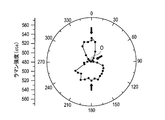
- the average peak measured by the rotational anisotropy measurement of the Raman scattering spectroscopic analysis shows a two-fold symmetry pattern.
- the measurement principle of rotational anisotropy measurement will be briefly described.
- Rotational anisotropy measurement of Raman scattering spectroscopic analysis is performed by performing Raman scattering spectroscopic measurement while rotating the measurement sample 360 degrees in the horizontal direction. Specifically, the surface of the measurement sample is irradiated with laser light, and a normal Raman spectrum is measured. Next, the measurement sample is rotated by 10 °, and the Raman spectrum is measured in the same manner. This operation is performed until the measurement sample rotates 360 °. And the average peak is obtained by calculating the average value of the peak intensities obtained at the respective angles, and displaying the weakest of the measured peak intensities as the center O and displaying the polar coordinates at 360 ° per revolution. .
- FIG. 6A when the graphite layer is present on the sample surface so that the graphene surface is parallel to the surface direction of the sample, a three-fold symmetry pattern as shown in FIG. 6A can be seen.
- FIG. 6B when the graphite layer is present on the sample surface so that the graphene surface is perpendicular to the surface direction of the sample, a two-fold symmetry pattern as shown in FIG. 6B can be seen.
- FIG. 6C When an amorphous carbon layer having no clear crystal structure is present on the sample surface, a pattern not showing symmetry as shown in FIG. 6C can be seen.
- the conductivity in the conductive carbon layer 33 is ensured by the shortest path, which is preferable.
- FIGS. 7A and 7B show the results of the rotational anisotropy measurement described above.
- FIG. 7A shows a Raman spectrum when the conductive member B is used as a measurement sample and the rotation angles of the sample are 0 °, 60 °, and 180 °, respectively.
- FIG. 7B shows an average peak of rotational anisotropy measurement for the conductive member B obtained by the above-described method. As shown in FIG. 7B, in the measurement of rotational anisotropy of the conductive member B, peaks were observed at 0 ° and 180 ° positions. This corresponds to the two-fold symmetry pattern shown in FIG. 6B. In this specification, “showing a two-fold symmetry pattern” means that, as shown in FIG.
- the Vickers hardness of the conductive carbon layer 33 is defined.
- “Vickers hardness (Hv)” is a value that defines the hardness of a substance, and is a value inherent to the substance.
- the Vickers hardness means a value measured by a nanoindentation method.
- the nanoindentation method is a method in which the diamond indenter is continuously loaded and unloaded with a very small load on the sample surface, and the hardness is measured from the obtained load-displacement curve. Larger means that the substance is harder.
- the Vickers hardness of the conductive carbon layer 33 is preferably 1500 Hv or less, more preferably 1200 Hv or less, further preferably 1000 Hv or less, and particularly preferably 800 Hv or less. .
- the Vickers hardness is a value within such a range, excessive mixing of sp 3 carbon having no conductivity is suppressed, and a decrease in the conductivity of the conductive carbon layer 33 can be prevented.
- the lower limit value of the Vickers hardness is not particularly limited, but if the Vickers hardness is 50 Hv or more, the hardness of the conductive carbon layer 33 is sufficiently ensured.
- the conductive member (separator 5) that can withstand impacts such as external contact and friction, and has excellent adhesion to the metal substrate 31 as a base.
- the intermediate layer 32 is provided as in the present embodiment, it is possible to provide a conductive member that is more excellent in adhesion than the conductive carbon layer 33 and the intermediate layer 32 and further the metal base 31. it can.
- the Vickers hardness of the conductive carbon layer 33 is more preferably 80 Hv or more, further preferably 100 Hv or more, and particularly preferably 200 Hv or more.
- SUS316L is prepared as the metal base 31 of the conductive member.
- an intermediate layer 32 (thickness 0.2 ⁇ m) made of Cr and a conductive carbon layer 33 (thickness 0.2 ⁇ m) were sequentially formed by sputtering.
- the average value of the columnar crystal column thickness in the cross section of the intermediate layer 32 is 200 nm to 500 nm, and the columnar crystal having this thickness is electrically conductive in the entire intermediate layer 32. 60% of the total thickness of the intermediate layer is present on the carbonaceous carbon layer 33 side.
- the conductive carbon layer 33 has a mixture of protruding particles 33a having a diameter (particle size distribution) of 200 nm to 500 nm and fine particles 33b of 50 nm to 100 nm on the outermost surface, and the protruding particles 33a are mixed. There are 60 on average per 100 ⁇ m 2 .
- the crystal structure of the intermediate layer 32 is controlled to create a columnar crystal diameter having a desired column diameter and number, and then the Vickers hardness of the conductive carbon layer 33. Changed.
- FIG. 8 shows the relationship between the Vickers hardness of the conductive carbon layer 33 and the value of the sp 3 ratio in the conductive member thus obtained.
- FIG. 8 shows the relationship between the Vickers hardness of the conductive carbon layer 33 and the value of the sp 3 ratio in the conductive member thus obtained.
- the amount of hydrogen atoms contained in the conductive carbon layer 33 it is preferable to consider the amount of hydrogen atoms contained in the conductive carbon layer 33. That is, when the conductive carbon layer 33 includes a hydrogen atom, the hydrogen atom is bonded to the carbon atom. Then, the hybrid orbital of the carbon atom to which the hydrogen atom is bonded is changed from sp 2 to sp 3 and the conductivity is lost, and the conductivity of the conductive carbon layer 33 is lowered. Further, when the C—H bond in the polycrystalline graphite is increased, the continuity of the bond is lost, the hardness of the conductive carbon layer 33 is lowered, and finally the mechanical strength and corrosion resistance of the conductive member are lowered. .
- the content of hydrogen atoms in the conductive carbon layer 33 is preferably 30 atomic percent or less, more preferably 20 atomic percent or less, with respect to all atoms constituting the conductive carbon layer 33. More preferably, it is 10 atomic% or less.
- a value obtained by elastic recoil scattering analysis (ERDA) is adopted as the value of the hydrogen atom content in the conductive carbon layer 33. In this method, a measurement sample is tilted, and a helium ion beam is incident shallowly, thereby detecting an element ejected forward. Since the nucleus of a hydrogen atom is lighter than the incident helium ion, if a hydrogen atom is present, the nucleus is ejected forward.
- the energy spectrum of the ejected atom reflects the mass of the nucleus. Therefore, the content of hydrogen atoms in the measurement sample is measured by measuring the number of nuclei of the ejected hydrogen atoms with a solid detector.
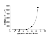
- FIG. 9 is a graph showing the results of measuring the contact resistance of several conductive members having the conductive carbon layer 33 having the above-described R value of 1.3 or more but having different hydrogen atom contents. It is. As shown in FIG. 9, when the content of hydrogen atoms in the conductive carbon layer 33 is 30 atomic% or less, the value of the contact resistance of the conductive member is significantly reduced.
- SUS316L was used as the metal base 31 of the conductive member.
- An intermediate layer 32 (thickness 0.2 ⁇ m) made of Cr and a conductive carbon layer 33 (thickness 0.2 ⁇ m) were sequentially formed on the surface by sputtering. At this time, the hydrogen atom content in the conductive carbon layer was changed by controlling the film formation method and the amount of hydrocarbon gas.
- the entire metal base 31 is covered with the conductive carbon layer 33 through the intermediate layer 32.
- the ratio (coverage) of the area where the metal base 31 is covered with the conductive carbon layer 33 is 100%.
- a coverage may be less than 100%.
- the coverage of the metal substrate 31 by the conductive carbon layer 33 is preferably 50% or more, more preferably 80% or more, still more preferably 90% or more, and most preferably 100%.
- the coverage is determined by viewing the conductive member (metal separator 5) from the stacking direction.
- the ratio of the area of the metal substrate 31 overlapping with the conductive carbon layer 33 is meant.
- the conductive member constituting the metal separator 5 has an intermediate layer 32.
- the intermediate layer 32 has a function of improving the adhesion between the metal substrate 31 and the conductive carbon layer 33 and a function of preventing elution of ions from the metal substrate 31.
- the R value exceeds the upper limit of the preferable range described above, the effect of providing the intermediate layer 32 is remarkably exhibited.
- the intermediate layer 32 is provided even when the R value is included in the preferred range described above. From another point of view, the above-described operation and effect due to the installation of the intermediate layer 32 are more prominently exhibited when the metal substrate 31 is made of aluminum or an alloy thereof.
- middle layer 32 is demonstrated.
- the columnar crystal structure refers to a structure in which the crystals constituting the intermediate layer grow in a columnar shape in the film thickness direction.
- (B) The method for measuring the average value of the column thickness W of the columnar crystals in the cross section of the intermediate layer is determined as follows. First, from a cross-sectional observation result by TEM, for a columnar crystal growing in a direction perpendicular to the metal substrate 31, one column is specified from the interface of the column confirmed by contrast, and is parallel to the metal substrate. It can be obtained by calculating the distance from one interface in the direction to the other interface.
- the thickness of the columnar crystal column in the cross section of the intermediate layer is 200 to 500 nm, and the columnar crystal having the thickness of the intermediate layer has the entire intermediate layer thickness on the conductive carbon layer side of the entire intermediate layer.
- the percentage is calculated as follows. As shown in FIG. 4B, the ratio (T 2 / T 1 ) of the thickness T 2 of the columnar crystal having the above thickness with respect to the average thickness T 1 of the intermediate layer is obtained from the cross-sectional observation result by TEM.
- the thickness T 1 of the intermediate layer the thickness excluding the height H 4 of the projections 32a in the intermediate layer.
- the conductive carbon layer side in the entire intermediate layer refers to a 50% region on the conductive carbon layer side in the thickness direction of the intermediate layer.
- the measuring method of the film thickness (average value) of the intermediate layer can be read from the cross-sectional observation result by SEM or TEM.
- the intermediate layer 32 has a columnar crystal structure. And although mentioned later for details, it is desirable to form the intermediate
- the intermediate layer 32 is provided between the conductive carbon layer 33 and the metal substrate 31, the columnar crystal structure of the intermediate layer 32 is controlled, and the column diameter of the columnar crystal is set to be conductive.
- columnar protrusions (convex portions) are formed on the surface of the intermediate layer 32.
- the conductive carbon layer 33 thereon the conductive carbon layer 33 is formed along the undulations on the surface of the intermediate layer 32.
- a conductive member having a structure in which the intermediate layer 32 has a columnar crystal structure and the protruding particles 33a exist on the outermost surface of the conductive member is provided.
- the gap between the columnar crystals of the intermediate layer 32 and the conductive carbon present thereon are formed.
- the gaps and defects in the layer 33 are greatly reduced. That is, the protruding particles 33a are due to the development of the columnar diameter of the intermediate layer 32, and the number of outermost layer gaps can be reduced to provide a function of suppressing water intrusion.
- a material that imparts the above-mentioned adhesion is preferable.
- Group 4 metals Ti, Zr, Hf
- Group 5 metals V, Nb, Ta
- Group 6 metals Cr, Mo, W
- their carbides nitriding And carbonitrides.
- metals with low ion elution such as chromium (Cr), tungsten (W), titanium (Ti), molybdenum (Mo), niobium (Nb) or hafnium (Hf), or their nitrides, carbides or charcoal are preferable.
- Nitride is used.
- Cr or Ti or a carbide or nitride thereof is used.
- the role of the intermediate layer 32 is to ensure adhesion with the upper conductive carbon layer 33 and to prevent corrosion of the underlying metal substrate 31.
- the metal substrate 31 made of aluminum or an alloy thereof corrosion proceeds due to moisture reaching the vicinity of the interface, and an aluminum oxide film is formed. As a result, the conductivity in the film thickness direction of the entire metal base 31 is deteriorated.
- Chromium and titanium are particularly useful in that, due to the formation of a passive film, even if exposed portions are present, their own elution is hardly observed.
- the metal especially Cr or Ti
- the average value of the columnar crystal column thicknesses W 1 , W 2 , W 3 in the cross section of the intermediate layer 32 is 200 nm to 500 nm, preferably 300 nm to 500 nm, more preferably 400 nm to 500 nm. It is desirable that By having the columnar crystals having a thickness within such a range that the average column thickness of the columnar crystals in the cross section of the intermediate layer 32 is present, the amount of gaps between the columnar crystals is reduced, and the penetration of moisture reaching the metal substrate 31 Can be suppressed.
- the intermediate layer 32 When providing the intermediate layer 32, it is preferable to control the crystal structure of the intermediate layer 32 so that the column diameter of the columnar crystals of the intermediate layer 32 is increased to the interface with the conductive carbon layer 33. Thereby, the clearance gap and defect in the conductive carbon layer 33 formed on it can be remarkably reduced.
- the particle diameter of the protruding particles 33a in the outermost layer of the conductive member (metal separator 5) is closely related to the column diameter of the columnar crystals. And when the column diameter of the columnar crystal is increased and the particle diameter of the protruding particles 33a is 200 nm to 500 nm, the number of gaps in the outermost layer of the conductive member is reduced, and the function of suppressing water intrusion is achieved. Can be granted.
- the thickness of the columnar crystal column in the cross section is preferably 200 nm to 500 nm. Further, regarding the columnar crystal having the thickness, 5 to 95% of the total thickness of the intermediate layer 32 is constituted by the columnar crystal having the thickness, and the columnar crystal having the thickness is further on the conductive carbon layer 33 side. It is desirable to exist. In the present embodiment, it is desirable that the thickness of the columnar crystal on the outermost surface of the intermediate layer 32 is maintained up to the interface between the metal base 31 and the intermediate layer 32 as much as possible. However, when the intermediate layer 32 is first formed on the metal substrate 31, it is necessary to increase the energy applied to the surface in order to thicken the columnar crystals from the beginning.
- the thickness of the columnar crystal on the metal substrate 31 side is preferably thinner than that on the conductive carbon layer 33 side.
- the anticorrosion effect of the metal substrate 31 can be maintained more stably while ensuring the adhesion between the metal substrate 31 and the conductive carbon layer 33.
- the columnar crystal column thickness in the cross section is 200 to 500 nm, preferably 200 to 400 nm, and more preferably 200 to 300 nm.
- the columnar crystals having the above thickness are present in an amount of 5 to 95%, preferably 20 to 90%, more preferably 50 to 90% of the entire thickness of the intermediate layer 32, and the columnar crystals having the above thickness are further conductive. It is preferably formed on the side of the carbonaceous layer 33.
- the thickness of the intermediate layer 32 is not particularly limited. However, from the viewpoint of making the size of the fuel cell stack as small as possible by making the metal separator 5 thinner, the thickness of the intermediate layer 32 is preferably 0.01 ⁇ m to 10 ⁇ m, more preferably 0.02 ⁇ m. Is 5 ⁇ m, more preferably 0.05 ⁇ m to 5 ⁇ m, and particularly preferably 0.1 ⁇ m to 1 ⁇ m. If the thickness of the intermediate layer 32 is 0.01 ⁇ m or more, a uniform layer is formed, and the corrosion resistance of the metal substrate 31 can be effectively improved.
- the thickness of the intermediate layer 32 is 10 ⁇ m or less, an increase in the film stress of the intermediate layer 32 is suppressed, and a decrease in film followability to the metal substrate 31 and occurrence of peeling / cracking associated therewith are prevented. .
- the thickness of the intermediate layer 32 is 0.02 ⁇ m to 5 ⁇ m.
- the intermediate layer 32 has a film thickness within the above range, it is more desirable to have the following configuration. That is, columnar crystals having a thickness of 200 nm to 500 nm on the surface of the intermediate layer 32 on the side of the conductive carbon layer 33 are the entire thickness of the intermediate layer 32 with respect to the direction from the conductive carbon layer 33 to the metal substrate 31. It is desirable to maintain at 5% or more.
- the columnar crystals having the above thickness are preferably in the range of 20 to 90%, more preferably 50 to 90% of the entire thickness of the intermediate layer 32 with respect to the direction from the conductive carbon layer 33 to the metal substrate 31. It is desirable that it be maintained.
- the film thickness of the intermediate layer 32 is less than 0.02 ⁇ m, the columnar crystal structure of the intermediate layer 32 is undeveloped, and it is difficult to maintain the denseness.
- the film thickness of the intermediate layer 32 exceeds 5 ⁇ m, the film stress increases and the adhesiveness with the metal substrate 31 is deteriorated, so that cracks and peeling may occur.
- the thickness of the intermediate layer 32 may be increased to about 10 ⁇ m as long as the intended effect of the present invention is not impaired.
- the intermediate layer 32 has such a three-dimensional structure, the anticorrosion effect of the metal substrate 31 can be maintained more stably while strengthening the adhesion between the metal substrate 31 and the conductive carbon layer 33.
- the surface of the intermediate layer 32 on the side of the conductive carbon layer 33 is preferably formed with irregularities at the nano level. According to such a form, the adhesion of the conductive carbon layer 33 to the intermediate layer 32 is further improved.
- the thermal expansion coefficient of the intermediate layer 32 is a value close to the thermal expansion coefficient of the metal constituting the metal substrate 31, the adhesion between the intermediate layer 32 and the metal substrate 31 is improved. However, in such a form, the adhesion between the intermediate layer 32 and the conductive carbon layer 33 may be reduced. Similarly, when the thermal expansion coefficient of the intermediate layer 32 is close to the thermal expansion coefficient of the conductive carbon layer 33, the adhesion between the intermediate layer 32 and the metal substrate 31 may be lowered.
- the thermal expansion coefficient ( ⁇ mid ) of the intermediate layer 32, the thermal expansion coefficient ( ⁇ sub ) of the metal base 31, and the thermal expansion coefficient ( ⁇ c ) of the conductive carbon layer 33 are expressed by the following relationship: Is preferably satisfied.
- the intermediate layer 32 only needs to be present on at least one surface of the metal substrate 31, and is desirably present on both surfaces of the metal substrate 31.
- the conductive carbon layer 33 may be present on both surfaces of the metal base 31.
- the intermediate layer 32 is preferably interposed between the metal base 31 and both conductive carbon layers 33, respectively.
- the intermediate layer 32 is disposed on the MEA 9 side. It is preferable that it exists in.
- an aluminum plate having a desired thickness, an alloy plate thereof, a titanium plate, a stainless steel plate, or the like is prepared.
- the surface of the constituent material of the prepared metal base 31 is degreased and cleaned using an appropriate solvent.
- the solvent ethanol, ether, acetone, isopropyl alcohol, trichloroethylene, a caustic agent, or the like can be used.
- the degreasing and cleaning treatment include ultrasonic cleaning.
- the ultrasonic cleaning conditions are a processing time of about 1 to 10 minutes, a frequency of about 30 to 50 kHz, and a power of about 30 to 50 W.
- the oxide film formed on the surface of the constituent material of the metal base 31 is removed.
- the method for removing the oxide film include a cleaning treatment with an acid, a dissolution treatment by applying a potential, or an ion bombardment treatment.
- a method in which alkali immersion cleaning, removal of an oxide film with alkali (alkali etching), surface activation with a hydrofluoric acid mixed acid solution, and subsequent zincate treatment in a zinc substitution bath is preferably used.
- the conditions for the zincate treatment are not particularly limited.
- the bath temperature is 10 to 40 ° C. and the immersion time is 20 to 90 seconds. Note that the oxide film removing step may be omitted.
- the treatment is preferably performed on at least the surface of the metal plate on which the intermediate layer is formed, but more preferably on both surfaces of the metal plate.
- a conductive carbon layer 33 is formed on the surface of the constituent material of the metal base 31 subjected to the above-described treatment.
- the conductive carbon layer 33 is formed by laminating a layer containing conductive carbon on the metal substrate 31 at the atomic level using the constituent material (for example, graphite) of the conductive carbon layer 33 described above as a target. be able to.
- the adhesion between the interface between the conductive carbon layer 33 and the metal substrate 31 directly adhered thereto and the vicinity thereof is maintained for a long period of time due to intermolecular force and the entry of a few carbon atoms.
- the metal base 31 is formed before the conductive carbon layer 33 is formed.
- a step of forming the intermediate layer 32 on at least one surface of the substrate is performed.
- the same method as described later for the formation of the conductive carbon layer 33 is employed. However, it is necessary to change the target to the constituent material of the intermediate layer 32.
- the negative bias voltage it is preferable to change the negative bias voltage from a low value to a high value when the intermediate layer 32 is formed.
- a low bias voltage if it exceeds 0 V is selected so as not to deteriorate the roughness of the interface with the metal substrate 31.
- the film formation is started at 0V to 50V.
- the bias voltage is shifted to a high value (usually 50 to 500 V, preferably 100 to 250 V) to grow the columnar crystal thickly.
- the optimum columnar crystal structure can be controlled through preliminary experiments and the like.
- film formation may be started at a low bias voltage so as not to deteriorate the roughness of the interface with the metal substrate 31, and for example, initially, it may be over 0V to 50V. After that, there is no problem even if there is a region where the value changes from a high value to a low value, for example, 120V ⁇ 90V ⁇ 200V. This is because when the bias voltage is a low value, the column diameter of the columnar crystal is small, when the bias voltage is high, the column diameter is large, and after that, the column diameter at a high value can be maintained even if it is changed to a low value or the like. Because.
- the film formation is started at a low bias voltage so as not to deteriorate the roughness of the interface with the metal substrate 31, and then the bias voltage is shifted to a high value. Regardless of the change in voltage thereafter, the columnar crystal can be grown thick.
- the conductive carbon layer 33 is formed along the thick columnar crystal of the intermediate layer 32.
- the intermediate layer 32 has a columnar crystal structure and the protruding particles 33a are present on the outermost surface by a simple method of changing the set value of the apparatus. it can.
- the intermediate layer 32 is formed on the metal base 31 for the first time, in order to thicken the column from the beginning, energy applied to the surface of the metal base 31 is increased, which may cause poor adhesion.
- the columnar crystal on the metal base 31 side is preferably thinner than the conductive carbon layer 33 side. Therefore, at the initial stage of forming the intermediate layer 32, it is preferable to start the film formation with a low bias voltage so as not to deteriorate the roughness of the interface with the metal substrate 31.
- the columnar crystals of the intermediate layer 32 can be thickened to the interface with the conductive carbon layer 33, and gaps and defects in the conductive carbon layer 33 formed thereon can be reduced.
- a sputtering method is preferable as a method for changing the negative bias voltage from a low value to a high value.
- the conductive carbon layer 33 is also preferably formed by a sputtering method.
- the intermediate layer 32 formed before that is preferably formed by a similar dry process, particularly by a sputtering method. In this case, since the intermediate layer 32 can be formed by the same method and the same apparatus as the conductive carbon layer 33, the manufacturing process cost can be reduced.
- the step of forming the intermediate layer 32 it is desirable that a film is formed on the surface of the metal base 31 by sputtering after the surface of the metal base 31 is subjected to pretreatment such as polishing.
- pretreatment such as polishing.
- the pretreatment in addition to the polishing treatment, a treatment that is generally performed can be widely adopted. For example, electrolytic polishing, lapping treatment, microshot treatment, etc. can be applied.
- the intermediate layer 32 and the conductive carbon layer 33 are sequentially formed on the surface of the constituent material of the metal base 31 subjected to the above treatment.
- the chromium intermediate layer 32 is formed on both surfaces of the metal base 31 (for example, aluminum or an alloy thereof) by the above-described bias change using the constituent material of the intermediate layer 32 (for example, chromium) as a target.
- Laminate the layer 33 containing conductive carbon is laminated on the surface of the intermediate layer 32 on the surface of the intermediate layer 32 using the constituent material (for example, graphite) of the conductive carbon layer 33 as a target in order.
- the intermediate layer 32 and the conductive carbon layer 33 can be formed sequentially.
- the adhesion between the directly attached conductive carbon layer 33, intermediate layer 32, and metal base 31 and its vicinity is maintained for a long period of time due to intermolecular forces and the ingress of slight carbon atoms.
- a physical vapor deposition (PVD) method such as a sputtering method or an ion plating method, or a filtered cathodic vacuum arc (FCVA) is used.
- PVD physical vapor deposition
- FCVA filtered cathodic vacuum arc
- ion beam deposition methods examples include a magnetron sputtering method, an unbalanced magnetron sputtering (UBMS) method, a dual magnetron sputtering method, and an ECR sputtering method.
- UBMS unbalanced magnetron sputtering
- ECR sputtering method examples of the ion plating method include an arc ion plating method.
- sputtering method and an ion plating method it is preferable to use sputtering method and an ion plating method, and it is especially preferable to use sputtering method.
- a carbon layer having a low hydrogen content can be formed.
- the ratio of bonds between carbon atoms (sp 2 hybrid carbon) can be increased, and excellent conductivity is achieved.
- the film can be formed at a relatively low temperature, and there is an advantage that damage to the metal substrate 31 can be minimized.
- the intermediate layer 32 having the columnar crystal structure can be obtained by controlling the bias voltage or the like.
- the intermediate layer 32 and the conductive carbon layer 33 are formed by the sputtering method, it is preferable to apply a negative bias voltage to the metal substrate 31 during the sputtering.
- the intermediate carbon layer 32 having the columnar crystal structure and the conductive carbon layer 33 in which graphite clusters are densely assembled are formed by the ion irradiation effect.
- Such an intermediate layer 32 can enhance the anticorrosive effect of the metal substrate 31 and can be applied as the metal substrate 31 even in the case of a metal that is easily corroded such as aluminum.
- the conductive carbon layer 33 exhibits excellent conductivity, the metal separator 5 having a low contact resistance with other members (for example, the MEA 9) is provided.
- the absolute value of the negative bias voltage to be applied is not particularly limited, and a voltage capable of forming the conductive carbon layer 33 is employed.
- the magnitude of the applied voltage is preferably 50 to 500V, more preferably 100 to 300V.
- a method of changing the negative bias voltage during film formation from a low value to a high value is suitable. Specifically, as in the examples described later, in the initial stage of film formation of the intermediate layer 32, film formation is started with a low bias voltage (above 0 V to 50 V), and then the bias voltage is increased to a high value (usually 50 to 500 V). (Preferably, the columnar crystal structure is grown thickly by shifting to 100 to 250 V).
- film formation may be started with a low bias voltage, and thereafter, there is a region where the value changes from a high value to a low value, such as 120V ⁇ 90V ⁇ 200V. There is no problem even if it exists.
- the conductive carbon layer 33 is formed by the UBMS method, it is preferable to form the intermediate layer 32 in advance by the same apparatus and manufacturing method, and form the conductive carbon layer 33 thereon. Thereby, the intermediate
- the intermediate layer 32 may be formed by another method or apparatus, and the conductive carbon layer 33 may be formed by a different apparatus or manufacturing method. Even in this case, the intermediate layer 32 and the conductive carbon layer 33 having excellent adhesion to the metal substrate 31 are formed.
- the conductive carbon layer 33 is formed on the metal base material 31 by another method or apparatus, the conductivity excellent in adhesion to the metal base material 31 even when the intermediate layer 32 is not present.
- the carbon layer 33 is formed.
- the intermediate layer 32 and the conductive carbon layer 33 are formed on one surface of the metal substrate 31.
- the intermediate layer 32 and the conductive carbon layer 33 are formed on the other surface of the metal substrate 31 by the same method. Just do it.
- a conductive member in which the intermediate layer 32 and the conductive carbon layer 33 are formed at the same time on both surfaces of the metal base 31 is manufactured.
- a commercially available film forming apparatus double-sided simultaneous sputtering film forming apparatus
- the intermediate layer 32 and the conductive carbon layer 33 are formed on one surface of the metal substrate 31, and then the intermediate layer 32 and the conductive carbon layer 33 are formed on the other surface of the metal substrate 31.
- the conductive carbon layer 33 may be formed sequentially. Alternatively, first, the intermediate layer 32 is formed on one surface of the metal base 31 and then the intermediate layer 32 is formed on the other surface in an apparatus using chromium as a target. Thereafter, the target is switched to carbon, and the conductive carbon layer 33 is formed on the intermediate layer 32 formed on one surface, and then the conductive carbon layer 33 is formed on the other surface.
- the same technique as that for forming the film on one surface is employed.
- FIG. 19 is a schematic plan view of a manufacturing apparatus for depositing at least one of the intermediate layer 32 and the conductive carbon layer 33 using a sputtering method.
- a sputtering apparatus an apparatus applicable to the unbalanced magnetron sputtering method used in the examples is shown.
- FIG. 20 is a schematic plan view of a manufacturing apparatus for forming at least one of the intermediate layer 32 and the conductive carbon layer 33 using the arc ion plating method.
- FIG. 19 and FIG. 20 show an example in which an existing disk-shaped wafer is set in place of the flat metal separator 5 before the uneven pressing.
- one or more metal separators 5 are arranged on the rotating tables 301 and 401. And in order to form into a film on the front and back of each metal separator 5, each metal separator 5 itself rotates in the direction orthogonal to the rotating shaft of a table. In the arrow directions of the tables 301 and 401 and the metal separator 5, the rotation axes are orthogonal to each other.
- the vacuum chambers 303 and 403 are maintained at a level of 10 ⁇ 1 to 10 ⁇ 2 Torr, and an inert gas (N 2 , Ar, etc.) can be introduced from the air supply ports 305 and 405 as necessary.
- an inert gas N 2 , Ar, etc.
- unnecessary gas is appropriately exhausted from the exhaust ports 307 and 407.
- Temperature control equipment is connected to the vacuum chambers 303 and 403 and the tables 301 and 401 themselves holding the metal separators 5 so that the temperature can be adjusted.
- the oxide film present on the surface of the metal separator 5 is removed from the surface of each metal separator 5 with Ar ion bombardment. Since the oxide film is formed with a thickness of several angstroms, the removal time may be several seconds to several minutes.
- Cr is disposed as the intermediate layer 32 before the conductive carbon layer 33 is formed. For this reason, Cr targets 309 and 409 are disposed in the chambers 301 and 401, respectively. After the formation of the intermediate layer 32 of Cr, the conductive carbon layer 33 is formed using the carbon targets 311 and 411 disposed in the same chambers 301 and 401 continuously.
- the intermediate layer 32 may be formed without changing the bias voltage or the like at a predetermined value, or may be formed twice or more times. May be. At this time, the film may be formed while continuously changing the bias voltage.
- the metal separator 5 can be continuously formed by changing the bias voltage, temperature, degree of vacuum, etc. (see Example I-8).
- the formation of the conductive carbon layer 33 may be performed without changing the bias voltage or the like at a predetermined value, or may be performed twice or more.
- the conductive carbon layer 33 is preferably sputtered using a solid (such as carbon graphite) as a target because the conductivity tends to decrease due to the presence of hydrogen in the carbon molecules forming the layer.
- the carbon target 411 can be used as the target as in FIG. .
- the carbon target 411 By disposing another vapor deposition source 413 for arc discharge, it is possible to form a film in the same chamber 401 without reducing the degree of vacuum.
- the voltage, current, vacuum degree, temperature, and bias of the arc power source 415 are obtained. It may be performed without changing the voltage or the like, or may be changed as appropriate.
- the conductive carbon layer 33 is formed by, for example, using the apparatus shown in FIG. 19 or FIG. 20, after the deposition of the intermediate layer 32, after changing the target, and at least one of bias voltage, temperature, vacuum degree, and supply gas amount. It is desirable to change the above and form the same batch. This is excellent in that the conductive carbon layer 33 can be continuously formed after the intermediate layer 32 is formed, and can be formed on the same film formation process, so that the cost is low.
- the intermediate layer 32 and the conductive carbon layer 33 are formed by sputtering using the apparatus shown in FIG. 19 (Examples I-1 to 5 and 8 to 9), or the apparatus shown in FIG. It is desirable to use the AIP method (see Example I-6) or the ECR sputtering method (see Example I-7). This is because, by using a sputtering or AIP method, a conductive path from one surface of the conductive carbon layer 33 to the other surface is secured, so that excellent electrical conductivity is sufficiently secured and corrosion resistance is further improved. A further improved conductive member can be provided. Further, by using sputtering or the AIP method, it is possible to form an intermediate layer that suppresses an increase in contact resistance while sufficiently ensuring excellent conductivity.
- a solid source eg, graphite carbon
- a gas source it is difficult to produce a high quality gas type currently used. This is because hydrogen enters the intermediate layer 32 and the conductive carbon layer 33 and the conductivity decreases. Note that the size and number of the targets 309, 311, 409, 411, and 413 can be adjusted as appropriate depending on the size and the processing amount of the metal separator 5.
- the intermediate layer 32 and the conductive carbon layer 33 of the present embodiment can be applied anywhere as long as they are not only the metal separator 5 but also the surface of a component that requires conductivity and corrosion resistance.
- current collecting plates 30 and 40 (see FIG. 14) disposed at both ends of the stack 20 in which a plurality of cells are stacked, terminal connection portions (see output terminals 37 and 47 in FIG. 14) for monitoring voltage, etc. Can be mentioned.
- the conductive member of this embodiment is used for various purposes.
- a typical example is the metal separator 5 of the cell unit 1 shown in FIG.
- the use of the conductive member of the present embodiment is not limited to this.
- various fuel cell separators such as phosphoric acid fuel cell (PAFC), molten carbonate fuel cell (MCFC), solid electrolyte fuel cell (SOFC) or alkaline fuel cell (AFC) Can also be used.
- PAFC phosphoric acid fuel cell
- MCFC molten carbonate fuel cell
- SOFC solid electrolyte fuel cell
- AFC alkaline fuel cell
- it is used in various applications that require both conductivity and corrosion resistance. Examples of applications in which the conductive member of the present embodiment is used include other fuel cell components (current collector plate, bus bar, gas diffusion base, MEA), contacts of electronic components, and the like.
- the conductive member of the present embodiment can be used in a wet environment and an energized environment. When used in such an environment, the effect of the present invention of achieving both conductivity and corrosion resistance is remarkably exhibited.
- the “humid environment” refers to an environment where the relative humidity of the atmosphere in contact with the conductive member is 30 RH or higher. The relative humidity is preferably 30% RH or more, more preferably 60% RH or more, and particularly preferably 100% RH or more.
- the “energization environment” in which the conductive member of the present embodiment is used refers to an environment in which current flows through the conductive member at a current density of 0.001 A / cm 2 or more. The current density is preferably 0.01 A / cm 2 or more.
- FIGS. 1 to 4, 13, 14 and the like components of the PEFC using the metal separator 5 formed of the conductive member of the present embodiment will be described with reference to FIGS. 1 to 4, 13, 14 and the like.
- the present embodiment is characterized by the conductive member constituting the separator. Therefore, the specific form such as the shape of the metal separator 5 in the cell unit 1 and the specific form of members other than the metal separator 5 constituting the fuel cell are appropriately modified with reference to conventionally known knowledge.
- Is given. 13 is a schematic cross-sectional view for explaining an example of a fuel cell stack configuration in which a plurality of cell unit configurations of the fuel cell of FIG. 1 are stacked
- FIG. 14 is a perspective view of the fuel cell stack configuration of FIG. It is.
- the electrolyte membrane 2 is composed of a solid polymer electrolyte membrane 2 as shown in FIGS.
- the solid polymer electrolyte membrane 2 has a function of selectively transmitting protons generated in the anode catalyst layer 3a during PEFC operation to the cathode catalyst layer 3b along the film thickness direction.
- the solid polymer electrolyte membrane 2 also has a function as a partition wall for preventing the fuel gas 5ag supplied to the anode side and the oxidant gas 5bg supplied to the cathode side from being mixed.
- the solid polymer electrolyte membrane 2 is roughly classified into a fluorine-based polymer electrolyte membrane and a hydrocarbon-based polymer electrolyte membrane depending on the type of ion exchange resin that is a constituent material.
- ion exchange resins constituting the fluorine-based polymer electrolyte membrane include Nafion (registered trademark, manufactured by DuPont), Aciplex (registered trademark, manufactured by Asahi Kasei Co., Ltd.), Flemion (registered trademark, manufactured by Asahi Glass Co., Ltd.), and the like.
- Perfluorocarbon sulfonic acid polymer perfluorocarbon phosphonic acid polymer, trifluorostyrene sulfonic acid polymer, ethylene tetrafluoroethylene-g-styrene sulfonic acid polymer, ethylene-tetrafluoroethylene copolymer, polyvinylidene fluoride- Examples include perfluorocarbon sulfonic acid polymers. From the viewpoint of improving power generation performance such as heat resistance and chemical stability, these fluorine-based polymer electrolyte membranes are preferably used, and particularly preferably fluorine-based polymer electrolytes composed of perfluorocarbon sulfonic acid polymers. A membrane is used.
- hydrocarbon electrolytes include sulfonated polyethersulfone (S-PES), sulfonated polyaryletherketone, alkylsulfonated polybenzimidazole, alkylphosphonated polybenzimidazole, sulfonated polystyrene, and sulfonated poly Examples include ether ether ketone (S-PEEK) and sulfonated polyphenylene (S-PPP).
- S-PES sulfonated polyethersulfone
- S-PEEK ether ketone
- S-PPP sulfonated polyphenylene
- the thickness of the electrolyte membrane 2 may be appropriately determined in consideration of the characteristics of the obtained fuel cell, and is not particularly limited.
- the thickness of the electrolyte layer is usually about 5 ⁇ m to 300 ⁇ m. When the thickness of the electrolyte layer is within such a range, the balance of strength during film formation, durability during use, and output characteristics during use is appropriately controlled.
- the catalyst layers 3 (the anode catalyst layer 3a and the cathode catalyst layer 3b) shown in FIGS. 1 and 13 are layers in which the cell reaction actually proceeds. Specifically, the oxidation reaction of hydrogen proceeds in the anode catalyst layer 3a, and the reduction reaction of oxygen proceeds in the cathode catalyst layer 3b.
- the catalyst layer 3 contains a catalyst component, a conductive catalyst carrier that supports the catalyst component, and an electrolyte.
- a composite in which a catalyst component is supported on a catalyst carrier is also referred to as an “electrode catalyst”.
- the catalyst component used in the anode catalyst layer 3a is not particularly limited as long as it has a catalytic action in the oxidation reaction of hydrogen, and a known catalyst can be used.
- the catalyst component used for the cathode catalyst layer 3b is not particularly limited as long as it has a catalytic action for the oxygen reduction reaction, and a known catalyst can be used. Specifically, it is selected from metals such as platinum, ruthenium, iridium, rhodium, palladium, osmium, tungsten, lead, iron, chromium, cobalt, nickel, manganese, vanadium, molybdenum, gallium, aluminum, and alloys thereof. .
- those containing at least platinum are preferably used in order to improve catalytic activity, poisoning resistance to carbon monoxide, heat resistance, and the like.
- the composition of the alloy depends on the type of metal to be alloyed, the content of platinum is preferably 30 to 90 atomic%, and the content of the metal to be alloyed with platinum is preferably 10 to 70 atomic%.
- an alloy is a general term for a metal element having one or more metal elements or non-metal elements added and having metallic properties.
- the eutectic alloy which is a mixture of the component elements to form separate crystals, the component elements are completely melted into a solid solution, the component element is an intermetallic compound or a compound of a metal and a nonmetal.
- the catalyst component used for the anode catalyst layer 3a and the catalyst component used for the cathode catalyst layer 3b are appropriately selected from the above.
- descriptions of the catalyst components for the anode catalyst layer and the cathode catalyst layer have the same definition for both. Therefore, they are collectively referred to as “catalyst components”.
- the catalyst components of the anode catalyst layer 3a and the cathode catalyst layer 3b do not need to be the same, and are appropriately selected so as to exhibit the desired action as described above.
- the shape and size of the catalyst component are not particularly limited, and the same shape and size as known catalyst components are employed. However, the shape of the catalyst component is preferably granular. At this time, the average particle diameter of the catalyst particles is preferably 1 nm to 30 nm. When the average particle size of the catalyst particles is within such a range, the balance between the catalyst utilization rate related to the effective electrode area where the electrochemical reaction proceeds and the ease of loading is appropriately controlled.
- the “average particle diameter of the catalyst particles” in the present specification is the crystallite diameter determined from the half-value width of the diffraction peak of the catalyst component in X-ray diffraction or the particle diameter of the catalyst component determined from a transmission electron microscope image. Measured as an average value.
- the catalyst carrier functions as a carrier for supporting the above-described catalyst component and an electron conduction path involved in the transfer of electrons between the catalyst component and another member.
- the catalyst carrier may be any catalyst carrier as long as it has a specific surface area for supporting the catalyst component in a desired dispersed state and has sufficient electron conductivity, and the main component is preferably carbon. Specific examples include carbon particles made of carbon black, activated carbon, coke, natural graphite, artificial graphite and the like. “The main component is carbon” means that the main component contains carbon atoms, and is a concept that includes both carbon atoms and substantially carbon atoms. In some cases, elements other than carbon atoms may be included in order to improve the characteristics of the fuel cell. Incidentally, “substantially consisting of carbon atoms” means that contamination of about 2 to 3% by mass or less of impurities is allowed.
- the BET specific surface area of the catalyst carrier may be a specific surface area sufficient to carry the catalyst component in a highly dispersed state, but is preferably 20 to 1600 m 2 / g, more preferably 80 to 1200 m 2 / g. When the specific surface area of the catalyst support is within this range, the balance between the dispersibility of the catalyst component on the catalyst support and the effective utilization rate of the catalyst component is appropriately controlled.
- the size of the catalyst carrier is not particularly limited, but from the viewpoint of easy loading, catalyst utilization, and catalyst layer thickness control within an appropriate range, the average particle size is about 5 to 200 nm, preferably 10 to 10 nm. About 100 nm is preferable.
- the amount of the catalyst component supported is preferably 10 to 80% by mass, more preferably 30 to 70% by mass, based on the total amount of the electrode catalyst.
- the supported amount of the catalyst component is within such a range, the balance between the degree of dispersion of the catalyst component on the catalyst carrier and the catalyst performance is appropriately controlled.
- the amount of the catalyst component supported on the electrode catalyst is measured by inductively coupled plasma emission spectroscopy (ICP).
- the catalyst layer 3 contains an ion conductive polymer electrolyte in addition to the electrode catalyst.
- the said polymer electrolyte is not specifically limited, A conventionally well-known knowledge is referred suitably.
- the ion exchange resin which comprises the electrolyte membrane 2 mentioned above is added to the catalyst layer 3 as a polymer electrolyte.
- GDL Gas diffusion layer
- the material constituting the base material of the gas diffusion layer 4 (4a, 4b) is not particularly limited.
- a sheet-like material having conductivity and porosity such as a carbon woven fabric, a paper-like paper body, a felt, and a non-woven fabric can be used.
- the thickness of the base material of the gas diffusion layer 4 may be appropriately determined in consideration of the characteristics of the obtained gas diffusion layer 4, but may be about 30 ⁇ m to 500 ⁇ m. If the thickness of the base material of the gas diffusion layer 4 is a value within such a range, the balance between the mechanical strength and the diffusibility of gas, water, and the like is appropriately controlled.
- the gas diffusion layer 4 preferably contains a water repellent for the purpose of further improving the water repellency and preventing the flooding phenomenon.
- the water repellent include fluorine-based polymer materials such as polytetrafluoroethylene (PTFE), polyvinylidene fluoride (PVdF), polyhexafluoropropylene, tetrafluoroethylene-hexafluoropropylene copolymer (FEP), polypropylene, Examples include polyethylene.
- the gas diffusion layer 4 may have a carbon particle layer made of an aggregate of carbon particles containing a water repellent on the catalyst layer side of the base material.
- carbon particles contained in the carbon particle layer conventionally known materials such as carbon black, graphite, and expanded graphite are appropriately employed.
- carbon blacks such as oil furnace black, channel black, lamp black, thermal black, and acetylene black are preferably used because of excellent electron conductivity and a large specific surface area.
- the average particle diameter of the carbon particles is preferably about 10 nm to 100 nm.
- water repellent used for the carbon particle layer examples include the same water repellents as described above. Of these, fluorine-based polymer materials are preferably used because of their excellent water repellency and corrosion resistance during electrode reaction.
- the mixing ratio of the carbon particles to the water repellent in the carbon particle layer is about 90:10 to 40:60 (carbon particles: water repellent) in mass ratio in consideration of the balance between water repellency and electron conductivity. Is good.
- the thickness of the carbon particle layer may be appropriately determined in consideration of the water repellency of the obtained gas diffusion layer, but is preferably 10 to 1000 ⁇ m, more preferably 50 to 500 ⁇ m.
- a single cell 1 includes a fuel electrode composed of an electrode catalyst layer 3a and a gas diffusion layer 4a, an oxygen electrode composed of an electrode catalyst layer 3b and a gas diffusion layer 4b on both sides of the solid polymer electrolyte membrane 2.
- the fuel gas 5ag and the oxidant gas 5bg supplied to the MEA 9 are supplied to the anode separator 5a and the cathode separator 5b through the fuel gas flow path 5aa, the oxidant gas flow path 5bb, and the like.
- a stack of single cells 1 or two or more stacked one by one is further fastened by a pair of end plates, that is, a fuel electrode side end plate 70 and an oxygen electrode side end plate 80 from both sides in the thickness direction (see FIG. 14).
- This fuel cell is used as a power source.
- Applications of the power source include, for example, stationary devices, consumer portable devices such as mobile phones, emergency devices, outdoor devices such as leisure and construction power sources, and mobile objects such as automobiles with limited mounting space.
- the mobile power source is required to have a high output voltage after a relatively long time of operation stop.
- the thickness and cost can be reduced through components (conductive members) such as the metal separator 5 and the current collector plates 30 and 40, and the output density of the fuel cell can be reduced. Can contribute to improvement. Therefore, the vehicle weight can be reduced and the vehicle cost can be reduced.
- the vehicle when a fuel cell of the same volume is installed, the vehicle can run for a longer distance, and the acceleration performance can be improved.
- the conductive members such as the metal separator 5 and the current collector plates 30 and 40 of the fuel cell are excellent in corrosion resistance, and the durability of the fuel cell stack 20 can be improved and the life can be extended.
- the current collector plates 30 and 40, insulating plates 50 and 60, and end plates 70 and 80 are disposed on both sides of the stack 20.
- the current collecting plates 30 and 40 are made of a gas impermeable conductive member such as dense carbon, copper plate, or aluminum plate. Further, output terminals 37 and 47 for outputting electromotive force generated in the stack 20 are provided.
- the insulating plates 50 and 60 are formed from an insulating member such as rubber or resin.
- the conductive member of this embodiment is employed. be able to. Copper plates and aluminum plates are thinner and lighter than stainless steel, but have poor corrosion resistance.
- the intermediate layer and the conductive carbon layer it is possible to reduce the electrical resistance on the outermost surface of the conductive carbon layer while preventing the corrosion of the aluminum plate due to the ingress of droplets in the intermediate layer. As a result, the chemical stability can be maintained even if the metal current collector plates 30 and 40 are exposed to an acidic atmosphere while maintaining the conductivity. That is, as shown in FIG. 13, current collector plates 30 and 40 that can suppress ion elution due to defects such as pinholes without increasing the contact resistance with metal separator 5 can be provided.
- the end plates 70 and 80 are formed of a material having rigidity, for example, a metal material such as steel.
- the end plates 70, 80 have a fuel gas inlet 71, a fuel gas outlet 72, an oxidant gas inlet 74, an oxidant gas outlet 75, a cooling water inlet 77 and a cooling water outlet 78.
- the fuel gas inlet 71, the fuel gas outlet 72, the oxidant gas inlet 74, the oxidant gas outlet 75, the cooling water inlet 77 and the cooling water outlet 78 are the fuel gas 5ag, the oxidant gas 5bg and the cooling water.
- it communicates with the fuel gas channel 5aa, the oxidant gas channel 5bb and the cooling water channel 8.
- through holes through which the tie rods 90 are inserted are arranged at the four corners of the stack 20, the current collecting plates 30, 40, the insulating plates 50, 60, and the end plates 70, 80.
- the tie rod 90 is screwed with a nut (not shown) to a male screw formed at an end thereof, and fastens the fuel cell stack 20 with end plates 70 and 80.
- the load for forming the stack 20 acts in the stacking direction of the fuel cell single cells 1 to hold the single cells 1 in a pressed state.
- the tie rod 90 is formed of a material having rigidity, for example, a metal material such as steel. Further, the tie rod 90 has an insulated surface in order to prevent an electrical short circuit between the fuel cell single cells 201.
- the number of tie rods 90 installed is not limited to four (four corners). Further, the fastening mechanism of the tie rod 90 is not limited to screwing, and other means can be applied.
- the gasket is a seal member disposed so as to surround the outer periphery of the separator 5 located on the surface of the MEA 9.
- the gasket may be fixed to the outer surface of the electrolyte membrane 2 of the MEA 9 via an adhesive layer (not shown).
- the gasket has a function of ensuring a sealing property between the separator 5 and the MEA 9.
- the adhesive layer used as necessary preferably corresponds to the shape of the gasket and is arranged in a frame shape on the entire peripheral edge of the electrolyte membrane in consideration of securing adhesiveness.
- the manifold (fuel gas inlet 71, fuel gas outlet 72, oxidant gas inlet 74, oxidant gas outlet 75, cooling water inlet 77, and cooling It is desirable to form the intermediate layer 32 on the inner wall of the through hole of the water discharge port 78). That is, the inner wall of the through hole of the manifold does not require conductivity, and therefore it is desirable to form an intermediate layer (Cr layer) without providing a conductive carbon layer. Thereby, corrosion of the through hole of the manifold can be effectively prevented.
- the configuration of the present embodiment can be adopted for the components (conductive members) of the fuel cell that require conductivity and corrosion resistance.
- the said electrically-conductive member and by extension, a fuel cell stack can be reduced in thickness and weight, and an output density can be improved.
- the manufacturing method of the fuel cell of the present embodiment is not particularly limited, and conventionally known knowledge can be appropriately referred to in the field of the fuel cell.
- the type of fuel gas used when operating the fuel cell is not limited to hydrogen.
- hydrogen in addition to hydrogen, methanol, ethanol, 1-propanol, 2-propanol, 1-butanol, 2-butanol, 3-butanol, dimethyl ether, diethyl ether, ethylene glycol, diethylene glycol and the like are used.
- hydrogen and methanol are preferably used in that high output is possible.
- the metal separator 5 is shape
- the concave and convex shapes constituting the gas flow paths 5aa and 5bb and the refrigerant flow path 8 are formed in advance by cutting a flat metal plate, and the conductive carbon layer 33 is formed on the surface by the above-described method.
- the metal separator 5 may be formed by forming the intermediate layer 32.
- FIG. 10 is a conceptual diagram of a vehicle equipped with the fuel cell stack.
- the fuel cell stack 200 in order to mount the fuel cell stack 200 on a vehicle such as the fuel cell vehicle 210, for example, the fuel cell stack 200 may be mounted under the seat at the center of the vehicle body of the fuel cell vehicle 210. If it is mounted under the seat, the interior space and the trunk room can be widened.
- the place where the fuel cell stack 200 is mounted is not limited to the position under the seat, but may be a lower part of the rear trunk room or an engine room in front of the vehicle 210.
- the vehicle 210 carrying the cell unit 1 and the fuel cell stack 200 is also included in the technical scope of the present invention.
- the cell unit 1 and the fuel cell stack 200 are excellent in output characteristics and durability. Therefore, a highly reliable fuel cell vehicle 210 is provided over a long period of time.
- Example I-1 A stainless steel plate (SUS316L) was prepared as a constituent material of the metal base 31 constituting the conductive member.
- the thickness of the stainless steel plate is 100 ⁇ m.
- This stainless steel plate was ultrasonically cleaned in an aqueous ethanol solution for 3 minutes as a pretreatment. Next, the cleaned stainless steel plate was placed in a vacuum chamber, and ion bombardment with Ar gas was performed to remove the oxide film on the surface. The pretreatment and ion bombardment described above were both performed on both surfaces of the stainless steel plate.
- each of both surfaces of the stainless steel plate is made of 0.2 ⁇ m thick Cr.
- An intermediate layer 32 was formed.
- Example I-1 a conductive member of Example I-1 was produced.
- Example I-2 Except that the magnitude (absolute value) of the negative bias voltage applied when forming the conductive carbon layer 33 was 140 V, the same method as in Example I-1 was used. A conductive member was produced.
- Example I-3 Except that the magnitude (absolute value) of the negative bias voltage applied when forming the conductive carbon layer 33 was set to 300 V, the method of Example I-3 was performed in the same manner as Example I-1 described above. A conductive member was produced.
- Example I-4 Except that the magnitude (absolute value) of the negative bias voltage applied when forming the conductive carbon layer 33 was set to 450 V, the method of Example I-4 was performed in the same manner as Example I-1 described above. A conductive member was produced.
- Example I-5 A conductive member of Example I-5 was produced by the same method as Example I-2 described above except that the material constituting the metal base 31 was aluminum (aluminum A1050).
- Example I-6 A conductive member of Example I-6 was produced by the same method as Example I-2 described above except that the method of forming the intermediate layer 32 and the conductive carbon layer 33 was the arc ion plating method.
- Example I-7 The conductive member of Example I-7 was formed in the same manner as in Example I-1 described above except that the conductive carbon layer 33 was formed directly on the stainless steel plate by ECR sputtering without forming the intermediate layer 32. Was made.
- Comparative Example I-1 The same as Example I-1 described above, except that the intermediate carbon layer 32 was not formed, the conductive carbon layer 33 was formed directly on the stainless steel plate, and no negative bias voltage was applied during the formation. A conductive member of Comparative Example I-1 was produced by the method.
- Comparative Example I-2 A conductive member of Comparative Example I-2 was produced by the same method as Example I-1 described above, except that a negative bias voltage was not applied when the conductive carbon layer 33 was formed.
- Comparative Example I-3 The conductive member of Comparative Example I-3 was prepared in the same manner as in Example I-1 described above except that the method of forming the intermediate layer 32 and the conductive carbon layer 33 was a plasma chemical vapor deposition (CVD) method. Was made.
- CVD plasma chemical vapor deposition
- Comparative Example I-4 A conductive member of Comparative Example I-4 was produced by the same method as Example I-1 described above, except that the method of forming the intermediate layer 32 and the conductive carbon layer 33 was an ionized vapor deposition method.
- Comparative Example I-5 The above-described implementation is performed except that the method of forming the conductive carbon layer 33 without forming the intermediate layer 32 is a thermal chemical vapor deposition (CVD) method, and the thickness of the conductive carbon layer 33 is 0.08 ⁇ m.
- a conductive member of Comparative Example I-5 was produced in the same manner as in Example I-1.
- the film-forming temperature at the time of implementing thermal CVD was set to 850 degreeC.
- Example I-8 An aluminum plate (aluminum A1050) was prepared as a constituent material of the metal base 31 constituting the conductive member. The thickness of the aluminum plate is 200 ⁇ m. Using this aluminum plate, ultrasonic cleaning was performed in ethanol solution for 3 minutes as a pretreatment, and then the metal substrate 31 was placed in a vacuum chamber, and ion bombardment with Ar gas was performed to remove the oxide film on the surface. . Both the pretreatment and the ion bombardment treatment were performed on both surfaces of the metal substrate 31.
- a Cr film (intermediate layer A) having a film thickness of 0.1 ⁇ m is formed on both surfaces of the metal base 31 using Cr as a target and applying a negative bias voltage of 50 V by an unbalanced magnetron sputtering method. I let you.
- a Cr layer having a thickness of 1 ⁇ m was formed on both surfaces of the metal base 31 while applying a negative bias voltage of 200 V to the metal base 31 on the intermediate layer A.
- the intermediate layer 32 including the intermediate layer A is included in the Cr layer.
- this intermediate layer 32 a solid graphite is used as a target by the UBMS method, and a negative bias voltage having a magnitude of 140 V is applied to the aluminum plate, while Cr layers (intermediate layer) on both sides of the aluminum plate are applied.
- Example I-9 An aluminum plate (aluminum A1050) was prepared as a constituent material of the metal base 31 constituting the conductive member.
- the thickness of the aluminum plate is 200 ⁇ m.
- ultrasonic cleaning was performed in ethanol solution for 3 minutes as a pretreatment, and then the metal substrate 31 was placed in a vacuum chamber, and ion bombardment with Ar gas was performed to remove the oxide film on the surface. .
- Both the pretreatment and the ion bombardment treatment were performed on both surfaces of the metal substrate 31.
- a Cr layer having a thickness of 1 ⁇ m was formed on both surfaces of the metal substrate 31 by using unbalanced magnetron sputtering method while using Cr as a target and applying a negative bias voltage of 50V. Note that only the Cr layer becomes the intermediate layer 32.
- this intermediate layer 32 a solid graphite is used as a target by the UBMS method, and a negative bias voltage having a magnitude of 140 V is applied to the aluminum plate, while Cr layers (intermediate layer) on both sides of the aluminum plate are applied.
- the conductive member produced in each of the above Examples I-1 to 9 and Comparative Examples I-1 to I-5 was measured for the R value of the conductive carbon layer 33. Specifically, first, the Raman spectrum of the conductive carbon layer 33 was measured using a microscopic Raman spectrometer. Then, 1300 ⁇ 1400 cm peak intensity of D-band located -1 (I D), 1500 ⁇ 1600cm peak intensity of G-band located -1 (I G) and the peak area ratio of the (I D / I G) was calculated as an R value. The obtained results are shown in Table 1 below.
- the intensity ratio R (I D / I G ) is expressed as “D / G”.
- the intensity ratio R (I D / I G ) is also simply abbreviated as “R value”.
- the Vickers hardness (Hv) of the conductive carbon layer 33 in the conductive members produced in Examples I-1 to I-9 were all 1500 Hv or less.
- each conductive member (metal separator 5) formed in each of Examples I-1 to I-9 and Comparative Examples I-1 to I-5 was cut into a size of 30 mm ⁇ 30 mm, and 80 The sample was immersed in acidic water at a temperature of 100 ° C. for 100 hours, and the contact resistance values before and after the immersion test were measured.
- each of Examples I-1 to I-7 and Comparative Examples I-1 to I-5 had a pH of 4 or less
- Examples I-8 to I-9 had a pH of 6 or less.
- Table 1 The results obtained are shown in Table 1 below. Moreover, the graph corresponding to the result regarding the contact resistance shown in Table 1 is shown to FIG. 12A and 12B. In the graph shown in FIG. 12A, the vertical axis is a logarithmic scale, and the value of the contact resistance on the vertical axis is shown as a relative value.
- the conductive members produced in Examples I-1 to I-9 differ from those in Comparative Examples I-1 to I-5 after the immersion test. Even so, the contact resistance can be suppressed to an extremely small value.
- Example I-8 despite the fact that corroded aluminum is used for the metal substrate 31, it is compared with the cases of other Examples I-5 and I-9. Even so, the contact resistance can be suppressed to a very small value. In addition, the conductive member of Example I-8 has a very low contact resistance even after the immersion test. It was also confirmed that the corrosion resistance comparable to the other Examples I-1 to I-4 and I-6 to I-7 using stainless steel for the metal substrate 31 can be maintained.
- the conductive member of Example I-8 uses aluminum that is easily corroded for the metal base material 31, it is compared with the conductive member of Example I-9 that uses the same aluminum. The effect can be enhanced. Specifically, the conductive member of Example I-8 has an Al elution amount of 500 ppb even after the above immersion test, compared with the Al elution amount of 1500 ppb of the conductive member of Example I-9. It can be suppressed to an extremely small value. From this, when the intermediate layer 32 is provided between the conductive carbon layer 33 and the metal substrate 31 as in Example I-8 and the protruding particles 33a are present on the outermost surface, it is excellent. It has been confirmed that the increase in contact resistance can be suppressed while sufficiently ensuring the electrical conductivity, and the anticorrosion effect of the metal substrate 31 can be further enhanced.
- FIGS. 15a and 15b are SEM photographs observing the surfaces of Example I-9 and Example I-8.
- the protruding particles 33a are present on the outermost surface of the conductive member, and at least 30 protruding particles 33a per 100 ⁇ m 2. Whether or not it exists can be easily confirmed.
- FIGS. 16a and 16b are enlarged views of the SEM photographs of FIGS. 15a and 15b.
- the presence or absence of the protruding particles 33a can be easily confirmed on the outermost surface of the conductive member, and the protrusion having a diameter of 200 to 500 nm on the outermost surface can be confirmed. It is also possible to confirm the appearance of the mixed particles 33a and the fine particles 33b having a diameter of 50 to 100 nm and the size of each particle.
- FIGS. 17a and 17b are TEM photographs of the cross sections of Example I-9 and Example I-8.
- FIGS. 18a and 18b are SEM photographs of the cross sections of Example I-9 and Example I-8.
- the thickness of the columnar crystal in the cross section of the intermediate layer 32 can be measured, and the average value of the thickness of the columnar crystal in the cross section of the intermediate layer 32 is 200 nm. It can also be confirmed whether it is in the range of ⁇ 500 nm.
- the height of the protruding particles 33a with respect to the peripheral portion can be measured, and it can be confirmed that the height protrudes in the range of 100 nm to 500 nm with respect to the peripheral portion.
- the film thickness of the Cr intermediate layer 32 can be measured, and it can be easily confirmed that the film thickness is in the range of 0.02 ⁇ m to 5 ⁇ m. Further, a columnar crystal having a thickness of 200 nm to 500 nm in the outermost layer can be easily observed, and the crystal having the thickness is what percentage of the entire thickness of the intermediate layer 32 with respect to the direction of the metal substrate 31 from the outermost layer. It can also be measured.
- UBM 1 is an abbreviation for “UBM sputtering”
- ECR 3 is an abbreviation for “ECR sputtering”
- ion 2 is an abbreviation for “ion plating”.
- Plasma 4 is an abbreviation for “plasma CVD”.
- “Columnar thickness” in the table refers to the average value of the columnar crystal column thicknesses in the cross section of the intermediate layer 32.
- “Protruded particle diameter” refers to a particle having a diameter of 200 to 500 nm on the outermost surface (an average value within a range of 200 to 500 nm in diameter).
- the “number of protruding particles 33a” is the number of particles having a diameter of 200 to 500 nm on the outermost surface.
- “-” in the “protruding particle diameter” means that there is no particle having a diameter of 200 to 500 nm on the outermost surface as the measurement object.
- the “projection height” of “ ⁇ ” means the height (average value) of the projection-like particles 33a that are the measurement object, and here, the number of the projection-like particles 33a that are the measurement object is zero. This means that its height cannot be measured.
- the conductive member (conductive structure) of the present embodiment includes a metal base, a dense barrier layer formed on the metal base, an intermediate layer formed on the dense barrier layer, and the intermediate layer. And a conductive thin film layer to be formed. Furthermore, the dense barrier layer has a lower crystal orientation than the intermediate layer.
- This embodiment is characterized in that a dense barrier layer with low crystal orientation is disposed between the metal substrate and the intermediate layer.
- a dense barrier layer with low crystal orientation is disposed between the metal substrate and the intermediate layer.
- the polymer electrolyte fuel cell (PEFC) according to this embodiment also has the same basic configuration as the PEFC according to the first embodiment. Specifically, as shown in FIG. 1, the PEFC has a solid polymer electrolyte membrane 2 and a pair of catalyst layers (an anode catalyst layer 3a and a cathode catalyst layer 3b) that sandwich the membrane. The laminate of the solid polymer electrolyte membrane 2 and the catalyst layer 3 (3a, 3b) is further sandwiched between a pair of gas diffusion layers 4 (anode gas diffusion layer 4a and cathode gas diffusion layer 4b).
- the solid polymer electrolyte membrane 2, the pair of catalyst layers 3 (3a, 3b), and the pair of gas diffusion layers 4 (4a, 4b) constitute a membrane electrode assembly 9 in a stacked state.
- the MEA 9 is further sandwiched between a pair of separators 5 (an anode separator 5a and a cathode separator 5b).
- FIG. 21 is a cross-sectional view showing a configuration of a separator 5A that is a conductive member of the present embodiment.
- the separator 5 ⁇ / b> A includes a metal substrate 152, a dense barrier layer 153, an intermediate layer 154, and a conductive thin film layer 155.
- the separator 5A is arranged so that the conductive thin film layer 155 is located on the MEA 9 side.
- each component of separator 5A of this embodiment is explained in full detail.
- the metal base material 152 is a main layer of a conductive member that constitutes the separator 5A, and contributes to ensuring conductivity and mechanical strength. And the metal base material 152 which concerns on this embodiment can use the thing similar to the metal base material 31 of 1st embodiment.
- the dense barrier layer 153 is disposed on the metal substrate 152. By the presence of this layer, it is possible to suppress or prevent water generated by the electrode from entering the metal substrate 152 side. Therefore, the arrangement of the dense barrier layer 153 ensures that the conductive member constituting the separator 5A has higher corrosion resistance than the case where only the metal substrate 152, the intermediate layer 154, and the conductive thin film layer 155 are provided while ensuring conductivity. Can be improved.
- the dense barrier layer having a low crystal orientation By disposing the dense barrier layer having a low crystal orientation in this manner between the metal substrate and the intermediate layer, the water generated on the electrode side can easily pass through the conductive thin film layer 155, but the dense barrier layer. The layer hardly passes. For this reason, since water hardly reaches the intermediate layer 154 and the metal base material 152, corrosion of the conductive member can be effectively suppressed.
- the “dense barrier layer” means a layer that is so dense that water molecules and eluted ions do not pass through. Specifically, the porosity is 10% or less, more preferably 7% or less. It means a certain layer.
- the lower limit of the porosity of the dense barrier layer is not particularly limited as long as water molecules do not pass therethrough. Specifically, the lower limit of the porosity of the dense barrier layer is about 0.5%, more preferably 0.7%.
- “porosity” measures the area ratio (%) of the metal, metalloid, metal carbide or metal nitride constituting the dense barrier layer by image analysis of the surface and cross section of the layer with SEM. It is required by doing.
- the dense barrier layer preferably has a lower crystal orientation than the intermediate layer.
- the dense barrier layer has a structure in which water molecules generated on the electrode side are difficult to pass through.
- crystal orientation refers to the degree of orientation of crystal axes in a polycrystalline structure. Therefore, “high crystal orientation” means that each crystal axis exists in the same direction (in parallel) in a polycrystalline structure. On the other hand, “low crystal orientation” means that each crystal axis exists in various directions in a polycrystalline structure.
- the degree of crystal orientation is determined using JCPDS (ASTM) data, which is considered to be standard data by powder X-ray diffraction, which is generally considered to have substantially no orientation, as an index. can do.
- JCPDS ASTM
- “degree of crystal orientation (%)” is obtained from the peak intensity of the Debye intensity distribution on the (121) plane by WAXD measurement.
- the dense barrier layer can be formed by appropriately selecting the average crystallite size and the forming method of the dense barrier layer so that the crystal orientation is lower than that of the intermediate layer.
- the dense barrier layer can be formed by making the average crystallite size of the dense barrier layer smaller than the average crystallite size of the intermediate layer.
- the ratio (D 2 / D 1 ) of the average crystallite diameter [D 2 (nm)] of the dense barrier layer to the average crystallite diameter [D 1 (nm)] of the intermediate layer is 0.1 or more and less than 1. Preferably, it is more preferably 0.1 to 0.5. Within such a range, the crystal orientation of the dense barrier layer can be lowered to the extent that water molecules do not substantially reach the metal substrate.
- the average crystallite diameter of each layer is not particularly limited as long as the above-described size relationship is satisfied.
- the average crystallite diameter [D 2 (nm)] of the dense barrier layer is preferably 10 nm or more and less than 30 nm, more preferably 10 nm to 20 nm.
- the average crystallite diameter [D 1 (nm)] of the intermediate layer is preferably 30 nm to 100 nm, and more preferably 30 nm to 50 nm.
- the “crystallite diameter” means the crystallite size calculated by the Scherre method in the X-ray diffraction method.
- the material constituting the dense barrier layer includes Group 4 metals (Ti, Zr, Hf), Group 5 metals (V, Nb, Ta), and Group 6 metals in the periodic table.
- Metals such as (Cr, Mo, W); metalloids such as Si and B; alloys, carbides and nitrides of the above metals.
- metals with low ion elution such as chromium (Cr), tungsten (W), titanium (Ti), molybdenum (Mo), niobium (Nb) or hafnium (Hf), or nitrides, carbides or carbonitrides thereof.
- the product is preferably used.
- the corrosion resistance of the separator can be significantly improved.
- the material which comprises the said dense barrier layer may be used independently, or may be used with the form of 2 or more types of mixtures.
- the material constituting the dense barrier layer is preferably equal to or higher than the thermal expansion coefficient of the material (metal, metal carbide or metal nitride) constituting the intermediate layer described in detail below.
- the conductive thin film layer is less likely to thermally expand, and the metal substrate is likely to thermally expand.
- the material constituting the dense barrier layer and the intermediate layer so as to have the above-described thermal expansion coefficient, the metal substrate, the dense barrier layer, the intermediate layer, and the conductive thin film layer are expanded by heat. By suppressing the difference in shrinkage, peeling of each layer can be prevented. In such a case, the adhesion between the intermediate layer and the dense barrier layer can also be improved.
- the material constituting the dense barrier layer should be metallicly noble to the same extent as the material constituting the intermediate layer described in detail below, or metallic noble compared to the material of the intermediate layer. preferable. Thereby, a potential difference is hardly generated between the dense barrier layer and the intermediate layer, the metal base material is more effectively protected, and the corrosion resistance of the conductive member can be improved.
- the thickness of the dense barrier layer 153 is not particularly limited. However, from the viewpoint of reducing the size of the fuel cell stack as much as possible by making the separator 5A thinner, the thickness of the dense barrier layer 153 is preferably 0.01 ⁇ m to 10 ⁇ m, and more preferably 0. The thickness is from 05 ⁇ m to 5 ⁇ m, more preferably from 0.1 ⁇ m to 2 ⁇ m. If the thickness of the dense barrier layer 153 is 0.01 ⁇ m or more, a uniform layer is formed, and the corrosion resistance of the metal substrate can be effectively improved.
- the thickness of the dense barrier layer 153 is 10 ⁇ m or less, an increase in the film stress of the dense barrier layer can be suppressed, resulting in a decrease in film followability to the intermediate layer and the metal substrate, and the occurrence of peeling / cracking associated therewith. Can be prevented.
- the ratio (coverage) of the area where the metal base material 152 is covered with the dense barrier layer 153 is 100%.
- a coverage may be less than 100%.
- the coverage of the metal substrate 152 by the dense barrier layer 153 is preferably 60% or more, more preferably 80 to 100%, still more preferably 90 to 100%, and most preferably 100%.
- the intermediate layer 154 is disposed on the dense barrier layer 153.
- the intermediate layer 154 has a function of improving the adhesion between the dense barrier layer 153 and the conductive thin film layer 155 and a function of preventing elution of ions from the metal substrate 152.
- the function and effect obtained by installing the intermediate layer 154 is remarkably exhibited when the dense barrier layer 153 is made of the above-described metal or the like.
- the intensity ratio between the D band peak intensity (I D ) and the G band peak intensity (I G ) measured by Raman scattering spectroscopic analysis in which the conductive thin film layer 155 contains conductive carbon.
- the conductive carbon layer has a large R (I D / I G ), for example, when the R value exceeds 2.0, the adhesive effect with the conductive thin film layer 155 is remarkable by providing the intermediate layer 154.
- the material constituting the intermediate layer 154 is not particularly limited as long as it provides the above-mentioned adhesion, but the same material as the intermediate layer 32 of the first embodiment can be used.
- the thickness of the intermediate layer 154 is not particularly limited, but can be the same thickness as the intermediate layer 32 of the first embodiment.
- the structure of the intermediate layer 154 is not particularly limited, but can be a columnar structure similar to the intermediate layer 32 of the first embodiment.
- the thermal expansion coefficient of the material constituting the intermediate layer 154 is equal to or lower than the thermal expansion coefficient of the material constituting the dense barrier layer 153, adhesion between the intermediate layer and the dense barrier layer is improved. Can do. However, in such a form, the adhesion between the intermediate layer 154 and the conductive thin film layer 155 may be reduced. Similarly, if the thermal expansion coefficient of the intermediate layer 154 is equal to or less than the thermal expansion coefficient of the conductive thin film layer 155, the adhesion between the intermediate layer 154 and the conductive thin film layer 155 may decrease.
- the coefficient of thermal expansion ( ⁇ sub ) of the material constituting the metal substrate, the coefficient of thermal expansion ( ⁇ den ) of the material constituting the dense barrier layer, and the coefficient of thermal expansion ( ⁇ of the material constituting the intermediate layer) mid ) and the coefficient of thermal expansion of the material constituting the conductive thin film layer ( ⁇ c ) preferably satisfy the following relationship.
- the conductive thin film layer 155 is disposed on the intermediate layer 154.
- the conductive thin film layer 155 include a metal thin film layer and a conductive carbon layer formed from carbon.
- a material which comprises a metal thin film layer copper (Cu), gold (Au), silver (Ag), platinum (Pt), palladium (Pd), etc. are mentioned.
- the conductive carbon layer is a layer containing conductive carbon. Of these, a conductive carbon layer is preferred. The presence of the conductive carbon layer improves the corrosion resistance as compared with the case where the conductive carbon layer is not included while ensuring the conductivity of the conductive member constituting the separator 5A. As such a conductive carbon layer, the conductive carbon layer 33 of the first embodiment can be used.
- a dense barrier layer is formed on a metal substrate by plating, spraying, CVD or coating [step (1)].
- an intermediate layer is formed on the dense barrier layer by sputtering or ion plating [Step (2)].
- a conductive thin film layer is formed on the intermediate layer by a sputtering method or an ion plating method [step (3)].
- Step (1) First, a metal plate such as a stainless plate or an aluminum plate having a desired thickness is prepared as a metal substrate. Next, as in the first embodiment, the surface of the prepared metal substrate is degreased and cleaned using an appropriate solvent. Subsequently, the oxide film formed on the surface (both sides) of the metal substrate is removed. As a method for removing the oxide film, the same method as in the first embodiment is used.
- a dense barrier layer is formed on the surface of the metal substrate subjected to the above treatment.
- the method for forming the dense barrier layer is not particularly limited as long as the crystal orientation is lowered as described above, but plating, thermal spraying, CVD (Chemical Vapor Deposition), and coating are used.
- the dense barrier layer is formed on the surface of the metal substrate by plating.
- the plating conditions are not particularly limited as long as the above-described dense barrier layer can be formed.
- Known conditions are used, and vary depending on the type and amount of the constituent material of the dense barrier layer used.
- Cr plating treatment conditions are a current density of 3 to 10 A / dm 2 , a bath temperature of 20 to 60 ° C., and an electrodeposition time of 30 to 120 minutes. Under such conditions, the dense barrier layer as described above can be easily formed.
- a dense barrier layer having a spherical or granular structure (surface convex portion) with low crystal orientation can be formed on the metal substrate.
- the size of the spherical / granular structure of the dense barrier layer is preferably fine enough not to pass water molecules.
- the average crystallite diameter of the spherical / granular structure of the dense barrier layer is preferably 10 nm to 30 nm, more preferably 10 nm to 20 nm. With such a size, the penetration of water molecules can be effectively suppressed.
- the “average crystallite diameter of the spherical / granular structure of the dense barrier layer” is calculated using the Scherrer equation from the half-value width of the peak intensity ratio by X-ray diffraction.
- Step (2) Next, an intermediate layer is formed on the dense barrier layer formed in the step (1).
- the formation method of the intermediate layer is not particularly limited as long as the crystal orientation is high to some extent as described above, but the sputtering method and the ion plating method are used as in the first embodiment. .
- a sputtering method is particularly preferable.
- the boundary portion between the dense barrier layer and the intermediate layer is a dense and low crystallinity portion derived from the dense barrier layer
- the boundary portion between the dense barrier layer and the intermediate layer is a dense and low crystallinity portion derived from the dense barrier layer
- an intermediate layer having a columnar structure having higher crystal orientation than the dense barrier layer can be formed on the dense barrier layer.
- the size of the columnar structure of the intermediate layer is not particularly limited, but it may be larger than the size of the spherical / granular structure of the dense barrier layer in consideration of adhesion to the dense barrier layer and the conductive thin film layer. preferable.
- the average size (average thickness) of the columnar crystals in the intermediate layer is preferably 10 nm to 100 nm, more preferably 30 nm to 100 nm. With such a size, sufficient adhesion with the dense barrier layer and the conductive thin film layer can be achieved.
- the “average size of the columnar structure of the intermediate layer” is calculated by image analysis of the cross section of the intermediate layer with an SEM.
- Step (3) Next, a conductive thin film layer is formed on the intermediate layer formed in the step (2).
- the conductive thin film layer is made of conductive carbon
- the conductive thin film layer can be formed by the same method as in the first embodiment.
- a conductive member in which the metal base 152, the dense barrier layer 153, the intermediate layer 154, and the conductive thin film layer 155 are sequentially formed can be manufactured.
- the dense barrier layer 153, the intermediate layer 154, and the conductive thin film layer 155 are formed only on one side of the metal base material 152, but a conductive member in which the above layers are formed on both sides of the metal base material 152.
- the same method as described above may be applied to the other surface of the metal substrate 152.
- the conductive member of the present embodiment can be used for various applications as in the first embodiment.
- a typical example is a PEFC separator 5A.
- the conductive member When the conductive member is used for a PEFC separator, it may be used for at least one of an anode and a cathode. However, considering the generation of a large amount of water on the cathode side, it is preferable to use the conductive member as at least a cathode separator. More preferably, the conductive member of this embodiment is used for both the cathode separator and the anode separator. In the present embodiment, the dense barrier layer does not need to be covered over the entire surface of the metal substrate for both separators.
- the coverage with the cathode separator is preferably equal to or higher than the coverage with the anode separator.
- the relationship of the coverage of the metal substrate with the dense barrier layer on the anode separator side relative to the cathode separator side is preferably 60 to 100 on the anode side, assuming that the coverage on the cathode separator side is 100. More preferably, it is 80-100.
- the dense barrier layer does not necessarily have to be formed over the entire surface of the metal substrate (with a coverage of 100%).
- the dense barrier layer is formed on the metal substrate so that the in-plane distribution of each separator is continuously or divided into two or more regions so that the downstream side of the gas flow direction has a higher coverage. It is formed. This is due to the fact that a large amount of water is generated at the cathode and anode at the downstream side with respect to the gas flow direction.
- a dense barrier layer is formed on the metal substrate according to the amount of water generated, and the invasion of water molecules is more effectively suppressed, and the conductivity and corrosion resistance of the conductive member are reduced. Reduction can be suppressed more effectively.
- the conductive member of this embodiment can be used as a separator for various fuel cells such as PAFC, MCFC, SOFC, or AFC in addition to PEFC, similarly to the conductive member of the first embodiment.
- fuel cell separator it can be used for other fuel cell components (current collector plate, bus bar, gas diffusion base, MEA), electronic component contacts, and the like.
- the conductive member of this embodiment can be used in a wet environment and an energized environment. When used in such an environment, the effect of the present invention of achieving both conductivity and corrosion resistance is remarkably exhibited.
- the pretreated aluminum plate was subjected to chrome plating in a sergeant bath to form a dense barrier layer.
- the plating treatment conditions were a current density of 4 A / dm 2 , a bath temperature of 35 ° C., and an electrodeposition time of 1 hour, whereby a dense barrier layer (Cr plating) made of Cr having a thickness of 2 ⁇ m was formed.
- the average crystallite diameter of the dense barrier layer thus formed was measured by the Scherre method in the X-ray diffraction method and found to be 15 nm.
- the product made by Mac Science Co., Ltd. was used as an X-ray diffraction apparatus.
- the cross section was subjected to image analysis by SEM, and the area ratio occupied by Cr plating was measured to obtain the porosity. As a result, the porosity was 1% or less.
- an intermediate layer was formed on the aluminum plate by UBMS while applying a negative bias voltage of 50 V to the aluminum plate using Cr as a target.
- the thickness of the intermediate layer made of Cr was 0.2 ⁇ m.
- the average crystallite diameter of the thus formed intermediate layer was measured in the same manner as in Reference Example II-1, and found to be 30 nm. Further, when the porosity of this intermediate layer was determined in the same manner as in Reference Example II-1, it was 7%.
- the dense barrier layer formed in Reference Example II-1 was more void than the intermediate layer formed in this Example. It can be seen that the rate is low.
- the degree of crystal orientation crystal orientation
- the dense barrier layer formed in Reference Example II-1 has a crystal orientation higher than that of the intermediate layer formed in this example. Is considered low. It is also considered that the degree of crystal orientation of each layer can be easily adjusted by adjusting the average crystallite size.
- FIG. 22A Reference Example II-1
- FIG. 22B Reference Example II.
- 22A and 22B that the dense barrier layer of Reference Example II-1 has a granular structure, while the intermediate layer of Reference Example II-2 has a columnar structure. Also from this figure, it can be seen that the dense barrier layer of Reference Example II-1 is denser than the intermediate layer of Reference Example II-2, and this result agrees with the result of the porosity described above. Is.
- FIG. 23C Reference Example II-1 and II-2
- FIG. 23D Reference Example II-2
- FIG. 23C it can be confirmed that granular or spherical chromium particles 153a are densely aggregated in the dense barrier layer, and the porosity of the dense barrier layer 153 is extremely low. Further, it can be seen that the crystal axes of the chromium particles 153a are present in various directions, and the crystal orientation is low.
- FIG. 23C shows that granular or spherical chromium particles 153a are densely aggregated in the dense barrier layer, and the porosity of the dense barrier layer 153 is extremely low.
- the crystal axes of the chromium particles 153a are present in various directions, and the crystal orientation is low.
- Example II-1 In the same manner as described in Reference Example II-1, a dense barrier layer (Cr plating, average crystallite diameter: 15 nm) made of Cr having a thickness of 2 ⁇ m was formed on both surfaces of the metal substrate. Next, in the same manner as described in Reference Example II-2, while applying a negative bias voltage (50 V) using Cr as a target to the dense barrier layer on one surface by the UBMS method, An intermediate layer (average crystallite diameter: 30 nm) made of Cr having a thickness of 2 ⁇ m was formed. Further, the same operation was repeated to form an intermediate layer made of Cr having a thickness of 0.2 ⁇ m on the dense barrier layer on the other surface.
- a negative bias voltage 50 V
- a laminate of 5 intermediate layers was prepared.
- the laminate was cut into a size of 30 mm ⁇ 30 mm, and the side surface was masked with a silicon material to prepare a sample (II-1).
- Example II-2 In the same manner as described in Reference Example II-1, a dense barrier layer (Cr plating, average crystallite diameter: 15 nm) made of Cr having a thickness of 2 ⁇ m was formed on one surface of the metal substrate. Next, in the same manner as described in Reference Example II-2, a negative bias voltage (50 V) is applied to the formed dense barrier layer by the UBMS method while applying a negative bias voltage (50 V). An intermediate layer (average crystallite diameter: 30 nm) made of Cr having a thickness of 2 ⁇ m was formed.
- a conductive thin film layer having a thickness of 0.2 ⁇ m was formed on the intermediate layer by applying a negative bias voltage having a magnitude of 100 V to the intermediate layer, using solid graphite as a target, by the UBMS method.
- a negative bias voltage having a magnitude of 100 V was applied to the intermediate layer, using solid graphite as a target, by the UBMS method.
- FIG. 24 shows the result of image analysis of the cross section of the conductive member by TEM. From FIG. 24, in the conductive member of this embodiment, the dense barrier layer is formed in a granular structure, whereas the intermediate layer is formed in a columnar structure, and the dense barrier layer is more in comparison with the intermediate layer. It turns out that it is precise. This result is consistent with the porosity result.
- the conductive member (conductive structure) of this embodiment is formed by laminating a metal base material, an intermediate layer, and a conductive carbon layer in this order. And it has the electroconductive reinforcement layer containing electroconductive particle between the said metal base material and an intermediate
- conductive particles exist between the metal substrate and the intermediate layer. Therefore, even when the oxide film resulting from the oxidation of the metal substrate or the intermediate layer is formed, the conductive particles can form a conductive path and maintain conductivity.
- the conductive reinforcing layer has excellent corrosion resistance as well as improved conductivity between layers caused by suppressing an increase in resistance value. Therefore, the conductive member of this embodiment can achieve both excellent conductivity and corrosion resistance. For this reason, the fuel cell using the said electrically-conductive member as a separator can exhibit the outstanding durability, fully ensuring the outstanding electroconductivity of a metal separator.
- the polymer electrolyte fuel cell (PEFC) according to this embodiment also has the same basic configuration as the PEFC according to the first embodiment. Specifically, as shown in FIG. 1, the PEFC has a solid polymer electrolyte membrane 2 and a pair of catalyst layers 3 (an anode catalyst layer 3a and a cathode catalyst layer 3b) that sandwich the membrane. The laminate of the solid polymer electrolyte membrane 2 and the catalyst layers (3a, 3b) is further sandwiched between a pair of gas diffusion layers (GDL) 4 (anode gas diffusion layer 4a and cathode gas diffusion layer 4b). .
- GDL gas diffusion layers
- the solid polymer electrolyte membrane 2, the pair of catalyst layers 3 (3a, 3b), and the pair of gas diffusion layers 4 (4a, 4b) constitute a membrane electrode assembly (MEA) 9 in a stacked state.
- MEA membrane electrode assembly
- the MEA 9 is further sandwiched between a pair of separators 5 (an anode separator 5a and a cathode separator 5b).
- FIG. 25 is a cross-sectional view showing a configuration of a separator 5B which is a conductive member of the present embodiment.
- the separator 5 ⁇ / b> B includes a metal base 252, an intermediate layer 256, and a conductive carbon layer 254.
- a conductive reinforcing layer 255 is interposed between the metal base 252 and the intermediate layer 256.
- the separator 5B is arranged so that the conductive carbon layer 254 is located on the MEA 9 side.
- each component of the separator 5B of this embodiment is explained in full detail.
- the metal base 252 is a main layer of a conductive member that constitutes the separator 5B, and contributes to ensuring conductivity and mechanical strength. And the metal base material 252 which concerns on this embodiment can use the thing similar to the metal base material 31 of 1st embodiment.
- an oxide film may be formed on at least one surface of the metal substrate 252.
- the oxide film may be formed naturally by leaving the metal substrate in the air, or may be an artificially oxidized metal substrate in an oxidizing atmosphere (gas, solution).
- a metal base material is formed from stainless steel, it contains Cr 2 O 3 , NiO, and Fe 2 O 3 .
- the metal substrate is made of aluminum, Al 2 O 3 is included.
- the metal substrate is made of iron, it contains Fe 2 O 3 .
- the metal substrate is formed from titanium, including TiO 2.
- the conductive reinforcing layer 255 is a layer containing conductive particles, and is disposed on the metal substrate 252. Due to the presence of this layer, sufficient conductivity is ensured even when an oxide film is formed on the metal substrate or in the intermediate layer described later. Therefore, due to the arrangement of the conductive reinforcing layer 255, the conductive member constituting the separator 5 is more conductive than the conductive member having only the metal substrate 252, the intermediate layer 256, and the conductive carbon layer 254 while ensuring corrosion resistance. Can be improved.
- the conductive particles are not particularly limited as long as they are conductive and do not form oxides. Specifically, it is preferably at least one selected from the group consisting of noble metal elements, alloys containing noble metal elements, and carbon. In such a case, even when acidic water penetrates into the layer, the conductive particles do not form an oxide film, so that good conductivity can be maintained.
- the noble metal element is selected from the group consisting of gold (Au), silver (Ag), platinum (Pt), palladium (Pd), rhodium (Rh), iridium (Ir), ruthenium (Ru) and osmium (Os). Preferably, at least one of these is preferred.
- the alloy containing a noble metal examples include a gold-cobalt alloy (Au—Co), a gold-nickel alloy (Au—Ni), a palladium-nickel alloy (Pd—Ni), and the like.
- Preferred examples of carbon include at least one selected from the group consisting of graphite, carbon black, amorphous carbon, activated carbon, coke, and glassy carbon. Of these, relatively inexpensive graphite is preferable.
- the alloy containing a noble metal element, or carbon you may use individually by 1 type, and may mix and use 2 or more types.
- electroconductive particle contains the material different from the material which comprises an intermediate
- the average particle diameter of the conductive particles is preferably equal to or greater than the thickness of the oxide film formed on the surface of the metal substrate or intermediate layer.
- the thickness of the oxide film may be measured in advance, and the average particle diameter of the conductive particles may be equal to or greater than the thickness of the oxide film.
- the thickness of the oxide film formed on the surface of the material is determined by Auger electron. The method of measuring by spectroscopy (AES) etc. is mentioned.
- AES spectroscopy
- the thickness of the oxide film may be measured for a material immersed in acidic water for a certain period of time.
- FIG. 26 is a drawing showing the results of measuring the element concentration of a metal substrate (SUS316L) immersed in an aqueous sulfuric acid solution at 80 ° C. and pH 4 for 100 hours using Auger electron spectroscopy.
- a metal substrate SUS316L
- oxygen (O ′) derived from the surface oxide is present at a depth of about 10 nm from the surface layer. Therefore, under such conditions, the average particle diameter of the conductive particles is preferably 10 nm or more, more preferably 10 nm to 100 nm, and even more preferably 10 nm to 20 nm.
- the acidic atmosphere in a battery changes with electric power generation conditions, it is desirable to perform the prior evaluation of the thickness of a surface oxide on the conditions which simulated the internal environment in a battery according to electric power generation conditions.
- the thickness of the oxide film formed on a typical metal base material is about 0.001 nm to 0.1 nm for SUS and about 0.001 nm to 1 nm for Al. Therefore, the average particle diameter of the conductive particles is preferably 0.01 nm to 100 nm, more preferably 1 nm to 100 nm, and further preferably 10 nm to 100 nm. If the thickness is 0.01 nm or more, the effect of the present embodiment can be obtained. However, if the thickness is 10 nm or more, the thickness of the oxide film formed by almost all the base metal or the material constituting the intermediate layer is increased. Therefore, the contact between the conductive particles or between the conductive particles and the metal substrate and the intermediate layer is secured, and the conductivity is improved.
- the “particle diameter” means the maximum distance among the distances between any two points on the particle outline. Further, as the value of “average particle diameter”, unless otherwise specified, particles observed in several to several tens of fields using an observation means such as a scanning electron microscope (SEM) or a transmission electron microscope (TEM) The value calculated as the average value of the particle diameters of the particles shall be adopted.
- SEM scanning electron microscope
- TEM transmission electron microscope
- the coverage of the metal substrate with the conductive particles is preferably 50% to 100%, more preferably 65% to 100%, still more preferably 70% to 100%, and particularly preferably 80% to 95%. It is. If it is 50% or more, sufficient electroconductivity can be ensured and the raise of the contact resistance of an electroconductive member can be suppressed. From the viewpoint of improving conductivity, the coverage is preferably as large as possible, and is preferably 100% (complete coverage). However, the amount of conductive particles increases as the coverage increases. Since noble metal elements which are typical conductive particles are expensive, considering the cost, it is preferable that the coverage is small as long as conductivity is ensured.
- the “covering ratio of the metal substrate with the conductive particles” means the ratio of the area of the conductive particles in the conductive reinforcing layer overlapping the metal substrate 252 when the conductive member (separator 5) is viewed from the stacking direction. Means.
- the coverage for example, the in-plane distribution of elements of conductive particles obtained by Auger electron spectroscopy may be image-processed, and the coverage (base material exposure rate) may be calculated from the area ratio.
- FIG. 27 shows the relationship between the coverage of the metal substrate by the conductive particles and the contact resistance in the member in which the surface of the metal substrate on which the oxide film is formed is coated with the conductive particles (Au).
- the graph shown by the dotted line in FIG. 27 shows the relationship between the coverage and the contact resistance in a dense state with a lot of oxide film on the surface of the metal substrate, and the graph shown by the solid line shows the coverage in a state with little oxide film.
- the contact resistance It can be seen from FIG. 27 that the contact resistance tends to increase as the coverage decreases. Furthermore, although depending on the density of the oxide film, it is confirmed that the contact resistance can be significantly reduced even if the state of the oxide film is different if the coverage is 50% or more.
- the conductive reinforcing layer may contain other materials in addition to the conductive particles. By including other materials, not only the conductivity between layers is improved, but also the corrosion resistance is excellent. Further, when an expensive noble metal element is used as the conductive particles, the amount used can be reduced, which is advantageous in terms of cost.
- Other materials include Group 4 metals (Ti, Zr, Hf), Group 5 metals (V, Nb, Ta), Group 6 metals (Cr, Mo, W), etc. Metals; semimetals such as Si and B; alloys, carbides and nitrides of the above metals.
- metals with low ion elution such as chromium (Cr), tungsten (W), titanium (Ti), molybdenum (Mo), niobium (Nb) or hafnium (Hf), or nitrides, carbides or carbonitrides thereof.
- the product is preferably used. More preferably, Cr or Ti, or a carbide or nitride thereof is used.
- Cr or Ti, or a carbide or nitride thereof is used.
- the corrosion resistance of the conductive member can be significantly improved.
- the content of the conductive particles in the conductive reinforcing layer 255 is not particularly limited, and may be appropriately adjusted so that the coverage of the metal substrate with the conductive particles becomes the above desired value.
- the material constituting the conductive reinforcing layer other than the conductive particles is the thermal expansion coefficient of the material constituting the intermediate layer (metal, metal carbide or metal nitride constituting the intermediate layer) described in detail below. It is preferable that the thermal expansion coefficient be exceeded.
- the conductive carbon layer is difficult to thermally expand, and the metal substrate is easily thermally expanded.
- the metal base material, the conductive reinforcing layer, the intermediate layer, and the conductive thin film layer are selected by selecting the materials constituting the conductive reinforcing layer and the intermediate layer so that the thermal expansion coefficient is as described above. A difference in expansion and contraction due to heat can be suppressed, and peeling of each layer can be prevented. In such a case, the adhesion between the conductive reinforcing layer and the intermediate layer can also be improved.
- the coverage of the conductive particles in the conductive reinforcing layer with respect to the metal substrate increases from the upstream to the downstream in the gas flow direction.
- the coverage of the conductive particles is the lowest at the upstream regardless of the anode and cathode, and is about 50%, and the downstream of the severe corrosive environment increases the coverage as necessary in consideration of power generation conditions and the like. Is preferred.
- the concentration gradient in the in-plane direction of the conductive reinforcing layer may continuously increase with respect to the gas flow direction. Further, the density gradient may be increased stepwise by providing a plurality of divided regions having different densities. However, the conductive particles may be uniformly dispersed over the entire region.
- FIG. 28 is a schematic cross-sectional view of a conductive member including conductive particles and a columnar material according to the present embodiment.
- the “columnar material” refers to a material having a columnar structure with high crystal orientation. “Crystal orientation” is the same as that described in the dense barrier layer column in the second embodiment.
- the conductive reinforcing layer 255 includes a columnar material 258 having a columnar structure arranged in the thickness direction of the conductive member in addition to the conductive particles 257.
- the conductive particles 257 are present on the surface of the columnar material 258 of the conductive reinforcing layer and on the interface between the metal substrate 252 and the conductive reinforcing layer 255.
- the conductive reinforcing layer includes a columnar material having a large number of columnar structures at the nano level, voids between the columnar structures become a flow path of acidic water, and an oxide film is formed on the surface of the columnar structure and the surface of the base metal.
- Cheap when an intermediate layer, which will be described later, is made of a columnar material having a columnar structure arranged in the thickness direction of the conductive member, the gap between the columns forms a passage for acidic water, and the formation of an oxide film tends to proceed. And since such an oxide film shows insulation, there existed a problem that the electroconductivity of a separator was reduced and the contact resistance as a separator increased.
- the conductive reinforcing layer of this embodiment since conductive particles are present on the surface of the columnar material, a conductive path between the columnar shapes is formed, and sufficient in-plane conductivity can be secured. Furthermore, in this embodiment, since conductive particles exist also at the interface between the metal substrate and the conductive reinforcing layer, an increase in resistance at the metal substrate interface can be suppressed. Therefore, even if an oxide film is formed, a decrease in conductivity can be effectively suppressed. Such a columnar material is easily generated when a film is formed using a sputtering method.
- the conductive reinforcing layer and the intermediate layer have a columnar structure arranged in a large number in the thickness direction of the conductive member.
- the structure of the intermediate layer is not limited to the columnar structure, and various other types. Can take form.
- distribution form of electroconductive particle is not necessarily restricted to said form, The other dispersion
- a structure in which conductive particles and other materials are laminated by forming layers may be used as another dispersion form.
- a structure in which conductive particles and other materials are laminated by forming layers may be used.
- the structure of such a conductive reinforcing layer or intermediate layer can be confirmed by SEM-EDX (scanning electron microscope-energy dispersive X-ray analyzer), TEM, or the like.
- the thickness of the conductive reinforcing layer 255 is not particularly limited, and the thinner one is preferable as long as an increase in resistance due to the formation of an oxide film at the interface of the metal substrate can be suppressed.
- the thickness is preferably equal to or greater than the thickness of a region where an oxide film is formed on the surface of the metal substrate.
- the thickness of the conductive reinforcing layer 255 is preferably thinner than the thickness of the intermediate layer described later. In this case, the effect of improving the adhesion of the intermediate layer and the effect of improving the conductivity of the conductive reinforcing layer are exhibited, and space saving is possible.
- the conductive reinforcing layer may be present on at least one surface of the metal base material, but may be present on both surfaces of the metal base material from the viewpoint of further achieving the desired effect in the present embodiment.
- middle layer and a conductive carbon layer will be further provided on the surface of each conductive reinforcement layer.
- the conductive reinforcing layer exists between the conductive carbon layer to be disposed on the MEA side and the metal substrate. It is preferable.
- the conductive reinforcing layer may have a laminated structure including not only one layer but also a plurality of layers.
- the intermediate layer 256 is a layer disposed on the conductive reinforcement layer 255, and improves the adhesion between the metal substrate 252 and the conductive reinforcement layer 255, and the elution of ions from the metal substrate 252. It has a function of preventing. In particular, the effect of the installation of the intermediate layer 256 is remarkably exhibited when the conductive reinforcing layer 255 is made of the above metal or an alloy thereof.
- the conductive carbon layer 254 contains conductive carbon, and the D band peak intensity (I D ) and G band peak intensity (I G ) measured by Raman scattering spectroscopic analysis. When the intensity ratio R (I D / I G ) is large (for example, the R value exceeds 2.0), the adhesive effect with the conductive reinforcing layer 255 is remarkably exhibited by providing the intermediate layer 256. .
- the material constituting the intermediate layer 256 is not particularly limited as long as it provides the above-mentioned adhesion, but the same material as that of the intermediate layer 32 of the first embodiment can be used.
- the thickness of the intermediate layer 256 is not particularly limited, but can be the same thickness as the intermediate layer 32 of the first embodiment.
- the structure of the intermediate layer 256 is not particularly limited, but can be a columnar structure similar to the intermediate layer 32 of the first embodiment.
- the thermal expansion coefficient of the material constituting the intermediate layer 256 is equal to or lower than the thermal expansion coefficient of the material constituting the conductive reinforcing layer 255, the adhesion between the intermediate layer and the conductive reinforcing layer is improved. can do. Further, when the thermal expansion coefficient of the intermediate layer 256 is equal to or higher than the thermal expansion coefficient of the conductive carbon layer 254, adhesion between the intermediate layer 256 and the conductive reinforcing layer 255 can be improved.
- the coefficient of thermal expansion ( ⁇ sub ) of the material constituting the metal substrate, the coefficient of thermal expansion ( ⁇ rei ) of the material constituting the conductive reinforcing layer, and the coefficient of thermal expansion of the material constituting the intermediate layer ( ⁇ mid ) and the coefficient of thermal expansion ( ⁇ c ) of the material constituting the conductive thin film layer preferably satisfy the following relationship.
- the conductive carbon layer 254 is a layer that is disposed on the intermediate layer 256 and contains conductive carbon. By the presence of this layer, the corrosion resistance is improved as compared with the case of only the metal substrate 252 while ensuring the conductivity of the conductive member (separator) 5. As such a conductive carbon layer 254, the conductive carbon layer 33 of the first embodiment can be used.
- a stainless steel plate having a desired thickness is prepared as a metal substrate.
- the surface of the prepared metal substrate is degreased and cleaned using an appropriate solvent.
- the oxide film formed on the surface (both sides) of the metal substrate is removed.
- the same method as in the first embodiment is used.
- a step of forming a conductive reinforcing layer on the surface of the metal substrate subjected to the above-described treatment is performed.
- the above-described constituent material of the conductive reinforcing layer conductive particles and other materials as necessary
- a layer containing conductive particles is laminated on a metal substrate at the atomic level, thereby providing conductivity.
- a reinforcing layer can be formed.
- Suitable methods for laminating the conductive particles and other materials include PVD methods such as a plating method, sputtering method or ion plating method, or ion beam evaporation methods such as FCVA method.
- Examples of the sputtering method include magnetron sputtering, UBMS, and dual magnetron sputtering.
- Examples of the ion plating method include an arc ion plating method.
- it is preferable to use sputtering method and an ion plating method and it is especially preferable to use sputtering method. According to such a method, film formation can be performed at a relatively low temperature, and damage to the metal base material as a base can be minimized.
- the film quality of the deposited layer can be controlled by controlling the bias voltage and the like.
- the dispersion form of the conductive particles can be controlled by adjusting the sputtering conditions such as the sputtering rate.
- the coverage and particle diameter of the conductive particles can be set to a desired range by controlling the relationship between the sputtering time and the dispersion amount in advance.
- a step of forming an intermediate layer and a conductive carbon layer on the surface of the conductive reinforcing layer is performed.
- a method for forming the intermediate layer and the conductive carbon layer the same method as described above for the formation of the conductive reinforcing layer can be used.
- a sputtering method and an ion plating method are used. More preferably, a sputtering method is used, and an unbalanced magnetron sputtering method is particularly preferably used.
- the conductive carbon layer is formed by such a method, in addition to the above-described advantages, a carbon layer having a low hydrogen content can be formed. As a result, the ratio of bonds between carbon atoms (sp 2 hybrid carbon) can be increased, and excellent conductivity can be achieved.
- the boundary between the conductive reinforcing layer and the intermediate layer is derived from the conductive reinforcing layer and the intermediate layer. May have a structure that coexists. Even if such a coexistence portion exists, the effect of the present invention can be sufficiently achieved if the conductive reinforcing layer and the intermediate layer are arranged with the above-described thickness.
- each layer when forming each layer by sputtering method, it is good to apply a negative bias voltage with respect to a metal base material at the time of sputtering.
- a layer having a structure in which constituent particles and graphite clusters of each layer are densely assembled can be formed by the ion irradiation effect. Since such a layer exhibits excellent conductivity, it is possible to provide a conductive member (separator) having a low contact resistance with another member (for example, MEA).
- the magnitude (absolute value) of the negative bias voltage to be applied is not particularly limited, and a voltage capable of forming each layer is adopted.
- the magnitude of the applied voltage is preferably 50 to 500V, more preferably 100 to 300V.
- specific forms, such as other conditions at the time of film-forming, are not restrict
- a conductive member in which the conductive reinforcing layer 255, the intermediate layer 256, and the conductive carbon layer 254 are formed on one main surface of the metal base 252 can be manufactured. And in order to manufacture the electrically-conductive member in which the electroconductive reinforcement layer 255 was formed in both surfaces of the metal base material 252, it is electroconductive by the method similar to the above-mentioned with respect to the other main surface of the metal base material 252.
- the reinforcing layer 255 may be formed.
- the conductive member of the present embodiment can be used for various applications as in the first embodiment.
- a typical example is a PEFC separator 5B shown in FIG.
- the conductive member may be applied to at least one of the anode separator 5a and the cathode separator 5c.
- the conductive member is preferable to use the conductive member as at least a cathode separator. More preferably, the conductive member is used for both the cathode separator and the anode separator.
- the amount of conductive particles in the conductive reinforcing layer is preferably larger in the cathode separator than in the anode separator.
- a voltage of 0 to 1 V (vs. SHE) is generated at the cathode, and a substantially equal potential is also applied to the surface of the separator.
- the corrosive environment is extremely severe. Therefore, in the cathode separator that requires more corrosion resistance, the effect of improving the conductivity and corrosion resistance due to the conductive particles is further exhibited.
- the application of the conductive member of the present embodiment to a PEFC separator has been described.
- the application of the conductive member of the present embodiment is not limited to this.
- the conductive member of the first embodiment in addition to PEFC, it can be used as various fuel cell separators such as PAFC, MCFC, SOFC, or AFC.
- the fuel cell separator in addition to the fuel cell separator, it is used in various applications that require both conductivity and corrosion resistance. Examples of uses other than the fuel cell separator in which the conductive member of the present embodiment is used include other fuel cell components (current collector plate, bus bar, gas diffusion base, MEA), contacts of electronic components, and the like.
- the conductive member of this embodiment can be used in a wet environment and an energized environment. When used in such an environment, the effect of the present invention of achieving both conductivity and corrosion resistance is remarkably exhibited.
- Example III-1 A stainless steel plate (SUS316L) was prepared as a metal substrate constituting the conductive member.
- the stainless steel plate has a thickness of 100 ⁇ m.
- As a pretreatment the stainless steel plate was ultrasonically cleaned in an ethanol solution for 3 minutes. Next, the cleaned stainless steel plate was placed in a vacuum chamber, and ion bombardment with Ar gas was performed to remove the oxide film on the surface.
- the vacuum degree of the vacuum chamber was about 10 ⁇ 3 Pa, and the Ar gas pressure was about 0.1 to 1 Pa.
- the pretreatment and ion bombardment described above were both performed on both surfaces of the stainless steel plate.
- a conductive reinforcing layer made of Au and Cr was formed on both surfaces of the stainless steel plate by using unbalanced magnetron sputtering as a target with Au as conductive particles and Cr as another conductive reinforcing layer material.
- the thickness of the conductive reinforcing layer was 20 nm.
- the film forming layer forms a layer of a film forming material having a number of columnar structures.
- the conductive reinforcing layer is formed of a surface of a layer of Cr having a columnar structure and a stainless steel plate. It was revealed that Au particles were dispersed at the interface with the (metal substrate). In the conductive reinforcing layer, the Au particle coverage (surface coverage) was 90%. The Au particle coverage was calculated by AES surface analysis and image analysis. The coverage was calculated according to AES and an image analysis method described later. In this calculation, a sample in which the film formation process was stopped immediately before the start of film formation of the conductive carbon layer prepared separately was used.
- the conductive particle (Au) coverage can be determined by the difference in sputtering rate between Au and Cr formed simultaneously. In the case of the present embodiment, it is desirable to change the size and position of the target so that Au having a higher sputtering speed is dispersed to the minimum necessary. Furthermore, when the target conditions are determined, the coverage ratio and the layer thickness can be uniquely determined by the film formation time.
- an intermediate layer having a columnar structure made of Cr was formed on the conductive reinforcing layers on both surfaces of the stainless steel plate using Cr as a target by the UBMS method.
- the intermediate layer was formed while applying a negative bias voltage of 50 V to the stainless steel plate.
- the intermediate layer had a thickness of 0.2 ⁇ m.
- a conductive carbon layer was formed on the intermediate layer formed on both surfaces of the stainless steel plate by using the UBMS method with solid graphite as a target.
- the conductive carbon layer was formed while applying a negative bias voltage of 140 V to the stainless steel plate.
- the thickness of the conductive carbon layer was 0.2 ⁇ m.
- Example III-2 Sample (III-2) was produced in the same manner as in Example III-1. In addition, the electroconductive reinforcement layer whose Au coverage is 38% was formed by adjusting the film-forming time.
- Example III-3 Sample (III-3) was produced in the same manner as in Example III-1, except that Ag was used instead of Au as the conductive particles. The Ag coverage was measured in the same manner as in Examples III-1 and III-2 and found to be 83%.
- Sample (III-4) was produced in the same manner as in Example III-1 described above, except that the intermediate layer made of Cr was directly formed on the stainless steel plate without using conductive particles. At this time, the thickness of the intermediate layer was made equal to the sum of the thickness of the conductive reinforcing layer and the thickness of the intermediate layer in Example III-1.
- the contact resistance in the above means the contact resistance value in the lamination direction of the conductive member, and the measurement was performed by the method described in the first embodiment. The measurement results of the contact resistance value are shown in Table 4 below.
- the element concentration profile in the stacking direction of the conductive member was measured by AES.
- 30 to 33 show the element distributions in the depth direction from the surface of the conductive carbon layer for the samples (III-1) to (III-4) after the corrosion resistance test was performed.
- oxygen (O) is distributed from the surface of the metal substrate (Fe, Ni) to the intermediate region of the Cr layer, and an oxide film is formed.
- Au or Ag conductive particles are present in the oxygen distribution region (oxide film). However, it can be seen that these conductive particles are not present in the conductive member of Reference Example III-1 (sample (III-4)).
- the element concentration profile in the in-plane direction of the conductive member is measured by AES, and the in-plane distribution of the element of the conductive particles is image-processed to calculate the coverage of the metal substrate with the conductive particles from the area ratio. did. Table 4 shows the results.
- the AES measurement was performed under the following conditions.
- AES equipment name Field emission type Auger electron spectrometer PHI Model-680 Number of data points: 256 ⁇ 256 Electron beam acceleration voltage: 10 kV Coverage calculation by image processing: High-speed image processing device KS400 manufactured by Carl Zeiss Import into digital images and calculate area ratio of target elements.
- Example III-1 (sample (III-1)) having a coverage of 50% or more is the conductive member of Example III-2 (sample (III-2) having a coverage of less than 50%. It was confirmed that the increase in contact resistance can be reduced compared to)).
- the particle diameter is an average particle diameter observed when observed by SEM. Therefore, when the coverage is 50% or more, the particles come into contact with each other to form a layer, which makes measurement difficult. For this reason, the thickness of the layer formed from the conductive particles was measured.
- the conductive member (conductive structure) of the first to third embodiments uses a metal substrate (metal plate) as a substrate.
- the conductive member (conductive structure) according to the present embodiment uses a porous material as a base material, and the use thereof includes a gas diffusion layer for a fuel cell. Therefore, hereinafter, the configuration of the conductive member of the present embodiment will be described by taking the case where the conductive member is used as a gas diffusion layer as an example.
- the gas diffusion layer includes a porous material layer and a conductive carbon layer or conductive carbon particles present on or in the surface of the porous material layer. Further, in the conductive carbon layer or conductive carbon particles, the intensity ratio of the measured from the Raman scattering spectroscopy D- band peak intensity I D and G- band peak intensity I G R (I D / I G) is 1 .3 or more. In addition, the average peak measured by rotational anisotropy measurement by Raman scattering spectroscopy of the conductive carbon layer shows a two-fold symmetrical pattern.
- the porous material layer may include one or more selected from the group consisting of carbon fiber, metal fiber, and organic fiber.
- the carbon fiber there is a carbon fiber that has not been graphitized but has been carbonized. Since carbon fibers that have been carbonized are less expensive than graphitized carbon fibers, they are used as strength reinforcing members for buildings. However, carbon fibers that have been carbonized are inferior in electrical conductivity compared to graphitized carbon fibers.
- a metal fiber for example, a fiber composed of a noble metal, has a sufficiently high conductivity, but is very expensive and not practical.
- the metal fiber comprised with an inexpensive metal the electroconductivity fall by surface oxide film formation arises. In other words, the lack of conductivity due to the oxide film is a technical problem when using metal fibers.
- the technical principle of the present embodiment is as follows. That is, even when the porous material layer is formed of an inexpensive fiber having insufficient conductivity, a GDL applicable to a fuel cell is obtained by covering the fiber with a conductive carbon layer or conductive carbon particles. That is. That is, the GDL for a fuel cell according to the present embodiment is a GDL that realizes both high conductivity and low cost.
- the conductive carbon in the carbon fiber constituting the porous material layer is referred to as “conductive carbon constituting the porous material layer”.
- the conductive carbon layer or the conductive carbon particles is also simply referred to as “conductive carbon” to distinguish both conductive carbons.
- the contact resistance between the GDL formed by disposing the conductive carbon layer or the conductive carbon particles on the porous material layer and the adjacent member is significantly reduced.
- the arrangement of the conductive carbon layer or the conductive carbon particles makes it possible to control the pore diameter of the porous material constituting the porous material layer, thereby improving the gas and liquid water dischargeability in the fuel cell.
- the conductive carbon layer is present on the surface of the porous material layer or is present inside the porous material layer (fibrous material). On the other hand, the conductive carbon particles are mostly present inside the porous material layer.
- the polymer electrolyte fuel cell (PEFC) according to this embodiment also has the same basic configuration as the PEFC according to the first embodiment. Specifically, as shown in FIG. 1, an anode catalyst layer 3a and a cathode catalyst layer 3b are disposed in close contact with both surfaces of a solid polymer electrolyte membrane 2 that selectively transports hydrogen ions. Further, an anode gas diffusion layer 4a and a cathode gas diffusion layer 4b having both gas permeability and conductivity are arranged in close contact with each other on the outer surface of the catalyst layer 3 (3a, 3b). A membrane electrode assembly 9 is constituted by the gas diffusion layer 4 (4a, 4b) and the solid polymer electrolyte membrane 2.
- Adjacent separators (5a, 5b) and gas diffusion layers (4a, 4b) constitute conductive members (8a, 8b).
- FIG. 34 is a cross-sectional view showing a schematic configuration of the gas diffusion layer according to the present embodiment.
- the gas diffusion layer 351 includes a porous material layer 352 and a conductive carbon layer 354 as conductors.
- An intermediate layer 356 is interposed between these layers, although not essential.
- the cross-sectional view of the gas diffusion layer in FIG. 34 shows a structure in which an intermediate layer and a conductive carbon layer are laminated on the porous material layer.
- the present embodiment is not limited to this structure, and there may be a structure in which an intermediate layer and a conductive carbon layer are “laminated” inside a porous material layer composed of fibers.
- “lamination” in the present embodiment is not limited to a layer stacked on (or below) a certain layer, but may also mean a layer configured inside a certain layer.
- one gas diffusion layer having both “laminated” forms as well as either “laminated” form may be used.
- FIG. 34 also shows a hydrophilic layer 358, which will be described later.
- the separators (5a, 5b) are arranged so that the conductive carbon layer 354 is located on the MEA 9 side.
- each component of GDL for fuel cells is explained in full detail.
- the porous material layer 352 is basically composed of a sheet-like porous material. And it is preferable that the porous material layer 352 contains 1 or more types selected from the group which consists of carbon fiber, a metal fiber, and an organic fiber. In this case, since the fibers are fused to each other in the firing step during the production of the porous material layer, the electrical resistance at the interface between them can be reduced. In other words, in such a case, there is an advantage that the conductivity is significantly increased by the fusion of the fibers.
- FIG. 35 is a schematic view microscopically showing the surface of the porous material layer.
- the conductive carbon layer 354 can be formed by a sputtering method.
- the target conductive carbon
- the conductive carbon layer or the conductive carbon particles is deposited only on the fiber surface exposed to the sputtering direction. Therefore, by changing the angle of the fiber substrate itself, in other words, by appropriately adjusting the pore diameter, the conductive carbon layer or the conductive carbon particles can be disposed on a wider surface among the surfaces.
- the porous material layer 352 made of carbon fiber or the like is in a state where a large number of fibers (carbon fibers (CF) 353) are overlapped.
- the conductive carbon layer 354 is deposited on the porous material layer 352 by sputtering, the target is sputtered onto the main surface of the porous material layer 352 as shown by the arrows in FIG. That is, the conductive carbon layer is formed not only on the outermost surface of the porous material layer but also in the vicinity thereof (portion exposed on the surface of the porous material layer).
- the conductive carbon layer has not only the form laminated on the surface of the porous material layer as shown in FIG. 34, but also the form existing only in the porous material layer and the surface of the porous material layer. Forms present both on the top as well as in the porous material layer may also be employed.
- the fiber diameter as the positional relationship between the fibers constituting the porous material layer, it is possible to realize both improvement in conductivity and prevention of an increase in pressure loss. Specifically, the larger the fiber diameter, the larger the voids in the fiber, but the number of contacts per fiber decreases. For this reason, the conductivity is lowered, but an increase in pressure loss can be prevented. On the other hand, the smaller the fiber diameter, the smaller the voids in the fiber, but the number of contacts per fiber increases. Therefore, the conductivity increases, but the pressure loss increases. Therefore, it is preferable to adjust the fiber diameter to an appropriate range.
- the “carbon fiber” in the present embodiment means a fiber obtained by firing a raw material fiber in an inert atmosphere at a temperature of 1000 ° C. or higher.
- Examples of such carbon fibers include, but are not limited to, polyacrylonitrile (PAN) based carbon fibers, pitch based carbon fibers, phenol based carbon fibers, and vapor grown carbon fibers.
- PAN polyacrylonitrile
- the PAN-based carbon fiber is a fiber made of synthetic fiber whose main component is PAN.
- the pitch-based carbon fiber is a fiber made from petroleum, coal, synthetic pitch or the like.
- the preferable range of the average fiber diameter of the carbon fiber varies depending on the specifications of the PAN and pitch as a raw material and the manufacturing method.
- carbon fibers having an average fiber diameter range of 5 ⁇ m to 10 ⁇ m for the PAN system, 5 ⁇ m to 20 ⁇ m for the pitch system, and several ⁇ m for the vapor phase growth can be used.
- the average fiber length of the carbon fiber that can be used for the GDL according to the present embodiment is not particularly limited, but a generally used chopped fiber of 10 mm or less (more preferably 3 to 6 mm) can be made by paper. .
- Carbon fiber has a low electric resistivity, when it is contained in the porous material layer, the electric charge generated in the catalyst layer can be collected more efficiently.
- Carbon fiber has been industrially used as a reinforcing material for various composite materials in a wide range of fields such as aerospace due to its excellent specific strength and specific elastic modulus.
- PAN-based carbon fibers or pitch-based carbon fibers that are widely used in industry are preferable.
- the porous material layer is particularly preferably a PAN-based or pitch-based carbon fiber that does not contain graphitized (decarbonized) fiber.
- “not containing graphitized (decarbonized) fibers” means that elements other than carbon (N, O, etc.) are included in the middle of the carbon atom chain forming the fibers.
- the reason why such a fiber is particularly preferable will be described.
- PAN-based carbon fiber is excellent in strength and elongation, but has a problem of low conductivity because it is non-graphitizable.
- firing at a high temperature of about 2200 to 3000 ° C. is indispensable in order to improve conductivity, but there is a problem that the strength decreases at the same time.
- pitch-based carbon fibers can be broadly classified into those derived from isotropic pitches and those derived from anisotropic pitches, but anisotropic pitches are generally used in order to achieve high performance.
- the carbon fiber derived from anisotropic pitch is excellent in elasticity and strength due to the graphitizable nature of the raw material (anisotropic pitch), but has a problem of low elongation. Therefore, industrially, there is a possibility that the productivity of carbon fiber and the handling property at the time of compounding are inferior.
- the above-described problem does not occur by configuring the porous material layer with fibers that are PAN-based or pitch-based carbon fibers and do not include graphitized fibers. And about the electroconductive fall of the porous material layer which consists of carbon fiber which does not contain a graphitized fiber, it can cover by presence of the electroconductive carbon layer mentioned later. In this way, the fuel cell gas diffusion layer according to the present embodiment can achieve both high conductivity and low cost.
- the “graphitized fiber” in the present specification means a fiber obtained by firing at a temperature of 2000 ° C. or higher in an inert gas atmosphere for the purpose of improving the conductivity of the carbon fiber.
- FIG. 36 is a schematic view showing a change in fiber in each step of manufacturing the PAN-based carbon fiber.
- the PAN-based carbon fiber In order to impart high conductivity to the PAN-based carbon fiber, it is finally crystallized by performing a graphitization treatment.
- the graphitization treatment that has been conventionally performed realizes a significant improvement in the conductivity of the porous material layer, while the cost of the porous material itself greatly increases. . That is, most of the cost is spent on the graphitization treatment in the production of the PAN-based carbon fiber.
- the gas diffusion layer according to the present embodiment includes PAN-based carbon fibers, no graphitization treatment is performed in the manufacture of the PAN-based carbon fibers.
- the changed fiber can be referred to as carbonized fiber instead of graphitized fiber.
- the carbonized fiber has nitrogen atoms in the middle of the “carbon-carbon” bond, the conductivity of the PAN-based carbon fiber is much lower than that of the graphitized fiber.
- the result is high conductivity without performing graphitization. Sex can be obtained. Thereby, both high conductivity and a significant cost reduction can be realized. Furthermore, the porosity in the porous material layer may be excessively increased by the graphitization treatment that has been conventionally performed.
- a conductive carbon layer or conductive carbon particles it is possible to omit the graphitization treatment, and it is possible to prevent an excessive increase in porosity.
- Organic fiber means conductive resin fiber.
- the conductive resin fiber is a fiber that contains many carbon atoms and is easily carbonized by firing to form a carbon fiber, and as a result, exhibits conductivity.
- Examples of the organic fiber include, but are not limited to, phenolic resin fiber, polyacrylonitrile fiber, polyethylene terephthalate fiber, and polybutylene terephthalate fiber.
- a porous material layer contains a phenol-type resin fiber from a viewpoint that electrical conductivity can be ensured more reliably.
- the fiber diameter range of the organic fiber is preferably 5 ⁇ m to 50 ⁇ m, more preferably 10 ⁇ m to 30 ⁇ m.
- the fiber length of the organic fiber is not particularly limited because it is not chopped in the state of the organic fiber.
- the porous material layer 352 preferably includes stainless steel, aluminum, or aluminum alloy fibers.
- the porous material layer 352 contains stainless steel fibers in order to have not only mechanical strength, versatility, cost, ease of processing and high conductivity, but also sufficient resistance to an acidic atmosphere in the fuel cell. Is more preferable.
- the electroconductivity of a contact surface with the porous material layer which comprises a separator is fully ensured. As a result, the durability of the separator is maintained by the corrosion resistance of the oxide film formed on the porous material layer itself made of stainless steel even if moisture enters the gaps in the rib shoulder film.
- the fiber diameter range of the metal fiber is preferably 1 ⁇ m to 100 ⁇ m, more preferably 5 ⁇ m to 50 ⁇ m, and still more preferably 5 ⁇ m to 20 ⁇ m.
- the fiber length of the metal fiber that can be used for the GDL according to the present embodiment can be made by making a paper of a chopped fiber of 10 mm or less that is generally used. The chopped fiber is more preferably 5 mm to 10 mm.
- stainless steel examples include austenite, martensite, ferrite, austenite / ferrite, precipitation hardening, and the like detailed in the first embodiment.
- aluminum alloy examples include the pure aluminum series, the aluminum / manganese series, and the aluminum / magnesium series described in detail in the first embodiment.
- the tempering of the alloy is appropriately selected in addition to the above alloy types.
- the purity of the titanium or aluminum is preferably 95% by mass or more, more preferably 97% by mass or more, and still more preferably 99%. It is at least mass%.
- the porous material layer may include two or more selected from the group consisting of carbon fibers, metal fibers, and organic fibers.
- the case where the fiber which comprises the said porous material layer consists of a carbon fiber and a metal fiber is demonstrated to an example.
- the relationship between the carbon fiber and the metal fiber may be a form in which the carbon fiber and the metal fiber are simply mixed, or may be a form in which the metal fiber is present on the outer periphery so as to cover one carbon fiber.
- the porous material layer may include non-conductive fibers and other components.
- the content of the component having no conductivity is 50. It is preferable that it is below mass%. Moreover, it is more preferable that it is 10 mass% or less, and it is especially preferable that a porous material layer does not contain the component which does not have electroconductivity substantially.
- the conductive carbon layer 354 is a layer containing conductive carbon. And as above-mentioned, the electroconductive fall as a price which aims at low cost in a porous material layer can be covered by presence of an electroconductive carbon layer. This is particularly the case for carbon fibers (in particular, PAN-based or pitch-based carbon fibers). Further, when metal fibers are used as the porous material layer, the presence of the conductive carbon layer ensures corrosion resistance as compared with the case of only the porous material layer 352 while ensuring the conductivity as the gas diffusion layer. Improved.
- the intensity ratio of the measured from the Raman scattering spectroscopy D- band peak intensity I D and G- band peak intensity I G R is 1.3 or more.
- the average peak measured by rotational anisotropy measurement by Raman scattering spectroscopy of the conductive carbon layer shows a two-fold symmetrical pattern.
- most of the conductive carbon layer or the conductive carbon particles having an intensity ratio R (I D / I G ) of 1.3 or more is provided on or in the surface of the porous material layer.
- crystalline graphite Present as crystalline graphite.
- the “polycrystalline graphite” has an anisotropic graphite crystal structure (graphite cluster) in which graphene surfaces (hexagonal network surfaces) are laminated. Therefore, most of the conductive carbon layer or the conductive carbon particles constitute a laminate having a graphene surface because the strength ratio R (I D / I G ) is 1.3 or more.
- the intensity ratio R (I D / I G ) between the D band peak intensity (I D ) and the G band peak intensity (I G ) is the graphite cluster size of the carbon material. It is used as an indicator such as the degree of disorder of the graphite structure (crystal structure defect) and the sp 2 bond ratio. That is, in this embodiment, it can be used as an index of contact resistance of the conductive carbon layer 354, and can be used as a film quality parameter for controlling the conductivity of the conductive carbon layer 354. Note that the R (I D / I G ) value is calculated by measuring the Raman spectrum of the carbon material, as in the first embodiment.
- the R value is 1.3 or more.
- the R value is preferably 1.4 to 2.0, more preferably 1.4 to 1.9, and further preferably 1.5 to 1.8.
- a conductive carbon layer in which the conductivity in the stacking direction is sufficiently secured can be obtained.
- R value is 2.0 or less, the reduction
- an increase in internal stress of the conductive carbon layer itself can be suppressed, and adhesion with the porous material layer or the intermediate layer which is the base can be further improved.
- the mechanism by which the above-mentioned effect is acquired by making R value 1.3 or more like this embodiment is estimated as demonstrated in 1st embodiment. That is, by controlling the R value to the above value, the amount and size of the graphite clusters are appropriately secured, and a conductive path from one surface of the conductive carbon layer 354 to the other surface is ensured. As a result, it is considered that the conductive carbon layer 354 is separately provided in addition to the porous material layer 352, so that a decrease in conductivity is prevented.
- the size of the graphite cluster constituting the polycrystalline graphite is not particularly limited.
- the average diameter of the graphite cluster is preferably about 1 nm to 50 nm, more preferably 2 nm to 10 nm.
- the “diameter” of the graphite cluster can be measured in the same manner as in the first embodiment.
- the conductive carbon layer 354 may be composed only of polycrystalline graphite, but the conductive carbon layer 354 can also include materials other than polycrystalline graphite.
- Examples of carbon materials other than polycrystalline graphite include graphite particles such as carbon black, and fullerenes, carbon nanotubes, carbon nanofibers, carbon nanohorns, and carbon fibrils.
- Specific examples of carbon black include, but are not limited to, ketjen black, acetylene black, channel black, lamp black, oil furnace black, and thermal black. Carbon black may be subjected to a graphitization treatment.
- a material other than carbon contained in the conductive carbon layer 354 gold (Au), silver (Ag), platinum (Pt), ruthenium (Ru), palladium (Pd), rhodium (Rh), indium (In) And noble metals.
- water-repellent substances such as polytetrafluoroethylene (PTFE), conductive oxides, and the like can also be given.
- materials other than polycrystalline graphite only 1 type may be used and 2 or more types may be used together.
- the thickness of the conductive carbon layer 354 is not particularly limited. However, it is preferably 1 nm to 1000 nm, more preferably 2 nm to 500 nm, and further preferably 5 nm to 200 nm. If the thickness of the conductive carbon layer is within such a range, sufficient conductivity can be ensured between the porous material layer constituting the gas diffusion layer and the separator. Moreover, a high corrosion resistance function can be given to the porous material layer.
- the average peak measured by the rotational anisotropy measurement of the Raman scattering spectroscopic analysis for the Raman scattering spectroscopic analysis of the conductive carbon layer 354 is twice. Preferably it exhibits a symmetrical pattern.
- the average peak measured by the rotational anisotropy measurement shows a two-fold symmetry pattern. This means that the surface direction of the graphene surface constituting the conductive carbon layer 354 is substantially coincident with the stacking direction of the conductive carbon layer 354. Means that Therefore, the conductivity in the conductive carbon layer 354 is ensured by the shortest path.
- the Vickers hardness of the conductive carbon layer 354 is preferably 1500 Hv or less, more preferably 1200 Hv or less, and further preferably 1000 Hv or less. Especially preferably, it is 800 Hv or less.
- the Vickers hardness is a value within such a range, excessive mixing of sp 3 carbon having no conductivity is suppressed, and a decrease in conductivity of the conductive carbon layer 354 is prevented.
- the lower limit value of the Vickers hardness is not particularly limited, but if the Vickers hardness is 50 Hv or higher, the hardness of the conductive carbon layer 354 is sufficiently ensured.
- the Vickers hardness of the conductive carbon layer 354 is more preferably 80 Hv or more, further preferably 100 Hv or more, and particularly preferably 200 Hv or more.
- the content of hydrogen atoms in the conductive carbon layer 354 is preferably 30 atomic% or less with respect to all atoms constituting the conductive carbon layer 354. More preferably, it is 20 atomic% or less, More preferably, it is 10 atomic% or less.
- the entire surface of the porous material layer 352 is preferably covered with the conductive carbon layer 354 directly or indirectly via the intermediate layer 356.
- the ratio (coverage) of the area where the porous material layer 352 is covered with the conductive carbon layer 354 is preferably 100%. However, it is not limited to such a form, and the coverage may be less than 100%.
- the coverage is preferably 50% or more. That is, it is preferable to cover 50% or more of the surface of the porous material layer 352 containing metal fibers with “conductive carbon”. Further, it is more preferably 80% or more, further preferably 90% or more, and most preferably 100%.
- the coverage of the porous material layer 352 by the conductive carbon layer 354 is preferably 85% or more. is there. Further, it is more preferably 90% or more, and most preferably 92%.
- the intermediate layer 356 described later is interposed between the porous material layer 352 and the conductive carbon layer 354 as in the present embodiment, the above coverage is obtained when the gas diffusion layer 4 is viewed from the stacking direction. Furthermore, the ratio of the area of the porous material layer 352 overlapping the conductive carbon layer 354 is meant.
- the conductive carbon layer 354 in the present embodiment is present on the surface of the porous material layer 352, and between the conductive carbon layer 354 and the porous material layer 352.
- an intermediate layer 356 made of metal may be further included.
- the metal may be present in at least one of the porous material layer 352 and the conductive carbon layer 354 (not shown).
- the GDL of this embodiment may include an intermediate layer 356 as a conductor.
- the intermediate layer 356 has a function of improving adhesion between the porous material layer 352 and the conductive carbon layer 354 and a function of preventing elution of ions from the porous material layer 352.
- the R value exceeds the upper limit value of the preferable range described above, the effect of providing the intermediate layer 356 is remarkably exhibited.
- the intermediate layer may be provided even when the R value is included in the above-described preferable range.
- the function and effect of the intermediate layer 356 can be significantly exhibited even when the porous material layer 352 is made of aluminum or an alloy thereof.
- the intermediate layer is an arbitrary layer, and the intermediate layer does not necessarily exist.
- a preferable form in the case of including an intermediate layer will be briefly described.
- the material constituting the intermediate layer 356 is not particularly limited as long as it provides adhesion, but the same material as that of the intermediate layer 32 of the first embodiment can be used. In particular, when the above-described metal with little ion elution or a carbide or nitride thereof is used, the corrosion resistance of the porous material layer can be significantly improved. Further, the structure of the intermediate layer 356 is not particularly limited, but can be a columnar structure similar to the intermediate layer 32 of the first embodiment.
- the thickness of the intermediate layer 356 is preferably 0.005 ⁇ m to 10 ⁇ m, more preferably 0.005 ⁇ m to 0.1 ⁇ m, and still more preferably 0.005 ⁇ m to 0.01 ⁇ m.
- the intermediate layer itself is effective in terms of suppressing peeling due to thermal expansion between the conductive carbon layer and the fiber, and preventing corrosion when the metal constituting the fiber has low corrosion resistance.
- the thickness is 10 ⁇ m or more, there is a high possibility that the pores of the porous layer are clogged depending on the thickness of the intermediate layer.
- the thickness of the intermediate layer can be measured by AES depth analysis.
- the surface of the intermediate layer 356 on the conductive carbon layer 354 side is preferably rough at the nano level. According to such a configuration, the adhesion of the conductive carbon layer 354 formed on the intermediate layer 356 to the intermediate layer 356 is further improved.
- the thermal expansion coefficient of the intermediate layer 356 is a value close to the thermal expansion coefficient of the metal constituting the porous material layer 352
- the adhesion between the intermediate layer 356 and the porous material layer 352 is improved.
- the adhesion between the intermediate layer 356 and the conductive carbon layer 354 may decrease.
- the thermal expansion coefficient of the intermediate layer 356 is close to the thermal expansion coefficient of the conductive carbon layer 354, the adhesion between the intermediate layer 356 and the porous material layer 352 may be reduced.
- the thermal expansion coefficient ( ⁇ mid ) of the intermediate layer, the thermal expansion coefficient ( ⁇ sub ) of the porous material layer, and the thermal expansion coefficient ( ⁇ c ) of the conductive carbon layer satisfy the following relationship: It is preferable to do.
- ⁇ sub and ⁇ mid are the same value corresponds to the case where the constituent metal of the metal fiber of the porous material layer and the constituent metal of the intermediate layer are the same.
- the intermediate layer 356 may be present on at least one surface of the porous material layer 352. Moreover, when a conductive carbon layer exists in both surfaces of a porous material layer, it is preferable to interpose an intermediate
- the conductive carbon layer 354 may exist on the surface of the porous material layer 352.
- the conductive carbon layer 354 further includes a hydrophilic layer 358 composed of one or more selected from the group consisting of metals, metal nitrides, metal carbides, and metal oxides. May be.
- the hydrophilization layer 358 is arrange
- hydrophilic layer The function of such a hydrophilic layer will be described below. Although water is generated by the power generation of the battery, it is highly desirable that this water be quickly transported to the separator and discharged. At that time, if the hydrophilic layer is disposed on the surface of the gas diffusion layer (4a, 4b) where the separator (5a, 5b) is present, the hydrophilicity at the separator interface is improved, and the catalyst layer Rapid discharge of water from (3a, 3b) to the separator side can be promoted.
- a groove-like flow path constituted by a plurality of recesses present in the separators (5a, 5b) is involved in drainage. Therefore, in the hydrophilic layer of the gas diffusion layer (4a, 4b) on the separator (5a, 5b) side, the portion of the hydrophilic layer in contact with the recess is made of metal so as to have a high degree of hydrophilicity. It is preferred that On the other hand, the portion of the hydrophilic layer in contact with the convex portion may be composed of one or more selected from the group consisting of metals, metal nitrides, metal carbides, and metal oxides because hydrophilicity is not important. .
- hydrophilized layer may not be present in a portion of the hydrophilized layer in contact with the convex portion.
- the hydrophilization layer may take the form of a partial (discontinuous) “layer” that exists on the surface of the gas diffusion layer.
- the metal constituting the hydrophilic layer may contain one or more selected from the group consisting of noble metals, metal elements constituting the separator, and metal elements included in the surface treatment of the separator.
- the noble metal a noble metal that can be included in the conductive carbon layer 354 can be given.
- a metallic element which comprises a separator iron, titanium, aluminum, copper, and these alloys are mentioned, for example. Examples of these alloys include alloys such as stainless steel constituting the metal fibers.
- Examples of the metal element contained in the surface treatment of the separator include the elements used in the first to third embodiments. When the metal is a noble metal, not only can hydrophilicity be improved, but contact resistance can be significantly reduced.
- the metal nitride, metal carbide, and metal oxide can include all of the above-described metal nitride, carbide, and oxide.
- FIG. 34 shows the hydrophilic layer 358.
- the hydrophilized layer 358 is shown as a continuous layer.
- a discontinuous layer form that is, a metal dispersed layer form as described above may be employed.
- a porous material layer 352, a conductive carbon layer 354, an optional intermediate layer 356, and a hydrophilic layer 358 are present as conductors.
- neither the intermediate layer 356 nor the hydrophilic layer 358 may be present, and at least one of them may be present.
- the cross-sectional view of the gas diffusion layer in FIG. 34 shows a structure in which an intermediate layer and a conductive carbon layer are laminated on the porous material layer.
- the cross-sectional view of the present embodiment is not limited to this, and may have a structure in which an intermediate layer and a conductive carbon layer are “laminated” inside a porous material layer composed of fibers.
- the hydrophilic layer since the function of the hydrophilic layer is to promote discharge of water to the separator side, the hydrophilic layer does not matter where the conductive carbon layer and the intermediate layer are provided in the porous material layer. It is preferably present on the porous material layer.
- the gas diffusion layer of the present embodiment preferably has an electric resistance value in the thickness direction of 1 m ⁇ ⁇ cm 2 or less.
- the electric resistance value in the thickness direction of the gas diffusion layer is 2.0 m ⁇ or less, the battery performance is easily improved, and embrittlement of the components of the gas diffusion layer due to heat generation can be effectively prevented.
- the electric resistance value in the thickness direction is an electric resistance value measured between two test electrodes with a gas diffusion layer sandwiched between two gold-plated 50 mm square test electrodes (thickness 10 mm) at a pressure of 1 MPa. (M ⁇ ).
- the thickness of the gas diffusion layer of this embodiment can be set to 100 ⁇ m to 300 ⁇ m, but the thickness can be appropriately adjusted in view of the shape and performance of the cell. Moreover, in the said gas diffusion layer, since a fiber component has electroconductivity, since fiber mutually fuse
- the method for producing a fuel cell gas diffusion layer according to the present embodiment includes a step of forming a conductive carbon layer or conductive carbon particles on or in the surface of the porous material layer.
- a commercial item can be used.
- some of the porous material layers in the present embodiment are not currently distributed as commercial products, such as PAN-based or pitch-based carbon fibers that are not graphitized. Therefore, the manufacturing method and conditions of the special PAN-based or pitch-based carbon fiber will be described later.
- a layer containing conductive carbon is stacked on the porous material layer at the atomic level using conductive carbon (for example, graphite) as a target. .
- conductive carbon for example, graphite
- a conductive carbon layer can be formed. In this way, the adhesion between the directly adhered conductive carbon layer and the porous material layer and the vicinity thereof is maintained for a long period of time due to intermolecular forces and the entry of a few carbon atoms.
- a PVD method such as a sputtering method or an ion plating method, an ion beam evaporation method such as an FCVA method, or the like
- a sputtering method include a magnetron sputtering method, a UBMS method, a dual magnetron sputtering method, and an ECR sputtering method.
- the ion plating method include an arc ion plating method.
- it is preferable to use sputtering method and an ion plating method and it is especially preferable to use sputtering method.
- a carbon layer having a low hydrogen content can be formed.
- the ratio of bonds between carbon atoms (sp 2 hybrid carbon) can be increased, and excellent conductivity is achieved.
- the film can be formed at a relatively low temperature, and damage to the porous material layer can be minimized.
- the film quality of the deposited layer can be controlled by controlling the bias voltage and the like.
- a conductive carbon layer can be manufactured continuously and efficiently by forming a conductive carbon layer by sputtering method.
- the porous material layer contains metal fibers
- FIG. 37 is a schematic view showing a film forming apparatus for an intermediate layer and a conductive carbon layer using a sputtering method.
- the conductive carbon layer is formed by sputtering, it is preferable to exhaust the gas through the gas exhaust port 366 so that the degree of vacuum in the chamber 364 is about 3 to 10 Pa.
- Ar is introduced preferably through the atmospheric gas inlet 368 at about 0.1 to 1 Pa.
- the temperature of the gas diffusion layer itself is not particularly limited as long as it is in the range of room temperature (25 ° C.) to 200 ° C., but preferably the temperature is set according to the material of GDL (particularly the porous material layer).
- Sputtering is performed by ejecting a target material (such as Cr or graphite) from the target 370 to the porous material layer 372.
- a negative bias voltage may be applied to the porous material layer during sputtering.
- the conductive carbon layer having a structure in which graphite clusters are densely assembled is formed by the ion irradiation effect. Since such a conductive carbon layer exhibits excellent conductivity, a gas diffusion layer having a low contact resistance with other members (for example, a catalyst layer or a separator) is provided.
- the magnitude (absolute value) of the negative bias voltage to be applied is not particularly limited, and a voltage capable of forming a conductive carbon layer is employed. As an example, the magnitude of the applied voltage is preferably 50 to 500V, more preferably 100 to 300V.
- the conductive carbon layer 354 is formed by the UBMS method, it is preferable to form an intermediate layer in advance and form the conductive carbon layer thereon. Thereby, the electroconductive carbon layer excellent in adhesiveness with a base layer is formed.
- the conductive carbon layer is formed by another method, a conductive carbon layer having excellent adhesion to the porous material layer is formed even when the intermediate layer is not present.
- a gas diffusion layer in which the conductive carbon layer 354 is formed on one surface of the porous material layer 352 is manufactured.
- the other surface of the porous material layer 352 is made conductive by the same method as described above.
- a carbon layer may be formed.
- the intermediate layer is formed on at least one surface of the porous material layer before the conductive carbon layer forming step described above.
- the process to do is performed.
- the same method as described above for the formation of the conductive carbon layer is employed. However, it is necessary to change the target to the constituent material of the intermediate layer.
- a conductive carbon layer may be formed on the intermediate layer formed by the above process.
- the method for forming the conductive carbon layer on the surface of the intermediate layer the same method as described above for the formation of the conductive carbon layer on the surface of the porous material layer is employed.
- a step (2) of forming a hydrophilic layer may be performed.
- a sputtering method that targets at least one selected from the group consisting of metals, metal nitrides, metal carbides, and metal oxides, and metal plating can be used.
- the steps (1) to (2) can be performed easily and continuously by sputtering a predetermined metal or the like.
- the step (2) is carried out by plating, if the porous material layer is a continuous sheet, it can be processed in a roll-to-roll method in a solution, and therefore can be manufactured efficiently and at low cost.
- a desired gas diffusion layer can be formed by performing step (2) after step (1).
- a hydrophilic layer can be formed on the separator-side surface of the gas diffusion layer, and further, there is an advantage that the manufacturing time is greatly shortened.
- the hydrophilization material which comprises a hydrophilization layer exists in not only the separator side surface of a gas diffusion layer but the whole gas diffusion layer.
- the hydrophilic layer may take a discontinuous layer form, that is, a layer form in which a metal is dispersed. Therefore, it can be said that it is sufficiently meaningful to perform the steps (1) and (2) at the same time (almost at the same time) in view of the advantages of cost and labor reduction due to the significant shortening of the manufacturing time.
- the metal used in the plating process is preferably a noble metal or a metal element constituting a separator.
- the metal is a noble metal, not only can hydrophilicity be improved, but contact resistance can be significantly reduced. Further, when the metal is a metal element constituting the separator, it is possible to effectively prevent the corrosion that occurs when different metals come into contact with each other.
- step (1) and step (2) can be rephrased as follows.
- a conductive carbon layer or conductive carbon particles and / or a hydrophilic layer can be formed by sputtering.
- a plating process can be used instead of the sputtering method.
- FIG. 38 is a diagram showing a general PAN-based carbon fiber manufacturing process and a PAN-based carbon fiber manufacturing process in the present embodiment.
- this embodiment has the greatest feature in that no graphitization is performed.
- a finishing (filament cutting) treatment including surface treatment and sizing is performed without performing graphitization treatment.
- the surface of the fiber is preferably subjected to a water-repellent treatment using a conventionally known fluorine-based liquid. And it can calcinate at the end and can obtain the roll-shaped sheet of a gas diffusion layer.
- a conventionally known one as shown in FIG. 38 may be applied.
- the manufacturing method of the PAN-based carbon fiber in the present invention is not limited to the following, and the method and conditions are appropriately changed. Etc. may be performed.
- a monomer mainly composed of acrylonitrile is polymerized to obtain a PAN-based polymer.
- the PAN-based polymer is spun by wet and / or dry processes to produce PAN-based precursor fibers.
- the PAN polymer preferably contains 90% by weight or more, more preferably 95% by weight or more of acrylonitrile, which is the main component of the monomers. If necessary, other monomers copolymerizable with acrylonitrile may be added for copolymerization. In spinning, the polymer and copolymer are dissolved in a solvent or an aqueous solution to obtain a spinning dope.
- the other monomer is not particularly limited as long as it is copolymerizable with acrylonitrile, and examples thereof include butadiene and styrene.
- examples of the solvent for the spinning dope include organic solvents such as dimethyl sulfoxide, dimethylformamide, dimethylacetamide and N-methylpyrrolidone.
- examples of the aqueous solution of the spinning dope include a zinc chloride aqueous solution and a sodium thiocyanate aqueous solution.
- Such spinning dope is generally spun into fibers by wet and / or dry methods. If necessary, the film is stretched in a heating medium such as pressurized steam to adjust the orientation, or in some cases, further subjected to heat treatment at 130 to 200 ° C. and wound to obtain a PAN-based precursor fiber.
- a heating medium such as pressurized steam to adjust the orientation, or in some cases, further subjected to heat treatment at 130 to 200 ° C. and wound to obtain a PAN-based precursor fiber.
- the basic skeleton of the PAN-based precursor fiber is shown in FIG.
- the PAN-based carbon fiber in the present embodiment is manufactured from the PAN-based precursor fiber.
- the PAN precursor fiber is subjected to stabilization treatment.
- the film is stretched 0.95 to 1.05 times while being heated at 200 to 350 ° C., more preferably 200 to 300 ° C., and further preferably 230 to 270 ° C. in an oxidizing atmosphere such as air.
- the PAN-based precursor fiber is converted into a flame-resistant fiber.
- the treatment time is 80 to 160 minutes, and the degree of pressurization is, for example, more than 1.3 g / cm 3 .
- the basic skeleton of the flameproof fiber is shown in FIG.
- the obtained flame-resistant fibers are activated while being heated in an oxidizing atmosphere such as air, preferably at 800 to 1200 ° C., to obtain activated carbon fibers.
- the activated carbon fiber (or flame resistant fiber) obtained is carbonized.
- the film is stretched 1.0 to 1.1 times while heating at a maximum temperature of preferably 600 to 900 ° C, more preferably 700 to 800 ° C.
- the carbonized fiber is stretched 0.95 to 1.0 times while heating at a maximum temperature of preferably 1000 to 1800 ° C., more preferably 1200 to 1500 ° C. in an inert atmosphere such as nitrogen. Is obtained.
- the basic skeleton of the flameproof fiber is shown in FIG. As shown in FIG. 36 (c), the carbonized fiber has a nitrogen atom in the middle of the “carbon-carbon” bond, so its conductivity is higher than that of the graphitized fiber after graphitization. Low.
- a graphitization treatment which is essential in a general method for producing a PAN-based carbon fiber will be described just in case. While the carbonized fiber is heated at a maximum temperature of 2000 to 3000 ° C., more preferably 2200 to 3000 ° C., and further preferably 2200 to 2800 ° C. in an inert atmosphere such as nitrogen, 1.01 to 1 2. Stretch 2 times. At this time, the processing time is, for example, 150 to 400 seconds.
- the basic skeleton of the graphitized fiber is shown in FIG.
- the graphitized fiber thus obtained is subjected to a surface oxidation treatment, preferably an electrolytic oxidation treatment of 10 to 200 coulomb / g in an acid or alkaline aqueous solution, to produce a functional group that enhances adhesion on the fiber surface.
- a surface oxidation treatment preferably an electrolytic oxidation treatment of 10 to 200 coulomb / g in an acid or alkaline aqueous solution.
- the finishing treatment (filament cutting) including surface treatment and sizing is performed as it is.
- the chopped fiber obtained by this treatment is made into paper as in the case of making paper.
- a conventionally known method may be applied to the papermaking method and conditions.
- the material to be used include components of the porous material layer (such as carbon fiber), activated carbon, pulp (such as cellulose fiber), and artificial graphite fine powder.
- the addition ratio of each material is not particularly limited as long as it can be made into paper. There are no particular restrictions on the size and weight of the paper to be obtained.
- the conditions for the subsequent papermaking firing are not particularly limited as long as the conditions are set at an optimal temperature and time that can realize graphitization of the material contained in the papermaking. As an example, the temperature may be 1000 to 2500 ° C. for 1 to 48 hours.
- the surface of the fiber is preferably subjected to a water-repellent treatment using a conventionally known fluorine-based liquid.
- the paper-made sheet preferably has a thickness of 0.2 to 2 mm / sheet and a density of 100 to 250 g / m 2 . 1 to 5 sheets are laminated and fired in an inert gas atmosphere such as nitrogen or argon. Firing may be performed, for example, between graphite plates in order to prevent warpage of the sheet.
- the firing temperature is preferably raised to about 800 ° C. or lower (maximum temperature reached) for 5 to 100 hours.
- the final temperature for firing is not particularly limited. Thereby, the roll-shaped sheet of a gas diffusion layer can be obtained.
- the water repellent is not particularly limited, but fluorine-based high repellents such as polytetrafluoroethylene (PTFE), polyvinylidene fluoride (PVdF), polyhexafluoropropylene, and tetrafluoroethylene-hexafluoropropylene copolymer (FEP). Examples thereof include molecular materials, polypropylene, and polyethylene.
- PTFE polytetrafluoroethylene
- PVdF polyvinylidene fluoride
- FEP tetrafluoroethylene-hexafluoropropylene copolymer
- the gas diffusion layer may have a carbon particle layer (microporous layer) made of an aggregate of carbon particles containing a water repellent on the catalyst layer side of the substrate. good.
- the carbon particles contained in the carbon particle layer are not particularly limited, and carbon black, graphite, expanded graphite and the like are appropriately employed. Of these, carbon blacks such as oil furnace black, channel black, lamp black, thermal black, and acetylene black are preferably used because of excellent electron conductivity and a large specific surface area.
- the average particle diameter of the carbon particles is preferably about 10 nm to 100 nm. Thereby, while being able to obtain the high drainage property by capillary force, the contact property with a catalyst layer can also be improved.
- water repellent used for the carbon particle layer examples include the same water repellents as described above. Of these, fluorine-based polymer materials are preferably used because of their excellent water repellency and corrosion resistance during electrode reaction.
- the mixing ratio of the carbon particles to the water repellent in the carbon particle layer is about 90:10 to 40:60 (carbon particles: water repellent) in mass ratio in consideration of the balance between water repellency and electron conductivity. Is good.
- the gas diffusion layer for fuel cells in this embodiment can be suitably used as various gas diffusion layers for fuel cells such as PAFC, MCFC, SOFC or AFC in addition to PEFC.
- fuel cells such as PAFC, MCFC, SOFC or AFC in addition to PEFC.
- the conductivity can be improved and the cost can be greatly reduced.
- separators of the first to third embodiments are preferably used, but other known separators can also be used.
- Example IV-1 carbonized GDL was prepared.
- the carbonized GDL is a porous material layer made of PAN-based carbon fiber that has been subjected to carbonization treatment.
- a bias voltage of 140 V was applied to the gas diffusion layer without considering the material of the porous material layer. 99% or more of Cr was used as a target. In this way, a Cr layer having a thickness of 20 nm was laminated as an intermediate layer on the surface of the porous material layer.
- a conductive carbon layer was laminated by UBMS sputtering. Except for using 99% or more of graphite as a target, a conductive carbon layer was laminated by the same method and conditions as the lamination of the intermediate layer. The obtained conductive carbon layer was confirmed to have a laminated structure with a graphene surface, and its thickness was 7 ⁇ m.
- Comparative Example IV-1 As a comparative example, commercially available graphitized GDL, TGP-H-90 (manufactured by Toray Industries, Inc.) was used.
- Example IV-2 A GDL for a fuel cell was produced, in which a PAN-based carbon fiber that had been subjected to carbonization treatment consisted of only a porous material layer. Incidentally, the same porous material layer as in Example IV-1 was used. Note that the chromium (Cr) layer and the conductive carbon layer are not stacked. Therefore, the obtained GDL for a fuel cell does not have a graphene-surface stacked body structure.
- the R value of the conductive carbon layer was measured. Specifically, first, the Raman spectrum of the conductive carbon layer was measured using a microscopic Raman spectrometer. Then, 1300 ⁇ 1400 cm peak intensity of the bands (D-band) located -1 (I D), the peak area ratio of the peak intensity (I G) of band (G-band) located 1500 ⁇ 1600 cm -1 ( I D / I G ) was calculated and used as the R value. The results obtained are shown in Table 5 below.
- FIG. 39 is a diagram showing a method for measuring the contact resistance between the gas diffusion layer for a fuel cell and the separator obtained in the examples and the comparative examples.
- the separator 360 a stainless steel plate having a gold-plated surface on the gas diffusion layer 362 side was used.
- the produced gas diffusion layer 362 is sandwiched between a pair of separators 360, power is connected to both ends of the gas diffusion layer 362, and the measuring device is held while applying a 1 MPa load from the vertical direction to each main surface of the separator 360. Configured. A constant current of 1 A was passed through both ends of this measuring apparatus, and the contact resistance value of the laminate was calculated from the voltage value and Ohm's law at that time. The results obtained are shown in Table 5 below.
- Example IV-1 As shown in Table 5, the contact resistance values of Example IV-1 and Comparative Example IV-1 are almost the same. Therefore, according to the present embodiment, it has been confirmed that the cost can be significantly reduced while ensuring the same conductivity as compared with the conventional gas diffusion layer for fuel cells.
- FIG. 40 shows the relationship between the increase in the conductive carbon layer and the contact resistance.
- the PAN-based carbonized fiber itself in this embodiment is inferior to the PAN-based carbon fiber subjected to the graphitization treatment in terms of conductivity.
- the contact resistance decreases in proportion to the amount of the conductive carbon layer laminated.
- the gas diffusion layer according to this embodiment is equivalent to a gas diffusion layer made of graphitized PAN-based carbon fiber from the viewpoint of conductivity.
- the PAN-based carbonized fiber according to the present embodiment does not perform graphitization, and thus can greatly reduce the cost.
- both the carbon fiber and the conductive carbon are detected as carbon (C) by Auger electron spectroscopy. Therefore, the two cannot be distinguished. Therefore, when the intermediate layer before forming the conductive carbon layer is formed, it is assumed that the conductive carbon layer is always formed on the constituent elements of the intermediate layer. AES surface mapping was performed on the constituent metals. Through such a process, the ratio of “conductive carbon” to the carbon fiber was calculated.
- the chamber was evacuated to about 3 to 10 Pa with respect to the gas diffusion layer obtained in Example IV-1, and then about 1 Pa of argon gas was introduced.
- the temperature of the gas diffusion layer itself was set to 80 ° C. without considering the material.
- a bias voltage of 140 V was applied to the gas diffusion layer without considering the material of the porous material layer.
- 99% or more of Au was used as a target.
- an Au layer (hydrophilic layer) having a thickness of 5 nm was laminated on the surface of the conductive carbon layer.
- the arrangement of Au was calculated by surface mapping and image analysis of Auger electron spectroscopy because the porous material layer is porous.
- the static contact angle of water with respect to the area ratio (Au area / conductive carbon area) of conductive carbon and Au was measured.
- the contact angle was measured according to JIS K6768. More specifically, the static contact angle was measured using pure water (6 ⁇ L) under the conditions of 24 ° C. and humidity (RH) 49%.
- DM700 ⁇ / 2 method manufactured by Kyowa Interface Science Co., Ltd. was used. A graph of the measurement results is shown in FIG.
- the vacuum degree of the chamber was evacuated to about 3 to 10 Pa with respect to the gas diffusion layer obtained in Example IV-1, and then about 5 Pa of argon gas was introduced.
- the temperature of the gas diffusion layer itself was set to 80 ° C. without considering the material.
- Example IV-1 a sufficiently small contact resistance can be secured by disposing a conductive carbon layer in the gas diffusion layer.
- the contact resistance can be further reduced by further arranging Au.
- the presence of the hydrophilic layer in the gas diffusion layer makes it possible to quickly discharge water from the catalyst layer to the separator side.
- the hydrophilic layer is made of a metal oxide, such hydrophilicity can be obtained.
- the hydrophilic layer is composed of a non-metal oxide (Au or the like), in addition to the hydrophilic property, the conductivity is extremely excellent, so that an effect of reducing contact resistance can be obtained.
- the conductive member according to the present embodiment includes a fuel cell separator (conductive laminate) in which a metal substrate, an intermediate layer, and a conductive carbon layer are laminated, and a gas diffusion layer including a gas diffusion substrate having a plurality of pores. And.
- the conductive carbon layer and the gas diffusion layer are stacked so as to face each other.
- hydrophilic conductive particles are dispersed in a region on the surface of the conductive carbon layer and in contact with the gas diffusion layer. Further, the particle diameter of the conductive particles and the distance between the conductive particles are not more than the distance between the holes of the gas diffusion substrate.
- the polymer electrolyte fuel cell (PEFC) according to this embodiment also has the same basic configuration as the PEFC according to the first embodiment. Specifically, as shown in FIG. 1, the PEFC has a solid polymer electrolyte membrane 2 and a pair of catalyst layers (an anode catalyst layer 3a and a cathode catalyst layer 3b) that sandwich the membrane. The laminate of the solid polymer electrolyte membrane 2 and the catalyst layers (3a, 3b) is further sandwiched between a pair of gas diffusion layers (anode gas diffusion layer 4a and cathode gas diffusion layer 4b). Thus, the solid polymer electrolyte membrane 2, the pair of catalyst layers (3a, 3b), and the pair of gas diffusion layers (4a, 4b) constitute the membrane electrode assembly 9 in a stacked state.
- the MEA 9 is further sandwiched between a pair of separators (anode separator 5a and cathode separator 5b). That is, the separators (5a, 5b) are disposed adjacent to the gas diffusion layers (4a, 4b), and the adjacent separators (5a, 5b) and the gas diffusion layers (4a, 4b) include the conductive members (8a, 8b). Constitute.
- FIG. 43 is a cross-sectional view showing a schematic configuration of the conductive member 408 according to the present embodiment.
- the conductive member 408 includes a gas diffusion layer 404 and a separator 405.
- the separator 405 includes a metal substrate 452 and a conductive carbon layer 454.
- hydrophilic conductive particles 457 are dispersed in a region 409 that is in contact with the gas diffusion layer 404 on the surface of the conductive carbon layer 454.
- an intermediate layer 456 is interposed between the metal substrate 452 and the conductive carbon layer 454.
- the separator 405 is arranged so that the conductive carbon layer 454 is located on the MEA 9 side.
- each component of the conductive member 408 of this embodiment will be described in detail.
- the metal substrate 452 is a main layer of the separator 405, and contributes to ensuring conductivity and mechanical strength. And the metal which comprises the metal base material 452 can use the metal similar to the metal base material 31 in 1st embodiment.
- the conductive carbon layer 454 is a layer containing conductive carbon. The presence of this layer improves the corrosion resistance as compared with the case of only the metal substrate 452 while ensuring the conductivity of the separator 405. As such a conductive carbon layer 454, the conductive carbon layer 33 of the first embodiment can be used.
- the hydrophilic conductive particles 457 are conductive particles having hydrophilicity.
- the hydrophilic conductive particles 457 are dispersed in a region 409 that is in contact with the gas diffusion layer 404 on the surface of the conductive carbon layer 454.
- the conductive particles 457 hydrophilicity is imparted to the conductive carbon layer 454, conductivity is further improved, and contact resistance with the gas diffusion layer 404 can be reduced.
- the conductive particles may be present on the surface of the conductive carbon layer other than the contact region 409 or inside the conductive carbon layer.
- the conductive particles 457 be present on the surface layer of the conductive carbon layer 454 in order to exert a contact resistance reduction effect and a hydrophilicity improvement effect and reduce the manufacturing cost. More specifically, it is preferable that uniform dispersion is performed in a plane with a minimum thickness. For this reason, the thickness and dispersibility largely depend on the manufacturing method and conditions.
- the average thickness of the conductive carbon layer confirmed in this embodiment is preferably 0.005 ⁇ m to 1 ⁇ m.
- the conductive particle is not particularly limited as long as it is a material having conductivity and hydrophilicity.
- the hydrophilic property means smaller than the static contact angle.
- the hydrophilicity preferably means that the static contact angle with water is 70 ° or less, more preferably 60 ° or less.
- the conductive particles preferably include at least one selected from the group consisting of noble metals, alloys containing noble metals, conductive nitrides, and conductive oxides.
- the noble metal is selected from the group consisting of gold (Au), silver (Ag), platinum (Pt), palladium (Pd), rhodium (Rh), iridium (Ir), ruthenium (Ru), and osmium (Os). At least one is preferred.
- the alloy containing a noble metal include a gold-cobalt alloy (Au—Co), a gold-nickel alloy (Au—Ni), a palladium-nickel alloy (Pd—Ni), and the like.
- the conductive nitride include CrN, TiN, ZrN, and HfN.
- MBa 2 Cu 3 O 7-x (M is Y or a rare earth element other than Ce, Pr, and Tb), SnO 2 , In 2 O 3 , CrO 2 , Fe 3 O 4 , IrO 2 , OsO 2 , PtO 2 , ReO 2 ( ⁇ ), ReO 3 , RhO 2 , RuO 2 , WO 2 , W 18 O 49 , V 2 O 3 , V 7 O 13 , V 8 O 15 , V 6 O 13
- platinum (Pt), gold (Au), and silver (Ag) are preferable from the viewpoint of high conductivity, and silver (Ag) is more preferable from the viewpoint of cost.
- Gold (Au) is also preferably used in terms of cost in consideration of utilization including recycling.
- the alloy containing a noble metal, a conductive nitride, and a conductive oxide you may use individually by 1 type, and may mix and use 2 or more types.
- the particle diameter of the conductive particles and the distance between the conductive particles are preferably not more than the distance between the holes of the gas diffusion substrate. In such a case, a contact point between the conductive particles and the gas diffusion base can be secured, and the contact resistance with the gas diffusion layer is reduced.
- “distance between conductive particles” means the distance between the centers of the two closest conductive particles.
- the “inter-hole distance” means the distance between the centers of the two closest holes.
- the “distance between the conductive particles” is calculated as an average value of the distance between the conductive particles observed in several to several tens of fields using an observation means such as a scanning electron microscope or a transmission electron microscope. Shall be adopted.
- the “inter-hole distance” is the average of inter-hole distances observed in several to several tens of fields in the cross section of the gas diffusion substrate using an observation means such as a scanning electron microscope or a transmission electron microscope. Calculated as a value.
- the distance between the holes corresponds to the fiber diameter.
- the gas diffusion base is composed of fibers (fiber assembly)
- the distance between the holes corresponds to the fiber diameter.
- the gas diffusion base is composed of carbon fibers 458, the particle diameter of the conductive particles 457 and the distance between the conductive particles 457 are not more than the diameter of the carbon fibers 458. It is preferable.
- the gas diffusion substrate is composed of particles (particle aggregate)
- the distance between the holes corresponds to the diameter of the particles.
- the gas diffusion base is composed of carbon particles 458, the particle diameter of the conductive particles 457 and the distance between the conductive particles 457 are not more than the diameter of the carbon particles 458. It is preferable.
- the gas diffusion base is composed of fibers or particles, a contact point between the conductive particles and the carbon fibers or the carbon particles can be reliably ensured.
- the gas diffusion substrate is made of a porous metal such as a wire mesh or a punched press plate having a through hole
- this corresponds to the shortest distance between the hole centers.
- the gas diffusion substrate is composed of a porous metal 460 having a through-hole 461
- the particle diameter of the conductive particles 457 and the distance between the conductive particles 457 are determined as the porous material 457.
- the distance between the holes of the metal 460 is preferably equal to or less than the distance. In such a case, since the fine particles exist at intervals smaller than the width of the base metal within the distance between the holes in the porous metal, a large number of contacts can be secured.
- the particle diameter of the conductive particles and the distance between the conductive particles are 1 nm to 7 ⁇ m.
- the coverage of the contact area with conductive particles is preferably 1% or more. If it is 1% or more, the hydrophilicity and electroconductivity improvement effect by electroconductive particle will be acquired. More preferably, it is 2 to 100%, still more preferably 3 to 100%, and particularly preferably 10 to 100%. If it is more than this lower limit, hydrophilicity and electroconductivity will improve notably.
- the upper limit is preferably as large as possible from the viewpoint of improving hydrophilicity and conductivity, and is preferably 100% (complete coverage). However, in consideration of cost, as long as hydrophilicity and conductivity are ensured. A smaller coverage is preferred.
- the contact resistance between the two elements is calculated from the sum of the volume resistivity ( ⁇ 1 , ⁇ 2 ) of the two members constituting the contact and the reciprocal of the contact radius (1 / a n ).
- ⁇ 1 and ⁇ 2 are values specific to the material.
- ⁇ 1 and ⁇ 2 are gold (Au) and This is the volume resistivity of the carbon fiber. Therefore, it can be seen that the contact resistance depends on the number of contacts and the radius of the contacts.
- the present inventors have found that when the coverage of the conductive particles is not less than the above lower limit, the contact with the gas diffusion substrate can be significantly increased and the contact resistance can be reduced. .
- the coverage by the conductive particles is the above lower limit value. If it was above, it was recognized that contact resistance is reduced.
- the contact point between the gas diffusion substrate and the conductive particles depends on the material and size of the conductive particles and the gas diffusion substrate, and the surface roughness and material of the contact region of the conductive carbon layer.
- the contact point between the conductive particles dispersed in the contact region and the gas diffusion base can be increased, so that the contact resistance can be reduced.
- the hydrophilic surface has a higher hydrophilicity as the surface roughness is larger.
- the larger the surface roughness the more the hydrophilic effect. Demonstrate. For this reason, it is preferable to appropriately adjust the coverage of the conductive particles in accordance with the conductive particles, gas diffusion base, and conductive carbon layer (contact region) to be used.
- the contact angle of water in the contact region in which the conductive particles are dispersed is preferably 70 ° or less, more preferably 0 to 60 °, and further preferably 45 to 50 °.
- the drainage performance of the separator surface that becomes the water flow path is further improved. Therefore, even if it is a narrow flow path in a separator with a small rib pitch (having a fine uneven shape) in which water discharge is a problem, water can be efficiently drained.
- the contact angle is measured based on the wettability test method described in JIS K6768.
- the electroconductive particle should just exist on the surface of the electroconductive carbon layer formed in at least one side of the metal base material.
- conductive particles may be dispersed on the surfaces of both conductive carbon layers.
- the conductive particles are preferably present on the surface of the conductive carbon layer to be disposed on the MEA side (reaction surface side).
- the separator 405 has an intermediate layer 456.
- the intermediate layer 456 has a function of improving the adhesion between the metal base material 452 and the conductive carbon layer 454 and a function of preventing elution of ions from the metal base material 452.
- the R value exceeds the upper limit value of the preferable range described above
- the effect of providing the intermediate layer 456 is remarkably exhibited.
- the intermediate layer is provided even when the R value is included in the preferred range described above. From another point of view, the above-described operational effects due to the installation of the intermediate layer 456 are remarkably exhibited even when the metal substrate 452 is made of aluminum or an alloy thereof.
- the material constituting the intermediate layer 456 is not particularly limited as long as it provides the above-mentioned adhesion, but the same material as the intermediate layer 32 of the first embodiment can be used.
- the thickness of the intermediate layer 456 is not particularly limited, but can be the same thickness as the intermediate layer 32 of the first embodiment.
- the structure of the intermediate layer 456 is not particularly limited, but can be a columnar structure similar to the intermediate layer 32 of the first embodiment.
- the thermal expansion coefficient ( ⁇ mid ) of the intermediate layer, the thermal expansion coefficient ( ⁇ sub ) of the metal base material, and the thermal expansion coefficient ( ⁇ c ) of the conductive carbon layer are expressed by Equation 2. It is preferable to satisfy this relationship.
- the intermediate layer may be present on at least one surface of the metal substrate. However, when the conductive carbon layer exists only on one main surface of the metal substrate, the intermediate layer exists between the metal substrate and the conductive carbon layer. In addition, the conductive carbon layer may be present on both surfaces of the metal substrate as described above. In such a case, it is preferable that the intermediate layer is interposed between the metal base and both conductive carbon layers. When the intermediate layer exists only between the metal substrate and one of the conductive carbon layers, the intermediate layer is disposed on the MEA side in the PEFC and the conductive carbon layer and the metal substrate. It is preferable that it exists between.
- the gas diffusion layers are composed of a gas diffusion substrate having a plurality of holes, and are disposed adjacent to the separators (anode separator 5a and cathode separator 5b).
- the gas diffusion layer has a function of promoting diffusion of gas (fuel gas or oxidant gas) supplied through the gas flow paths (6a, 6c) of the separator to the catalyst layers (3a, 3b), and an electron conduction path.
- gas diffusion layer As the gas diffusion layer according to the present embodiment, the gas diffusion layer described in the first embodiment can be used, or the gas diffusion layer described in the fourth embodiment can be used.
- the method for producing a conductive member includes a step of forming a conductive carbon layer on at least one main surface of a metal substrate, a step of dispersing hydrophilic conductive particles on the surface of the conductive carbon layer, and the conductive property. And a step of disposing a gas diffusion layer so as to be in contact with the region where the particles are dispersed. Then, the conductive particles are dispersed by a sputtering method.
- a stainless steel plate having a desired thickness is prepared as a constituent material of the metal substrate.
- the surface of the prepared metal substrate is degreased and cleaned using an appropriate solvent.
- the oxide film formed on the surface (both sides) of the metal substrate is removed.
- the same method as in the first embodiment is used.
- a conductive carbon layer is formed on the surface of the constituent material of the metal substrate subjected to the above-described treatment.
- a conductive carbon layer can be formed by laminating a layer containing conductive carbon on a metal substrate at an atomic level using the above-described constituent material of the conductive carbon layer (for example, graphite) as a target. .
- the adhesion between the interface between the conductive carbon layer and the metal substrate directly attached and the vicinity thereof is maintained for a long period of time due to intermolecular forces and the entry of a few carbon atoms.
- the same technique as in the first embodiment can be used.
- conductive particles are dispersed on the whole or a part of the surface of the conductive carbon layer subjected to the above treatment.
- the conductive particles only have to be dispersed in a region in contact with the gas diffusion layer on the surface of the conductive carbon layer.
- a mask may be formed and the conductive particles may be selectively dispersed in a desired portion.
- a method of dispersing the conductive particles the same method as that of the conductive particles of the third embodiment can be used. Among these, it is preferable to use a sputtering method or a plating method.
- the sputtering method When the sputtering method is used, a dispersed structure of conductive particles having high adhesion can be obtained. Moreover, it is preferable because the conductive particles can be dispersed continuously by simply changing the target following the formation (sputtering) of the conductive carbon layer.
- the sputtering conditions are not particularly limited as long as the above-described conductive particle dispersion structure can be formed. However, it is preferable to apply a negative bias voltage to the metal substrate during sputtering. As an example, the magnitude of the applied voltage is preferably 50 to 500V, more preferably 100 to 300V. In addition, the specific forms such as other conditions are not particularly limited, and conventionally known knowledge is appropriately referred to.
- the conductive particles can be dispersed with a high coverage. Further, since the process can be performed by the Roll-to-Roll method, mass production becomes possible.
- the plating conditions are not particularly limited as long as the above-described conductive particle dispersion structure can be formed, and vary depending on the type and amount of the conductive particles used. For example, plating conditions are a current density of 0.25 to 5 A / dm 2 , a bath temperature of 45 to 55 ° C., and an electrodeposition time of about 10 seconds to about 100 minutes. However, since the deposition time varies depending on the size and shape of the counter electrode, it can be adjusted as appropriate. Under such conditions, a desired dispersed structure of conductive particles is easily formed.
- the coverage and particle diameter of the conductive particles can be set to a desired range by previously grasping the relationship between the dispersion amount and conditions such as sputtering time or plating time in advance. .
- the coverage varies depending on the material of the conductive carbon layer in which the conductive particles are dispersed and the method of dispersing the particles, it is necessary to grasp in advance the relationship between the material of the conductive carbon layer and the coating form There is.
- the conductive particles are dispersed using a plating method, the conductive particles are adsorbed on the surface of the carbon, but the resin surface is adsorbed. Does not adsorb. For this reason, when such a composite material is used, it is necessary to control the coverage rate in consideration of the amount of resin contained in the composite material.
- the conductive carbon layer 454 is formed on one or both main surfaces of the metal substrate 452.
- a separator that is formed and has hydrophilic conductive particles 457 dispersed on the surface of the conductive carbon layer 454 is manufactured.
- the intermediate layer is formed on at least one main surface of the metal substrate before the conductive carbon layer forming step described above.
- the process to do is performed.
- the method for forming the intermediate layer the same method as described above for the formation of the conductive carbon layer is employed.
- a step of forming a conductive carbon layer and a step of dispersing conductive particles may be performed on the formed intermediate layer.
- the method for forming the conductive carbon layer on the surface of the intermediate layer the same method as described above for the formation of the conductive carbon layer on the surface of the metal substrate is employed.
- a conductive member formed by laminating the separator and the gas diffusion layer is obtained by laminating the gas diffusion base on the separator obtained by the above method.
- the gas diffusion layer is laminated so that the gas diffusion layer is in contact with the region where the conductive particles are dispersed.
- the conductive member of the present embodiment can be used as a conductive member constituting various fuel cells such as PAFC, MCFC, SOFC, and AFC in addition to PEFC, similarly to the conductive member of the first embodiment. Further, in addition to the conductive member, it is used for various applications that require both conductivity and corrosion resistance. In another preferred embodiment, the conductive member of the present embodiment is used in a wet environment and an energized environment. When used in such an environment, the effect of the present invention of achieving both conductivity and drainage remarkably appears.
- Example V-1 A stainless steel plate (SUS316L) was prepared as a constituent material of the metal substrate constituting the separator.
- the stainless steel plate has a thickness of 100 ⁇ m.
- This stainless steel plate was subjected to ultrasonic cleaning in an ethanol solution for 3 minutes as a pretreatment.
- the cleaned stainless steel plate was placed in a vacuum chamber, and ion bombardment with Ar gas was performed to remove the oxide film on the surface.
- the vacuum degree of the vacuum chamber was about 10 ⁇ 3 Pa, and the Ar gas pressure was about 0.1 to 1 Pa.
- the pretreatment and ion bombardment described above were both performed on both surfaces of the stainless steel plate.
- an intermediate layer was formed by an unbalanced magnetron sputtering method. Specifically, using Cr as a target, an intermediate layer made of Cr was formed on both surfaces of the stainless steel plate while applying a negative bias voltage of 50 V to the stainless steel plate. The intermediate layer had a thickness of 0.2 ⁇ m.
- a conductive carbon layer (polycrystalline graphite layer) was formed by the UBMS method.
- conductive carbon layers were formed on the intermediate layers on both sides of the stainless steel plate while applying a negative bias voltage of 100 V to the stainless steel plate.
- the thickness of the conductive carbon layer was 0.2 ⁇ m.
- Example V-2 A separator (2) was produced in the same manner as in Example V-1, except that the sputtering time of the conductive particles (Au) was changed.
- Example V-3 A separator (3) was produced in the same manner as in Example V-1, except that the sputtering time of the conductive particles (Au) was changed.
- Example V-1 A separator (4) was produced in the same manner as in Example V-1, except that the conductive particles were not dispersed on the surface of the conductive carbon layer.
- Example V-4 A separator (5) was produced in the same manner as in Example V-1, except that the graphite block (highly crystalline graphite) was used as it was as the conductive carbon layer.
- Example V-2 A separator (6) was produced in the same manner as in Example V-4 described above, except that the conductive particles were not dispersed on the surface of the conductive carbon layer.
- FIGS. 45 and 46 show SEM photographs of the surface of the conductive carbon layer in which the conductive particles (Au) in the separators (1) and (2) are dispersed. 45 and 46, it is confirmed that the conductive particles (Au) are uniformly dispersed on the surface of the conductive carbon layer. As for the separators other than the separator (4) in which the conductive particles and the metal oxide are not dispersed, the conductive particles (Au) are uniformly dispersed on the surface of the conductive carbon layer as in FIGS. 45 and 46. I confirmed.
- the average particle diameter of the dispersed particles (conductive particles or metal oxide) present on the surface of each separator and the average distance between the dispersed particles were calculated.
- the contact resistance is suppressed to a smaller value than in the comparative example, and the coverage is 1% or more. It can be seen that the contact resistance is significantly reduced. Furthermore, it was confirmed that the contact resistance can be suppressed to a very small value when the coverage is 10% or more.
- the contact angle of water on the surface of the conductive carbon layer is suppressed to 70 ° or less compared to the case of the comparative example. You can see that Furthermore, it was confirmed that when the coverage is 10% or more, the value of the contact angle is decreased and the hydrophilicity is extremely improved.
- Example V-1 when polycrystalline graphite was used (Example V-1), it was confirmed that the contact angle was reduced to 70 ° or less with a low coverage of about 4%. It was also confirmed that the contact angle was reduced to 70 ° or less at a low coverage of about 4% even when a graphite block was used (Example V-4).
- the R value of the conductive carbon layer was measured. Specifically, first, the Raman spectrum of the conductive carbon layer was measured using a microscopic Raman spectrometer. Then, 1300 ⁇ 1400 cm peak intensity of the bands (D-band) located -1 (I D), the peak area ratio of the peak intensity (I G) of band (G-band) located 1500 ⁇ 1600 cm -1 ( I D / I G ) was calculated and used as the R value. The results obtained are shown in Table 6 below.
- the R values of the conductive carbon layers in the separators produced in Examples V-1 to V-3 and Comparative Example V-1 were all 1.3 or more.
- the R values of the conductive carbon layers in the separators produced in Example V-4 and Comparative Example V-2 were both less than 1.3. From Table 6, when the separator prepared in Example V-1 having an R value of 1.3 or more was used, an example in which the R value prepared under the same conditions except for the R value was less than 1.3. Compared with the case of V-4, it was confirmed that the contact resistance can be suppressed to a smaller value.
- Japanese Patent Application No. 2008-300313 (Application Date: November 25, 2008), Japanese Patent Application No. 2008-301309 (Application Date: November 26, 2008), Japanese Patent Application No. 2008-303217 (Application Date: November 2008) 27), Japanese Patent Application No. 2008-303219 (Application Date: November 27, 2008), Japanese Patent Application No. 2008-303223 (Application Date: November 27, 2008) and Japanese Patent Application No. 2009-142600 (Application Date: The entire contents of June 15, 2009) are incorporated herein.
- the conductive member of the present invention by ensuring a conductive path from one surface of the conductive carbon layer to the other surface, it is possible to sufficiently improve the corrosion resistance while sufficiently ensuring excellent conductivity. A member is provided.
Priority Applications (7)
| Application Number | Priority Date | Filing Date | Title |
|---|---|---|---|
| RU2011126135/07A RU2472257C1 (ru) | 2008-11-25 | 2009-10-20 | Электропроводный узел и топливный элемент с полимерным электролитом с его использованием |
| KR1020117014342A KR101211338B1 (ko) | 2008-11-25 | 2009-10-20 | 도전 부재 및 이것을 사용한 고체 고분자형 연료 전지 |
| EP09828945.7A EP2357655A4 (en) | 2008-11-25 | 2009-10-20 | CONDUCTIVE ELEMENT AND SOLIDS POLYMER FUEL CELL THEREFOR |
| CA2750783A CA2750783C (en) | 2008-11-25 | 2009-10-20 | Electrical conductive member and polymer electrolyte fuel cell using the same |
| CN2009801473048A CN102224550B (zh) | 2008-11-25 | 2009-10-20 | 导电构件及使用其的固体高分子型燃料电池 |
| BRPI0921570A BRPI0921570A2 (pt) | 2008-11-25 | 2009-10-20 | membro condutor de eletricidade e célula de combustível de eletrólito de polímero utilizando o mesmo |
| US13/130,979 US8974983B2 (en) | 2008-11-25 | 2009-10-20 | Electrical conductive member and polymer electrolyte fuel cell using the same |
Applications Claiming Priority (12)
| Application Number | Priority Date | Filing Date | Title |
|---|---|---|---|
| JP2008300133 | 2008-11-25 | ||
| JP2008-300133 | 2008-11-25 | ||
| JP2008-301309 | 2008-11-26 | ||
| JP2008301309A JP5332550B2 (ja) | 2008-11-26 | 2008-11-26 | 導電部材、その製造方法、ならびにこれを用いた燃料電池用セパレータおよび固体高分子形燃料電池 |
| JP2008-303217 | 2008-11-27 | ||
| JP2008303217A JP5332554B2 (ja) | 2008-11-27 | 2008-11-27 | 燃料電池用ガス拡散層及びその製造方法、並びにこれを用いた燃料電池 |
| JP2008303219A JP5353205B2 (ja) | 2008-11-27 | 2008-11-27 | 導電部材、その製造方法、ならびにこれを用いた燃料電池用セパレータおよび固体高分子形燃料電池 |
| JP2008-303223 | 2008-11-27 | ||
| JP2008303223A JP5287180B2 (ja) | 2008-11-27 | 2008-11-27 | 積層構造体、その製造方法、ならびにこれを用いた燃料電池 |
| JP2008-303219 | 2008-11-27 | ||
| JP2009-142600 | 2009-06-15 | ||
| JP2009142600A JP5439965B2 (ja) | 2008-11-25 | 2009-06-15 | 導電部材、その製造方法、並びにこれを用いた燃料電池用セパレータおよび固体高分子形燃料電池 |
Publications (1)
| Publication Number | Publication Date |
|---|---|
| WO2010061696A1 true WO2010061696A1 (ja) | 2010-06-03 |
Family
ID=44279898
Family Applications (1)
| Application Number | Title | Priority Date | Filing Date |
|---|---|---|---|
| PCT/JP2009/068048 WO2010061696A1 (ja) | 2008-11-25 | 2009-10-20 | 導電部材及びこれを用いた固体高分子形燃料電池 |
Country Status (8)
| Country | Link |
|---|---|
| US (1) | US8974983B2 (zh) |
| EP (1) | EP2357655A4 (zh) |
| KR (1) | KR101211338B1 (zh) |
| CN (1) | CN102224550B (zh) |
| BR (1) | BRPI0921570A2 (zh) |
| CA (1) | CA2750783C (zh) |
| RU (1) | RU2472257C1 (zh) |
| WO (1) | WO2010061696A1 (zh) |
Cited By (1)
| Publication number | Priority date | Publication date | Assignee | Title |
|---|---|---|---|---|
| CN102082277A (zh) * | 2010-12-24 | 2011-06-01 | 上海交通大学 | 用于燃料电池的金属气体扩散层及其制备方法 |
Families Citing this family (36)
| Publication number | Priority date | Publication date | Assignee | Title |
|---|---|---|---|---|
| US9350027B2 (en) | 2008-11-28 | 2016-05-24 | Nissan Motor Co., Ltd. | Sealing structure and fuel cell having the sealing structure |
| US8999597B2 (en) * | 2010-06-15 | 2015-04-07 | Nissan Motor Co., Ltd. | Fuel cell |
| JP5712518B2 (ja) * | 2010-07-16 | 2015-05-07 | 日産自動車株式会社 | 導電部材の製造方法 |
| CN103228394B (zh) * | 2011-08-25 | 2016-05-25 | 松下知识产权经营株式会社 | 功率半导体装置 |
| KR200469114Y1 (ko) * | 2011-11-03 | 2013-09-23 | 세방전지(주) | 연료전지 스택 |
| US20140227631A1 (en) * | 2013-02-09 | 2014-08-14 | Youngha JUN | Method for manufacturing corrosion resistant and conductive nano carbon coating layer and fuel cell bipolar plate thereby using stainless steel substrate |
| JP6220393B2 (ja) * | 2013-06-13 | 2017-10-25 | 東洋鋼鈑株式会社 | 金めっき被覆ステンレス材、および金めっき被覆ステンレス材の製造方法 |
| US10294568B2 (en) * | 2013-09-20 | 2019-05-21 | Toyo Kohan Co., Ltd. | Metal plate coated stainless material and method of producing metal plate coated stainless material |
| US10135074B2 (en) * | 2013-09-30 | 2018-11-20 | Nissan Motor Co., Ltd. | Carbon powder for catalyst, catalyst, electrode catalyst layer, membrane electrode assembly, and fuel cell using the carbon powder |
| WO2015088025A1 (ja) | 2013-12-13 | 2015-06-18 | 新日鐵住金株式会社 | 固体高分子形燃料電池用の担体炭素材料及び金属触媒粒子担持炭素材料、並びにこれらの製造方法 |
| WO2015126139A1 (en) * | 2014-02-19 | 2015-08-27 | Samsung Electronics Co., Ltd. | Wiring structure and electronic device employing the same |
| US10714762B2 (en) * | 2014-10-29 | 2020-07-14 | Nissan Motor Co., Ltd. | Electrode catalyst layer for fuel cell, and fuel cell membrane electrode assembly and fuel cell using the catalyst layer |
| CN106922203B (zh) | 2014-10-29 | 2020-03-31 | 日产自动车株式会社 | 电极催化剂及其制造方法、电极催化剂层、膜电极接合体及燃料电池 |
| CN105655002B (zh) * | 2014-11-27 | 2017-06-23 | 松下知识产权经营株式会社 | 导电材料 |
| US10003089B2 (en) | 2015-02-11 | 2018-06-19 | Ford Global Technologies, Llc | Multilayer coating for corrosion resistant metal bipolar plate for a PEMFC |
| US10135077B2 (en) | 2015-02-12 | 2018-11-20 | Ford Global Technologies, Llc | Corrosion resistant metal bipolar plate for a PEMFC including a radical scavenger |
| BR112017019072B1 (pt) * | 2015-03-16 | 2022-11-08 | Calera Corporation | Membrana de troca de íon e método eletroquímico |
| JP6464897B2 (ja) * | 2015-04-08 | 2019-02-06 | トヨタ自動車株式会社 | 燃料電池スタック |
| EP3368502B1 (en) | 2015-10-28 | 2020-09-02 | Calera Corporation | Electrochemical, halogenation, and oxyhalogenation systems and methods |
| WO2017082257A1 (ja) * | 2015-11-10 | 2017-05-18 | 新日鐵住金株式会社 | チタン材、セパレータおよび固体高分子形燃料電池 |
| DE102016205049A1 (de) * | 2016-03-24 | 2017-09-28 | Schunk Bahn- Und Industrietechnik Gmbh | Ableitungseinrichtung und Verfahren zur Ableitung elektrostatischer Ladungen |
| CN109312384B (zh) | 2016-06-15 | 2022-12-30 | 伊士曼化工公司 | 物理气相沉积的生物传感器组件 |
| DE102016116632A1 (de) | 2016-09-06 | 2018-03-08 | Audi Ag | Gasdiffusionselektrode sowie Brennstoffzelle mit einer solchen |
| CN109689880B (zh) | 2016-09-16 | 2022-12-13 | 伊士曼化工公司 | 通过物理气相沉积制备的生物传感器电极 |
| WO2018052711A1 (en) | 2016-09-16 | 2018-03-22 | Eastman Chemical Company | Biosensor electrodes prepared by physical vapor deposition |
| JP6887100B2 (ja) * | 2016-12-26 | 2021-06-16 | パナソニックIpマネジメント株式会社 | 膜電極接合体および電気化学式水素ポンプ |
| JP6566331B2 (ja) * | 2017-04-17 | 2019-08-28 | パナソニックIpマネジメント株式会社 | 電気化学デバイスの電極触媒層、電気化学デバイスの膜/電極接合体、電気化学デバイス、および電気化学デバイスの電極触媒層の製造方法 |
| WO2018236572A1 (en) | 2017-06-22 | 2018-12-27 | Eastman Chemical Company | PHYSICAL DEPOSITION ELECTRODE IN VAPOR PHASE FOR ELECTROCHEMICAL SENSORS |
| JP2019133838A (ja) * | 2018-01-31 | 2019-08-08 | トヨタ自動車株式会社 | 燃料電池用セパレータ |
| CN109037723B (zh) * | 2018-07-23 | 2022-05-27 | 上海交通大学 | 一种用于燃料电池金属双极板的石墨微晶碳涂层及应用 |
| JP7115450B2 (ja) * | 2019-09-30 | 2022-08-09 | トヨタ自動車株式会社 | 燃料電池単位セル |
| US20240030501A1 (en) * | 2020-10-02 | 2024-01-25 | Battelle Energy Alliance, Llc | Electrochemical cells including anodes comprising a protective layer, and related methods |
| KR102326257B1 (ko) * | 2021-05-31 | 2021-11-16 | 주식회사 포스코 | 친수성 및 도전성이 우수한 강판 |
| KR102326258B1 (ko) * | 2021-05-31 | 2021-11-16 | 주식회사 포스코 | 친수성 및 도전성이 우수한 강판 |
| CN113915390B (zh) * | 2021-09-22 | 2023-09-12 | 南京信息工程大学 | 一种基于膜结构的自动排水阀 |
| CN113916864B (zh) * | 2021-10-09 | 2024-04-19 | 中国工程物理研究院激光聚变研究中心 | 一种icf靶内d2燃料气体拉曼光谱定量分析的方法 |
Citations (20)
| Publication number | Priority date | Publication date | Assignee | Title |
|---|---|---|---|---|
| JPH1087396A (ja) * | 1996-09-10 | 1998-04-07 | Sumitomo Electric Ind Ltd | 硬質炭素膜 |
| JPH1149506A (ja) * | 1997-07-31 | 1999-02-23 | Kyocera Corp | 装飾部材 |
| JP2000067881A (ja) * | 1998-08-24 | 2000-03-03 | Honda Motor Co Ltd | 燃料電池用セパレータ |
| JP2002327271A (ja) * | 2001-04-27 | 2002-11-15 | Sumitomo Electric Ind Ltd | 導電性硬質炭素皮膜 |
| JP2004185998A (ja) | 2002-12-04 | 2004-07-02 | Toyota Motor Corp | 燃料電池用セパレータ |
| JP2006286457A (ja) | 2005-04-01 | 2006-10-19 | Toyota Motor Corp | 燃料電池セパレータの製造方法 |
| JP2007134107A (ja) | 2005-11-09 | 2007-05-31 | Toyota Motor Corp | 燃料電池用セパレータ、その製造方法、及び燃料電池 |
| JP2007165275A (ja) * | 2005-04-28 | 2007-06-28 | Kurimoto Ltd | セパレータ、それを用いた固体高分子型燃料電池およびそのセパレータの製造方法 |
| JP2007207718A (ja) * | 2006-02-06 | 2007-08-16 | Tokai Univ | 燃料電池用セパレータおよびその製造方法 |
| JP2008004540A (ja) * | 2006-05-22 | 2008-01-10 | Toyota Central Res & Dev Lab Inc | 非晶質炭素膜、非晶質炭素膜の形成方法、非晶質炭素膜を備えた導電性部材および燃料電池用セパレータ |
| JP2008041253A (ja) * | 2006-08-01 | 2008-02-21 | Nissan Motor Co Ltd | 電極触媒およびそれを用いた発電システム |
| JP2008153200A (ja) | 2006-11-20 | 2008-07-03 | Gunze Ltd | 固体高分子型燃料電池用電極、固体高分子型燃料電池用電極の製造方法、及び、固体高分子型燃料電池 |
| JP2008222545A (ja) * | 2007-03-09 | 2008-09-25 | Samsung Electronics Co Ltd | カーボンナノチューブを含有する透明電極及びその製造方法 |
| JP2008300133A (ja) | 2007-05-30 | 2008-12-11 | Toyota Motor Corp | 燃料電池の製造方法 |
| JP2008301309A (ja) | 2007-06-01 | 2008-12-11 | Panasonic Corp | 符号化レート制御方法、符号化レートを制御する伝送装置、プログラム記憶媒体及び集積回路 |
| JP2008303217A (ja) | 2001-11-30 | 2008-12-18 | Schering Corp | アデノシンA2aレセプターアンタゴニスト |
| JP2008303219A (ja) | 1996-06-03 | 2008-12-18 | Basell Polyolefine Gmbh | 化合物及び合成方法 |
| JP2008303223A (ja) | 1998-10-21 | 2008-12-18 | Shire Llc | 脈動用量薬剤経口送達システム |
| JP2009142600A (ja) | 2007-12-18 | 2009-07-02 | Toshiba Corp | 超音波診断装置、及びその制御方法 |
| JP2009238497A (ja) * | 2008-03-26 | 2009-10-15 | Nissan Motor Co Ltd | 燃料電池用セパレータ |
Family Cites Families (8)
| Publication number | Priority date | Publication date | Assignee | Title |
|---|---|---|---|---|
| JPH0756795B2 (ja) * | 1986-05-30 | 1995-06-14 | シャープ株式会社 | 非水系二次電池用電極 |
| US5747185A (en) | 1995-11-14 | 1998-05-05 | Ztek Corporation | High temperature electrochemical converter for hydrocarbon fuels |
| WO2000001025A1 (fr) * | 1998-06-30 | 2000-01-06 | Matsushita Electric Industrial Co., Ltd. | Pile a combustible electrolytique en polymere solide |
| JP3600503B2 (ja) * | 2000-04-19 | 2004-12-15 | トヨタ自動車株式会社 | 燃料電池用セパレータおよび該燃料電池用セパレータの製造方法並びに燃料電池 |
| JP4974495B2 (ja) * | 2004-09-21 | 2012-07-11 | 勝 堀 | 燃料電池用セパレータ、燃料電池用電極構造、それらの製造方法、及びこれを備えた固体高分子型燃料電池 |
| JP4702365B2 (ja) * | 2005-05-25 | 2011-06-15 | 日立電線株式会社 | 燃料電池用セパレータ及びその製造方法 |
| RU2319256C1 (ru) * | 2006-04-26 | 2008-03-10 | Некоммерческая организация Учреждение Институт проблем химической физики Российской академии наук (статус государственного учреждения) ИПХФ РАН | Топливный элемент |
| EP2784024B1 (en) | 2006-05-22 | 2015-12-23 | Kabushiki Kaisha Toyota Chuo Kenkyusho | Fuel cell separator and process for its production |
-
2009
- 2009-10-20 EP EP09828945.7A patent/EP2357655A4/en not_active Withdrawn
- 2009-10-20 US US13/130,979 patent/US8974983B2/en not_active Expired - Fee Related
- 2009-10-20 CN CN2009801473048A patent/CN102224550B/zh not_active Expired - Fee Related
- 2009-10-20 CA CA2750783A patent/CA2750783C/en not_active Expired - Fee Related
- 2009-10-20 WO PCT/JP2009/068048 patent/WO2010061696A1/ja active Application Filing
- 2009-10-20 KR KR1020117014342A patent/KR101211338B1/ko not_active IP Right Cessation
- 2009-10-20 BR BRPI0921570A patent/BRPI0921570A2/pt not_active IP Right Cessation
- 2009-10-20 RU RU2011126135/07A patent/RU2472257C1/ru not_active IP Right Cessation
Patent Citations (20)
| Publication number | Priority date | Publication date | Assignee | Title |
|---|---|---|---|---|
| JP2008303219A (ja) | 1996-06-03 | 2008-12-18 | Basell Polyolefine Gmbh | 化合物及び合成方法 |
| JPH1087396A (ja) * | 1996-09-10 | 1998-04-07 | Sumitomo Electric Ind Ltd | 硬質炭素膜 |
| JPH1149506A (ja) * | 1997-07-31 | 1999-02-23 | Kyocera Corp | 装飾部材 |
| JP2000067881A (ja) * | 1998-08-24 | 2000-03-03 | Honda Motor Co Ltd | 燃料電池用セパレータ |
| JP2008303223A (ja) | 1998-10-21 | 2008-12-18 | Shire Llc | 脈動用量薬剤経口送達システム |
| JP2002327271A (ja) * | 2001-04-27 | 2002-11-15 | Sumitomo Electric Ind Ltd | 導電性硬質炭素皮膜 |
| JP2008303217A (ja) | 2001-11-30 | 2008-12-18 | Schering Corp | アデノシンA2aレセプターアンタゴニスト |
| JP2004185998A (ja) | 2002-12-04 | 2004-07-02 | Toyota Motor Corp | 燃料電池用セパレータ |
| JP2006286457A (ja) | 2005-04-01 | 2006-10-19 | Toyota Motor Corp | 燃料電池セパレータの製造方法 |
| JP2007165275A (ja) * | 2005-04-28 | 2007-06-28 | Kurimoto Ltd | セパレータ、それを用いた固体高分子型燃料電池およびそのセパレータの製造方法 |
| JP2007134107A (ja) | 2005-11-09 | 2007-05-31 | Toyota Motor Corp | 燃料電池用セパレータ、その製造方法、及び燃料電池 |
| JP2007207718A (ja) * | 2006-02-06 | 2007-08-16 | Tokai Univ | 燃料電池用セパレータおよびその製造方法 |
| JP2008004540A (ja) * | 2006-05-22 | 2008-01-10 | Toyota Central Res & Dev Lab Inc | 非晶質炭素膜、非晶質炭素膜の形成方法、非晶質炭素膜を備えた導電性部材および燃料電池用セパレータ |
| JP2008041253A (ja) * | 2006-08-01 | 2008-02-21 | Nissan Motor Co Ltd | 電極触媒およびそれを用いた発電システム |
| JP2008153200A (ja) | 2006-11-20 | 2008-07-03 | Gunze Ltd | 固体高分子型燃料電池用電極、固体高分子型燃料電池用電極の製造方法、及び、固体高分子型燃料電池 |
| JP2008222545A (ja) * | 2007-03-09 | 2008-09-25 | Samsung Electronics Co Ltd | カーボンナノチューブを含有する透明電極及びその製造方法 |
| JP2008300133A (ja) | 2007-05-30 | 2008-12-11 | Toyota Motor Corp | 燃料電池の製造方法 |
| JP2008301309A (ja) | 2007-06-01 | 2008-12-11 | Panasonic Corp | 符号化レート制御方法、符号化レートを制御する伝送装置、プログラム記憶媒体及び集積回路 |
| JP2009142600A (ja) | 2007-12-18 | 2009-07-02 | Toshiba Corp | 超音波診断装置、及びその制御方法 |
| JP2009238497A (ja) * | 2008-03-26 | 2009-10-15 | Nissan Motor Co Ltd | 燃料電池用セパレータ |
Non-Patent Citations (1)
| Title |
|---|
| See also references of EP2357655A4 * |
Cited By (1)
| Publication number | Priority date | Publication date | Assignee | Title |
|---|---|---|---|---|
| CN102082277A (zh) * | 2010-12-24 | 2011-06-01 | 上海交通大学 | 用于燃料电池的金属气体扩散层及其制备方法 |
Also Published As
| Publication number | Publication date |
|---|---|
| CA2750783C (en) | 2015-10-13 |
| US20110287336A1 (en) | 2011-11-24 |
| US8974983B2 (en) | 2015-03-10 |
| RU2472257C1 (ru) | 2013-01-10 |
| EP2357655A4 (en) | 2016-09-07 |
| CN102224550A (zh) | 2011-10-19 |
| CA2750783A1 (en) | 2010-06-03 |
| EP2357655A1 (en) | 2011-08-17 |
| CN102224550B (zh) | 2013-01-16 |
| KR101211338B1 (ko) | 2012-12-11 |
| KR20110085003A (ko) | 2011-07-26 |
| BRPI0921570A2 (pt) | 2019-09-24 |
Similar Documents
| Publication | Publication Date | Title |
|---|---|---|
| WO2010061696A1 (ja) | 導電部材及びこれを用いた固体高分子形燃料電池 | |
| JP5391855B2 (ja) | 導電部材、その製造方法、並びにこれを用いた燃料電池用セパレータおよび固体高分子形燃料電池 | |
| JP5712518B2 (ja) | 導電部材の製造方法 | |
| JP5353205B2 (ja) | 導電部材、その製造方法、ならびにこれを用いた燃料電池用セパレータおよび固体高分子形燃料電池 | |
| JP5003823B2 (ja) | シール構造および該シール構造を備えた燃料電池 | |
| JP6649675B2 (ja) | 導電部材、その製造方法、並びにこれを用いた燃料電池用セパレータおよび固体高分子形燃料電池 | |
| JP5332554B2 (ja) | 燃料電池用ガス拡散層及びその製造方法、並びにこれを用いた燃料電池 | |
| JP5439965B2 (ja) | 導電部材、その製造方法、並びにこれを用いた燃料電池用セパレータおよび固体高分子形燃料電池 | |
| JP2010272490A (ja) | 燃料電池構成部品用表面処理部材ならびにその製造方法 | |
| JP5493341B2 (ja) | 導電部材、その製造方法、ならびにこれを用いた燃料電池用セパレータおよび固体高分子形燃料電池 | |
| JP5332550B2 (ja) | 導電部材、その製造方法、ならびにこれを用いた燃料電池用セパレータおよび固体高分子形燃料電池 | |
| JP2013143325A (ja) | 燃料電池及び燃料電池用セパレータ | |
| JP2017073218A (ja) | 導電部材、その製造方法、ならびにこれを用いた燃料電池用セパレータおよび固体高分子形燃料電池 | |
| JP2009238497A (ja) | 燃料電池用セパレータ | |
| JP5287180B2 (ja) | 積層構造体、その製造方法、ならびにこれを用いた燃料電池 | |
| JP6512577B2 (ja) | 燃料電池構成部品用表面処理部材 | |
| JP2010033969A (ja) | 燃料電池用セパレータ | |
| WO2013042429A1 (ja) | 固体高分子形燃料電池 | |
| JP2020059282A (ja) | 導電部材、その製造方法、ならびにこれを用いた燃料電池用セパレータおよび固体高分子形燃料電池 |
Legal Events
| Date | Code | Title | Description |
|---|---|---|---|
| WWE | Wipo information: entry into national phase |
Ref document number: 200980147304.8 Country of ref document: CN |
|
| 121 | Ep: the epo has been informed by wipo that ep was designated in this application |
Ref document number: 09828945 Country of ref document: EP Kind code of ref document: A1 |
|
| DPE1 | Request for preliminary examination filed after expiration of 19th month from priority date (pct application filed from 20040101) | ||
| NENP | Non-entry into the national phase |
Ref country code: DE |
|
| WWE | Wipo information: entry into national phase |
Ref document number: 2750783 Country of ref document: CA |
|
| REEP | Request for entry into the european phase |
Ref document number: 2009828945 Country of ref document: EP |
|
| WWE | Wipo information: entry into national phase |
Ref document number: 2009828945 Country of ref document: EP |
|
| ENP | Entry into the national phase |
Ref document number: 20117014342 Country of ref document: KR Kind code of ref document: A |
|
| WWE | Wipo information: entry into national phase |
Ref document number: 2593/KOLNP/2011 Country of ref document: IN |
|
| WWE | Wipo information: entry into national phase |
Ref document number: 2011126135 Country of ref document: RU |
|
| WWE | Wipo information: entry into national phase |
Ref document number: 13130979 Country of ref document: US |
|
| ENP | Entry into the national phase |
Ref document number: PI0921570 Country of ref document: BR Kind code of ref document: A2 Effective date: 20110524 |