WO2010053046A1 - 多ピース基板の製造方法 - Google Patents
多ピース基板の製造方法 Download PDFInfo
- Publication number
- WO2010053046A1 WO2010053046A1 PCT/JP2009/068620 JP2009068620W WO2010053046A1 WO 2010053046 A1 WO2010053046 A1 WO 2010053046A1 JP 2009068620 W JP2009068620 W JP 2009068620W WO 2010053046 A1 WO2010053046 A1 WO 2010053046A1
- Authority
- WO
- WIPO (PCT)
- Prior art keywords
- piece
- manufacturing
- portions
- frame
- substrate
- Prior art date
- Legal status (The legal status is an assumption and is not a legal conclusion. Google has not performed a legal analysis and makes no representation as to the accuracy of the status listed.)
- Ceased
Links
Images


















Classifications
-
- H—ELECTRICITY
- H05—ELECTRIC TECHNIQUES NOT OTHERWISE PROVIDED FOR
- H05K—PRINTED CIRCUITS; CASINGS OR CONSTRUCTIONAL DETAILS OF ELECTRIC APPARATUS; MANUFACTURE OF ASSEMBLAGES OF ELECTRICAL COMPONENTS
- H05K3/00—Apparatus or processes for manufacturing printed circuits
- H05K3/0097—Processing two or more printed circuits simultaneously, e.g. made from a common substrate, or temporarily stacked circuit boards
-
- H—ELECTRICITY
- H05—ELECTRIC TECHNIQUES NOT OTHERWISE PROVIDED FOR
- H05K—PRINTED CIRCUITS; CASINGS OR CONSTRUCTIONAL DETAILS OF ELECTRIC APPARATUS; MANUFACTURE OF ASSEMBLAGES OF ELECTRICAL COMPONENTS
- H05K3/00—Apparatus or processes for manufacturing printed circuits
-
- H—ELECTRICITY
- H05—ELECTRIC TECHNIQUES NOT OTHERWISE PROVIDED FOR
- H05K—PRINTED CIRCUITS; CASINGS OR CONSTRUCTIONAL DETAILS OF ELECTRIC APPARATUS; MANUFACTURE OF ASSEMBLAGES OF ELECTRICAL COMPONENTS
- H05K1/00—Printed circuits
- H05K1/02—Details
-
- H—ELECTRICITY
- H05—ELECTRIC TECHNIQUES NOT OTHERWISE PROVIDED FOR
- H05K—PRINTED CIRCUITS; CASINGS OR CONSTRUCTIONAL DETAILS OF ELECTRIC APPARATUS; MANUFACTURE OF ASSEMBLAGES OF ELECTRICAL COMPONENTS
- H05K3/00—Apparatus or processes for manufacturing printed circuits
- H05K3/0011—Working of insulating substrates or insulating layers
- H05K3/0044—Mechanical working of the substrate, e.g. drilling or punching
- H05K3/0052—Depaneling, i.e. dividing a panel into circuit boards; Working of the edges of circuit boards
-
- H—ELECTRICITY
- H05—ELECTRIC TECHNIQUES NOT OTHERWISE PROVIDED FOR
- H05K—PRINTED CIRCUITS; CASINGS OR CONSTRUCTIONAL DETAILS OF ELECTRIC APPARATUS; MANUFACTURE OF ASSEMBLAGES OF ELECTRICAL COMPONENTS
- H05K1/00—Printed circuits
- H05K1/02—Details
- H05K1/0266—Marks, test patterns or identification means
- H05K1/0269—Marks, test patterns or identification means for visual or optical inspection
-
- H—ELECTRICITY
- H05—ELECTRIC TECHNIQUES NOT OTHERWISE PROVIDED FOR
- H05K—PRINTED CIRCUITS; CASINGS OR CONSTRUCTIONAL DETAILS OF ELECTRIC APPARATUS; MANUFACTURE OF ASSEMBLAGES OF ELECTRICAL COMPONENTS
- H05K2201/00—Indexing scheme relating to printed circuits covered by H05K1/00
- H05K2201/09—Shape and layout
- H05K2201/09009—Substrate related
- H05K2201/09063—Holes or slots in insulating substrate not used for electrical connections
-
- H—ELECTRICITY
- H05—ELECTRIC TECHNIQUES NOT OTHERWISE PROVIDED FOR
- H05K—PRINTED CIRCUITS; CASINGS OR CONSTRUCTIONAL DETAILS OF ELECTRIC APPARATUS; MANUFACTURE OF ASSEMBLAGES OF ELECTRICAL COMPONENTS
- H05K2201/00—Indexing scheme relating to printed circuits covered by H05K1/00
- H05K2201/09—Shape and layout
- H05K2201/09009—Substrate related
- H05K2201/0909—Preformed cutting or breaking line
-
- H—ELECTRICITY
- H05—ELECTRIC TECHNIQUES NOT OTHERWISE PROVIDED FOR
- H05K—PRINTED CIRCUITS; CASINGS OR CONSTRUCTIONAL DETAILS OF ELECTRIC APPARATUS; MANUFACTURE OF ASSEMBLAGES OF ELECTRICAL COMPONENTS
- H05K2201/00—Indexing scheme relating to printed circuits covered by H05K1/00
- H05K2201/09—Shape and layout
- H05K2201/09145—Edge details
-
- H—ELECTRICITY
- H05—ELECTRIC TECHNIQUES NOT OTHERWISE PROVIDED FOR
- H05K—PRINTED CIRCUITS; CASINGS OR CONSTRUCTIONAL DETAILS OF ELECTRIC APPARATUS; MANUFACTURE OF ASSEMBLAGES OF ELECTRICAL COMPONENTS
- H05K2201/00—Indexing scheme relating to printed circuits covered by H05K1/00
- H05K2201/09—Shape and layout
- H05K2201/09818—Shape or layout details not covered by a single group of H05K2201/09009 - H05K2201/09809
- H05K2201/09918—Optically detected marks used for aligning tool relative to the PCB, e.g. for mounting of components
-
- H—ELECTRICITY
- H05—ELECTRIC TECHNIQUES NOT OTHERWISE PROVIDED FOR
- H05K—PRINTED CIRCUITS; CASINGS OR CONSTRUCTIONAL DETAILS OF ELECTRIC APPARATUS; MANUFACTURE OF ASSEMBLAGES OF ELECTRICAL COMPONENTS
- H05K2201/00—Indexing scheme relating to printed circuits covered by H05K1/00
- H05K2201/10—Details of components or other objects attached to or integrated in a printed circuit board
- H05K2201/10431—Details of mounted components
- H05K2201/10598—Means for fastening a component, a casing or a heat sink whereby a pressure is exerted on the component towards the PCB
-
- H—ELECTRICITY
- H05—ELECTRIC TECHNIQUES NOT OTHERWISE PROVIDED FOR
- H05K—PRINTED CIRCUITS; CASINGS OR CONSTRUCTIONAL DETAILS OF ELECTRIC APPARATUS; MANUFACTURE OF ASSEMBLAGES OF ELECTRICAL COMPONENTS
- H05K2201/00—Indexing scheme relating to printed circuits covered by H05K1/00
- H05K2201/20—Details of printed circuits not provided for in H05K2201/01 - H05K2201/10
- H05K2201/209—Auto-mechanical connection between a component and a PCB or between two PCBs
-
- H—ELECTRICITY
- H05—ELECTRIC TECHNIQUES NOT OTHERWISE PROVIDED FOR
- H05K—PRINTED CIRCUITS; CASINGS OR CONSTRUCTIONAL DETAILS OF ELECTRIC APPARATUS; MANUFACTURE OF ASSEMBLAGES OF ELECTRICAL COMPONENTS
- H05K2203/00—Indexing scheme relating to apparatus or processes for manufacturing printed circuits covered by H05K3/00
- H05K2203/01—Tools for processing; Objects used during processing
- H05K2203/0147—Carriers and holders
- H05K2203/0169—Using a temporary frame during processing
-
- H—ELECTRICITY
- H05—ELECTRIC TECHNIQUES NOT OTHERWISE PROVIDED FOR
- H05K—PRINTED CIRCUITS; CASINGS OR CONSTRUCTIONAL DETAILS OF ELECTRIC APPARATUS; MANUFACTURE OF ASSEMBLAGES OF ELECTRICAL COMPONENTS
- H05K2203/00—Indexing scheme relating to apparatus or processes for manufacturing printed circuits covered by H05K3/00
- H05K2203/14—Related to the order of processing steps
- H05K2203/1476—Same or similar kind of process performed in phases, e.g. coarse patterning followed by fine patterning
-
- H—ELECTRICITY
- H05—ELECTRIC TECHNIQUES NOT OTHERWISE PROVIDED FOR
- H05K—PRINTED CIRCUITS; CASINGS OR CONSTRUCTIONAL DETAILS OF ELECTRIC APPARATUS; MANUFACTURE OF ASSEMBLAGES OF ELECTRICAL COMPONENTS
- H05K2203/00—Indexing scheme relating to apparatus or processes for manufacturing printed circuits covered by H05K3/00
- H05K2203/16—Inspection; Monitoring; Aligning
- H05K2203/162—Testing a finished product, e.g. heat cycle testing of solder joints
-
- H—ELECTRICITY
- H05—ELECTRIC TECHNIQUES NOT OTHERWISE PROVIDED FOR
- H05K—PRINTED CIRCUITS; CASINGS OR CONSTRUCTIONAL DETAILS OF ELECTRIC APPARATUS; MANUFACTURE OF ASSEMBLAGES OF ELECTRICAL COMPONENTS
- H05K2203/00—Indexing scheme relating to apparatus or processes for manufacturing printed circuits covered by H05K3/00
- H05K2203/16—Inspection; Monitoring; Aligning
- H05K2203/166—Alignment or registration; Control of registration
-
- H—ELECTRICITY
- H05—ELECTRIC TECHNIQUES NOT OTHERWISE PROVIDED FOR
- H05K—PRINTED CIRCUITS; CASINGS OR CONSTRUCTIONAL DETAILS OF ELECTRIC APPARATUS; MANUFACTURE OF ASSEMBLAGES OF ELECTRICAL COMPONENTS
- H05K3/00—Apparatus or processes for manufacturing printed circuits
- H05K3/22—Secondary treatment of printed circuits
- H05K3/225—Correcting or repairing of printed circuits
-
- Y—GENERAL TAGGING OF NEW TECHNOLOGICAL DEVELOPMENTS; GENERAL TAGGING OF CROSS-SECTIONAL TECHNOLOGIES SPANNING OVER SEVERAL SECTIONS OF THE IPC; TECHNICAL SUBJECTS COVERED BY FORMER USPC CROSS-REFERENCE ART COLLECTIONS [XRACs] AND DIGESTS
- Y10—TECHNICAL SUBJECTS COVERED BY FORMER USPC
- Y10T—TECHNICAL SUBJECTS COVERED BY FORMER US CLASSIFICATION
- Y10T29/00—Metal working
- Y10T29/49—Method of mechanical manufacture
- Y10T29/49002—Electrical device making
- Y10T29/49117—Conductor or circuit manufacturing
- Y10T29/49124—On flat or curved insulated base, e.g., printed circuit, etc.
- Y10T29/49126—Assembling bases
-
- Y—GENERAL TAGGING OF NEW TECHNOLOGICAL DEVELOPMENTS; GENERAL TAGGING OF CROSS-SECTIONAL TECHNOLOGIES SPANNING OVER SEVERAL SECTIONS OF THE IPC; TECHNICAL SUBJECTS COVERED BY FORMER USPC CROSS-REFERENCE ART COLLECTIONS [XRACs] AND DIGESTS
- Y10—TECHNICAL SUBJECTS COVERED BY FORMER USPC
- Y10T—TECHNICAL SUBJECTS COVERED BY FORMER US CLASSIFICATION
- Y10T29/00—Metal working
- Y10T29/49—Method of mechanical manufacture
- Y10T29/49002—Electrical device making
- Y10T29/49117—Conductor or circuit manufacturing
- Y10T29/49124—On flat or curved insulated base, e.g., printed circuit, etc.
- Y10T29/49128—Assembling formed circuit to base
-
- Y—GENERAL TAGGING OF NEW TECHNOLOGICAL DEVELOPMENTS; GENERAL TAGGING OF CROSS-SECTIONAL TECHNOLOGIES SPANNING OVER SEVERAL SECTIONS OF THE IPC; TECHNICAL SUBJECTS COVERED BY FORMER USPC CROSS-REFERENCE ART COLLECTIONS [XRACs] AND DIGESTS
- Y10—TECHNICAL SUBJECTS COVERED BY FORMER USPC
- Y10T—TECHNICAL SUBJECTS COVERED BY FORMER US CLASSIFICATION
- Y10T29/00—Metal working
- Y10T29/49—Method of mechanical manufacture
- Y10T29/49002—Electrical device making
- Y10T29/49117—Conductor or circuit manufacturing
- Y10T29/49124—On flat or curved insulated base, e.g., printed circuit, etc.
- Y10T29/49155—Manufacturing circuit on or in base
-
- Y—GENERAL TAGGING OF NEW TECHNOLOGICAL DEVELOPMENTS; GENERAL TAGGING OF CROSS-SECTIONAL TECHNOLOGIES SPANNING OVER SEVERAL SECTIONS OF THE IPC; TECHNICAL SUBJECTS COVERED BY FORMER USPC CROSS-REFERENCE ART COLLECTIONS [XRACs] AND DIGESTS
- Y10—TECHNICAL SUBJECTS COVERED BY FORMER USPC
- Y10T—TECHNICAL SUBJECTS COVERED BY FORMER US CLASSIFICATION
- Y10T29/00—Metal working
- Y10T29/49—Method of mechanical manufacture
- Y10T29/49789—Obtaining plural product pieces from unitary workpiece
-
- Y—GENERAL TAGGING OF NEW TECHNOLOGICAL DEVELOPMENTS; GENERAL TAGGING OF CROSS-SECTIONAL TECHNOLOGIES SPANNING OVER SEVERAL SECTIONS OF THE IPC; TECHNICAL SUBJECTS COVERED BY FORMER USPC CROSS-REFERENCE ART COLLECTIONS [XRACs] AND DIGESTS
- Y10—TECHNICAL SUBJECTS COVERED BY FORMER USPC
- Y10T—TECHNICAL SUBJECTS COVERED BY FORMER US CLASSIFICATION
- Y10T29/00—Metal working
- Y10T29/49—Method of mechanical manufacture
- Y10T29/49826—Assembling or joining
- Y10T29/49895—Associating parts by use of aligning means [e.g., use of a drift pin or a "fixture"]
Definitions
- the present invention relates to a method for manufacturing a multi-piece substrate having a frame portion as a connecting member and a plurality of piece portions.
- Patent Documents 1 to 5 disclose a method for manufacturing a multi-piece substrate. These multi-piece substrates include a frame part and a plurality of piece parts connected to the frame part. When the multi-piece substrate includes defective pieces, the user cuts the defective pieces from the frame and attaches good pieces instead.
- the present invention has been made in view of such circumstances, and an object of the present invention is to provide a method for producing a multi-piece substrate that can improve the yield of multi-piece substrates or the number of products obtained. Another object is to increase the positional accuracy of the piece part.
- a method of manufacturing a multi-piece board according to the present invention is a method of manufacturing a multi-piece board having a frame part and a plurality of piece parts made of a wiring board and connected to the frame part. Manufacturing the frame part having the first connecting part and the plurality of piece parts including the piece part having the second connecting part in a state where at least the frame part and the piece part are separated. Cutting the frame part and the plurality of piece parts from the manufacturing panel, and connecting the first connecting part and the second connecting part to each other, the frame part and the piece part, And combining.
- the present invention it is possible to improve the yield of multi-piece substrates or the number of products obtained by combining the frame portion and the plurality of piece portions manufactured in a state where each is separated. Moreover, when the connection part of a frame part and the connection part of a piece part connect, the positional accuracy of a piece part can be improved, without using a specific instrument.
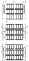
- FIG. 1 is a plan view of a multi-piece substrate according to Embodiment 1.
- FIG. 1 is a flowchart which shows the procedure of the manufacturing method of the multi-piece board
- 6 is a plan view of a multi-piece substrate according to Embodiment 2.
- FIG. 24 is a partially enlarged view of FIG. 23. It is a figure for demonstrating the process of irradiating UV (ultraviolet rays) to an adhesive agent. It is a flowchart which shows the procedure of the manufacturing method of the multi-piece board
- FIG. 31 is a partially enlarged view of FIG. 30. It is a figure for demonstrating the process of joining a 1st frame part and a 1st connection piece unit. It is a figure for demonstrating the external shape processing process after joining a 1st flame
- the multi-piece substrate 10 to be manufactured in the present embodiment includes frame portions 11a and 11b as connecting members and piece portions 12a, 12b, 12c, and 12d as shown in FIG. 1, for example.
- the frame portions 11a and 11b are two elongated rod-like portions sandwiching the continuous piece portions 12a to 12d.
- the piece parts 12a to 12d are connected to each other via frame parts 11a and 11b.
- the shapes of the frame portions 11a and 11b are arbitrary. For example, it may be a parallelogram, circle, or ellipse frame surrounding the piece portions 12a to 12d.
- the frame parts 11a and 11b are made of the same material as the piece parts 12a to 12d, for example. However, this is not essential, and it may be made of a material different from that of the piece portions 12a to 12d. For example, you may manufacture only with an insulating material.
- the frame portions 11a and 11b are manufactured by, for example, a well-known photolithography technique.
- the piece parts 12a to 12d are made of a wiring board.
- the piece portions 12a to 12d are rectangular rigid wiring boards.
- This rigid wiring board includes, for example, a circuit of an electronic device.
- the piece portions 12a to 12d are formed by, for example, a general manufacturing method of a laminated wiring board, for example, uncured epoxy resin, polyimide resin, phenol resin, or the like on a substrate such as glass cloth, aramid fiber nonwoven fabric, or paper It can be manufactured by laminating prepregs impregnated with.
- the structure of the piece portions 12a to 12d is not limited to this.
- the piece parts 12a to 12d may be, for example, a wiring board in which wiring layers and insulating layers are alternately laminated on a ceramic base material.
- the shape of the piece portions 12a to 12d is arbitrary, and may be, for example, a parallelogram, a circle, or an ellipse.
- the piece parts 12a to 12d are not limited to rigid wiring boards.
- a flexible wiring board may be used.
- a flex-rigid wiring board 101 having a flexible portion 101a and rigid portions 101b and 101c as shown in FIG. 2A may be used.
- a wiring board 102 incorporating an electronic component 102a as shown in FIG. 2B may be used.
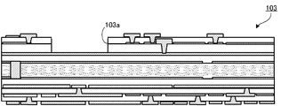
- a wiring board 103 having a cavity 103a formed on the surface thereof may be used.
- these different types of wiring boards may be arbitrarily combined.
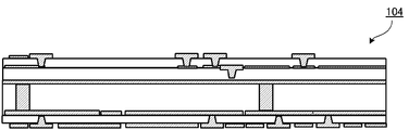
- a low density wiring board 104 as shown in FIG. 3A and a high density wiring board 105 as shown in FIG. 3B may be combined.
- the low density wiring board is a wiring board having a wiring density lower than that of the high density wiring board.
- slits 13a and 13b are formed between the frame parts 11a and 11b and the piece parts 12a to 12d except for the bridges 121a to 121d and 122a to 122d. That is, the frame portion 11a and the piece portions 12a, 12b, 12c, and 12d are connected via the bridges 121a, 121b, 121c, and 121d, respectively. The frame portion 11b and the piece portions 12a, 12b, 12c, and 12d are connected via bridges 122a, 122b, 122c, and 122d, respectively.
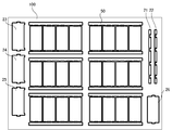
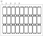
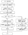
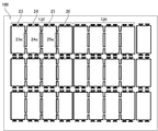
- step S11 the worker makes a multi-piece substrate 10 to be manufactured a plurality of parts, that is, a first portion 21, a second portion 22, a third portion 23, a fourth portion 24, a fifth portion. 5 and the sixth portion 26, as shown in FIG. 5, in the empty space (remainder area) of the manufacturing panel 100 for manufacturing another multi-piece substrate 50, the first to sixth portions are arranged.
- the portions 21 to 26 are laid out.
- the first portion 21 and the second portion 22 substantially correspond to the frame portions 11a and 11b, respectively, and the third portion 23, the fourth portion 24, the fifth portion 25, and the sixth portion 26 are , And generally correspond to the piece portions 12a, 12b, 12c, and 12d, respectively.
- step S12 the worker manufactures the first to sixth portions 21 to 26 on the manufacturing panel 100 according to the above-described layout, for example, by a general build-up process of the laminated wiring board. This step is performed together with the manufacture of the multi-piece substrate 50, for example.
- step S ⁇ b> 13 the operator performs energization inspection on the third portion 23, the fourth portion 24, the fifth portion 25, and the sixth portion 26.
- the part determined to be defective by this energization inspection is repaired or discarded.
- only the portion determined to be non-defective is used. For defective products, good products are replenished from other manufacturing panels, for example.
- step S14 the operator stands the pins 31 in the vicinity of the third portion 23, the fourth portion 24, the fifth portion 25, and the sixth portion 26, respectively.
- the manufacturing panel 100 is fixed.
- the third to sixth portions 23 to 26 are cut out with a normal router machine (router without an alignment function) larger than the external dimensions (design size).
- the cut line is, for example, rectangular.
- the dimensions of this rectangle are set around the third to sixth portions 23 to 26 with a margin with respect to the external dimensions (design size).
- This step is performed together with the cutting of the multi-piece substrate 50, for example.
- the cut line may have a shape other than a rectangular shape, for example, a parallelogram, a circle, an ellipse, or the like.
- step S15 the operator uses the alignment router machine (router having an alignment function) to form the third to sixth parts 23 together with the first and second parts 21 and 22, as shown in FIG. -26 are finished to predetermined external dimensions (design size).
- the alignment router is more accurate than a normal router but is slower to process.
- the outer dimensions of the first and second portions 21 and 22 are set to be thinner than the outer dimensions of the frame portions 11a and 11b.
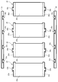
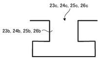
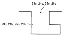
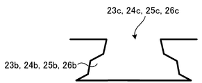
- the first and second portions 21 and 22 have claw receiving portions 23c to 26c at the lower end portion (long side on the piece portion side connected to the bridge). Further, the third to sixth portions 23 to 26 are constituted by body portions 23a to 26a, claws 23b to 26b, and bridge portions 23d to 26d. The claws 23b to 26b and the claw receiving portions 23c to 26c are fitted to each other.
- the trunk portions 23a to 26a are portions corresponding to the piece portions 12a to 12d.
- the claws 23b to 26b are provided on the end surfaces of the body parts 23a to 26a, specifically on the short side facing the frame part.
- the claws 23b to 26b and the body portions 23a to 26a are connected via bridge portions 23d to 26d.
- the claws 23b to 26b are formed of trapezoidal convex portions that expand toward the mating mating claw receiving portions 23c to 26c (frame portions).
- the claw receiving portions 23c to 26c have a shape (the trapezoidal shape) in which the convex portions of the claws 23b to 26b are fitted.
- the bridge portions 23d to 26d are portions including the bridges 121a to 121d and 122a to 122d and the lower end portions (long sides on the piece portion side) of the frame portions 11a and 11b shown in FIG. For this reason, the longitudinal dimensions of the third to sixth portions 23 to 26 are set to be larger than the outer dimensions of the piece portions 12a to 12d.
- the bridge portions 23d to 26d are extended until they are in contact with the adjacent piece portions in order to secure areas for forming the bridges 121a to 121d and 122a to 122d (FIG. 1).
- step S16 the operator combines the first and second parts 21 and 22 and the third to sixth parts 23 to 26. Specifically, as shown in FIG. 8, the operator manually inserts the claws 23b to 26b into the claw receiving portions 23c to 26c. As a result, the first and second portions 21 and 22 and the third to sixth portions 23 to 26 are connected. These are fixed (temporarily fixed) by the frictional force between the claw receiving portions 23c to 26c and the claw 23b to 26b.
- step S17 the operator presses the substrate flat with the manual press machine 301 as shown in FIG.
- the joint portion between the first and second portions 21 and 22 and the third to sixth portions 23 to 26 is flattened.
- the flattening means is arbitrary.
- flattening may be performed using an automatic press machine or a roller press machine.
- workability is improved.
- step S18 the operator inspects the flatness of the substrate with the laser displacement meter 302 as shown in FIG. Subsequently, in step S19, it is determined whether or not the flatness is good. If it is determined in step S19 that the flatness is not good (step S19: NO), the process returns to step S17 and press is performed again.
- step S20 the operator adheres the joint portion using, for example, an adhesive.
- an adhesive for example, after bonding (temporarily fixing) with a photocurable acrylic adhesive, the temporary fixing portion is reinforced with, for example, a thermosetting epoxy adhesive.
- the epoxy adhesive is cured by heat treatment at 100 ° C. for 20 minutes, for example, in an oven.
- the first and second portions 21 and 22 (frame portion) and the third to sixth portions 23 to 26 (piece portions) are also connected by a frictional force caused by fitting. For this reason, as long as sufficient connection strength is obtained, the thermosetting adhesive may not be used, and the two may be bonded (reinforced) only with the non-thermosetting adhesive. If the use of the thermosetting adhesive can be omitted, a change in substrate shape (curing shrinkage, etc.) accompanying a temperature change can be suppressed.
- step S21 the worker forms a slit between the bridge portions 23d to 26d and each piece portion as shown by a broken line in FIG. 11 by a normal router machine (router without an alignment function). To do. As a result, the piece portions 12a to 12d are separated and the slits 13a and 13b and the bridges 121a to 121d and 122a to 122d are formed as shown in FIG. Thus, the multi-piece substrate 10 is manufactured.
- step S22 the operator appropriately corrects the warpage of the substrate.
- step S23 the operator performs an energization inspection on each of the piece portions 12a to 12d. If a defective piece is found by this energization inspection, it is appropriately cut and pasted and replaced with a separately manufactured good piece.
- the multi-piece substrate can be repaired by exchanging the defective piece and the good piece. By performing such repair, when a defect occurs in a part of the multi-piece substrate, it is not necessary to discard the entire substrate, and other good pieces are not wasted. Accordingly, the yield and the number of products can be improved.
- the energization inspection in step S23 may be omitted depending on the application.
- the claws 23b to 26b (second connecting portion) and the claw receiving portions 23c to 26c (first connecting portion) are fitted to each other, so that the frame portions 11a and 11b (first and second connecting portions) are fitted.
- the portions 21 and 22) are connected to the plurality of piece portions 12a to 12d (third to sixth portions 23 to 26). As a result, the piece portions 12a to 12d can be arranged at accurate positions with respect to the frame portions 11a and 11b.
- the first to sixth portions 21 to 26 are laid out in an empty space of the manufacturing panel 100 (one of the manufacturing panels) for manufacturing another multi-piece substrate 50. Then, the first to sixth portions 21 to 26 are manufactured according to the layout. Thus, the yield and the number of products can be improved by effectively utilizing the empty space of the manufacturing panel.
- the above manufacturing method is combined only with those judged to be non-defective products in the inspection process in step S13. Thereby, defective products can be removed in advance.
- the above manufacturing method divides the third to sixth portions 23 to 26 into a plurality of steps (two steps). That is, in step S14, the third to sixth portions 23 to 26 are cut out to be larger than the outer dimension (design size), and then finished to a predetermined outer dimension (design size) by the alignment router in step S15. . Therefore, the dimensional accuracy of the third to sixth portions 23 to 26 is high. In particular, by using an alignment router, the outer shape can be processed with an error level of, for example, ⁇ 20 ⁇ m. Further, since the dimensional accuracy of the joint portion is improved, the accuracy of the alignment between the frame portions 11a and 11b and the piece portions 12a to 12d after connection is also improved.
- the above manufacturing method temporarily fixes the nail receiving portions 23c to 26c and the claws 23b to 26b by fitting them, and therefore does not require a temporary fixing tape or the like. Therefore, no tape fixing process is required. For this reason, manufacturing cost can be reduced.
- the joint portions are flattened after the claw receiving portions 23c to 26c and the claws 23b to 26b are fitted together and before the first and second portions 21 and 22 are bonded with an adhesive. .
- the first and second portions 21 and 22 are bonded to both ends of the third to sixth portions 23 to 26 (piece portions) with an adhesive.
- the temporary fixing portion is reinforced with a thermosetting adhesive (for example, epoxy adhesive).
- a non-thermosetting adhesive for example, acrylic adhesive
- the temporary fixing portion is reinforced with a thermosetting adhesive (for example, epoxy adhesive).
- an adhesive it is possible to bond easily and reliably.
- by temporarily fixing with a non-thermosetting adhesive in advance it is possible to suppress changes in the substrate shape (curing shrinkage, etc.) associated with temperature changes during heat treatment for curing the thermosetting adhesive. it can. Moreover, it can adhere
- the non-thermosetting adhesive is an adhesive that does not require heat treatment for curing, such as a photo-curing adhesive or a two-component curing type.
- a photocurable adhesive is an adhesive that cures upon irradiation with electromagnetic waves such as ultraviolet rays and visible light. In particular, UV curable adhesives and acrylic adhesives are effective.
- the first and second portions 21 and 22 (frame portion) and the third to sixth portions 23 to 26 (piece portions) are not only fitted with the adhesive force but also fitted. It is connected also by the frictional force by. For this reason, as long as sufficient connection strength is obtained, the thermosetting adhesive may not be used, and the two may be bonded (reinforced) only with the non-thermosetting adhesive. If the use of the thermosetting adhesive can be omitted, a change in substrate shape (curing shrinkage, etc.) accompanying a temperature change can be suppressed.
- the outer shapes of the bridges 121a to 121d and 122a to 122d are processed.
- high dimensional accuracy and accuracy can be obtained more easily than when the outer shape is processed before the combination.
- steps S31 to S35 the operator performs the same processing as steps S11 to S15, and, as shown in FIG. 13, the first to second parts 21 and 22 and the third to sixth parts. 23 to 26 are finished to a predetermined external dimension (design size).
- the first and second portions 21 and 22 have claw receiving portions 23c to 26c
- the third to sixth portions 23 to 26 have claws 231b to 261b fitted to the claw receiving portions 23c to 26c.
- the third to sixth portions 23 to 26 further have claw receiving portions 242c to 262c and claws 232b to 252b for connecting adjacent piece portions.
- the claw receiving portions 242c to 262c and the claw 232b to 252b are both formed of convex portions. That is, the claws 232b to 252b are each formed of a trapezoidal convex portion that spreads toward the claw receiving portions 242c to 262c of the mating counterparts (adjacent piece portions).
- the claw receiving portions 242c to 262c are formed as concave portions between the convex portions by disposing two convex portions at a predetermined interval.
- the concave portion has a shape (the trapezoidal shape) in which the convex portions of the claws 232b to 252b are fitted. By fitting these fitting portions to each other, a plurality of adjacent piece portions are connected to each other.
- the third portion 23 has a claw 232b
- the fourth portion 24 arranged next to the claw 232b has a claw receiving portion 242c that fits with the claw 232b, and a claw 242b.
- the fifth portion 25 to be arranged has a claw receiving portion 252c that fits with the claw 242b and a claw 252b
- the sixth portion 26 arranged next to the claw receiving portion 252c fits to the claw 252b. Part 262c.
- step S36 the operator places the first and second portions 21 and 22 on the third to sixth portions 23 to 26, as shown in FIG.
- the sixth parts 23 to 26 are connected to each other.
- the operator manually inserts the claws 23b to 26b into the nail receivers 23c to 26c, and the nails 232b to 252b into the nail receivers 242c to 262c.
- the third to sixth portions 23 to 26 and the first and second portions 21 and 22 are connected, and the third to sixth portions 23 to 26 are connected to each other. These are fixed (temporarily fixed) by the frictional force between the claw receiving portion and the claw.
- steps S37 to S43 (FIG. 12) similar to steps S17 to S23, flattening and bonding of the seam portion, slit processing and separation of the piece portion (broken line in FIG. 14), warp correction, energization inspection, etc. Run to complete the multi-piece substrate 10 (FIG. 1).
- step S41 the slits 13a and 13b (FIG. 1) are formed, and the fitting portions between the claw receiving portions 242c to 262c and the claws 232b to 252b are removed, thereby making the piece portions 12a to 12d (FIG. 1). Separate each other.
- the claws 231b to 261b (second connecting portion) and the claw receiving portions 23c to 26c (first connecting portion) are fitted to each other, whereby the frame portions 11a and 11b (first and second portions) are fitted.
- the portions 21 and 22) are connected to the plurality of piece portions 12a to 12d (third to sixth portions 23 to 26). Further, by fitting the claw receiving portions 242c to 262c (third connecting portion) and the claws 232b to 252b (fourth connecting portion), a plurality of piece portions 12a to 12d (third to sixth portions) 23-26).
- the frame portions 11a and 11b and the piece portions 12a to 12d are joined by filling the clearance (gap) between the connecting portions (the claws and the claw receiving portions) with an adhesive. To do. Prior to joining the frame portions 11a and 11b and the piece portions 12a to 12d, positioning holes are formed in both of them.
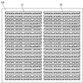
- step S51 the operator separates the third to sixth parts 23 to 26 into the manufacturing panel 100, for example, by a general build-up process of a laminated wiring board, as shown in FIG. Produced in the same state.
- the third portion 23, the fourth portion 24, the fifth portion 25, and the sixth portion 26 generally correspond to the piece portions 12a, 12b, 12c, and 12d (FIG. 1), respectively.
- the third to sixth portions 23 to 26 have the same form.
- step S52 the operator forms a positioning hole (secondary hole 31a) as a through hole as shown in FIG. 17, for example, using an alignment drilling machine.
- the positional accuracy of the secondary hole 31a can be ensured by, for example, forming an alamant mark in, for example, the outermost wiring layer (for example, a conductor pattern made of copper) in step S51. it can.
- the alaminate mark may be exposed by partially removing the protective film or the like during positioning.
- the alamant mark can be optically recognized even through a protective film or the like, it is not necessary to expose the alamant mark.
- step S53 the worker processes the outer shapes of the third to sixth portions 23 to 26 with a normal router machine (router without an alignment function). As a result, the third to sixth portions 23 to 26 are separated from the manufacturing panel 100 as shown in FIG.
- the third portion 23 (or the fourth portion 24, the fifth portion 25, and the sixth portion 26) includes the body portion 23a (or the body portions 24a, 25a, and 26a), It is comprised from the nail
- claw 23b or nail
- bridging part 23d or bridge
- the trunk portion 23a corresponds to the piece portion 12a (FIG. 1)
- the bridge portion 23d corresponds to the bridges 121a and 122a (FIG. 1).
- claw 23b is provided in the end surface of the trunk
- the claw 23b and the body portion 23a are connected via a bridge portion 23d.
- claw 23b consists of a trapezoid-shaped convex part extended toward a front-end
- the claws 23b are formed at, for example, four positions (for example, near the four corners) at the symmetrical position of the body portion 23a.
- the third portion 23 has a point-symmetric form.
- step S54 the operator applies the third to sixth portions 23 to 26 to a checker (electricity inspection apparatus) while keeping the individual pieces, selects only the good pieces, performs acid treatment, and performs an appearance inspection. .
- a checker electricality inspection apparatus
- the operator joins the third to sixth portions 23 to 26 and the first and second portions 21 and 22 in steps S55 and S56.
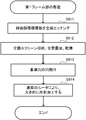
- the first and second parts 21 and 22 are manufactured separately from the third to sixth parts 23 to 26, for example, by an operator executing a series of processes shown in FIG.
- the present invention is not limited to this, and the first and second portions 21 and 22 may be manufactured together on the same manufacturing panel as the third to sixth portions 23 to 26.
- an operator manufactures the first and second portions 21 and 22 on a manufacturing panel 200 different from the manufacturing panel 100 (FIG. 16), for example, as shown in FIG. Specifically, the operator etches the entire manufacturing panel 200 made of the double-sided copper-clad laminate in step S61 of FIG. Subsequently, in step S62, the operator screen prints an insulating material such as an epoxy resin on the entire surface of the manufacturing panel 200, and after the entire surface exposure, the worker dries.
- an insulating material such as an epoxy resin
- step S63 the operator opens a reference hole 31b for positioning as shown in FIG.
- step S62 or step S61
- the positional accuracy of the reference hole 31b can be ensured by forming an alamant mark by patterning or printing a copper foil, for example.
- step S64 the worker processes the outer shape of the first and second portions 21 and 22 with a normal router machine, for example, as shown in FIG. Thereby, the 1st and 2nd parts 21 and 22 are cut off to a predetermined
- the first portion 21 and the second portion 22 generally correspond to the frame portions 11a and 11b (FIG. 1), respectively.
- the first and second portions 21 and 22 have claw receiving portions 23c to 26c at the lower end portion (the long side on the piece portion side connected to the bridge).
- the claw receiving portions 23c to 26c have a shape (the trapezoidal shape) corresponding to the convex portions of the claws 23b to 26b.
- a predetermined clearance (gap) is provided between the claws 23b to 26b and the claw receiving portions 23c to 26c.
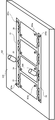
- step S55 of FIG. 15 the operator replaces the first and second portions 21 and 22 with the third to sixth portions 23 to 26, for example, a jig having a pin 303a as shown in FIG. Set to 303.
- an operator inserts the pin 303a into the secondary hole 31a (FIG. 18) and the reference hole 31b (FIG. 22) for positioning.
- the claws 23b to 26b are inserted into the claw receiving portions 23c to 26c (FIG. 22).
- positioning accuracy can be ensured by the pin 303a.
- the worker applies, for example, a UV (ultraviolet) curable adhesive 304 to the first and second portions in step S56. It is applied to the joint between 21 and 22 and the third to sixth portions 23 to 26. Thereby, for example, as shown in FIG. 24 (partially enlarged view of FIG. 23), the adhesive paste 304a is filled in the joint portion.
- the operator causes the first to sixth portions 21 to 26 to flow onto the conveyor-type UV irradiation device 305 while being attached to the jig 303, and applies UV to the adhesive paste 304a. Irradiate.
- the first and second portions 21 and 22 and the third to sixth portions 23 to 26 are joined (adhered).
- step S57 the worker corrects the warp of the substrate. Thereby, the multi-piece substrate 10 as shown in FIG. 1 is completed.
- the frame portions 11a and 11b and the piece portions 12a to 12d are formed by filling the adhesive paste 304a into the clearance (gap) between the claws 23b to 26b and the claw receiving portions 23c to 26c. Join. Therefore, the nails 23b to 26b and the nail receiving portions 23c to 26c can be quickly formed by a simple cutting means such as a normal router, without using an alignment router that requires a long time for processing. Prior to the joining of the two, a positioning hole (secondary hole 31a) is formed prior to the joining of the two. Thereby, both can be positioned with high accuracy. As a result, the number of products obtained per unit time can be improved with rapid outer shape processing.
- the manufacturing method of this embodiment manufactures the piece parts 12a to 12d in a state where the piece parts 12a to 12d are connected to each other.
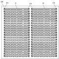
- step S71 the worker connects the third to sixth portions 23 to 26 to the manufacturing panel 100 by a general build-up process of a laminated wiring board, for example, as shown in FIG. Produced in the same state.
- the third portion 23, the fourth portion 24, the fifth portion 25, and the sixth portion 26 generally correspond to the piece portions 12a, 12b, 12c, and 12d (FIG. 1), respectively.
- the third to sixth portions 23 to 26 have the same form.
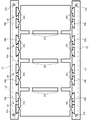
- step S72 the worker processes the outer shape of the connecting piece unit 120 by a normal router machine (router without an alignment function). Thereby, the connection piece unit 120 is cut off from the manufacturing panel 100 as shown in FIG.
- the third to sixth portions 23 to 26 constituting the connection piece unit 120 are basically the same except that the adjacent body portions 23a to 26a are connected to each other by the horizontal connection portions 23e to 25e. It has the same form as the case of Embodiment 3.
- the claws 23b to 26b are fitting claws to be fitted with mating mates (specifically, claw receiving portions 23c to 26c shown in FIG. 30 described later).
- the claws 23b to 26b are formed to have a predetermined outer dimension (design size) by the process of step S72.
- the horizontal connecting portions 23e to 25e are formed in the body portions 23a to 26a by a required number (for example, two for each connecting portion).
- the number of the horizontal connecting portions 23e to 25e is arbitrary.
- step S73 the operator applies the third to sixth portions 23 to 26 to a checker (electricity inspection device), performs acid treatment, and performs an appearance inspection.
- step S74 it is determined whether or not there is a defective piece (defective product) in the third to sixth portions 23 to 26.
- step S74 if it is determined that all are good pieces (step S74: NO), the process proceeds to steps S74 to S77. In other words, in steps S75 and S76, the operator performs the third to sixth portions 23 to 26 and the first and second portions 21 and 22 (first frame portion) of the connection piece unit 120 (first connection piece unit). ).
- a 1st connection piece unit is a connection piece unit which does not contain a defective piece.
- the first frame part is manufactured separately from the connected piece unit 120 by, for example, an operator executing a series of processes shown in FIG.
- the present invention is not limited to this, and the first frame portion may be manufactured together on the same manufacturing panel as the connection piece unit 120.
- the operator first performs the same processing as steps S61 to S63 in FIG. 19 in steps S911 to S913, and as shown in FIG. 21, the manufacturing panel 100 (FIG. 27) and The first and second portions 21 and 22 are manufactured on another manufacturing panel 200, and then the whole surface etching, whole screen printing, whole surface exposure, drying, and drilling of the reference hole 31b are continued.
- step S914 the worker performs external processing of the first and second portions 21 and 22 by using a normal router machine, for example, as shown in FIG.
- a normal router machine for example, as shown in FIG.
- the first and second portions 21 and 22 are larger than a predetermined outer dimension L2 (design size at the time of product shipment). Cut out larger.
- the first portion 21 and the second portion 22 generally correspond to the frame portions 11a and 11b (FIG. 1), respectively. And it has the same form as the case of Embodiment 3 fundamentally. However, the claw receiving portions 23c to 26c are fitted with the claws 23b to 26b (claws larger than the outer dimension L1 in FIG. 28) of the connecting piece unit 120.
- step S75 of FIG. 26 the operator stands a pin in the reference hole 31b and fixes the first and second portions 21 and 22 (first frame portion) to the jig, for example, as shown in FIG.
- the operator holds the claws 23b to 26b of the third to sixth portions 23 to 26 (first connection piece unit) on the claw receiving portions 23c to 26c of the first and second portions 21 and 22. Fit in.
- the claw receiving portions 23c to 26c and the claws 23b to 26b the two are connected by a frictional force.
- step S76 for example, a UV (ultraviolet) curable adhesive is applied and irradiated with UV. Thereby, the junction part of the 1st and 2nd parts 21 and 22 and the connection piece unit 120 is reinforced.
- step S77 the worker processes the first and second portions 21 and 22 and the connecting piece unit 120 by, for example, an alignment router. Specifically, for example, as shown in FIG. 33, the outer shape of the first and second portions 21 and 22 is formed to the outer dimension L2, and the third connecting portion 23e to 25e are removed, The fourth portion 24, the fifth portion 25, and the sixth portion 26 are separated from each other. Thereby, the multi-piece substrate 10 as shown in FIG. 1 is completed.
- step S74 determines whether there is a defective piece.
- step S74 determines whether there is a defective piece.
- the process proceeds to steps S78 to S80.
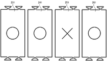
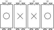
- the third, fourth, and sixth portions 231, 241, 261 determined to be good pieces, and the fifth portion 251 determined to be a defective piece
- the connected piece unit 1201 (second connected piece unit) having the third and sixth parts 232 and 262 determined to be good pieces, as shown in FIG. 34B, and determined to be defective pieces.
- the description will be continued by taking the connecting piece unit 1202 (second connecting piece unit) having the fourth and fifth portions 242 and 252 as an example.
- a 2nd connection piece unit is a connection piece unit containing a defective piece.
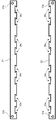
- step S78 of FIG. 26 the worker processes the outer shape of the connection piece units 1201 and 1202 by the alignment router. Specifically, for example, as shown in FIGS. 35A and 35B, the outer shapes of the claws 23b to 26b are formed to have a smaller outer dimension L1 (see FIG. 28), and the lateral coupling portions 23e to 25e are removed, The parts 231 and 232, the fourth parts 241 and 242, the fifth parts 251 and 252, and the sixth parts 261 and 262 are separated from each other. The outer shape processing and separation of the claws 23b to 26b may be performed only on the good pieces.
- the second frame portion is manufactured separately from the connected piece units 1201 and 1202 by, for example, an operator executing a series of processes shown in FIG.
- the present invention is not limited to this, and the second frame portion may be manufactured together on the same manufacturing panel as the second connection piece unit. Further, the second frame part and the first frame part may be manufactured together on a common manufacturing panel.
- the worker first performs the same processing as steps S61 to S63 of FIG. 19 in steps S921 to S923, and as shown in FIG. 21, the manufacturing panel 100 (FIG. 27) and The first and second portions 21 and 22 are manufactured on another manufacturing panel 200, and then the whole surface etching, whole screen printing, whole surface exposure, drying, and drilling of the reference hole 31b are continued.
- step S924 the operator performs external processing of the first and second portions 21 and 22 by a normal router machine, for example, as shown in FIG. Thereby, the 1st and 2nd parts 21 and 22 are cut off by the predetermined
- the first portion 21 and the second portion 22 generally correspond to the frame portions 11a and 11b (FIG. 1), respectively. And it has the same form as the case of Embodiment 3 fundamentally. However, the claw receiving portions 23c to 26c are fitted with the claws 23b to 26b (claws having the outer dimension L1) of the connecting piece units 1201 and 1202.
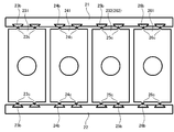
- step S79 of FIG. 26 the operator performs good pieces included in the two second connection piece units, that is, the third, fourth, and sixth portions 231, 241, 261 (connection piece unit 1201), and the third , Any four of the sixth parts 232 and 262 (connection piece unit 1202) are selected. Then, in a state where the pin is set up in the reference hole 31b and the first and second portions 21 and 22 (second frame portion) are fixed to the jig, for example, as shown in FIG. The operator fits the claw 23b to 26b of the good piece into the claw receiving portions 23c to 26c of the portions 21 and 22 by hand. By fitting the claw receiving portions 23c to 26c and the claws 23b to 26b, the two are connected by a frictional force.
- step S80 for example, a UV (ultraviolet) curable adhesive is applied and irradiated with UV. Thereby, the junction part of a 2nd frame part and a good piece is reinforced. Then, the multi-piece substrate 10 as shown in FIG. 1 is completed.
- a UV (ultraviolet) curable adhesive is applied and irradiated with UV.
- the form of the claw receiving portions 23c to 26c (first connection portions) is separately provided for the first connection piece unit that does not include a defective piece and the second connection piece unit that includes a defective piece.
- Different first and second frame portions are prepared. For this reason, it is possible to externally process the claws 23b to 26b (second connection portion) of the first connection piece unit and the claws 23b to 26b (second connection portion) of the second connection piece unit in different modes. In any case, high reliability can be secured for the connection between the frame portion and the piece portion.
- the first connection piece unit is connected to the first and second portions 21 and 22 (frame portion) by separating the second connection piece unit in pieces while the piece portions are connected to each other. .
- the claws 23b to 26b can be quickly processed by simple cutting means such as a normal router. High reliability is obtained for the connection with the frame portion.
- the second connecting piece units are not connected to each other, high positional accuracy cannot be obtained. For this reason, in order to ensure high reliability in connection with the frame portion, it is necessary to perform outline processing with high accuracy by an alignment router or the like that requires a long time for processing.
- the outer shape of the claws 23b to 26b is further processed by the alignment router. Further, the claw 23b to 26b of the first connection piece unit and the claw 23b to 26b of the second connection piece unit are processed into different forms by this additional outer shape processing.
- a first frame part and a second frame part are separately prepared for the first connection piece unit and the second connection piece unit. That is, in any case, a frame portion having claw receiving portions 23c to 26c suitable for the shape of the claw 23b to 26b is prepared.
- the process of preparing the first frame part and the second frame part includes not only the case where materials and parts are purchased and manufactured by itself, but also the case where a finished product is purchased and used.
- the number of products taken per unit time can be improved by reducing the number of times of using an alignment router or the like that requires a long time for processing, such as not using an alignment router before connecting the first connecting piece units.
- all parts of the multi-piece substrate 10 are manufactured in a single manufacturing panel 100. For example, as shown in FIG. You may make it combine them later. By doing so, it becomes easy to combine different types of wiring boards.
- the frame portion and the piece portion of the multi-piece substrate 10 are laid out in the empty space of the manufacturing panel 100 for manufacturing the multi-piece substrate 50.
- the present invention is not limited to this, and the frame portion and the piece portion of the multi-piece substrate 10 are laid out in an empty space of a production panel for producing a substrate other than the multi-piece substrate, for example, a substrate composed of only a single piece. It may be.
- it is not essential to manufacture the frame part or piece part of the multi-piece substrate 10 in an empty space of a manufacturing panel for manufacturing another substrate.
- the frame portion and the piece portion may be manufactured on a manufacturing panel for manufacturing the multi-piece substrate 10.
- the outer shape of the part is divided into two stages, but the outer shape of the part may be divided into three or more stages. Further, the outer shape may be processed once with an alignment router, a normal router bit (router without an alignment function), a laser, or the like. In addition, only the connecting portion may be processed into outer shapes in a plurality of stages.
- a UV curable adhesive was used.
- the kind of adhesive agent is arbitrary.
- other non-thermosetting adhesives may be used.
- a thermosetting adhesive may be used.
- first to fourth connecting portions (claws and claw receiving portions) is arbitrary. As the number of the claws and the nail receiving portions is increased, the bonding force (fixing) becomes stronger, but the manufacture becomes difficult.
- the shapes of the claws 23b to 26b and the claw receiving portions 23c to 26c are not limited to trapezoidal shapes.
- the claws 23b to 26b may be T-shaped or L-shaped.
- the sides of the claws 23b to 26b may be formed in a zigzag shape.
- the shape of the connecting portion is basically arbitrary. However, in order to firmly couple a plurality of parts, it is preferable that when one of the parts is pulled parallel to the main surface of the substrate, the connecting portion is hooked on the other and one of them does not come off from the other.
- the steps of the above embodiment are not limited to the order shown in the flowchart, and the order can be arbitrarily changed without departing from the gist of the present invention. Moreover, you may omit the process which is not required according to a use etc. For example, the step of inspecting flatness can be omitted when strict flatness is not required.
- the material, size, number of layers, etc. of each layer can be arbitrarily changed.
- the method for manufacturing a multi-piece substrate of the present invention is suitable for manufacturing a multi-piece substrate suitable for forming an electric circuit.
Landscapes
- Engineering & Computer Science (AREA)
- Microelectronics & Electronic Packaging (AREA)
- Manufacturing & Machinery (AREA)
- Structure Of Printed Boards (AREA)
- Combinations Of Printed Boards (AREA)
- Measurement Of Radiation (AREA)
Abstract
Description
本実施形態で製造対象とする多ピース基板10は、例えば図1に示すように、連結部材としてのフレーム部11a及び11bと、ピース部12a、12b、12c、12dと、を有する。
本実施形態の製造方法は、フレーム部とピース部とを連結する嵌合部に加えて、ピース部同士をつなぐ嵌合部も形成する。
本実施形態の製造方法は、連結部(爪及び爪受け部)間のクリアランス(隙間)に接着剤を充填することで、フレーム部11a及び11bとピース部12a~12dと(図1)を接合する。また、フレーム部11a及び11bとピース部12a~12dとの接合に先立ち、両者に位置決め用の穴を形成する。
本実施形態の製造方法は、ピース部12a~12dを、それらピース部12a~12d同士が相互に連結された状態で、製造する。
上記実施形態1、2では、多ピース基板10の全パーツを単一の製造パネル100に製造したが、例えば図39に示すように、複数の製造パネル100、200、300に分けて製造し、後でそれらを組み合わせるようにしてもよい。こうすることで、異種配線板の組合せも容易になる。
11a、11b フレーム部
12a~12d ピース部
13a、13b スリット
21~26 第1~第6の部分
23a~26a 胴体部
23b~26b、231b~261b 爪(第2の連結部)
23c~26c 爪受け部(第1の連結部)
23d~26d ブリッジ部
23e~25e 横連結部
31、303a ピン
31a 2次穴
31b 基準穴
50 多ピース基板
100、200、300 製造パネル
101 フレックスリジッド配線板
102 配線板(電子部品を内蔵する配線板)
103 配線板(キャビティが形成された配線板)
104 低密度配線板
105 高密度配線板
120 連結ピースユニット(第1連結ピースユニット)
121a~121d、122a~122d ブリッジ
221a~221d、222a~222d ブリッジ
232b~252b 爪(第4の連結部)
242c~262c 爪受け部(第3の連結部)
301 手動プレス機
302 レーザ変位計
303 治具
304 接着剤
304a 接着剤ペースト
305 コンベア式UV照射装置
1201、1202 連結ピースユニット(第2連結ピースユニット)
Claims (16)
- フレーム部と、配線板からなって前記フレーム部に接続される複数のピース部と、を有する多ピース基板を製造する方法であって、
製造パネルに、第1の連結部を有する前記フレーム部と、第2の連結部を有するピース部を含む前記複数のピース部とを、少なくとも前記フレーム部と前記ピース部とが分離した状態で、製造することと、
前記フレーム部及び前記複数のピース部を、前記製造パネルからそれぞれ切り取ることと、
前記第1の連結部と前記第2の連結部とを連結させることで、前記フレーム部と前記ピース部とを組み合わせることと、
を含む、
ことを特徴とする多ピース基板の製造方法。 - 前記第1の連結部と前記第2の連結部とは相互に嵌合する、
ことを特徴とする請求項1に記載の多ピース基板の製造方法。 - 前記第1の連結部と前記第2の連結部とは、前記第1の連結部と前記第2の連結部との間に充填された接着剤により連結される、
ことを特徴とする請求項1に記載の多ピース基板の製造方法。 - 前記フレーム部及び前記複数のピース部の製造は、
前記フレーム部及び前記ピース部に、アライメントマークを形成し、
前記アライメントマークを基準にして、前記フレーム部及び前記ピース部の所定の位置に、位置決め用の穴を形成し、
前記位置決め用の穴にピンを挿入して、前記フレーム部及び前記ピース部を位置決めし、
前記第1の連結部と第2の連結部とは、前記フレーム部及び前記ピース部が位置決めされた状態で、前記第1の連結部と前記第2の連結部との間に充填された前記接着剤によって連結される、
ことを特徴とする請求項3に記載の多ピース基板の製造方法。 - 前記複数のピース部は、前記複数のピース部同士が連結した状態で製造される、
ことを特徴とする請求項1に記載の多ピース基板の製造方法。 - 前記複数のピース部を有する連結ピースユニットについて、前記ピース部の良否を検査することと、
前記第1の連結部の形態が異なる第1フレーム部及び第2フレーム部を用意することと、
前記検査により不良ピースを含むと判断された第2連結ピースユニットから良ピースを切り取ることと、
をさらに含み、
前記フレーム部と前記ピース部との組み合わせは、
前記第1フレーム部の第1の連結部と、前記検査により不良ピースを含まないと判断された第1連結ピースユニットに含まれる前記ピース部の前記第2の連結部とを連結し、前記第2フレーム部の前記第1の連結部と、前記切り取られた良ピースの前記第2の連結部とを連結する、
ことを特徴とする請求項5に記載の多ピース基板の製造方法。 - 前記第1連結ピースユニットを、第1加工手段により外形加工することと、
前記第2連結ピースユニットを、前記第1加工手段よりも高精度な第2加工手段により外形加工すること、
をさらに含み、
前記良ピースの切り取りは、前記第2加工手段により行い、
前記フレーム部と前記ピース部との組み合わせは、
前記第1フレーム部の前記第1の連結部と、外形加工された前記第1連結ピースユニットに含まれる前記ピース部の前記第2の連結部とを連結し、前記第2フレーム部の前記1連結部と、外形加工された前記良ピースに前記第2フレーム部とを連結する、
ことを特徴とする請求項6に記載の多ピース基板の製造方法。 - 前記第1加工手段はアライメント機能を備えないルータであり、前記第2加工手段はアライメント機能を備えるルータである、
ことを特徴とする請求項7に記載の多ピース基板の製造方法。 - 前記複数のピース部には、第3の連結部を有する第1のピース部と、前記第3の連結部と連結する第4の連結部を有する第2のピース部と、が含まれ、
前記フレーム部と前記ピース部との組み合わせは、前記第1のピース部の前記第3の連結部と、前記第2のピース部の前記第4の連結部とを連結させる、
ことを特徴とする請求項1に記載の多ピース基板の製造方法。 - 前記第3の連結部と前記第4の連結部との連結部分を除去することをさらに含む、
ことを特徴とする請求項9に記載の多ピース基板の製造方法。 - 接着剤により、前記フレーム部と前記ピース部とを接着することをさらに含む、
ことを特徴とする請求項1に記載の多ピース基板の製造方法。 - 前記フレーム部と前記ピース部との接着は、非熱硬化型接着剤により、前記フレーム部と前記ピース部とを仮止めした後、熱硬化型接着剤により、その仮止め部分を補強する、
ことを特徴とする請求項11に記載の多ピース基板の製造方法。 - 製造された前記ピース部について、その良否を検査することをさらに含み、
前記フレーム部と前記ピース部との組み合わせは、前記検査により良ピースであると判断されたもののみを組み合わせる、
ことを特徴とする請求項1に記載の多ピース基板の製造方法。 - 前記製造パネルから切り取ったピース部を、複数の段階に分けて外形加工をすることをさらに含む、
ことを特徴とする請求項1に記載の多ピース基板の製造方法。 - 前記外形加工は、アライメントルータにより行う、
ことを特徴とする請求項14に記載の多ピース基板の製造方法。 - 前記フレーム部と前記ピース部とを接続するブリッジの外形加工をすることをさらに含む、
ことを特徴とする請求項1に記載の多ピース基板の製造方法。
Priority Applications (2)
| Application Number | Priority Date | Filing Date | Title |
|---|---|---|---|
| JP2010536753A JP5079099B2 (ja) | 2008-11-07 | 2009-10-29 | 多ピース基板の製造方法 |
| CN200980144477.4A CN102210198B (zh) | 2008-11-07 | 2009-10-29 | 多片式基板的制造方法 |
Applications Claiming Priority (2)
| Application Number | Priority Date | Filing Date | Title |
|---|---|---|---|
| JP2008-287213 | 2008-11-07 | ||
| JP2008287213 | 2008-11-07 |
Publications (1)
| Publication Number | Publication Date |
|---|---|
| WO2010053046A1 true WO2010053046A1 (ja) | 2010-05-14 |
Family
ID=42152856
Family Applications (1)
| Application Number | Title | Priority Date | Filing Date |
|---|---|---|---|
| PCT/JP2009/068620 Ceased WO2010053046A1 (ja) | 2008-11-07 | 2009-10-29 | 多ピース基板の製造方法 |
Country Status (6)
| Country | Link |
|---|---|
| US (1) | US8572839B2 (ja) |
| JP (1) | JP5079099B2 (ja) |
| KR (1) | KR20110039365A (ja) |
| CN (1) | CN102210198B (ja) |
| TW (1) | TW201029541A (ja) |
| WO (1) | WO2010053046A1 (ja) |
Families Citing this family (10)
| Publication number | Priority date | Publication date | Assignee | Title |
|---|---|---|---|---|
| US8698004B2 (en) * | 2008-10-27 | 2014-04-15 | Ibiden Co., Ltd. | Multi-piece board and fabrication method thereof |
| AT12323U1 (de) * | 2009-03-09 | 2012-03-15 | Austria Tech & System Tech | Verfahren und system zum verbinden einer mehrzahl von leiterplatten mit wenigstens einem rahmen- bzw. trägerelement sowie leiterplatte und rahmen- bzw. trägerelement |
| CN102036487B (zh) * | 2010-11-11 | 2013-11-20 | 北大方正集团有限公司 | 套板成型加工的方法、装置及套板 |
| CN103025056B (zh) * | 2011-09-21 | 2015-08-12 | 揖斐电电子(北京)有限公司 | 多片排版基板及其制造方法 |
| AT13232U1 (de) * | 2011-12-28 | 2013-08-15 | Austria Tech & System Tech | Verfahren zum herstellen einer aus wenigstens zwei leiterplattenbereichen bestehenden leiterplatte sowie leiterplatte |
| KR101518693B1 (ko) * | 2012-08-30 | 2015-05-08 | 이비덴 가부시키가이샤 | 기판 교체 공법, 다피스 기판의 제조 방법, 및 다피스 기판 |
| JP2014096468A (ja) * | 2012-11-09 | 2014-05-22 | Ibiden Co Ltd | 複合配線板及び複合配線板の製造方法 |
| CN104619130B (zh) * | 2013-11-05 | 2018-06-19 | 健鼎(无锡)电子有限公司 | 电路板移植结构以及移植电路板的方法 |
| JP2015097226A (ja) * | 2013-11-15 | 2015-05-21 | イビデン株式会社 | 複合配線板 |
| WO2020217951A1 (ja) * | 2019-04-26 | 2020-10-29 | Tdk株式会社 | 集合基板及びその製造方法 |
Citations (7)
| Publication number | Priority date | Publication date | Assignee | Title |
|---|---|---|---|---|
| JPH07335998A (ja) * | 1994-06-10 | 1995-12-22 | Sony Corp | プリント回路基板及びこのプリント回路基板への部品実装方法 |
| JPH11307905A (ja) * | 1998-04-22 | 1999-11-05 | Sony Corp | 複数面付け基板シート、その再生方法及びそれに用いる位置決め装置 |
| JP2000252605A (ja) * | 1999-02-23 | 2000-09-14 | Samsung Electro Mech Co Ltd | 基板シートの結合方法および装置 |
| JP2002171034A (ja) * | 2000-12-01 | 2002-06-14 | Toshiba Corp | 多面取りプリント基板 |
| JP2002261436A (ja) * | 2001-02-27 | 2002-09-13 | Matsushita Electric Ind Co Ltd | プリント基板の電子部品実装方法と半田付け方法及び連結手段を有するプリント基板 |
| JP2002289986A (ja) * | 2001-03-26 | 2002-10-04 | Ibiden Co Ltd | 多ピース基板およびその製造方法 |
| JP2002353572A (ja) * | 2001-05-25 | 2002-12-06 | Ibiden Co Ltd | 多ピース基板およびその製造方法 |
Family Cites Families (8)
| Publication number | Priority date | Publication date | Assignee | Title |
|---|---|---|---|---|
| DE19600928A1 (de) * | 1996-01-12 | 1997-07-24 | Ibm | Vorrichtung zur Handhabung von Leiterplatten und deren Herstellung |
| JP2002232089A (ja) | 2001-01-30 | 2002-08-16 | Ibiden Denshi Kogyo Kk | 多ピース基板およびその製造方法 |
| US6727591B2 (en) * | 2001-03-26 | 2004-04-27 | Ibiden Co., Ltd. | Multi-piece substrate and method of manufacturing the substrate |
| JP4249918B2 (ja) | 2001-08-30 | 2009-04-08 | イビデン株式会社 | 多ピース基板 |
| TWI228020B (en) | 2003-12-02 | 2005-02-11 | Jin-Chiuan Lai | Method for replacing inter-connected defective printed circuit boards |
| JP2005322878A (ja) | 2004-04-09 | 2005-11-17 | Dainippon Printing Co Ltd | 印刷配線基板の組付パネル、印刷配線基板の実装用単位シート、リジッド−フレキシブル基板及びこれらの製造方法 |
| TW200717208A (en) * | 2005-10-18 | 2007-05-01 | Sheng-San Gu | Defective connected piece of PCB reset method and system thereof |
| JP4923510B2 (ja) | 2005-10-19 | 2012-04-25 | 大日本印刷株式会社 | リジッド−フレキシブル基板及びその製造方法 |
-
2009
- 2009-07-09 US US12/500,041 patent/US8572839B2/en not_active Expired - Fee Related
- 2009-10-29 JP JP2010536753A patent/JP5079099B2/ja not_active Expired - Fee Related
- 2009-10-29 CN CN200980144477.4A patent/CN102210198B/zh not_active Expired - Fee Related
- 2009-10-29 KR KR1020117004835A patent/KR20110039365A/ko not_active Abandoned
- 2009-10-29 WO PCT/JP2009/068620 patent/WO2010053046A1/ja not_active Ceased
- 2009-11-03 TW TW098137287A patent/TW201029541A/zh unknown
Patent Citations (7)
| Publication number | Priority date | Publication date | Assignee | Title |
|---|---|---|---|---|
| JPH07335998A (ja) * | 1994-06-10 | 1995-12-22 | Sony Corp | プリント回路基板及びこのプリント回路基板への部品実装方法 |
| JPH11307905A (ja) * | 1998-04-22 | 1999-11-05 | Sony Corp | 複数面付け基板シート、その再生方法及びそれに用いる位置決め装置 |
| JP2000252605A (ja) * | 1999-02-23 | 2000-09-14 | Samsung Electro Mech Co Ltd | 基板シートの結合方法および装置 |
| JP2002171034A (ja) * | 2000-12-01 | 2002-06-14 | Toshiba Corp | 多面取りプリント基板 |
| JP2002261436A (ja) * | 2001-02-27 | 2002-09-13 | Matsushita Electric Ind Co Ltd | プリント基板の電子部品実装方法と半田付け方法及び連結手段を有するプリント基板 |
| JP2002289986A (ja) * | 2001-03-26 | 2002-10-04 | Ibiden Co Ltd | 多ピース基板およびその製造方法 |
| JP2002353572A (ja) * | 2001-05-25 | 2002-12-06 | Ibiden Co Ltd | 多ピース基板およびその製造方法 |
Also Published As
| Publication number | Publication date |
|---|---|
| KR20110039365A (ko) | 2011-04-15 |
| US8572839B2 (en) | 2013-11-05 |
| US20100115766A1 (en) | 2010-05-13 |
| JPWO2010053046A1 (ja) | 2012-04-05 |
| CN102210198A (zh) | 2011-10-05 |
| TW201029541A (en) | 2010-08-01 |
| JP5079099B2 (ja) | 2012-11-21 |
| CN102210198B (zh) | 2014-12-24 |
Similar Documents
| Publication | Publication Date | Title |
|---|---|---|
| JP5079099B2 (ja) | 多ピース基板の製造方法 | |
| CN101843180B (zh) | 多连片基板及其制造方法 | |
| US8926785B2 (en) | Multi-piece board and method for manufacturing the same | |
| CN102598877B (zh) | 多片基板及其制造方法 | |
| JP4934747B2 (ja) | 多ピース基板及びその製造方法 | |
| JP4934746B2 (ja) | 多ピース基板及びその製造方法 | |
| JP2013080754A (ja) | 多ピース基板の製造方法及び多ピース基板 |
Legal Events
| Date | Code | Title | Description |
|---|---|---|---|
| WWE | Wipo information: entry into national phase |
Ref document number: 200980144477.4 Country of ref document: CN |
|
| 121 | Ep: the epo has been informed by wipo that ep was designated in this application |
Ref document number: 09824746 Country of ref document: EP Kind code of ref document: A1 |
|
| WWE | Wipo information: entry into national phase |
Ref document number: 2010536753 Country of ref document: JP |
|
| ENP | Entry into the national phase |
Ref document number: 20117004835 Country of ref document: KR Kind code of ref document: A |
|
| NENP | Non-entry into the national phase |
Ref country code: DE |
|
| 122 | Ep: pct application non-entry in european phase |
Ref document number: 09824746 Country of ref document: EP Kind code of ref document: A1 |