WO2010041633A1 - シミュレーション方法及びシミュレーション装置 - Google Patents
シミュレーション方法及びシミュレーション装置 Download PDFInfo
- Publication number
- WO2010041633A1 WO2010041633A1 PCT/JP2009/067358 JP2009067358W WO2010041633A1 WO 2010041633 A1 WO2010041633 A1 WO 2010041633A1 JP 2009067358 W JP2009067358 W JP 2009067358W WO 2010041633 A1 WO2010041633 A1 WO 2010041633A1
- Authority
- WO
- WIPO (PCT)
- Prior art keywords
- surface potential
- soi
- bulk
- value
- layer
- Prior art date
Links
Images


Classifications
-
- H—ELECTRICITY
- H01—ELECTRIC ELEMENTS
- H01L—SEMICONDUCTOR DEVICES NOT COVERED BY CLASS H10
- H01L22/00—Testing or measuring during manufacture or treatment; Reliability measurements, i.e. testing of parts without further processing to modify the parts as such; Structural arrangements therefor
-
- G—PHYSICS
- G06—COMPUTING; CALCULATING OR COUNTING
- G06F—ELECTRIC DIGITAL DATA PROCESSING
- G06F30/00—Computer-aided design [CAD]
- G06F30/30—Circuit design
- G06F30/36—Circuit design at the analogue level
- G06F30/367—Design verification, e.g. using simulation, simulation program with integrated circuit emphasis [SPICE], direct methods or relaxation methods
-
- G—PHYSICS
- G01—MEASURING; TESTING
- G01R—MEASURING ELECTRIC VARIABLES; MEASURING MAGNETIC VARIABLES
- G01R31/00—Arrangements for testing electric properties; Arrangements for locating electric faults; Arrangements for electrical testing characterised by what is being tested not provided for elsewhere
- G01R31/26—Testing of individual semiconductor devices
Definitions
- the present invention relates to a simulation method and a simulation apparatus for performing device design and circuit simulation of SOI-MOSFET.
- SOI-MOSFETs that form MOSFETs on SOI (silicon-on-insulator) substrates have been used as techniques for increasing the speed and power consumption of CMOS-LSIs.
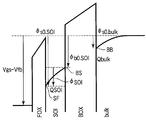
- FIGS. 1A and 1B show cross-sectional configurations of the bulk-MOSFET and the SOI-MOSFET.
- 11 is a semiconductor substrate (also called a bulk in the case of SOI-MOSFET)
- 12 is a buried oxide film (BOX)
- 13 is a silicon layer (SOI layer)
- 14 is A source region, 15 a drain region, 16 a channel region, 17 a gate oxide film (FOX: front-oxide in SOI-MOSFET), and 18 a gate electrode.
- BOX buried oxide film
- FOX gate oxide film
- the stray capacitance is smaller than that of the bulk-MOSFET, so that switching delay can be reduced and leakage current to the semiconductor substrate 11 can also be reduced. it can.
- This SOI-MOSFET is classified into three types, a fully depleted type, a partially depleted type, and a non-completely depleted type, depending on the thickness of the silicon layer (SOI layer).
- the non-fully depleted SOI-MOSFET exhibits characteristics similar to a bulk-MOSFET because the depletion layer in the SOI layer 13 does not reach the buried oxide film 12 under normal voltage conditions.
- the partially depleted SOI-MOSFET only the depletion layer at the drain end of the SOI layer 13 reaches the buried oxide film 12 under normal voltage conditions.
- the fully depleted SOI-MOSFET the entire SOI layer 13 is depleted under normal voltage conditions, and exhibits the most different characteristics from the bulk-MOSFET.
- HiSIM Hiroshima-Univ. STARC IGFET Model
- the operation from the weak inversion to the strong inversion of the MOSFET is derived from the surface potential using a single equation (diffusion-drift equation) to calculate the surface charge and obtain the current.
- diffusion-drift equation a single equation
- the measured values can be reproduced very well by relatively simple calculations.
- the HiSIM is also a bulk-MOSFET model, when it is applied to an SOI-MOSFET, stability and accuracy are reduced.
- SOI-MOSFETs have a large degree of structural freedom, and in order to optimize the structure of SOI-MOSFETs, this equation must be solved stably for all structures. This is because the potential distribution determines the device characteristics. However, it is not easy to solve the Poisson equation stably by iterative calculation.
- the initial solution derivation procedure is as follows (a) to (d).
- the SOI layer is divided into a partially depleted (PD) state or a fully depleted (FD) state, and the analytical solution of the surface potential ⁇ s0.bulk of the bulk layer is determined in each case. Derived for this. This analytical solution is used as an initial solution for the next iterative calculation (c).
- the surface potential ⁇ s0.bulk of the bulk layer is obtained by solving the Newton method (one variable). In solving, the following two Poisson equations of SOI are added together to use equation (1) in which the back surface potential ⁇ b0.SOI of the SOI layer is eliminated.
- the capacitance C SOI of the SOI layer and the surface potential ⁇ s0.bulk of the bulk layer are respectively expressed by the following equations.
- the FD state and the PD state are divided into the FD state if the SOI layer depletion layer width W d.SOI is larger than the SOI layer thickness t SOI , and the PD state if it is smaller.
- the depletion layer width W d.SOI can be expressed by the following equation.
- ⁇ s0.bulk ⁇ s0.bulk_iniA ( ⁇ s0.bulk_iniA ⁇ 2 ⁇ B.bulk )
- ⁇ s0.bulk Smoothing between ⁇ s0.bulk_iniA and ⁇ s0.bulk_iniB ( ⁇ s0.bulk_iniA > 2 ⁇ B.bulk )
- ⁇ s0.bulk_iniA is the initial value of the surface potential when the bulk is depleted
- ⁇ s0.bulk_iniB is the initial value of the surface potential when the bulk is inverted
- ⁇ B.bulk is the difference between the intrinsic Fermi level and the Fermi level. It is a difference.
- a 1 and A 2 are as follows:
- ⁇ s0.bulk_FD_iniB is as follows .
- a 5 and A 6 are respectively represented by the following equations.
- a 7 and A 8 are respectively represented by the following equations.
- ⁇ s0.bulk n + 1 is as follows.
- a bias A may be applied to the substrate as shown in the following equation.
- the simulation is performed with the simulation device using the initial solution obtained as described above and the analytical expression.
- the simulation apparatus includes an input device 21 including, for example, a keyboard, an operation panel, a voice input device, or various data reading devices, a processing device 22 that performs various processes, and a storage device such as a semiconductor memory or a hard disk. 23, and an output device 24 such as a monitor, a printer, and a recording device.
- the processing device 22 includes a control device 22-1 such as a CPU and an arithmetic device 22-2 such as an ALU.
- the control device 22-1 includes an input device 21, an arithmetic device 22-2, a storage device 23, and an output device. Operations such as 24 are controlled.
- a program describing an SOI-MOSFET model parameter stored in the storage device 23, an analytical expression for calculating the SOI layer surface potential ⁇ s0.SOI, and a bulk layer surface potential ⁇ s0.bulk. And a program describing an analytical expression for calculating the potential ⁇ b0.SOI of the back surface of the SOI layer are transferred to the arithmetic unit 22-2 under the control of the control unit 22-1 and described above.
- the initial solution is derived in accordance with the functional equations such as [Equation 1] to [Equation 33].
- the initial solution of the surface potential ⁇ s0.SOI of the SOI layer is derived using the analytical formula of HiSIM2 (STEP 4), and the analytical solution of the surface potential ⁇ s0.bulk of the bulk layer when the SOI layer is in the PD state is derived.
- the analytical solution of the surface potential ⁇ s0.bulk of the bulk layer when the SOI layer is in the PD state is derived.
- an analytical solution of the surface potential ⁇ s0.bulk of the bulk layer when the SOI layer is in the FD state is derived (STEP 6).
- the surface potential ⁇ s0.SOI of the SOI layer obtained in STEP 4 and the bulk layer surface potential ⁇ s0.bulk obtained in STEP 5 and 6 is used as the initial value.
- the surface potential ⁇ s0.bulk of the bulk layer is used. Is obtained by iterative calculation (STEP 7).
- the surface potential ⁇ s0.bulk of the bulk layer obtained in STEP 7 is determined according to a program describing an analytical expression for calculating the potential ⁇ b0.SOI of the back surface of the SOI layer stored in the storage device 23.
- the potential ⁇ b0.SOI on the back surface of the SOI layer is obtained by an analytical expression (STEP 8).
- the surface potential ⁇ s0.SOI (hereinafter referred to as ⁇ 1 ) of the SOI layer as the initial solution and the potential ⁇ of the back surface of the SOI layer in the SOI-MOSFET structure b0.SOI (hereinafter referred to as ⁇ 2 ) and the surface potential ⁇ s0.bulk (hereinafter referred to as ⁇ 3 ) of the bulk layer can be obtained.
- the gate oxide film thickness t FOX , the SOI layer thickness t SOI , the bulk impurity concentration N sub.bulk , the SOI layer impurity concentration N sub.SOI and the like are input from the input device 21.
- Device parameters for SOI-MOSFET, model parameters, and potentials ⁇ 1 , ⁇ 2 , and ⁇ 3 as initial solutions are input and stored in the storage device 23 (STEPs 11 and 12).
- the expressions (A), (B), and (C) are not limited to this, and are expressed by different expressions or different analytical expressions.
- V gp is a value obtained by subtracting the flat band voltage from the gate-source voltage
- Q s0.bulk is the bulk charge amount
- Q n is the inversion charge amount on the SOI surface
- Q dep.SOI is the SOI layer.
- C BOX is the BOX charge capacity
- C FOX is the gate oxide charge capacity.
- C SOI is ⁇ si / t SOI
- ⁇ si is the dielectric constant of silicon
- t SOI is the thickness of the SOI layer.
- the surface potential ⁇ 3 of the bulk layer may be determined. That is, it is attributed to obtaining a solution of simultaneous equations of three variables. In the process of obtaining these solutions by a computer, it is necessary to perform an iterative calculation of three variables by the Newton method.
- STEP14 is executed.
- E is nothing but to make iterative calculation.
- the equation (E) is input from a predetermined input device of the computer system as a three-variable iterative calculation program and stored in the storage device.
- initial values of the surface potential ⁇ 1 of the SOI layer, the potential ⁇ 2 of the back surface of the SOI layer, and the surface potential ⁇ 3 of the bulk layer are input from a predetermined input device of the computer system and stored in the storage device. Let These are stored in an external storage device or the like as a predetermined storage device in the stored program execution type computer system, and loaded into an execution storage device such as a RAM at the time of execution.
- Step 15 16 From STEP11 to STEP14, the iterative calculation program and the initial value at the time of execution of the program are stored in the external storage device or the like, so these are loaded into the RAM or the like at an arbitrary timing and are sequentially or in parallel by the CPU or the like. Can be executed automatically.
- the execution termination condition is when the corrected difference amount ⁇ reaches a predetermined threshold in the calculation process. If the corrected difference amount ⁇ has not reached the threshold value, control is transferred to STEP 13 and the above operation is repeated.
- the SOI layer surface potential ⁇ 1 obtained as the initial value, the back surface potential ⁇ 2 of the SOI layer, and the surface potential ⁇ 3 of the bulk layer are obtained.
- the surface potential ⁇ 1 of the layer, the potential ⁇ 2 of the back surface of the SOI layer, and the surface potential ⁇ 3 of the bulk layer can be obtained.
- STEP 17 In the above STEP 14, when the corrected differential amount ⁇ reaches a threshold value, the potential phi 1, phi 2, device characteristics of the SOI-MOSFET based on phi 3 (solutions of iterative calculation), for example a current, capacity, etc. are determined. Device characteristics refer to the current and capacitance between the gate, source, and drain terminals of the MOSFET, and the current and capacitance between these terminals and the bulk.
- the potential value obtained in the first embodiment can be used as an initial value, and more accurate and multi-variable can be simulated at high speed.
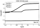
- FIG. 6 is a characteristic diagram showing the relationship between the surface potential of the SOI layer, the back surface potential of the SOI layer, the surface potential of the bulk layer, and the gate-source voltage in a two-dimensional device simulator (2D-Device) model.
- 2D-Device two-dimensional device simulator
- the advantages or effects of HiSIM-SOI over the 2D model are as follows.
- the device structure is divided by a mesh, and Poisson's equation and current continuity equation are connected to each node and numerically solved.
- the amount of calculation inevitably increases, and the number of nodes that can be processed by the computer is limited. Therefore, the 2D device simulator cannot simulate a large-scale circuit, and a circuit simulation of about several transistors is practically limited.
- the calculation time becomes long.
- the device characteristics of the SOI-MOSFET can be simulated stably and with high accuracy. Moreover, since the model has been developed using the structural parameters of the MOSFET, it is possible to easily cope with the difference in structure.
- the SOI-MOSFET can be designed and manufactured by reflecting the MOSFET model and simulation results in the device design and adjusting various device parameters and setting voltages in the MOSFET.
- FIG. 11 shows a third embodiment and shows a method for obtaining circuit characteristics.
- FIG. 12 shows a fourth embodiment and shows a method for specifying device parameters.
- the potentials ⁇ 1 , ⁇ 2 , and ⁇ 3 are calculated according to the flowchart shown in FIG. 5 (STEP 32), and the device characteristics of the SOI-MOSFET, such as the current and capacitance between the terminals, are calculated (STEP 33).
- the device parameter is changed, and the processing of STEPs 31 to 33 is repeated again.
- the device parameters are changed, for example, by changing the gate oxide film thickness, the SOI layer thickness, the bulk impurity concentration, the SOI layer impurity concentration, and the like.
- the calculation process is ended (STEP 35).
- device parameters corresponding to the requested device characteristics can be obtained.
- a simulation method and a simulation apparatus capable of simulating device characteristics of an SOI-MOSFET stably and with high accuracy can be obtained.
- the structure of SOI-MOSFET has a large degree of freedom, the structure can be determined by the simulation of the present invention, and at the same time, the circuit characteristics can be evaluated. For this reason, development cost can be reduced. In addition, the demand for SOI-MOSFETs is great, and the present invention can be applied to various applications.
- the present invention is not limited to the first to fourth embodiments described above, and various modifications can be made without departing from the spirit of the invention.
- the simulation method and the simulation apparatus using only the SOI-MOSFET model have been described as an example.
- a flag is set for calculating the potential required only for the SOI-MOSFET, and the bulk-MOSFET and the SOI- Both MOSFETs can be handled. Therefore, it is possible to simulate a circuit in which bulk-MOSFET and SOI-MOSFET are mixed.
- the first to fourth embodiments include inventions at various stages, and various inventions can be extracted by appropriately combining a plurality of disclosed constituent elements. For example, even if some constituent elements are deleted from all the constituent elements shown in the first to fourth embodiments, at least one of the problems described in the column of problems to be solved by the invention can be solved, and the effect of the invention In the case where at least one of the effects described in the column is obtained, a configuration in which this configuration requirement is deleted can be extracted as an invention.
- the present invention can be applied to device design of SOI-MOSFETs and circuit simulations using SOI-MOSFETs.
Landscapes
- Engineering & Computer Science (AREA)
- Computer Hardware Design (AREA)
- Physics & Mathematics (AREA)
- Theoretical Computer Science (AREA)
- Microelectronics & Electronic Packaging (AREA)
- General Physics & Mathematics (AREA)
- Evolutionary Computation (AREA)
- Geometry (AREA)
- General Engineering & Computer Science (AREA)
- Manufacturing & Machinery (AREA)
- Power Engineering (AREA)
- Thin Film Transistor (AREA)
Priority Applications (5)
| Application Number | Priority Date | Filing Date | Title |
|---|---|---|---|
| KR1020117007942A KR101213268B1 (ko) | 2008-10-06 | 2009-10-05 | 시뮬레이션 방법 및 시뮬레이션 장치 |
| EP09819167A EP2337080A4 (en) | 2008-10-06 | 2009-10-05 | SIMULATION PROCESS AND SIMULATION DEVICE |
| CN2009801393202A CN102171834B (zh) | 2008-10-06 | 2009-10-05 | 模拟方法及模拟装置 |
| JP2010532909A JP5504506B2 (ja) | 2008-10-06 | 2009-10-05 | シミュレーション方法及びシミュレーション装置 |
| US13/080,154 US8731893B2 (en) | 2008-10-06 | 2011-04-05 | Circuit simulation of MOSFETs |
Applications Claiming Priority (2)
| Application Number | Priority Date | Filing Date | Title |
|---|---|---|---|
| JP2008259755 | 2008-10-06 | ||
| JP2008-259755 | 2008-10-06 |
Related Child Applications (1)
| Application Number | Title | Priority Date | Filing Date |
|---|---|---|---|
| US13/080,154 Continuation US8731893B2 (en) | 2008-10-06 | 2011-04-05 | Circuit simulation of MOSFETs |
Publications (1)
| Publication Number | Publication Date |
|---|---|
| WO2010041633A1 true WO2010041633A1 (ja) | 2010-04-15 |
Family
ID=42100583
Family Applications (1)
| Application Number | Title | Priority Date | Filing Date |
|---|---|---|---|
| PCT/JP2009/067358 WO2010041633A1 (ja) | 2008-10-06 | 2009-10-05 | シミュレーション方法及びシミュレーション装置 |
Country Status (6)
| Country | Link |
|---|---|
| US (1) | US8731893B2 (ko) |
| EP (1) | EP2337080A4 (ko) |
| JP (1) | JP5504506B2 (ko) |
| KR (1) | KR101213268B1 (ko) |
| CN (1) | CN102171834B (ko) |
| WO (1) | WO2010041633A1 (ko) |
Families Citing this family (7)
| Publication number | Priority date | Publication date | Assignee | Title |
|---|---|---|---|---|
| JP5405054B2 (ja) * | 2008-06-18 | 2014-02-05 | ルネサスエレクトロニクス株式会社 | 半導体装置の解析及び設計装置、及び半導体装置の解析及び設計方法 |
| CN101976283B (zh) * | 2010-10-21 | 2012-12-19 | 中国科学院上海微系统与信息技术研究所 | Bsimsoi4直流模型参数的确定方法 |
| US9996650B2 (en) | 2015-03-17 | 2018-06-12 | International Business Machines Corporation | Modeling the performance of a field effect transistor having a dynamically depleted channel region |
| JP2018010896A (ja) * | 2016-07-11 | 2018-01-18 | 株式会社村田製作所 | ヘテロ接合バイポーラトランジスタ |
| CN111209675B (zh) * | 2020-01-10 | 2023-04-28 | 南方电网科学研究院有限责任公司 | 电力电子器件的仿真方法、装置、终端设备及存储介质 |
| CN112131792B (zh) * | 2020-09-24 | 2024-06-04 | 南方电网科学研究院有限责任公司 | 一种地表电位还原方法、装置、设备及存储介质 |
| TW202247463A (zh) * | 2021-02-01 | 2022-12-01 | 美商應用材料股份有限公司 | 具全空乏矽晶絕緣體之環繞式閘極元件 |
Family Cites Families (10)
| Publication number | Priority date | Publication date | Assignee | Title |
|---|---|---|---|---|
| US7240021B1 (en) * | 1998-03-27 | 2007-07-03 | Walker Digital, Llc | System and method for tracking and establishing a progressive discount based upon a customer's visits to a retail establishment |
| US20020082920A1 (en) * | 2000-11-17 | 2002-06-27 | Kermit Austin | System and methods for providing a multi-merchant loyalty program |
| US20020111859A1 (en) * | 2001-02-15 | 2002-08-15 | Gregory Sheldon | Integrated frequency and award redemption program for installment based receivables behavior modification and customer loyalty management |
| US20020174011A1 (en) * | 2001-03-14 | 2002-11-21 | Sanchez Michael F. | Systems and methods for conducting a loyalty program |
| JP2004179502A (ja) * | 2002-11-28 | 2004-06-24 | Seiko Epson Corp | 部分空乏型のsoimosfetのspiceパラメータ抽出、spice計算及びデバイス解析の方法 |
| JP4445734B2 (ja) * | 2003-09-10 | 2010-04-07 | 株式会社半導体理工学研究センター | 半導体装置設計用シミュレーション方法、半導体装置設計用シミュレーション装置、ならびに半導体装置およびその製造方法 |
| JP2005259778A (ja) * | 2004-03-09 | 2005-09-22 | Matsushita Electric Ind Co Ltd | 半導体装置の信頼性シミュレーション方法 |
| JP5020562B2 (ja) * | 2006-07-25 | 2012-09-05 | 株式会社 液晶先端技術開発センター | シミュレーション装置、シミュレーション方法、及び半導体装置の製造方法 |
| CN101110092B (zh) * | 2007-08-31 | 2012-03-21 | 上海集成电路研发中心有限公司 | 高压mos晶体管电路仿真宏模型 |
| JP4792439B2 (ja) * | 2007-09-12 | 2011-10-12 | 株式会社半導体理工学研究センター | シミュレーション方法及びシミュレーション装置 |
-
2009
- 2009-10-05 KR KR1020117007942A patent/KR101213268B1/ko not_active IP Right Cessation
- 2009-10-05 WO PCT/JP2009/067358 patent/WO2010041633A1/ja active Application Filing
- 2009-10-05 EP EP09819167A patent/EP2337080A4/en not_active Withdrawn
- 2009-10-05 CN CN2009801393202A patent/CN102171834B/zh not_active Expired - Fee Related
- 2009-10-05 JP JP2010532909A patent/JP5504506B2/ja not_active Expired - Fee Related
-
2011
- 2011-04-05 US US13/080,154 patent/US8731893B2/en not_active Expired - Fee Related
Non-Patent Citations (6)
| Title |
|---|
| M. MIURA-MATTAUSCH, N. SADACHIKA, D. NAVARRO, G. SUZUKI, Y. TAKEDA, M. MIYAKE, T. WARABINO, Y. MIZUKANE, R. INAGAKI, T. EZAKI: "HiSIM2: Advanced MOSFET Model Valid for RF Circuit Simulation", IEEE TRANS. ELECTRON DEVICES, vol. 53, 2006, pages 1994 |
| N. SADACHIKA ET AL.: "Completely Surface- Potential-Based Compact Model of the Fully Depleted SOI-MOSFET Including Short-Channel Effect", IEEE TRANSACTIONS ON ELECOTRON DEVICES, vol. 53, no. 9, September 2006 (2006-09-01), pages 2017 - 2024, XP008149343 * |
| S. VEERATOGHAVAN, J.G. FOGSUM: "A physical short-channel model for the thin-film SOI MOSFET applicable to the device and circuit CAD", IEEE TRANS. ELECTRON DEVICES, vol. 35, no. 11, November 1988 (1988-11-01), pages 1866 - 1875 |
| SAMUEL K.H. FUNG, PIN SU, CHENMING HU: "Present Status and Future Direction of BSIM SOI Model for High-Performance/Low-Power/RF Application", PROC. MODEL. SIMUL. MICROSYSST, 2002, pages 690 - 693 |
| See also references of EP2337080A4 * |
| TAKAHIRO MURAKAMI ET AL.: "SOI-MOSFET ni Okeru Kiban Fuyu Koka no Model-ka", IEICE TECHNICAL REPORT SDM, vol. 107, no. 298, 24 October 2007 (2007-10-24), pages 41 - 45, XP008149896 * |
Also Published As
| Publication number | Publication date |
|---|---|
| EP2337080A4 (en) | 2013-03-20 |
| JPWO2010041633A1 (ja) | 2012-03-08 |
| CN102171834B (zh) | 2013-11-13 |
| KR20110060924A (ko) | 2011-06-08 |
| US8731893B2 (en) | 2014-05-20 |
| KR101213268B1 (ko) | 2012-12-18 |
| EP2337080A1 (en) | 2011-06-22 |
| US20110184708A1 (en) | 2011-07-28 |
| CN102171834A (zh) | 2011-08-31 |
| JP5504506B2 (ja) | 2014-05-28 |
Similar Documents
| Publication | Publication Date | Title |
|---|---|---|
| JP5504506B2 (ja) | シミュレーション方法及びシミュレーション装置 | |
| US7685543B2 (en) | Simulation apparatus and simulation method used to design characteristics and circuits of semiconductor device, and semiconductor device fabrication method | |
| US7730433B2 (en) | Analog design retargeting | |
| US20100257493A1 (en) | Effective gate length circuit modeling based on concurrent length and mobility analysis | |
| JP3269459B2 (ja) | Misfetのオーバラップ長の測定方法、測定装置、抽出プログラムを記録した記録媒体 | |
| Akturk et al. | Compact modeling of 0.35 μm SOI CMOS technology node for 4 K DC operation using Verilog-A | |
| KR101105273B1 (ko) | 비정질 산화물 반도체 박막 트랜지스터의 전류 모델링 방법 및 그 장치 | |
| KR20130010518A (ko) | 비정질 산화물 반도체 박막 트랜지스터의 커패시턴스 모델링 방법 및 그 장치 | |
| US8849643B2 (en) | Table-lookup-based models for yield analysis acceleration | |
| He et al. | BSIM5: An advanced charge-based MOSFET model for nanoscale VLSI circuit simulation | |
| JP2005259778A (ja) | 半導体装置の信頼性シミュレーション方法 | |
| Shamsir et al. | Semiconductor device modeling and simulation for electronic circuit design | |
| Al-Hertani et al. | UDSM subthreshold leakage model for NMOS transistor stacks | |
| Li | A two-dimensional thin-film transistor simulation using adaptive computing technique | |
| US8949083B2 (en) | Modeling gate transconductance in a sub-circuit transistor model | |
| WO2020093525A1 (zh) | 一种半导体器件的等效模型建立方法、装置及终端设备 | |
| Kimura et al. | Table look-up model of thin-film transistors for circuit simulation using spline interpolation with transformation by y= x+ log (x) | |
| JP2011215749A (ja) | 半導体装置設計支援方法、半導体装置設計支援プログラム、及び半導体装置設計支援装置 | |
| Al-Hertani et al. | A new subthreshold leakage model for NMOS transistor stacks | |
| US10777638B1 (en) | Constricted junctionless FinFET/nanowire/nanosheet device having cascode portion | |
| US20120212504A1 (en) | Method and system for extracting compact models for circuit simulation | |
| CN118133753A (zh) | 用于晶体管设计的仿真的参数校准 | |
| Chen et al. | Finite-point-based transistor model: A new approach to fast circuit simulation | |
| Nassar et al. | A Charge-Based Compact Model for Thin-Film Monocrystalline Silicon on Glass PMOSFETs Operated in Accumulation | |
| He et al. | A continuous surface-potential solution from accumulation to inversion for intrinsic symmetric double-gate MOSFETs |
Legal Events
| Date | Code | Title | Description |
|---|---|---|---|
| WWE | Wipo information: entry into national phase |
Ref document number: 200980139320.2 Country of ref document: CN |
|
| 121 | Ep: the epo has been informed by wipo that ep was designated in this application |
Ref document number: 09819167 Country of ref document: EP Kind code of ref document: A1 |
|
| WWE | Wipo information: entry into national phase |
Ref document number: 2010532909 Country of ref document: JP |
|
| WWE | Wipo information: entry into national phase |
Ref document number: 2009819167 Country of ref document: EP |
|
| ENP | Entry into the national phase |
Ref document number: 20117007942 Country of ref document: KR Kind code of ref document: A |
|
| NENP | Non-entry into the national phase |
Ref country code: DE |