WO2010041633A1 - Method of simulation and simulation device - Google Patents
Method of simulation and simulation device Download PDFInfo
- Publication number
- WO2010041633A1 WO2010041633A1 PCT/JP2009/067358 JP2009067358W WO2010041633A1 WO 2010041633 A1 WO2010041633 A1 WO 2010041633A1 JP 2009067358 W JP2009067358 W JP 2009067358W WO 2010041633 A1 WO2010041633 A1 WO 2010041633A1
- Authority
- WO
- WIPO (PCT)
- Prior art keywords
- surface potential
- soi
- bulk
- value
- layer
- Prior art date
Links
Images


Classifications
-
- H—ELECTRICITY
- H01—ELECTRIC ELEMENTS
- H01L—SEMICONDUCTOR DEVICES NOT COVERED BY CLASS H10
- H01L22/00—Testing or measuring during manufacture or treatment; Reliability measurements, i.e. testing of parts without further processing to modify the parts as such; Structural arrangements therefor
-
- G—PHYSICS
- G06—COMPUTING; CALCULATING OR COUNTING
- G06F—ELECTRIC DIGITAL DATA PROCESSING
- G06F30/00—Computer-aided design [CAD]
- G06F30/30—Circuit design
- G06F30/36—Circuit design at the analogue level
- G06F30/367—Design verification, e.g. using simulation, simulation program with integrated circuit emphasis [SPICE], direct methods or relaxation methods
-
- G—PHYSICS
- G01—MEASURING; TESTING
- G01R—MEASURING ELECTRIC VARIABLES; MEASURING MAGNETIC VARIABLES
- G01R31/00—Arrangements for testing electric properties; Arrangements for locating electric faults; Arrangements for electrical testing characterised by what is being tested not provided for elsewhere
- G01R31/26—Testing of individual semiconductor devices
Landscapes
- Engineering & Computer Science (AREA)
- Computer Hardware Design (AREA)
- Physics & Mathematics (AREA)
- Theoretical Computer Science (AREA)
- Microelectronics & Electronic Packaging (AREA)
- General Physics & Mathematics (AREA)
- Evolutionary Computation (AREA)
- Geometry (AREA)
- General Engineering & Computer Science (AREA)
- Manufacturing & Machinery (AREA)
- Power Engineering (AREA)
- Thin Film Transistor (AREA)
Abstract
Description
まず、本発明で用いるSOI-MOSFETモデルの概要とこのモデルに至る考察の課程について説明し、その後、このSOI-MOSFETモデルを用いた本実施形態に係るシミュレーション方法とシミュレーション装置について説明する。 Embodiments of the present invention will be described below with reference to the drawings.
First, an outline of an SOI-MOSFET model used in the present invention and a course of consideration leading to this model will be described, and then a simulation method and a simulation apparatus according to the present embodiment using this SOI-MOSFET model will be described.


φs0.bulk=φs0.bulk_iniAとφs0.bulk_iniBのスムージング(φs0.bulk_iniA>2ΨB.bulk)
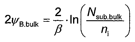
ここで、φs0.bulk_iniAはバルクが空乏状態の表面ポテンシャルの初期値、φs0.bulk_iniBはバルクが反転状態の表面ポテンシャルの初期値、ΨB.bulkは真性フェルミ準位とフェルミ準位との差である。 φ s0.bulk = φ s0.bulk_iniA (φ s0.bulk_iniA <2Ψ B.bulk )
φ s0.bulk = Smoothing between φ s0.bulk_iniA and φ s0.bulk_iniB (φ s0.bulk_iniA > 2Ψ B.bulk )
Where φ s0.bulk_iniA is the initial value of the surface potential when the bulk is depleted, φ s0.bulk_iniB is the initial value of the surface potential when the bulk is inverted, and Ψ B.bulk is the difference between the intrinsic Fermi level and the Fermi level. It is a difference.
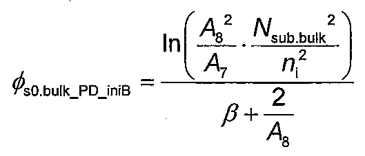
(I.A)FD状態でバルクが空乏状態の場合
バルクに誘起される電荷Qs0.bulkを次式であると近似して式(1)を解く。

(IA) When the bulk is depleted in the FD state, the charge Q s0.bulk induced in the bulk is approximated to the following equation and Equation (1) is solved.
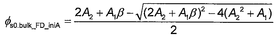


バルクに誘起される電荷Qs0.bulkを次式と近似して式(1)を解く。


PD状態では、SOI層の表面ポテンシャルφs0.SOIが増加すると空乏層が広がっていき次の関係が成立している。
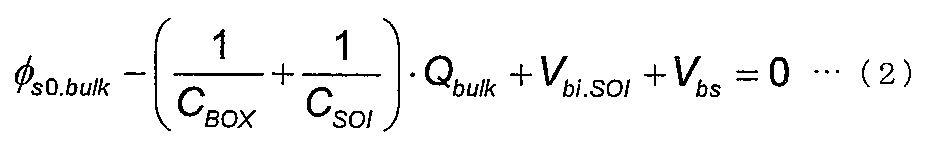


式(2)を次式と近似して解く。


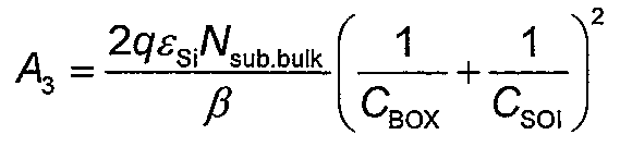
(2.1)FD状態の場合
式(1)より、f(φs0.bulk)を次式として、ニュートン法によりバルク層の表面ポテンシャルφs0.bulkを更新していく。

(2.1) In the case of the FD state From the equation (1), the surface potential φ s0.bulk of the bulk layer is updated by the Newton method using f (φ s0.bulk ) as the following equation.
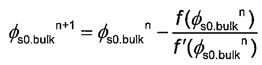
式(2)より、f(φs0.bulk)を次式として、ニュートン法によりバルク層の表面ポテンシャルφs0.bulkを更新していく。


上述したニュートン法で求めたバルク層の表面ポテンシャルφs0.bulkを用いて、次式によりSOI層の表面ポテンシャルφs0.SOIを次式のように導出できる。

Using surface potential φ s0.bulk of the bulk layer obtained by the above-described Newton's method can be derived surface potential phi S0.SOI the SOI layer as follows from the following equation.
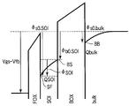
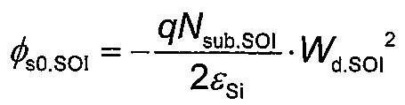
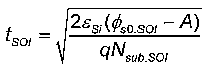
SOI層の空乏層幅Wd.SOIがSOI層の厚さtSOIに到達すると、SOI層表面の反転が早まる。FDになった後にバルクに誘起される電荷Qs0.bulkは、BOXがなければ生じるはずだった空乏電荷「-qNsub.SOI・(Wd.SOI-tSOI)」と比べ無視できるくらい小さいので、ここでは無視すると、空乏層幅がSOI層の厚さtSOIに固定されたbulk-MOSFETと同じようなポテンシャル変化を示すと考えられる。 <Correction of the surface potential φ s0.SOI of the SOI layer when the FD state is reached>
When the depletion layer width W d.SOI of the SOI layer reaches the thickness t SOI of the SOI layer, inversion of the SOI layer surface is accelerated. The charge Q s0.bulk induced in the bulk after becoming FD is negligibly small compared to the depletion charge “−qN sub.SOI · (W d.SOI −t SOI )” that should have been generated without BOX. Therefore, if neglected here, it is considered that the potential change is similar to that of the bulk-MOSFET in which the depletion layer width is fixed to the thickness t SOI of the SOI layer.


次に、上記SOI-MOSFETモデルを用いた、本発明の第1の実施形態に係るシミュレーション方法とシミュレーション装置について図3及び図4により説明する。図3は本発明の実施形態に係るシミュレーション装置の概略構成を示すブロック図、図4は本発明の実施形態に係るシミュレーション方法を示すフローチャートである。 [First Embodiment]
Next, a simulation method and a simulation apparatus according to the first embodiment of the present invention using the SOI-MOSFET model will be described with reference to FIGS. FIG. 3 is a block diagram showing a schematic configuration of a simulation apparatus according to the embodiment of the present invention, and FIG. 4 is a flowchart showing a simulation method according to the embodiment of the present invention.
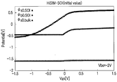
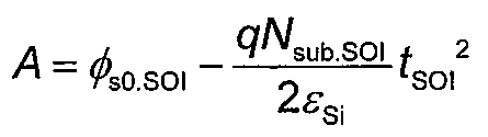
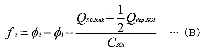
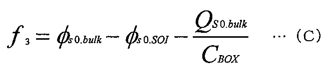
上記第1の実施形態で説明したHiSIM-SOIによるシミュレーション方法により、SOI-MOSFET構造における、初期解であるSOI層の表面ポテンシャルφs0.SOI(以下φ1)と、SOI層の裏面のポテンシャルφb0.SOI(以下φ2)と、バルク層の表面ポテンシャルφs0.bulk(以下φ3)を求めることができる。 [Second Embodiment]
By the simulation method using HiSIM-SOI described in the first embodiment, the surface potential φ s0.SOI (hereinafter referred to as φ 1 ) of the SOI layer as the initial solution and the potential φ of the back surface of the SOI layer in the SOI-MOSFET structure b0.SOI (hereinafter referred to as φ 2 ) and the surface potential φ s0.bulk (hereinafter referred to as φ 3 ) of the bulk layer can be obtained.
の表面ポテンシャルφ3にはそれぞれ、例えば次式(A)、(B)、(C)に例示するような解析式の関係が成り立っていると仮定する。 For the surface potential φ 1 of the SOI layer, the potential φ 2 of the back surface of the SOI layer, and the surface potential φ 3 of the bulk layer, for example, analytical expressions as exemplified in the following formulas (A), (B), and (C), respectively. It is assumed that the following relationship holds.


STEP11からSTEP14により、反復計算のプログラムと当該プラグラム実行時における初期値が外部記憶装置等に記憶されているので、これらを任意のタイミングで、RAM等にロードし、それをCPU等により逐次ないし並列的に実行すればよい。ここで、実行の終了条件は、計算過程において修正差分量δφが所定の閾値に至った場合である。修正差分量δφが閾値に達していない場合、制御がSTEP13に移行され、上記動作が繰り返される。 (
From STEP11 to STEP14, the iterative calculation program and the initial value at the time of execution of the program are stored in the external storage device or the like, so these are loaded into the RAM or the like at an arbitrary timing and are sequentially or in parallel by the CPU or the like. Can be executed automatically. Here, the execution termination condition is when the corrected difference amount δφ reaches a predetermined threshold in the calculation process. If the corrected difference amount δφ has not reached the threshold value, control is transferred to STEP 13 and the above operation is repeated.
上記STEP14において、修正差分量δφが閾値に達した場合、ポテンシャルφ1、φ2、φ3(反復計算の解)に基づきSOI-MOSFETのデバイス特性、例えば電流、容量等が求められる。デバイス特性とは、MOSFETのゲート・ソース及びドレイン端子間の電流及び容量、さらにこれら端子とバルク間の電流及び容量をいう。 (STEP 17)
In the
本発明は、デバイスパラメータに加えて、回路図及び回路の駆動条件を入力装置21より入力して記憶装置23に記憶させ、この記憶装置23に記憶されたデータを利用して回路特性を求めることができる。 [Third Embodiment]
In the present invention, in addition to the device parameters, a circuit diagram and circuit driving conditions are input from the
本発明は、入力するデバイスパラメータを所定のアルゴリズムで変化させ、その計算結果であるデバイス特性が要求されたデバイス特性に一致したとき、計算を終了させることにより、デバイスパラメータを特定することも可能である。 [Fourth Embodiment]
In the present invention, it is also possible to specify a device parameter by changing the input device parameter with a predetermined algorithm and terminating the calculation when the calculated device characteristic matches the requested device characteristic. is there.
Claims (10)
- 埋め込み酸化膜上のシリコン層中にソース領域及びドレイン領域を離隔して形成し、これらソース、ドレイン領域間のチャネル領域上にゲート絶縁膜を介在してゲート電極を形成したトランジスタのデバイス特性をシミュレートするシミュレーション方法において、
前記トランジスタの特性を示すデータの一表現形式である数式を入力装置から入力して記憶装置に記憶させるステップと、
前記トランジスタのデバイスパラメータを前記入力装置から入力して前記記憶装置に記憶させるステップと、
前記記憶装置に記憶した数式とデバイスパラメータとに基づいて演算装置で演算を行って、前記シリコン層における表面ポテンシャルの第1の値を算出するステップと、
前記記憶装置に記憶した数式とデバイスパラメータに基づいて前記演算装置で演算を行って、前記シリコン層が部分空乏状態にあるとき及び前記シリコン層が完全空乏状態にあるときの前記埋め込み酸化膜下におけるバルク層の表面ポテンシャルの第1の値をそれぞれ算出するステップと、
算出した前記シリコン層における表面ポテンシャルの第1の値と、算出した前記バルク層における表面ポテンシャルの第1の値と、前記記憶装置に記憶した数式とに基づいて前記演算装置で演算を行い、前記バルク層における表面ポテンシャルの第2の値を反復計算によって求めるステップと、
前記反復計算によって求めたバルク層における表面ポテンシャルの第2の値と、前記記憶装置に記憶した数式とに基づいて前記演算装置で演算を行い、前記シリコン層における裏面のポテンシャルの第1の値を算出するステップとを具備することを特徴とするシミュレーション方法。 Simulate the device characteristics of a transistor in which a source region and a drain region are formed separately in a silicon layer on a buried oxide film, and a gate electrode is formed on a channel region between the source and drain regions with a gate insulating film interposed therebetween. In the simulation method to
Inputting a mathematical expression, which is an expression form of data indicating the characteristics of the transistor, from an input device and storing it in a storage device;
Inputting device parameters of the transistor from the input device and storing them in the storage device;
Calculating a first value of a surface potential in the silicon layer by performing an operation in an arithmetic device based on the mathematical formula and the device parameter stored in the storage device;
Based on the mathematical formula and device parameters stored in the storage device, the arithmetic unit performs an operation, and when the silicon layer is in a partially depleted state and under the buried oxide film when the silicon layer is in a fully depleted state Respectively calculating a first value of the surface potential of the bulk layer;
Based on the calculated first value of the surface potential in the silicon layer, the calculated first value of the surface potential in the bulk layer, and the mathematical formula stored in the storage device, the calculation device performs the calculation, Obtaining a second value of the surface potential in the bulk layer by iterative calculation;
Based on the second value of the surface potential in the bulk layer obtained by the iterative calculation and the mathematical formula stored in the storage device, the arithmetic device performs an operation, and the first value of the back surface potential in the silicon layer is obtained. And a calculating step. - 前記トランジスタの特性を示すデータの一表現形式であって、前記シリコン層における表面ポテンシャルと、前記バルク層における表面ポテンシャルと、前記シリコン層における裏面のポテンシャルの関係を記述した互いに異なる第1乃至第3の数式を前記入力装置から入力して前記記憶装置に記憶させるステップと、
前記シリコン層における表面ポテンシャルの第1の値と、前記バルク層における表面ポテンシャルの第2の値と、前記シリコン層における裏面のポテンシャルの第1の値とを前記記憶装置に記憶させるステップと、
前記記憶装置に記憶させた、前記互いに異なる第1乃至第3の数式と、前記シリコン層における表面ポテンシャルの第1の値と、前記バルク層における表面ポテンシャルの第2の値と、
前記シリコン層における裏面のポテンシャルの第1の値とに基づいて、前記演算装置で反復演算を行い、前記シリコン層における表面ポテンシャルの第2の値と、前記バルク層における表面ポテンシャルの第3の値と、前記シリコン層における裏面のポテンシャルの第2の値を算出するステップとを更に具備することを特徴とする請求項1記載のシミュレーション方法。 1 is a representation format of data indicating the characteristics of the transistor, and is a first to a third different from each other describing a relationship between a surface potential of the silicon layer, a surface potential of the bulk layer, and a potential of a back surface of the silicon layer. And inputting the mathematical formula from the input device and storing it in the storage device;
Storing the first value of the surface potential in the silicon layer, the second value of the surface potential in the bulk layer, and the first value of the back surface potential in the silicon layer in the storage device;
The different first to third mathematical expressions stored in the storage device, a first value of a surface potential in the silicon layer, and a second value of a surface potential in the bulk layer,
Based on the first value of the potential of the back surface of the silicon layer, the arithmetic device performs an iterative calculation, and the second value of the surface potential of the silicon layer and the third value of the surface potential of the bulk layer. The simulation method according to claim 1, further comprising the step of calculating a second value of the potential of the back surface of the silicon layer. - 前記反復計算において、前記互いに異なる第1乃至第3の数式をヤコビアン行列の数式として前記演算装置で反復演算ステップによりを行うことを特徴とする請求項2記載のシミュレーション方法。 3. The simulation method according to claim 2, wherein, in the iterative calculation, the first to third formulas different from each other are used as formulas of a Jacobian matrix and the calculation unit performs an iterative calculation step.
- 前記シリコン層における表面ポテンシャルの第1の値の算出は、表面ポテンシャルに基づくbulk-MOSFETモデルを用いて行うことを特徴とする請求項1記載のシミュレーション方法。 2. The simulation method according to claim 1, wherein the calculation of the first value of the surface potential in the silicon layer is performed using a bulk-MOSFET model based on the surface potential.
- 前記反復計算は、1変数のニュートン法であることを特徴とする請求項1記載のシミュレーション方法。 The simulation method according to claim 1, wherein the iterative calculation is a one-variable Newton method.
- 前記入力装置、前記記憶装置及び前記演算装置を制御する制御装置を制御するための命令を記述したプログラムを前記記憶装置に記憶させるステップと、
前記入力装置からデバイスパラメータ、回路図及び回路の駆動条件を入力して前記記憶装置に記憶させるステップとを更に具備し、
前記制御装置の制御により、前記記憶装置に記憶したプログラムに従って、前記演算装置で算出したモデルパラメータ、回路図及び回路の駆動条件に基づいて、前記演算装置で演算し、回路特性をシミュレートすることを特徴とする請求項1記載のシミュレーション方法。 Storing in the storage device a program describing a command for controlling the control device that controls the input device, the storage device, and the arithmetic device;
A step of inputting device parameters, a circuit diagram and circuit driving conditions from the input device and storing them in the storage device;
Under the control of the control device, according to the program stored in the storage device, based on the model parameters, circuit diagram and circuit driving conditions calculated by the arithmetic device, the arithmetic device calculates and simulates circuit characteristics. The simulation method according to claim 1. - 前記請求項1若しくは請求項2記載のシミュレーション方法における各ステップを実行してトランジスタのデバイス特性をシミュレートすることを特徴とするシミュレーション装置。 A simulation apparatus characterized by simulating the device characteristics of a transistor by executing each step in the simulation method according to claim 1 or 2.
- 前記入力装置、前記記憶装置及び前記演算装置を制御する制御装置と、前記制御装置で制御され、前記演算装置による演算で得られるモデルパラメータを出力する出力装置とを更に具備することを特徴とする請求項7記載のシミュレーション装置。 The apparatus further comprises a control device that controls the input device, the storage device, and the arithmetic device, and an output device that is controlled by the control device and outputs a model parameter obtained by the arithmetic operation by the arithmetic device. The simulation apparatus according to claim 7.
- 前記記憶装置は、前記制御装置を制御するための命令を記述したプログラムと、前記入力装置から入力したデバイスパラメータ、回路図及び回路駆動条件を更に記憶し、前記制御装置の制御により、前記プログラムに従って、前記デバイスパラメータ、回路図及び回路の駆動条件に基づいて前記演算装置で演算し、回路特性をシミュレートすることを特徴とする請求項8記載のシミュレーション装置。 The storage device further stores a program describing an instruction for controlling the control device, device parameters input from the input device, a circuit diagram, and circuit driving conditions, and is controlled according to the program by the control device. 9. The simulation apparatus according to claim 8, wherein the calculation is performed by the arithmetic unit based on the device parameter, a circuit diagram, and a circuit driving condition to simulate circuit characteristics.
- SOI-MOSFET用のデバイスパラメータを前記入力装置から入力して前記記憶装置に記憶させるステップと、
請求項2により求められた、前記シリコン層における表面ポテンシャルの第2の値と、前記バルク層における表面ポテンシャルの第3の値と、前記シリコン層における裏面のポテンシャルの第2の値に基づき、前記制御装置によりデバイス特性を算出するステップと、
前記制御装置により、前記算出されたデバイス特性が、要求されたデバイス特性に一致するかどうか判断するステップと、
前記制御装置により、前記算出されたデバイス特性と要求されたデバイス特性が一致しないと判断されたとき、前記デバイスパラメータを変更し再度前記算出するステップを繰り返し、前記算出されたデバイス特性と要求されたデバイス特性が一致したとき、前記算出するステップを終了することを特徴とする請求項2記載のシミュレーション方法。 Inputting device parameters for SOI-MOSFET from the input device and storing them in the storage device;
Based on the second value of the surface potential in the silicon layer, the third value of the surface potential in the bulk layer, and the second value of the back surface potential in the silicon layer, which are obtained according to claim 2, Calculating device characteristics by the control device; and
Determining by the control device whether the calculated device characteristics match the requested device characteristics;
When it is determined by the control device that the calculated device characteristic does not match the requested device characteristic, the device parameter is changed and the calculation is repeated again, and the calculated device characteristic is requested. 3. The simulation method according to claim 2, wherein the step of calculating is terminated when the device characteristics match.
Priority Applications (5)
| Application Number | Priority Date | Filing Date | Title |
|---|---|---|---|
| KR1020117007942A KR101213268B1 (en) | 2008-10-06 | 2009-10-05 | Method of simulation and simulation device |
| CN2009801393202A CN102171834B (en) | 2008-10-06 | 2009-10-05 | Method of simulation and simulation device |
| JP2010532909A JP5504506B2 (en) | 2008-10-06 | 2009-10-05 | Simulation method and simulation apparatus |
| EP09819167A EP2337080A4 (en) | 2008-10-06 | 2009-10-05 | Method of simulation and simulation device |
| US13/080,154 US8731893B2 (en) | 2008-10-06 | 2011-04-05 | Circuit simulation of MOSFETs |
Applications Claiming Priority (2)
| Application Number | Priority Date | Filing Date | Title |
|---|---|---|---|
| JP2008-259755 | 2008-10-06 | ||
| JP2008259755 | 2008-10-06 |
Related Child Applications (1)
| Application Number | Title | Priority Date | Filing Date |
|---|---|---|---|
| US13/080,154 Continuation US8731893B2 (en) | 2008-10-06 | 2011-04-05 | Circuit simulation of MOSFETs |
Publications (1)
| Publication Number | Publication Date |
|---|---|
| WO2010041633A1 true WO2010041633A1 (en) | 2010-04-15 |
Family
ID=42100583
Family Applications (1)
| Application Number | Title | Priority Date | Filing Date |
|---|---|---|---|
| PCT/JP2009/067358 WO2010041633A1 (en) | 2008-10-06 | 2009-10-05 | Method of simulation and simulation device |
Country Status (6)
| Country | Link |
|---|---|
| US (1) | US8731893B2 (en) |
| EP (1) | EP2337080A4 (en) |
| JP (1) | JP5504506B2 (en) |
| KR (1) | KR101213268B1 (en) |
| CN (1) | CN102171834B (en) |
| WO (1) | WO2010041633A1 (en) |
Families Citing this family (7)
| Publication number | Priority date | Publication date | Assignee | Title |
|---|---|---|---|---|
| JP5405054B2 (en) * | 2008-06-18 | 2014-02-05 | ルネサスエレクトロニクス株式会社 | Semiconductor device analysis and design apparatus, and semiconductor device analysis and design method |
| CN101976283B (en) * | 2010-10-21 | 2012-12-19 | 中国科学院上海微系统与信息技术研究所 | Method for determining BSIMSOI4 (Berkeley Short-channel IGFET Model Silicon on Insulator 4) direct current model parameter |
| US9996650B2 (en) | 2015-03-17 | 2018-06-12 | International Business Machines Corporation | Modeling the performance of a field effect transistor having a dynamically depleted channel region |
| JP2018010896A (en) * | 2016-07-11 | 2018-01-18 | 株式会社村田製作所 | Heterojunction bipolar transistor |
| CN111209675B (en) * | 2020-01-10 | 2023-04-28 | 南方电网科学研究院有限责任公司 | Simulation method and device of power electronic device, terminal equipment and storage medium |
| CN112131792A (en) * | 2020-09-24 | 2020-12-25 | 南方电网科学研究院有限责任公司 | Earth surface potential reduction method, device, equipment and storage medium |
| TW202247463A (en) * | 2021-02-01 | 2022-12-01 | 美商應用材料股份有限公司 | Gate all around device with fully-depleted silicon-on-insulator |
Family Cites Families (10)
| Publication number | Priority date | Publication date | Assignee | Title |
|---|---|---|---|---|
| US7240021B1 (en) * | 1998-03-27 | 2007-07-03 | Walker Digital, Llc | System and method for tracking and establishing a progressive discount based upon a customer's visits to a retail establishment |
| US20020082920A1 (en) * | 2000-11-17 | 2002-06-27 | Kermit Austin | System and methods for providing a multi-merchant loyalty program |
| US20020111859A1 (en) * | 2001-02-15 | 2002-08-15 | Gregory Sheldon | Integrated frequency and award redemption program for installment based receivables behavior modification and customer loyalty management |
| WO2002073371A2 (en) * | 2001-03-14 | 2002-09-19 | Clubmom, Inc. | Systems and methods for conducting a loyalty program |
| JP2004179502A (en) * | 2002-11-28 | 2004-06-24 | Seiko Epson Corp | Method for spice parameter extraction, spice calculation and device analysis of partial depletion type soi mosfet |
| JP4445734B2 (en) * | 2003-09-10 | 2010-04-07 | 株式会社半導体理工学研究センター | Semiconductor device design simulation method, semiconductor device design simulation device, semiconductor device and manufacturing method thereof |
| JP2005259778A (en) * | 2004-03-09 | 2005-09-22 | Matsushita Electric Ind Co Ltd | Method of simulating reliability of semiconductor device |
| JP5020562B2 (en) * | 2006-07-25 | 2012-09-05 | 株式会社 液晶先端技術開発センター | SIMULATION DEVICE, SIMULATION METHOD, AND SEMICONDUCTOR DEVICE MANUFACTURING METHOD |
| CN101110092B (en) * | 2007-08-31 | 2012-03-21 | 上海集成电路研发中心有限公司 | High voltage MOS transistor circuit simulated macro model |
| JP4792439B2 (en) * | 2007-09-12 | 2011-10-12 | 株式会社半導体理工学研究センター | Simulation method and simulation apparatus |
-
2009
- 2009-10-05 WO PCT/JP2009/067358 patent/WO2010041633A1/en active Application Filing
- 2009-10-05 KR KR1020117007942A patent/KR101213268B1/en not_active IP Right Cessation
- 2009-10-05 JP JP2010532909A patent/JP5504506B2/en not_active Expired - Fee Related
- 2009-10-05 EP EP09819167A patent/EP2337080A4/en not_active Withdrawn
- 2009-10-05 CN CN2009801393202A patent/CN102171834B/en not_active Expired - Fee Related
-
2011
- 2011-04-05 US US13/080,154 patent/US8731893B2/en not_active Expired - Fee Related
Non-Patent Citations (6)
| Title |
|---|
| M. MIURA-MATTAUSCH, N. SADACHIKA, D. NAVARRO, G. SUZUKI, Y. TAKEDA, M. MIYAKE, T. WARABINO, Y. MIZUKANE, R. INAGAKI, T. EZAKI: "HiSIM2: Advanced MOSFET Model Valid for RF Circuit Simulation", IEEE TRANS. ELECTRON DEVICES, vol. 53, 2006, pages 1994 |
| N. SADACHIKA ET AL.: "Completely Surface- Potential-Based Compact Model of the Fully Depleted SOI-MOSFET Including Short-Channel Effect", IEEE TRANSACTIONS ON ELECOTRON DEVICES, vol. 53, no. 9, September 2006 (2006-09-01), pages 2017 - 2024, XP008149343 * |
| S. VEERATOGHAVAN, J.G. FOGSUM: "A physical short-channel model for the thin-film SOI MOSFET applicable to the device and circuit CAD", IEEE TRANS. ELECTRON DEVICES, vol. 35, no. 11, November 1988 (1988-11-01), pages 1866 - 1875 |
| SAMUEL K.H. FUNG, PIN SU, CHENMING HU: "Present Status and Future Direction of BSIM SOI Model for High-Performance/Low-Power/RF Application", PROC. MODEL. SIMUL. MICROSYSST, 2002, pages 690 - 693 |
| See also references of EP2337080A4 * |
| TAKAHIRO MURAKAMI ET AL.: "SOI-MOSFET ni Okeru Kiban Fuyu Koka no Model-ka", IEICE TECHNICAL REPORT SDM, vol. 107, no. 298, 24 October 2007 (2007-10-24), pages 41 - 45, XP008149896 * |
Also Published As
| Publication number | Publication date |
|---|---|
| KR101213268B1 (en) | 2012-12-18 |
| EP2337080A1 (en) | 2011-06-22 |
| US20110184708A1 (en) | 2011-07-28 |
| JP5504506B2 (en) | 2014-05-28 |
| JPWO2010041633A1 (en) | 2012-03-08 |
| KR20110060924A (en) | 2011-06-08 |
| US8731893B2 (en) | 2014-05-20 |
| CN102171834A (en) | 2011-08-31 |
| EP2337080A4 (en) | 2013-03-20 |
| CN102171834B (en) | 2013-11-13 |
Similar Documents
| Publication | Publication Date | Title |
|---|---|---|
| JP5504506B2 (en) | Simulation method and simulation apparatus | |
| Cheng et al. | A physical and scalable IV model in BSIM3v3 for analog/digital circuit simulation | |
| US7685543B2 (en) | Simulation apparatus and simulation method used to design characteristics and circuits of semiconductor device, and semiconductor device fabrication method | |
| US7730433B2 (en) | Analog design retargeting | |
| US9009638B1 (en) | Estimating transistor characteristics and tolerances for compact modeling | |
| US20100257493A1 (en) | Effective gate length circuit modeling based on concurrent length and mobility analysis | |
| Akturk et al. | Compact modeling of 0.35 μm SOI CMOS technology node for 4 K DC operation using Verilog-A | |
| JP3269459B2 (en) | MISFET overlap length measuring method, measuring device, and recording medium recording extraction program | |
| US8849643B2 (en) | Table-lookup-based models for yield analysis acceleration | |
| KR20130010518A (en) | Method and apparatus for modeling capacitance of amorphous oxide semiconductor thin-film transistor | |
| JP2010062441A (en) | Simulation device and simulation method | |
| JP2005259778A (en) | Method of simulating reliability of semiconductor device | |
| Al-Hertani et al. | UDSM subthreshold leakage model for NMOS transistor stacks | |
| Li | A two-dimensional thin-film transistor simulation using adaptive computing technique | |
| CN113111498A (en) | Method for modeling bias gate transistor and circuit simulation method | |
| Jia et al. | A novel surface potential-based short channel MOSFET model for circuit simulation | |
| Shamsir et al. | Semiconductor device modeling and simulation for electronic circuit design | |
| US8949083B2 (en) | Modeling gate transconductance in a sub-circuit transistor model | |
| WO2020093525A1 (en) | Method and apparatus for establishing equivalent model of semiconductor device, and terminal device | |
| JP2011215749A (en) | Method, program and apparatus for supporting designing of semiconductor device | |
| Al-Hertani et al. | A new subthreshold leakage model for NMOS transistor stacks | |
| US10777638B1 (en) | Constricted junctionless FinFET/nanowire/nanosheet device having cascode portion | |
| Hu | Compact modeling for the changing transistor | |
| Chen et al. | Finite-point-based transistor model: A new approach to fast circuit simulation | |
| Nassar et al. | A Charge-Based Compact Model for Thin-Film Monocrystalline Silicon on Glass PMOSFETs Operated in Accumulation |
Legal Events
| Date | Code | Title | Description |
|---|---|---|---|
| WWE | Wipo information: entry into national phase |
Ref document number: 200980139320.2 Country of ref document: CN |
|
| 121 | Ep: the epo has been informed by wipo that ep was designated in this application |
Ref document number: 09819167 Country of ref document: EP Kind code of ref document: A1 |
|
| WWE | Wipo information: entry into national phase |
Ref document number: 2010532909 Country of ref document: JP |
|
| WWE | Wipo information: entry into national phase |
Ref document number: 2009819167 Country of ref document: EP |
|
| ENP | Entry into the national phase |
Ref document number: 20117007942 Country of ref document: KR Kind code of ref document: A |
|
| NENP | Non-entry into the national phase |
Ref country code: DE |