WO2009148181A1 - 光電変換素子 - Google Patents
光電変換素子 Download PDFInfo
- Publication number
- WO2009148181A1 WO2009148181A1 PCT/JP2009/060468 JP2009060468W WO2009148181A1 WO 2009148181 A1 WO2009148181 A1 WO 2009148181A1 JP 2009060468 W JP2009060468 W JP 2009060468W WO 2009148181 A1 WO2009148181 A1 WO 2009148181A1
- Authority
- WO
- WIPO (PCT)
- Prior art keywords
- electrode
- wire
- photoelectric conversion
- conversion element
- metal
- Prior art date
Links
- 238000006243 chemical reaction Methods 0.000 title claims abstract description 86
- 229910052751 metal Inorganic materials 0.000 claims abstract description 62
- 239000002184 metal Substances 0.000 claims abstract description 62
- RYGMFSIKBFXOCR-UHFFFAOYSA-N Copper Chemical compound [Cu] RYGMFSIKBFXOCR-UHFFFAOYSA-N 0.000 claims abstract description 58
- 239000004065 semiconductor Substances 0.000 claims abstract description 39
- 239000003792 electrolyte Substances 0.000 claims abstract description 28
- 239000011248 coating agent Substances 0.000 claims abstract description 12
- 238000000576 coating method Methods 0.000 claims abstract description 12
- 239000010936 titanium Substances 0.000 claims description 64
- RTAQQCXQSZGOHL-UHFFFAOYSA-N Titanium Chemical compound [Ti] RTAQQCXQSZGOHL-UHFFFAOYSA-N 0.000 claims description 15
- 229910052719 titanium Inorganic materials 0.000 claims description 15
- PXHVJJICTQNCMI-UHFFFAOYSA-N Nickel Chemical compound [Ni] PXHVJJICTQNCMI-UHFFFAOYSA-N 0.000 claims description 11
- 239000010948 rhodium Substances 0.000 claims description 8
- 229910052750 molybdenum Inorganic materials 0.000 claims description 7
- 229910052759 nickel Inorganic materials 0.000 claims description 7
- 229910052703 rhodium Inorganic materials 0.000 claims description 7
- 229910052721 tungsten Inorganic materials 0.000 claims description 7
- ZOKXTWBITQBERF-UHFFFAOYSA-N Molybdenum Chemical compound [Mo] ZOKXTWBITQBERF-UHFFFAOYSA-N 0.000 claims description 3
- 239000011733 molybdenum Substances 0.000 claims description 3
- MHOVAHRLVXNVSD-UHFFFAOYSA-N rhodium atom Chemical compound [Rh] MHOVAHRLVXNVSD-UHFFFAOYSA-N 0.000 claims description 3
- WFKWXMTUELFFGS-UHFFFAOYSA-N tungsten Chemical compound [W] WFKWXMTUELFFGS-UHFFFAOYSA-N 0.000 claims description 3
- 239000010937 tungsten Substances 0.000 claims description 3
- 239000000049 pigment Substances 0.000 claims 1
- 239000000758 substrate Substances 0.000 description 49
- 229910010413 TiO 2 Inorganic materials 0.000 description 23
- 239000000975 dye Substances 0.000 description 20
- 239000008151 electrolyte solution Substances 0.000 description 18
- 239000000463 material Substances 0.000 description 16
- 239000002245 particle Substances 0.000 description 14
- 239000011521 glass Substances 0.000 description 13
- 238000000034 method Methods 0.000 description 11
- OKTJSMMVPCPJKN-UHFFFAOYSA-N Carbon Chemical compound [C] OKTJSMMVPCPJKN-UHFFFAOYSA-N 0.000 description 10
- 230000001965 increasing effect Effects 0.000 description 10
- BASFCYQUMIYNBI-UHFFFAOYSA-N platinum Chemical compound [Pt] BASFCYQUMIYNBI-UHFFFAOYSA-N 0.000 description 10
- 229910052707 ruthenium Inorganic materials 0.000 description 10
- 239000002585 base Substances 0.000 description 9
- 229910052802 copper Inorganic materials 0.000 description 9
- 239000010949 copper Substances 0.000 description 9
- KJTLSVCANCCWHF-UHFFFAOYSA-N Ruthenium Chemical compound [Ru] KJTLSVCANCCWHF-UHFFFAOYSA-N 0.000 description 8
- -1 iodide ions Chemical class 0.000 description 8
- 239000000243 solution Substances 0.000 description 8
- 229910052799 carbon Inorganic materials 0.000 description 7
- 239000002608 ionic liquid Substances 0.000 description 7
- WEVYAHXRMPXWCK-UHFFFAOYSA-N Acetonitrile Chemical compound CC#N WEVYAHXRMPXWCK-UHFFFAOYSA-N 0.000 description 6
- 230000007423 decrease Effects 0.000 description 6
- 238000010248 power generation Methods 0.000 description 6
- 230000001235 sensitizing effect Effects 0.000 description 6
- ZCYVEMRRCGMTRW-UHFFFAOYSA-N 7553-56-2 Chemical compound [I] ZCYVEMRRCGMTRW-UHFFFAOYSA-N 0.000 description 5
- 238000005260 corrosion Methods 0.000 description 5
- 230000007797 corrosion Effects 0.000 description 5
- 229910052740 iodine Inorganic materials 0.000 description 5
- 239000011630 iodine Substances 0.000 description 5
- 230000002093 peripheral effect Effects 0.000 description 5
- 230000008569 process Effects 0.000 description 5
- 230000009467 reduction Effects 0.000 description 5
- 125000006850 spacer group Chemical group 0.000 description 5
- 239000000126 substance Substances 0.000 description 5
- DKGAVHZHDRPRBM-UHFFFAOYSA-N Tert-Butanol Chemical compound CC(C)(C)O DKGAVHZHDRPRBM-UHFFFAOYSA-N 0.000 description 4
- 230000000052 comparative effect Effects 0.000 description 4
- 239000011259 mixed solution Substances 0.000 description 4
- 238000007254 oxidation reaction Methods 0.000 description 4
- 150000003839 salts Chemical class 0.000 description 4
- QKPVEISEHYYHRH-UHFFFAOYSA-N 2-methoxyacetonitrile Chemical compound COCC#N QKPVEISEHYYHRH-UHFFFAOYSA-N 0.000 description 3
- 229920000049 Carbon (fiber) Polymers 0.000 description 3
- GRYLNZFGIOXLOG-UHFFFAOYSA-N Nitric acid Chemical compound O[N+]([O-])=O GRYLNZFGIOXLOG-UHFFFAOYSA-N 0.000 description 3
- 229920001609 Poly(3,4-ethylenedioxythiophene) Polymers 0.000 description 3
- XLOMVQKBTHCTTD-UHFFFAOYSA-N Zinc monoxide Chemical compound [Zn]=O XLOMVQKBTHCTTD-UHFFFAOYSA-N 0.000 description 3
- 239000004917 carbon fiber Substances 0.000 description 3
- 150000001768 cations Chemical class 0.000 description 3
- 229920001940 conductive polymer Polymers 0.000 description 3
- 238000001125 extrusion Methods 0.000 description 3
- 239000010419 fine particle Substances 0.000 description 3
- 239000000203 mixture Substances 0.000 description 3
- 229910017604 nitric acid Inorganic materials 0.000 description 3
- 229920001778 nylon Polymers 0.000 description 3
- 239000004033 plastic Substances 0.000 description 3
- 229920003023 plastic Polymers 0.000 description 3
- 229910052697 platinum Inorganic materials 0.000 description 3
- 150000003303 ruthenium Chemical class 0.000 description 3
- 239000002904 solvent Substances 0.000 description 3
- 238000002834 transmittance Methods 0.000 description 3
- 238000005491 wire drawing Methods 0.000 description 3
- CPELXLSAUQHCOX-UHFFFAOYSA-M Bromide Chemical compound [Br-] CPELXLSAUQHCOX-UHFFFAOYSA-M 0.000 description 2
- WKBOTKDWSSQWDR-UHFFFAOYSA-N Bromine atom Chemical compound [Br] WKBOTKDWSSQWDR-UHFFFAOYSA-N 0.000 description 2
- 229910006404 SnO 2 Inorganic materials 0.000 description 2
- GDTBXPJZTBHREO-UHFFFAOYSA-N bromine Substances BrBr GDTBXPJZTBHREO-UHFFFAOYSA-N 0.000 description 2
- 229910052794 bromium Inorganic materials 0.000 description 2
- 239000006229 carbon black Substances 0.000 description 2
- 229910021393 carbon nanotube Inorganic materials 0.000 description 2
- 239000002041 carbon nanotube Substances 0.000 description 2
- 239000002131 composite material Substances 0.000 description 2
- 239000003349 gelling agent Substances 0.000 description 2
- PJXISJQVUVHSOJ-UHFFFAOYSA-N indium(iii) oxide Chemical compound [O-2].[O-2].[O-2].[In+3].[In+3] PJXISJQVUVHSOJ-UHFFFAOYSA-N 0.000 description 2
- XMBWDFGMSWQBCA-UHFFFAOYSA-M iodide Chemical compound [I-] XMBWDFGMSWQBCA-UHFFFAOYSA-M 0.000 description 2
- 229940006461 iodide ion Drugs 0.000 description 2
- 238000004519 manufacturing process Methods 0.000 description 2
- 239000002905 metal composite material Substances 0.000 description 2
- 150000002739 metals Chemical class 0.000 description 2
- 230000004048 modification Effects 0.000 description 2
- 238000012986 modification Methods 0.000 description 2
- 230000003647 oxidation Effects 0.000 description 2
- 229920000767 polyaniline Polymers 0.000 description 2
- 229920005992 thermoplastic resin Polymers 0.000 description 2
- XOLBLPGZBRYERU-UHFFFAOYSA-N tin dioxide Chemical compound O=[Sn]=O XOLBLPGZBRYERU-UHFFFAOYSA-N 0.000 description 2
- 229910001887 tin oxide Inorganic materials 0.000 description 2
- 238000012546 transfer Methods 0.000 description 2
- ADSOSINJPNKUJK-UHFFFAOYSA-N 2-butylpyridine Chemical group CCCCC1=CC=CC=N1 ADSOSINJPNKUJK-UHFFFAOYSA-N 0.000 description 1
- 229910018072 Al 2 O 3 Inorganic materials 0.000 description 1
- 229910015902 Bi 2 O 3 Inorganic materials 0.000 description 1
- 229920002799 BoPET Polymers 0.000 description 1
- XMWRBQBLMFGWIX-UHFFFAOYSA-N C60 fullerene Chemical compound C12=C3C(C4=C56)=C7C8=C5C5=C9C%10=C6C6=C4C1=C1C4=C6C6=C%10C%10=C9C9=C%11C5=C8C5=C8C7=C3C3=C7C2=C1C1=C2C4=C6C4=C%10C6=C9C9=C%11C5=C5C8=C3C3=C7C1=C1C2=C4C6=C2C9=C5C3=C12 XMWRBQBLMFGWIX-UHFFFAOYSA-N 0.000 description 1
- KMTRUDSVKNLOMY-UHFFFAOYSA-N Ethylene carbonate Chemical compound O=C1OCCO1 KMTRUDSVKNLOMY-UHFFFAOYSA-N 0.000 description 1
- RAXXELZNTBOGNW-UHFFFAOYSA-O Imidazolium Chemical compound C1=C[NH+]=CN1 RAXXELZNTBOGNW-UHFFFAOYSA-O 0.000 description 1
- 229910021193 La 2 O 3 Inorganic materials 0.000 description 1
- 239000002033 PVDF binder Substances 0.000 description 1
- 229920003171 Poly (ethylene oxide) Polymers 0.000 description 1
- 239000004695 Polyether sulfone Substances 0.000 description 1
- JUJWROOIHBZHMG-UHFFFAOYSA-N Pyridine Chemical class C1=CC=NC=C1 JUJWROOIHBZHMG-UHFFFAOYSA-N 0.000 description 1
- 229910004298 SiO 2 Inorganic materials 0.000 description 1
- 229910002367 SrTiO Inorganic materials 0.000 description 1
- GWEVSGVZZGPLCZ-UHFFFAOYSA-N Titan oxide Chemical compound O=[Ti]=O GWEVSGVZZGPLCZ-UHFFFAOYSA-N 0.000 description 1
- 239000000654 additive Substances 0.000 description 1
- 230000000996 additive effect Effects 0.000 description 1
- 239000000853 adhesive Substances 0.000 description 1
- 230000001070 adhesive effect Effects 0.000 description 1
- 239000002156 adsorbate Substances 0.000 description 1
- 239000003513 alkali Substances 0.000 description 1
- 239000000956 alloy Substances 0.000 description 1
- 229910045601 alloy Inorganic materials 0.000 description 1
- 150000003862 amino acid derivatives Chemical class 0.000 description 1
- 150000003863 ammonium salts Chemical class 0.000 description 1
- 229910003481 amorphous carbon Inorganic materials 0.000 description 1
- 150000001450 anions Chemical class 0.000 description 1
- 239000003963 antioxidant agent Substances 0.000 description 1
- 230000003078 antioxidant effect Effects 0.000 description 1
- 229940006460 bromide ion Drugs 0.000 description 1
- 125000002843 carboxylic acid group Chemical group 0.000 description 1
- 230000008859 change Effects 0.000 description 1
- 239000003610 charcoal Substances 0.000 description 1
- 239000003795 chemical substances by application Substances 0.000 description 1
- 239000000084 colloidal system Substances 0.000 description 1
- 150000001875 compounds Chemical class 0.000 description 1
- 239000004020 conductor Substances 0.000 description 1
- 238000011161 development Methods 0.000 description 1
- 238000010586 diagram Methods 0.000 description 1
- 238000007598 dipping method Methods 0.000 description 1
- 239000006185 dispersion Substances 0.000 description 1
- 239000002612 dispersion medium Substances 0.000 description 1
- 230000005611 electricity Effects 0.000 description 1
- 238000003411 electrode reaction Methods 0.000 description 1
- 230000002708 enhancing effect Effects 0.000 description 1
- YQGOJNYOYNNSMM-UHFFFAOYSA-N eosin Chemical compound [Na+].OC(=O)C1=CC=CC=C1C1=C2C=C(Br)C(=O)C(Br)=C2OC2=C(Br)C(O)=C(Br)C=C21 YQGOJNYOYNNSMM-UHFFFAOYSA-N 0.000 description 1
- 230000005284 excitation Effects 0.000 description 1
- 238000002474 experimental method Methods 0.000 description 1
- 238000010304 firing Methods 0.000 description 1
- 229910003472 fullerene Inorganic materials 0.000 description 1
- 239000011245 gel electrolyte Substances 0.000 description 1
- 238000010438 heat treatment Methods 0.000 description 1
- 230000005525 hole transport Effects 0.000 description 1
- 150000004693 imidazolium salts Chemical class 0.000 description 1
- 230000006872 improvement Effects 0.000 description 1
- 229910052738 indium Inorganic materials 0.000 description 1
- APFVFJFRJDLVQX-UHFFFAOYSA-N indium atom Chemical compound [In] APFVFJFRJDLVQX-UHFFFAOYSA-N 0.000 description 1
- 229910003437 indium oxide Inorganic materials 0.000 description 1
- PNDPGZBMCMUPRI-UHFFFAOYSA-N iodine Chemical compound II PNDPGZBMCMUPRI-UHFFFAOYSA-N 0.000 description 1
- 150000002500 ions Chemical class 0.000 description 1
- 230000001788 irregular Effects 0.000 description 1
- 239000007788 liquid Substances 0.000 description 1
- DZVCFNFOPIZQKX-LTHRDKTGSA-M merocyanine Chemical compound [Na+].O=C1N(CCCC)C(=O)N(CCCC)C(=O)C1=C\C=C\C=C/1N(CCCS([O-])(=O)=O)C2=CC=CC=C2O\1 DZVCFNFOPIZQKX-LTHRDKTGSA-M 0.000 description 1
- 229910044991 metal oxide Inorganic materials 0.000 description 1
- 150000004706 metal oxides Chemical class 0.000 description 1
- VNWKTOKETHGBQD-UHFFFAOYSA-N methane Chemical compound C VNWKTOKETHGBQD-UHFFFAOYSA-N 0.000 description 1
- URLJKFSTXLNXLG-UHFFFAOYSA-N niobium(5+);oxygen(2-) Chemical compound [O-2].[O-2].[O-2].[O-2].[O-2].[Nb+5].[Nb+5] URLJKFSTXLNXLG-UHFFFAOYSA-N 0.000 description 1
- 229910052757 nitrogen Inorganic materials 0.000 description 1
- 125000004433 nitrogen atom Chemical group N* 0.000 description 1
- 239000005486 organic electrolyte Substances 0.000 description 1
- 239000003960 organic solvent Substances 0.000 description 1
- IEQIEDJGQAUEQZ-UHFFFAOYSA-N phthalocyanine Chemical compound N1C(N=C2C3=CC=CC=C3C(N=C3C4=CC=CC=C4C(=N4)N3)=N2)=C(C=CC=C2)C2=C1N=C1C2=CC=CC=C2C4=N1 IEQIEDJGQAUEQZ-UHFFFAOYSA-N 0.000 description 1
- 229920003207 poly(ethylene-2,6-naphthalate) Polymers 0.000 description 1
- 239000004417 polycarbonate Substances 0.000 description 1
- 229920000515 polycarbonate Polymers 0.000 description 1
- 229920006393 polyether sulfone Polymers 0.000 description 1
- 239000011112 polyethylene naphthalate Substances 0.000 description 1
- 229920000139 polyethylene terephthalate Polymers 0.000 description 1
- 239000005020 polyethylene terephthalate Substances 0.000 description 1
- 229920002981 polyvinylidene fluoride Polymers 0.000 description 1
- 150000004032 porphyrins Chemical class 0.000 description 1
- 239000000843 powder Substances 0.000 description 1
- 229920005989 resin Polymers 0.000 description 1
- 239000011347 resin Substances 0.000 description 1
- 230000027756 respiratory electron transport chain Effects 0.000 description 1
- PYWVYCXTNDRMGF-UHFFFAOYSA-N rhodamine B Chemical compound [Cl-].C=12C=CC(=[N+](CC)CC)C=C2OC2=CC(N(CC)CC)=CC=C2C=1C1=CC=CC=C1C(O)=O PYWVYCXTNDRMGF-UHFFFAOYSA-N 0.000 description 1
- 239000000565 sealant Substances 0.000 description 1
- 238000007789 sealing Methods 0.000 description 1
- 239000003566 sealing material Substances 0.000 description 1
- 238000005245 sintering Methods 0.000 description 1
- 238000003980 solgel method Methods 0.000 description 1
- 239000007787 solid Substances 0.000 description 1
- 238000006276 transfer reaction Methods 0.000 description 1
- ZNOKGRXACCSDPY-UHFFFAOYSA-N tungsten trioxide Chemical compound O=[W](=O)=O ZNOKGRXACCSDPY-UHFFFAOYSA-N 0.000 description 1
- 239000011787 zinc oxide Substances 0.000 description 1
Images


Classifications
-
- H—ELECTRICITY
- H01—ELECTRIC ELEMENTS
- H01G—CAPACITORS; CAPACITORS, RECTIFIERS, DETECTORS, SWITCHING DEVICES, LIGHT-SENSITIVE OR TEMPERATURE-SENSITIVE DEVICES OF THE ELECTROLYTIC TYPE
- H01G9/00—Electrolytic capacitors, rectifiers, detectors, switching devices, light-sensitive or temperature-sensitive devices; Processes of their manufacture
- H01G9/20—Light-sensitive devices
- H01G9/2027—Light-sensitive devices comprising an oxide semiconductor electrode
-
- H—ELECTRICITY
- H01—ELECTRIC ELEMENTS
- H01G—CAPACITORS; CAPACITORS, RECTIFIERS, DETECTORS, SWITCHING DEVICES, LIGHT-SENSITIVE OR TEMPERATURE-SENSITIVE DEVICES OF THE ELECTROLYTIC TYPE
- H01G9/00—Electrolytic capacitors, rectifiers, detectors, switching devices, light-sensitive or temperature-sensitive devices; Processes of their manufacture
- H01G9/20—Light-sensitive devices
- H01G9/2068—Panels or arrays of photoelectrochemical cells, e.g. photovoltaic modules based on photoelectrochemical cells
- H01G9/2086—Photoelectrochemical cells in the form of a fiber
-
- H—ELECTRICITY
- H01—ELECTRIC ELEMENTS
- H01G—CAPACITORS; CAPACITORS, RECTIFIERS, DETECTORS, SWITCHING DEVICES, LIGHT-SENSITIVE OR TEMPERATURE-SENSITIVE DEVICES OF THE ELECTROLYTIC TYPE
- H01G9/00—Electrolytic capacitors, rectifiers, detectors, switching devices, light-sensitive or temperature-sensitive devices; Processes of their manufacture
- H01G9/20—Light-sensitive devices
- H01G9/2059—Light-sensitive devices comprising an organic dye as the active light absorbing material, e.g. adsorbed on an electrode or dissolved in solution
-
- Y—GENERAL TAGGING OF NEW TECHNOLOGICAL DEVELOPMENTS; GENERAL TAGGING OF CROSS-SECTIONAL TECHNOLOGIES SPANNING OVER SEVERAL SECTIONS OF THE IPC; TECHNICAL SUBJECTS COVERED BY FORMER USPC CROSS-REFERENCE ART COLLECTIONS [XRACs] AND DIGESTS
- Y02—TECHNOLOGIES OR APPLICATIONS FOR MITIGATION OR ADAPTATION AGAINST CLIMATE CHANGE
- Y02E—REDUCTION OF GREENHOUSE GAS [GHG] EMISSIONS, RELATED TO ENERGY GENERATION, TRANSMISSION OR DISTRIBUTION
- Y02E10/00—Energy generation through renewable energy sources
- Y02E10/50—Photovoltaic [PV] energy
- Y02E10/542—Dye sensitized solar cells
Definitions
- the present invention relates to a photoelectric conversion element used for a dye-sensitized solar cell or the like.
- the dye-sensitized solar cell has been proposed by a group such as Gretzel et al. Of Switzerland, and has attracted attention as a photoelectric conversion element that can be obtained at low cost and high photoelectric conversion efficiency (for example, Patent Document 1 and Non-Patent Document 1). See).
- FIG. 7 is a cross-sectional view showing an example of a conventional dye-sensitized solar cell.
- the dye-sensitized solar cell 100 includes a first substrate 101 having a porous semiconductor electrode 103 (hereinafter also referred to as a dye-sensitized semiconductor electrode) 103 carrying a sensitizing dye formed on one surface; a conductive film 104 And a second substrate 105 formed with an electrolyte 106 including a redox pair such as iodine / iodide ions enclosed between them.
- a porous semiconductor electrode 103 hereinafter also referred to as a dye-sensitized semiconductor electrode
- a light transmissive plate material is used, and a transparent conductive layer 102 is disposed on the surface of the first substrate 101 in contact with the dye-sensitized semiconductor electrode 103 in order to provide conductivity.
- the first substrate 101, the transparent conductive layer 102 and the dye-sensitized semiconductor electrode 103 constitute a working electrode (window electrode) 108.
- a conductive layer 104 made of, for example, carbon or platinum is provided on the surface of the second substrate 105 on the side in contact with the electrolyte 106 in order to provide conductivity.
- These second substrate 105 and conductive layer 104 constitute a counter electrode 109.
- the first substrate 101 and the second substrate 105 are arranged at a predetermined interval so that the dye-sensitized semiconductor electrode 103 and the conductive layer 104 face each other.
- a sealant 107 made of, for example, a thermoplastic resin is provided in the peripheral portion between the substrates.
- substrate 105 are bonded together through this sealing agent 107, and the cell is assembled.
- an organic electrolyte containing an oxidation / reduction pair such as iodine / iodide ions is filled between the electrodes 108 and 109 through the electrolyte inlet 110 to form an electrolyte 106 for charge transfer.
- Such a dye-sensitized solar cell 100 is required to have visible light transmittance and high conductivity particularly for the electrode (window electrode 108) on the light incident side. Therefore, as the window electrode 108, a substrate (conductive) coated with a transparent conductive metal oxide such as tin-doped indium oxide (ITO) or fluorine-doped tin oxide (FTO) on the first substrate 101 (for example, a glass substrate or a plastic substrate). Substrate) has been used.
- a transparent conductive metal oxide such as tin-doped indium oxide (ITO) or fluorine-doped tin oxide (FTO)
- indium (In) or the like used for the above-described conductive substrate is a rare metal, and it has been a factor that hinders cost reduction of the photoelectric conversion element from the recent increase in price. Therefore, if a dye-sensitized photoelectric conversion element that does not require a conductive substrate and has a structure that can suppress the use of rare metals can be realized, the cost can be greatly reduced, and its development is expected. It was. However, in that case, it is necessary to satisfy simultaneously that the light receiving efficiency is not sacrificed.
- the present invention has been made in view of the above circumstances, and provides a photoelectric conversion element having a new structure that eliminates the need for a conductive substrate, can reduce costs, and can have excellent light receiving efficiency. For the purpose.
- the photoelectric conversion element of the present invention is a photoelectric conversion element having a linear first electrode, a second electrode, and an electrolyte, wherein the first electrode and the second electrode are the electrolyte.
- the first electrode comprises a copper wire and a first wire made of a coating metal covering the copper wire, and a porous oxide semiconductor arranged on the outer periphery of the first wire and carrying a dye And consists of layers. According to the photoelectric conversion element described in the above (1), the conductive substrate is not necessary, and the cost can be reduced.
- the corrosion resistance is higher than that when the center metal is a single metal wire, and the conductivity of the conductive wire is increased. Cost reduction can be achieved.
- the outer peripheral surface of the linear first electrode serves as a light receiving surface, the projected area with respect to the irradiation light can be increased and the dependency on the light incident angle is reduced.
- the coating metal may be made of any one metal selected from titanium, nickel, tungsten, rhodium, and molybdenum.
- the voltage drop amount of the first wire rod may be 300 mV or less. In the case of (3) above, the power generation efficiency of the photoelectric conversion element can be improved.
- the copper wire may be covered with the covering metal such that the area ratio of the copper wire to the covering metal is such that the voltage drop amount of the first wire is 300 mV or less.
- the power generation efficiency of the photoelectric conversion element can be improved while maintaining the uniformity of the surface of the copper wire and preventing the copper wire from being oxidized.
- the coating metal may have a film thickness of 2 ⁇ m or more.
- the second electrode may be linear, and the first electrode and the second electrode may be alternately arranged.
- the obtained photoelectric conversion element is linear, and this photoelectric conversion element can be easily arranged at various sites.
- the photoelectric conversion element according to the above (1) is a first electrode composed of a conductive first wire and a porous oxide semiconductor layer that is disposed on the outer periphery of the first wire and carries a dye.
- a conductive substrate becomes unnecessary and a photoelectric conversion element having a new structure is obtained.
- cost reduction can be achieved.
- the outer peripheral surface of the linear first electrode is a light receiving surface, the projection area for the irradiated light can be increased, and the dependency on the light incident angle is reduced.
- a copper wire is used as the central metal and the outer periphery thereof is covered with, for example, titanium, so that the central metal is, for example, titanium (Ti), nickel (Ni), tungsten ( Compared to a single metal wire selected from W), rhodium (Rh), molybdenum (Mo), etc., it is superior in corrosion resistance, can increase the conductivity of the first wire, and can reduce costs.
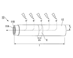
- FIG. 4 is a top view of FIG. 3. It is sectional drawing which shows other embodiment of the photoelectric conversion element which concerns on this invention. It is sectional drawing which shows other embodiment of the photoelectric conversion element which concerns on this invention. It is sectional drawing which shows an example of the conventional photoelectric conversion element. It is a perspective sectional view showing the modification of the electrode (first electrode) used with the photoelectric conversion element of the present invention.
- FIG. 1 It is a perspective sectional view showing other modifications of an electrode (first electrode) used in a photoelectric conversion element of the present invention.
- first electrode used in a photoelectric conversion element of the present invention.
- FIG. 1 It is the figure which showed the result of having measured the current-potential curve. It is the figure which showed typically the photoelectric conversion element of Example 2 and Example 3.
- FIG. 1 In the photoelectric conversion element of Example 1, it is the figure which showed the result of having measured the current-potential curve. It is the figure which showed typically the photoelectric conversion element of Example 2 and Example 3.
- FIG. 1 is a cross-sectional view illustrating an example of an electrode (first electrode) used in a photoelectric conversion element according to an embodiment of the present invention.
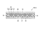
- FIG. 3 is a cross-sectional view illustrating an example of the photoelectric conversion element of the present embodiment
- FIG. 4 is a top view of FIG.
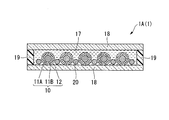
- a (1) of the present embodiment includes a linear first electrode 10; a linear second electrode 20; an electrolyte 17; and a pair of transparent substrates 18 and 18. And; a spacer 19 disposed on the peripheral edge of the pair of transparent substrates 18 and 18; Further, the first electrode 10 and the second electrode 10 are alternately arranged on one transparent substrate 18 with the electrolyte 17 interposed therebetween.
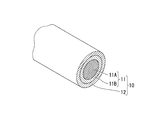
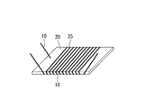
- the 1st electrode 10 used by this embodiment is the 1st wire 11 which consists of the copper wire 11A and the covering metal 11B (for example, titanium etc.) which coat
- a transparent conductive substrate in which a transparent conductive film such as FTO or ITO is formed on a transparent base made of glass, plastic, or the like is used as the first electrode (working electrode). Yes. Therefore, from the problem of heat resistance of the transparent base material, when glass is used as the transparent base material, these are baked at a temperature of about 150 ° C. or higher when plastic is used as the transparent base material, It was difficult to form a porous oxide semiconductor layer.
- the use of the metal wire for the first wire 11 eliminates the above-described problems and can be sufficiently fired even at a high temperature. Therefore, it is suitable as an electrode (working electrode) for a photoelectric conversion element.
- the first electrode 10 of the present embodiment has flexibility and can be used as an electrode for photoelectric conversion elements having various structures. Moreover, since the glass substrate and the transparent conductive film are not used unlike the conventional electrode, the first electrode 10 can be manufactured at low cost.
- the first wire 11 has a linear shape, and includes a copper wire 11A and a covering metal 11B that covers the copper wire 11A.
- a covering metal 11B in order to maintain the surface uniformity of the central metal (copper wire 11A) and improve the antioxidant rate, Ti or the like made of a material that is electrochemically inert to the electrolyte is used. Is preferred. In addition to Ti, Ni, W, Rh, and Mo can be used as the covering metal 11B. These alloys may be used.
- the copper wire 11A is preferably pure copper.
- the thinner the coating metal 11B the better.
- the thickness is too thin, there is a high probability that a pinhole or the like will occur in the coated metal 11B during the wire drawing process when the first wire 11 is manufactured.
- the copper wire 11A (copper) inside the covering metal 11B reacts with the electrolytic solution of the photoelectric conversion element, and the composition of the electrolytic solution changes. Thereby, the photoelectric conversion efficiency of a photoelectric conversion element will fall.
- the thickness of the covering metal 11B is increased, the frequency of occurrence of pinholes during the production of the first wire 11 decreases.
- more coating metal 11 is required, for example, when expensive Ti or the like is used, the cost is increased.
- the covering metal 11B has a lower conductivity than the copper wire 11A, if the covering metal 11B is thick, the conductivity of the photoelectric conversion element decreases, and as a result, the photoelectric conversion efficiency decreases. Therefore, it is preferable to make the thickness of the covering metal 11B thin as long as no pinhole is generated during wire drawing. Therefore, the following experiment was performed to determine the optimum thickness of the coated metal 11B.
- first wire rods 11 having wire diameters of ⁇ 0.05 mm, ⁇ 0.2 mm, and ⁇ 0.5 mm were produced.
- the thickness of the Ti layer of the first wire 11 having each wire diameter was set to 0.5 ⁇ m, 1.0 ⁇ m, 1.5 ⁇ m, 2.0 ⁇ m, and 3.0 ⁇ m, respectively.
- Each first wire 11 was wound around a bobbin and then poured into concentrated nitric acid and left for a whole day and night. Thereafter, the bobbin was taken out from the concentrated nitric acid, and the bobbin was washed and dried. Next, the film was wound by applying a constant tension (a load that is 1/2 of the breaking tension of the healthy part of the first wire 11).
- the pinhole frequency is greatly related to the thickness of the Ti layer (coating metal 11B). Moreover, when the thickness of the Ti layer was 2 ⁇ m or more, no pinhole was generated. When the thickness of the Ti layer was equal, the frequency of pinholes increased when the diameter of the first wire 11 was reduced. This is because the thickness distribution of the Ti layer occurred in the longitudinal direction of the first wire 11 during wire drawing, so the first wire 11 with a smaller diameter having a higher workability (easily caused by load), It is thought that the frequency of occurrence of pinholes in the longitudinal direction has increased.
- the thickness of the Ti layer (coating metal 11B) is preferably 2 ⁇ m or more as the condition of the first wire 11 applicable to the photoelectric conversion element.
- another metal Ni, W, Rh, Mo
- the voltage drop at this time be within 300 mV.
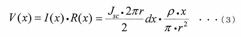
- the resistance value R (x) from one end of the first wire 11 to the point x is represented by the following formula (2). Note that ⁇ represents the conductivity of the first wire 11.
- the voltage drop amount of the entire first wire 11 is expressed by the following formula (4).
- the power generation current density, the length of the wire, the wire diameter, and the conductivity are adjusted so that the voltage drop amount V of the entire first wire 11 is 300 mV or less.
- the conductivity needs to be 67% or more.
- the covering metal 11B appropriately adjusts the area ratio between copper and the covering metal 11B so that the voltage drop is 300 mV or less according to the length and the wire diameter of the first wire 11.
- the coated metal 11B is Ti.
- Ti is formed into a pipe shape by extrusion molding or the like to produce a Ti pipe.
- copper is formed into a linear shape by extrusion molding or the like to produce a copper wire.
- a copper wire is inserted in the inside of a Ti pipe, these are squeezed, and both are stuck, and a Ti covering copper wire is obtained.
- the first wire 11 Ti-coated copper wire
- the Ti-coated copper wire is immersed in a TiO 2 paste, and then pulled up and dried.
- This process is repeated a total of three times to apply the TiO 2 paste to the surface of the Ti-coated copper wire. Thereafter, TiO 2 fine powder is further adhered to the surface of the Ti-coated copper wire, and sintered in an electric furnace at 500 ° C. for 1 hour. Thus, the porous TiO 2 film with Ti-coated copper wire is obtained. Next, a sensitizing dye is supported on the Ti-coated copper wire with a porous TiO 2 film. Thus, the first electrode 10 is produced.
- Ti was used as the covering metal 11B has been described, the same applies to the case where Ni, W, Rh, and Mo are used.
- the porous oxide semiconductor layer 12 is provided around the first wire 11 and a sensitizing dye is supported on at least a part of the surface thereof.
- the porous oxide semiconductor layer 12 may cover only a part of the outer periphery of the first wire 11.
- the porous oxide semiconductor layer 12 has a decrease in light collection ability, promotion of reverse electron transfer reaction, and the like. It is preferable to completely cover the outer periphery.
- the semiconductor for forming the porous oxide semiconductor layer 12 is not particularly limited, and any semiconductor can be used as long as it is generally used for forming a porous oxide semiconductor for a photoelectric conversion element.
- a semiconductor for example, titanium oxide (TiO 2 ), tin oxide (SnO 2 ), zinc oxide (ZnO), niobium oxide (Nb 2 O 5 ), tungsten oxide (WO 3 ), or the like can be used. .
- Examples of the method for forming the porous oxide semiconductor layer 12 include the following methods. First, a desired additive is added to a dispersion obtained by dispersing commercially available oxide semiconductor fine particles in a desired dispersion medium or a colloid solution prepared by a sol-gel method, if necessary. Then, after this solution is disposed on the outer periphery of the first wire 11 by a method such as dipping, coating, and extrusion, the porous oxide semiconductor layer 12 is formed on the outer periphery of the first wire 11 by firing.
- the thickness of the porous oxide semiconductor layer 12 is not particularly limited, but is preferably 1 ⁇ m to 50 ⁇ m, for example.
- ruthenium complexes such as N3 and black dye, metal-containing complexes such as porphyrin and phthalocyanine, and organic dyes such as eosin, rhodamine and merocyanine can be applied. What has taken the excitation behavior suitable for a semiconductor should just be selected suitably.
- the second electrode 20 has a linear shape and is made of, for example, platinum (Pt), Pt-coated Ti wire and Ti composite wire, carbon, carbon-coated Ti wire and Ti composite wire, or a conductive polymer. Also, a linear substrate made of a material that is electrically conductive and electrochemically inactive with respect to the electrolyte is coated with Pt, or the linear substrate is coated with carbon or a conductive polymer. This is also used as the second electrode 20. In such a second electrode 20, transfer of charges with the electrolyte proceeds promptly.
- the linear base material include inert metals such as Ti, Ni, W, Rh, and Mo, or carbon fibers. A plate-like one may be used as the second electrode 20.
- the first electrode 10 having a porous oxide semiconductor layer carrying a sensitizing dye is wound around the outer periphery of the plate-like second electrode 20 via a separator such as a net-like nylon fiber.
- a photoelectric conversion element is manufactured (see FIG. 10).
- the carbon examples include graphitized (crystallized) carbon, amorphous carbon, fullerene, carbon nanotube, and carbon fiber.
- particles such as carbon black may be pasted and applied to a linear substrate, Ti wire, or the like.
- the conductive polymer constituting the material of the second electrode 20 include a PEDOT [Poly (3,4-ethylenedioxythiophene): “polyethylenedioxythiophene]] derivative and a PANI [Polyaniline] derivative. .
- the diameter of the second electrode 20 is preferably 1 ⁇ 4 or less of the diameter of the first electrode 10. .
- the several 1st electrode 10 can be arrange
- the diameter of the second electrode 20 is preferably about 1 ⁇ 4 of the diameter of the first electrode 10.
- it is preferable that the 1st wire 11 is pulled out of the element. Thereby, the generated electricity can be easily taken out.
- the electrolyte 17 is obtained by impregnating the porous oxide semiconductor layer 12 with an electrolytic solution; after impregnating the porous oxide semiconductor layer 12 with the electrolytic solution, the electrolytic solution is used with an appropriate gelling agent. Formed into an integral body with the porous oxide semiconductor layer 12; based on an ionic liquid; or a gel electrolyte containing oxide semiconductor particles and conductive particles Etc. are used.
- electrolyte solution what melt
- dissolved electrolyte components such as an iodine, iodide ion, and tertiary butyl pyridine, in organic solvents and ionic liquids, such as ethylene carbonate and methoxyacetonitrile, is used.
- the gelling agent used for gelling the electrolytic solution include polyvinylidene fluoride, a polyethylene oxide derivative, and an amino acid derivative.
- the ionic liquid is a liquid at room temperature
- the normal temperature molten salt which used the compound which has the quaternized nitrogen atom as a cation is mentioned.
- the cation of the room temperature molten salt include quaternized imidazolium derivatives, quaternized pyridinium derivatives, and quaternized ammonium derivatives.
- the anion of the room temperature molten salt include BF 4 ⁇ , PF 6 ⁇ , (HF) n ⁇ , bistrifluoromethylsulfonylimide [N (CF 3 S0 2 ) 2 ⁇ ], iodide ions, and the like.
- Specific examples of the ionic liquid include salts composed of quaternized imidazolium-based cations, iodide ions or bistrifluoromethylsulfonylimide ions.
- the oxide semiconductor particles are not particularly limited in terms of the type and particle size of the substance, but those having excellent miscibility with an electrolytic solution mainly composed of an ionic liquid and gelling the electrolytic solution are used. Further, the oxide semiconductor particles are required to have excellent chemical stability against other coexisting components contained in the electrolyte without reducing the semiconductivity of the electrolyte. In particular, even when the electrolyte contains a redox pair such as iodine / iodide ions or bromine / bromide ions, the oxide semiconductor particles are preferably those that do not deteriorate due to an oxidation reaction.
- oxide semiconductor particles examples include TiO 2 , SnO 2 , SiO 2 , ZnO, Nb 2 O 5 , In 2 O 3 , ZrO 2 , Al 2 O 3 , WO 3 , SrTiO 3 , Ta 2 O 5 , One or a mixture of two or more selected from the group consisting of La 2 O 3 , Y 2 O 3 , Ho 2 O 3 , Bi 2 O 3 and CeO 2 is preferred.
- the average particle size of the oxide semiconductor particles is preferably about 2 nm to 1000 nm.
- conductive particles such as a conductor and a semiconductor are used.
- the type and particle size of the conductive particles are not particularly limited, and those that are excellent in miscibility with an electrolytic solution mainly composed of an ionic liquid and that gel the electrolytic solution are used. Furthermore, it is necessary to be excellent in chemical stability against other coexisting components contained in the electrolyte. In particular, even when the electrolyte contains an oxidation / reduction pair such as iodine / iodide ion or bromine / bromide ion, an electrolyte that does not deteriorate due to oxidation reaction is preferable.
- Examples of such conductive fine particles include those composed of a substance mainly composed of carbon, and specific examples include particles such as carbon nanotubes, carbon fibers, and carbon black. All methods for producing these substances are known, and commercially available products can also be used.
- the transparent base material 18 a substrate made of a light-transmitting material is used, and a non-alkali glass substrate, other glass substrate, resin substrate such as glass, polyethylene terephthalate, polycarbonate, polyethersulfone, etc., usually photoelectric conversion. Any material can be used as long as it is used as a transparent substrate of the element.
- the transparent substrate 18 is appropriately selected from these in consideration of resistance to the electrolytic solution.
- substrate which is as excellent in light transmittance as possible is preferable on a use, and the board
- the spacer 19 is not particularly limited as long as it has excellent adhesion to the transparent substrate 18, but for example, an adhesive made of a thermoplastic resin having a carboxylic acid group in the molecular chain is desirable.
- an adhesive made of a thermoplastic resin having a carboxylic acid group in the molecular chain is desirable.
- UV curable materials e.g., 31X-101 (Three Bond Co., Ltd.)] and the like can be mentioned.
- the photoelectric conversion element 1 of the present embodiment has a completely different structure from the conventional photoelectric conversion element 1 that does not require a conductive substrate.
- a metal substrate (first wire 11) having good corrosion resistance is used, and a transparent substrate 18 that is transparent but not conductive is used to seal the electrolyte 17. Therefore, unlike a conventional electrode, a glass substrate or a transparent conductive film is not used, so that an electrode (first electrode or second electrode) can be manufactured at low cost.
- the second electrode 20 is also linear, and the second electrode 20 is arranged in the gap between the first electrodes 10, thereby providing a space in the photoelectric conversion element 1.
- the photoelectric conversion element 1 of this embodiment since the distance between the light-incident side glass plate (transparent substrate) and the surface of the power generation unit (porous oxide semiconductor layer) can be shortened, an improvement in power generation amount is expected. it can.
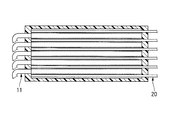
- FIG. 5 is a cross-sectional view showing the photoelectric conversion element 1B (1) according to this embodiment.
- the differences from the first embodiment described above will be mainly described, and the description of the same parts will be omitted.
- the second electrode 20 is disposed above and below the first electrode 10 (arranged on the pair of transparent base materials 18 and 18). Is substantially the same as in the first embodiment.
- the photoelectric conversion efficiency can be improved. For light incidence from the vertical direction, even if the number of second electrodes 20 functioning as counter electrodes is increased, the photoelectric conversion efficiency hardly decreases.
- FIG. 6 is a cross-sectional view showing the photoelectric conversion element 1C (1) according to this embodiment.
- the differences from the first embodiment described above will be mainly described, and the description of the same parts will be omitted.
- the second electrodes 20 having substantially the same diameter as the first electrode 10 are alternately arranged on the left and right of the first electrode 10. This is almost the same as the embodiment.
- the resulting photoelectric conversion element 1C becomes linear, and this photoelectric conversion
- the element 1C can be easily arranged at various parts.
- the shapes of the first electrode 10 and the second electrode may be irregular lines such as a flat wire, a triangle or more polygonal line.
- a Ti-coated copper wire (first wire) having a diameter of 1.0 mm was produced by the method described above.
- this Ti-coated copper wire was dipped in a TiO 2 paste (manufactured by Solaronix, Ti Nanoxide-T), then pulled up and dried. This process was performed three times in total, and after applying a TiO 2 paste to the surface of the Ti-coated copper wire, sintering was performed at 500 ° C. for 1 hour in an electric furnace to produce a Ti wire with a TiO 2 film.
- the application range of TiO 2 was 5 cm long, and the thickness of the TiO 2 film was approximately 6 ⁇ m.
- a ruthenium dye (manufactured by Solaronix, Ruthenium535-BisTBA, generally called N719) is dissolved in a mixed solution of acetonitrile and tert-butanol in a 1: 1 ratio to prepare a 0.3 mM ruthenium dye solution. did. Then, the Ti wire with the TiO 2 film was immersed in this ruthenium dye solution and allowed to stand at room temperature for 24 hours to support the ruthenium dye on the TiO 2 surface. Next, after pulling up the Ti wire with the TiO 2 film from the ruthenium dye solution, it was washed with the above mixed solution, and this was used as a working electrode (first electrode). Five working electrodes were produced in the same process.
- Example 2 8 m of Ti-coated copper wire (first wire) drawn to a diameter of 0.2 mm was prepared. At this time, the area ratio of copper to titanium was 40% (the area ratio of titanium was 60%). Next, this Ti-coated copper wire was immersed in a TiO 2 paste (manufactured by Solaronix, Ti Nanoxide-T), then pulled up and dried. This process was performed three times in total to apply a TiO 2 paste on the surface of the Ti-coated copper wire, and then sintered in an electric furnace at 500 ° C. for 1 hour to obtain a Ti wire with a porous TiO 2 film. The film thickness of TiO 2 was approximately 6 ⁇ m.
- ruthenium dye (Solaronix, Ruthenium535-BisTBA) was dissolved in a mixed solution of acetonitrile and tert-butanol mixed at 1: 1 to prepare a 0.3 mM ruthenium dye solution. Then, the Ti wire with the TiO 2 film was immersed in this ruthenium dye solution and allowed to stand at room temperature for 24 hours to support the ruthenium dye on the TiO 2 surface. Next, after pulling up the Ti wire with the TiO 2 film from the ruthenium dye solution, it was washed with the above mixed solution, and this was used as a working electrode (first electrode).
- a 10 cm ⁇ 10 cm Ti plate (thickness 1 mm) in which platinum was sputtered to a thickness of 200 nm was prepared. And as shown in FIG. 10, the 1st electrode was wound around the 2nd electrode. At this time, when the first electrode and the second electrode are in direct contact with each other, a short circuit occurs and the photoelectric conversion element does not function. Therefore, a net-like nylon fiber having a thickness of 16 ⁇ m is arranged around the second electrode, and the first electrode is wound around the second electrode through the nylon fiber.
- the first electrode and the second electrode were immersed in a volatile electrolyte (electrolytic solution) using methoxyacetonitrile as a solvent to obtain a photoelectric conversion element of Example 2.
- a box shape may be formed by combining polyethylene naphthalate or glass.
- the length of the first electrode in which the voltage drop occurs may be half of the total length. That is, for the calculation of the voltage drop amount V, 4 m which is half of the total length of 8 m was used. In calculating the voltage drop, 10 mA / cm 2 was used as the generated current density.
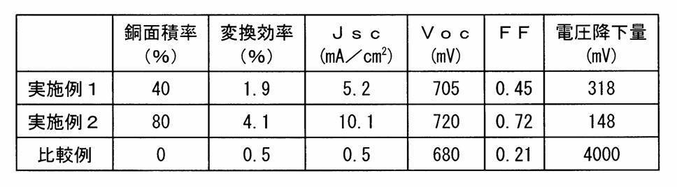
- Example 2 The photoelectric conversion element of Example 2 produced as described above was irradiated with light using a solar simulator (AM1.5, 100 mW / cm 2 ), and a current-potential curve was measured. The results are shown in Table 2. Table 2 also shows the amount of voltage drop of this example obtained by the above equation (4).
- Example 3 Regarding the Ti-coated copper wire (first wire) of Example 2, it was produced in the same manner as in Example 2 except that the area ratio of copper to titanium was 80% (the area ratio of titanium was 20%). Was used as the photoelectric conversion element of Example 3. The photoelectric conversion element of Example 3 was irradiated with light using a solar simulator in the same manner as in Example 2, and a current-potential curve was measured. The results are shown in Table 2. Table 2 also shows the amount of voltage drop of this example obtained by the above equation (4).
- photoelectric conversion efficiency is improved by using a first wire (Ti-coated copper wire) in which a copper wire is coated with a coated metal (titanium) instead of a pure titanium wire. It was confirmed to improve. Further, from the results of Examples 2 and 3, the photoelectric conversion efficiency is further improved by lowering the area ratio of the coated metal (titanium) (increasing the area ratio of the copper wire) and setting the voltage drop amount to 300 mV or less. It was confirmed that a high-performance photoelectric conversion element was obtained.
- Photoelectric conversion element 10 First electrode 11 First wire 11A Copper wire 11B Coated metal 12 Porous oxide semiconductor layer 20 Second electrode 17 Electrolyte 18 Transparent substrate 19 Sealing material
Landscapes
- Engineering & Computer Science (AREA)
- Power Engineering (AREA)
- Microelectronics & Electronic Packaging (AREA)
- Chemical & Material Sciences (AREA)
- Chemical Kinetics & Catalysis (AREA)
- Electrochemistry (AREA)
- Hybrid Cells (AREA)
- Photovoltaic Devices (AREA)
- Materials Engineering (AREA)
- Cell Electrode Carriers And Collectors (AREA)
Abstract
Description
本願は、2008年6月6日に、日本に出願された特願2008-149922号に基づき優先権を主張し、その内容をここに援用する。
この色素増感型太陽電池100は、増感色素が担持された多孔質半導体電極(以下、色素増感半導体電極とも呼ぶ)103が一方の面に形成された第一基板101と;導電膜104が形成された第二基板105と;これらの間に封入された例えばヨウ素/ヨウ化物イオンなどの酸化還元対を含む電解質106と;を主な構成要素としている。
一方、第二基板105の電解質106と接する側の面には、導電性を持たせるために、例えば炭素や白金からなる導電層104が設けられている。これら第二基板105及び導電層104により対極109が構成されている。
上記(1)に記載の光電変換素子によれば、導電性基板が不要となり、低コスト化が図れる。また、中心金属に銅線を用い、その外周に被覆金属が配置された構造とすることにより、中心金属を単一の金属線材とするよりも、耐食性に優れ、導電線の導電率を高めかつ低コスト化を図ることができる。また、線状をなす第一電極の外周面が受光面となるため、照射光に対する投影面積を増大でき、かつ光入射角度依存性が少なくなる。
上記(3)の場合、光電変換素子の発電効率の向上が図れる。
上記(4)の場合、銅線の表面の均一性が維持され、かつ銅線の酸化を防止した状態で、光電変換素子の発電効率の向上が図れる。
上記(5)の場合、被覆金属にピンホールが発生するのを抑制でき、銅線と光電変換素子の電解液とが反応して、電解液の組成が変化するのを抑制できる。この結果、光電変換素子の光電変換効率が低下するのを防止できる。
上記(6)の場合、得られる光電変換素子が線状となり、この光電変換素子を多様な部位に容易に配置することができる。
特に、第一線材の構成として、中心金属に銅線を用い、その外周が例えばチタン等で被覆された構造とすることにより、中心金属を、例えばチタン(Ti)、ニッケル(Ni)、タングステン(W)、ロジウム(Rh)、モリブデン(Mo)等から選択された単一の金属線材とするよりも、耐食性に優れ、第一線材の導電率を高めかつ低コスト化が図れる。
以下、本発明の実施の形態を、図面を参照して説明する。
本実施形態の光電変換素子1A(1)は、図3に示すように、線状の第一電極10と;線状の第二電極20と;電解質17と;一対の透明基材18,18と;これら一対の透明基材18,18の周縁部に配置されたスペーサー19と;を有する。また、第一電極10と第二電極10とが電解質17を介して交互に、一方の透明基材18上に配置されている。これら第一電極10と第二電極20と電解質17とが、一対の透明基材18,18とスペーサー19とにより封止されている。
図1及び図3に示すように、本実施形態で用いている第一電極10は、銅線11Aとこの銅線11Aを被覆する被覆金属11B(例えばチタン等)とからなる第一線材11と;この第一線材11の外周に配され、増感色素が担持された多孔質酸化物半導体層12と;から構成されている。
これに対して、本実施形態の第一電極10では、第一線材11に金属線を採用したことにより、上記のような問題がなく、高温でも十分に焼成できる。そのため、光電変換素子用の電極(作用極)として好適である。
さらに、従来の電極のようにガラス基板や、透明導電膜を用いないため、安価にこの第一電極10を製造することができる。
被覆金属11Bとしては、中心金属(銅線11A)の表面の均一性の維持や、酸化防止率を向上させるために、電解質に対して電気化学的に不活性な材質からなるTi等を用いるのが好ましい。また、被覆金属11Bとして、Tiの他、Ni、W、Rh、Moを用いることが出来る。なお、これらの合金を用いても良い。
銅線11Aは、純銅が好ましい。
一方、被覆金属11Bの厚さを厚くすると、第一線材11の作製時にピンホールが発生する頻度は低下する。しかしながら、より多くの被覆金属11を必要とするため、例えば高価なTi等を用いた場合では、コストアップにつながる。また、被覆金属11Bは、銅線11Aよりも導電率が低いため、この被覆金属11Bが厚いと光電変換素子の導電率が低下し、結果として光電変換効率が低下してしまう。
したがって、被覆金属11Bの厚さは、伸線時にピンホールが発生しない範囲で、薄くするのが好ましい。そこで、最適な被覆金属11Bの厚さを決定するため、以下の実験を行なった。
各第一線材11をボビンに巻いた後、濃硝酸中に投入し、一昼夜放置した。その後、濃硝酸中からボビンを取り出して、ボビンの洗浄、乾燥を行った。次いで、一定の張力(第一線材11の健全部の破断張力の1/2となる荷重)を加えて巻き返しを行なった。Ti層にピンホールが存在する箇所では、硝酸によって内部の銅(銅線11A)が溶けているため、破断張力が低下し、断線する。よって、巻き返しを行った際の断線頻度を記録することで、どの程度のピンホールが被覆金属11Bに存在しているかを調査できる。結果を、表1に示す。
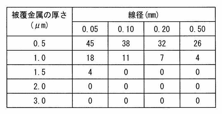
よって、光電変換素子に適用できる第一線材11の条件として、Ti層(被覆金属11B)の厚さは、2μm以上が好ましいと考えられる。なお、被覆金属11Bとして他の金属(Ni、W、Rh、Mo)を用いた場合も同様である。
チタン等の被覆金属11Bで銅線11Aが被覆された第一線材11の場合、第一線材11に焼結されたTiO2等の多孔質酸化物半導体層12により発生された電流が、第一線材11の内部を通り、集電部に到着する。よって、第一線材11の抵抗が低いほど電圧降下が抑制され、太陽電池の性能は高くなる。一般に、このときの電圧降下は300mV以内であることが実用上望ましい。
(1)第一線材11の線径については、線径が小さくなると抵抗が高くなる。また、この線径が小さいと、第一電極10での受光面積が低下し、発電電流の絶対量が低くなる。
(2)第一線材11の長さは、短いと抵抗が低くなる。ゆえに、短い方が好ましい。
(3)チタン等の被覆金属11Bは、銅に比べると抵抗が高いため、被覆金属11Bの面積は少なくする必要がある。
すなわち、第一線材11の線径や長さ、導電率、発電電流密度により、電圧降下量は変動することになる。例えば、図2に示すように、第一電極10の上半部にのみ光が入射し、発電が行なわれる場合について考える。図2において、rが第一線材11の半径、lが第一線材11の長さ、dxが、第一線材11のx地点での幅を示している。この場合、幅dxで発生する電流量I(x)は、以下の式(1)で表される。
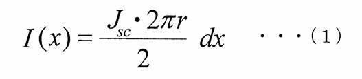


例えば、第一線材11の線径が200μm、長さが4m、発電電流密度が10mA/cm2の場合、導電率は67%以上にする必要がある。この値を達成するためには、第一線材11の銅の面積比率が、被覆金属11Bに対して65%以上となるように、被覆金属11Bを銅線11Aに形成する必要がある。
このように、被覆金属11Bは、第一線材11の長さや線径に応じ、電圧降下が300mV以下となるように、銅と被覆金属11Bとの面積比率を適宜調整するのが好ましい。
次に、この第一線材11を第一電極10とするには、Ti被覆銅線をTiO2ペースト中に侵漬した後、引き上げ、乾燥を行なう。この工程を合計3回繰り返して、TiO2ペーストをTi被覆銅線の表面に塗布する。その後、さらにTi被覆銅線の表面にTiO2微粉末を付着させ、電気炉にて500℃で1時間焼結する。これにより、多孔質TiO2膜付きTi被覆銅線が得られる。次に、この多孔質TiO2膜付きTi被覆銅線に増感色素を担持させる。以上で、第一電極10が作製される。なお、被覆金属11BとしてTiを用いた場合を説明したが、Ni、W、Rh、Moを用いた場合も同様である。
多孔質酸化物半導体層12は、第一線材11の外周の一部のみを覆うものであってもよいが、光収集能力の低下、逆電子移動反応の促進等があるため、第一線材11の外周を完全に覆うことが好ましい。
このような多孔質酸化物半導体層12の厚みとしては、特に限定されるものではないが、例えば、1μm~50μmが好ましい。
また、導電性を有し、かつ、電解質に対して電気化学的に不活性な材質からなる線状基材をPtで被覆したものや、前記線状基材をカーボンや導電性高分子で被覆したものも第二電極20として用いられる。このような第二電極20では、電解質との電荷の授受が速やかに進行する。
この線状基材としては、具体的には、例えば、Ti、Ni、W、Rh、Moなどの不活性金属、あるいは炭素繊維などが挙げられる。
第二電極20として、板状のものを用いてもよい。この場合、板状の第二電極20の外周に、例えば網状のナイロン繊維等のセパレータを介して、増感色素が担持された多孔質酸化物半導体層を有する第一電極10を巻きつけることで、光電変換素子が作製される(図10参照)。
また、第二電極20の材料を構成する導電性高分子としては、例えば、PEDOT[Poly(3,4-ethylenedioxythiophene):「ポリエチレンジオキシチオフェン」]誘導体や、PANI[Polyaniline]誘導体などが挙げられる。
しかし、第二電極20が細くなると抵抗が増加するため、より太い方が好ましい。よって、第二電極20の直径は、第一電極10の直径の1/4程度とすることが好ましい。
また、図4に示すように、第一線材11は、素子の外部へと引き出されていることが好ましい。これにより、発電した電気を容易に外部へと取り出すことが可能である。
この電解液をゲル化する際に用いられるゲル化剤としては、ポリフッ化ビニリデン、ポリエチレンオキサイド誘導体、アミノ酸誘導体などが挙げられる。
また、揮発性電解質溶液に代えて、一般に色素増感型太陽電池に用いられるものであれば、溶媒がイオン液体であるものやゲル化したものだけではなく、p型無機半導体や有機ホール輸送層といった固体であっても制限なく使用可能である。
常温溶融塩のカチオンとしては、四級化イミダゾリウム誘導体、四級化ピリジニウム誘導体、四級化アンモニウム誘導体などが挙げられる。
常温溶融塩のアニオンとしては、BF4 -、PF6 -、(HF)n -、ビストリフルオロメチルスルホニルイミド[N(CF3S02)2 -]、ヨウ化物イオンなどが挙げられる。
イオン液体の具体例としては、四級化イミダゾリウム系カチオンや、ヨウ化物イオンまたはビストリフルオロメチルスルホニルイミドイオンなどからなる塩類を挙げることができる。
導電性粒子の種類や粒子サイズなどは特に限定されないが、イオン液体を主体とする電解液との混和性に優れ、この電解液をゲル化するようなものが用いられる。さらに、電解質に含まれる他の共存成分に対する化学的安定性に優れることが必要である。特に、電解質がヨウ素/ヨウ化物イオンや、臭素/臭化物イオンなどの酸化還元対を含む場合でも、酸化反応による劣化を生じないものが好ましい。
導電性は耐食性の良い例えば金属線(第一線材11)に担わせ、電解質17を封止するために、透明だが導電性を持たない透明基材18を用いた。そのため、従来の電極のようにガラス基板や、透明導電膜を用いないため、安価に電極(第一電極や第二電極)を製造できる。また、第一線材11の中心線として、高耐食性、高導電率、かつ低コストな銅線を用い、この中心線がTi等で被覆された金属複合線(第一線材)を用いることにより、この金属複合線の耐食性を高めておきながら導電率を高く保持することができ、かつそのコストを低く抑えることもできる。
また、線状をなす第一電極10の外周面が受光面となる(例えば図4参照)ため、照射光に対する投影面積を増大することができ、かつ光入射角度依存性が少なくなる。
また、本実施形態の光電変換素子1によれば、第二電極20も線状にし、第一電極10間の間隙部にこの第二電極20を配することにより、光電変換素子1内のスペースをより有効に利用できる。この結果、さらに薄型の光電変換素子が得られる。
また、本実施形態の光電変換素子1によれば、入光側のガラス板(透明基板)と発電部(多孔質酸化物半導体層)表面との距離を短くできることから、発電量の向上が期待できる。
以下、本発明の第二実施形態に係る光電変換素子1を、図5に基づいて説明する。
図5は、本実施形態に係る光電変換素子1B(1)を示す断面図である。本実施形態では、上述した第一実施形態との相違点を中心に述べ、同様の部分についてはその説明を省略する。
本実施形態のように第二電極20を第一電極10の上下に配することで、第一電極10と第二電極20との間で距離の離れている部分を少なくできる。ゆえに、光電変換効率の向上が図れる。鉛直方向からの光入射に対しては、対極として機能する第二電極20の数を増やしても、光電変換効率の低下は殆ど生じない。
本発明の第三実施形態に係る光電変換素子1を、図6に基づいて説明する。
図6は、本実施形態に係る光電変換素子1C(1)を示す断面図である。本実施形態では、上述した第一実施形態との相違点を中心に述べ、同様の部分についてはその説明を省略する。
本実施形態のように第一電極10とほぼ同様の径を有する第二電極20を、第一電極10の左右交互に配することで、得られる光電変換素子1Cが線状となり、この光電変換素子1Cを多様な部位に容易に配置できる。
まず、直径1.0mmのTi被覆銅線(第一線材)を、上述した方法で作製した。次に、このTi被覆銅線をTiO2ペースト(Solaronix社製、Ti Nanoxide-T)に浸漬し、その後引き上げ、乾燥を行なった。この工程を合計3回行なって、Ti被覆銅線の表面にTiO2ペーストを塗布した後、電気炉で500℃、1時間焼結して、TiO2膜付きTiワイヤを作製した。TiO2の塗布範囲は長さ5cmとし、TiO2膜の厚さはおよそ6μmであった。
次に、アセトニトリルとtert-ブタノールとが1:1で混合した混合溶液にルテニウム色素(Solaronix社製、Ruthenium535-BisTBA、一般にはN719と呼ばれる)を溶解して、0.3mMのルテニウム色素溶液を作製した。そして、このルテニウム色素溶液に上記TiO2膜付きTiワイヤを浸漬し、室温にて24時間放置して、TiO2表面にルテニウム色素を担持させた。次いで、このルテニウム色素溶液からTiO2膜付きTiワイヤを引き上げた後、上記混合溶液で洗浄し、これを作用極(第一電極)とした。この作用極を、同様な工程で5本作製した。
対極として直径0.08mmのPtワイヤ6本を用意し、これら6本の対極と、5本の上記作用極とを交互に無アルカリガラス基板上に並べた。次いで、厚さ1.0mmのPETフィルムをスペーサーとして上記無アルカリガラス基板の周縁部に配置し、これらを、メトキシアセトニトリルを溶媒とする揮発性電解質に浸した。次いで、スペーサーを介して無アルカリガラスを上面に被せて、図3に示す実施例1の光電変換素子を作製した。
本実施例については、金属ワイヤ(作用極及び対極)を特に制御することなく並べたものであるので、セルの受光面積は、ワイヤ間の隙間が占める面積も含めて、およそ5cm×0.15cm=0.75cm2程度である。作用極の受光面積(アクティブエリア)は、色素担持TiO2膜付きTiワイヤの投影面積なので、5cm×0.0212cm×5本=0.53cm2とすることが可能であり、短絡電流密度の見積もりに1.5倍程度の誤差を含む。
図9より、Jsc=2.4mA/cm2、VOC=730mV、ff=0.71であり、光電変換効率は、1.25%を示した。
直径0.2mmまで伸線したTi被覆銅線(第一線材)を、8m用意した。この際、チタンに対する銅の面積率を40%(チタンの面積率は60%)とした。次に、このTi被覆銅線を、TiO2ペースト(Solaronix社製、Ti Nanoxide-T)に浸漬し、その後引き上げ、乾燥を行なった。この工程を合計3回行なってTi被覆銅線の表面にTiO2ペーストを塗布した後、500℃の電気炉にて、1時間焼結して、多孔質TiO2膜付きTiワイヤを得た。TiO2の膜厚は、およそ6μmであった。
次に、アセトニトリルとtert-ブタノールとが1:1で混合した混合溶液にルテニウム色素(Solaronix社製、Ruthenium535-BisTBA)を溶解して、0.3mMのルテニウム色素溶液を作製した。そして、このルテニウム色素溶液に上記TiO2膜付きTiワイヤを浸漬し、室温にて24時間放置して、TiO2表面にルテニウム色素を担持させた。次いで、このルテニウム色素溶液からTiO2膜付きTiワイヤを引き上げた後、上記混合溶液で洗浄し、これを作用極(第一電極)とした。
対極(第二電極)として、プラチナが200nmの厚さでスパッタされた10cm×10cmのTi板(厚さ1mm)を用意した。そして、図10に示すように、第一電極を第二電極に巻きつけた。この際、第一電極と第二電極とが直接接触すると短絡し、光電変換素子として機能しなくなる。そこで、第二電極の周囲には、厚さ16μmの網状のナイロン繊維を配置し、このナイロン繊維を介して、第一電極を第二電極に巻きつけた。
次に、この第一電極と第二電極とをメトキシアセトニトリルを溶媒とする揮発性電解質(電解液)に浸し、実施例2の光電変換素子とした。なお、電解液を保持するケースとしては、透光性を有し、電解液に耐えられる材料であれば特に限定されない。例えば、ポリエチレンナフタレートやガラスを組み合わせて箱状に形成すればよい。
なお、本実施例では、巻きつけた第一電極の両端から集電を行なっているので、電圧降下が起きる第一電極の長さは、全長の半分を考慮すればよい。つまり、電圧降下量Vの計算には、全長8mの半分の4mを用いた。電圧降下量の計算には、発電電流密度として、10mA/cm2を用いた。
実施例2のTi被覆銅線(第一線材)に関し、チタンに対する銅の面積率を80%(チタンの面積率は20%)としたこと以外は、実施例2と同様にして作製し、これを実施例3の光電変換素子とした。
実施例3の光電変換素子に、実施例2と同様にソーラーシミュレータを用いて光を照射し、電流電位曲線を測定した。その結果を、表2に示す。また表2には、上記式(4)で求めた本実施例の電圧降下量も示す。
実施例2のTi被覆銅線(第一線材)に変わり、純チタン線を用いたこと以外は実施例2と同様に作製し、これを比較例1の光電変換素子とした。そして、比較例1の光電変換素子に、実施例2と同様にソーラーシミュレータを用いて光を照射し、電流電位曲線を測定した。その結果を、表2に示す。また表2には、上記式(4)で求めた比較例の電圧降下量も示す。
10 第一電極
11 第一線材
11A 銅線
11B 被覆金属
12 多孔質酸化物半導体層
20 第二電極
17 電解質
18 透明基材
19 封止材
Claims (6)
- 線状をなす第一電極と、第二電極と、電解質と、を有する光電変換素子であって、
前記第一電極と前記第二電極とが前記電解質を介して配置され、
前記第一電極は、銅線及びこの銅線を被覆する被覆金属からなる第一線材と、この第一線材の外周に配され、色素が担持された多孔質酸化物半導体層と、からなる
ことを特徴とする光電変換素子。 - 前記被覆金属が、チタン、ニッケル、タングステン、ロジウム、モリブデンから選ばれたいずれか一の金属からなる
ことを特徴とする請求項1に記載の光電変換素子。 - 前記第一線材の電圧降下量が300mV以下である
ことを特徴とする請求項1または2に記載の光電変換素子。 - 前記銅線の前記被覆金属に対する面積比率が、前記電圧降下量が300mV以下となるような面積比率で、前記銅線が前記被覆金属に被覆されている
ことを特徴とする請求項3に記載の光電変換素子。 - 前記被覆金属の膜厚が2μm以上である
ことを特徴とする請求項1から4のいずれかに記載の光電変換素子。 - 前記第二電極が線状をなし、前記第一電極と前記第二電極とが交互に配置されている
ことを特徴とする請求項1から4のいずれかに記載の光電変換素子。
Priority Applications (5)
| Application Number | Priority Date | Filing Date | Title |
|---|---|---|---|
| JP2009548508A JP5114499B2 (ja) | 2008-06-06 | 2009-06-08 | 光電変換素子 |
| EP09758448.6A EP2284942A4 (en) | 2008-06-06 | 2009-06-08 | Photoelectric conversion element |
| CN2009801199556A CN102047497A (zh) | 2008-06-06 | 2009-06-08 | 光电转换元件 |
| AU2009255031A AU2009255031A1 (en) | 2008-06-06 | 2009-06-08 | Photoelectric conversion element |
| US12/960,228 US8841543B2 (en) | 2008-06-06 | 2010-12-03 | Photoelectric conversion element |
Applications Claiming Priority (2)
| Application Number | Priority Date | Filing Date | Title |
|---|---|---|---|
| JP2008-149922 | 2008-06-06 | ||
| JP2008149922 | 2008-06-06 |
Related Child Applications (1)
| Application Number | Title | Priority Date | Filing Date |
|---|---|---|---|
| US12/960,228 Continuation US8841543B2 (en) | 2008-06-06 | 2010-12-03 | Photoelectric conversion element |
Publications (1)
| Publication Number | Publication Date |
|---|---|
| WO2009148181A1 true WO2009148181A1 (ja) | 2009-12-10 |
Family
ID=41398252
Family Applications (1)
| Application Number | Title | Priority Date | Filing Date |
|---|---|---|---|
| PCT/JP2009/060468 WO2009148181A1 (ja) | 2008-06-06 | 2009-06-08 | 光電変換素子 |
Country Status (7)
| Country | Link |
|---|---|
| US (1) | US8841543B2 (ja) |
| EP (1) | EP2284942A4 (ja) |
| JP (1) | JP5114499B2 (ja) |
| KR (1) | KR20100133486A (ja) |
| CN (1) | CN102047497A (ja) |
| AU (1) | AU2009255031A1 (ja) |
| WO (1) | WO2009148181A1 (ja) |
Cited By (1)
| Publication number | Priority date | Publication date | Assignee | Title |
|---|---|---|---|---|
| JP2010123515A (ja) * | 2008-11-21 | 2010-06-03 | Fujikura Ltd | 光電変換素子 |
Families Citing this family (4)
| Publication number | Priority date | Publication date | Assignee | Title |
|---|---|---|---|---|
| KR20110053957A (ko) * | 2008-08-29 | 2011-05-24 | 신닛테츠가가쿠 가부시키가이샤 | 색소 증감 태양 전지 및 그 제조 방법 |
| JP5398440B2 (ja) * | 2009-09-11 | 2014-01-29 | 株式会社フジクラ | 光電変換素子 |
| KR101816275B1 (ko) | 2010-12-23 | 2018-01-09 | 삼성디스플레이 주식회사 | 백라이트 어셈블리를 갖는 표시 장치 |
| WO2013091725A1 (en) * | 2011-12-23 | 2013-06-27 | Aurubis Ag | A conductor spool, a method for manufacturing a solar cell and a solar cell |
Citations (8)
| Publication number | Priority date | Publication date | Assignee | Title |
|---|---|---|---|---|
| JPH01220380A (ja) | 1988-02-12 | 1989-09-04 | Gebr Sulzer Ag | 光電気化学電池・その製法及び使用法 |
| JP2000021460A (ja) * | 1998-07-03 | 2000-01-21 | Toyota Central Res & Dev Lab Inc | 色素増感型太陽電池 |
| JP2001283945A (ja) * | 2000-04-04 | 2001-10-12 | Tdk Corp | 酸化物半導体色素結合電極および色素増感型太陽電池 |
| JP2001283941A (ja) * | 2000-03-29 | 2001-10-12 | Hitachi Maxell Ltd | 光電変換素子 |
| JP2005142085A (ja) * | 2003-11-07 | 2005-06-02 | Dainippon Printing Co Ltd | 色素増感型太陽電池用電極基板及びその製造方法、並びに色素増感型太陽電池 |
| JP2005285473A (ja) * | 2004-03-29 | 2005-10-13 | Shozo Yanagida | 光電変換装置 |
| JP2007009398A (ja) * | 2005-06-16 | 2007-01-18 | Korea Inst Of Science & Technology | 酸化チタンナノロッド及びその製造方法 |
| JP2008149922A (ja) | 2006-12-19 | 2008-07-03 | Honda Motor Co Ltd | 能動型振動騒音制御装置 |
Family Cites Families (7)
| Publication number | Priority date | Publication date | Assignee | Title |
|---|---|---|---|---|
| US4348546A (en) * | 1980-08-25 | 1982-09-07 | Spire Corporation | Front surface metallization and encapsulation of solar cells |
| EP0934819A4 (en) * | 1997-08-27 | 2000-06-07 | Toyoda Chuo Kenkyusho Kk | COATED OBJECT AND METHOD FOR MANUFACTURING THE OBJECT |
| JP4441102B2 (ja) * | 1999-11-22 | 2010-03-31 | キヤノン株式会社 | 光起電力素子及びその製造方法 |
| US20070251570A1 (en) * | 2002-03-29 | 2007-11-01 | Konarka Technologies, Inc. | Photovoltaic cells utilizing mesh electrodes |
| IL153895A (en) * | 2003-01-12 | 2013-01-31 | Orion Solar Systems Ltd | Solar cell device |
| US20070079867A1 (en) * | 2005-10-12 | 2007-04-12 | Kethinni Chittibabu | Photovoltaic fibers |
| JP2007299557A (ja) * | 2006-04-28 | 2007-11-15 | Oki Electric Ind Co Ltd | 色素増感太陽電池 |
-
2009
- 2009-06-08 EP EP09758448.6A patent/EP2284942A4/en not_active Withdrawn
- 2009-06-08 KR KR1020107025464A patent/KR20100133486A/ko not_active Application Discontinuation
- 2009-06-08 CN CN2009801199556A patent/CN102047497A/zh active Pending
- 2009-06-08 WO PCT/JP2009/060468 patent/WO2009148181A1/ja active Application Filing
- 2009-06-08 AU AU2009255031A patent/AU2009255031A1/en not_active Abandoned
- 2009-06-08 JP JP2009548508A patent/JP5114499B2/ja active Active
-
2010
- 2010-12-03 US US12/960,228 patent/US8841543B2/en not_active Expired - Fee Related
Patent Citations (8)
| Publication number | Priority date | Publication date | Assignee | Title |
|---|---|---|---|---|
| JPH01220380A (ja) | 1988-02-12 | 1989-09-04 | Gebr Sulzer Ag | 光電気化学電池・その製法及び使用法 |
| JP2000021460A (ja) * | 1998-07-03 | 2000-01-21 | Toyota Central Res & Dev Lab Inc | 色素増感型太陽電池 |
| JP2001283941A (ja) * | 2000-03-29 | 2001-10-12 | Hitachi Maxell Ltd | 光電変換素子 |
| JP2001283945A (ja) * | 2000-04-04 | 2001-10-12 | Tdk Corp | 酸化物半導体色素結合電極および色素増感型太陽電池 |
| JP2005142085A (ja) * | 2003-11-07 | 2005-06-02 | Dainippon Printing Co Ltd | 色素増感型太陽電池用電極基板及びその製造方法、並びに色素増感型太陽電池 |
| JP2005285473A (ja) * | 2004-03-29 | 2005-10-13 | Shozo Yanagida | 光電変換装置 |
| JP2007009398A (ja) * | 2005-06-16 | 2007-01-18 | Korea Inst Of Science & Technology | 酸化チタンナノロッド及びその製造方法 |
| JP2008149922A (ja) | 2006-12-19 | 2008-07-03 | Honda Motor Co Ltd | 能動型振動騒音制御装置 |
Non-Patent Citations (2)
| Title |
|---|
| MICHAEL GRAETZEL ET AL., NATURE, vol. 737, 1991, pages 353 |
| See also references of EP2284942A4 * |
Cited By (1)
| Publication number | Priority date | Publication date | Assignee | Title |
|---|---|---|---|---|
| JP2010123515A (ja) * | 2008-11-21 | 2010-06-03 | Fujikura Ltd | 光電変換素子 |
Also Published As
| Publication number | Publication date |
|---|---|
| EP2284942A1 (en) | 2011-02-16 |
| JPWO2009148181A1 (ja) | 2011-11-04 |
| US8841543B2 (en) | 2014-09-23 |
| CN102047497A (zh) | 2011-05-04 |
| EP2284942A4 (en) | 2017-08-23 |
| AU2009255031A1 (en) | 2009-12-10 |
| US20110073170A1 (en) | 2011-03-31 |
| JP5114499B2 (ja) | 2013-01-09 |
| KR20100133486A (ko) | 2010-12-21 |
Similar Documents
| Publication | Publication Date | Title |
|---|---|---|
| EP2254194A1 (en) | Opposing electrode and photoelectric conversion element using the opposing electrode | |
| JP2009252522A (ja) | 光電変換素子およびその製造方法 | |
| JP2010040391A (ja) | 光電変換素子 | |
| JP5122099B2 (ja) | 対極の製造方法 | |
| JP5114499B2 (ja) | 光電変換素子 | |
| JP5134867B2 (ja) | 光電変換素子 | |
| JP5197965B2 (ja) | 光電変換素子 | |
| JP5216411B2 (ja) | 光電変換素子 | |
| JP5398441B2 (ja) | 色素増感型光電変換素子 | |
| JP5106866B2 (ja) | 光電変換素子 | |
| JP2010015830A (ja) | 光電変換素子 | |
| JP5150373B2 (ja) | 光電変換素子 | |
| JP5095148B2 (ja) | 作用極用基板及び光電変換素子 | |
| JP5337460B2 (ja) | 光電変換素子 | |
| JP2010080216A (ja) | 光電変換素子 | |
| JP5172487B2 (ja) | 光電変換素子 | |
| JP7122930B2 (ja) | 太陽電池モジュールおよび太陽電池モジュールの製造方法 | |
| JP5398498B2 (ja) | 色素増感型光電変換素子 | |
| JP5313278B2 (ja) | 光電変換素子および光電変換素子モジュール | |
| JP5398440B2 (ja) | 光電変換素子 | |
| JP2006100025A (ja) | 太陽電池モジュール | |
| JP2010170964A (ja) | 光電変換素子 | |
| TW201101505A (en) | Photoelectric conversion element | |
| JP2010153280A (ja) | 光電変換素子 | |
| JPWO2004109840A1 (ja) | 電極およびその形成方法ならびに光電変換素子およびその製造方法ならびに電子装置およびその製造方法 |
Legal Events
| Date | Code | Title | Description |
|---|---|---|---|
| WWE | Wipo information: entry into national phase |
Ref document number: 200980119955.6 Country of ref document: CN |
|
| WWE | Wipo information: entry into national phase |
Ref document number: 2009548508 Country of ref document: JP |
|
| 121 | Ep: the epo has been informed by wipo that ep was designated in this application |
Ref document number: 09758448 Country of ref document: EP Kind code of ref document: A1 |
|
| ENP | Entry into the national phase |
Ref document number: 20107025464 Country of ref document: KR Kind code of ref document: A |
|
| WWE | Wipo information: entry into national phase |
Ref document number: 2009255031 Country of ref document: AU |
|
| NENP | Non-entry into the national phase |
Ref country code: DE |
|
| WWE | Wipo information: entry into national phase |
Ref document number: 2009758448 Country of ref document: EP |
|
| ENP | Entry into the national phase |
Ref document number: 2009255031 Country of ref document: AU Date of ref document: 20090608 Kind code of ref document: A |