WO2009136493A1 - 不揮発性記憶素子、及び、不揮発性記憶素子又は不揮発性記憶装置の製造方法 - Google Patents
不揮発性記憶素子、及び、不揮発性記憶素子又は不揮発性記憶装置の製造方法 Download PDFInfo
- Publication number
- WO2009136493A1 WO2009136493A1 PCT/JP2009/001994 JP2009001994W WO2009136493A1 WO 2009136493 A1 WO2009136493 A1 WO 2009136493A1 JP 2009001994 W JP2009001994 W JP 2009001994W WO 2009136493 A1 WO2009136493 A1 WO 2009136493A1
- Authority
- WO
- WIPO (PCT)
- Prior art keywords
- layer
- electrode layer
- mask
- etching
- upper electrode
- Prior art date
Links
Images


Classifications
-
- H—ELECTRICITY
- H10—SEMICONDUCTOR DEVICES; ELECTRIC SOLID-STATE DEVICES NOT OTHERWISE PROVIDED FOR
- H10B—ELECTRONIC MEMORY DEVICES
- H10B63/00—Resistance change memory devices, e.g. resistive RAM [ReRAM] devices
- H10B63/30—Resistance change memory devices, e.g. resistive RAM [ReRAM] devices comprising selection components having three or more electrodes, e.g. transistors
-
- H—ELECTRICITY
- H10—SEMICONDUCTOR DEVICES; ELECTRIC SOLID-STATE DEVICES NOT OTHERWISE PROVIDED FOR
- H10N—ELECTRIC SOLID-STATE DEVICES NOT OTHERWISE PROVIDED FOR
- H10N70/00—Solid-state devices without a potential-jump barrier or surface barrier, and specially adapted for rectifying, amplifying, oscillating or switching
- H10N70/011—Manufacture or treatment of multistable switching devices
- H10N70/061—Patterning of the switching material
- H10N70/063—Patterning of the switching material by etching of pre-deposited switching material layers, e.g. lithography
-
- H—ELECTRICITY
- H10—SEMICONDUCTOR DEVICES; ELECTRIC SOLID-STATE DEVICES NOT OTHERWISE PROVIDED FOR
- H10N—ELECTRIC SOLID-STATE DEVICES NOT OTHERWISE PROVIDED FOR
- H10N70/00—Solid-state devices without a potential-jump barrier or surface barrier, and specially adapted for rectifying, amplifying, oscillating or switching
- H10N70/20—Multistable switching devices, e.g. memristors
-
- H—ELECTRICITY
- H10—SEMICONDUCTOR DEVICES; ELECTRIC SOLID-STATE DEVICES NOT OTHERWISE PROVIDED FOR
- H10N—ELECTRIC SOLID-STATE DEVICES NOT OTHERWISE PROVIDED FOR
- H10N70/00—Solid-state devices without a potential-jump barrier or surface barrier, and specially adapted for rectifying, amplifying, oscillating or switching
- H10N70/801—Constructional details of multistable switching devices
- H10N70/821—Device geometry
- H10N70/826—Device geometry adapted for essentially vertical current flow, e.g. sandwich or pillar type devices
-
- H—ELECTRICITY
- H10—SEMICONDUCTOR DEVICES; ELECTRIC SOLID-STATE DEVICES NOT OTHERWISE PROVIDED FOR
- H10N—ELECTRIC SOLID-STATE DEVICES NOT OTHERWISE PROVIDED FOR
- H10N70/00—Solid-state devices without a potential-jump barrier or surface barrier, and specially adapted for rectifying, amplifying, oscillating or switching
- H10N70/801—Constructional details of multistable switching devices
- H10N70/881—Switching materials
- H10N70/883—Oxides or nitrides
- H10N70/8833—Binary metal oxides, e.g. TaOx
Definitions
- the present invention relates to a nonvolatile memory element that stores data using a material whose resistance value reversibly changes when an electrical pulse is applied, a nonvolatile memory device, and a method for manufacturing the same.
- FIG. 9 is a cross-sectional view of the main part showing the configuration of a conventional example of such a nonvolatile memory element (see, for example, Patent Document 1).
- the nonvolatile memory element is a memory element (nonvolatile memory element) including one resistor 932 and one switching structure (transistor), and includes a source region 921a on a semiconductor substrate 920, and A drain region 921b is formed, a gate insulating layer 922 and a gate electrode 923 are formed over the semiconductor substrate 920 in contact with the source region 921a and the drain region 921b, a contact plug 925 is formed in the interlayer insulating film 924, and the contact plug 925 A resistor 932 and an upper electrode 933 are sequentially formed on the lower electrode 931 and electrically connected to the lower electrode 931.
- NiO nickel oxide
- TiO 2 titanium oxide
- hafnium oxide (HfO) hafnium oxide (HfO)
- niobium oxide (NbO 2 ) zinc oxide
- ZnO zirconium oxide
- cobalt oxide CoO
- GST Ge 2 Sb 2 Te 5
- PCMO Pr x Ca 1-x MnO 3
- Such a transition metal oxide exhibits a specific resistance value when a specific voltage is applied or by applying a specific voltage by a specific application method, and the resistance value is newly applied to a voltage or current. It is known to maintain its resistance value until is applied.
- the electrode material used as the lower electrode or the upper electrode is not specifically described in the nonvolatile memory element of the conventional example, there is a certain limitation as an electrode for reversibly changing the resistor, and a specific material. Limited to.
- a typical non-etching material such as platinum (Pt) is used for the lower electrode and / or the upper electrode and a non-volatile memory element as in the above-mentioned conventional example is manufactured, the resistance changes easily and the non-volatile Although the characteristics of the volatile memory element are stable, Pt is a difficult-to-etch material. Therefore, when a conventional resist is used as a mask, the resist is etched during etching to reduce the size, and Pt has a tapered shape. There is a tendency that the size difference increases, the shift of the shape of the resistor increases, and the variation in characteristics of the nonvolatile memory element increases.
- the mask must be removed, but the etching of the mask removal etches the interlayer film below the nonvolatile memory element, and it is difficult to control the digging amount of the interlayer film, so the shape of the nonvolatile memory element varies, Variation in characteristics increases.
- the present invention solves the above-described conventional problems, and a method of manufacturing a nonvolatile element capable of controlling the amount of digging of an interlayer film even when a hard-to-etch material is used for the lower electrode and the upper electrode, or any of them, and It is an object of the present invention to provide a non-volatile memory element having a small shape variation produced by a manufacturing method and a non-volatile memory device including the non-volatile memory element.
- a method of manufacturing a nonvolatile memory element according to the present invention includes a conductive connection electrode layer, a non-precious metal nitride and conductive lower electrode layer, and the lower electrode.
- An upper electrode layer formed above the layer and made of a noble metal, and interposed between the lower electrode layer and the upper electrode layer, and reversible based on an electrical signal applied between the lower electrode layer and the upper electrode layer.
- the connection electrode layer, the lower electrode layer, the resistance change layer, the upper electrode layer, and a mask layer are deposited in this order.
- the upper electrode layer, the resistance change layer, and the lower electrode layer may be formed into a predetermined shape by one etching using the mask layer as a mask.
- the etching rate of the mask layer during the three-layer etching step may be at least smaller than the etching rate of the resist film during the three-layer etching step.
- the method for manufacturing a nonvolatile memory element according to the present invention includes a connection electrode layer having conductivity, an upper electrode layer formed above the connection electrode layer and made of a noble metal, the connection electrode layer, and the upper electrode layer. And a resistance change layer whose resistance value reversibly changes based on an electrical signal applied between the connection electrode layer and the upper electrode layer.
- the upper electrode layer and the resistance change layer may be formed into a predetermined shape by one etching using the mask layer as a mask.
- the etching rate of the mask layer during the two-layer etching step may be at least smaller than the etching rate of the resist film during the two-layer etching step.
- connection electrode layer may be made of a material having the same etching rate as the mask layer or a material same as the mask layer.
- the connection electrode layer covering the interlayer film below the nonvolatile memory element is also etched away, so that the amount of digging of the interlayer film is reduced.
- the dimensional difference between the upper electrode layer and the lower electrode layer in contact with the resistance change layer, or the dimensional difference between the upper electrode layer and the connection electrode layer in contact with the resistance change layer can be reduced.
- a stable shape with a small shape shift can be obtained with certainty.
- the upper electrode layer since the mask layer is removed, the upper electrode layer has a flat shape, and the contact to the upper electrode layer can be reliably connected, and stable characteristics can be obtained.
- the upper electrode layer may be made of Pt or iridium (Ir).
- the lower electrode layer may be made of TaN.
- the connection electrode layer and the mask layer may be made of titanium aluminum nitride (TiAlN).
- the etching rate of Pt when using a mixed gas mainly composed of argon (Ar) and chlorine (Cl) in the above-described three-layer etching step or the above-described two-layer etching step is TiAlN. Therefore, TiAlN has a sufficient function as a mask layer when etching Pt. Ir also has a similar function because it has a similar etching rate. TiAlN is conductive and has a sufficient function as a connection electrode layer.
- a method for manufacturing a nonvolatile memory device includes a semiconductor substrate, a plurality of word lines and a plurality of bit lines formed on the semiconductor substrate and arranged to cross each other, the plurality of word lines, and the plurality of word lines.
- a plurality of transistors provided corresponding to the intersections of the bit lines, and a plurality of nonvolatile memory elements provided in one-to-one correspondence to the plurality of transistors, each of the nonvolatile memory elements A conductive connection electrode layer; a non-noble metal nitride and conductive lower electrode layer; an upper electrode layer formed above the lower electrode layer and made of a noble metal; and the lower electrode layer; A resistance change layer that is interposed between the upper electrode layer and reversibly changes its resistance value based on an electrical signal applied between the lower electrode layer and the upper electrode layer. And depositing the connection electrode layer, the lower electrode layer, the resistance change layer, the upper electrode layer, and a mask layer in this order, and using the resist layer as a mask for the mask layer.
- the upper electrode layer, the resistance change layer, and the lower electrode layer may be formed into a predetermined shape by one etching using the mask layer as a mask.
- the method for manufacturing a nonvolatile memory device includes a semiconductor substrate, a plurality of word lines and a plurality of bit lines formed on the semiconductor substrate and arranged to intersect each other, and the plurality of word lines. And a plurality of transistors respectively provided corresponding to the intersections of the plurality of bit lines, and a plurality of nonvolatile memory elements provided in one-to-one correspondence to the plurality of transistors,
- Each of the connection electrode layer has conductivity, an upper electrode layer formed above the connection electrode layer and made of a noble metal, and interposed between the connection electrode layer and the upper electrode layer, the connection electrode layer And a resistance change layer whose resistance value reversibly changes based on an electrical signal applied between the upper electrode layers, and the connection
- the upper electrode layer and the resistance change layer may be formed into a predetermined shape by one etching using the mask layer as a mask.
- the nonvolatile memory element of the present invention includes a lower electrode layer made of a non-noble metal nitride and having conductivity, an upper electrode layer formed above the lower electrode layer and made of a noble metal, the lower electrode layer, A resistance change layer that is interposed between the upper electrode layer and reversibly changes based on an electrical signal applied between the lower electrode layer and the upper electrode layer, and is formed below the lower electrode layer.
- the upper electrode layer and the lower electrode layer are made of a different material and have a conductive connection electrode layer, and the connection electrode layer, the lower electrode layer, the resistance change layer, and the sidewalls of the upper electrode layer Have the same face.
- the upper electrode layer may be made of Pt or Ir
- the lower electrode layer may be made of TaN
- the connection electrode layer may be made of TiAlN.
- the thickness of the connection electrode layer is determined from the thickness of the mask layer by changing the thickness of the upper electrode layer from the thickness of the upper electrode layer during the three-layer etching step.
- the film thickness obtained by multiplying the value divided by the etching rate by the etching rate of the mask layer at the time of the three-layer etching step and the film thickness of the resistance change layer are the resistance change layer at the time of the three-layer etching step.
- the film thickness obtained by dividing the etching rate by the etching rate of the mask layer at the time of the three-layer etching process and the film thickness of the lower electrode layer are the lower electrode at the time of the three-layer etching process.
- the connection electrode When removing the mask layer, the connection electrode is obtained by subtracting the film thickness obtained by multiplying the value obtained by dividing the layer etching rate by the etching rate of the mask layer in the three-layer etching step.
- the three-layer etching step of the connection electrode layer The thickness of the upper electrode layer is larger than the thickness of the connection electrode layer multiplied by the etching rate in the step of removing the exposed region, and from the thickness of the mask layer, in the three-layer etching step.
- a value obtained by multiplying the value obtained by dividing the etching rate of the upper electrode layer by the etching rate of the mask layer at the time of the three-layer etching step and the thickness of the resistance change layer are as follows.
- the film thickness obtained by multiplying the value obtained by dividing the resistance change layer etching rate at the time by the etching rate of the mask layer during the three-layer etching step and the film thickness of the lower electrode layer are expressed as
- the mask layer is removed by subtracting the thickness obtained by dividing the etching rate of the lower electrode layer during the etching process by the etching rate of the mask layer during the three-layer etching process.
- the connection electrode When removing the mask layer to the value divided by the etching rate of the mask layer in the step of removing the region exposed in the three-layer etching step of the connection electrode layer, the connection electrode When removing the mask layer, the film thickness multiplied by the etching rate of the connection electrode layer in the step of removing the region of the layer not covered with the lower electrode layer and the film thickness of the upper electrode layer When removing the mask layer to a value divided by the etching rate of the upper electrode layer in the step of removing the region exposed in the three-layer etching step of the connection electrode layer, 3 layers It is characterized in that the film thickness is smaller than the film thickness obtained by adding the film thickness multiplied by the etching rate of the connection electrode layer in the process of removing the region exposed in the etching process.
- the upper layer of the upper electrode layer functions as a mask layer without etching in the three-layer etching step, and when the mask layer is removed, the connection electrode layer is exposed in the three-layer etching step.
- the connection electrode layer can also be reliably removed, and the connection electrode layer can be removed leaving the upper electrode layer.
- the dimensional difference between the upper electrode layer and the lower electrode layer can be reduced, and a stable shape with a small shape shift can be obtained with certainty.
- the upper electrode layer has a flat shape, and the contact to the upper electrode layer can be reliably connected, so that stable characteristics can be obtained.
- the nonvolatile memory element of the present invention is interposed between the connection electrode layer, the upper electrode layer formed above the connection electrode layer, the connection electrode layer and the upper electrode layer, and the connection electrode layer And a resistance change layer whose resistance value reversibly changes based on an electrical signal applied between the upper electrodes, and the connection electrode layer is made of a material different from that of the upper electrode layer and has conductivity. And the side walls of the connection electrode layer, the resistance change layer, and the upper electrode layer have the same surface.
- the upper electrode layer may be made of Pt or Ir
- the connection electrode layer may be made of TiAlN.
- the thickness of the connection electrode layer is the thickness of the upper electrode layer from the thickness of the mask layer, and the upper electrode layer at the time of the two-layer etching step.
- the film thickness obtained by dividing the etching rate of the mask layer at the time of the two-layer etching step by the value divided by the etching rate and the film thickness of the variable resistance layer are the resistance change at the time of the two-layer etching step.
- the connection electrode layer is obtained by subtracting the film thickness obtained by multiplying the value divided by the etching rate of the layer by the film thickness obtained by multiplying the etching rate of the mask layer during the two-layer etching process.
- the two-layer etching process of the connection electrode layer when removing the mask layer to a value divided by the etching rate of the mask layer in the step of removing the region exposed in the two-layer etching step The thickness of the upper electrode layer from the film thickness of the mask layer is larger than the film thickness multiplied by the etching rate of the connection electrode layer in the step of removing the region exposed in step (2).
- the thickness obtained by multiplying the value divided by the etching rate of the upper electrode layer at the time by the etching rate of the mask layer at the time of the two-layer etching step and the thickness of the resistance change layer are the two-layer etching step.
- the mask layer When the mask layer is removed by subtracting the film thickness obtained by multiplying the value obtained by dividing the resistance change layer etching rate at the time by the etching rate of the mask layer at the time of the two-layer etching step. Further, when removing the mask layer to a value divided by the etching rate of the mask layer in the step of removing the region exposed in the two-layer etching step of the connection electrode layer, the connection electrode layer in front The thickness obtained by multiplying the etching rate of the connection electrode layer in the step of removing the region exposed in the two-layer etching step and the thickness of the upper electrode layer are determined when the mask layer is removed.
- the two layers of the connection electrode layer The thickness is smaller than the sum of the thickness multiplied by the etching rate of the connection electrode layer in the step of removing the region exposed in the etching step.
- the dimensional difference between the upper electrode layer and the connection electrode layer can be reduced, and a stable shape with a small shape shift can be obtained with certainty.
- the upper electrode layer has a flat shape, and the contact to the upper electrode layer can be reliably connected, so that stable characteristics can be obtained.
- the upper electrode layer functions as a mask layer without etching the upper electrode layer in the two-layer etching process, and when the mask layer is removed, the connection electrode layer is exposed in the two-layer etching process.
- the connection electrode layer can also be reliably removed, and the connection electrode layer can be removed leaving the upper electrode layer.
- At least one of the upper electrode layer and the lower electrode layer is made of Pt or Ir, and the connection electrode layer is made of TiAlN.
- the upper electrode (upper electrode layer) and the lower electrode (lower electrode layer in contact with the resistance change layer or connection electrode layer in contact with the resistance change layer) Therefore, a stable shape with a small shape shift can be reliably obtained, and a stable characteristic can be obtained.
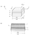
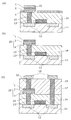
- FIG. 1A is a perspective view schematically showing a configuration of a main part of a storage unit of the nonvolatile memory element according to the first embodiment of the present invention.
- FIG. 1B is a cross-sectional view showing a cross section taken along the line II of FIG.
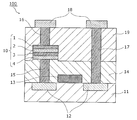
- FIG. 2 is a cross-sectional view showing a specific configuration of the nonvolatile memory device equipped with the nonvolatile memory element according to the first embodiment of the present invention.
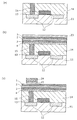
- 3A to 3C are cross-sectional views illustrating steps of the method for manufacturing the nonvolatile memory device according to the first embodiment of the present invention.
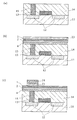
- 4A to 4C are cross-sectional views illustrating the steps of the method for manufacturing the nonvolatile memory device according to the first embodiment of the present invention.
- FIG. 1A is a perspective view schematically showing a configuration of a main part of a storage unit of the nonvolatile memory element according to the first embodiment of the present invention.
- FIG. 1B is a cross-sectional view showing a
- FIG. 5A is a perspective view schematically showing a configuration of a main part of the storage unit of the nonvolatile memory element according to the second embodiment of the present invention.
- FIG. 5B is a cross-sectional view showing a cross section taken along the line II-II in FIG.
- FIG. 6 is a cross-sectional view showing a specific configuration of a nonvolatile memory device equipped with a nonvolatile element according to the second embodiment of the present invention.
- 7A to 7C are cross-sectional views illustrating the steps of the method for manufacturing the nonvolatile memory device according to the second embodiment of the present invention.
- 8A to 8C are cross-sectional views illustrating the steps of the method for manufacturing the nonvolatile memory device according to the second embodiment of the present invention.
- FIG. 9 is a cross-sectional view of the main part showing the configuration of a conventional nonvolatile memory element.
- the nonvolatile memory element 10 of the present invention includes a connection electrode layer 4 and an upper electrode layer 1 formed above the lower electrode layer 3. .
- a resistance change layer 2 is formed between the lower electrode layer 3 and the upper electrode layer 1.
- FIG. 2 is a cross-sectional view showing a specific configuration of the nonvolatile memory device 100 on which the nonvolatile memory element 10 according to the first embodiment of the present invention is mounted.
- a large number of nonvolatile memory elements are formed on the substrate, but only one nonvolatile memory element is shown here for the sake of simplification of the drawing.
- a part of the diagram is enlarged for easy understanding.
- a gate layer 13 and a source and drain layer 12 are formed on a substrate 11, and a first connected to the source and drain layer 12 is formed.
- the contact 15 is formed so as to penetrate the first insulating layer 14.
- the connection electrode layer 4 of the nonvolatile memory element 10 is connected to the first contact. That is, the nonvolatile memory element 10 in which the connection electrode layer 4, the lower electrode layer 3, the resistance change layer 2, and the upper electrode layer 1 are formed on the first contact is formed.
- a second insulating layer 19 is formed so as to cover the gate layer 13, the source / drain layer 12, the first contact 15, and the nonvolatile memory element 10.
- the wiring 18 is formed in a predetermined shape on the upper surface of the second insulating layer 19. Then, a second contact 16 and a third contact 17 are formed so as to penetrate the second insulating layer 19 and the first insulating layer 14, and the upper electrode of the nonvolatile memory element 10 is formed by the second contact 16.
- the layer 1 is connected to the wiring 18, and the source and drain layers 12 are connected to the wiring 18 by the third contact 17.
- the first predetermined resistance value and the second predetermined resistance value are associated with, for example, two values of binary data.
- binary data can be written into the nonvolatile memory element 10 by applying the first or second predetermined electrical pulse to the resistance change layer 2. Further, by supplying a voltage or current that does not change the resistance value of the resistance change layer 2 to the nonvolatile memory element 10 and detecting the resistance value, the binary value written in the nonvolatile memory element 10 is detected. Data can be read out.
- the resistance change layer 2 disposed between the lower electrode layer 3 and the upper electrode layer 1 functions as a memory unit.
- a nonvolatile memory element 10 is connected to a transistor (voltage or current supply switch) composed of a gate layer 13, a source and a drain layer 12, and the nonvolatile memory element 10 is controlled by this transistor.
- a transistor voltage or current supply switch
- binary data can be written to the nonvolatile memory element 10 as described above, and further, the binary data written to the nonvolatile memory element 10 can be written as described above. Can be read.
- FIGS. 3A to 3C and FIGS. 4A to 4C show the steps of the method for manufacturing the nonvolatile memory element 10 and the nonvolatile memory device 100 according to the first embodiment of the present invention. It is sectional drawing.
- the first insulating layer 14 is formed, and the first insulating layer 14 is formed.
- a first contact 15 that penetrates through and connects to the source and drain layers 12 is formed.
- connection electrode layer 4, the lower electrode layer 3, and the non-volatile memory element 10 are formed on the first insulating layer 14 so as to cover the first contact 15.
- the resistance change layer 2, the upper electrode layer 1, and the mask layer 23 are formed in this order.
- connection electrode layer 4 exposed in the three-layer etching step is removed by a dry etching process.
- the upper electrode layer 1, the resistance change layer 2, the lower electrode layer 3, and the connection electrode layer 4 are formed, and the upper electrode layer 1, the resistance change layer 2, and the lower electrode layer 3 are connected.
- the non-volatile memory element 10 in which the side surfaces of the electrode layer 4 have the same surface shape is formed.
- a second insulating layer 19 is further formed so as to cover the nonvolatile memory element 10, penetrates the second insulating layer 19, and the upper part of the nonvolatile memory element 10.
- a third contact 17 that penetrates through the second contact 16, the second insulating layer 19, and the first insulating layer 14 connected to the electrode layer 1 and connects to the source and drain layers 12 is formed.
- wirings 18 connected to the second contact 16 and the third contact 17 are formed on the upper surface of the first insulating layer 14.
- the nonvolatile memory device 100 on which the nonvolatile memory element 10 shown in FIG. 2 is mounted is manufactured.
- this nonvolatile memory element 10 for example, a nonvolatile memory device having a configuration of 1 transistor / 1 nonvolatile memory can be manufactured.
- the TiAlN of the mask layer 23 is etched using a mixed gas of Ar, Cl, and trifluoromethane (CHF 3 ) using the resist film 24 as a mask.
- the etching rate of Pt is 7.5 times that of TiAlN
- the etching rate of TaO x is about 1 time that of TiAlN
- the etching rate of TaN is about 10 times that of TiAlN. It is.
- TiAlN as a mask layer is 100 nm
- the connection electrode layer 4 should be set to 70 nm because it should be 51 nm or more.
- the TiAlN of the mask layer 23 is removed using a mixed gas of Ar, Cl, and CHF 3 , and at the same time, the TiAlN of the connection electrode layer 4 is etched.
- the first insulating layer 14 is stably etched by about 40 nm because of a slight over-etching. Further, by optimizing the overetch amount, the etch amount of the first insulating layer 14 can be reduced to 5 nm or less.
- the upper region width 101 (shown in FIG. 1) where the resistance change layer 2 and the upper electrode layer 1 are in contact is 491 nm
- the lower region width 102 where the resistance change layer 2 and the lower electrode layer 3 are in contact is 512 nm.
- the dimensional error from the designed values of the upper region width 101 and the lower region width 102 can be within 12 nm
- the area of the nonvolatile memory element 10 is the designed value. To a shape shift within 5%.
- the charge of the etching plasma applied from the upper electrode side flows through the resistance change layer and flows to the lower electrode side.
- This charge causes oxygen and vacancies in the resistance change layer to move, disturbing the oxygen concentration distribution, and causes characteristic deterioration unique to the resistance change memory device that causes variations in initial operation and operation characteristics.
- a material having a higher standard electrode potential (for example, Pt or Ir) and a lower material (for example, TaN or Al) than the standard electrode potential of the metal included in the resistance change layer 2 are disposed on the upper electrode and the lower electrode, respectively.
- the resistance can be selectively changed near the interface with the electrode having a high standard electrode potential, and stable operation can be realized.
- connection electrode layer 4 may have a laminated structure of TiAlN and TiN. In this case, the same effect can be obtained even when TiAlN is 50 nm and TiN is 20 nm in the above structure. .
- the mask layer 23 is not limited to TiAlN, and the etching rate of the connection electrode layer 4 and the mask layer 23 is lower when the upper electrode layer 1 or the lower electrode layer 3 is formed by etching. As long as the material has an etching rate of about 7.5 times or more than 7.5 times the etching rate, the combination of the above materials is not limited. For example, even when TiN is used as the mask layer 23, the same effect can be obtained.
- the thickness (t ce ) of the connection electrode layer is set to the thickness (t ue ) of the upper electrode layer from the thickness (t m ) of the mask layer.
- etching rate of the mask layer at the time of the three-layer etching step is obtained by dividing the film thickness (t r ) of the change layer by the etching rate (ER r ) of the resistance change layer at the time of the three-layer etching step.
- connection electrode layer may be determined so that this relationship is established.
- t ue1 , t r1 , and t le1 are converted into the thickness of the mask layer by converting the thickness of the upper electrode layer, the thickness of the variable resistance layer, and the thickness of the lower electrode layer, respectively, in consideration of the etch rate.
- the equivalent film thickness. Therefore, t m1 is the remaining film thickness of the mask layer after completion of the three-layer etching process. Furthermore, t m2 is converted to the thickness of the connection electrode layer in consideration of the etch rate when the remaining mask layer is removed at the same time as the connection electrode layer.
- the relational expression is that the first condition is that when all the mask layers remaining after the three-layer etching process are removed, the connection electrode layer is not lost first.
- tue2 is the etching rate of the remaining thickness of the upper electrode layer when the connection electrode layer is further etched after removing the mask layer remaining after the completion of the three-layer etching process. Is a converted film thickness converted to the thickness of the connection electrode layer. Therefore, the relationship of the right side of the formula (1) is that the upper electrode layer is not lost first when all the connection electrode layers are removed after removing all the mask layers remaining after the end of the three-layer etching process. It is a relational expression as the second condition. In an actual process, in order to remove all the connection electrode layers in the region exposed in the three-layer etching step, overetching is necessary, and at this time, the first insulating layer 14 is slightly etched. Further, since a contact plug is formed in the upper electrode layer in order to make contact with the wiring with the upper layer, the remaining film thickness of the upper electrode layer needs to be about 15 to 20 nm or more.
- FIG. 5A is a perspective view schematically showing a configuration of a main part of the storage unit of the nonvolatile memory element 20 according to the second embodiment of the present invention
- FIG. 2 is a cross-sectional view showing a cross section taken along line II-II.
- the nonvolatile memory element 20 includes an upper electrode layer 1 formed above the connection electrode layer 4.
- a resistance change layer 2 is formed between the connection electrode layer and the upper electrode layer 1.
- FIG. 6 is a cross-sectional view showing a specific configuration of the nonvolatile memory device 200 on which the nonvolatile memory element 20 according to the second embodiment is mounted. Therefore, the upper electrode layer 1 formed above the connection electrode layer 4 is provided. Between these connection electrode layers and the upper electrode layer 1, a nonvolatile memory element 20 having a resistance change layer 2 is formed. In a normal case, a large number of nonvolatile memory elements are formed on the substrate, but only one nonvolatile memory element is shown here for the sake of simplification of the drawing. In addition, a part of the diagram is enlarged for easy understanding.
- the other configuration of the nonvolatile memory device 200 is the same as that of the nonvolatile memory device 100, the same reference numerals are given and description thereof is omitted.
- FIGS. 8 (a) to 8 (c) are cross sections showing the steps of the method for manufacturing the nonvolatile memory element 20 and the nonvolatile memory device 200 according to the second embodiment of the present invention. Although it is a figure, it is the same as that of the manufacturing method of the non-volatile memory element 10 and the non-volatile memory device 100 mentioned above except for the following point.
- the difference from the manufacturing method of the nonvolatile memory element 10 and the nonvolatile memory device 100 is that the nonvolatile material is nonvolatile on the first insulating layer 14 so as to cover the first contact 15 in the step shown in FIG.
- the connection electrode layer 4, the resistance change layer 2, the upper electrode layer 1, and the mask layer 23 constituting the memory element 20 are formed in this order. It is desirable that the mask layer 23 and the connection electrode layer 4 have the same etching rate.
- both TiAlN were used.
- the film thicknesses were set to 100 nm and 70 nm, respectively, as in the first embodiment.
- the upper electrode layer 1 and the resistance change layer 2 are formed into a predetermined shape by a single etching using the mask layer 23 as a mask by a dry etching process. To do. This process is called a two-layer etching process.
- the region exposed in the two-layer etching step of the connection electrode layer 4 is removed by a dry etching process.
- the mask layer 23 is also removed at the same time, the upper electrode layer 1, the resistance change layer 2 and the connection electrode layer 4 are formed, and the side surfaces of the upper electrode layer 1, the resistance change layer 2 and the connection electrode layer 4 are the same surface.
- a non-volatile memory element 20 having a shape is formed.
- the above-described materials and film thicknesses may be used for the upper electrode layer 1, the resistance change layer 2, and the connection electrode layer 4, respectively. Similar to the nonvolatile memory element 10 and the nonvolatile memory device 100, it is possible to obtain an effect that a dimensional shift can be reduced.
- the thickness (t ce ) of the connection electrode layer is set to the thickness (t ue ) of the upper electrode layer from the thickness (t m ) of the mask layer.
- connection electrode layer Divided by the etch rate (ER m @ 2) of the mask layer at the time when the step of removing the area exposed in the layer etching process, in removing the mask layer, the second layer etching step of the connection electrode layer
- T m to the value obtained by dividing the film thickness (t ue ) of the upper electrode layer by the etching rate (ER ue ) of the upper electrode layer at the time of the two-layer etching process.
- the film thickness ( t ue ⁇ ER m1 / ER ue ) multiplied by the etching rate (ER m1 ) of the mask layer and the film thickness (t r ) of the resistance change layer at the time of the two-layer etching step
- a process of removing the region exposed in the two-layer etching process of the connection electrode layer Divided by the etch rate (ER ue2) of said upper electrode layer at the time when the, when removing the mask layer, when the step of removing the exposed regions in the two-layer etching step of the connection electrode layer
- connection electrode layer may be determined so that this relationship is established.
- tue2 is the etching rate of the remaining film thickness of the upper electrode layer when the connection electrode layer is further etched after removing the mask layer remaining after the completion of the two-layer etching process. Is a converted film thickness converted to the thickness of the connection electrode layer. Therefore, the relationship of the right side of the formula (1) is that the upper electrode layer is not lost when the connection electrode layer is completely removed after removing the mask layer remaining after the end of the two-layer etching process. It is a relational expression as the second condition. In an actual process, in order to remove all the connection electrode layers in the region exposed in the three-layer etching step, overetching is necessary, and at this time, the first insulating layer 14 is slightly etched. Further, since a contact plug is formed in the upper electrode layer in order to make contact with the wiring with the upper layer, the remaining film thickness of the upper electrode layer needs to be about 15 to 20 nm or more.
- the nonvolatile memory element and the nonvolatile memory device of the present invention are capable of high-speed operation and have stable rewriting characteristics, and various electronic devices such as digital home appliances, memory cards, portable telephones, and personal computers. It is useful as a non-volatile memory element used in the above.
Abstract
Description
2008年5月8日に出願された出願番号2008-121948の日本出願の明細書、図面および特許請求の範囲における開示は、その全体を、参照用として、本願に取り込む。
図1(a)は本発明の実施の形態に係る不揮発性記憶素子10の記憶部の要部の構成を模式的に示す斜視図であり、図1(b)は、図1(a)のI-I線に沿った断面を示す断面図である。
tm2<tce<tm2+tue2 (1)
の関係が成り立つよう、接続電極層の膜厚(tce)を決定すればよい。
図5(a)は本発明の第2の実施の形態に係る不揮発性記憶素子20の記憶部の要部の構成を模式的に示す斜視図であり、図5(b)は図5(a)のII-II線に沿った断面を示す断面図である。
tm2<tce<tm2+tue2 (2)
の関係が成り立つよう、接続電極層の膜厚(tce)を決定すればよい。
2 抵抗変化層
3 下部電極層
4 接続電極層
10、20 不揮発性記憶素子
11 基板
12 ソースおよびドレイン層
13 ゲート層
14 第1の絶縁層
15 第1のコンタクト
16 第2のコンタクト
17 第3のコンタクト
18 配線
19 第2の絶縁層
23 マスク層
24 レジスト膜
100、200 不揮発性記憶装置
101 上部領域幅
102 下部領域幅
920 半導体基板
921a ソース領域
921b ドレイン領域
922 ゲート絶縁層
923 ゲート電極
924 層間絶縁膜
925 コンタクトプラグ
931 下部電極
932 抵抗体
933 上部電極
Claims (20)
- 導電性を有する接続電極層と、非貴金属の窒化物からなりかつ導電性を有する下部電極層と、前記下部電極層より上方に形成されかつ貴金属からなる上部電極層と、前記下部電極層と前記上部電極層との間に介在させ、前記下部電極層および前記上部電極層間に与えられる電気的信号に基づいて可逆的に抵抗値が変化する抵抗変化層とを備えた不揮発性記憶素子の製造方法において、
前記接続電極層、前記下部電極層、前記抵抗変化層、前記上部電極層、およびマスク層をこの順に堆積させる工程と、
前記マスク層をレジスト膜をマスクとして所定の形状に形成する工程と、
前記所定の形状に形成されたマスク層をマスクとして前記上部電極層、前記抵抗変化層、および前記下部電極層をエッチングで所定の形状に形成する3層エッチング工程と、
前記マスク層と、前記接続電極層の前記3層エッチング工程で露出された領域とを同時に除去する工程と
を含む不揮発性記憶素子の製造方法。 - 前記3層エッチング工程において、前記マスク層をマスクとして前記上部電極層、前記抵抗変化層、および前記下部電極層を1回のエッチングで所定の形状に形成する
ことを特徴とする請求項1に記載の不揮発性記憶素子の製造方法。 - 前記マスク層の前記3層エッチング工程の時のエッチングレートは、少なくとも前記3層エッチング工程の時の前記レジスト膜のエッチングレートより小さい
ことを特徴とする請求項1または請求項2に記載の不揮発性記憶素子の製造方法。 - 前記上部電極層はPtまたはIrからなり、前記下部電極層はTaNからなり、前記接続電極層はTiAlNからなる
ことを特徴とする請求項1から請求項3のいずれか1項に記載の不揮発性記憶素子の製造方法。 - 導電性を有する接続電極層と、前記接続電極層より上方に形成されかつ貴金属からなる上部電極層と、前記接続電極層と前記上部電極層との間に介在させ、前記接続電極層および前記上部電極層間に与えられる電気的信号に基づいて可逆的に抵抗値が変化する抵抗変化層とを備えた不揮発性記憶素子の製造方法において、
前記接続電極層、前記抵抗変化層、前記上部電極層、およびマスク層をこの順に堆積させる工程と、
前記マスク層をレジスト膜をマスクとして所定の形状に形成する工程と、
前記所定の形状に形成されたマスク層をマスクとして前記上部電極層、および前記抵抗変化層をエッチングで所定の形状に形成する2層エッチング工程と、
前記マスク層と前記接続電極層の前記2層エッチング工程で露出された領域とを同時に除去する工程と
を含む不揮発性記憶素子の製造方法。 - 前記2層エッチング工程において、
前記マスク層をマスクとして前記上部電極層、および前記抵抗変化層を1回のエッチングで所定の形状に形成する
ことを特徴とする請求項5に記載の不揮発性記憶素子の製造方法。 - 前記マスク層の前記2層エッチング工程の時のエッチングレートは、少なくとも前記2層エッチング工程の時の前記レジスト膜のエッチングレートより小さい
ことを特徴とする請求項5または請求項6に記載の不揮発性記憶素子の製造方法。 - 前記上部電極層はPtまたはIrからなり、前記接続電極層はTiAlNからなる
ことを特徴とする請求項5から請求項7のいずれか1項に記載の不揮発性記憶素子の製造方法。 - 前記接続電極層は前記マスク層と同一のエッチングレートを有する
ことを特徴とする請求項1から請求項8のいずれか1項に記載の不揮発性記憶素子の製造方法。 - 前記接続電極層は前記マスク層と同一の材料により構成されている
ことを特徴とする請求項1から請求項9のいずれか1項に記載の不揮発性記憶素子の製造方法。 - 半導体基板と、前記半導体基板上に形成された、互いに交差するように配列された複数のワード線および複数のビット線、前記複数のワード線および複数のビット線の交点に対応してそれぞれ設けられた複数のトランジスタ、並びに前記複数のトランジスタに一対一で対応して設けられた複数の不揮発性記憶素子とを備え、
前記不揮発性記憶素子のそれぞれは、導電性を有する接続電極層と、非貴金属の窒化物からなりかつ導電性を有する下部電極層と、前記下部電極層より上方に形成されかつ貴金属からなる上部電極層と、前記下部電極層と前記上部電極層との間に介在させ、前記下部電極層および前記上部電極層間に与えられる電気的信号に基づいて可逆的に抵抗値が変化する抵抗変化層とを備えた不揮発性記憶装置の製造方法において、
前記接続電極層、前記下部電極層、前記抵抗変化層、前記上部電極層、およびマスク層をこの順に堆積させる工程と、
前記マスク層をレジスト膜をマスクとして所定の形状に形成する工程と、
前記所定の形状に形成されたマスク層をマスクとして前記上部電極層、前記抵抗変化層、および前記下部電極層をエッチングで所定の形状に形成する3層エッチング工程と、
前記マスク層と前記接続電極層の前記3層エッチング工程で露出された領域とを同時に除去する工程と、
前記接続電極層及び前記上部電極層と電気的に接続される前記トランジスタおよび半導体集積回路を前記基板に形成する工程と
を含む不揮発性記憶装置の製造方法。 - 前記3層エッチング工程において、前記マスク層をマスクとして前記上部電極層、前記抵抗変化層、および前記下部電極層を1回のエッチングで所定の形状に形成する
ことを特徴とする請求項11に記載の不揮発性記憶装置の製造方法。 - 半導体基板と、前記半導体基板上に形成された、互いに交差するように配列された複数のワード線および複数のビット線、前記複数のワード線および複数のビット線の交点に対応してそれぞれ設けられた複数のトランジスタ、並びに前記複数のトランジスタに一対一で対応して設けられた複数の不揮発性記憶素子とを備え、
前記不揮発性記憶素子のそれぞれは、導電性を有する接続電極層と、前記接続電極層より上方に形成されかつ貴金属からなる上部電極層と、前記接続電極層と前記上部電極層との間に介在させ、前記接続電極層および前記上部電極間に与えられる電気的信号に基づいて可逆的に抵抗値が変化する抵抗変化層とを備えた不揮発性記憶装置の製造方法において、
前記接続電極層、前記抵抗変化層、前記上部電極層、およびマスク層をこの順に堆積させる工程と、
前記マスク層をレジスト膜をマスクとして所定の形状に形成する工程と、
前記所定の形状に形成されたマスク層をマスクとして前記上部電極層、および前記抵抗変化層をエッチングで所定の形状に形成する2層エッチング工程と、
前記マスク層と前記接続電極層の前記2層エッチング工程で露出された領域とを同時に除去する工程と、
前記接続電極層及び前記上部電極層と電気的に接続される前記トランジスタおよび半導体集積回路を前記基板に形成する工程と
を含む不揮発性記憶装置の製造方法。 - 前記2層エッチング工程において、前記マスク層をマスクとして前記上部電極層、および前記抵抗変化層を1回のエッチングで所定の形状に形成する
ことを特徴とする請求項13に記載の不揮発性記憶装置の製造方法。 - 非貴金属の窒化物からなりかつ導電性を有する下部電極層と、前記下部電極層より上方に形成されかつ貴金属からなる上部電極層と、前記下部電極層と前記上部電極層との間に介在させ、前記下部電極層および前記上部電極層間に与えられる電気的信号に基づいて可逆的に抵抗値が変化する抵抗変化層と、前記下部電極層の下方に形成され、前記上部電極層および前記下部電極層とは異なる材料からなり、導電性を有する接続電極層とを備え、
前記接続電極層と前記下部電極層と前記抵抗変化層と前記上部電極層の側壁が同一の面を有する
不揮発性記憶素子。 - 前記上部電極層はPtまたはIrからなり、前記下部電極はTaNからなり、前記接続電極層はTiAlNからなる
ことを特徴とする請求項15に記載の不揮発性記憶素子。 - 接続電極層と、前記接続電極層より上方に形成されかつ貴金属からなる上部電極層と、前記接続電極層と前記上部電極層との間に介在させ、前記接続電極層および前記上部電極層間に与えられる電気的信号に基づいて可逆的に抵抗値が変化する抵抗変化層とを備え、
前記接続電極層は導電性を有し、上部電極層とは異なる材料からなり、前記接続電極層と前記抵抗変化層と前記上部電極層の側壁が同一の面を有する
不揮発性記憶素子。 - 前記上部電極層はPtまたはIrからなり、前記接続電極層はTiAlNからなる
ことを特徴とする請求項17に記載の不揮発性記憶素子。 - 前記接続電極層の膜厚は、
前記マスク層の膜厚から、
前記上部電極層の膜厚を、前記3層エッチング工程の時の前記上部電極層のエッチングレートで割った値に、前記3層エッチング工程の時の前記マスク層のエッチングレートを掛けた膜厚と、
前記抵抗変化層の膜厚を、前記3層エッチング工程の時の前記抵抗変化層のエッチングレートで割った値に、前記3層エッチング工程の時の前記マスク層のエッチングレートを掛けた膜厚と、
前記下部電極層の膜厚を、前記3層エッチング工程の時の前記下部電極層のエッチングレートで割った値に、前記3層エッチング工程の時の前記マスク層のエッチングレートを掛けた膜厚と
を引いた膜厚を、前記マスク層を除去する際に、前記接続電極層の前記3層エッチング工程で露出された領域を除去する工程の時の前記マスク層のエッチングレートで割った値に、前記マスク層を除去する際に、前記接続電極層の前記3層エッチング工程で露出された領域を除去する工程の時の前記接続電極層のエッチングレートを掛けた膜厚より厚く、
前記マスク層の膜厚から、
前記上部電極層の膜厚を、前記3層エッチング工程の時の前記上部電極層のエッチングレートで割った値に、前記3層エッチング工程の時の前記マスク層のエッチングレートを掛けた膜厚と、
前記抵抗変化層の膜厚を、前記3層エッチング工程の時の前記抵抗変化層のエッチングレートで割った値に、前記3層エッチング工程の時の前記マスク層のエッチングレートを掛けた膜厚と、
前記下部電極層の膜厚を、前記3層エッチング工程の時の前記下部電極層のエッチングレートで割った値に、前記3層エッチング工程の時の前記マスク層のエッチングレートを掛けた膜厚と
を引いた膜厚を、前記マスク層を除去する際に、前記接続電極層の前記3層エッチング工程で露出された領域を除去する工程の時の前記マスク層のエッチングレートで割った値に、前記マスク層を除去する際に、前記接続電極層の前記3層エッチング工程で露出された領域を除去する工程の時の前記接続電極層のエッチングレートを掛けた膜厚と、
前記上部電極層の膜厚を、前記マスク層を除去する際に、前記接続電極層の前記3層エッチング工程で露出された領域を除去する工程の時の前記上部電極層のエッチングレートで割った値に、前記マスク層と前記接続電極層の前記3層エッチング工程で露出された領域とを同時に除去する工程の時の前記接続電極層のエッチングレートを掛けた膜厚と
を足した膜厚より薄い
ことを特徴とする請求項15または請求項16に記載の不揮発性記憶素子。 - 前記接続電極層の膜厚は、
前記マスク層の膜厚から、
前記上部電極層の膜厚を、前記2層エッチング工程の時の前記上部電極層のエッチングレートで割った値に、前記2層エッチング工程の時の前記マスク層のエッチングレートを掛けた膜厚と、
前記抵抗変化層の膜厚を、前記2層エッチング工程の時の前記抵抗変化層のエッチングレートで割った値に、前記2層エッチング工程の時の前記マスク層のエッチングレートを掛けた膜厚と
を引いた膜厚を、前記マスク層を除去する際に、前記接続電極層の前記抵抗変化層に覆われていない領域を除去する工程の時の前記マスク層のエッチングレートで割った値に、前記マスク層を除去する際に、前記接続電極層の前記抵抗変化層に覆われていない領域を除去する工程の時の前記接続電極層のエッチングレートを掛けた膜厚より厚く、
前記マスク層の膜厚から、
前記上部電極層の膜厚を、前記2層エッチング工程の時の前記上部電極層のエッチングレートで割った値に、前記2層エッチング工程の時の前記マスク層のエッチングレートを掛けた膜厚と、
前記抵抗変化層の膜厚を、前記2層エッチング工程の時の前記抵抗変化層のエッチングレートで割った値に、前記2層エッチング工程の時の前記マスク層のエッチングレートを掛けた膜厚と
を引いた膜厚を、前記マスク層を除去する際に、前記接続電極層の前記2層エッチング工程で露出された領域を除去する工程の時の前記マスク層のエッチングレートで割った値に、前記マスク層を除去する際に、前記接続電極層の前記2層エッチング工程で露出された領域を除去する工程の時の前記接続電極層のエッチングレートを掛けた膜厚と、
前記上部電極層の膜厚を、前記マスク層を除去する際に、前記接続電極層の前記2層エッチング工程で露出された領域を除去する工程の時の前記上部電極層のエッチングレートで割った値に、前記マスク層と前記接続電極層の前記2層エッチング工程で露出された領域とを同時に除去する工程の時の前記接続電極層のエッチングレートを掛けた膜厚と
を足した膜厚より薄い
ことを特徴とする請求項17または請求項18に記載の不揮発性記憶素子。
Priority Applications (3)
| Application Number | Priority Date | Filing Date | Title |
|---|---|---|---|
| US12/669,812 US7981760B2 (en) | 2008-05-08 | 2009-05-07 | Method for manufacturing nonvolatile storage element and method for manufacturing nonvolatile storage device |
| JP2010511019A JP5074583B2 (ja) | 2008-05-08 | 2009-05-07 | 不揮発性記憶素子の製造方法、および不揮発性記憶装置の製造方法 |
| CN200980000536.0A CN101796640A (zh) | 2008-05-08 | 2009-05-07 | 非易失性存储元件、非易失性存储装置、以及其制造方法 |
Applications Claiming Priority (2)
| Application Number | Priority Date | Filing Date | Title |
|---|---|---|---|
| JP2008121948 | 2008-05-08 | ||
| JP2008-121948 | 2008-05-08 |
Publications (1)
| Publication Number | Publication Date |
|---|---|
| WO2009136493A1 true WO2009136493A1 (ja) | 2009-11-12 |
Family
ID=41264550
Family Applications (1)
| Application Number | Title | Priority Date | Filing Date |
|---|---|---|---|
| PCT/JP2009/001994 WO2009136493A1 (ja) | 2008-05-08 | 2009-05-07 | 不揮発性記憶素子、及び、不揮発性記憶素子又は不揮発性記憶装置の製造方法 |
Country Status (4)
| Country | Link |
|---|---|
| US (1) | US7981760B2 (ja) |
| JP (1) | JP5074583B2 (ja) |
| CN (1) | CN101796640A (ja) |
| WO (1) | WO2009136493A1 (ja) |
Cited By (3)
| Publication number | Priority date | Publication date | Assignee | Title |
|---|---|---|---|---|
| WO2012001978A1 (ja) * | 2010-07-01 | 2012-01-05 | パナソニック株式会社 | 不揮発性記憶素子及びその製造方法 |
| JPWO2012140887A1 (ja) * | 2011-04-14 | 2014-07-28 | パナソニック株式会社 | 不揮発性記憶素子およびその製造方法 |
| CN112054117A (zh) * | 2019-06-05 | 2020-12-08 | 联华电子股份有限公司 | 存储器元件的结构及其制造方法 |
Families Citing this family (5)
| Publication number | Priority date | Publication date | Assignee | Title |
|---|---|---|---|---|
| JP5438707B2 (ja) | 2011-03-04 | 2014-03-12 | シャープ株式会社 | 可変抵抗素子及びその製造方法、並びに、当該可変抵抗素子を備えた不揮発性半導体記憶装置 |
| WO2012169195A1 (ja) * | 2011-06-10 | 2012-12-13 | 株式会社アルバック | 抵抗変化素子及びその製造方法 |
| WO2013054506A1 (ja) * | 2011-10-11 | 2013-04-18 | パナソニック株式会社 | 半導体記憶素子の製造方法 |
| US8658511B1 (en) | 2012-12-20 | 2014-02-25 | Intermolecular, Inc. | Etching resistive switching and electrode layers |
| JP2014127566A (ja) * | 2012-12-26 | 2014-07-07 | Panasonic Corp | 不揮発性記憶装置の製造方法および不揮発性記憶装置 |
Citations (3)
| Publication number | Priority date | Publication date | Assignee | Title |
|---|---|---|---|---|
| JP2003273330A (ja) * | 2002-03-15 | 2003-09-26 | Matsushita Electric Ind Co Ltd | 容量素子の製造方法 |
| JP2003318371A (ja) * | 2002-01-31 | 2003-11-07 | Texas Instruments Inc | 強誘電体メモリセルに関連するキャパシタスタックのエッチング方法 |
| JP2008021750A (ja) * | 2006-07-11 | 2008-01-31 | Matsushita Electric Ind Co Ltd | 抵抗変化素子およびその製造方法、ならびにそれを用いた抵抗変化型メモリ |
Family Cites Families (16)
| Publication number | Priority date | Publication date | Assignee | Title |
|---|---|---|---|---|
| US4138013A (en) * | 1976-08-27 | 1979-02-06 | Parke, Davis & Company | Enteric capsules |
| US4265814A (en) * | 1978-03-24 | 1981-05-05 | Takeda Chemical Industries | Matansinol 3-n-hexadecanoate |
| US4790881A (en) * | 1982-03-26 | 1988-12-13 | Warner-Lambert Company | Molded hydrophilic polymer |
| US4462839A (en) * | 1983-06-16 | 1984-07-31 | Fmc Corporation | Enteric coating for pharmaceutical dosage forms |
| US5330759A (en) * | 1992-08-26 | 1994-07-19 | Sterling Winthrop Inc. | Enteric coated soft capsules and method of preparation thereof |
| US7122207B2 (en) * | 1998-05-22 | 2006-10-17 | Bristol-Myers Squibb Company | High drug load acid labile pharmaceutical composition |
| IL133196A0 (en) * | 1999-11-29 | 2001-03-19 | Yissum Res Dev Co | Gastroretentive controlled release pharmaceutical dosage forms |
| US6566148B2 (en) * | 2001-08-13 | 2003-05-20 | Sharp Laboratories Of America, Inc. | Method of making a ferroelectric memory transistor |
| JP2004273656A (ja) | 2003-03-07 | 2004-09-30 | Taiyo Yuden Co Ltd | Epir素子及びそれを利用した半導体装置 |
| US6955992B2 (en) | 2003-09-30 | 2005-10-18 | Sharp Laboratories Of America, Inc. | One mask PT/PCMO/PT stack etching process for RRAM applications |
| US6972985B2 (en) | 2004-05-03 | 2005-12-06 | Unity Semiconductor Corporation | Memory element having islands |
| WO2005117021A1 (en) | 2004-05-03 | 2005-12-08 | Unity Semiconductor Corporation | Non-volatile programmable memory |
| US7169637B2 (en) | 2004-07-01 | 2007-01-30 | Sharp Laboratories Of America, Inc. | One mask Pt/PCMO/Pt stack etching process for RRAM applications |
| KR100682895B1 (ko) | 2004-11-06 | 2007-02-15 | 삼성전자주식회사 | 다양한 저항 상태를 지닌 저항체를 이용한 비휘발성메모리 소자 및 그 작동 방법 |
| CN101111929B (zh) * | 2005-01-28 | 2010-05-19 | 株式会社爱发科 | 电容元件的制造方法以及蚀刻方法 |
| US20060190704A1 (en) * | 2005-02-24 | 2006-08-24 | International Business Machines Corporation | Apparatus for increasing addressability of registers within a processor |
-
2009
- 2009-05-07 US US12/669,812 patent/US7981760B2/en active Active
- 2009-05-07 WO PCT/JP2009/001994 patent/WO2009136493A1/ja active Application Filing
- 2009-05-07 JP JP2010511019A patent/JP5074583B2/ja active Active
- 2009-05-07 CN CN200980000536.0A patent/CN101796640A/zh active Pending
Patent Citations (3)
| Publication number | Priority date | Publication date | Assignee | Title |
|---|---|---|---|---|
| JP2003318371A (ja) * | 2002-01-31 | 2003-11-07 | Texas Instruments Inc | 強誘電体メモリセルに関連するキャパシタスタックのエッチング方法 |
| JP2003273330A (ja) * | 2002-03-15 | 2003-09-26 | Matsushita Electric Ind Co Ltd | 容量素子の製造方法 |
| JP2008021750A (ja) * | 2006-07-11 | 2008-01-31 | Matsushita Electric Ind Co Ltd | 抵抗変化素子およびその製造方法、ならびにそれを用いた抵抗変化型メモリ |
Cited By (7)
| Publication number | Priority date | Publication date | Assignee | Title |
|---|---|---|---|---|
| WO2012001978A1 (ja) * | 2010-07-01 | 2012-01-05 | パナソニック株式会社 | 不揮発性記憶素子及びその製造方法 |
| JP5436669B2 (ja) * | 2010-07-01 | 2014-03-05 | パナソニック株式会社 | 不揮発性記憶素子及びその製造方法 |
| US8785238B2 (en) | 2010-07-01 | 2014-07-22 | Panasonic Corporation | Nonvolatile memory element and method for manufacturing same |
| JPWO2012140887A1 (ja) * | 2011-04-14 | 2014-07-28 | パナソニック株式会社 | 不揮発性記憶素子およびその製造方法 |
| JP5636092B2 (ja) * | 2011-04-14 | 2014-12-03 | パナソニック株式会社 | 不揮発性記憶素子およびその製造方法 |
| US8921200B2 (en) | 2011-04-14 | 2014-12-30 | Panasonic Corporation | Nonvolatile storage element and method of manufacturing thereof |
| CN112054117A (zh) * | 2019-06-05 | 2020-12-08 | 联华电子股份有限公司 | 存储器元件的结构及其制造方法 |
Also Published As
| Publication number | Publication date |
|---|---|
| US7981760B2 (en) | 2011-07-19 |
| JPWO2009136493A1 (ja) | 2011-09-08 |
| US20100190313A1 (en) | 2010-07-29 |
| JP5074583B2 (ja) | 2012-11-14 |
| CN101796640A (zh) | 2010-08-04 |
Similar Documents
| Publication | Publication Date | Title |
|---|---|---|
| JP5074583B2 (ja) | 不揮発性記憶素子の製造方法、および不揮発性記憶装置の製造方法 | |
| JP5468087B2 (ja) | 不揮発性記憶素子及び不揮発性記憶装置 | |
| US9214628B2 (en) | Nonvolatile memory element, nonvolatile memory device, and manufacturing method for the same | |
| JP4948688B2 (ja) | 抵抗変化型不揮発性記憶素子、抵抗変化型不揮発性記憶装置及び抵抗変化型不揮発性記憶素子の製造方法 | |
| US8437173B2 (en) | Nonvolatile memory element, manufacturing method thereof, design support method therefor, and nonvolatile memory device | |
| JP5636081B2 (ja) | 不揮発性記憶装置およびその製造方法 | |
| JP4688979B2 (ja) | 抵抗変化型素子および抵抗変化型記憶装置 | |
| JP5036909B2 (ja) | 抵抗変化型素子及びその製造方法 | |
| JP4971522B2 (ja) | 不揮発性記憶装置及びその製造方法 | |
| JP5110088B2 (ja) | 抵抗変化素子とその製造方法、及び抵抗変化素子を用いた半導体記憶装置 | |
| JP5571833B2 (ja) | 不揮発性記憶素子及び不揮発性記憶素子の製造方法 | |
| JP2010251352A (ja) | 不揮発性記憶素子及びその製造方法 | |
| JP2009071304A (ja) | 抵抗変化型メモリ素子及びその形成方法 | |
| US20140077149A1 (en) | Resistance memory cell, resistance memory array and method of forming the same | |
| US11211555B2 (en) | Memory device and a method for forming the memory device | |
| JP5555821B1 (ja) | 不揮発性記憶素子及びその製造方法 | |
| JP5232935B2 (ja) | 抵抗変化素子の製造方法 | |
| US9142773B2 (en) | Variable resistance nonvolatile memory element and method of manufacturing the same | |
| US20210408119A1 (en) | Non-volatile storage device and method of manufacturing the same | |
| JP5338236B2 (ja) | 不揮発性記憶素子およびその製造方法、並びにその不揮発性記憶素子を用いた不揮発性記憶装置およびその製造方法 | |
| JP2009141275A (ja) | 抵抗変化素子、これを用いた記憶装置、及びそれらの作製方法 | |
| JP2015146343A (ja) | 不揮発性記憶装置およびその製造方法 |
Legal Events
| Date | Code | Title | Description |
|---|---|---|---|
| WWE | Wipo information: entry into national phase |
Ref document number: 200980000536.0 Country of ref document: CN |
|
| WWE | Wipo information: entry into national phase |
Ref document number: 2010511019 Country of ref document: JP |
|
| 121 | Ep: the epo has been informed by wipo that ep was designated in this application |
Ref document number: 09742618 Country of ref document: EP Kind code of ref document: A1 |
|
| WWE | Wipo information: entry into national phase |
Ref document number: 12669812 Country of ref document: US |
|
| NENP | Non-entry into the national phase |
Ref country code: DE |
|
| 122 | Ep: pct application non-entry in european phase |
Ref document number: 09742618 Country of ref document: EP Kind code of ref document: A1 |