JP5110088B2 - 抵抗変化素子とその製造方法、及び抵抗変化素子を用いた半導体記憶装置 - Google Patents
抵抗変化素子とその製造方法、及び抵抗変化素子を用いた半導体記憶装置 Download PDFInfo
- Publication number
- JP5110088B2 JP5110088B2 JP2009544535A JP2009544535A JP5110088B2 JP 5110088 B2 JP5110088 B2 JP 5110088B2 JP 2009544535 A JP2009544535 A JP 2009544535A JP 2009544535 A JP2009544535 A JP 2009544535A JP 5110088 B2 JP5110088 B2 JP 5110088B2
- Authority
- JP
- Japan
- Prior art keywords
- film
- electrode
- nickel
- transition metal
- resistance change
- Prior art date
- Legal status (The legal status is an assumption and is not a legal conclusion. Google has not performed a legal analysis and makes no representation as to the accuracy of the status listed.)
- Expired - Fee Related
Links
Images


Classifications
-
- G—PHYSICS
- G11—INFORMATION STORAGE
- G11C—STATIC STORES
- G11C13/00—Digital stores characterised by the use of storage elements not covered by groups G11C11/00, G11C23/00, or G11C25/00
- G11C13/0002—Digital stores characterised by the use of storage elements not covered by groups G11C11/00, G11C23/00, or G11C25/00 using resistive RAM [RRAM] elements
- G11C13/0007—Digital stores characterised by the use of storage elements not covered by groups G11C11/00, G11C23/00, or G11C25/00 using resistive RAM [RRAM] elements comprising metal oxide memory material, e.g. perovskites
-
- H—ELECTRICITY
- H10—SEMICONDUCTOR DEVICES; ELECTRIC SOLID-STATE DEVICES NOT OTHERWISE PROVIDED FOR
- H10B—ELECTRONIC MEMORY DEVICES
- H10B63/00—Resistance change memory devices, e.g. resistive RAM [ReRAM] devices
- H10B63/30—Resistance change memory devices, e.g. resistive RAM [ReRAM] devices comprising selection components having three or more electrodes, e.g. transistors
-
- H—ELECTRICITY
- H10—SEMICONDUCTOR DEVICES; ELECTRIC SOLID-STATE DEVICES NOT OTHERWISE PROVIDED FOR
- H10N—ELECTRIC SOLID-STATE DEVICES NOT OTHERWISE PROVIDED FOR
- H10N70/00—Solid-state devices without a potential-jump barrier or surface barrier, and specially adapted for rectifying, amplifying, oscillating or switching
- H10N70/011—Manufacture or treatment of multistable switching devices
- H10N70/021—Formation of the switching material, e.g. layer deposition
- H10N70/026—Formation of the switching material, e.g. layer deposition by physical vapor deposition, e.g. sputtering
-
- H—ELECTRICITY
- H10—SEMICONDUCTOR DEVICES; ELECTRIC SOLID-STATE DEVICES NOT OTHERWISE PROVIDED FOR
- H10N—ELECTRIC SOLID-STATE DEVICES NOT OTHERWISE PROVIDED FOR
- H10N70/00—Solid-state devices without a potential-jump barrier or surface barrier, and specially adapted for rectifying, amplifying, oscillating or switching
- H10N70/011—Manufacture or treatment of multistable switching devices
- H10N70/061—Patterning of the switching material
- H10N70/063—Patterning of the switching material by etching of pre-deposited switching material layers, e.g. lithography
-
- H—ELECTRICITY
- H10—SEMICONDUCTOR DEVICES; ELECTRIC SOLID-STATE DEVICES NOT OTHERWISE PROVIDED FOR
- H10N—ELECTRIC SOLID-STATE DEVICES NOT OTHERWISE PROVIDED FOR
- H10N70/00—Solid-state devices without a potential-jump barrier or surface barrier, and specially adapted for rectifying, amplifying, oscillating or switching
- H10N70/20—Multistable switching devices, e.g. memristors
-
- H—ELECTRICITY
- H10—SEMICONDUCTOR DEVICES; ELECTRIC SOLID-STATE DEVICES NOT OTHERWISE PROVIDED FOR
- H10N—ELECTRIC SOLID-STATE DEVICES NOT OTHERWISE PROVIDED FOR
- H10N70/00—Solid-state devices without a potential-jump barrier or surface barrier, and specially adapted for rectifying, amplifying, oscillating or switching
- H10N70/801—Constructional details of multistable switching devices
- H10N70/821—Device geometry
- H10N70/826—Device geometry adapted for essentially vertical current flow, e.g. sandwich or pillar type devices
-
- H—ELECTRICITY
- H10—SEMICONDUCTOR DEVICES; ELECTRIC SOLID-STATE DEVICES NOT OTHERWISE PROVIDED FOR
- H10N—ELECTRIC SOLID-STATE DEVICES NOT OTHERWISE PROVIDED FOR
- H10N70/00—Solid-state devices without a potential-jump barrier or surface barrier, and specially adapted for rectifying, amplifying, oscillating or switching
- H10N70/801—Constructional details of multistable switching devices
- H10N70/841—Electrodes
-
- H—ELECTRICITY
- H10—SEMICONDUCTOR DEVICES; ELECTRIC SOLID-STATE DEVICES NOT OTHERWISE PROVIDED FOR
- H10N—ELECTRIC SOLID-STATE DEVICES NOT OTHERWISE PROVIDED FOR
- H10N70/00—Solid-state devices without a potential-jump barrier or surface barrier, and specially adapted for rectifying, amplifying, oscillating or switching
- H10N70/801—Constructional details of multistable switching devices
- H10N70/881—Switching materials
- H10N70/883—Oxides or nitrides
- H10N70/8833—Binary metal oxides, e.g. TaOx
-
- G—PHYSICS
- G11—INFORMATION STORAGE
- G11C—STATIC STORES
- G11C2213/00—Indexing scheme relating to G11C13/00 for features not covered by this group
- G11C2213/10—Resistive cells; Technology aspects
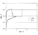
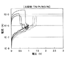
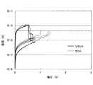
- G11C2213/15—Current-voltage curve
-
- G—PHYSICS
- G11—INFORMATION STORAGE
- G11C—STATIC STORES
- G11C2213/00—Indexing scheme relating to G11C13/00 for features not covered by this group
- G11C2213/30—Resistive cell, memory material aspects
- G11C2213/32—Material having simple binary metal oxide structure
-
- G—PHYSICS
- G11—INFORMATION STORAGE
- G11C—STATIC STORES
- G11C2213/00—Indexing scheme relating to G11C13/00 for features not covered by this group
- G11C2213/30—Resistive cell, memory material aspects
- G11C2213/34—Material includes an oxide or a nitride
-
- G—PHYSICS
- G11—INFORMATION STORAGE
- G11C—STATIC STORES
- G11C2213/00—Indexing scheme relating to G11C13/00 for features not covered by this group
- G11C2213/50—Resistive cell structure aspects
- G11C2213/52—Structure characterized by the electrode material, shape, etc.
-
- G—PHYSICS
- G11—INFORMATION STORAGE
- G11C—STATIC STORES
- G11C2213/00—Indexing scheme relating to G11C13/00 for features not covered by this group
- G11C2213/70—Resistive array aspects
- G11C2213/79—Array wherein the access device being a transistor
Description
K. Kinoshita, et al., "Bias polarity dependent data retention of resistive random access memory consisting of binary transition metal oxide", Applied Physics Letter 89, 103509 (2006) S. Seo, et al., "Reproducible resistance switching in polycriystalline NiO films" Applied Physics Letter, Vol. 85, No. 23, 6 December, 2004 M. Fujimoto, et al., "High-speed Resistive Switching of TiO2/TiN Nano-Crystalline Thin Film", Japanese Journal of Applied Physics, Vol. 45, No. 11, 2006, pp. L310-L312
半導体基板の上方に遷移金属窒化膜を形成する工程と、
前記遷移金属窒化膜上に遷移金属酸化膜を形成する工程と、
前記遷移金属酸化膜上に貴金属又は貴金属酸化物からなる貴金属膜を形成する工程と、
を含む。
複数の選択トランジスタと、
前記選択トランジスタにそれぞれ接続された複数の抵抗変化素子と、
を有し、
前記複数の抵抗変化素子のそれぞれは、
遷移金属窒化物を含む第1の電極と、
貴金属又は貴金属酸化物を含む第2の電極と、
前記第1の電極と前記第2の電極との間に配置された遷移金属酸化膜と、
を備えることを特徴とする。
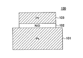
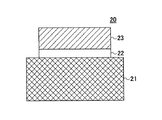
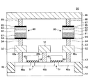
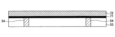
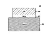
21、31、61、81、91 接地側電極(第1の電極又は下部電極)
31a、81a Ni電極膜
31b、81b NiN電極膜
22、32、62、82、92 抵抗変化膜
23、33、63、83、93 正極側電極(第2の電極又は上部電極)
50 半導体記憶装置(ReRAM)
51 接地線
68 ビット線
Tr 選択トランジスタ
Claims (8)
- 遷移金属窒化物を含む第1の電極と、
貴金属又は貴金属酸化物を含む第2の電極と、
前記第1の電極と前記第2の電極との間に配置された遷移金属酸化膜と、
を有し、
前記遷移金属酸化膜中の遷移金属と、前記第1の電極を構成する遷移金属とが同一種であり、
前記遷移金属酸化膜は酸化ニッケル(NiO)であり、
前記第1の電極は、接地側がニッケル(Ni)、前記遷移金属酸化膜との界面側が窒化ニッケル(NiN)である
ことを特徴とする抵抗変化素子。 - 半導体基板の上方にニッケル(Ni)膜を形成し、前記ニッケル膜上に窒化ニッケル(NiN)膜を形成してNi膜とNiN膜を含む第1電極を形成し、
前記第1電極に含まれる遷移金属と同一種類の遷移金属を用いて、前記第1電極上に酸化ニッケル(NiO)膜を形成し、
前記酸化ニッケル膜上に貴金属又は貴金属酸化物からなる第2電極を形成する、
ことを特徴とする抵抗変化素子の製造方法。 - 前記窒化ニッケル膜の形成は、
ニッケルを含むターゲットを用いてスパッタ法により行われることを特徴とする請求項2に記載の抵抗変化素子の製造方法。 - 前記窒化ニッケル膜の形成は、
前記半導体基板の上方にニッケル膜を形成する工程と、
前記ニッケル膜を窒化する工程と、を含むことを特徴とする請求項2に記載の抵抗変化素子の製造方法。 - 前記窒化する工程は、前記ニッケル膜を、窒素含有雰囲気で加熱することを特徴とする請求項4に記載の抵抗変化素子の製造方法。
- 前記窒化する工程は、前記ニッケル膜を、アンモニア含有雰囲気でプラズマ処理することを特徴とする請求項4に記載の抵抗変化素子の製造方法。
- 前記窒化ニッケル膜は、窒素含有雰囲気で、ニッケルを含むターゲットを用いてスパッタ法により形成され、
前記酸化ニッケル膜は、酸素含有雰囲気で、前記ターゲットを用いてスパッタ法により形成され、
前記窒化ニッケル膜の形成と前記酸化ニッケル膜の形成は、連続して行われることを特徴とする請求項3に記載の抵抗変化素子の製造方法。 - 複数の選択トランジスタと、
前記選択トランジスタにそれぞれ接続された複数の抵抗変化素子と、
を有し、
前記複数の抵抗変化素子のそれぞれは、
遷移金属窒化物を含む第1の電極と、
貴金属又は貴金属酸化物を含む第2の電極と、
前記第1の電極と前記第2の電極との間に配置された遷移金属酸化膜と、
を備え、
前記遷移金属酸化膜中の遷移金属と、前記第1の電極を構成する遷移金属とが同一種であり、
前記遷移金属酸化膜は酸化ニッケル(NiO)であり、
前記第1の電極は、接地側がニッケル(Ni)、前記遷移金属酸化膜との界面側が窒化ニッケル(NiN)である
ことを特徴とする半導体装置。
Applications Claiming Priority (1)
| Application Number | Priority Date | Filing Date | Title |
|---|---|---|---|
| PCT/JP2007/073545 WO2009072201A1 (ja) | 2007-12-06 | 2007-12-06 | 抵抗変化素子とその製造方法、及び抵抗変化素子を用いた半導体記憶装置 |
Publications (2)
| Publication Number | Publication Date |
|---|---|
| JPWO2009072201A1 JPWO2009072201A1 (ja) | 2011-04-21 |
| JP5110088B2 true JP5110088B2 (ja) | 2012-12-26 |
Family
ID=40717386
Family Applications (1)
| Application Number | Title | Priority Date | Filing Date |
|---|---|---|---|
| JP2009544535A Expired - Fee Related JP5110088B2 (ja) | 2007-12-06 | 2007-12-06 | 抵抗変化素子とその製造方法、及び抵抗変化素子を用いた半導体記憶装置 |
Country Status (3)
| Country | Link |
|---|---|
| US (1) | US8350244B2 (ja) |
| JP (1) | JP5110088B2 (ja) |
| WO (1) | WO2009072201A1 (ja) |
Families Citing this family (11)
| Publication number | Priority date | Publication date | Assignee | Title |
|---|---|---|---|---|
| JP2011155159A (ja) * | 2010-01-28 | 2011-08-11 | Semiconductor Technology Academic Research Center | 抵抗変化型メモリとその制御方法及び製造方法 |
| JP2013522912A (ja) * | 2010-03-16 | 2013-06-13 | サンディスク スリーディー,エルエルシー | 金属酸化物抵抗率スイッチング層と共に使用する下部電極 |
| US8389971B2 (en) | 2010-10-14 | 2013-03-05 | Sandisk 3D Llc | Memory cells having storage elements that share material layers with steering elements and methods of forming the same |
| US8841648B2 (en) | 2010-10-14 | 2014-09-23 | Sandisk 3D Llc | Multi-level memory arrays with memory cells that employ bipolar storage elements and methods of forming the same |
| US8853099B2 (en) * | 2011-12-16 | 2014-10-07 | Intermolecular, Inc. | Nonvolatile resistive memory element with a metal nitride containing switching layer |
| JP5480233B2 (ja) * | 2011-12-20 | 2014-04-23 | 株式会社東芝 | 不揮発性記憶装置、及びその製造方法 |
| US9130162B2 (en) | 2012-12-20 | 2015-09-08 | Taiwan Semiconductor Manufacturing Company, Ltd. | Resistance variable memory structure and method of forming the same |
| KR20140109032A (ko) * | 2013-03-05 | 2014-09-15 | 에스케이하이닉스 주식회사 | 반도체 장치 및 그 제조방법, 상기 반도체 장치를 포함하는 마이크로프로세서, 프로세서, 시스템 데이터 저장 시스템 및 메모리 시스템 |
| US10916772B2 (en) | 2017-04-05 | 2021-02-09 | Samsung Electronics Co., Ltd. | High capacity sodium-ion battery positive electrode material |
| US11088323B2 (en) * | 2018-08-30 | 2021-08-10 | Taiwan Semiconductor Manufacturing Company, Ltd. | Top electrode last scheme for memory cell to prevent metal redeposit |
| JP7092968B2 (ja) * | 2018-09-22 | 2022-06-29 | 豊田合成株式会社 | 半導体装置 |
Citations (2)
| Publication number | Priority date | Publication date | Assignee | Title |
|---|---|---|---|---|
| JP2006080259A (ja) * | 2004-09-09 | 2006-03-23 | Matsushita Electric Ind Co Ltd | 抵抗変化素子およびそれを用いた不揮発性メモリ、ならびにこれらの製造方法 |
| JP2007180202A (ja) * | 2005-12-27 | 2007-07-12 | Sharp Corp | 可変抵抗素子とその製造方法ならびにそれを備えた半導体記憶装置 |
Family Cites Families (2)
| Publication number | Priority date | Publication date | Assignee | Title |
|---|---|---|---|---|
| JP3401843B2 (ja) * | 1993-06-21 | 2003-04-28 | ソニー株式会社 | 半導体装置における多層配線の形成方法 |
| US20050130448A1 (en) * | 2003-12-15 | 2005-06-16 | Applied Materials, Inc. | Method of forming a silicon oxynitride layer |
-
2007
- 2007-12-06 WO PCT/JP2007/073545 patent/WO2009072201A1/ja active Application Filing
- 2007-12-06 JP JP2009544535A patent/JP5110088B2/ja not_active Expired - Fee Related
-
2010
- 2010-05-24 US US12/785,763 patent/US8350244B2/en not_active Expired - Fee Related
Patent Citations (2)
| Publication number | Priority date | Publication date | Assignee | Title |
|---|---|---|---|---|
| JP2006080259A (ja) * | 2004-09-09 | 2006-03-23 | Matsushita Electric Ind Co Ltd | 抵抗変化素子およびそれを用いた不揮発性メモリ、ならびにこれらの製造方法 |
| JP2007180202A (ja) * | 2005-12-27 | 2007-07-12 | Sharp Corp | 可変抵抗素子とその製造方法ならびにそれを備えた半導体記憶装置 |
Also Published As
| Publication number | Publication date |
|---|---|
| US20100230655A1 (en) | 2010-09-16 |
| WO2009072201A1 (ja) | 2009-06-11 |
| US8350244B2 (en) | 2013-01-08 |
| JPWO2009072201A1 (ja) | 2011-04-21 |
Similar Documents
| Publication | Publication Date | Title |
|---|---|---|
| JP5110088B2 (ja) | 抵抗変化素子とその製造方法、及び抵抗変化素子を用いた半導体記憶装置 | |
| US10923657B2 (en) | Methods of forming memory cells and memory devices | |
| US9286979B2 (en) | Method and structure for resistive switching random access memory with high reliable and high density | |
| KR101188198B1 (ko) | 저항 변화 소자 및 그 제조 방법 | |
| US9680095B2 (en) | Resistive RAM and fabrication method | |
| KR100672274B1 (ko) | Rram 메모리 셀 전극 | |
| JP4973666B2 (ja) | 抵抗記憶素子及びその製造方法、並びに不揮発性半導体記憶装置 | |
| JP5036909B2 (ja) | 抵抗変化型素子及びその製造方法 | |
| JP5332149B2 (ja) | 抵抗変化素子、抵抗変化メモリおよびそれらの作製方法 | |
| JP4549401B2 (ja) | 抵抗記憶素子の製造方法 | |
| EP2099071B1 (en) | Resistance change device and process for producing the same | |
| KR20100077569A (ko) | 저항성 메모리 소자의 제조 방법 | |
| WO2013108593A1 (ja) | 抵抗変化型不揮発性記憶装置の製造方法及び抵抗変化型不揮発性記憶装置 | |
| TWI497693B (zh) | 記憶胞及其製程 | |
| KR101090171B1 (ko) | 저항변화소자의 제조방법 | |
| WO2009136493A1 (ja) | 不揮発性記憶素子、及び、不揮発性記憶素子又は不揮発性記憶装置の製造方法 | |
| CN105826467B (zh) | 一种存储器装置及其制造方法 | |
| JP5352966B2 (ja) | 抵抗変化メモリ装置の製造方法 | |
| WO2013057920A1 (ja) | 不揮発性記憶素子及びその製造方法 | |
| JP2010040728A (ja) | 半導体装置及びその製造方法 | |
| JP5062181B2 (ja) | 抵抗変化素子及びその製造方法 | |
| KR20110020886A (ko) | 저항성 메모리 소자의 제조 방법 |
Legal Events
| Date | Code | Title | Description |
|---|---|---|---|
| A131 | Notification of reasons for refusal |
Free format text: JAPANESE INTERMEDIATE CODE: A131 Effective date: 20120626 |
|
| A521 | Request for written amendment filed |
Free format text: JAPANESE INTERMEDIATE CODE: A523 Effective date: 20120821 |
|
| TRDD | Decision of grant or rejection written | ||
| A01 | Written decision to grant a patent or to grant a registration (utility model) |
Free format text: JAPANESE INTERMEDIATE CODE: A01 Effective date: 20120911 |
|
| A01 | Written decision to grant a patent or to grant a registration (utility model) |
Free format text: JAPANESE INTERMEDIATE CODE: A01 |
|
| A61 | First payment of annual fees (during grant procedure) |
Free format text: JAPANESE INTERMEDIATE CODE: A61 Effective date: 20120924 |
|
| FPAY | Renewal fee payment (event date is renewal date of database) |
Free format text: PAYMENT UNTIL: 20151019 Year of fee payment: 3 |
|
| R150 | Certificate of patent or registration of utility model |
Free format text: JAPANESE INTERMEDIATE CODE: R150 |
|
| LAPS | Cancellation because of no payment of annual fees |