WO2009128312A1 - Procédé de commande de convertisseur - Google Patents
Procédé de commande de convertisseur Download PDFInfo
- Publication number
- WO2009128312A1 WO2009128312A1 PCT/JP2009/055014 JP2009055014W WO2009128312A1 WO 2009128312 A1 WO2009128312 A1 WO 2009128312A1 JP 2009055014 W JP2009055014 W JP 2009055014W WO 2009128312 A1 WO2009128312 A1 WO 2009128312A1
- Authority
- WO
- WIPO (PCT)
- Prior art keywords
- voltage
- command value
- value
- converter
- voltage command
- Prior art date
Links
Images


Classifications
-
- H—ELECTRICITY
- H02—GENERATION; CONVERSION OR DISTRIBUTION OF ELECTRIC POWER
- H02M—APPARATUS FOR CONVERSION BETWEEN AC AND AC, BETWEEN AC AND DC, OR BETWEEN DC AND DC, AND FOR USE WITH MAINS OR SIMILAR POWER SUPPLY SYSTEMS; CONVERSION OF DC OR AC INPUT POWER INTO SURGE OUTPUT POWER; CONTROL OR REGULATION THEREOF
- H02M1/00—Details of apparatus for conversion
- H02M1/42—Circuits or arrangements for compensating for or adjusting power factor in converters or inverters
- H02M1/4208—Arrangements for improving power factor of AC input
- H02M1/4233—Arrangements for improving power factor of AC input using a bridge converter comprising active switches
-
- H—ELECTRICITY
- H02—GENERATION; CONVERSION OR DISTRIBUTION OF ELECTRIC POWER
- H02M—APPARATUS FOR CONVERSION BETWEEN AC AND AC, BETWEEN AC AND DC, OR BETWEEN DC AND DC, AND FOR USE WITH MAINS OR SIMILAR POWER SUPPLY SYSTEMS; CONVERSION OF DC OR AC INPUT POWER INTO SURGE OUTPUT POWER; CONTROL OR REGULATION THEREOF
- H02M7/00—Conversion of ac power input into dc power output; Conversion of dc power input into ac power output
- H02M7/02—Conversion of ac power input into dc power output without possibility of reversal
- H02M7/04—Conversion of ac power input into dc power output without possibility of reversal by static converters
- H02M7/12—Conversion of ac power input into dc power output without possibility of reversal by static converters using discharge tubes with control electrode or semiconductor devices with control electrode
- H02M7/21—Conversion of ac power input into dc power output without possibility of reversal by static converters using discharge tubes with control electrode or semiconductor devices with control electrode using devices of a triode or transistor type requiring continuous application of a control signal
- H02M7/217—Conversion of ac power input into dc power output without possibility of reversal by static converters using discharge tubes with control electrode or semiconductor devices with control electrode using devices of a triode or transistor type requiring continuous application of a control signal using semiconductor devices only
- H02M7/219—Conversion of ac power input into dc power output without possibility of reversal by static converters using discharge tubes with control electrode or semiconductor devices with control electrode using devices of a triode or transistor type requiring continuous application of a control signal using semiconductor devices only in a bridge configuration
-
- H—ELECTRICITY
- H02—GENERATION; CONVERSION OR DISTRIBUTION OF ELECTRIC POWER
- H02M—APPARATUS FOR CONVERSION BETWEEN AC AND AC, BETWEEN AC AND DC, OR BETWEEN DC AND DC, AND FOR USE WITH MAINS OR SIMILAR POWER SUPPLY SYSTEMS; CONVERSION OF DC OR AC INPUT POWER INTO SURGE OUTPUT POWER; CONTROL OR REGULATION THEREOF
- H02M7/00—Conversion of ac power input into dc power output; Conversion of dc power input into ac power output
- H02M7/42—Conversion of dc power input into ac power output without possibility of reversal
- H02M7/44—Conversion of dc power input into ac power output without possibility of reversal by static converters
- H02M7/48—Conversion of dc power input into ac power output without possibility of reversal by static converters using discharge tubes with control electrode or semiconductor devices with control electrode
- H02M7/53—Conversion of dc power input into ac power output without possibility of reversal by static converters using discharge tubes with control electrode or semiconductor devices with control electrode using devices of a triode or transistor type requiring continuous application of a control signal
- H02M7/537—Conversion of dc power input into ac power output without possibility of reversal by static converters using discharge tubes with control electrode or semiconductor devices with control electrode using devices of a triode or transistor type requiring continuous application of a control signal using semiconductor devices only, e.g. single switched pulse inverters
- H02M7/5387—Conversion of dc power input into ac power output without possibility of reversal by static converters using discharge tubes with control electrode or semiconductor devices with control electrode using devices of a triode or transistor type requiring continuous application of a control signal using semiconductor devices only, e.g. single switched pulse inverters in a bridge configuration
- H02M7/53871—Conversion of dc power input into ac power output without possibility of reversal by static converters using discharge tubes with control electrode or semiconductor devices with control electrode using devices of a triode or transistor type requiring continuous application of a control signal using semiconductor devices only, e.g. single switched pulse inverters in a bridge configuration with automatic control of output voltage or current
- H02M7/53875—Conversion of dc power input into ac power output without possibility of reversal by static converters using discharge tubes with control electrode or semiconductor devices with control electrode using devices of a triode or transistor type requiring continuous application of a control signal using semiconductor devices only, e.g. single switched pulse inverters in a bridge configuration with automatic control of output voltage or current with analogue control of three-phase output
- H02M7/53876—Conversion of dc power input into ac power output without possibility of reversal by static converters using discharge tubes with control electrode or semiconductor devices with control electrode using devices of a triode or transistor type requiring continuous application of a control signal using semiconductor devices only, e.g. single switched pulse inverters in a bridge configuration with automatic control of output voltage or current with analogue control of three-phase output based on synthesising a desired voltage vector via the selection of appropriate fundamental voltage vectors, and corresponding dwelling times
-
- H—ELECTRICITY
- H02—GENERATION; CONVERSION OR DISTRIBUTION OF ELECTRIC POWER
- H02P—CONTROL OR REGULATION OF ELECTRIC MOTORS, ELECTRIC GENERATORS OR DYNAMO-ELECTRIC CONVERTERS; CONTROLLING TRANSFORMERS, REACTORS OR CHOKE COILS
- H02P21/00—Arrangements or methods for the control of electric machines by vector control, e.g. by control of field orientation
- H02P21/0003—Control strategies in general, e.g. linear type, e.g. P, PI, PID, using robust control
-
- H—ELECTRICITY
- H02—GENERATION; CONVERSION OR DISTRIBUTION OF ELECTRIC POWER
- H02P—CONTROL OR REGULATION OF ELECTRIC MOTORS, ELECTRIC GENERATORS OR DYNAMO-ELECTRIC CONVERTERS; CONTROLLING TRANSFORMERS, REACTORS OR CHOKE COILS
- H02P2201/00—Indexing scheme relating to controlling arrangements characterised by the converter used
- H02P2201/03—AC-DC converter stage controlled to provide a defined DC link voltage
-
- Y—GENERAL TAGGING OF NEW TECHNOLOGICAL DEVELOPMENTS; GENERAL TAGGING OF CROSS-SECTIONAL TECHNOLOGIES SPANNING OVER SEVERAL SECTIONS OF THE IPC; TECHNICAL SUBJECTS COVERED BY FORMER USPC CROSS-REFERENCE ART COLLECTIONS [XRACs] AND DIGESTS
- Y02—TECHNOLOGIES OR APPLICATIONS FOR MITIGATION OR ADAPTATION AGAINST CLIMATE CHANGE
- Y02B—CLIMATE CHANGE MITIGATION TECHNOLOGIES RELATED TO BUILDINGS, e.g. HOUSING, HOUSE APPLIANCES OR RELATED END-USER APPLICATIONS
- Y02B70/00—Technologies for an efficient end-user side electric power management and consumption
- Y02B70/10—Technologies improving the efficiency by using switched-mode power supplies [SMPS], i.e. efficient power electronics conversion e.g. power factor correction or reduction of losses in power supplies or efficient standby modes
Definitions
- This invention relates to a method for controlling a converter, and more particularly to a method for controlling a converter that rectifies a multiphase current.
- a higher power factor is desirable. For example, in order to set the power factor to 1 when using a voltage type PWM converter, it is necessary to set the output DC voltage to a value higher than the peak value of the output voltage of the AC power supply. When the specification of the output voltage of the AC power supply actually used is unclear, the DC voltage is set to a voltage higher than the voltage of the general specification.
- this method requires a voltage detection circuit that detects the output voltage of the AC power supply, which increases the size and cost of the control circuit. Further, when setting the DC voltage command value, it is necessary to consider the error of the voltage detection circuit, and it is difficult to minimize the boost of the DC voltage.
- an integrator is required when calculating the DC voltage command value in order to match the modulation rate with the modulation rate command value.
- an integrator for obtaining a voltage command value used for PWM control is also required separately. Therefore, as will be described in detail later as a comparative example to the embodiment of the present invention, there is a problem in that the operation of the two types of integrators interferes with each other when an instantaneous voltage drop occurs and a DC voltage overshoot occurs. .
- An object of the present invention is to control a DC voltage in accordance with fluctuations in power supply voltage without requiring detection of a power supply voltage effective value. By achieving this object, the control reliability is improved and the element breakdown voltage is also reduced.
- the DC This is a method for controlling the voltage (Vdc).
- the DC voltage command value is a DC voltage command value (Vdc * ).
- a multiphase voltage input to the converter is represented by a first voltage (Vd) and a second voltage (Vq) which are paired in a rotating coordinate system rotating at a power supply frequency ( ⁇ / 2 ⁇ ) of the multiphase power supply.
- the second voltage is advanced by 90 degrees with respect to the first voltage.
- Command values for the first voltage and the second voltage are a first voltage command value (Vd * ) and a second voltage command value (Vq * ), respectively.
- a deviation ( ⁇ Vdc) of the DC voltage from the DC voltage command value (Vdc * ) is obtained, and the first voltage command value and the second voltage command value are obtained.
- the switching is controlled based on the DC voltage command value, and the DC voltage command value is determined based on the first voltage command value.
- the square of the first voltage command value (Vd * ) and the square of the second voltage command value (Vq * ) The square root of the sum is obtained, and the DC voltage command value (Vdc * ) is determined based on the estimated value.
- a reactor group (2) through which the multiphase current (Ir, Is, It) flows is provided between the multiphase power source (1) and the converter (3), and is represented in the rotating coordinate system at least.
- the product of the resistance component (r) of the reactor group and the first voltage and in-phase component (Id) of the multiphase current expressed in the rotating coordinate system is obtained from the first voltage command value (Vd * ).
- a value (Vd * ⁇ r ⁇ Id) obtained by subtraction is obtained as an estimated value of the voltage (Vs) of the multiphase power supply, and the DC voltage command value (Vdc * ) is determined based on the estimated value. .
- a reactor group (2) through which the multiphase currents (Ir, Is, It) flow is provided between the multiphase power source (1) and the converter (3), and at least expressed in the rotating coordinate system.
- the product of the resistance component (r) of the reactor group and the first voltage and the in-phase component (Id) of the multiphase current represented in the rotating coordinate system is the voltage of the multiphase voltage input to the converter.
- a value (Vi ⁇ r ⁇ Id) subtracted from (Vi) is obtained, and the DC voltage command value (Vdc * ) is determined based on the value.
- the cosine value (cos ⁇ ) of the arc tangent ( ⁇ tan ⁇ 1 (Vq * / Vd * )) of the value obtained by dividing the second voltage command value (Vq * ) by the first voltage command value (Vd * ).
- the value (Vs / cos ⁇ ) obtained by dividing the estimated value of the voltage (Vs) of the multiphase power supply is set as the estimated value of the multiphase voltage (Vi) input to the converter, and based on the estimated value the DC voltage command value (Vdc *) is determined.
- the second aspect of the control method according converter invention in the first aspect, the hood back loop to decision containing integral element of the DC voltage command value (Vdc *) is eliminated.
- the DC voltage command value (Vdc * ) is determined by determining the first voltage command value, an estimated value of the multiphase voltage (Vi) input to the converter, or the multiphase power source. A linear calculation is used for an estimate of the voltage (Vs).
- a third aspect of the converter control method according to the present invention is the second aspect, and is a constant used in the above calculation in conjunction with the operation of the inverter (4) for inputting the DC voltage (Vdc). Set.
- the fourth aspect of the converter control method according to the present invention is the first aspect or the second aspect, and is the first voltage command value (Vd * ) or the polyphase input to the converter (3).
- a filtering process for the estimated value of the voltage (Vi) or the estimated value of the voltage (Vs) of the multiphase power supply is included.
- the power phase of the multiphase power supply is required, but the voltage of the multiphase power supply is not required. Therefore, a circuit configuration for detecting the voltage of the multiphase power supply is not required, and the DC voltage is controlled while suppressing the size and manufacturing cost, and the power factor of the input power is easily improved.
- the determination of the DC voltage command value does not include a time delay element such as an integral element, the determination is delayed with instantaneous interruption / return. There is no. Therefore, it is possible to avoid the occurrence of DC voltage overshoot based on the delay.
- the operating range of the inverter can be expanded.
- the control system for determining the DC voltage command value includes the filtering process such as the first order lag element and the average calculation in the determination of the DC voltage command value.
- the response is made slower than the response of the control system that determines the first voltage command value and the second voltage command value, and stable control is performed with respect to the transient response.
- 1 is a circuit diagram showing a converter to which a converter control method according to an embodiment of the present invention is applied and a configuration connected to the periphery thereof. It is a circuit diagram which shows the structure of the conventional converter waveform control part. It is a graph which shows operation
- FIG. 1 is a circuit diagram showing a converter to which a converter control method according to an embodiment of the present invention is applied and a configuration connected to the converter.
- the multi-phase power source 1 is a three-phase power source that outputs three-phase voltages of phases R, S, and T. Although the number of phases is three in the present embodiment, the number of phases is not limited to three.
- the converter 3 inputs currents Ir, Is, It from the multiphase power source 1 through an EMI (Electro Magnetic Interference) filter and an input reactor group 2.
- the currents Ir, Is, and It are R-phase, S-phase, and T-phase line currents, respectively.
- the EMI filter removes high frequency noise and the like contained in the currents Ir, Is, It.
- Input reactor group 2 prevents inrush current from flowing into converter 3 and supports the potential difference between the input voltage of converter 3 and the output voltage from multiphase power supply 1.
- Converter 3 is a voltage type PWM converter having a well-known switching element, and performs switching of the switching element to output DC voltage Vdc.
- the DC voltage Vdc is applied to the inverter 4, and a known inverter operation is performed to output three-phase currents Iu, Iv, Iw.
- the three-phase load 6 is driven by being supplied with three-phase currents Iu, Iv, Iw.
- a motor is illustrated as the three-phase load 6.
- the number of phases of the current output from the inverter 4 is not limited to three.
- a capacitor 5 that supports the DC voltage Vdc is provided in the DC link between the converter 3 and the inverter 4.
- the present invention can be applied to a converter employed in an AC-AC converter (in a broad sense) in which the capacitor 5 is not provided.
- Switching of the converter 3 and the inverter 4 is controlled by switching control signals Gcnv and Ginv, respectively.
- the switching control signals Gcnv and Ginv are generated by the converter waveform control unit 7 and the inverter control unit 8, respectively.
- Inverter control unit 8 the command value of the drive frequency of the three-phase load 6 .omega.m *, a DC voltage Vdc, three-phase currents Iu, Iv, is generated based on the Iw. Since this generation is a well-known technique and is not directly related to the present invention, details are omitted.
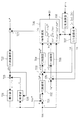
- FIG. 2 is a circuit diagram showing a conventional configuration that can be employed as the converter waveform controller 7 of FIG. In this configuration, the switching control signal G0 is output as the switching control signal Gcnv. Further, this configuration corresponds to a configuration obtained by simplifying the contents disclosed in Patent Document 2.
- the phase calculation unit 708 determines the power supply phase ⁇ based on the zero-cross signal ⁇ rs of the RS phase voltage, and supplies this to the phase conversion unit 707 and the PWM control unit 709.
- the phase conversion unit 707 performs three-phase / two-phase conversion to the d-axis-q-axis coordinate system, which is the rotational coordinate system, according to the power supply phase ⁇ , and d which is the d-axis component of the line currents Ir, Is, It.
- An axial current Id and a q-axis current Iq that is a q-axis component are calculated.
- the d-axis current Id and the q-axis current Iq contribute to active power and reactive power, respectively. Therefore, it is desirable that the q-axis current Iq is small in order to improve the power factor.
- the line current It is determined from the line currents Ir and Is. Therefore, the input of the line current It to the phase conversion unit 707 may be omitted, and this omission is indicated by enclosing the symbol It in parentheses in FIG.
- the adder / subtractor 701 obtains a voltage deviation ⁇ Vdc by subtracting the DC voltage Vdc from the DC voltage command value Vdc * .
- the PI control unit 702 obtains the d-axis current command value Id * by performing PI control based on the voltage deviation ⁇ Vdc.
- the d-axis current command value Id * corresponds to the command value of the d-axis current Id.
- the adder / subtractor 703 obtains a current deviation ⁇ Id by subtracting the d-axis current Id from the d-axis current command value Id * .
- the PI control unit 704 obtains a d-axis voltage command value Vd * by performing PI control based on the current deviation ⁇ Id.
- the d-axis voltage command value Vd * corresponds to the command value of the d-axis voltage Vd.
- the adder / subtractor 705 subtracts the q-axis current Iq from the q-axis current command value Iq * to obtain a current deviation ⁇ Id.
- the q-axis current command value Iq * corresponds to the command value of the q-axis current Id.
- the PI control unit 706 obtains a q-axis voltage command value Vq * by performing PI control based on the current deviation ⁇ Iq.
- the q-axis voltage command value Vq * corresponds to the command value of the q-axis voltage Vq.
- the PWM control unit 709 receives the d-axis voltage command value Vd *, the q-axis voltage command value Vq * , and the power supply phase ⁇ , and generates a switching control signal G0 based on these.
- the switching control signal G0 is used as the switching control signal Gcnv shown in FIG. Since the generation of the switching control signal G0 is performed using a known technique, a detailed description thereof is omitted.
- the voltage Vi is estimated here by ⁇ (Vd * 2 + Vq * 2 ).
- the DC voltage Vdc is also given to the PWM control unit 709, and the modulation factor Ks is obtained by ⁇ 2 (Vi / Vdc).
- voltage Vi is an effective value per phase of the voltage input to converter 3, and thus modulation factor Ks is the ratio of the peak value of input voltage Vi to DC voltage Vdc.
- the adder / subtractor 721 subtracts the command value Ks * from the modulation rate Ks, and the difference is proportionally calculated in the proportional calculation unit 722 to obtain the modulation rate deviation ⁇ K.
- the multiplier 723 multiplies the deviation ⁇ K by a coefficient ⁇ that takes a binary value of 0 or 1.
- the integrator 724 integrates the multiplication result ⁇ ⁇ ⁇ K to generate a DC voltage command value Vdc * .
- Limiting unit 725 receives DC voltage command value Vdc * and outputs a value of 1 as coefficient ⁇ when it is within a desired range.
- the value 0 is adopted as the coefficient ⁇ if the deviation ⁇ K is negative
- the value 1 is adopted as the coefficient ⁇ if the deviation ⁇ K is positive.
- value 1 is adopted as coefficient ⁇ if deviation ⁇ K is negative
- value 0 is adopted as coefficient ⁇ if deviation ⁇ K is positive.
- FIG. 3 is a graph showing the operation of each part of the configuration shown in FIG. 2 when the power supply voltage instantaneously drops from 400 V to 340 V and then returns.
- the time when the instantaneous voltage drop occurs and the time when the voltage drops are indicated by times t0 and t1, respectively.
- the graph shows values ⁇ Id * and ⁇ Id obtained by changing the signs of the d-axis current command value Id * and the d-axis current Id. Is shown.
- Variation of such d-axis current Id leads the steep drop of the d-axis voltage command value Vd outputted from the PI control unit 704 * (the graph of FIG. 3 fourth stage). Since the calculation in the PI control unit 704 has an integral term, the value s2 due to the integral term is gently reduced. However, since the influence of the integral term in the PI control unit 704 is usually small and the influence of the proportional term is large, the d-axis voltage command value Vd * is greatly affected by the fluctuation of the d-axis current Id as described above.
- a steep drop in the d-axis voltage command value Vd * causes a steep drop in the voltage Vi. Since the drop in the DC voltage Vdc is slower than this, the modulation factor Ks drops sharply (the first graph in FIG. 3). ). Thereafter, the DC voltage Vdc also decreases (the second graph in FIG. 3), and the modulation factor Ks increases (the first graph in FIG. 3).
- the deviation ⁇ K becomes negative, and the DC voltage command value Vdc * gradually decreases due to the function of the integration unit 724.
- the DC voltage command value Vdc * is slower than the DC voltage Vdc, so the deviation ⁇ Vdc swings positively, and the d-axis current command value Id * decreases (value ⁇ Id * increases).
- the DC voltage command value Vdc * also decreases thereafter, the deviation ⁇ Vdc becomes small (see the second stage in FIG. 3).
- the d-axis current command value Id * output from the PI control unit 702 increases rapidly (value ⁇ Id * decreases), and the current deviation ⁇ Id becomes positive. Therefore, the d-axis voltage command value Vd * output from the PI control unit 704 increases. As described above, since the influence of the integral term in the PI control unit 704 is small and the influence of the proportional term is large, the d-axis voltage command value Vd * increases rapidly.
- converter 3 operates as a step-down converter for DC voltage Vdc, it operates in a rectifier mode and modulation factor Ks takes a maximum value of 1. As a result, the deviation ⁇ K becomes positive.
- the DC voltage command value Vdc * rises slowly by the integration calculation in the integration unit 724, and eventually coincides with the DC voltage Vdc at time t2.
- the value s1 due to the integral term gradually decreases due to the integration operation of the deviation ⁇ Vdc ( ⁇ 0) in the PI control unit 702.
- the DC voltage command value Vdc * continues to increase after time t2
- the deviation ⁇ Vdc becomes positive after time t2, and the value s1 increases gently.
- the d-axis current command value Id * slowly decreases (value ⁇ Id * increases), and coincides with the d-axis current Id at time t3. That is, the value s2 by the integral term of the PI control unit 704 continues to increase gently until time t3, and then decreases. However, since the influence of the integral term of the PI control unit 704 is small as described above, the timing when the d-axis voltage command value Vd * takes the maximum value is earlier than the time t3 when the value s2 takes the maximum value.
- FIG. 4 is a circuit diagram showing a configuration of the converter waveform control unit according to the first embodiment that can be employed as the converter waveform control unit 7 of FIG. In this configuration, the switching control signal G1 is output as the switching control signal Gcnv.
- the adder / subtracters 701, 703, 705, PI controllers 702, 704, 706, phase converter 707, phase calculator 708, and PWM controller 709 employed in the converter waveform controller according to the present embodiment are shown in FIG. The one shown is adopted.
- a voltage command value calculation unit 710 is employed instead of the adder / subtractor 721, the proportional calculation unit 722, the multiplication unit 723, the integrator 724, and the limiting unit 725 shown in FIG.
- the voltage command value calculation unit 710 generates a DC voltage command value Vdc * based on the d-axis voltage command value Vd * output from the PI control unit 704, and gives this to the adder / subtractor 701.
- the generation of the DC voltage command value Vdc * is based on the d-axis voltage command value Vd * and requires a power supply phase, but does not require the voltage of the multiphase power supply itself. Therefore, a circuit configuration for detecting the voltage of the multiphase power supply is not required, and the DC voltage Vdc is controlled and the power factor of input power is easily improved while suppressing the size and manufacturing cost.
- the value (Vd * ⁇ r ⁇ Id) is an estimated value of the power supply voltage in the steady state according to the definition of the d-axis, and the control of the DC voltage Vdc based on the power supply voltage can be performed substantially without actually measuring the power supply voltage. This is because it can be realized.
- the value of the resistance component r is preferably stored in the voltage command value calculation unit 710 or input from the outside.
- the d-axis current Id can be obtained from the phase conversion unit 707.
- Vd Vs + (Ls + r) Id ⁇ L ⁇ Iq
- the value (Vd * ⁇ r ⁇ Id) is estimated by using the d-axis voltage command value Vd * instead of the d-axis voltage Vd . Treat as a value.
- the DC voltage command value Vdc * may be determined based on a value (Vi ⁇ r ⁇ Id) obtained by subtracting at least the product r ⁇ Id from the input voltage Vi (or its estimated value) to the converter 3. .
- a value (Vi ⁇ r ⁇ Id) obtained by subtracting at least the product r ⁇ Id from the input voltage Vi (or its estimated value) to the converter 3. .
- the phase difference ⁇ is small, the power supply voltage Vs becomes almost equal to the voltage Vi. Therefore, such a determination can be made.
- FIG. 5 is a graph showing the operation of each part of the configuration shown in FIG. 4 when the power supply voltage instantaneously drops from 400 V to 340 V and then returns. Similarly to FIG. 3, the time when the instantaneous voltage drop occurs and the time when the voltage drops are indicated by time t0 and t1, respectively.
- FIG. 6 is a circuit diagram showing a configuration according to a second embodiment that can be adopted as the converter waveform control unit 7 of FIG. In this configuration, the switching control signal G2 is output as the switching control signal Gcnv.
- voltage controllers 711 and 713 and adders 712 and 714 are added to the configuration employed in the first embodiment.
- the voltage control unit 711 outputs the product ⁇ Ld ⁇ Id * of the d-axis current command value Id * , the d-axis inductance Ld of the reactor group 2, and the angular frequency ⁇ of the power supply voltage to the adder 712.
- the voltage control unit 713 outputs the product ⁇ Lq ⁇ Iq * of the q-axis current command value Iq * , the q-axis inductance Lq of the reactor group 2 and the angular frequency ⁇ to the adder 714.
- Each of the d-axis inductance Ld and the q-axis inductance Lq is obtained by converting the inductance of the reactor group 2 into the d-axis-q-axis coordinate system. However, the values of the reactors constituting the reactor group 2 are assumed to be equal to each other.
- the value of the power supply frequency f is preferably stored in the voltage command value calculation unit 710 or input from the outside (calculated from the zero cross signal ⁇ rs).
- the input of the angular frequency ⁇ to the voltage control units 711 and 713 is omitted in order to avoid complication of the drawing.
- the adder 712 adds the product ⁇ Ld ⁇ Id * to the output of the PI control unit 704 to generate a d-axis voltage command value Vd * .
- the adder 714 adds the product ⁇ Lq ⁇ Iq * to the output of the PI control unit 706 to generate a q-axis voltage command value Vq * .
- the voltage control units 711 and 713 and the adders 712 and 714 have a function of compensating for an interference term caused by the reactor group 2. Since the compensation of the interference term itself is a well-known technique, a detailed description thereof is omitted.
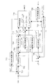
- FIG. 7 is a circuit diagram showing a configuration according to a third embodiment that can be adopted as the converter waveform control section 7 of FIG. In this configuration, the switching control signal G3 is output as the switching control signal Gcnv.
- the configuration adopted in the third embodiment is different from the configuration adopted in the second embodiment in that the DC voltage command value Vdc * is changed to the d-axis voltage command value Vd * in the voltage command value calculation unit 710 .
- the difference is that the estimated value estimated by the PWM control unit 709 as ⁇ (Vd * 2 + Vq * 2 ) is adopted here by the PWM control unit 709.
- the voltage control units 711 and 713 and the adders 712 and 714 may be omitted in the present embodiment as in the first embodiment.
- the estimation of the voltage Vi may be obtained by Vs / cos ⁇ .
- Vdc * Operation of voltage command value calculation unit 710. Specifically, the DC voltage command value Vdc * can be set as follows.
- the product of the estimated value Vi of the multiphase voltage input to the converter 3 as the DC voltage command value Vdc * and the constant ⁇ 2 ⁇ K1 is employed.
- the constant K1 corresponds to the modulation factor Ks, and the modulation factor Ks can be kept constant even if the power supply voltage varies.
- FIG. 8 is a block diagram illustrating the configuration of the voltage command value calculation unit 710
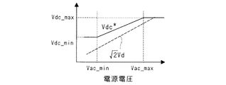
- FIG. 9 is a graph showing the relationship between the DC voltage command value Vdc * and the power supply voltage.
- the proportional calculation unit 710a receives the d-axis voltage command value Vd * and gives the product of this and the constant ⁇ 2 ⁇ K1 to the limiter 710b.
- the limiter 710b slices the above product with the lower limit value Vdc_min and the upper limit value Vdc_max, and outputs it as a DC voltage command value Vdc * .
- the step-up rate can be kept constant in the range of power supply voltage (Vac_min to Vac_max) in which DC voltage command value Vdc * can take a value between lower limit value Vdc_min and upper limit value Vdc_max.
- (C-2) Linear calculation.
- a value obtained by adding a constant V1 to the product of the d-axis voltage command value Vd * and ⁇ 2 ( ⁇ 2 ⁇ Vd * + V1) is adopted as the DC voltage command value Vdc * .
- a value ( ⁇ 2 ⁇ Vi + V1) obtained by adding a constant V1 to the product of the estimated value Vi and ⁇ 2 of the multiphase voltage input to the converter 3 as the DC voltage command value Vdc * is adopted.
- the constant V1 gives a constant boost to the DC voltage command value Vdc * . Therefore, the fluctuation range of the DC voltage command value Vdc * when the power supply voltage fluctuates can be suppressed as compared with the case where the proportional calculation shown in (c-1) is adopted.
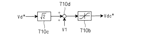
- FIG. 10 is a block diagram illustrating the configuration of the voltage command value calculation unit 710
- FIG. 11 is a graph showing the relationship between the DC voltage command value Vdc * and the power supply voltage.
- the proportional calculation unit 710c receives the d-axis voltage command value Vd * , multiplies it by ⁇ 2, and gives it to the adder 710d.
- the adder 710d adds the constant V1 to ⁇ square root over (2) ⁇ Vd * and supplies the result to the limiter 710b.
- the limiter 710b slices the value ( ⁇ 2 ⁇ Vd * + V1) with the lower limit value Vdc_min and the upper limit value Vdc_max, and outputs the result as a DC voltage command value Vdc * . 10 and 11, the d-axis voltage command value Vd * can be read as the estimated value Vi of the multiphase voltage input to the converter 3.
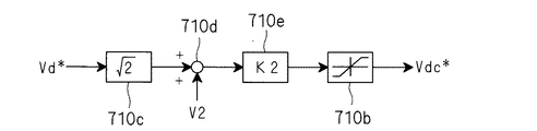
- a value obtained by multiplying the product of the estimated value Vi of the multiphase voltage Vi and ⁇ 2 input to the converter 3 by the constant V2 ( ⁇ 2 ⁇ Vi + V2) as the DC voltage command value Vdc * by K2 is adopted.
- FIG. 12 is a block diagram illustrating the configuration of the voltage command value calculation unit 710
- FIG. 13 is a graph showing the relationship between the DC voltage command value Vdc * and the power supply voltage.
- the proportional calculation unit 710c receives the d-axis voltage command value Vd * , multiplies it by ⁇ 2, and gives it to the adder 710d.
- the adder 710d adds the constant V2 to the value ⁇ 2 ⁇ Vd * and supplies the result to the multiplier 710e.
- the multiplier 710e gives the value ( ⁇ 2 ⁇ Vd * + V2) ⁇ K2 to the limiter 710b.
- the limiter 710b slices the value ( ⁇ 2 ⁇ Vd * + V2) ⁇ K2 with the lower limit value Vdc_min and the upper limit value Vdc_max, and outputs it as a DC voltage command value Vdc * . 12 and 13, the d-axis voltage command value Vd * can be read as the estimated value Vi of the multiphase voltage input to the converter 3.
- FIG. 14 is a block diagram illustrating the configuration of the voltage command value calculation unit 710.
- the average value calculation unit 710f calculates an average value of the d-axis voltage command value Vd * over a predetermined period.
- the proportional calculation unit 710f multiplies the average value by a constant K3 and outputs a DC voltage command value Vdc * .
- FIG. 15 is a block diagram illustrating another configuration of the voltage command value calculation unit 710.
- the proportional calculation unit 710h obtains the product of the d-axis voltage command value Vd * and the constant K4.
- the first-order lag calculation unit 710i performs first-order lag calculation on the product.
- Both of the above-described two configurations perform filtering on the d-axis voltage command value Vd * , and can remove high-frequency fluctuation components of the DC voltage command value Vdc * .
- the response of the voltage command value calculation unit 710 that determines the DC voltage command value Vdc * is a response for obtaining the d-axis voltage command value Vd * based on the deviation ⁇ Vdc (specifically, the response of the PI control units 702 and 704), By sufficiently delaying the response (specifically, the response of the PI control unit 706) for obtaining the q-axis voltage command value Vq * , a stable control system with respect to the transient response is configured.
- the d-axis voltage command value Vd * may be replaced with the estimated value Vi of the multiphase voltage input to the converter 3.
- the calculation of the DC voltage command value Vd * may be changed in accordance with the command value J from the inverter control unit 8 (see FIG. 1). Specifically, for example, when the three-phase load 6 is a motor and it is necessary to rotate the motor 6 at a high speed, the inverter 4 is driven in response to the necessity. When such driving is performed, the inverter control unit 8 causes the inverter 4 to drive the motor for high speed rotation, for example, to advance the current phase and perform field weakening control. When causing the inverter 4 to perform such high-speed rotation driving, the inverter control unit 8 outputs the command value J, thereby controlling the operation of the converter waveform control unit 7.
- the operation of the converter waveform control unit 7, that is, the operation of the converter 3 is linked with the operation of the inverter control unit 8, and thus the operation of the inverter 4, so that only when high-speed rotation of the motor is necessary,
- the DC voltage Vdc can be set high.
- high-efficiency control that normally suppresses boosting of the DC voltage Vdc is performed, and high-speed rotation can be realized only when necessary, thereby expanding the inverter operating range.
Landscapes
- Engineering & Computer Science (AREA)
- Power Engineering (AREA)
- Inverter Devices (AREA)
- Rectifiers (AREA)
- Dc-Dc Converters (AREA)
- Control Of Ac Motors In General (AREA)
- Control Of Motors That Do Not Use Commutators (AREA)
Abstract
Priority Applications (5)
| Application Number | Priority Date | Filing Date | Title |
|---|---|---|---|
| CN2009801132946A CN102007678B (zh) | 2008-04-18 | 2009-03-16 | 变流器控制方法 |
| KR1020107022893A KR101193301B1 (ko) | 2008-04-18 | 2009-03-16 | 컨버터의 제어 방법 |
| EP09731707.7A EP2273661B1 (fr) | 2008-04-18 | 2009-03-16 | Procédé de commande de convertisseur |
| US12/988,177 US20110038192A1 (en) | 2008-04-18 | 2009-03-16 | Converter control method |
| AU2009237116A AU2009237116B2 (en) | 2008-04-18 | 2009-03-16 | Converter control method |
Applications Claiming Priority (2)
| Application Number | Priority Date | Filing Date | Title |
|---|---|---|---|
| JP2008108897A JP5365058B2 (ja) | 2008-04-18 | 2008-04-18 | コンバータの制御方法 |
| JP2008-108897 | 2008-04-18 |
Publications (1)
| Publication Number | Publication Date |
|---|---|
| WO2009128312A1 true WO2009128312A1 (fr) | 2009-10-22 |
Family
ID=41199012
Family Applications (1)
| Application Number | Title | Priority Date | Filing Date |
|---|---|---|---|
| PCT/JP2009/055014 WO2009128312A1 (fr) | 2008-04-18 | 2009-03-16 | Procédé de commande de convertisseur |
Country Status (7)
| Country | Link |
|---|---|
| US (1) | US20110038192A1 (fr) |
| EP (1) | EP2273661B1 (fr) |
| JP (1) | JP5365058B2 (fr) |
| KR (1) | KR101193301B1 (fr) |
| CN (1) | CN102007678B (fr) |
| AU (1) | AU2009237116B2 (fr) |
| WO (1) | WO2009128312A1 (fr) |
Cited By (1)
| Publication number | Priority date | Publication date | Assignee | Title |
|---|---|---|---|---|
| CN102372201A (zh) * | 2010-08-26 | 2012-03-14 | 上海三菱电梯有限公司 | 电梯贮能装置 |
Families Citing this family (11)
| Publication number | Priority date | Publication date | Assignee | Title |
|---|---|---|---|---|
| JP5567365B2 (ja) * | 2010-03-10 | 2014-08-06 | 株式会社ダイヘン | インバータ制御回路、および、このインバータ制御回路を備えた系統連系インバータシステム |
| EP2654199B1 (fr) * | 2012-04-18 | 2017-08-02 | Siemens Aktiengesellschaft | Procédé et dispositif de stabilisation d'une tension électrique au moyen d'une régulation orientée champ |
| KR101928435B1 (ko) | 2012-06-19 | 2018-12-12 | 삼성전자주식회사 | 전력 변환 장치 및 이의 제어 방법 |
| JP5712987B2 (ja) * | 2012-09-27 | 2015-05-07 | ダイキン工業株式会社 | 電力変換装置の制御方法 |
| US9331614B2 (en) * | 2013-02-08 | 2016-05-03 | Regal Beloit America, Inc. | Systems and methods for controlling electric machines |
| JP5742980B1 (ja) * | 2014-02-19 | 2015-07-01 | ダイキン工業株式会社 | 電力変換装置の制御方法 |
| CN104065276B (zh) * | 2014-06-27 | 2017-01-25 | 华为技术有限公司 | 一种三相不间断电源的控制方法、装置和三相不间断电源 |
| ITUA20162878A1 (it) * | 2016-04-26 | 2017-10-26 | Phase Motion Control S P A | Dispositivo di alimentazione e azionamento per un motore elettrico a magneti permanenti |
| JP7154019B2 (ja) * | 2018-03-08 | 2022-10-17 | ナブテスコ株式会社 | Ac-ac電力変換装置 |
| JP2019193482A (ja) * | 2018-04-26 | 2019-10-31 | 三菱重工サーマルシステムズ株式会社 | 制御装置、空気調和機、制御方法及びプログラム |
| CN111371364B (zh) * | 2020-03-17 | 2022-03-25 | 美的集团股份有限公司 | 升降压驱动方法、装置、空调器和计算机可读存储介质 |
Citations (4)
| Publication number | Priority date | Publication date | Assignee | Title |
|---|---|---|---|---|
| JPH07245957A (ja) | 1994-03-04 | 1995-09-19 | Toshiba Corp | Pwmコンバータ装置 |
| JP2006006046A (ja) * | 2004-06-18 | 2006-01-05 | Daikin Ind Ltd | コンバータ制御方法及びコンバータ制御装置並びに空調機及びその制御方法及び制御装置 |
| JP2006006406A (ja) | 2004-06-22 | 2006-01-12 | Toshiba Tec Corp | 電気掃除機用フィルタおよび電気掃除機 |
| JP2006115609A (ja) * | 2004-10-14 | 2006-04-27 | Daikin Ind Ltd | コンバータの制御方法及びコンバータの制御装置 |
Family Cites Families (19)
| Publication number | Priority date | Publication date | Assignee | Title |
|---|---|---|---|---|
| JPH0734629B2 (ja) * | 1987-06-05 | 1995-04-12 | 三菱電機株式会社 | 電力変換器 |
| JP2833187B2 (ja) * | 1990-01-17 | 1998-12-09 | 富士電機株式会社 | 電力変換器の電流制御回路 |
| JPH05252748A (ja) * | 1992-03-05 | 1993-09-28 | Mitsubishi Electric Corp | Pwmコンバータ装置 |
| TW312759B (fr) * | 1995-09-27 | 1997-08-11 | Mitsubishi Electric Corp | |
| KR0155940B1 (ko) * | 1995-12-29 | 1998-12-15 | 김광호 | 부하전류 관측자를 이용한 정류기의 직류링크 전압제어 장치 및 펄스폭변조 정류기의 전향제어 장치 |
| JPH1127946A (ja) * | 1997-07-08 | 1999-01-29 | Fuji Electric Co Ltd | パルス幅変調制御コンバータ |
| DE19844050A1 (de) * | 1998-09-25 | 2000-03-30 | Abb Daimler Benz Transp | Verfahren zum Steuern und Regeln eines elektrischen Antriebes sowie Vorrichtung zur Durchführung des Verfahrens |
| JP2000134956A (ja) * | 1998-10-28 | 2000-05-12 | Mitsubishi Electric Corp | 交直電力変換装置 |
| US6130832A (en) * | 1999-11-08 | 2000-10-10 | Otis Elevator Company | Active filtering of AC/DC switched converter input current |
| JP3650565B2 (ja) * | 2000-04-03 | 2005-05-18 | 東芝三菱電機産業システム株式会社 | 電力変換装置 |
| KR20050003732A (ko) * | 2003-07-04 | 2005-01-12 | 현대자동차주식회사 | 유도 전동기용 벡터 제어형 듀얼 인버터 시스템 |
| JP4060777B2 (ja) * | 2003-09-03 | 2008-03-12 | 株式会社東芝 | 電気車制御装置 |
| JP4601044B2 (ja) * | 2004-08-30 | 2010-12-22 | 日立アプライアンス株式会社 | 電力変換装置およびその電力変換装置を備えた空気調和機 |
| KR100645807B1 (ko) * | 2004-12-06 | 2007-02-28 | 엘지전자 주식회사 | 모터 기동 제어장치 및 그 방법 |
| JP4634193B2 (ja) * | 2005-03-14 | 2011-02-16 | 日立オートモティブシステムズ株式会社 | 同期電動機 |
| JP2007006601A (ja) * | 2005-06-23 | 2007-01-11 | Toshiba Corp | 電力変換装置 |
| JP3927584B2 (ja) * | 2005-10-26 | 2007-06-13 | 三菱電機株式会社 | 自動車用動力制御装置 |
| US7511385B2 (en) * | 2005-11-11 | 2009-03-31 | Converteam Ltd | Power converters |
| JP4634321B2 (ja) * | 2006-02-28 | 2011-02-16 | 日立オートモティブシステムズ株式会社 | 電動4輪駆動車用制御装置 |
-
2008
- 2008-04-18 JP JP2008108897A patent/JP5365058B2/ja active Active
-
2009
- 2009-03-16 EP EP09731707.7A patent/EP2273661B1/fr active Active
- 2009-03-16 KR KR1020107022893A patent/KR101193301B1/ko active IP Right Grant
- 2009-03-16 AU AU2009237116A patent/AU2009237116B2/en active Active
- 2009-03-16 CN CN2009801132946A patent/CN102007678B/zh active Active
- 2009-03-16 US US12/988,177 patent/US20110038192A1/en not_active Abandoned
- 2009-03-16 WO PCT/JP2009/055014 patent/WO2009128312A1/fr active Application Filing
Patent Citations (4)
| Publication number | Priority date | Publication date | Assignee | Title |
|---|---|---|---|---|
| JPH07245957A (ja) | 1994-03-04 | 1995-09-19 | Toshiba Corp | Pwmコンバータ装置 |
| JP2006006046A (ja) * | 2004-06-18 | 2006-01-05 | Daikin Ind Ltd | コンバータ制御方法及びコンバータ制御装置並びに空調機及びその制御方法及び制御装置 |
| JP2006006406A (ja) | 2004-06-22 | 2006-01-12 | Toshiba Tec Corp | 電気掃除機用フィルタおよび電気掃除機 |
| JP2006115609A (ja) * | 2004-10-14 | 2006-04-27 | Daikin Ind Ltd | コンバータの制御方法及びコンバータの制御装置 |
Cited By (1)
| Publication number | Priority date | Publication date | Assignee | Title |
|---|---|---|---|---|
| CN102372201A (zh) * | 2010-08-26 | 2012-03-14 | 上海三菱电梯有限公司 | 电梯贮能装置 |
Also Published As
| Publication number | Publication date |
|---|---|
| US20110038192A1 (en) | 2011-02-17 |
| EP2273661B1 (fr) | 2019-11-20 |
| CN102007678A (zh) | 2011-04-06 |
| EP2273661A4 (fr) | 2017-02-22 |
| KR101193301B1 (ko) | 2012-10-19 |
| AU2009237116A1 (en) | 2009-10-22 |
| CN102007678B (zh) | 2013-04-10 |
| JP5365058B2 (ja) | 2013-12-11 |
| EP2273661A1 (fr) | 2011-01-12 |
| AU2009237116B2 (en) | 2013-01-10 |
| JP2009261169A (ja) | 2009-11-05 |
| KR20100124816A (ko) | 2010-11-29 |
Similar Documents
| Publication | Publication Date | Title |
|---|---|---|
| WO2009128312A1 (fr) | Procédé de commande de convertisseur | |
| US9257931B2 (en) | Power conversion apparatus | |
| JP5542609B2 (ja) | 無効電力補償装置 | |
| JP5097453B2 (ja) | 電力変換装置 | |
| JP5742980B1 (ja) | 電力変換装置の制御方法 | |
| EP3125420B1 (fr) | Dispositif de conversion d'énergie | |
| WO2014050441A1 (fr) | Procédé de commande d'appareil de conversion de puissance | |
| EP2763301B1 (fr) | Procédé de commande de convertisseur de puissance | |
| JP2008141887A (ja) | 瞬時電圧低下補償回路、電力変換装置、瞬時電圧低下補償方法及び瞬時電圧低下補償プログラム | |
| JP2004320985A (ja) | モータ駆動用インバータ制御装置および空気調和機 | |
| JP6237852B1 (ja) | アクティブフィルタの制御装置 | |
| US11218107B2 (en) | Control device for power converter | |
| JP6079094B2 (ja) | インバータ制御装置 | |
| JP4909857B2 (ja) | コンバータ装置 | |
| JP4893219B2 (ja) | 電力変換装置 | |
| JP4649940B2 (ja) | コンバータの制御方法及びコンバータの制御装置 | |
| JP5928216B2 (ja) | インバータ制御装置 | |
| JPH10127056A (ja) | パルス幅変調コンバータ装置 | |
| WO2024033958A1 (fr) | Dispositif de conversion d'énergie | |
| JP6340970B2 (ja) | 制御装置 | |
| JP6146511B2 (ja) | インバータ制御装置 | |
| JP6729249B2 (ja) | 電力変換器の制御装置 |
Legal Events
| Date | Code | Title | Description |
|---|---|---|---|
| WWE | Wipo information: entry into national phase |
Ref document number: 200980113294.6 Country of ref document: CN |
|
| 121 | Ep: the epo has been informed by wipo that ep was designated in this application |
Ref document number: 09731707 Country of ref document: EP Kind code of ref document: A1 |
|
| ENP | Entry into the national phase |
Ref document number: 20107022893 Country of ref document: KR Kind code of ref document: A |
|
| WWE | Wipo information: entry into national phase |
Ref document number: 2009237116 Country of ref document: AU Ref document number: 12988177 Country of ref document: US |
|
| WWE | Wipo information: entry into national phase |
Ref document number: 2009731707 Country of ref document: EP |
|
| NENP | Non-entry into the national phase |
Ref country code: DE |
|
| ENP | Entry into the national phase |
Ref document number: 2009237116 Country of ref document: AU Date of ref document: 20090316 Kind code of ref document: A |