WO2009122656A1 - パイプラインa/d変換器 - Google Patents
パイプラインa/d変換器 Download PDFInfo
- Publication number
- WO2009122656A1 WO2009122656A1 PCT/JP2009/000959 JP2009000959W WO2009122656A1 WO 2009122656 A1 WO2009122656 A1 WO 2009122656A1 JP 2009000959 W JP2009000959 W JP 2009000959W WO 2009122656 A1 WO2009122656 A1 WO 2009122656A1
- Authority
- WO
- WIPO (PCT)
- Prior art keywords
- signal
- input
- unit
- test
- conversion
- Prior art date
- Legal status (The legal status is an assumption and is not a legal conclusion. Google has not performed a legal analysis and makes no representation as to the accuracy of the status listed.)
- Ceased
Links
Images


Classifications
-
- H—ELECTRICITY
- H03—ELECTRONIC CIRCUITRY
- H03M—CODING; DECODING; CODE CONVERSION IN GENERAL
- H03M1/00—Analogue/digital conversion; Digital/analogue conversion
- H03M1/10—Calibration or testing
- H03M1/1071—Measuring or testing
- H03M1/108—Converters having special provisions for facilitating access for testing purposes
-
- H—ELECTRICITY
- H03—ELECTRONIC CIRCUITRY
- H03M—CODING; DECODING; CODE CONVERSION IN GENERAL
- H03M1/00—Analogue/digital conversion; Digital/analogue conversion
- H03M1/12—Analogue/digital converters
- H03M1/14—Conversion in steps with each step involving the same or a different conversion means and delivering more than one bit
- H03M1/16—Conversion in steps with each step involving the same or a different conversion means and delivering more than one bit with scale factor modification, i.e. by changing the amplification between the steps
- H03M1/164—Conversion in steps with each step involving the same or a different conversion means and delivering more than one bit with scale factor modification, i.e. by changing the amplification between the steps the steps being performed sequentially in series-connected stages
- H03M1/167—Conversion in steps with each step involving the same or a different conversion means and delivering more than one bit with scale factor modification, i.e. by changing the amplification between the steps the steps being performed sequentially in series-connected stages all stages comprising simultaneous converters
-
- H—ELECTRICITY
- H03—ELECTRONIC CIRCUITRY
- H03M—CODING; DECODING; CODE CONVERSION IN GENERAL
- H03M1/00—Analogue/digital conversion; Digital/analogue conversion
- H03M1/12—Analogue/digital converters
- H03M1/34—Analogue value compared with reference values
- H03M1/38—Analogue value compared with reference values sequentially only, e.g. successive approximation type
- H03M1/44—Sequential comparisons in series-connected stages with change in value of analogue signal
Definitions
- the present invention relates to a pipelined A / D converter, and more particularly to a technique for correcting its output.
- Pipeline AD converters are widely used in recent years as circuits excellent in high speed and power consumption. However, with the advancement of the performance of equipment, pipeline AD converters are required to have higher precision as well as high speed, low voltage, many bits, and low cost.
- FIG. 16 is a block diagram showing a basic configuration of a pipelined A / D converter.
- This pipeline A / D converter includes n stages of cascade-connected stages, ie, the first stage 1 [1] to the nth stage 1 [n] and the flash AD converter 2 of the final stage.
- the input analog signal Vin is converted into a digital signal by one bit from the upper bit to the lower bit by n stages of stages.
- the digital operation unit 6 By combining the n stages of stages and the output digital signal of the flash AD converter 2 by the digital operation unit 6, an output signal obtained by A / D converting the input analog signal Vin with a desired number of bits is obtained.
- each stage is configured of an AD conversion unit 3, a DA conversion unit 4, and a remainder calculation unit 5.
- the AD conversion unit 3 generates and outputs a digital signal in which the input analog signal to this stage is binarized, and also supplies it to the DA conversion unit 4.
- the DA converter 4 generates an analog reference signal based on the digital signal output from the AD converter 3, and supplies the analog reference signal to the remainder calculator 5.
- the remainder operation unit 5 subtracts the analog reference signal output from the DA conversion unit 4 from the input analog signal to the current stage to perform amplification to generate a remainder analog signal and input it to the next stage. Supply as an analog signal.
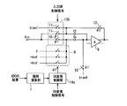
- FIG. 17 shows a circuit for obtaining a predetermined function by the DA converter 4 and the remainder calculator 5.
- the DA conversion unit 4 includes a logic operation unit 7 and a voltage supply unit 8.
- Other elements, that is, the operational amplifier 9, the sampling capacitance Cs, the feedback loop capacitance Cf, and the switches 10 to 12 constitute a remainder operation unit 5 in FIG.
- the analog reference signal output from the DA converter 4 is supplied to the connection node between the sampling capacitor Cs and the switch 10. Further, the operational amplifier 9 side of the sampling capacitance Cs is connected to the bias 0 via the switch 15.
- the capacitance values of the sampling capacitance Cs and the feedback loop capacitance Cf are represented by Cs and Cf, respectively.
- the voltage supply unit 8 selectively supplies three reference voltages + Vref, 0 V, and -Vref by switching three switches.
- the logic operation unit 7 outputs a signal for switching the switch of the voltage supply unit 8 based on the value of the digital signal output from the AD conversion unit 3. Thereby, in the voltage supply unit 8, one of the three reference voltages is selected according to the value of the digital signal, and is supplied as the analog reference signal Vdac.
- This circuit performs operations of a sampling period and an amplification period by the clock ⁇ ⁇ ⁇ ⁇ 1 and the clock 22 shown in FIG. 17 alternately taking high level (H) and low level (L) values.
- the clock 11 is H and the clock 22 is L
- the switches 10 and 11 are on and the switch 12 is off
- the input analog signal Vin is sampled by the sampling capacitor Cs.
- the clock 11 is L and the clock 22 is H
- the switches 10 and 11 are off and the switch 12 is on, and the charge sampled by the sampling capacitor Cs is redistributed to the sampling capacitor Cs and the feedback loop capacitor Cf.
- the logic operation unit 7 operates and the voltage supply unit 8 supplies the analog reference signal Vdac to the sampling capacitor Cs.
- the output signal Vout amplified by the operational amplifier 9 is as follows.
- the output signal Vout of the operational amplifier 9 will be described with reference to the input / output characteristics of FIG.
- the horizontal axis in FIG. 18 indicates the input analog signal Vin for each stage.
- the vertical axis represents the output signal Vout of the operational amplifier 9.
- the level of the input analog signal Vin on the horizontal axis is the first region (-Vref to -Vref / 4), the second region (-Vref / 4 to + Vref / 4), and the third region (-Vref). Divided into + Vref / 4 to + Vref).
- the AD converter 3 generates a ternary digital signal from the input analog signal Vin using a reference voltage corresponding to the boundary of each area.
- the voltage supply unit 8 selects one of the voltages + Vref, 0 V, and -Vref according to the control signal output from the logic operation unit 7 based on the digital signal. Further, as a result of the calculation of the equation (2), the input / output characteristics of the output signal Vout of the operational amplifier 9 with respect to the input analog signal Vin are as shown in FIG.
- the above-mentioned capacitance value error is a main cause of deterioration of the analog input / output characteristics of the stage, and eliminating this error leads to improvement of the conversion accuracy of the pipelined A / D converter.
- the allowable error is about 0.04% or less. It is extremely difficult to correct this error in the analog signal domain, and digital error correction is required.
- a pipeline A / D converter as shown in FIG. 19 is disclosed in Patent Document 1 as an example of a configuration for correcting a conversion error caused by such a capacitance value error.
- the A / D converter includes a plurality of stages 30 and variable stages 30A, a digital calculation unit 31, a control unit 32, a plurality of input switching units 33, a stage evaluation unit 34, a plurality of correction value calculation units 35, and an output correction unit Including 36.
- the stage 30 and the variable stage 30A each have the same function as the stages described above.
- the digital calculation unit 31 includes a digital calculation core 31a that adds the digital output of the corresponding stage to the digital output from the previous stage shifted by 1 bit corresponding to each stage.
- the control unit 32 controls the operation of the switch group in each input switching unit 33 and each variable stage 30A.
- the input switching unit 33 is provided corresponding to the variable stage 30A, and switches the input of the corresponding variable stage 30A between the normal input signal and the test signal under the control of the control unit 32.
- the normal input signal is an input analog signal to each stage in the normal conversion operation.
- the test signal is an analog signal of a predetermined magnitude for detecting a capacitance value error of the stage.
- the test signal is generated, for example, using a D / A converter or the like not shown.
- the stage evaluation unit 34 estimates an analog output error of each variable stage 30A based on the digital output of the output correction unit 36. That is, in a state where the test signal is input to the variable stage 30A (test stage) which is trying to estimate the capacitance value error, the digital output obtained from the pipeline A / D converter corresponds to the capacitance value error of the test stage. Conversion error is included. Therefore, an analog output error is estimated from this digital output.
- the correction value calculation unit 35 is provided corresponding to the variable stage 30A, and generates an output error characteristic of each variable stage 30A based on the capacitance value error estimated by the stage evaluation unit 34. Based on the characteristics, the correction value calculation unit 35 uses the intermediate output of the digital calculation unit 31 input via the delay element 37 to calculate the digital output error of the corresponding variable stage 30A as a digital correction value.
- the output correction unit 36 corrects the digital output of the digital calculation unit 31 based on the digital correction value output from each correction value calculation unit 35.
- the output error caused by the capacitance value error of the feedback loop capacitance and sampling capacitance in the variable stage 30A is estimated, and the digital correction value is calculated based on the estimation error. Then, the digital output of the pipelined A / D converter is corrected using these digital correction values.
- Patent Document 2 discloses a specific configuration for supplying a test signal as described above.
- test signal when the test signal is supplied via the test signal input line, a problem occurs in the accuracy of the supplied test signal. That is, since the line is different from a line for supplying a normal input analog signal, it is not in the same state as an actually input analog signal, and deterioration of the signal due to the length of a test signal input line and a parasitic element. Is also to occur. If the accuracy of the test signal is poor, high accuracy can not be expected for the evaluation result based on the test signal.
- the increase in circuit scale can not be avoided, and the evaluation result also depends on the characteristics of the test signal generation means.
- test signal supply to the stage is for correction of step errors, gain errors, offset errors of various AD converters, and other inspections and evaluations, in addition to correction of capacitance value errors as in the conventional example described above. It is also used when testing the test signal supply to the stage.
- the test signal supplied to the stage for various tests can be input by a small scale pipeline A / D without providing a test signal line separately from the line for normal operation. It is intended to provide a converter.
- a plurality of stages for performing A / D conversion corresponding to some bits are cascaded in a plurality of stages, and the analog signal input to the first stage is The upper stage to the lower stage are sequentially converted into digital signals through the following stages.
- the stages in each stage are configured to convert the analog signal in the stage to a digital signal corresponding to a part of bits and generate an AD converter, and the digital signal generated by the AD converter is multilevel.
- D / A converter which selects a predetermined reference voltage from the reference voltages of the above and outputs as an analog reference signal, adds / subtracts / subtracts the predetermined analog signal from the input analog signal and amplifies a predetermined multiple to generate a remainder analog signal.
- a remainder operation unit for supplying an input analog signal to the stages of the stages. For at least some of the stages, a test signal is input instead of the input analog signal to perform a predetermined test.
- the pipelined A / D converter tests the supply of the input analog signal to the remainder operation unit and the selection of the reference voltage of the DA conversion unit in the normal operation mode and
- the control unit includes a control unit that can be controlled according to each mode, and in the test mode, the control unit cuts off the supply of the input analog signal to the remainder operation unit, and the DA based on the digital signal.
- the selection of the reference voltage of the conversion unit is stopped, the selection of the reference voltage is performed based on the test DA conversion control signal, and the remainder operation unit receives the predetermined reference voltage in place of the input analog signal. Control to supply the test signal and the analog reference signal.
- the voltage supply unit is shared in the normal operation mode and the test mode to supply the test signal and the analog reference signal without providing the test signal line for the test signal supply. can do. Therefore, the test signal can be supplied with high accuracy. Further, since the voltage supply unit is shared, it is not necessary to provide a test signal generation unit such as a DA converter outside the A / D converter, and an increase in circuit scale can be suppressed.
- Block diagram showing a basic configuration of one stage constituting a pipeline A / D converter according to the first embodiment of the present invention Block diagram showing the specific configuration of the main part of the stage A block diagram showing a modification of the stage shown in FIG. 2
- Block diagram showing an essential part of one stage constituting a pipeline A / D converter in the second embodiment Block diagram showing the entire configuration of the stage Diagram showing analog input / output characteristics of the same stage Diagram showing an example of state transition in the sampling period and amplification period in the test mode of the same stage Diagram showing the state of the remainder operation unit in the normal operation mode and test mode of the same stage
- the pipeline A / D converter of the present invention can take the following aspects based on the above configuration.
- the remainder operation unit includes an input switch that controls the input of the input analog signal, and the DA conversion unit generates a voltage supply unit that selects and outputs the predetermined reference voltage, and the AD conversion unit generates And a logical operation unit for outputting a signal for controlling selection by the voltage supply unit based on the digital signal, the control unit selecting from an output signal of the logical operation unit and the DA conversion control signal, It is possible to control the selection of the reference voltage by the voltage supply unit by any one signal, and in the test mode, the input switch is turned off and the reference voltage is selected by the DA conversion control signal. Control to supply the test signal to a path subsequent to the input switch.
- the remainder operation unit includes an operational amplifier, a sampling capacitor whose one end is connected to the input terminal of the operational amplifier and whose other end is connected to the input switch, the input terminal and the output terminal of the operational amplifier And a feedback loop capacitor connected via a feedback switching switch, and the control unit turns off the feedback switching switch during the sampling period of the remainder operation unit in the test mode to turn off the test signal.
- the feedback switching switch is turned on in the amplification period, and the selected analog reference signal is input to the sampling capacitor, and the sampled test signal and the analog reference signal are It can be configured to perform control so that a predetermined operation is performed between the two.
- a bias switching switch having one end connected between the feedback loop capacitance and the feedback switching switch and the other end connected to a predetermined bias voltage, and the control unit performs the remainder operation in the test mode.
- the bias switching switch is turned on during a sampling period of a part.
- an auxiliary voltage supply unit that selects and outputs a predetermined reference voltage from the plurality of levels of reference voltages, one end is connected to the input terminal of the operational amplifier, and the other end is supplied with the auxiliary voltage
- An auxiliary capacitor connected to the control unit, and the control unit controls the output voltage of the voltage supply unit and the auxiliary voltage supply unit to be supplied to the remainder operation unit in the test mode. Is preferred.
- At least one of the plurality of stages may be configured to perform A / D conversion for a plurality of bits.
- FIG. 1 is a block diagram of a stage constituting a pipelined A / D converter according to Embodiment 1 of the present invention.
- elements having the same functions as the elements of the conventional example shown in FIGS. 16 and 17 are assigned the same reference numerals and repetition of the explanation will be partially omitted.
- This stage is provided with an input SW control unit 13 and a DA conversion control unit 14 in addition to the basic configuration including the AD conversion unit 3, the DA conversion unit 4, and the remainder calculation unit 5.
- the input SW control unit 13 controls the supply of the input analog signal to the remainder calculation unit 5.
- the DA conversion control unit 14 can control the selection of the reference voltage in the DA conversion unit 4 according to each of the normal operation mode and the test mode. In the normal operation mode, an analog reference signal is output, and in the test mode, a test signal replacing the input analog signal and an analog reference signal are output.
- the pipeline A / D converter of this embodiment supplies a test signal to a predetermined stage as in the pipeline A / D converter of the conventional example shown in FIG. 19, for example. It is configured to be able to perform a predetermined test.
- FIG. 2 is a block diagram showing a more specific configuration of a part of the stage shown in FIG. 1, that is, the part excluding the AD conversion unit 3.
- an input SW control unit 13a and a DA conversion control unit 14a are provided in the same configuration as the conventional example shown in FIG.
- one end of the switch 16 is connected between the feedback loop capacitance Cf and the switch 12, and the other end of the switch 16 is supplied with the bias voltage bias1.
- the input SW control unit 13a and the DA conversion control unit 14a operate in accordance with the normal operation mode or the test mode according to control signals supplied thereto. That is, the input SW control unit 13a controls the switching of the switch 10 based on the input SW control signal.
- the DA conversion control unit 14a controls the operation of the voltage supply unit 8 based on the DA conversion control signal.
- each switch is controlled by the clocks ⁇ 1 and ⁇ 2 in the same manner as in the conventional example described with reference to FIG. 17, and performs operations of a sampling period and an amplification period.
- the switch 10 is held open by the input SW control unit 13a, and the remainder operation unit, that is, the supply of the input analog signal to the sampling capacitor Cs is cut off. Further, the DA conversion control unit 14a stops the selection of the reference voltage of the voltage supply unit 8 based on the output of the logic operation unit 7, selects the reference voltage based on the DA conversion control signal, and It supplies as a test signal instead of the input analog signal of. Similarly, the analog reference signal in the amplification period is also supplied by selecting the reference voltage based on the DA conversion control signal.
- the voltage supply unit 8 is controlled to select a predetermined reference voltage and supply it as a test signal and an analog reference signal at both timings of the clocks 11 and ⁇ 2.
- Each of the switches 12, 15, 16 performs operations of a sampling period and an amplification period according to the clocks 11 and ⁇ 2, as in the conventional example. Therefore, at the timing of the clock 11 which is a sampling period, the switches 15 and 16 are turned on, and the bias voltage bias0 and the bias voltage bias1 are supplied. At the timing of the clock 22 which is an amplification period, the switches 15 and 16 are turned off and the switch 12 is turned on.
- a predetermined reference voltage is selected by the voltage supply unit 8 and supplied to the sampling capacitor Cs as a test signal to perform sampling. Further, in the amplification period, a predetermined amplification operation is performed by the operational amplifier 9 based on the signal held by the sampling operation and the predetermined analog reference signal supplied from the voltage supply unit 8.
- the voltage supply unit 8 can be shared in the normal operation mode and the test mode to supply a test signal and an analog reference signal. Further, since the switch of the voltage supply unit 8 is forcibly switched by controlling the DA conversion unit 4 by the DA conversion control signal, the test signal can be input on a small scale. It is not necessary to provide a test signal generation means such as a DA converter outside the A / D converter.
- FIG. 3 shows a modification of the configuration of FIG.
- the arrangement of the switches 10 to 12 is the same as that of the conventional example shown in FIG.
- one end of the switch 17 is connected between the feedback loop capacitance Cf and the switch 12, and the other end of the switch 17 is supplied with the bias voltage bias1.
- the switches 11 and 17 also receive control of the input SW control unit 13b. That is, in the normal operation mode, the switch 17 is held off, and the switches 10 and 11 are turned on at the timing of the clock 11. On the other hand, in the test mode, the switches 10 and 11 are held off, and the switch 17 is turned on at the timing of the clock 11. Even with this configuration, the same operation as the stage shown in FIG. 2 can be performed.
- FIG. 4 is a block diagram showing a part of stages constituting a pipelined A / D converter according to a second embodiment of the present invention.
- the same referential mark is attached
- the present embodiment is different from the first embodiment in that one end of the auxiliary capacitance Cc is connected to the input terminal of the operational amplifier 9.
- the other end of the auxiliary capacitance Cc is connected to the auxiliary voltage supply unit 18 similarly to the sampling capacitance Cs, and the reference voltages + Vref, 0 V and ⁇ Vref are switched and supplied by three switches.
- the voltage supply unit 8 and the auxiliary voltage supply unit 18 are controlled by the DA conversion control unit 14 b. That is, in the test mode, the reference voltage is selected based on the DA conversion control signal instead of the output of the logic operation unit 7, and the test signal and the analog reference signal are supplied. Therefore, the input signal to the operational amplifier 9 is a combination of analog signals supplied from the voltage supply unit 8 and the auxiliary voltage supply unit 18.
- the capacitance value of the auxiliary capacitance Cc is represented by Cc
- the capacitance value Cc is set as in the following formula (3).
- FIG. 5 is a block diagram showing the configuration of the entire stage constituting the pipelined A / D converter in the present embodiment. That is, the AD conversion unit 3 and the logical operation unit 7 are additionally shown in the configuration shown in FIG. 4, and the connection relationship with the DA conversion control unit 14b is shown. In addition, a more specific configuration is shown for the input SW control unit 13a. Furthermore, the reference voltage 0 is supplied as bias1 via the switch 16, and the switch 16 is controlled by the DA conversion control signal.
- FIG. 6 shows the analog input / output characteristics of the stage of FIG.
- the test points P1, P2, P3 and P4 correspond to the maximum value and the minimum value of the analog output in the non-linear portion of the analog input / output characteristic. In these points, the influence of the capacitance value error is most significant in the analog output signal. Therefore, if the test signal is input under such conditions and the remainder operation is performed, the capacitance value error can be accurately evaluated.
- the states of the voltage supply unit 8, the auxiliary voltage supply unit 18, and the switch 16 are shown in FIG. Control as shown in.
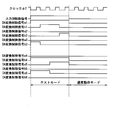
- FIG. 7 shows an example of state transition in the sampling period and the amplification period in the test mode. That is, the control states of the voltage supply unit 8, the auxiliary voltage supply unit 18, and the switch 16 and the value of the analog output signal Vout output from the operational amplifier 9 with respect to the set values of the test signal Vin and the analog reference signal Vdac are shown. .
- the main, auxiliary, and S columns in the column of the voltage supply unit indicate the control states of the voltage supply unit 8, the auxiliary voltage supply unit 18, and the switch 16, respectively. “0” selects 0 V, “+1” selects + Vref, and “ ⁇ 1” selects ⁇ Vref.
- FIG. 8 shows the state of the remainder calculation unit in the normal operation mode and the state of the remainder calculation unit in the state transition example in the case of the test points P1 and P2 (test modes 1 and 2) shown in FIG.
- the predetermined reference voltage selected in the voltage supply unit 8 and the auxiliary voltage supply unit 18 is supplied as a test signal to the remainder operation unit during the sampling period, Similarly, a predetermined analog reference signal can be supplied to the remainder operation unit during the amplification period.
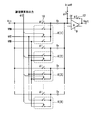
- FIG. 9 is a block diagram showing the configuration of the DA conversion control unit 14b shown in FIG.
- the DA conversion control unit 14b is configured of seven selection control units 19a to 19g.
- the selection control units 19a to 19c respectively output signals for controlling the on / off of the three switches of the voltage supply unit 8.
- the selection control units 19 d to 19 f respectively output signals for controlling on / off of the three switches of the auxiliary voltage supply unit 18.
- the selection control unit 19 g outputs a signal that controls the on / off of the switch 16.
- the specific configuration is described only for the selection control unit 19a.
- the selection control unit 19 a includes a selection circuit 20, an EOR gate 21, and an AND gate 22.
- the configurations of the other selection control units 19b to 19g are the same.
- the DA conversion control signals a1 to a6 input to the selection control units 19a to 19g are signals for controlling the states of the three switches of the voltage supply unit 8 and the auxiliary voltage supply unit 18 during the sampling period.
- the DA conversion control signals b1 to b6 are signals for controlling the states of the three switches of the voltage supply unit 8 and the auxiliary voltage supply unit 18 in the amplification period, respectively.
- FIG. 10 shows an example of the waveforms of the clock 22, the input SW control signal, and the DA conversion control signals a1 to a6 and b1 to b6.
- the output of the logic operation unit 7 is input to the input terminal A of the selection circuit 20 of the selection control units 19a to 19c. Signals at H level, L level, H level, and H level are input to the input terminals A of the selection circuits 20 of the selection control units 19 d to 19 f, respectively.
- the DA conversion control signals a1 to a6 are input to the input terminal B of the selection circuit 20 of the selection control units 19a to 19f and one input terminal of the EOR gate 21, respectively.
- the DA conversion control signal a1 is input to the input terminal B of the selection circuit 20 of the selection control unit 19g and one input terminal of the EOR gate 21.
- the DA conversion control signals b1 to b6 are input to the input terminal C of the selection circuit 20 of the selection control units 19a to 19f and the other input terminal of the EOR gate 21, respectively.
- An L level signal is input to the input terminal C of the selection circuit 20 of the selection control unit 19 g and the other input terminal of the EOR gate 21.
- the output signal of the EOR gate 21, the clock ⁇ 2, and the input SW control signal are input to the AND gate 22 of the selection control units 19a to 19f.
- An output signal of the AND gate 22 and an input SW control signal are supplied as control signals S0 and S1 of the selection circuit 20.
- the selection circuit 20 of the selection control units 19a to 19f switches and outputs the input signals to the input terminals A to C according to the logic as shown in Table 23 shown in FIG.
- the degree of freedom of the set value of the analog input signal to the operational amplifier 9 can be increased.
- the auxiliary voltage supply unit 18 it becomes possible to supply a test signal having a set value according to the application.
- FIG. 12 is an 8-bit pipelined A / D converter, where the stage 1 [3] of the third stage is the test target, and the digital operation unit 6 calculates using the outputs of the fourth and subsequent stages surrounded by a broken line.
- the output result is as follows.
- FIG. 13 shows the main part of an example of the multi-bit stage.
- the conversion function of three stages of a normal 1.5 bit stage is integrated into one stage.
- the power consumption in the pipeline system is dominated by the power consumption of the operational amplifier present in each stage. It is known that adopting a multi-bit stage configuration can reduce the number of operational amplifiers, which is advantageous for reducing power consumption.
- the voltage supply units 8 [1] to 8 [8] are eight in number and are supplied with the outputs of the logic operation units.
- the voltage supply units 8 [2] to 8 [8] are configured to selectively output a binary reference voltage, and include two switches.
- the reference voltage VRT and the reference voltage VRB are respectively supplied to the input side of each switch.
- voltage supply units 8 [1] to 8 [8] are selectively selected from ternary reference voltages VRM, VRT and VRB, or binary reference voltages VRT and VRB, respectively, according to the logic operation unit output. Output one of the reference voltages.
- the combination of the reference voltages respectively supplied from the voltage supply units 8 [1] to 8 [8] to the eight input capacitors Cs substantially produces a 15 value corresponding to the output of the AD conversion unit 3.
- the analog reference signal Vdac is generated and supplied to the remainder operation unit.
- the value of the analog reference signal Vdac is set such that the operation of the remainder operation unit corresponds to the input / output characteristic based on the 15-value quantization.
- FIG. 14 is a block diagram showing a part of stages constituting a pipelined A / D converter in the present embodiment.
- the configuration of the stage of Embodiment 2 is applied to the configuration of a multi-bit stage similar to that shown in FIG.
- An auxiliary voltage supply unit 8 [c] is added to the configuration of FIG.
- the input SW control unit 13a and the DA conversion control unit 14b are provided to switch between the normal operation mode and the test mode.
- the voltage supply units 8 [1] to 8 [8] and the auxiliary voltage supply unit 8 [c] are provided with three reference voltages VRM, VRT and VRB, or two reference voltages according to the output of the logic operation unit. One of the reference voltages is selectively output from VRT and VRB.
- the columns 1 to 8 and the column c in the column of the voltage supply unit indicate the control states of the voltage supply units 8 [1] to 8 [8] and the auxiliary voltage supply unit 8 [c], respectively. “0” is to select VRM, “+1” is to select + Vref, and “ ⁇ 1” is to select ⁇ Vref.
- the configuration of the present invention is applied to the configuration of the multi-bit stage, and the test signal supplied to the stage for various tests is separated from the test signal line separately from the line for normal operation. It is possible to input a test signal on a small scale without providing it.
- the pipeline A / D converter of the present invention can supply a test signal with high accuracy, and can suppress an increase in circuit scale. Therefore, pipeline A / D used in the AV field or information communication field etc. Useful for D-converters.
Landscapes
- Engineering & Computer Science (AREA)
- Theoretical Computer Science (AREA)
- Analogue/Digital Conversion (AREA)
Priority Applications (2)
| Application Number | Priority Date | Filing Date | Title |
|---|---|---|---|
| US12/935,387 US8203474B2 (en) | 2008-03-31 | 2009-03-03 | Pipeline A/D converter |
| CN200980111563.5A CN102067455B (zh) | 2008-03-31 | 2009-03-03 | 流水线a/d转换器 |
Applications Claiming Priority (2)
| Application Number | Priority Date | Filing Date | Title |
|---|---|---|---|
| JP2008-091992 | 2008-03-31 | ||
| JP2008091992A JP2009246752A (ja) | 2008-03-31 | 2008-03-31 | パイプラインa/d変換器 |
Publications (1)
| Publication Number | Publication Date |
|---|---|
| WO2009122656A1 true WO2009122656A1 (ja) | 2009-10-08 |
Family
ID=41135065
Family Applications (1)
| Application Number | Title | Priority Date | Filing Date |
|---|---|---|---|
| PCT/JP2009/000959 Ceased WO2009122656A1 (ja) | 2008-03-31 | 2009-03-03 | パイプラインa/d変換器 |
Country Status (4)
| Country | Link |
|---|---|
| US (1) | US8203474B2 (https=) |
| JP (1) | JP2009246752A (https=) |
| CN (1) | CN102067455B (https=) |
| WO (1) | WO2009122656A1 (https=) |
Cited By (2)
| Publication number | Priority date | Publication date | Assignee | Title |
|---|---|---|---|---|
| WO2011104786A1 (ja) * | 2010-02-26 | 2011-09-01 | 国立大学法人東京工業大学 | パイプライン型a/dコンバータおよびa/d変換方法、ならびにダイナミック型差動増幅器 |
| JP5515126B2 (ja) * | 2010-02-26 | 2014-06-11 | 国立大学法人東京工業大学 | パイプライン型a/dコンバータおよびa/d変換方法、ならびにダイナミック型差動増幅器 |
Families Citing this family (4)
| Publication number | Priority date | Publication date | Assignee | Title |
|---|---|---|---|---|
| CN102684695B (zh) * | 2011-03-16 | 2016-03-02 | 承景科技股份有限公司 | 用于管线式模拟至数字转换器的乘积数字至模拟转换器 |
| JP5811153B2 (ja) * | 2013-09-20 | 2015-11-11 | 株式会社デンソー | A/d変換装置 |
| CN105281767A (zh) * | 2014-06-04 | 2016-01-27 | 中国科学院半导体研究所 | 算法式模数转换器 |
| CN109728817B (zh) * | 2017-10-27 | 2022-10-14 | 瑞昱半导体股份有限公司 | 流水线式模拟数字转换器 |
Citations (3)
| Publication number | Priority date | Publication date | Assignee | Title |
|---|---|---|---|---|
| JP2004222274A (ja) * | 2002-12-27 | 2004-08-05 | Thine Electronics Inc | アナログ/ディジタル変換器及び電子回路 |
| JP2006080717A (ja) * | 2004-09-08 | 2006-03-23 | Matsushita Electric Ind Co Ltd | パイプラインa/d変換器およびその出力補正方法 |
| JP2006109403A (ja) * | 2004-09-07 | 2006-04-20 | Sharp Corp | デジタル補正アナログ/デジタル変換器 |
Family Cites Families (13)
| Publication number | Priority date | Publication date | Assignee | Title |
|---|---|---|---|---|
| US5784016A (en) | 1995-05-02 | 1998-07-21 | Texas Instruments Incorporated | Self-calibration technique for pipe line A/D converters |
| DE10152119A1 (de) * | 2001-10-23 | 2003-04-30 | Basf Ag | Verbessertes Verfahren zur Herstellung von Isocyanaten |
| DE10255354B3 (de) * | 2002-11-27 | 2004-03-04 | Infineon Technologies Ag | A/D-Wandler mit minimiertem Umschaltfehler |
| US7002507B2 (en) * | 2003-09-25 | 2006-02-21 | Sanyo Electric Co., Ltd. | Pipelined and cyclic analog-to-digital converters |
| JP2005354627A (ja) * | 2004-06-14 | 2005-12-22 | Matsushita Electric Ind Co Ltd | パイプラインa/d変換器 |
| JP2006067201A (ja) | 2004-08-26 | 2006-03-09 | Matsushita Electric Ind Co Ltd | パイプラインa/d変換器およびその出力誤差補正方法 |
| US7187310B2 (en) * | 2005-03-04 | 2007-03-06 | Kamal El-Sankary | Circuit calibration using voltage injection |
| TWI266486B (en) * | 2005-06-08 | 2006-11-11 | Via Tech Inc | Cyclic pipeline analog to digital converter |
| JP4684028B2 (ja) | 2005-07-04 | 2011-05-18 | パナソニック株式会社 | パイプラインa/d変換器 |
| CN200997595Y (zh) * | 2006-12-07 | 2007-12-26 | 深圳艾科创新微电子有限公司 | 新型模数转换器结构 |
| JP4934531B2 (ja) * | 2007-07-11 | 2012-05-16 | 株式会社日立製作所 | アナログデジタル変換器及びその制御方法並びに無線トランシーバ回路 |
| JP4720842B2 (ja) * | 2008-03-27 | 2011-07-13 | セイコーエプソン株式会社 | パイプライン型a/d変換器 |
| CN102177658B (zh) * | 2008-10-13 | 2014-04-09 | 集成装置技术公司 | 开关电容器流水线级 |
-
2008
- 2008-03-31 JP JP2008091992A patent/JP2009246752A/ja not_active Withdrawn
-
2009
- 2009-03-03 CN CN200980111563.5A patent/CN102067455B/zh not_active Expired - Fee Related
- 2009-03-03 WO PCT/JP2009/000959 patent/WO2009122656A1/ja not_active Ceased
- 2009-03-03 US US12/935,387 patent/US8203474B2/en active Active
Patent Citations (3)
| Publication number | Priority date | Publication date | Assignee | Title |
|---|---|---|---|---|
| JP2004222274A (ja) * | 2002-12-27 | 2004-08-05 | Thine Electronics Inc | アナログ/ディジタル変換器及び電子回路 |
| JP2006109403A (ja) * | 2004-09-07 | 2006-04-20 | Sharp Corp | デジタル補正アナログ/デジタル変換器 |
| JP2006080717A (ja) * | 2004-09-08 | 2006-03-23 | Matsushita Electric Ind Co Ltd | パイプラインa/d変換器およびその出力補正方法 |
Cited By (6)
| Publication number | Priority date | Publication date | Assignee | Title |
|---|---|---|---|---|
| WO2011104786A1 (ja) * | 2010-02-26 | 2011-09-01 | 国立大学法人東京工業大学 | パイプライン型a/dコンバータおよびa/d変換方法、ならびにダイナミック型差動増幅器 |
| WO2011104761A1 (ja) * | 2010-02-26 | 2011-09-01 | 国立大学法人東京工業大学 | パイプライン型a/dコンバータおよびa/d変換方法 |
| CN102844987A (zh) * | 2010-02-26 | 2012-12-26 | 国立大学法人东京工业大学 | 流水线式a/d转换器和a/d转换方法、以及动态式差动放大器 |
| JP5515126B2 (ja) * | 2010-02-26 | 2014-06-11 | 国立大学法人東京工業大学 | パイプライン型a/dコンバータおよびa/d変換方法、ならびにダイナミック型差動増幅器 |
| US8947287B2 (en) | 2010-02-26 | 2015-02-03 | Tokyo Institute Of Technology | Pipeline A/D converter and A/D converting method |
| CN102844987B (zh) * | 2010-02-26 | 2015-09-02 | 国立大学法人东京工业大学 | 流水线式a/d转换器和a/d转换方法、以及动态式差动放大器 |
Also Published As
| Publication number | Publication date |
|---|---|
| CN102067455B (zh) | 2013-07-17 |
| JP2009246752A (ja) | 2009-10-22 |
| US8203474B2 (en) | 2012-06-19 |
| US20110025536A1 (en) | 2011-02-03 |
| CN102067455A (zh) | 2011-05-18 |
Similar Documents
| Publication | Publication Date | Title |
|---|---|---|
| JP4720842B2 (ja) | パイプライン型a/d変換器 | |
| KR100824793B1 (ko) | 기준 전압을 스스로 공급하는 파이프라인 구조의 아날로그디지털 컨버터 | |
| US6653966B1 (en) | Subranging analog to digital converter with multi-phase clock timing | |
| US8791845B2 (en) | Circuitry and method for reducing area and power of a pipelince ADC | |
| KR900008820B1 (ko) | 아날로그/디지탈변환기 | |
| US7911370B2 (en) | Pipeline analog-to-digital converter with programmable gain function | |
| JP5117451B2 (ja) | スイッチトキャパシタ回路、およびアナログデジタル変換器 | |
| JP4480744B2 (ja) | アナログデジタル変換器 | |
| WO2009122656A1 (ja) | パイプラインa/d変換器 | |
| US7224306B2 (en) | Analog-to-digital converter in which settling time of amplifier circuit is reduced | |
| US20050068219A1 (en) | Analog-to-digital converter having cyclic configuration | |
| JP2009027281A (ja) | サンプルホールド回路およびパイプラインad変換器 | |
| EP2338229B1 (en) | Switched-capacitor pipeline stage | |
| JP5186981B2 (ja) | パイプライン型a/d変換器 | |
| US7847713B2 (en) | Algorithmic analog-to-digital converter | |
| US7348916B2 (en) | Pipeline A/D converter and method of pipeline A/D conversion | |
| JP2006279936A (ja) | アナログデジタル変換器 | |
| JP4681622B2 (ja) | Ad変換器 | |
| US7414563B2 (en) | Analog-to-digital converter with a plurality of conversions | |
| JP2006033304A (ja) | スイッチトキャパシタ回路及びパイプラインa/d変換器 | |
| JP2005086695A (ja) | アナログ−デジタル変換回路 | |
| JP5154683B1 (ja) | 増幅回路およびa/d変換器 | |
| JP2003032112A (ja) | アナログ−デジタル変換回路およびその直流バイアス電圧発生方法 | |
| JP2009218694A (ja) | パイプラインa/d変換器およびディジタルカメラ | |
| JP2017212523A (ja) | 逐次比較型a/dコンバータ |
Legal Events
| Date | Code | Title | Description |
|---|---|---|---|
| WWE | Wipo information: entry into national phase |
Ref document number: 200980111563.5 Country of ref document: CN |
|
| 121 | Ep: the epo has been informed by wipo that ep was designated in this application |
Ref document number: 09727731 Country of ref document: EP Kind code of ref document: A1 |
|
| WWE | Wipo information: entry into national phase |
Ref document number: 12935387 Country of ref document: US |
|
| NENP | Non-entry into the national phase |
Ref country code: DE |
|
| 122 | Ep: pct application non-entry in european phase |
Ref document number: 09727731 Country of ref document: EP Kind code of ref document: A1 |