WO2009113441A1 - シリコン単結晶引上装置及びシリコン単結晶の製造方法 - Google Patents
シリコン単結晶引上装置及びシリコン単結晶の製造方法 Download PDFInfo
- Publication number
- WO2009113441A1 WO2009113441A1 PCT/JP2009/054152 JP2009054152W WO2009113441A1 WO 2009113441 A1 WO2009113441 A1 WO 2009113441A1 JP 2009054152 W JP2009054152 W JP 2009054152W WO 2009113441 A1 WO2009113441 A1 WO 2009113441A1
- Authority
- WO
- WIPO (PCT)
- Prior art keywords
- single crystal
- silicon single
- melt
- sample chamber
- sublimable dopant
- Prior art date
Links
Images

Classifications
-
- C—CHEMISTRY; METALLURGY
- C30—CRYSTAL GROWTH
- C30B—SINGLE-CRYSTAL GROWTH; UNIDIRECTIONAL SOLIDIFICATION OF EUTECTIC MATERIAL OR UNIDIRECTIONAL DEMIXING OF EUTECTOID MATERIAL; REFINING BY ZONE-MELTING OF MATERIAL; PRODUCTION OF A HOMOGENEOUS POLYCRYSTALLINE MATERIAL WITH DEFINED STRUCTURE; SINGLE CRYSTALS OR HOMOGENEOUS POLYCRYSTALLINE MATERIAL WITH DEFINED STRUCTURE; AFTER-TREATMENT OF SINGLE CRYSTALS OR A HOMOGENEOUS POLYCRYSTALLINE MATERIAL WITH DEFINED STRUCTURE; APPARATUS THEREFOR
- C30B15/00—Single-crystal growth by pulling from a melt, e.g. Czochralski method
- C30B15/02—Single-crystal growth by pulling from a melt, e.g. Czochralski method adding crystallising materials or reactants forming it in situ to the melt
- C30B15/04—Single-crystal growth by pulling from a melt, e.g. Czochralski method adding crystallising materials or reactants forming it in situ to the melt adding doping materials, e.g. for n-p-junction
-
- C—CHEMISTRY; METALLURGY
- C30—CRYSTAL GROWTH
- C30B—SINGLE-CRYSTAL GROWTH; UNIDIRECTIONAL SOLIDIFICATION OF EUTECTIC MATERIAL OR UNIDIRECTIONAL DEMIXING OF EUTECTOID MATERIAL; REFINING BY ZONE-MELTING OF MATERIAL; PRODUCTION OF A HOMOGENEOUS POLYCRYSTALLINE MATERIAL WITH DEFINED STRUCTURE; SINGLE CRYSTALS OR HOMOGENEOUS POLYCRYSTALLINE MATERIAL WITH DEFINED STRUCTURE; AFTER-TREATMENT OF SINGLE CRYSTALS OR A HOMOGENEOUS POLYCRYSTALLINE MATERIAL WITH DEFINED STRUCTURE; APPARATUS THEREFOR
- C30B29/00—Single crystals or homogeneous polycrystalline material with defined structure characterised by the material or by their shape
- C30B29/02—Elements
- C30B29/06—Silicon
-
- Y—GENERAL TAGGING OF NEW TECHNOLOGICAL DEVELOPMENTS; GENERAL TAGGING OF CROSS-SECTIONAL TECHNOLOGIES SPANNING OVER SEVERAL SECTIONS OF THE IPC; TECHNICAL SUBJECTS COVERED BY FORMER USPC CROSS-REFERENCE ART COLLECTIONS [XRACs] AND DIGESTS
- Y10—TECHNICAL SUBJECTS COVERED BY FORMER USPC
- Y10T—TECHNICAL SUBJECTS COVERED BY FORMER US CLASSIFICATION
- Y10T117/00—Single-crystal, oriented-crystal, and epitaxy growth processes; non-coating apparatus therefor
- Y10T117/10—Apparatus
- Y10T117/1024—Apparatus for crystallization from liquid or supercritical state
- Y10T117/1032—Seed pulling
Definitions
- the present invention relates to a silicon single crystal pulling apparatus and a silicon single crystal manufacturing method. More specifically, the present invention relates to a silicon single crystal pulling apparatus that pulls a doped silicon single crystal from a melt by the Czochralski method and a method for manufacturing the silicon single crystal.
- the CZ (Czochralski) method is a crystal growth method in which a melt is stored in a crucible in a pulling furnace, and a silicon single crystal is pulled from the melt by a pulling mechanism and grown.
- a dopant such as arsenic, red phosphorus, and antimony
- the sample chamber containing the sublimable dopant is lowered to a predetermined position above the melt in the pulling furnace, and the sublimable dopant is added by the radiant heat radiated from the melt.
- a method is employed in which a sublimable dopant that has been heated and sublimated and turned into a gas by sublimation is introduced into the melt.
- the open end of the supply pipe is disposed above the melt, and an inert gas such as argon gas is used.
- an inert gas such as argon gas
- a method of spraying a dopant conveyed by a carrier gas consisting of from a supply pipe toward a melt can be mentioned.
- a dope tube is disposed at a position where it does not interfere with the pulling mechanism, the dope tube is lowered to a position above the upper surface of the quartz crucible, and is accommodated by radiant heat radiated from the melt at that position.
- the specific resistance range is discontinuously different in the growth axis direction by dissolving the dopant in the part and further lowering the container to a position where it is immersed in the melt, and then introducing the dissolved dopant from the open surface of the dope tube into the melt.
- Patent Document 2 a granular dopant is put in a sealed chamber having an open upper end of a supply pipe in the center, and the open lower end of the supply pipe is immersed in silicon melt to evaporate the dopant.
- An invention of a feed tube assembly for introducing dopant into a melt using pressure is described.
- JP 2005-336020 A Special table 2003-532611 gazette
- N ++ type silicon single crystal is an N type silicon single crystal having a specific resistance value smaller than 0.01 ⁇ cm.
- An object of the present invention is to grow a silicon single crystal having a desired resistivity, to which a sublimable dopant is surely added, without depending on the length of time until the first half of the straight body of the silicon single crystal is formed.
- An object of the present invention is to provide a silicon single crystal pulling apparatus and a method for manufacturing a silicon single crystal.
- the present inventors have conducted various studies on a silicon single crystal pulling apparatus that pulls a silicon single crystal doped with a sublimable dopant at a high concentration from the melt.
- the present inventors can prevent the radiant heat in the pulling furnace from affecting the sublimable dopant in the sample chamber. It has been found that the vaporization of the sublimable dopant until the blocking is canceled, and the present invention has been completed.
- a silicon single crystal pulling apparatus that pulls a silicon single crystal from a melt by the Czochralski method, and a pulling furnace and a sample chamber that is attached to the pulling furnace and contains a sublimable dopant. And a shielding mechanism for thermally shutting off the pulling furnace and the sample chamber, and a supply means for supplying the sublimable dopant to the melt after releasing the shielding mechanism. Silicon single crystal pulling device.
- the radiant heat in the pulling furnace affects the sublimable dopant in the sample chamber. Disappear. Therefore, vaporization of the sublimable dopant until the shielding mechanism is released and the sublimable dopant is supplied to the melt is prevented. Therefore, it is possible to grow a silicon single crystal having a desired resistivity to which a sublimable dopant is surely added without depending on the time required for forming the first half of the straight body portion of the silicon single crystal.
- the space between the sample chamber and the pulling furnace is thermally blocked by the shielding mechanism, and the influence of radiant heat in the pulling furnace on the sublimable dopant. Then, the sample chamber can be opened and a sublimable dopant can be introduced. For this reason, it is possible to avoid doping during the period from when the sublimable dopant is set to when it is introduced and until the first half of the straight body of the silicon single crystal is formed. Further, during the growth of the straight body portion of the crystal where the crystal growth is stabilized, a high concentration sublimable dopant can be repeatedly introduced through the sample chamber a plurality of times.
- the diameter of the aperture can be increased, the aperture portion can withstand a larger load, and the N ++ type silicon single crystal can be further increased in size.
- the silicon single crystal pulling apparatus further includes a dope tube that stores the sublimable dopant, and as a supply means, a supply tube that supplies the vaporized sublimable dopant connected to the dope tube to the melt, and a sample. And transfer means for transferring the dope tube from the chamber to the supply tube.
- the liquid vibration of the melt, the decrease in the liquid temperature, and the change in the convection are reduced by spraying the sublimable dopant on the melt through the supply means. Therefore, crystal breakage of the grown silicon single crystal can be reduced.
- a silicon single crystal characterized in that, after blocking, a sublimable dopant is accommodated in the sample chamber to seal the sample chamber, and then the shielding mechanism is opened to supply the sublimable dopant to the melt. Manufacturing method.
- the radiant heat in the pulling furnace does not affect the sublimable dopant in the sample chamber by thermally blocking the inside of the pulling furnace and the inside of the sample chamber using a shielding mechanism. , Vaporization of the sublimable dopant is prevented. Therefore, a predetermined amount of sublimable dopant can be reliably added to the melt at a desired timing. In addition, it is possible to grow a silicon single crystal having a specific resistance profile that suddenly changes from a desired position of the crystal to a doped crystal position with respect to the growth axis direction.
- the dopant stored in the dope tube is stored in the sample chamber, and after the shielding mechanism is opened, the dope tube is transferred by the transfer means and connected to the supply tube in the pulling furnace and melted through the supply tube. It is preferable to spray a dopant on the liquid. This eliminates the need to install the dope tube on the seed shaft in the pulling furnace. Further, since the work time required for installing and removing the dope tube is shortened, the work time required for removing and attaching the sublimable dopant can be shortened.
- the addition of a high concentration of sublimable dopant from the shoulder portion of the crystal to the front half of the straight body portion is suppressed, and the concentration of the sublimable dopant increases from the front half of the straight body portion to the tail portion.
- An added silicon single crystal is manufactured. Since the high concentration of sublimable dopant is suppressed from the shoulder of the crystal, where the crystal growth is likely to be unstable, to the first half of the straight body, the crystal growth in this part is stabilized, resulting in higher yields. Enables the production of silicon single crystals.
- the specific resistance value of the silicon single crystal becomes smaller than 0.01 ⁇ cm by adding a sublimable dopant consisting of at least one of the group consisting of arsenic, red phosphorus and antimony at a high concentration. . For this reason, an N ++ type silicon single crystal can be manufactured.
- silicon doped with a sublimable dopant at a desired timing without depending on the time required for forming the shoulder portion of the silicon single crystal to the first half of the straight body portion or the length of the pulling length.
- Single crystal growth begins. For this reason, the crystal state up to the first half of the straight body portion can be reliably improved, and the crystal state of the silicon single crystal doped with a sublimable dopant that is subsequently grown can be improved.
- the radiant heat in the pulling furnace does not affect the sublimable dopant in the sample chamber, and the shielding is performed.
- the vaporization of the sublimable dopant until the mechanism is released is prevented. For this reason, it is possible to grow a silicon single crystal having a desired resistivity, to which a sublimable dopant is surely added, without depending on the length of time until the first half of the straight body portion of the silicon single crystal is formed.
- a silicon single crystal pulling apparatus and a method for producing a silicon single crystal can be provided.
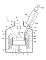
- Sectional drawing of the silicon single crystal pulling apparatus of this embodiment is shown.
- the principal part perspective view of the silicon single crystal pulling apparatus of this embodiment is shown.
- a silicon single crystal pulling apparatus and a silicon single crystal manufacturing method include a pulling furnace, a sample chamber that is externally attached to the pulling furnace and contains a sublimable dopant, a pulling furnace, and a sample chamber. And a supply mechanism for supplying a sublimable dopant to the melt after the shield mechanism is released.
- the first embodiment of the present invention is a silicon single crystal pulling apparatus.
- FIG. 1 is a cross-sectional view of the silicon single crystal pulling apparatus according to the present embodiment
- FIG. 2 is a perspective view of a main part of the silicon single crystal pulling apparatus according to the present embodiment.
- the silicon single crystal pulling apparatus 1 of this embodiment includes a pulling furnace (chamber) 2 that can be used for crystal growth by the CZ method.
- a crucible 3 for containing a melt 5 obtained by melting a raw material made of polycrystalline silicon (Si).
- the crucible 3 is made of, for example, quartz.
- a heater 9 for heating and melting the raw material in the crucible 3.
- a heat insulating cylinder 13 is provided between the heater 9 and the inner wall of the pulling furnace 2.
- the pulling mechanism 4 includes a pulling cable 4a and a seed crystal holder 4b at the tip of the pulling cable 4a.
- the seed crystal is held by the seed crystal holder 4b.
- the raw material is put into the crucible 3 and heated using the heater 9 to melt the raw material into the melt 5.
- the pulling cable 4a is lowered and the seed crystal held by the seed crystal holder 4b is immersed in the melt 5.
- the pulling cable 4 a is raised, and a silicon single crystal (silicon single crystal ingot) 6 is pulled from the melt 5 to grow.
- the crucible 3 is rotated by the rotating shaft 10.
- the pulling cable 4 a of the pulling mechanism 4 is rotated in the same direction as the rotating direction of the rotating shaft 10 or in the opposite direction.
- the rotating shaft 10 can also be driven in the vertical direction, and the crucible 3 can be moved up and down to an arbitrary upward position.
- the inside of the pulling furnace 2 is depressurized to a vacuum state (for example, about several tens of Torr) while blocking the outside air. Further, while supplying the argon gas 7 as an inert gas into the pulling furnace 2, the argon gas 7 is exhausted from the pulling furnace 2 using a pump. By allowing the argon gas 7 to flow inside the pulling furnace 2, the vapor generated inside the pulling furnace 2 can be removed together with the argon gas 7 to the outside of the pulling furnace 2.
- the supply flow rate of the argon gas 7 at this time can be set according to each process of crystal growth.
- a heat shielding plate 8 (gas rectifying cylinder) is provided above the crucible 3 and around the silicon single crystal 6.
- the heat shielding plate 8 guides the argon gas 7 supplied from above the pulling furnace 2 to the center of the melt surface 5a, and further guides it to the peripheral portion of the melt surface 5a via the melt surface 5a.
- the argon gas 7 is discharged together with the evaporated material from the melt 5 from an exhaust port provided in the lower part of the pulling furnace 2. Thereby, the gas flow velocity on the liquid surface can be stabilized, and oxygen evaporated from the melt 5 can be kept in a stable state.
- the heat shielding plate 8 also has an action of blocking the radiant heat generated in the high-temperature portion such as the crucible 3, the melt 5 and the heater 9 with respect to the seed crystal and the growing silicon single crystal 6.
- the heat shielding plate 8 also has an action to prevent impurities (for example, silicon oxide) generated in the pulling furnace 2 from adhering to the silicon single crystal 6 and inhibiting single crystal growth.
- impurities for example, silicon oxide
- the size of the distance D between the lower end of the heat shielding plate 8 and the melt surface 5a may be adjusted by the vertical movement of the crucible 3 or by the vertical movement of the heat shielding plate 8 by the lifting device. Good.
- the sample chamber 20 contains a sublimable dopant (impurity) 23 to be doped into the silicon single crystal 6 to be grown.
- the sample chamber 20 is externally attached to the flange portion of the pulling furnace 2 through a shielding mechanism 24 described later.
- the sublimable dopant 23 accommodated in the sample chamber 20 arsenic As, red phosphorus P, or antimony, which is a sublimable dopant for N type for imparting N-type electrical characteristics to the silicon single crystal 6. Sb is mentioned.
- arsenic As and red phosphorus P are sublimable dopants that can be sublimated, by using them as the sublimable dopant 23, they can be vaporized from a solid phase to a gas phase at a relatively low temperature.
- the material of the dope tube 21 may be a material that can withstand high temperatures caused by melt radiant heat, specifically, quartz.
- the sample chamber 20 is preferably provided with a vacuum pump and an argon gas line.
- a vacuum pump and an argon gas line By providing the vacuum pump and the argon gas line, the pressure inside the sample chamber 20 is reduced independently of the pulling furnace 2 or returned to normal pressure. For this reason, when the gate valve is opened or the dope tube 21 is removed, a sudden pressure change in the sample chamber 20 can be reduced.
- the sample chamber 20 is preferably provided with a cooling mechanism.
- the cooling mechanism By providing the cooling mechanism, the dope tube 21 heated in the pulling furnace 2 is efficiently cooled by the combined use of the cooling mechanism and the argon gas. For this reason, exchange of dope tube 21 can be made smoother.
- a pipe having flanges at both ends may be interposed between the sample chamber 20 and the pulling furnace 2.
- the cooling mechanism can be provided in the piping similarly to the sample chamber 20, or a small window can be provided in the piping. In particular, it is possible to easily confirm that the sublimable dopant 23 is reliably charged by providing a small window in the pipe.
- the shielding mechanism 24 thermally shuts off the pulling furnace 2 and the sample chamber 20 and is provided between the pulling furnace 2 and the sample chamber 20.
- the radiant heat and atmosphere in the pulling furnace 2 are thermally blocked by the shielding mechanism 24, so that a desired amount of the sublimable dopant 23 can be vaporized at a desired timing.
- the sublimation dopant 23 can be introduced from the sample chamber 20 by opening the shielding mechanism 24 during crystal growth.
- a slide gate valve can be preferably used. Since the space in the stroke direction of the shielding mechanism 24 is reduced by using the slide gate valve, the distance for transferring the sublimable dopant 23 from the sample chamber 20 can be further shortened. At this time, it is more preferable to use a cooling mechanism for the shielding mechanism 24. By using the cooling mechanism, the shielding mechanism 24 is not deteriorated by the heat from the pulling furnace 2, so that the pulling furnace 2 and the sample chamber 20 can be reliably thermally shut off.
- the shielding mechanism 24 While the shielding mechanism 24 is closed, the radiant heat in the pulling furnace 2 does not reach the sublimable dopant 23 in the sample chamber 20, and the sublimable dopant 23 is not vaporized. Therefore, during the period from when the growth of the silicon single crystal 6 is started until the shielding mechanism 24 is opened for the first time, the growing silicon single crystal 6 can be in an additive-free state containing no sublimable dopant 23.
- the shielding mechanism 24 is opened at the timing when the silicon single crystal 6 starts to be doped with the sublimable dopant 23, that is, when the silicon single crystal 6 grows from the shoulder portion to the first half of the straight body portion.
- the sublimable dopant 23 is stored in a predetermined position in the sample chamber 20, the door of the sample chamber 20 is closed, and then the vacuum pump on the sample chamber 20 side is operated. The inside of the pulling furnace 2 and the inside of the sample chamber 20 are adjusted and then opened.
- the shielding mechanism 24 is opened at a timing when the silicon single crystal 6 grows from the shoulder portion to the front half portion of the straight body portion, and the N-type sublimation dopant 23 is doped at a high concentration, so that from the shoulder portion to the straight body portion. Up to the first half, the sublimation dopant 23 is not added, and from the first half of the straight body portion to the tail portion, the sublimation dopant 23 is added at a high concentration and low resistivity.
- the silicon single crystal 6 that can obtain the N ++ type electrical characteristics can be manufactured.
- the timing of introducing the sublimable dopant 23 that gives the N-type electrical characteristics to the silicon single crystal 6 is accurately controlled. For this reason, even if it takes time to grow the first half of the straight body of the silicon single crystal 6, it is possible to reduce the collapse of the crystal.
- This shielding mechanism 24 can be closed not only at the timing when the growth of the silicon single crystal 6 is finished, but also at the timing when all the sublimable dopants 23 are added even during the crystal growth. After closing the shielding mechanism 24, the argon gas 7 is introduced into the sample chamber 20 to return the pressure inside the sample chamber 20 to atmospheric pressure, and then the door of the sample chamber 20 is opened to sublimate the dopant 23. Can be charged repeatedly.
- the supply means is means for supplying the sublimable dopant 23 to the melt 5 after releasing the thermal block between the pulling furnace 2 and the sample chamber 20 by the shielding mechanism 24.
- This supply means what has the following transfer means 25 and the supply pipe
- the transfer means 25 transfers the dope tube 21 so as to be connected to a supply tube 22 to be described later, and includes, for example, a wire lifting unit 25a and lifting rails 25b and 25c.
- the wire elevating unit 25a is a mechanism for moving the dope tube 21 up and down with a wire, and drives the winding drum by a motor to adjust the height position of the dope tube 21 through the wire. At this time, the driving of the motor in the wire lifting / lowering unit 25 a is preferably controlled by the height position of the dope tube 21 and the open / closed state of the shielding mechanism 24.
- the elevating rails 25b and 25c are provided between the inside of the sample chamber 20 and the supply pipe 22, and define the position where the dope pipe 21 moves up and down.
- the elevating rails 25b and 25c are preferably made of a graphite material. By forming from a graphite material, high heat resistance can be provided, and restrictions on the shapes of the lifting rails 25b and 25c can be further reduced.
- These transfer means 25 are arranged at a position where they do not interfere with the silicon single crystal 6 and the pulling mechanism 4 and are not immersed in the melt 5 as shown in FIG. By disposing at a position that does not interfere with the pulling mechanism 4, the sublimable dopant 23 can be introduced while pulling up the silicon single crystal 6.
- the dope tube 21 in which the sublimable dopant 23 is accommodated descends along the elevating rails 25b and 25c by driving the wire elevating unit 25a. Then, the tip of the dope tube 21 and the supply tube 22 are connected.
- the supply pipe 22 is connected to the dope pipe 21 transferred by the transfer means 25, and guides the sublimable dopant 23 that has been vaporized by receiving radiant heat from the melt 5 or the like to the melt 5.
- the supply pipe 22 is disposed at a position where it does not interfere with the silicon single crystal 6 and the pulling mechanism 4 and is not immersed in the melt 5.
- the silicon single crystal 6 By disposing the silicon single crystal 6 at a position where it does not interfere with the pulling mechanism 4, it is possible to guide the vaporized sublimable dopant 23 to the melt 5 and perform doping during crystal pulling with extremely high accuracy. Can do.
- the supply pipe 22 is arranged at a position not immersed in the melt 5, and the vaporized sublimable dopant 23 is sprayed from the supply pipe 22 to the melt 5, so that the supply pipe 22, the sublimable dopant 23 and the like are applied to the melt 5.
- the supply pipe 22 is arranged at a position where the charging efficiency of the sublimable dopant 23 into the melt 5 is maximized when the sublimable dopant 23 is sprayed onto the melt 5.
- the material of the supply pipe 22 can be a material that can withstand high temperatures due to radiant heat such as melt, and specifically, quartz can be used.
- the sublimable dopant 23 is supplied to the melt 5 by a spraying method.
- the sublimable dopant 23 is added to the melt 5 by using an immersion method in which the supply pipe 22 is immersed in the melt 5. May be supplied.
- a carrier gas introduction pipe (not shown) can be used as necessary.
- the carrier gas introduction tube communicates with the dope tube 21 and introduces a carrier gas for transporting a dopant supplied from a gas supply source (not shown) into the dope tube 21.
- a carrier gas supplied from a gas supply source (not shown) into the dope tube 21.
- the carrier gas introduction pipe is made of, for example, quartz.
- an inert gas such as argon gas is used as the carrier gas.
Landscapes
- Chemical & Material Sciences (AREA)
- Engineering & Computer Science (AREA)
- Crystallography & Structural Chemistry (AREA)
- Materials Engineering (AREA)
- Metallurgy (AREA)
- Organic Chemistry (AREA)
- Crystals, And After-Treatments Of Crystals (AREA)
Abstract
シリコン単結晶の直胴部の前半部までが形成される時間の長短によることなく、昇華性ドーパントが確実に添加された、所望の抵抗率を有するシリコン単結晶を成長することができるシリコン単結晶引上装置及びシリコン単結晶の製造方法を提供する。 このシリコン単結晶引上装置は、チョクラルスキー法により融液からシリコン単結晶を引上げるシリコン単結晶引上装置であって、引上炉と、前記引上炉に外付けされており昇華性ドーパントを収容する試料室と、前記引上炉と前記試料室とを熱的に遮断する遮蔽機構と、前記遮蔽機構の遮断を解除した後に前記昇華性ドーパントを融液に供給する供給手段と、を含んでなる。
Description
本発明は、シリコン単結晶引上装置及びシリコン単結晶の製造方法に関する。より具体的には、ドープされたシリコン単結晶をチョクラルスキー法により融液から引上げるシリコン単結晶引上装置及びシリコン単結晶の製造方法に関する。
CZ(チョクラルスキー)法は、引上炉内のるつぼに融液を貯留し、この融液からシリコン単結晶を引上げ機構によって引上げて成長させる結晶成長法である。
シリコン単結晶にn型の電気的特性を与えるには、砒素、赤リン及びアンチモン等のドーパントをシリコン単結晶に添加する必要がある。これらドーパントをシリコン結晶に添加する方法としては、昇華性ドーパントが収容された試料室を、引上炉内の融液上方の所定位置まで下降し、融液から輻射される輻射熱によって昇華性ドーパントを加熱して昇華させて、昇華によって気体となった昇華性ドーパントを融液に導入する方法が取られている。
気体となったドーパントを融液に導入する方法の1つとしては、特許文献1及び2に示すように、供給管の開口端を融液より上方に配置して、アルゴンガス等の不活性ガスからなるキャリアガスによって搬送されるドーパントを、供給管から融液に向けて吹き付ける方式が挙げられる。また、他の方式としては、供給管を融液に浸漬し、昇華して気体となったドーパントを、供給管を通じて融液に投入する方式が挙げられる。
特許文献1には、引上げ機構と干渉しない位置にドープ管を配置して、ドープ管を石英るつぼの上面よりも上となる位置まで下降させて、その位置で融液から輻射される輻射熱によって収容部内のドーパントを溶解させ、さらに収容容器を融液に浸漬する位置まで下降させて、ドープ管の開放面から溶解されたドーパントを融液に投入し、成長軸方向に不連続に異なる比抵抗範囲をもつシリコン単結晶インゴットを引上げ成長させる発明が記載されている。
特許文献2には、中央に供給管の開放上端部を有するシールされた部屋に粒状のドーパントを入れ、供給管の開放下端部をシリコン融液に浸漬してドーパントを蒸発させ、蒸発したドーパントの圧力を用いてドーパントを融液に導入するための供給管アセンブリの発明が記載されている。
特開2005-336020号公報
特表2003-532611号公報
ここで、低抵抗率で高濃度のN++型の電気的特性が得られるシリコン単結晶インゴットを得るためには、砒素As、赤燐P、アンチモンSb等のN型用のドーパントを高濃度にシリコン単結晶に添加する必要がある。なお、N++型のシリコン単結晶とは、比抵抗値が0.01Ωcmより小さいN型のシリコン単結晶のことである。
しかしながら、こうしたN++型のシリコン単結晶の引上げを行う際に、融液に供給しておくドーパントの濃度を高濃度にすると、結晶の肩部から直胴部の前半部(概ね直径100mm前後となる部分)の間を成長させる際に、結晶の肩部や肩部の下で結晶が崩れやすい問題点があった。また、肩部の形成前に結晶の径を絞って転位を除去しようとしても、ドーパントの濃度を高濃度にすると転位の除去が困難になるため、絞りの部分をより細くし、かつ絞りの部分を長尺化する必要があり、結晶の直胴部の前半部までの成長により多くの時間がかかる問題点があった。
そのため、直胴部の前半部が成長するまではドーパントを昇華させずに保持し、直胴部の前半部が成長してから目的の電気抵抗率になるようにドープする必要がある。しかしながら、結晶の直胴部の前半部までの成長に時間が掛かり過ぎると、直胴部の前半部が形成される前にドーパントが昇華してしまい、所望の電気的特性を有するシリコン単結晶の成長が困難になる問題点があった。
本発明は、こうした実情に鑑みてなされたものである。本発明の課題は、シリコン単結晶の直胴部の前半部までが形成される時間の長短によることなく、昇華性ドーパントが確実に添加された、所望の抵抗率を有するシリコン単結晶を成長させることができるシリコン単結晶引上装置及びシリコン単結晶の製造方法を提供することにある。
本発明者らは、昇華性ドーパントを高濃度でドープしたシリコン単結晶を融液から引上げるシリコン単結晶引上装置につき種々の検討を行った。本発明者らは、引上炉と試料室との間を熱的に遮断する遮蔽機構を設けることにより、引上炉内の輻射熱が試料室内の昇華性ドーパントに影響を及ぼさなくなり、遮蔽機構の遮断を解除するまでの昇華性ドーパントの気化が防止されることを見出し、本発明を完成するに至った。
(1) チョクラルスキー法によりシリコン単結晶を融液から引上げるシリコン単結晶引上装置であって、引上炉と、前記引上炉に外付けされており昇華性ドーパントを収容する試料室と、前記引上炉と前記試料室とを熱的に遮断する遮蔽機構と、前記遮蔽機構の遮断を解除した後に前記昇華性ドーパントを融液に供給する供給手段と、を含むことを特徴とするシリコン単結晶引上装置。
(1)の発明によれば、引上炉の内部と試料室の内部とを熱的に遮断する遮蔽機構を設けることにより、引上炉内の輻射熱が試料室内の昇華性ドーパントに影響を及ぼさなくなる。したがって、遮蔽機構の遮断を解除して昇華性ドーパントを融液に供給するまでの昇華性ドーパントの気化が防止される。そのため、シリコン単結晶の直胴部の前半部までが形成される時間によることなく、昇華性ドーパントが確実に添加された、所望の抵抗率を有するシリコン単結晶を成長させることができる。
また、(1)の発明によれば、遮蔽機構を設けることにより、試料室と引上炉との間を遮蔽機構により熱的に遮断し、昇華性ドーパントへの引上炉内の輻射熱の影響がないようにした上で、試料室を開放して昇華性ドーパントを投入することができる。このため、昇華性ドーパントをセッティングしてから投入するまでの間、及びシリコン単結晶の直胴部の前半部までが形成されるまでの間のドープを回避することができる。また、結晶成長が安定化する結晶の直胴部の成長中に、試料室を通じて、高濃度の昇華性ドーパントを複数回繰り返し投入することが可能になる。
さらに、(1)の発明によれば、シリコン単結晶の直胴部の前半部までが形成されるまでの結晶成長が困難な部分へのドープが回避される。したがって、肩部の形成前における絞りによる転位の除去をより容易にすることができる。そのため、絞り径の大径化が可能になり、絞りの部分がより大きな荷重に耐えられるようになり、N++型のシリコン単結晶をより大型化することができる。
このとき、シリコン単結晶引上装置は、昇華性ドーパントを収納するドープ管をさらに有し、供給手段として、ドープ管と接続して気化した昇華性ドーパントを融液に供給する供給管と、試料室から供給管にドープ管を移送する移送手段と、を含むことが好ましい。結晶成長中にドープ管を移送することにより、シード軸にドープ管をセットする作業、及び、シード軸からドープ管を抜取る作業が省略される。このため、昇華性ドーパントの付け外しに要する作業時間を短縮することができる。
(2) 前記供給手段は、融液に浸漬しない位置に配置されており、気化した前記昇華性ドーパントを融液に吹き付けるものであることを特徴とする(1)記載のシリコン単結晶引上装置。
(2)の発明によれば、供給手段を通じて昇華性ドーパントを融液に吹き付けることにより、融液の液振、液温の低下、及び対流の変化が少なくなる。したがって、成長したシリコン単結晶の結晶崩れを低減することができる。
(3) ドープされたシリコン単結晶をチョクラルスキー法により成長させるシリコン単結晶の製造方法であって、引上炉と前記引上炉に外付けされた試料室とを遮蔽機構により熱的に遮断した後、前記試料室に昇華性ドーパントを収納して前記試料室を密閉し、続いて、前記遮蔽機構を開放して融液に前記昇華性ドーパントを供給することを特徴とするシリコン単結晶の製造方法。
(3)の発明によれば、引上炉内部と試料室内部とを遮蔽機構を用いて熱的に遮断することにより、引上炉内の輻射熱が試料室内の昇華性ドーパントに影響を及ぼさなくなり、昇華性ドーパントの気化が防止される。そのため、所望のタイミングで所定量の昇華性ドーパントを確実に融液に添加することができる。また、結晶の所望の位置から成長軸方向に対してドーピングした結晶位置で比抵抗プロファイルが急激に変化したシリコン単結晶を成長させることができる。
また、(3)の発明によれば、遮断機構を用いて引上炉と試料室を一時的に絶縁することで、結晶成長中でも昇華性ドーパントの収納や交換の作業を行うことが可能になる。
このとき、ドープ管に収納したドーパントを試料室に収納するとともに、遮蔽機構を開放した後、ドープ管を移送手段により移送して引上炉内の供給管に接続し、供給管を介して融液にドーパントを吹き付けることが好ましい。これにより、ドープ管を引上炉内のシード軸に設置する必要がなくなる。また、ドープ管の設置及び取外しに要していた作業時間が短縮されるため、昇華性ドーパントの付け外しに要する作業時間を短縮することができる。
(4) 前記遮蔽機構を開放する前に前記シリコン単結晶の直胴部の前半部までを成長させ、前記遮蔽機構を開放した後に前記シリコン単結晶の直胴部の前半部から後を成長させることを特徴とする(3)記載のシリコン単結晶の製造方法。
(4)の発明によれば、結晶の肩部から直胴部の前半部にかけて昇華性ドーパントの高濃度な添加が抑えられ、直胴部の前半部からテール部にかけて昇華性ドーパントが高濃度に添加されたシリコン単結晶が製造される。結晶の成長が不安定になりやすい結晶の肩部から直胴部の前半部にかけて昇華性ドーパントの高濃度な添加が抑えられるため、この部分での結晶の成長を安定化して、より高い歩留りでのシリコン単結晶の製造を可能にする。
(5) 前記昇華性ドーパントが砒素、赤リン及びアンチモンからなる群のうち少なくとも一種であることを特徴とする(3)又は(4)記載のシリコン単結晶の製造方法。
(5)の発明によれば、昇華性ドーパントとして砒素、赤リン及びアンチモンからなる群のうち少なくとも一種を添加することで、これらの昇華性ドーパントがドナーとして作用する。このため、N型の電気的特性を有するシリコン単結晶を製造することができる。
(6) 昇華性ドーパントを高濃度に添加することを特徴とする(5)記載のシリコン単結晶の製造方法。
(6)の発明によれば、砒素、赤リン及びアンチモンからなる群のうち少なくとも一種からなる昇華性ドーパントを高濃度に添加することにより、シリコン単結晶の比抵抗値が0.01Ωcmより小さくなる。このため、N++型シリコン単結晶を製造することができる。
(7) (3)から(6)のいずれか記載のシリコン単結晶の製造方法により製造されたシリコン単結晶インゴット。
(7)の発明によれば、シリコン単結晶の肩部から直胴部の前半部までが形成される時間や引上げ長さの長短によることなく、所望のタイミングで昇華性ドーパントがドープされたシリコン単結晶の成長が開始される。このため、直胴部の前半部までの結晶状態を確実に改善することができ、それに続いて成長する昇華性ドーパントのドープされたシリコン単結晶の結晶状態もより良いものにすることができる。
本発明によれば、引上炉の内部と試料室の内部とを熱的に遮断する遮蔽機構を設けることにより、引上炉内の輻射熱が試料室内の昇華性ドーパントに影響を及ぼさなくなり、遮蔽機構の遮断を解除するまでの昇華性ドーパントの気化が防止される。このため、シリコン単結晶の直胴部の前半部までが形成される時間の長短によることなく、昇華性ドーパントが確実に添加された、所望の抵抗率を有するシリコン単結晶を成長させることができるシリコン単結晶引上装置及びシリコン単結晶の製造方法を提供することができる。
以下、本発明について具体的に説明する。
本発明のシリコン単結晶引上装置及びシリコン単結晶の製造方法は、引上炉と、引上炉に外付けされており昇華性ドーパントを収容する試料室と、引上炉と試料室とを熱的に遮断する遮蔽機構と、遮蔽機構の遮断を解除した後に昇華性ドーパントを融液に供給する供給手段と、を含むことを特徴とする。
以下、必要に応じて図1及び図2を参照しながら、本発明のシリコン単結晶引上装置及びシリコン単結晶の製造方法の実施形態について詳細に説明する。なお、本発明は、以下の実施形態に何ら限定されるものではなく、本発明の目的の範囲内において、適宜変更を加えて実施することができる。また、説明が重複する箇所については、適宜説明を省略する場合があるが、発明の趣旨を限定するものではない。
≪シリコン単結晶引上装置≫
本発明の第一の実施形態は、シリコン単結晶引上装置である。図1は本実施形態のシリコン単結晶引上装置の断面図を示し、図2は本実施形態のシリコン単結晶引上装置の要部斜視図を示す。
本発明の第一の実施形態は、シリコン単結晶引上装置である。図1は本実施形態のシリコン単結晶引上装置の断面図を示し、図2は本実施形態のシリコン単結晶引上装置の要部斜視図を示す。
[引上炉]
図1及び図2に示すように、本実施形態のシリコン単結晶引上装置1は、CZ法による結晶成長に用いることのできる引上炉(チャンバ)2を備えている。
図1及び図2に示すように、本実施形態のシリコン単結晶引上装置1は、CZ法による結晶成長に用いることのできる引上炉(チャンバ)2を備えている。
引上炉2の内部には、多結晶シリコン(Si)からなる原料を溶融した融液5を収容する坩堝3が設けられている。坩堝3は、例えば石英で構成されている。坩堝3の周囲には、坩堝3の中にある原料を加熱して溶融するヒータ9が設けられている。このヒータ9と引上炉2の内壁との間には、保温筒13が設けられている。
また、坩堝3の上方には、引上げ機構4が設けられている。引上げ機構4は、引上げ用ケーブル4aと、引上げ用ケーブル4aのその先端にある種結晶ホルダ4bとからなる。この種結晶ホルダ4bによって種結晶が把持される。
ここで、坩堝3の中に原料を入れ、ヒータ9を用いて加熱し、原料を溶融して融液5にする。融液5の溶融状態が安定化したところで、引上げ用ケーブル4aを降下して種結晶ホルダ4bに把持させた種結晶を融液5に浸漬する。種結晶を融液5になじませた後で、引上げ用ケーブル4aを上昇させ、融液5からシリコン単結晶(シリコン単結晶インゴット)6を引上げて成長させる。シリコン単結晶6を成長させる際、坩堝3を回転軸10によって回転させる。それとともに、引上げ機構4の引上げ用ケーブル4aを、回転軸10の回転方向と同じ方向又は逆の方向に回転させる。ここで、回転軸10は鉛直方向にも駆動することができ、坩堝3を任意の上方方向の位置に上下動させることもできる。
このとき、引上炉2の内部は、外気を遮断して真空状態(例えば数十Torr程度)に減圧される。また、引上炉2の内部に、不活性ガスとしてアルゴンガス7を供給しつつ、ポンプを用いて引上炉2の内部からアルゴンガス7を排気する。引上炉2の内部にアルゴンガス7を流通させることにより、引上炉2の内部で発生した蒸発物を、アルゴンガス7ととともに引上炉2の外部に除去することができる。このときのアルゴンガス7の供給流量は、結晶成長の各プロセスによって各々設定することができる。
シリコン単結晶6が成長してくると、融液5の減少によって融液5と坩堝3との接触面積が変化し、坩堝3からの酸素溶解量が変化する。このため、融液5の減少により、引き上げられるシリコン単結晶6中の酸素濃度分布が影響を受ける。そこで、坩堝3の上方及びシリコン単結晶6の周囲に、熱遮蔽板8(ガス整流筒)を設ける。この熱遮蔽板8は、引上炉2の上方より供給されるアルゴンガス7を融液表面5aの中央に導き、さらに融液表面5aを経由して融液表面5aの周縁部に導く。そして、アルゴンガス7は、融液5からの蒸発物とともに、引上炉2の下部に設けた排気口から排出される。それにより、液面上のガス流速を安定化させ、融液5から蒸発する酸素を安定な状態に保つことができる。
また、この熱遮蔽板8は、種結晶及び成長するシリコン単結晶6に対しての、坩堝3、融液5、ヒータ9等の高温部で発生する輻射熱を遮断する作用も有する。また熱遮蔽板8は、引上炉2の中で発生した不純物(例えばシリコン酸化物)等がシリコン単結晶6に付着して単結晶育成が阻害されないようにする作用も有する。ここで、熱遮蔽板8の下端と融液表面5aとの距離Dの大きさは、坩堝3の上下動によって調整してもよく、熱遮蔽板8の昇降装置による上下動によって調整してもよい。
[試料室]
試料室20は、成長させるシリコン単結晶6にドープさせる昇華性ドーパント(不純物)23を収容する。試料室20は、引上炉2のフランジ部に後述する遮蔽機構24を介して外付けされる。ここで、試料室20に収容する昇華性ドーパント23としては、シリコン単結晶6にN型の電気的特性を与えるためのN型用の昇華性ドーパントである、砒素As、赤燐P、又はアンチモンSbが挙げられる。特に、砒素As及び赤燐Pは、昇華可能な昇華性ドーパントであるため、これらを昇華性ドーパント23として用いることにより、比較的低い温度で固相から気相に気化させることができる。
試料室20は、成長させるシリコン単結晶6にドープさせる昇華性ドーパント(不純物)23を収容する。試料室20は、引上炉2のフランジ部に後述する遮蔽機構24を介して外付けされる。ここで、試料室20に収容する昇華性ドーパント23としては、シリコン単結晶6にN型の電気的特性を与えるためのN型用の昇華性ドーパントである、砒素As、赤燐P、又はアンチモンSbが挙げられる。特に、砒素As及び赤燐Pは、昇華可能な昇華性ドーパントであるため、これらを昇華性ドーパント23として用いることにより、比較的低い温度で固相から気相に気化させることができる。
試料室20に昇華性ドーパント23を収容する際には、ドープ管21に昇華性ドーパント23を収納するとともに、このドープ管21を試料室20に収容することが好ましい。ドープ管21を用いることで、試料室20への昇華性ドーパント23の出し入れを容易にするとともに、稼働中の引上炉2への昇華性ドーパント23の投入をより確実に行うことができる。ここで、ドープ管21の材質は、メルト輻射熱による高温に耐えられる材質、具体的には石英を用いることができる。
試料室20には真空ポンプ及びアルゴンガスラインを設けることが好ましい。真空ポンプ及びアルゴンガスラインを設けることで、試料室20の内部の圧力が引上炉2と独立して減圧され、又は常圧に戻される。このため、ゲートバルブを開放した時やドープ管21を取り外した時に、試料室20の内部における急激な圧力変化を低減することができる。
また、試料室20には冷却機構を設けることが好ましい。冷却機構を設けることで、引上炉2の中で加熱されたドープ管21が、冷却機構とアルゴンガスとの併用で効率よく冷却される。このため、ドープ管21の交換をよりスムーズにすることができる。
試料室20と引上炉2との間には、遮蔽機構24の他に、両端にフランジを有する配管を介することもできる。このとき、配管には試料室20と同様に冷却機構を設けることもでき、又は、配管に小窓を設けることもできる。特に、配管に小窓を設けることで、昇華性ドーパント23の投入が確実に行われていることを容易に確認することができる。
[遮蔽機構]
遮蔽機構24は、引上炉2と試料室20とを熱的に遮断するものであり、引上炉2と試料室20の間に設けられる。遮蔽機構24を設けることで、引上炉2内の輻射熱及び雰囲気が遮蔽機構24で熱的に遮断されるため、所望のタイミングで所望量の昇華性ドーパント23を気化することができる。例えば、結晶成長中に遮蔽機構24を開放して試料室20から昇華性ドーパント23を投入することも可能になる。
遮蔽機構24は、引上炉2と試料室20とを熱的に遮断するものであり、引上炉2と試料室20の間に設けられる。遮蔽機構24を設けることで、引上炉2内の輻射熱及び雰囲気が遮蔽機構24で熱的に遮断されるため、所望のタイミングで所望量の昇華性ドーパント23を気化することができる。例えば、結晶成長中に遮蔽機構24を開放して試料室20から昇華性ドーパント23を投入することも可能になる。
遮蔽機構24としては、スライドゲートバルブを好ましく用いることができる。スライドゲートバルブを用いることにより、遮蔽機構24のストローク方向のスペースが小さくなるため、試料室20から昇華性ドーパント23を移送する距離をより短くすることができる。このとき、遮蔽機構24にも冷却機構を用いることがより好ましい。冷却機構を用いることで、引上炉2からの熱によって遮蔽機構24が劣化しないため、引上炉2と試料室20との間を確実に熱的に遮断することができる。
遮蔽機構24を閉じている間は、引上炉2内の輻射熱が試料室20内の昇華性ドーパント23に及ばず、昇華性ドーパント23が気化しない。そのため、シリコン単結晶6の成長を開始して最初に遮蔽機構24を開くまでの間は、成長するシリコン単結晶6を昇華性ドーパント23が含まれない無添加の状態にすることができる。
その後、シリコン単結晶6に昇華性ドーパント23をドープし始めるタイミング、すなわちシリコン単結晶6の肩部から直胴部の前半部まで成長したタイミングで遮蔽機構24を開放する。ここで、遮蔽機構24を開放する際には、昇華性ドーパント23を試料室20の所定の位置に収納して試料室20の扉を閉めた後、試料室20側の真空ポンプを作動させて引上炉2の内部と試料室20の内部とを調圧してから開放するようにする。シリコン単結晶6の肩部から直胴部の前半部まで成長したタイミングで遮蔽機構24を開放し、N型用の昇華性ドーパント23を高濃度にドープさせることにより、肩部から直胴部の前半部までは、昇華性ドーパント23が無添加の状態となっており、直胴部の前半部以降テール部までは、昇華性ドーパント23が高濃度に添加された状態となっていて低抵抗率のN++型の電気的特性が得られるシリコン単結晶6を製造することができる。
シリコン単結晶6に昇華性ドーパント23を高濃度に添加して低抵抗率のN++型のシリコン単結晶6を引上げ成長させるときには、結晶の崩れが生じやすい。しかしながら、本実施形態によれば、遮蔽機構24を用いることでシリコン単結晶6にN型の電気的特性を与える昇華性ドーパント23を投入するタイミングが正確に制御される。このため、たとえシリコン単結晶6の直胴部の前半部までの成長に時間がかかったとしても、結晶の崩れを低減することができる。
この遮蔽機構24は、シリコン単結晶6の成長が終わったタイミングに加え、結晶成長中であっても昇華性ドーパント23を全て投入し終えたタイミングでも閉じることができる。遮蔽機構24を閉じた後は、試料室20内にアルゴンガス7を導入して試料室20の内部の圧力を大気圧に戻した後、試料室20の扉を開放して昇華性ドーパント23を繰返し投入することができる。
[供給手段]
供給手段は、遮蔽機構24による引上炉2と試料室20との間における熱的な遮断を解除した後に、昇華性ドーパント23を融液5に供給する手段である。この供給手段としては、例えば以下のような移送手段25と供給管22とを有するものが挙げられる。
供給手段は、遮蔽機構24による引上炉2と試料室20との間における熱的な遮断を解除した後に、昇華性ドーパント23を融液5に供給する手段である。この供給手段としては、例えば以下のような移送手段25と供給管22とを有するものが挙げられる。
<移送手段>
移送手段25は、ドープ管21を後述する供給管22に接続するように移送するものであり、例えばワイヤー昇降ユニット25a、並びに昇降レール25b及び25cから構成される。
移送手段25は、ドープ管21を後述する供給管22に接続するように移送するものであり、例えばワイヤー昇降ユニット25a、並びに昇降レール25b及び25cから構成される。
ワイヤー昇降ユニット25aは、ドープ管21をワイヤーにより昇降させる機構であり、モータにより巻取りドラムを駆動して、ワイヤーを介してドープ管21の高さ位置を調節する。このとき、ワイヤー昇降ユニット25aにおけるモータの駆動は、ドープ管21の高さ位置や遮蔽機構24の開閉状態によって制御されることが好ましい。
また、昇降レール25b及び25cは、試料室20の内部と供給管22との間に設けられ、ドープ管21が昇降する位置を規定するものである。昇降レール25b及び25cを設けることで、ドープ管21をより確実に供給管22に接続し、昇華性ドーパント23をより確実に供給管22に送ることができる。ここで、昇降レール25b及び25cは、黒鉛材からなることが好ましい。黒鉛材から形成することにより、高い耐熱性を持たせるとともに、昇降レール25b及び25cの形状に対する制約をより小さくすることができる。
これらの移送手段25は、図1に示すように、シリコン単結晶6及び引上げ機構4と干渉せず、融液5に浸漬しない位置に配置する。引上げ機構4と干渉しない位置に配置することにより、シリコン単結晶6を引き上げながら昇華性ドーパント23を投入することができる。
ここで、昇華性ドーパント23が収納されているドープ管21は、遮蔽機構24が開いたときに、ワイヤー昇降ユニット25aの駆動によって、昇降レール25b及び25cを伝って降りていく。そして、ドープ管21の先端と供給管22とが接続される。
<供給管>
供給管22は、移送手段25により移送したドープ管21と接続し、融液5等からの輻射熱が与えられることによって気化した昇華性ドーパント23を融液5に導くものである。
供給管22は、移送手段25により移送したドープ管21と接続し、融液5等からの輻射熱が与えられることによって気化した昇華性ドーパント23を融液5に導くものである。
供給管22は、図1に示すように、シリコン単結晶6及び引上げ機構4と干渉せず、融液5に浸漬しない位置に配置する。引上げ機構4と干渉しない位置に配置することにより、シリコン単結晶6を引き上げながら、気化した昇華性ドーパント23を融液5に導くことが可能になり、結晶引上げ中のドーピングを極めて精度よく行うことができる。また、供給管22を融液5に浸漬しない位置に配置し、気化した昇華性ドーパント23を供給管22から融液5に吹き付けることで、供給管22や昇華性ドーパント23等を融液5に浸漬することで起こる融液5の液振、融液5の液温の低下、及び融液5の対流の変化が軽減される。育成中の単結晶の結晶化率を安定化させることにより、成長したシリコン単結晶6の結晶状態への悪影響を少なくすることができる。このとき、供給管22は、融液5に昇華性ドーパント23を吹きつけるときに融液5内への昇華性ドーパント23の投入効率が最大となるような位置に配置されることが好ましい。
供給管22の材質は、メルト等の輻射熱による高温に耐える材質を用いることができ、具体的には石英を用いることができる。
なお、本実施形態では、吹き付け法により昇華性ドーパント23を融液5に供給するようにしているが、供給管22を融液5に浸漬する浸漬法を用いて昇華性ドーパント23を融液5に供給してもよい。
[その他]
本実施形態のシリコン単結晶引上装置では、必要に応じ、キャリアガス導入管(図示せず)を用いることもできる。キャリアガス導入管は、ドープ管21に連通するものであり、図示しないガス供給源から供給されるドーパント輸送用のキャリアガスをドープ管21に導入するものである。キャリアガスを導入することにより、気化した昇華性ドーパント23をドープ管21内に滞留させることなく、効率よく供給管22を経て融液5に導くことができる。キャリアガス導入管は、例えば石英から構成される。また、キャリアガスとしては、アルゴンガス等の不活性ガスが用いられる。
本実施形態のシリコン単結晶引上装置では、必要に応じ、キャリアガス導入管(図示せず)を用いることもできる。キャリアガス導入管は、ドープ管21に連通するものであり、図示しないガス供給源から供給されるドーパント輸送用のキャリアガスをドープ管21に導入するものである。キャリアガスを導入することにより、気化した昇華性ドーパント23をドープ管21内に滞留させることなく、効率よく供給管22を経て融液5に導くことができる。キャリアガス導入管は、例えば石英から構成される。また、キャリアガスとしては、アルゴンガス等の不活性ガスが用いられる。
Claims (7)
- チョクラルスキー法によりシリコン単結晶を融液から引上げるシリコン単結晶引上装置であって、
引上炉と、前記引上炉に外付けされており昇華性ドーパントを収容する試料室と、前記引上炉と前記試料室とを熱的に遮断する遮蔽機構と、前記遮蔽機構の遮断を解除した後に前記昇華性ドーパントを融液に供給する供給手段と、を含むことを特徴とするシリコン単結晶引上装置。 - 前記供給手段は、融液に浸漬しない位置に配置されており、気化した前記昇華性ドーパントを融液に吹き付けるものであることを特徴とする請求項1記載のシリコン単結晶引上装置。
- ドープされたシリコン単結晶をチョクラルスキー法により成長させるシリコン単結晶の製造方法であって、
引上炉と前記引上炉に外付けされた試料室とを遮蔽機構により熱的に遮断した後、前記試料室に昇華性ドーパントを収納して前記試料室を密閉し、続いて、前記遮蔽機構を開放して融液に前記昇華性ドーパントを供給することを特徴とするシリコン単結晶の製造方法。 - 前記遮蔽機構を開放する前に前記シリコン単結晶の直胴部の前半部までを成長させ、
前記遮蔽機構を開放した後に前記シリコン単結晶の直胴部の前半部から後を成長させることを特徴とする請求項3記載のシリコン単結晶の製造方法。 - 前記昇華性ドーパントが砒素、赤リン及びアンチモンからなる群のうち少なくとも一種であることを特徴とする請求項3又は4記載のシリコン単結晶の製造方法。
- 前記昇華性ドーパントを高濃度に添加することを特徴とする請求項5記載のシリコン単結晶の製造方法。
- 請求項3から6のいずれか記載のシリコン単結晶の製造方法により製造されたシリコン単結晶インゴット。
Priority Applications (3)
| Application Number | Priority Date | Filing Date | Title |
|---|---|---|---|
| EP09718663.9A EP2256235B1 (en) | 2008-03-11 | 2009-03-05 | Silicon single crystal pull-up apparatus and process for producing silicon single crystal |
| US12/921,473 US20110017948A1 (en) | 2008-03-11 | 2009-03-05 | Silicon single crystal pulling apparatus and manufacturing method of silicon single crystal |
| US14/579,035 US9758899B2 (en) | 2008-03-11 | 2014-12-22 | Manufacturing method of silicon single crystal having low-resistivity electrical characteristics |
Applications Claiming Priority (2)
| Application Number | Priority Date | Filing Date | Title |
|---|---|---|---|
| JP2008061659A JP5302556B2 (ja) | 2008-03-11 | 2008-03-11 | シリコン単結晶引上装置及びシリコン単結晶の製造方法 |
| JP2008-061659 | 2008-03-11 |
Related Child Applications (2)
| Application Number | Title | Priority Date | Filing Date |
|---|---|---|---|
| US12/921,473 A-371-Of-International US20110017948A1 (en) | 2008-03-11 | 2009-03-05 | Silicon single crystal pulling apparatus and manufacturing method of silicon single crystal |
| US14/579,035 Division US9758899B2 (en) | 2008-03-11 | 2014-12-22 | Manufacturing method of silicon single crystal having low-resistivity electrical characteristics |
Publications (1)
| Publication Number | Publication Date |
|---|---|
| WO2009113441A1 true WO2009113441A1 (ja) | 2009-09-17 |
Family
ID=41065110
Family Applications (1)
| Application Number | Title | Priority Date | Filing Date |
|---|---|---|---|
| PCT/JP2009/054152 WO2009113441A1 (ja) | 2008-03-11 | 2009-03-05 | シリコン単結晶引上装置及びシリコン単結晶の製造方法 |
Country Status (4)
| Country | Link |
|---|---|
| US (2) | US20110017948A1 (ja) |
| EP (1) | EP2256235B1 (ja) |
| JP (1) | JP5302556B2 (ja) |
| WO (1) | WO2009113441A1 (ja) |
Cited By (2)
| Publication number | Priority date | Publication date | Assignee | Title |
|---|---|---|---|---|
| EP4060097A1 (de) | 2021-03-16 | 2022-09-21 | Siltronic AG | Vorrichtung und verfahren zur herstellung eines dotierten monokristallinen stabes aus silicium |
| JP7430204B2 (ja) | 2019-06-28 | 2024-02-09 | グローバルウェーハズ カンパニー リミテッド | インゴット引上げ装置 |
Families Citing this family (14)
| Publication number | Priority date | Publication date | Assignee | Title |
|---|---|---|---|---|
| JP5329143B2 (ja) * | 2008-07-30 | 2013-10-30 | Sumco Techxiv株式会社 | シリコン単結晶引上装置 |
| JP5420548B2 (ja) * | 2008-08-18 | 2014-02-19 | Sumco Techxiv株式会社 | シリコンインゴット、シリコンウェーハ及びエピタキシャルウェーハの製造方法、並びにシリコンインゴット |
| KR101303422B1 (ko) * | 2011-03-28 | 2013-09-05 | 주식회사 엘지실트론 | 단결정 잉곳의 제조방법 및 이에 의해 제조된 단결정 잉곳과 웨이퍼 |
| KR101582022B1 (ko) * | 2014-01-02 | 2015-12-31 | 주식회사 엘지실트론 | 열차폐장치 및 이를 포함하는 잉곳성장장치 |
| JP6471492B2 (ja) * | 2014-12-24 | 2019-02-20 | 株式会社Sumco | 単結晶の製造方法 |
| CN104695009B (zh) * | 2015-03-30 | 2017-04-19 | 江苏盎华光伏工程技术研究中心有限公司 | 一种实现在线电阻率调试的单晶炉及其控制方法 |
| JP6631460B2 (ja) | 2016-10-03 | 2020-01-15 | 株式会社Sumco | シリコン単結晶の製造方法およびシリコン単結晶 |
| JP6304424B1 (ja) | 2017-04-05 | 2018-04-04 | 株式会社Sumco | 熱遮蔽部材、単結晶引き上げ装置および単結晶シリコンインゴットの製造方法 |
| US11028499B2 (en) * | 2018-12-14 | 2021-06-08 | Globalwafers Co., Ltd. | Methods for preparing a doped ingot |
| SG11202105783YA (en) * | 2018-12-14 | 2021-06-29 | Globalwafers Co Ltd | Ingot puller apparatus that include a doping conduit with a porous partition member for subliming solid dopant |
| US11028500B2 (en) * | 2018-12-14 | 2021-06-08 | Globalwafers Co., Ltd. | Ingot puller apparatus that include a doping conduit with a porous partition member for subliming solid dopant |
| JP7285197B2 (ja) | 2019-11-06 | 2023-06-01 | グローバルウェーハズ・ジャパン株式会社 | 単結晶引上方法及び単結晶引上装置 |
| US11866844B2 (en) * | 2020-12-31 | 2024-01-09 | Globalwafers Co., Ltd. | Methods for producing a single crystal silicon ingot using a vaporized dopant |
| US11795569B2 (en) | 2020-12-31 | 2023-10-24 | Globalwafers Co., Ltd. | Systems for producing a single crystal silicon ingot using a vaporized dopant |
Citations (4)
| Publication number | Priority date | Publication date | Assignee | Title |
|---|---|---|---|---|
| JPS5988394A (ja) * | 1982-11-12 | 1984-05-22 | Agency Of Ind Science & Technol | ガリウム砒素単結晶製造装置 |
| JPH09227275A (ja) * | 1996-02-28 | 1997-09-02 | Sumitomo Sitix Corp | ドープ剤添加装置 |
| JP2003532611A (ja) | 2000-05-10 | 2003-11-05 | エムイーエムシー・エレクトロニック・マテリアルズ・インコーポレイテッド | シリコン結晶成長処理に砒素不純物を供給する装置およびその方法 |
| JP2005336020A (ja) | 2004-05-28 | 2005-12-08 | Sumco Corp | シリコン単結晶引上装置およびシリコン単結晶の製造方法 |
Family Cites Families (30)
| Publication number | Priority date | Publication date | Assignee | Title |
|---|---|---|---|---|
| GB797377A (en) * | 1955-10-18 | 1958-07-02 | Gen Electric Co Ltd | Improvements in or relating to the production of semi-conductor bodies |
| JPS59190292A (ja) | 1983-04-08 | 1984-10-29 | Shin Etsu Handotai Co Ltd | 半導体シリコン単結晶の抵抗率制御方法 |
| JPS61227986A (ja) * | 1985-03-30 | 1986-10-11 | Shin Etsu Handotai Co Ltd | 単結晶シリコン棒の製造方法 |
| JPH01192789A (ja) * | 1988-01-27 | 1989-08-02 | Toshiba Corp | 結晶引上げ装置及び結晶引上げ方法 |
| JP3594155B2 (ja) * | 1996-03-21 | 2004-11-24 | 信越半導体株式会社 | シリコン単結晶引上げ装置における粒状原料の供給方法及び供給装置 |
| US5827367A (en) * | 1996-09-13 | 1998-10-27 | Seh America | Apparatus for improving mechanical strength of the neck section of czochralski silicon crystal |
| JP4079548B2 (ja) * | 1999-04-30 | 2008-04-23 | 株式会社荏原製作所 | 結晶の連続引き上げ装置 |
| US6312517B1 (en) | 2000-05-11 | 2001-11-06 | Memc Electronic Materials, Inc. | Multi-stage arsenic doping process to achieve low resistivity in silicon crystal grown by czochralski method |
| JP4530483B2 (ja) * | 2000-05-31 | 2010-08-25 | Sumco Techxiv株式会社 | Cz法単結晶引上げ装置 |
| CN1265031C (zh) * | 2003-09-28 | 2006-07-19 | 北京有色金属研究总院 | 一种生长直拉硅单晶的重掺杂方法及掺杂装置 |
| JP2005247671A (ja) * | 2004-03-08 | 2005-09-15 | Toshiba Ceramics Co Ltd | 単結晶引上装置 |
| US20100126410A1 (en) | 2005-07-27 | 2010-05-27 | Sumco Corporation | Apparatus and method for pulling silicon single crystal |
| US20070056504A1 (en) * | 2005-09-12 | 2007-03-15 | Rexor Corporation | Method and apparatus to produce single crystal ingot of uniform axial resistivity |
| US20100089308A1 (en) | 2008-10-15 | 2010-04-15 | Japan Super Quartz Corporation | Silica glass crucible and method for pulling single-crystal silicon |
| US8409347B2 (en) * | 2006-07-20 | 2013-04-02 | Sumco Techxiv Corporation | Method of dopant injection, N-type silicon single-crystal, doping apparatus and pull-up device |
| JP5296992B2 (ja) | 2007-01-31 | 2013-09-25 | Sumco Techxiv株式会社 | シリコン結晶素材及びその製造方法 |
| US10294583B2 (en) | 2007-04-24 | 2019-05-21 | Sumco Techxiv Corporation | Producing method and apparatus of silicon single crystal, and silicon single crystal ingot |
| US20080292523A1 (en) | 2007-05-23 | 2008-11-27 | Sumco Corporation | Silicon single crystal wafer and the production method |
| KR101000326B1 (ko) | 2007-05-30 | 2010-12-13 | 가부시키가이샤 사무코 | 실리콘 단결정 인상 장치 |
| JP4918897B2 (ja) | 2007-08-29 | 2012-04-18 | 株式会社Sumco | シリコン単結晶引上方法 |
| JP5239265B2 (ja) | 2007-09-07 | 2013-07-17 | 株式会社Sumco | シリコン単結晶引上げ用種結晶及び該種結晶を使用したシリコン単結晶の製造方法 |
| JP2009292654A (ja) | 2008-06-02 | 2009-12-17 | Sumco Corp | シリコン単結晶引上げ方法 |
| US8163083B2 (en) | 2008-07-09 | 2012-04-24 | Japan Super Quartz Corporation | Silica glass crucible and method for pulling up silicon single crystal using the same |
| JP5329143B2 (ja) * | 2008-07-30 | 2013-10-30 | Sumco Techxiv株式会社 | シリコン単結晶引上装置 |
| US8172942B2 (en) * | 2008-10-17 | 2012-05-08 | Japan Super Quartz Corporation | Arc discharge apparatus, apparatus and method for manufacturing vitreous silica glass crucible, and method for pulling up silicon single crystal |
| US8771415B2 (en) | 2008-10-27 | 2014-07-08 | Sumco Corporation | Method of manufacturing silicon single crystal, silicon single crystal ingot, and silicon wafer |
| JP2010126401A (ja) | 2008-11-27 | 2010-06-10 | Sumco Corp | シリコン単結晶およびその育成方法、シリコンウェーハおよびその製造方法 |
| JP5446277B2 (ja) | 2009-01-13 | 2014-03-19 | 株式会社Sumco | シリコン単結晶の製造方法 |
| US8535439B2 (en) | 2009-01-14 | 2013-09-17 | Sumco Techxiv Corporation | Manufacturing method for silicon single crystal |
| JP5047227B2 (ja) | 2009-05-27 | 2012-10-10 | ジャパンスーパークォーツ株式会社 | シリコン単結晶の製造方法及びシリコン単結晶引き上げ装置 |
-
2008
- 2008-03-11 JP JP2008061659A patent/JP5302556B2/ja active Active
-
2009
- 2009-03-05 EP EP09718663.9A patent/EP2256235B1/en active Active
- 2009-03-05 WO PCT/JP2009/054152 patent/WO2009113441A1/ja active Application Filing
- 2009-03-05 US US12/921,473 patent/US20110017948A1/en not_active Abandoned
-
2014
- 2014-12-22 US US14/579,035 patent/US9758899B2/en active Active
Patent Citations (4)
| Publication number | Priority date | Publication date | Assignee | Title |
|---|---|---|---|---|
| JPS5988394A (ja) * | 1982-11-12 | 1984-05-22 | Agency Of Ind Science & Technol | ガリウム砒素単結晶製造装置 |
| JPH09227275A (ja) * | 1996-02-28 | 1997-09-02 | Sumitomo Sitix Corp | ドープ剤添加装置 |
| JP2003532611A (ja) | 2000-05-10 | 2003-11-05 | エムイーエムシー・エレクトロニック・マテリアルズ・インコーポレイテッド | シリコン結晶成長処理に砒素不純物を供給する装置およびその方法 |
| JP2005336020A (ja) | 2004-05-28 | 2005-12-08 | Sumco Corp | シリコン単結晶引上装置およびシリコン単結晶の製造方法 |
Non-Patent Citations (1)
| Title |
|---|
| See also references of EP2256235A4 * |
Cited By (3)
| Publication number | Priority date | Publication date | Assignee | Title |
|---|---|---|---|---|
| JP7430204B2 (ja) | 2019-06-28 | 2024-02-09 | グローバルウェーハズ カンパニー リミテッド | インゴット引上げ装置 |
| EP4060097A1 (de) | 2021-03-16 | 2022-09-21 | Siltronic AG | Vorrichtung und verfahren zur herstellung eines dotierten monokristallinen stabes aus silicium |
| WO2022194586A1 (de) | 2021-03-16 | 2022-09-22 | Siltronic Ag | Vorrichtung und verfahren zur herstellung eines dotierten monokristallinen stabes aus silicium |
Also Published As
| Publication number | Publication date |
|---|---|
| EP2256235B1 (en) | 2016-12-07 |
| US9758899B2 (en) | 2017-09-12 |
| JP2009215117A (ja) | 2009-09-24 |
| EP2256235A1 (en) | 2010-12-01 |
| JP5302556B2 (ja) | 2013-10-02 |
| US20150107509A1 (en) | 2015-04-23 |
| US20110017948A1 (en) | 2011-01-27 |
| EP2256235A4 (en) | 2011-03-09 |
Similar Documents
| Publication | Publication Date | Title |
|---|---|---|
| WO2009113441A1 (ja) | シリコン単結晶引上装置及びシリコン単結晶の製造方法 | |
| US8535439B2 (en) | Manufacturing method for silicon single crystal | |
| JP5462479B2 (ja) | シリコン単結晶引上装置 | |
| US8920561B2 (en) | Silicon single crystal pull-up apparatus that pulls a doped silicon single crystal from a melt | |
| JP5313534B2 (ja) | シリコン単結晶引上装置及びシリコン単結晶の製造方法 | |
| JP5176101B2 (ja) | シリコン単結晶の製造方法および装置並びにシリコン単結晶インゴット | |
| JP5329143B2 (ja) | シリコン単結晶引上装置 | |
| US20200048789A1 (en) | Single crystal pulling apparatus | |
| US8840721B2 (en) | Method of manufacturing silicon single crystal | |
| JPWO2005075714A1 (ja) | 単結晶半導体の製造装置および製造方法 | |
| WO2022071014A1 (ja) | シリコン単結晶の製造方法 | |
| US8858706B2 (en) | Single-crystal manufacturing apparatus and single-crystal manufacturing method | |
| JP5437565B2 (ja) | 半導体単結晶の製造装置 | |
| JP5226496B2 (ja) | シリコン単結晶引上装置 | |
| JP2009242143A (ja) | シリコン単結晶引上装置及びシリコン単結晶の製造方法 | |
| JP5222162B2 (ja) | シリコン単結晶の製造方法 | |
| JP5144546B2 (ja) | シリコン単結晶引上装置 | |
| TWI806139B (zh) | 單結晶製造裝置 | |
| JP2010163305A (ja) | シリコン単結晶引上装置 |
Legal Events
| Date | Code | Title | Description |
|---|---|---|---|
| 121 | Ep: the epo has been informed by wipo that ep was designated in this application |
Ref document number: 09718663 Country of ref document: EP Kind code of ref document: A1 |
|
| WWE | Wipo information: entry into national phase |
Ref document number: 12921473 Country of ref document: US |
|
| NENP | Non-entry into the national phase |
Ref country code: DE |
|
| REEP | Request for entry into the european phase |
Ref document number: 2009718663 Country of ref document: EP |
|
| WWE | Wipo information: entry into national phase |
Ref document number: 2009718663 Country of ref document: EP |