WO2009093295A1 - 半導体装置及びその製造方法 - Google Patents
半導体装置及びその製造方法 Download PDFInfo
- Publication number
- WO2009093295A1 WO2009093295A1 PCT/JP2008/003898 JP2008003898W WO2009093295A1 WO 2009093295 A1 WO2009093295 A1 WO 2009093295A1 JP 2008003898 W JP2008003898 W JP 2008003898W WO 2009093295 A1 WO2009093295 A1 WO 2009093295A1
- Authority
- WO
- WIPO (PCT)
- Prior art keywords
- film
- conductive portion
- insulating film
- semiconductor device
- active region
- Prior art date
Links
- 239000004065 semiconductor Substances 0.000 title claims abstract description 188
- 238000004519 manufacturing process Methods 0.000 title claims description 51
- 238000009413 insulation Methods 0.000 claims abstract description 14
- 239000010408 film Substances 0.000 claims description 888
- 229910052751 metal Inorganic materials 0.000 claims description 321
- 239000002184 metal Substances 0.000 claims description 321
- XUIMIQQOPSSXEZ-UHFFFAOYSA-N Silicon Chemical compound [Si] XUIMIQQOPSSXEZ-UHFFFAOYSA-N 0.000 claims description 140
- 229910052710 silicon Inorganic materials 0.000 claims description 140
- 239000010703 silicon Substances 0.000 claims description 140
- 238000000034 method Methods 0.000 claims description 95
- 239000012535 impurity Substances 0.000 claims description 72
- 239000000758 substrate Substances 0.000 claims description 47
- 239000004020 conductor Substances 0.000 claims description 21
- 150000002736 metal compounds Chemical class 0.000 claims description 19
- 238000002955 isolation Methods 0.000 claims description 18
- 238000000059 patterning Methods 0.000 claims description 16
- 239000010409 thin film Substances 0.000 claims description 16
- NRTOMJZYCJJWKI-UHFFFAOYSA-N Titanium nitride Chemical compound [Ti]#N NRTOMJZYCJJWKI-UHFFFAOYSA-N 0.000 claims description 9
- 239000002131 composite material Substances 0.000 claims description 8
- MZLGASXMSKOWSE-UHFFFAOYSA-N tantalum nitride Chemical compound [Ta]#N MZLGASXMSKOWSE-UHFFFAOYSA-N 0.000 claims description 6
- 229910003468 tantalcarbide Inorganic materials 0.000 claims description 5
- GPBUGPUPKAGMDK-UHFFFAOYSA-N azanylidynemolybdenum Chemical compound [Mo]#N GPBUGPUPKAGMDK-UHFFFAOYSA-N 0.000 claims description 3
- NFFIWVVINABMKP-UHFFFAOYSA-N methylidynetantalum Chemical compound [Ta]#C NFFIWVVINABMKP-UHFFFAOYSA-N 0.000 claims description 3
- 239000000203 mixture Substances 0.000 abstract description 16
- 239000000463 material Substances 0.000 abstract description 3
- 102000004129 N-Type Calcium Channels Human genes 0.000 description 50
- 108090000699 N-Type Calcium Channels Proteins 0.000 description 50
- 108091006146 Channels Proteins 0.000 description 45
- ATJFFYVFTNAWJD-UHFFFAOYSA-N Tin Chemical compound [Sn] ATJFFYVFTNAWJD-UHFFFAOYSA-N 0.000 description 30
- 229910021420 polycrystalline silicon Inorganic materials 0.000 description 27
- 229920005591 polysilicon Polymers 0.000 description 26
- 229910021332 silicide Inorganic materials 0.000 description 26
- FVBUAEGBCNSCDD-UHFFFAOYSA-N silicide(4-) Chemical compound [Si-4] FVBUAEGBCNSCDD-UHFFFAOYSA-N 0.000 description 26
- 238000002513 implantation Methods 0.000 description 25
- 238000012986 modification Methods 0.000 description 11
- 230000004048 modification Effects 0.000 description 11
- 230000000694 effects Effects 0.000 description 10
- 229910005883 NiSi Inorganic materials 0.000 description 8
- PXHVJJICTQNCMI-UHFFFAOYSA-N Nickel Chemical compound [Ni] PXHVJJICTQNCMI-UHFFFAOYSA-N 0.000 description 8
- 238000004151 rapid thermal annealing Methods 0.000 description 8
- 229910052814 silicon oxide Inorganic materials 0.000 description 8
- VYPSYNLAJGMNEJ-UHFFFAOYSA-N Silicium dioxide Chemical compound O=[Si]=O VYPSYNLAJGMNEJ-UHFFFAOYSA-N 0.000 description 7
- 238000005229 chemical vapour deposition Methods 0.000 description 7
- 238000007796 conventional method Methods 0.000 description 7
- 230000007423 decrease Effects 0.000 description 7
- 238000001312 dry etching Methods 0.000 description 7
- 239000000969 carrier Substances 0.000 description 6
- 150000002500 ions Chemical class 0.000 description 6
- 238000005530 etching Methods 0.000 description 5
- 239000010410 layer Substances 0.000 description 5
- 238000000206 photolithography Methods 0.000 description 5
- QAOWNCQODCNURD-UHFFFAOYSA-N Sulfuric acid Chemical compound OS(O)(=O)=O QAOWNCQODCNURD-UHFFFAOYSA-N 0.000 description 4
- 230000015572 biosynthetic process Effects 0.000 description 4
- ZOXJGFHDIHLPTG-UHFFFAOYSA-N Boron Chemical compound [B] ZOXJGFHDIHLPTG-UHFFFAOYSA-N 0.000 description 3
- MHAJPDPJQMAIIY-UHFFFAOYSA-N Hydrogen peroxide Chemical compound OO MHAJPDPJQMAIIY-UHFFFAOYSA-N 0.000 description 3
- 229910052796 boron Inorganic materials 0.000 description 3
- 229910052759 nickel Inorganic materials 0.000 description 3
- OAICVXFJPJFONN-UHFFFAOYSA-N Phosphorus Chemical compound [P] OAICVXFJPJFONN-UHFFFAOYSA-N 0.000 description 2
- 238000010586 diagram Methods 0.000 description 2
- 150000002739 metals Chemical class 0.000 description 2
- 239000011259 mixed solution Substances 0.000 description 2
- 229910021334 nickel silicide Inorganic materials 0.000 description 2
- RUFLMLWJRZAWLJ-UHFFFAOYSA-N nickel silicide Chemical compound [Ni]=[Si]=[Ni] RUFLMLWJRZAWLJ-UHFFFAOYSA-N 0.000 description 2
- 239000012299 nitrogen atmosphere Substances 0.000 description 2
- 238000005192 partition Methods 0.000 description 2
- 229910052698 phosphorus Inorganic materials 0.000 description 2
- 239000011574 phosphorus Substances 0.000 description 2
- 238000005498 polishing Methods 0.000 description 2
- 239000000243 solution Substances 0.000 description 2
- 238000004544 sputter deposition Methods 0.000 description 2
- 229910010413 TiO 2 Inorganic materials 0.000 description 1
- -1 ZrO 2 Chemical class 0.000 description 1
- 238000013459 approach Methods 0.000 description 1
- 229910052785 arsenic Inorganic materials 0.000 description 1
- RQNWIZPPADIBDY-UHFFFAOYSA-N arsenic atom Chemical compound [As] RQNWIZPPADIBDY-UHFFFAOYSA-N 0.000 description 1
- 239000000470 constituent Substances 0.000 description 1
- 230000001419 dependent effect Effects 0.000 description 1
- 238000000151 deposition Methods 0.000 description 1
- 229910052735 hafnium Inorganic materials 0.000 description 1
- VBJZVLUMGGDVMO-UHFFFAOYSA-N hafnium atom Chemical compound [Hf] VBJZVLUMGGDVMO-UHFFFAOYSA-N 0.000 description 1
- 239000011810 insulating material Substances 0.000 description 1
- 239000012212 insulator Substances 0.000 description 1
- 238000005468 ion implantation Methods 0.000 description 1
- 239000012528 membrane Substances 0.000 description 1
- 229910044991 metal oxide Inorganic materials 0.000 description 1
- 150000004706 metal oxides Chemical class 0.000 description 1
- 150000004767 nitrides Chemical class 0.000 description 1
- 230000000704 physical effect Effects 0.000 description 1
- 239000002356 single layer Substances 0.000 description 1
- 125000006850 spacer group Chemical group 0.000 description 1
- 239000000126 substance Substances 0.000 description 1
- 230000005641 tunneling Effects 0.000 description 1
Images


Classifications
-
- H—ELECTRICITY
- H01—ELECTRIC ELEMENTS
- H01L—SEMICONDUCTOR DEVICES NOT COVERED BY CLASS H10
- H01L21/00—Processes or apparatus adapted for the manufacture or treatment of semiconductor or solid state devices or of parts thereof
- H01L21/70—Manufacture or treatment of devices consisting of a plurality of solid state components formed in or on a common substrate or of parts thereof; Manufacture of integrated circuit devices or of parts thereof
- H01L21/77—Manufacture or treatment of devices consisting of a plurality of solid state components or integrated circuits formed in, or on, a common substrate
- H01L21/78—Manufacture or treatment of devices consisting of a plurality of solid state components or integrated circuits formed in, or on, a common substrate with subsequent division of the substrate into plural individual devices
- H01L21/82—Manufacture or treatment of devices consisting of a plurality of solid state components or integrated circuits formed in, or on, a common substrate with subsequent division of the substrate into plural individual devices to produce devices, e.g. integrated circuits, each consisting of a plurality of components
- H01L21/822—Manufacture or treatment of devices consisting of a plurality of solid state components or integrated circuits formed in, or on, a common substrate with subsequent division of the substrate into plural individual devices to produce devices, e.g. integrated circuits, each consisting of a plurality of components the substrate being a semiconductor, using silicon technology
- H01L21/8232—Field-effect technology
- H01L21/8234—MIS technology, i.e. integration processes of field effect transistors of the conductor-insulator-semiconductor type
- H01L21/823437—MIS technology, i.e. integration processes of field effect transistors of the conductor-insulator-semiconductor type with a particular manufacturing method of the gate conductors, e.g. particular materials, shapes
- H01L21/82345—MIS technology, i.e. integration processes of field effect transistors of the conductor-insulator-semiconductor type with a particular manufacturing method of the gate conductors, e.g. particular materials, shapes gate conductors with different gate conductor materials or different gate conductor implants, e.g. dual gate structures
-
- H—ELECTRICITY
- H01—ELECTRIC ELEMENTS
- H01L—SEMICONDUCTOR DEVICES NOT COVERED BY CLASS H10
- H01L29/00—Semiconductor devices specially adapted for rectifying, amplifying, oscillating or switching and having potential barriers; Capacitors or resistors having potential barriers, e.g. a PN-junction depletion layer or carrier concentration layer; Details of semiconductor bodies or of electrodes thereof ; Multistep manufacturing processes therefor
- H01L29/02—Semiconductor bodies ; Multistep manufacturing processes therefor
- H01L29/06—Semiconductor bodies ; Multistep manufacturing processes therefor characterised by their shape; characterised by the shapes, relative sizes, or dispositions of the semiconductor regions ; characterised by the concentration or distribution of impurities within semiconductor regions
- H01L29/10—Semiconductor bodies ; Multistep manufacturing processes therefor characterised by their shape; characterised by the shapes, relative sizes, or dispositions of the semiconductor regions ; characterised by the concentration or distribution of impurities within semiconductor regions with semiconductor regions connected to an electrode not carrying current to be rectified, amplified or switched and such electrode being part of a semiconductor device which comprises three or more electrodes
- H01L29/1025—Channel region of field-effect devices
- H01L29/1029—Channel region of field-effect devices of field-effect transistors
- H01L29/1033—Channel region of field-effect devices of field-effect transistors with insulated gate, e.g. characterised by the length, the width, the geometric contour or the doping structure
- H01L29/105—Channel region of field-effect devices of field-effect transistors with insulated gate, e.g. characterised by the length, the width, the geometric contour or the doping structure with vertical doping variation
-
- H—ELECTRICITY
- H01—ELECTRIC ELEMENTS
- H01L—SEMICONDUCTOR DEVICES NOT COVERED BY CLASS H10
- H01L29/00—Semiconductor devices specially adapted for rectifying, amplifying, oscillating or switching and having potential barriers; Capacitors or resistors having potential barriers, e.g. a PN-junction depletion layer or carrier concentration layer; Details of semiconductor bodies or of electrodes thereof ; Multistep manufacturing processes therefor
- H01L29/40—Electrodes ; Multistep manufacturing processes therefor
- H01L29/43—Electrodes ; Multistep manufacturing processes therefor characterised by the materials of which they are formed
- H01L29/49—Metal-insulator-semiconductor electrodes, e.g. gates of MOSFET
- H01L29/51—Insulating materials associated therewith
- H01L29/517—Insulating materials associated therewith the insulating material comprising a metallic compound, e.g. metal oxide, metal silicate
-
- H—ELECTRICITY
- H01—ELECTRIC ELEMENTS
- H01L—SEMICONDUCTOR DEVICES NOT COVERED BY CLASS H10
- H01L21/00—Processes or apparatus adapted for the manufacture or treatment of semiconductor or solid state devices or of parts thereof
- H01L21/02—Manufacture or treatment of semiconductor devices or of parts thereof
- H01L21/04—Manufacture or treatment of semiconductor devices or of parts thereof the devices having potential barriers, e.g. a PN junction, depletion layer or carrier concentration layer
- H01L21/18—Manufacture or treatment of semiconductor devices or of parts thereof the devices having potential barriers, e.g. a PN junction, depletion layer or carrier concentration layer the devices having semiconductor bodies comprising elements of Group IV of the Periodic Table or AIIIBV compounds with or without impurities, e.g. doping materials
- H01L21/26—Bombardment with radiation
- H01L21/263—Bombardment with radiation with high-energy radiation
- H01L21/265—Bombardment with radiation with high-energy radiation producing ion implantation
- H01L21/26506—Bombardment with radiation with high-energy radiation producing ion implantation in group IV semiconductors
- H01L21/26513—Bombardment with radiation with high-energy radiation producing ion implantation in group IV semiconductors of electrically active species
-
- Y—GENERAL TAGGING OF NEW TECHNOLOGICAL DEVELOPMENTS; GENERAL TAGGING OF CROSS-SECTIONAL TECHNOLOGIES SPANNING OVER SEVERAL SECTIONS OF THE IPC; TECHNICAL SUBJECTS COVERED BY FORMER USPC CROSS-REFERENCE ART COLLECTIONS [XRACs] AND DIGESTS
- Y10—TECHNICAL SUBJECTS COVERED BY FORMER USPC
- Y10S—TECHNICAL SUBJECTS COVERED BY FORMER USPC CROSS-REFERENCE ART COLLECTIONS [XRACs] AND DIGESTS
- Y10S257/00—Active solid-state devices, e.g. transistors, solid-state diodes
- Y10S257/901—MOSFET substrate bias
Definitions
- the present invention relates to a semiconductor device and a method for manufacturing the same, and more particularly, to a semiconductor device including Multi-Vt type MISFETs (Metal, Insulator, Semiconductor, Field, Effect, Transistor) having different threshold voltages, and a method for manufacturing the same.
- Multi-Vt type MISFETs Metal, Insulator, Semiconductor, Field, Effect, Transistor
- MISFETs having the same conductivity type and different threshold voltages (hereinafter referred to as “MIS transistors”) are mounted together.
- a -Vt process is commonly used.
- the gate insulating film of the MIS transistor is being made thinner.
- a silicon oxide film is used as the gate insulating film, there is a problem that when the gate insulating film is thinned to a certain level or less, leakage due to direct tunneling increases dramatically and the current consumption of the chip increases. .
- a high dielectric constant insulating film such as HfO 2 or HfSiON having a dielectric constant three times or more that of the silicon oxide film instead of the silicon oxide film as the gate insulating film.
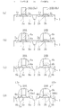
- FIGS. 10 (a) to 10 (d) are cross-sectional views of relevant steps showing a conventional method of manufacturing a semiconductor device in the order of steps.
- the Lvt region is a region where a P-type MIS transistor having a relatively low threshold voltage is formed
- the Hvt region is a region where a P-type MIS transistor having a relatively high threshold voltage is formed.
- an element isolation region 102 is formed on the silicon substrate 101.
- the region located in the Lvt region becomes the active region 101a in the Lvt region
- the region located in the Hvt region becomes the active region 101b in the Hvt region.
- an n-type channel region 103a having a first impurity concentration is formed above the active region 101a of the Lvt region, while a second impurity having a higher concentration than the first impurity concentration is formed above the active region 101b of the Hvt region.
- An n-type channel region 103b having an impurity concentration is formed.
- a high dielectric constant insulating film 104 and a metal film 105 are sequentially formed on the silicon substrate 101.
- a polysilicon film 111 is formed on the metal film 105.
- the Lvt region polysilicon film 111, the metal film 105, and the high dielectric constant insulating film 104 are sequentially patterned to form a high dielectric constant on the active region 101a in the Lvt region.
- a gate insulating film 104a made of an insulating film 104 and a gate electrode 120A made of a metal film 105a and a polysilicon film 111a are sequentially formed, and the polysilicon film 111, the metal film 105, and the high dielectric constant insulating film 104 in the Hvt region are formed.
- the gate insulating film 104b made of the high dielectric constant insulating film 104 and the gate electrode 120B made of the metal film 105b and the polysilicon film 111b are sequentially formed on the active region 101b in the Hvt region. Thereafter, a shallow p-type source / drain region 107a is formed in the active region 101a, and a shallow p-type source / drain region 107b is formed in the active region 101b.
- sidewalls 108a are formed on the side surfaces of the gate electrode 120A, and sidewalls 108b are formed on the side surfaces of the gate electrode 120B.
- a deep p-type source / drain region 109a is formed in the active region 101a
- a deep p-type source / drain region 109b is formed in the active region 101b.
- silicide films 110a1 and 110b1 are formed on the deep p-type source / drain regions 109a and 109
- silicide films 110a2 and 110b2 are formed on the polysilicon films 111a and 111b in the gate electrodes 120A and 120B.
- the impurity concentration of the channel region (see FIG. 10 (d): 103b) in the high threshold voltage MIS transistor is set to the channel region in the low threshold voltage MIS transistor. It is necessary to adjust it higher than the impurity concentration (see FIG. 10 (d): 103a). Thereby, the threshold voltage of the high threshold voltage system MIS transistor is controlled to be higher than the threshold voltage of the low threshold voltage system MIS transistor.
- the impurity concentration of the channel region in the high threshold voltage MIS transistor is relatively high, when the semiconductor device operates, the carriers collide with the conductive impurities contained in the channel region and scatter, resulting in a high threshold voltage.
- the MIS transistor there is a problem that the carrier mobility is reduced and the driving force is reduced.
- the impurity concentration of the channel region of the Lvt region and the channel region of the Hvt region can be uniformly reduced.
- the impurity concentration of the channel region of the Hvt region is set to the channel of the Lvt region.
- the method of adjusting the impurity concentration of the channel region is adopted as a method for controlling the threshold voltages of the MIS transistors having the same conductivity type, the driving capability of the high threshold voltage MIS transistor is lowered. The performance of the threshold voltage MIS transistor cannot be improved.
- the method of adjusting the Hf concentration of the gate insulating film it is very difficult to control the threshold voltage of the low and high threshold voltage MIS transistors. It cannot be realized with high accuracy. That is, no matter which method is used, MIS transistors having different threshold voltages cannot be realized with high accuracy and high performance.
- an object of the present invention is to realize MIS transistors having different threshold voltages with high accuracy and high performance in a semiconductor device including MIS transistors having the same conductivity type.
- a first semiconductor device includes a first MIS transistor and a second MIS transistor having a threshold voltage higher than that of the first MIS transistor.
- the first MIS transistor includes a first channel region formed in the first active region in the semiconductor substrate and a high dielectric constant insulation formed on the first channel region in the first active region.
- a first gate insulating film made of a film; a first conductive portion provided on and in contact with the first gate insulating film; and a second conductive portion formed on the first conductive portion.
- a second MIS transistor formed in a second active region of the semiconductor substrate, having a second channel region having the same conductivity type as the first channel region, and a second active region
- a second gate insulating film made of a high dielectric constant insulating film formed on the second channel region; a third conductive portion provided in contact with the second gate insulating film; and a third conductive portion
- a second gate electrode having a fourth conductive portion formed thereon, the third conductive portion being thinner than the first conductive portion and the same as the first conductive portion It consists of a composition material.
- the film thickness of the third conductive portion on which the fourth conductive portion is formed is the thickness of the first conductive portion on which the second conductive portion is formed.
- the threshold voltage of the second MIS transistor having the second gate electrode made up of the third conductive portion and the fourth conductive portion is reduced between the first conductive portion and the second conductive portion. It is controlled to be higher than the threshold voltage of the first MIS transistor having the first gate electrode formed of the conductive portion.
- the impurity concentration of the second channel region is not necessary to make the impurity concentration of the second channel region sufficiently higher than the impurity concentration of the first channel region as in the prior art, and the impurity concentration of the second channel region is reduced to that of the first channel region.
- the impurity concentration can be the same (or only slightly higher than the impurity concentration of the first channel region). Therefore, during operation of the semiconductor device, carriers can be prevented from colliding with the conductive impurities contained in the second channel region and scattered, so that in the second MIS transistor, leakage current can be reduced, and Thus, a high driving force can be achieved.
- the first and second MIS transistors are used instead of the conventional method of adjusting the Hf concentration of the gate insulating film constituting the MIS transistor. Since the method of adjusting the film thickness of the first and third conductive portions provided in contact with the first and second gate insulating films is adopted, the threshold value of the first and second MIS transistors is adopted. The voltage can be controlled easily and with high accuracy.
- the semiconductor device including the first and second MIS transistors having the same conductivity type the first and second MIS transistors having different threshold voltages can be improved in performance.
- the first conductive portion and the third conductive portion are made of metal or a metal compound, and the second conductive portion and the fourth conductive portion are made of silicon. .
- the second MIS transistor having the second gate insulating film and the second gate electrode is the first MIS having the first gate insulating film and the first gate electrode. It is preferable to have an effective work function close to that of silicon compared to a transistor.
- the first MIS transistor and the second MIS transistor are P-type MIS transistors, and the first conductive portion and the third conductive portion are 4.7 eV or more and 5 It is preferable to have a work function of .15 eV or less.
- the first MIS transistor and the second MIS transistor are P-type MIS transistors, and the first conductive portion and the third conductive portion are a titanium nitride film and a tantalum nitride.
- a film or a tantalum carbide film is preferable.
- the first MIS transistor and the second MIS transistor are P-type MIS transistors, and the first conductive portion and the third conductive portion are made of a titanium nitride film,
- the film thickness of the first conductive part is preferably 20 nm or more, and the film thickness of the third conductive part is preferably 15 nm or less.
- the first MIS transistor and the second MIS transistor are N-type MIS transistors, and the first conductive portion and the third conductive portion are 4.05 eV or more and 4 It preferably has a work function of .5 eV or less.
- the second channel region preferably has the same impurity concentration as the first channel region.
- the second gate insulating film has the same thickness as the first gate insulating film, and the fourth conductive portion has the same thickness as the second conductive portion. It is preferable to have.
- the thickness of the first gate electrode is preferably larger than the thickness of the second gate electrode.
- a second semiconductor device includes a first MIS transistor and a second MIS transistor having a threshold voltage higher than that of the first MIS transistor.
- the first MIS transistor includes a first channel region formed in the first active region in the semiconductor substrate and a high dielectric constant insulation formed on the first channel region in the first active region.
- the first conductive portion and the second conductive portion are made of materials having different compositions, so that the second gate electrode having the second conductive portion is provided.
- the threshold voltage of the second MIS transistor is controlled to be higher than the threshold voltage of the first MIS transistor including the first gate electrode having the first conductive portion.
- the impurity concentration of the second channel region is not necessary to make the impurity concentration of the second channel region sufficiently higher than the impurity concentration of the first channel region as in the prior art, and the impurity concentration of the second channel region is reduced to that of the first channel region.
- the impurity concentration can be the same (or only slightly higher than the impurity concentration of the first channel region). Therefore, during operation of the semiconductor device, carriers can be prevented from colliding with the conductive impurities contained in the second channel region and scattered, so that in the second MIS transistor, leakage current can be reduced, and Thus, a high driving force can be achieved.
- the first and second MIS transistors are used instead of the conventional method of adjusting the Hf concentration of the gate insulating film constituting the MIS transistor. Since the method of adjusting the conductive material of the first and second conductive portions provided in contact with the first and second gate insulating films is adopted, the threshold value of the first and second MIS transistors is adopted. The voltage can be controlled easily and with high accuracy.
- the semiconductor device including the first and second MIS transistors having the same conductivity type the first and second MIS transistors having different threshold voltages can be improved in performance.
- the second conductive portion has a work function closer to the silicon midgap work function than the first conductive portion.
- the first gate electrode is composed only of the first conductive portion
- the second gate electrode is composed only of the second conductive portion
- the first gate electrode has a third conductive portion formed on the first conductive portion, and the second gate electrode is on the second conductive portion. It is preferable to have the 4th electroconductive part formed in this.
- the first gate electrode is a fifth conductive portion made of the same conductive material as the second conductive portion between the first conductive portion and the third conductive portion. It is preferable to have.
- the second gate electrode includes a fifth conductive portion made of the same conductive material as the first conductive portion between the second conductive portion and the fourth conductive portion. It is preferable to have.
- the third conductive portion and the fourth conductive portion are made of silicon.
- the first conductive portion is made of the first metal or the first metal compound
- the second conductive portion is made of the second metal or the second metal compound. It is preferable.
- the first MIS transistor and the second MIS transistor are P-type MIS transistors
- the first conductive portion is a titanium nitride film
- the second conductive portion is A molybdenum nitride film or a tantalum nitride film is preferable.
- the second channel region preferably has the same impurity concentration as the first channel region.
- a first method of manufacturing a semiconductor device includes a first MIS transistor having a first gate electrode and a first threshold voltage higher than that of the first MIS transistor.
- a second gate insulating film made of a high dielectric constant insulating film on the second active region and forming a third conductive portion provided in contact with the second gate insulating film; And (d) forming a second gate electrode having a fourth conductive portion provided on the third conductive portion, wherein the third conductive portion is thinner than the first conductive portion. It has a film thickness and is made of the same composition material as that of the first conductive portion.
- the film thickness of the third conductive portion on which the fourth conductive portion is formed is the thickness of the third conductive portion on which the fourth conductive portion is formed.
- the effective work function of the second MIS transistor having the second gate electrode composed of the third conductive portion and the fourth conductive portion is changed to the first conductive portion.
- the effective work function of the second MIS transistor is changed to be closer to the mid gap than the effective work function of the first MIS transistor having the first gate electrode composed of the first and second conductive portions.
- the effective work function can be made closer to the “midgap work function of silicon”.
- the step (d) includes a step (d1) of forming a first metal film in contact with the high dielectric constant insulating film on the first active region, and a step ( a step (d2) of forming a first metal film and a second metal film in contact with the high dielectric constant insulating film on the second active region after d1), and a second metal after (d2)
- a silicon film, a second metal film, a first metal film, and a high dielectric constant insulating film on the first active region are formed.
- Patterning is performed to form a first gate insulating film made of a high dielectric constant insulating film, a first conductive part made of a first metal film and a second metal film, and a second conductive part made of a silicon film. And patterning the silicon film, the second metal film, and the high dielectric constant insulating film on the second active region.
- the step (d) includes a step (d1) of forming a metal film in contact with the high dielectric constant insulating film, and a second active region after the step (d1). Etching the upper portion of the upper metal film to form a metal thin film portion having a thickness smaller than that of the metal film, and after the step (d2), a silicon film is formed on the metal film and the metal thin film portion. After the forming step (d3) and the step (d3), the silicon gate, the metal film, and the high dielectric constant insulating film on the first active region are patterned to form a first gate made of the high dielectric constant insulating film.
- the insulating film, the first conductive portion made of a metal film, and the second conductive portion made of a silicon film are formed, and the silicon film, the metal thin film portion, and the high dielectric constant insulating film on the second active region are patterned.
- a second method of manufacturing a semiconductor device includes a first MIS transistor having a first gate electrode and a first threshold voltage higher than that of the first MIS transistor.
- first gate electrode having a first conductive portion provided on and in contact with the first gate insulating film, and forming a high dielectric constant insulating material on the second active region
- second gate insulating film made of a film
- second gate electrode having a second conductive portion provided in contact with the second gate insulating film (d).
- the second conductive portion is made of a composition material different from that of the first conductive portion.
- the first conductive portion and the second conductive portion are made of materials having different compositions, so that the work function of the second conductive portion is reduced to the first.
- the effective work function of the second MIS transistor having the second gate electrode having the second conductive portion is set to a work function close to the “silicon midgap work function” compared to the work function of the conductive portion of Compared to the effective work function of the first MIS transistor including the first gate electrode having the first conductive portion, the effective work function can be made closer to the “silicon mid-gap work function”.
- the step (d) includes a step (d1) of forming a first metal film in contact with the high dielectric constant insulating film on the first active region, and a second step. Forming a second metal film in contact with the high dielectric constant insulating film on the active region of the first active film after the step (d2) and the steps (d1) and (d2) And patterning the high dielectric constant insulating film to form a first gate insulating film made of the high dielectric constant insulating film and a first conductive portion made of the first metal film, and on the second active region Patterning the second metal film and the high dielectric constant insulating film to form a second gate insulating film made of the high dielectric constant insulating film and a second conductive part made of the second metal film ( d3).
- the step (d) includes a step (d1) of forming a first metal film in contact with the high dielectric constant insulating film on the first active region, and a second step. After the step (d2) of forming a second metal film in contact with the high dielectric constant insulating film on the active region, and after the steps (d1) and (d2), the first metal film and the second metal film After the step (d3) of forming a silicon film thereon and the step (d3), the silicon film, the first metal film, and the high dielectric constant insulating film on the first active region are patterned to obtain a high dielectric constant.
- Over gate insulating film preferably includes the second conductive portion made of the second metal film, and a step (d4) forming a fourth conductive portion made of a silicon film.
- the step (d) includes a step (d1) of forming a first metal film in contact with the high dielectric constant insulating film on the first active region, and a step ( After d1), a step (d2) of forming a first metal film and a second metal film in contact with the high dielectric constant insulating film on the second active region, and after the step (d2), the second metal film is formed.
- Forming a silicon film on the metal film (d3), and after the step (d3), the silicon film on the first active region, the second metal film, the first metal film, and the high dielectric constant insulating film The first gate insulating film made of a high dielectric constant insulating film, the first conductive part made of the first metal film, the fifth conductive part made of the second metal film, and the silicon film Forming a third conductive portion, a silicon film on the second active region, a second metal film, and a high dielectric constant isolation; Patterning the film to form a second gate insulating film made of a high dielectric constant insulating film, a second conductive part made of a second metal film, and a fourth conductive part made of a silicon film (d4) are preferably included.
- the film thickness of the conductive portion (or the conductive portion of the conductive portion) provided in contact with the first and second gate insulating films constituting the first and second MIS transistors By adjusting the conductive material, the effective work function of the second MIS transistor is controlled to be higher than the effective work function of the first MIS transistor. Therefore, in the semiconductor device having the first and second MIS transistors having the same conductivity type, the first and second MIS transistors having different threshold voltages can be realized with high accuracy and high performance.
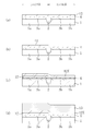
- FIGS. 1A to 1D are cross-sectional views of relevant steps showing a method of manufacturing a semiconductor device according to the first embodiment of the present invention in the order of steps.
- 2 (a) to 2 (d) are cross-sectional views of relevant steps showing the semiconductor device manufacturing method according to the first embodiment of the present invention in the order of steps.
- FIGS. 3A to 3D are cross-sectional views of relevant steps showing a method of manufacturing a semiconductor device according to the second embodiment of the present invention in the order of steps.
- FIGS. 4A to 4D are cross-sectional views of relevant steps showing a method of manufacturing a semiconductor device according to the second embodiment of the present invention in the order of steps.
- FIGS. 1A to 1D are cross-sectional views of relevant steps showing a method of manufacturing a semiconductor device according to the first embodiment of the present invention in the order of steps.
- 2 (a) to 2 (d) are cross-sectional views of relevant steps showing the semiconductor device manufacturing method according to the first embodiment of the present invention in the order of
- FIGS. 5A to 5D are cross-sectional views of relevant parts showing a method of manufacturing a semiconductor device according to the third embodiment of the present invention in the order of steps.
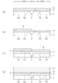
- FIG. 6 is a diagram showing the relationship between the effective work function of the P-type MIS transistor and the thickness of the TiN film.
- FIGS. 7A to 7D are cross-sectional views of relevant parts showing a method of manufacturing a semiconductor device according to the fourth embodiment of the present invention in the order of steps.
- FIGS. 8A to 8D are cross-sectional views of relevant steps showing a semiconductor device manufacturing method according to the fourth embodiment of the present invention in the order of steps.
- 9A to 9D are cross-sectional views of relevant steps showing a method of manufacturing a semiconductor device according to a modification of the fourth embodiment of the present invention in the order of steps.
- 10 (a) to 10 (d) are cross-sectional views of relevant steps showing a conventional method of manufacturing a semiconductor device in the order of steps.
- the word “midgap work function of silicon” means an intermediate value of the bandgap energy of silicon. For example, it is an intermediate value between the work function (about 4.05 eV) of silicon doped with negative charge (N-type silicon) and the work function (about 5.15 eV) of silicon doped with positive charge (P-type silicon). It means about 4.6 eV.
- band edge means the end value of the band gap energy of silicon.
- N-type MIS transistor it means about 4.05 eV which is the work function of silicon doped with negative charge (N-type silicon), and in the case of a P-type MIS transistor, silicon doped with positive charge. It means about 5.15 eV which is the work function of (P-type silicon).
- the terms “near the gap” and “near the band edge” mean that in the case of an N-type MIS transistor, for example, a first work function (or effective work function) of 4.3 eV and a second work function of 4.5 eV. (Or effective work function), the first work function (or effective work function) is “near the band edge” and the second work function (or effective work function) is “middle gap”. means.
- the first work function is compared with the second work function (or effective work function) of 4.9 eV
- the first work function is compared. This means that the function (or effective work function) is “close to the mid gap” and the second work function (or effective work function) is “close to the band edge”.
- a work function (or effective work function) close to the silicon mid gap work function (that is, about 4.6 eV as shown in the above 1) is “mid gap”.
- the work function (or effective work function) close to the band edge ie, N-type MIS transistor: about 4.05 eV, P-type MIS transistor: about 5.15 eV) as shown in the above 2) is “band”. It means “close to the edge”.
- work function means a physical property value indicating a difference between a vacuum level and an energy level of a metal (or metal compound).
- the term “effective work function” means a work function that effectively acts to determine the threshold voltage of the MIS transistor.
- the “effective work function” of the MIS transistor differs from the physical work function of the metal (or metal compound) constituting the MIS transistor due to various factors in the MIS transistor.
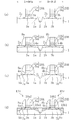
- FIGS. 1A to 1D and FIGS. 2A to 2D are cross-sectional views of relevant parts showing a method of manufacturing a semiconductor device according to the first embodiment of the present invention in order of steps.
- the Lvt region is a region where a P-type MIS transistor having a relatively low threshold voltage (hereinafter referred to as “low threshold transistor”) is formed, and the Hvt region has a relatively high threshold voltage.
- low threshold transistor a P-type MIS transistor having a relatively low threshold voltage
- high threshold transistor a P-type MIS transistor
- a one-conductivity type substrate having a semiconductor region such as a silicon region hereinafter referred to as “semiconductor substrate”.
- An element isolation region 2 in which an insulating film is buried in a trench is selectively formed on the upper portion of 1.
- an n-type well and an n-type punch-through stopper are formed by ion-implanting n-type impurities into the semiconductor substrate 1.
- the n-type well implantation conditions are such that the implanted ion species is P (phosphorus), the implantation energy is 400 keV, the implantation dose amount is 1 ⁇ 10 13 cm ⁇ 2 , and the n-type punch-through stopper implantation condition is The implanted ion species is P (phosphorus), the implantation energy is 200 keV, and the implantation dose is 1 ⁇ 10 13 cm ⁇ 2 .
- an n-type impurity is ion-implanted into the semiconductor substrate 1 to form an n-type channel region 3a above the first active region 1a and an n-type channel region above the second active region 1b.
- 3b is formed.
- the implantation conditions of the n-type channel regions 3a and 3b are as follows: the implanted ion species is As (arsenic), the implantation energy is 100 keV, the implantation dose is 2 ⁇ 10 12 cm ⁇ 2 , and the n-type channel region 3a The n-type channel region 3b is formed with substantially the same impurity concentration profile.
- a buffer insulating film (not shown) made of, for example, a silicon oxide film having a thickness of 0.5 nm on the semiconductor substrate 1, for example, a film is formed on the buffer insulating film.
- the buffer insulating film is formed between the semiconductor substrate 1 and the high dielectric constant insulating film 4.
- the “high dielectric constant insulating film 4” appearing in the following description is the buffer insulating film on the lower surface. A formed film.
- the first metal film 5 has a work function (eg, 4.9 eV) of 4.70 eV or more and 5.15 eV or less, and a second metal film described later (FIG. 1 (c): 6
- a film made of a metal or a metal compound having a work function closer to the band edge than the work function of (see) is desirable.
- a resist pattern (not shown) that covers the Lvt region and opens the Hvt region is formed on the first metal film 5, and then the resist pattern is used as a mask.
- the first metal film 5 in the Hvt region is etched to remove the first metal film 5 on the second active region 1b, and then the resist pattern is removed. Thereby, the first metal film 5 can be selectively left on the first active region 1a. In this way, the first metal film 5 in contact with the high dielectric constant insulating film 4 on the first active region 1a is formed.
- a second metal film 6 made of, for example, a 100 nm-thick molybdenum nitride film (MoN film) is deposited on the entire surface of the semiconductor substrate 1 by, eg, CVD.
- the second metal film 6 has a work function (for example, 4.7 eV) of 4.6 eV or more and 5.05 eV or less, and is closer to the mid gap than the work function of the first metal film 5.
- a film made of a metal or metal compound having a work function is desirable.
- a tantalum nitride film (TaN film) may be used instead of the MoN film.
- the second metal film 6 is polished and removed by, for example, a chemical mechanical polishing (CMP) method until the upper surface of the first metal film 5 is exposed. A region of the second metal film 6 located above the upper surface of the first metal film 5 is removed. As a result, the second metal film 6 remains on the second active region 1b. Then, the upper surface of the second metal film 6 is planarized so that its height is the same as the upper surface height of the first metal film 5. In other words, the first metal film 5 and the second metal film 6 are formed with substantially the same film thickness. In this way, the second metal film 6 in contact with the high dielectric constant insulating film 4 on the second active region 1b is formed.
- CMP chemical mechanical polishing
- a resist pattern (not shown) having a gate pattern shape is formed on the first metal film 5 and the second metal film 6 by, for example, photolithography.
- the first metal film 5 and the high dielectric constant insulating film 4 in the Lvt region are sequentially patterned by dry etching using the resist pattern as a mask, and the high dielectric constant insulating film is formed on the first active region 1a.
- the first gate insulating film 4a made of 4 and the first conductive portion 5a made of the first metal film 5 are sequentially formed.
- the second metal film 6 and the high dielectric constant insulating film 4 in the Hvt region are sequentially patterned, and the second gate insulating film 4b made of the high dielectric constant insulating film 4 is formed on the second active region 1b.
- the 2nd electroconductive part 6b which consists of a 2nd metal film 6 is formed in order.
- 20A is formed in sequence, and a second gate insulating film 4b and a second conductive portion 6b provided on and in contact with the second gate insulating film 4b are provided on the second active region 1b.
- Gate electrodes 20B are sequentially formed.
- p-type impurities are ion-implanted into the first active region 1a using the first gate electrode 20A as a mask, and the second gate electrode is introduced into the second active region 1b.
- a p-type source / drain region (LDD region or extension) having a relatively shallow junction depth is formed laterally below the first gate electrode 20A in the first active region 1a.
- Region) 7a is formed in a self-aligned manner, and a p-type source / drain region (LDD region or extension region) 7b having a relatively shallow junction depth below the side of the second gate electrode 20B in the second active region 1b.
- the implantation conditions for the shallow p-type source / drain regions 7a and 7b are that the implanted ion species is B (boron), the implantation energy is 0.5 keV, and the implantation dose is 5 ⁇ 10 14 cm ⁇ 2 .
- the sidewall 8a is formed on the side surface of the first gate electrode 20A, and the sidewall 8b is formed on the side surface of the second gate electrode 20B.
- p-type impurities are ion-implanted into the first active region 1a using the first gate electrode 20A and the sidewall 8a as a mask, and the second active region 1b.
- a p-type impurity is ion-implanted using the second gate electrode 20B and the sidewall 8b as a mask.
- a spike RTA (Rapid Thermal Annealing) process is performed on the semiconductor substrate 1 at 1050 ° C., for example, and a shallow p-type source / drain region 7a is bonded to the outside of the sidewall 8a in the first active region 1a.
- a p-type source / drain region 9a having a junction depth deeper than the depth and having a relatively deep junction depth is formed in a self-aligned manner, and is shallow on the outer side of the sidewall 8b in the second active region 1b.
- a p-type source / drain region 9b having a junction depth deeper than that of the p-type source / drain region 7b and having a relatively deep junction depth is formed in a self-aligned manner.
- the implantation conditions for the deep p-type source / drain regions 9a and 9b are that the implanted ion species is B (boron), the implantation energy is 2.0 keV, and the implantation dose is 3 ⁇ 10 15 cm ⁇ 2 .
- a silicide metal film (not shown) made of a nickel film (Ni film) having a thickness of 10 nm, for example, is deposited on the entire surface of the semiconductor substrate 1 by sputtering.
- the first RTA treatment is performed on the semiconductor substrate 1 in, for example, a nitrogen atmosphere at 320 ° C. to react each silicon in the deep p-type source / drain regions 9a and 9b with nickel of the metal film for silicide.
- the semiconductor substrate 1 is immersed in an etching solution composed of a mixed solution of sulfuric acid and hydrogen peroxide solution, whereby the element isolation region 2, the first conductive portion 5a in the first gate electrode 20A, and the second gate.
- the unreacted silicide metal film remaining on the second conductive portion 6b and the side walls 8a and 8b in the electrode 20B is removed.
- the second RTA process is performed on the semiconductor substrate 1 at a temperature (for example, 550 ° C.) higher than the temperature in the first RTA process.
- a silicide film 10a1 made of a nickel silicide film (NiSi film) is formed on the deep p-type source / drain region 9a in the Lvt region, and a nickel silicide film (on the upper side of the deep p-type source / drain region 9b in the Hvt region).
- a silicide film 10b1 made of a NiSi film is formed.
- the semiconductor device according to the present embodiment that is, the low threshold transistor LTr having the first gate electrode 20A composed of the first conductive portion 5a having the work function close to the band edge, and the first conductive A semiconductor device including the high threshold transistor HTr having the second gate electrode 20B made of the second conductive portion 6b having a composition different from that of the portion 5a and having a work function close to the midgap can be manufactured.
- an element isolation region 2 in which an insulating film is embedded in a trench is formed so as to partition the first active region 1a and the second active region 1b.
- the semiconductor device includes a low threshold transistor LTr provided in the first active region 1a and a high threshold transistor MTr provided in the second active region 1b.
- the low threshold transistor LTr includes an n-type channel region 3a formed in the first active region 1a, a first gate insulating film 4a made of a high dielectric constant insulating film formed on the n-type channel region 3a, A first gate electrode 20A formed of a first conductive portion 5a provided in contact with the first gate insulating film 4a; a sidewall 8a formed on a side surface of the first gate electrode 20A; A shallow p-type source / drain region 7a formed under the first gate electrode 20A in the active region 1a and a deep p-type source / drain formed under the sidewall 8a in the first active region 1a. A region 9a and a silicide film 10a1 formed on the deep p-type source / drain region 9a are provided.
- the high threshold transistor HTr includes an n-type channel region 3b formed in the second active region 1b and a second gate insulating film 4b made of a high dielectric constant insulating film formed on the n-type channel region 3b.
- a second gate electrode 20B comprising a second conductive portion 6b provided in contact with the second gate insulating film 4b, a sidewall 8b formed on the side surface of the second gate electrode 20B, A shallow p-type source / drain region 7b formed laterally below the second gate electrode 20B in the second active region 1b, and a deep p-type formed laterally below the sidewall 8b in the second active region 1b.
- a source / drain region 9b and a silicide film 10b1 formed on the deep p-type source / drain region 9b are provided.
- the first conductive portion 5a constituting the first gate electrode 20A of the low threshold transistor LTr is made of a TiN film and has a work function (for example, 4.9 eV) closer to the band edge.
- the second conductive portion 6b constituting the second gate electrode 20B of the high threshold transistor HTr is made of a MoN film and has a work function (for example, 4.7 eV) close to the mid gap.
- the first conductive portion 5a and the second conductive portion 6b are made of metal films having different compositions.
- the first conductive portion 5a has a work function closer to the “band edge (about 5.15 eV, see 2 above)” than the second conductive portion 6b.
- the second conductive portion 6b has a work function that is closer to the “midgap work function of silicon (about 4.6 eV, see 1) above” than the first conductive portion 5a. That is, the second conductive portion 6b has a work function lower than that of the first conductive portion 5a.
- the first gate insulating film 4a in contact with the first conductive portion 5a and the second gate insulating film 4b in contact with the second conductive portion 6b are formed in the same process and in the same structure. It consists of high dielectric constant insulating films having the same film thickness.
- n-type channel region 3a in the Lvt region and the n-type channel region 3b in the Hvt region are formed in the same process and in the same structure, and have the same impurity concentration. Note that “same film thickness” and “same impurity concentration” appearing in this specification mean that variations in manufacturing that occur in the same process are included.
- the shallow p-type source / drain regions 7a and 7b, the deep p-type source / drain regions 9a and 9b, and the sidewalls 8a and 8b are also formed in the same process and the same structure. However, if there is a difference in height between the first and second gate electrodes 20A and 20B, the side wall 8a formed on the side surface of the first gate electrode 20A and the side surface of the second gate electrode 20B will be described.
- the side wall 8b to be formed may be formed at different heights.
- the first conductive portion 5a and the second conductive portion 6b are made of metal films having different compositions, so that the work function of the second conductive portion 6b can be changed to that of the first conductive portion 5a.
- the effective work function of the high-threshold transistor HTr having the second gate electrode 20B formed of the second conductive portion 6b is set to a work function closer to the “silicon mid-gap work function” than the work function.
- the effective work function of the low threshold transistor LTr having the first gate electrode 20A formed of the portion 5a can be made lower. That is, the threshold voltage of the high threshold transistor MTr can be made higher than the threshold voltage of the low threshold transistor LTr.
- the impurity concentration of the n-type channel region (see FIG. 10 (d): 103b) in the Hvt region is set to be higher than the impurity concentration of the n-type channel region (see FIG. 10 (d): 103a) in the Lvt region.
- the impurity concentration of the n-type channel region 3b can be made the same as the impurity concentration of the n-type channel region 3a. Therefore, it is possible to suppress the carriers from colliding with the n-type impurity contained in the n-type channel region 3b and scattering during the operation of the semiconductor device, thereby reducing the leakage current in the high threshold transistor HTr, and High driving force can be achieved.
- the method for adjusting the Hf concentration of the gate insulating film constituting the low and high threshold transistors as in the conventional method is not used.
- the threshold voltage of the low and high threshold transistors can be easily and accurately controlled.
- MIS transistors having different threshold voltages can be realized with high accuracy and high performance.
- the first and second metal films 5 and 6 constituting the first and second conductive portions 5a and 6b having different work functions are used as the first and second metals having different compositions.
- the films 5 and 6 for example, the first metal film 5: TiN film and the second metal film 6: MoN film
- the present invention is not limited to this. .
- the first and second metal films constituting the first and second conductive parts even when the first and second metal films having different formation methods are used, even if the compositions are the same, Alternatively, even when the first and second metal films having the same composition and the same formation method are used, the first and second conductive parts having different work functions are realized. be able to.
- the n-type channel region 3a in the Lvt region and the n-type channel region 3b in the Hvt region are formed in the same process as shown in FIG.
- the present invention is not limited to this.
- n-type channel regions having slightly different impurity concentrations may be formed.
- the first and second gate electrodes including the first and second conductive portions having different work functions are used.
- n-type channel regions having slightly different impurity concentrations may be used.
- the impurity concentration of the n-type channel region of the Hvt region only needs to be slightly higher than the impurity concentration of the n-type channel region of the Lvt region. It is only necessary to provide a very small impurity concentration difference between the n-type channel region and the n-type channel region of the Hvt region. Therefore, a large impurity concentration difference is caused between the n-type channel region of the Lvt region (see FIG.
- the second activity is formed as shown in FIG. 1D.
- the present invention is not limited to this.
- the first metal film may be formed on the first active region.
- the second metal film 6 is formed by CMP as shown in FIG. 1D.
- the metal film 6 is removed by polishing, and then, as shown in FIG. 2A, the first metal film 5 and the second metal film 6 are patterned to form the first conductive film made of the first metal film 5.
- the case of forming the first gate electrode 20A having only the portion 5a and the second gate electrode 20B having only the second conductive portion 6b made of the second metal film 6 has been described as a specific example. However, the present invention is not limited to this. For example, similarly to the step shown in FIG.
- the first metal film and the second metal film are not polished and removed by CMP. Patterning the second metal film to form a first gate electrode having a conductive portion made of the first metal film and a conductive portion made of the second metal film formed on the conductive portion; A second gate electrode having only a conductive portion made of the metal film may be formed.
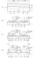
- FIGS. 4 (a) to (d) are cross-sectional views of relevant steps showing a method of manufacturing a semiconductor device according to the second embodiment of the present invention in the order of steps.
- FIG. 3 (a) to FIG. 4 (d) the same constituent elements as those of the first embodiment are denoted by the reference numerals shown in FIG. 1 (a) to FIG.
- the Lvt region is a region where a low threshold transistor is formed
- the Hvt region is a region where a high threshold transistor is formed.
- the first metal film 5 made of a 100 nm-thick TiN film in the first embodiment instead of the first metal film 5 made of a 100 nm-thick TiN film in the first embodiment, as shown in FIG. 3A, the first metal film made of a 20-nm thick TiN film is used. 1 metal film 5 is formed.
- the first metal film 5 in this embodiment preferably has a thickness of 20 nm or more, and has a work function (eg, 4.9 eV) of 4.70 eV or more and 5.15 eV or less.
- a film made of a metal or a metal compound having a work function closer to the band edge than the work function of a second metal film see FIG. 3 (c): 6) described later is desirable.
- the resist pattern is used as a mask.
- the first metal film 5 in the Hvt region is etched to remove the first metal film 5 on the second active region 1b, and then the resist pattern is removed. Thereby, the first metal film 5 can be selectively left on the first active region 1a. In this way, the first metal film 5 in contact with the high dielectric constant insulating film 4 on the first active region 1a is formed.
- a second metal film 6 made of, for example, a 20 nm-thick MoN film is deposited on the entire surface of the semiconductor substrate 1 by, eg, CVD.
- the same process as the process shown in FIG. 1 (c) in the first embodiment is performed.
- the film thickness (for example, 20 nm) of the second metal film 6 made of the MoN film in this embodiment is larger than the film thickness (for example, 100 nm) of the second metal film 6 made of the MoN film in the first embodiment. thin.
- the second metal film 6 in the present embodiment preferably has a thickness of 20 nm or more, and has a work function (for example, 4.7 eV) of 4.6 eV or more and 5.05 eV or less.
- a film made of a metal or a metal compound having a work function closer to the mid gap than the work function of the first metal film 5 is desirable.
- a TaN film may be used instead of the MoN film.
- a resist pattern (not shown) that opens the Lvt region and covers the Hvt region is formed on the second metal film 6, and then the resist pattern is used as a mask. Dry etching is performed on the second metal film 6 in the Lvt region to remove the second metal film 6 on the first metal film 5, and then the resist pattern is removed. Thereby, the second metal film 6 can be selectively left on the second active region 1b. In this way, the second metal film 6 in contact with the high dielectric constant insulating film 4 on the second active region 1b is formed.
- a polysilicon film having a film thickness of, for example, 100 nm is formed on the first metal film 5 and the second metal film 6, and then a p-type impurity is ion-implanted into the polysilicon film.
- a silicon film 11 made of a silicon film is formed.
- the implantation conditions of the silicon film 11 are that the implanted ion species is B (boron), the implantation energy is 3 keV, and the implantation dose is 1 ⁇ 10 15 cm ⁇ 2 .
- a resist pattern (not shown) having a gate pattern shape is formed on the silicon film 11 by, eg, photolithography. Thereafter, by using the resist pattern as a mask, the silicon film 11, the first metal film 5, and the high dielectric constant insulating film 4 in the Lvt region are sequentially patterned by dry etching, on the first active region 1a.
- a first gate insulating film 4 a made of the high dielectric constant insulating film 4, a first conductive part 5 a made of the first metal film 5, and a third conductive part 11 a made of the silicon film 11 are sequentially formed.
- the silicon film 11, the second metal film 6, and the high dielectric constant insulating film 4 in the Hvt region are sequentially patterned to form the second dielectric layer 4 made of the high dielectric constant insulating film 4 on the second active region 1b.
- a gate insulating film 4b, a second conductive portion 6b made of the second metal film 6, and a fourth conductive portion 11b made of the silicon film 11 are sequentially formed.
- first gate insulating film 4a and the first conductive part 5a provided on and in contact with the first gate insulating film 4a on the first active region 1a, and the first conductive part
- a first gate electrode 20A having a third conductive portion 11a formed on 5a is sequentially formed, and a second gate insulating film 4b and a second gate insulation are formed on the second active region 1b.
- a second gate electrode 20B having a second conductive portion 6b provided in contact with the film 4b and a fourth conductive portion 11b formed on the second conductive portion 6b is sequentially formed.
- the first gate electrode 20A side in the first active region 1a is used.
- a p-type source / drain region 7a having a relatively shallow junction depth is formed in a self-aligned manner, and a relatively shallow junction depth is formed laterally below the second gate electrode 20B in the second active region 1b.
- a p-type source / drain region 7b is formed in a self-aligning manner.
- a side surface of the first gate electrode 20A is formed using a method similar to the method of forming the sidewall in the step shown in FIG. 2B in the first embodiment.
- a sidewall 8a is formed thereon, and a sidewall 8b is formed on the side surface of the second gate electrode 20B.
- a p-type source / drain region 9a having a relatively deep junction depth is formed in the region 1a outside the sidewall 8a in a self-aligned manner, and the junction depth is formed outside the sidewall 8b in the second active region 1b.
- a relatively deep p-type source / drain region 9b is formed in a self-aligned manner.
- a silicide metal film (not shown) made of, for example, a 10 nm-thickness Ni film is deposited on the entire surface of the semiconductor substrate 1 by sputtering. Thereafter, for example, the first RTA process is performed on the semiconductor substrate 1 in a nitrogen atmosphere at 320 ° C., and each of the deep p-type source / drain regions 9a and 9b and the third and fourth conductive portions 11a and 11b. Silicon is reacted with nickel of the metal film for silicide.
- the unreacted metal for silicide remaining on the element isolation region 2 and the sidewalls 8a and 8b by immersing the semiconductor substrate 1 in an etching solution made of a mixed solution of sulfuric acid and hydrogen peroxide. Remove the membrane. Thereafter, the second RTA process is performed on the semiconductor substrate 1 at a temperature (for example, 550 ° C.) higher than the temperature in the first RTA process.
- a temperature for example, 550 ° C.
- silicide films 10a1 and 10b1 made of NiSi film are formed on the deep p-type source / drain regions 9a and 9b, and the third and fourth conductive portions 11a in the first and second gate electrodes 20A and 20B are formed.
- 11b silicide films 10a2 and 10b2 made of NiSi film are formed.
- the semiconductor device that is, the first conductive portion 5a having the work function (for example, 4.9 eV) closer to the band edge and the first conductive portion 11a.
- a low threshold transistor LTr having a gate electrode 20A, a second conductive portion 6b having a work function (for example, 4.7 eV) close to a mid gap, and a second gate electrode 20B having a fourth conductive portion 11b.
- a semiconductor device including the high threshold transistor HTr can be manufactured.
- the first and second gate electrodes 20A and 20B in this embodiment have a so-called MIPS (Metal Insert Poly-Silicon) electrode structure composed of a metal film and a polysilicon film formed thereon. is doing.
- MIPS Metal Insert Poly-Silicon
- the first gate electrode 20A of the low threshold transistor LTr has a first conductive part 5a made of the first metal film 5 and a third conductive part 11a made of the silicon film 11.
- the second gate electrode 20B of the high threshold transistor HTr has a second conductive portion 6b made of the second metal film 6 and a fourth conductive portion 11b made of the silicon film 11.
- the first conductive portion 5a provided in contact with the first gate insulating film 4a and the second conductive portion 6b provided in contact with the second gate insulating film 4b have different compositions from each other. It is composed of a film (first conductive portion 5a: TiN film, second conductive portion 6b: MoN film), and the second conductive portion 6b is “a silicon midgap work function” as compared to the first conductive portion 5a. Has a work function close to.
- the third conductive portion 11a formed on the first conductive portion 5a and the fourth conductive portion 11b formed on the second conductive portion 6b have the same film thickness (for example, 100 nm), and And made of a silicon film having the same composition. That is, the first conductive portion 5a and the second conductive portion 6b are formed thereon with third and fourth conductive portions 11a and 11b made of silicon films having the same film thickness and the same composition.
- the first gate insulating film 4a in contact with the first conductive portion 5a and the second gate insulating film 4b in contact with the second conductive portion 6b are formed in the same process and in the same structure. It consists of high dielectric constant insulating films having the same film thickness.
- n-type channel region 3a in the Lvt region and the n-type channel region 3b in the Hvt region are formed in the same process and in the same structure, and have the same impurity concentration.
- the shallow p-type source / drain regions 7a and 7b, the deep p-type source / drain regions 9a and 9b, and the sidewalls 8a and 8b are also formed in the same process and the same structure. However, if there is a difference in height between the first and second gate electrodes 20A and 20B, the side wall 8a formed on the side surface of the first gate electrode 20A and the side surface of the second gate electrode 20B will be described.
- the side wall 8b to be formed may be formed at different heights.
- the first conductive portion 5a and the second conductive portion 6b are made of metal films having different compositions, so that the work function of the second conductive portion 6b can be reduced by the first conductive portion 5a.
- the effective function of the high threshold transistor HTr having the second gate electrode 20B composed of the second conductive portion 6b and the fourth conductive portion 11b is set to a work function closer to the “silicon midgap work function” than the work function.
- the work function can be made lower than the effective work function of the low threshold transistor LTr having the first gate electrode 20A composed of the first conductive portion 5a and the third conductive portion 11a. That is, the threshold voltage of the high threshold transistor MTr can be made higher than the threshold voltage of the low threshold transistor LTr. Therefore, the low and high threshold transistors LTr and HTr having different threshold voltages can be realized with high accuracy.
- the first gate electrode 20A is formed by patterning with the silicon film 11 formed on the first metal film 5, and the second metal film 6 is formed. Since the second gate electrode 20B can be formed by patterning with the silicon film 11 formed thereon, the patterning accuracy of the first and second gate electrodes 20A and 20B can be greatly improved.
- the first and second gate electrodes 20A and 20B patterned with high accuracy can be realized.
- the first gate electrode 20A in the present embodiment includes a first conductive portion 5a having a relatively thin film thickness and a third conductive portion that is easier to pattern than the first conductive portion 5a formed thereon. 11a.
- the second gate electrode 20B in this embodiment includes a second conductive portion 6b having a relatively small thickness and a fourth conductive pattern that is easier to pattern than the second conductive portion 6b formed thereon. Part 11b.
- the case where the second metal film 6 on the first metal film 5 is removed by dry etching has been described as a specific example.
- the invention is not limited to this.
- the second metal film 6 on the first metal film 5 may be polished and removed by the CMP method.
- the second activity is formed as shown in FIG. 3D.
- the present invention is not limited to this.
- the first metal film may be formed on the first active region.
- FIGS. 5 (a) to 5 (d) are cross-sectional views of relevant parts showing a method of manufacturing a semiconductor device according to the third embodiment of the present invention in the order of steps.
- FIGS. 5A to 5D the same components as those in the first embodiment or the second embodiment described above are shown in FIGS. 1A to 2 in the first embodiment.
- the same reference numerals as those shown in d) or the same reference numerals as those shown in FIGS. 3A to 4D in the second embodiment are given, and redundant description is omitted.
- the Lvt region is a region where a low threshold transistor is formed
- the Hvt region is a region where a high threshold transistor is formed.
- the first metal film 5 and the second metal film 6 are removed.
- the first metal film 6 on the first metal film 5 is not removed and the first metal film 11 is removed.
- the second metal film 6 is left on the metal film 5 to form a silicon film 11 on the second metal film 6.
- a polysilicon film having a thickness of, for example, 100 nm is formed on the second metal film 6
- p-type impurities are ion-implanted into the polysilicon film.
- a silicon film 11 made of a p-type polysilicon film is formed.
- the implantation conditions for the silicon film 11 are the same implantation conditions as in the second embodiment.
- a resist pattern (not shown) having a gate pattern shape is formed on the silicon film 11 by, eg, photolithography. Thereafter, by using the resist pattern as a mask, the silicon film 11, the second metal film 6, the first metal film 5, and the high dielectric constant insulating film 4 in the Lvt region are sequentially patterned by dry etching to obtain the first On the active region 1 a, a first gate insulating film 4 a made of the high dielectric constant insulating film 4, a first conductive portion 5 a made of the first metal film 5, and a fifth conductive made of the second metal film 6. A third conductive portion 11a made up of the portion 6a and the silicon film 11 is sequentially formed.
- the silicon film 11, the second metal film 6, and the high dielectric constant insulating film 4 in the Hvt region are sequentially patterned to form the second dielectric layer 4 made of the high dielectric constant insulating film 4 on the second active region 1b.
- a gate insulating film 4b, a second conductive portion 6b made of the second metal film 6, and a fourth conductive portion 11b made of the silicon film 11 are sequentially formed.
- first gate insulating film 4a and the first conductive part 5a provided on and in contact with the first gate insulating film 4a on the first active region 1a, and the first conductive part
- a first gate electrode 20A having a fifth conductive portion 6a formed on 5a and a third conductive portion 11a formed on the fifth conductive portion 6a is sequentially formed, and a second active portion
- a second gate electrode 20B having a conductive portion 11b is sequentially formed.
- the first gate electrode 20A side in the first active region 1a is used.
- a p-type source / drain region 7a having a relatively shallow junction depth is formed in a self-aligned manner, and a relatively shallow junction depth is formed laterally below the second gate electrode 20B in the second active region 1b.
- a p-type source / drain region 7b is formed in a self-aligning manner.
- the side surface of the first gate electrode 20A is formed using a method similar to the method of forming the sidewall in the step shown in FIG. 2B in the first embodiment.
- a sidewall 8a is formed thereon, and a sidewall 8b is formed on the side surface of the second gate electrode 20B.
- the outer side of the sidewall 8a in the first active region 1a is formed.
- a p-type source / drain region 9a having a relatively deep junction depth is formed in a self-aligned manner, and a p-type source / drain region 9b having a relatively deep junction depth is formed outside the sidewall 8b in the second active region 1b. Are formed in a self-aligning manner.
- a deep p-type source / drain region 9a a method similar to the method for forming a silicide film in the step shown in FIG. 4D in the second embodiment is used.
- Silicide films 10a1 and 10b1 made of NiSi film are formed on the upper part of 9b, and silicide films made of NiSi film are formed on the third and fourth conductive portions 11a and 11b in the first and second gate electrodes 20A and 20B.
- 10a2 and 10b2 are formed.
- the semiconductor device that is, the first conductive portion 5a, the fifth conductive portion 6a, and the third conductive portion having a work function (for example, 4.9 eV) closer to the band edge.
- a low-threshold transistor LTr having a first gate electrode 20A formed of a portion 11a, a second conductive portion 6b having a work function (for example, 4.7 eV) near the mid gap, and a fourth conductive portion 11b.
- a semiconductor device including a high threshold transistor HTr having two gate electrodes 20B can be manufactured.
- the first and second gate electrodes 20A and 20B in this embodiment have a so-called MIPS electrode structure including the metal film and the polysilicon film formed thereon.
- the first gate electrode 20A of the low threshold transistor LTr has a first conductive portion 5a and a third conductive portion 11a as shown in FIG. 4D.
- the first conductive portion 5a, the fifth conductive portion 6a, and the third conductive portion 11a are provided.
- the first gate electrode 20A in the present embodiment is the same conductive material as the second conductive portion 6b constituting the second gate electrode 20B between the first conductive portion 5a and the third conductive portion 11a. And a fifth conductive portion 6a.
- a lower conductive portion (first conductive portion 5a, second conductive portion 6b) provided in contact with the gate insulating film and an upper conductive portion (fifth conductive portion formed on the lower conductive portion).
- the threshold voltage of the transistor is the upper conductive voltage. Not affected by the department.
- the first gate electrode 20A in the present embodiment has a configuration in which a fifth conductive portion 6a having a work function close to the mid gap is interposed between the first conductive portion 5a and the third conductive portion 11a.
- the threshold voltage of the low threshold transistor LTr having the first gate electrode 20A is the fifth conductive portion 6a. Not affected.
- the low threshold transistor LTr in this embodiment is a low threshold transistor LTr in the second embodiment (that is, a first configuration in which no conductive portion is interposed between the first conductive portion 5a and the third conductive portion 11a).
- the low threshold transistor LTr) having one gate electrode 20A has substantially the same threshold voltage.
- the second metal film 6 is left on the first metal film 5 without removing the second metal film 6 on the first metal film 5. . That is, since the second metal film on the first metal film is not removed as in the second embodiment (see FIG. 3D), the manufacturing method can be simplified.
- the second metal film 6 is formed on the semiconductor substrate 1. Thereafter, the case where the silicon film 11 is formed on the second metal film 6 has been described as a specific example, but the present invention is not limited to this.
- the first metal film may be formed on the semiconductor substrate, and then the silicon film may be formed on the first metal film.
- the gate electrode of the low threshold transistor has a conductive portion made of the first metal film and a conductive portion made of the silicon film, and the configuration thereof is the same as that of the first gate electrode 20A in the second embodiment. Same as the configuration.
- the gate electrode of the high threshold transistor has a conductive portion made of the second metal film, a conductive portion made of the first metal film, and a conductive portion made of the silicon film.
- the same conductive material as that of the first conductive portion 5a is provided between the second conductive portion 6b and the fourth conductive portion 11b in the second embodiment.
- the conductive portion (that is, the conductive portion having a work function near the band edge) is interposed.
- the second conductive portion 6b provided in contact with the second gate insulating film 4b constituting the high threshold transistor HTr has a sufficiently thick film thickness (for example, 20 nm), so that the second Even in the case of a high-threshold transistor having a gate electrode configured such that a conductive portion having a work function close to the band edge is interposed between the conductive portion 6b and the fourth conductive portion 11b, the conductive portion is not interposed.
- the threshold voltage is substantially the same as that of the high threshold transistor having the gate electrode of the configuration (that is, the high threshold transistor HTr in the second embodiment).
- the channel regions having different impurity concentrations between the low threshold transistor LTr and the high threshold transistor MTr (FIG. 10 (d): 103a, 103b) 2), or low and high threshold transistors LTr having different threshold voltages from each other by providing low and high threshold transistors LTr and HTr having different effective work functions. This is common in realizing the HTr.
- the first conductive portion 5a provided in contact with the first gate insulating film 4a constituting the low threshold transistor LTr and the second gate constituting the high threshold transistor HTr Since the second conductive portion 6b provided in contact with the insulating film 4b is made of metals or metal compounds having different compositions, the first and second conductive portions 5a and 6b having different work functions are provided. Thus, low and high threshold transistors LTr and HTr having different effective work functions are realized.
- a first conductive portion (see FIG. 8D: 12a described later) provided in contact with the first gate insulating film constituting the low threshold transistor, and the high threshold transistor Or a third conductive portion (see FIG. 8 (d): 12b described later) provided in contact with the second gate insulating film constituting the same metal and having a different film thickness, Second and fourth conductive parts made of a metal compound and having the same film thickness on the first and third conductive parts and made of silicon (see FIG. 8 (d): 13a and 13b described later) ) To realize low and high threshold transistors having different effective work functions.
- the effective work function of the transistor depends on the film thickness of the metal film.
- the metal film formed on the gate insulating film made of the high dielectric constant insulating film is the TiN film in the gate electrode constituting the P-type MIS transistor.
- the silicon film is a p-type polysilicon film having a film thickness of 100 nm will be described as a specific example with reference to FIG.
- FIG. 6 is a diagram showing the relationship between the effective work function of the P-type MIS transistor and the film thickness of the metal film.
- the horizontal axis in FIG. 6 indicates the thickness of the TiN film on the gate electrode
- the left vertical axis in FIG. 6 indicates the effective work function of the P-type MIS transistor
- the right vertical axis indicates the threshold voltage of the P-type MIS transistor.
- the effective work function of the P-type MIS transistor rapidly decreases according to the decrease in the thickness of the TiN film (in other words, shifts closer to the mid gap).
- the threshold voltage of the P-type MIS transistor rapidly increases.
- the thickness of the TiN film is 20 nm or more, the effective work function of the P-type MIS transistor gradually increases as the thickness of the TiN film increases, and the threshold voltage of the P-type MIS transistor gradually decreases.
- the effective work function of the P-type MIS transistor when the film thickness of the TiN film is 15 nm or less, the effective work function of the P-type MIS transistor is relatively high in film thickness, and as the film thickness of the TiN film decreases, the effective work function becomes closer to the mid gap. Effective work function.
- the thickness of the TiN film is 20 nm or more, the effective work function of the P-type MIS transistor is relatively low in film thickness dependency and remains an effective work function close to the band edge (that is, about 5.15 eV). is there.
- the effective work function of the P-type MIS transistor is about 4.85 eV
- the thickness of the TiN film is 10 nm (that is, 15 nm or less).
- the effective work function of the P-type MIS transistor is about 4.75 eV.
- the MIS transistor decreases as the thickness of the metal film decreases.
- the effective work function shifts continuously toward the midgap. This is because when the metal film is sufficiently thick, it is not greatly affected by the silicon film formed on the metal film, but when the metal film is thin, it is greatly influenced by the silicon film, and the MIS transistor. It is understood that the effective work function of shifts toward the midgap.
- the dependence on the effective work function is relatively low.
- a film thickness for example, a TiN film having a film thickness of 20 nm or more
- a conductive portion for example, a TiN film having a film thickness of 15 nm or less
- the effective work function of the high threshold transistor is made higher than that of the low threshold transistor.
- the relationship between the effective work function of the P-type MIS transistor shown in FIG. 6 and the film thickness of the metal film is established only in the case of the P-type MIS transistor having a gate electrode in which a 100 nm silicon film is formed on the metal film. This relationship is not always true, but is a relationship that always holds in a P-type MIS transistor having a gate electrode in which a silicon film having a thickness of a certain degree (for example, 50 nm) or more is formed on a metal film.
- the relationship between the effective work function of the P-type MIS transistor and the film thickness of the metal film shown in FIG. 6 is not a relationship that holds only in the case of the P-type MIS transistor, but also holds in the case of the N-type MIS transistor. It is. That is, in an N-type MIS transistor having a gate electrode in which a silicon film is formed on a metal film, the effective work function of the N-type MIS transistor continuously approaches the midgap as the thickness of the metal film decreases. shift.
- FIGS. 7A to 7D and FIGS. 8A to 8D are cross-sectional views of relevant steps showing a method of manufacturing a semiconductor device according to the fourth embodiment of the present invention in the order of steps.
- FIGS. 7A to 8D the same components as those in the first embodiment or the second embodiment described above are the same as those in FIG.
- the same reference numerals as those shown in 2 (d) or the symbols shown in FIG. 3 (a) to FIG. 4 (d) in the second embodiment are given, and redundant explanations are omitted.
- the Lvt region is a region where the low threshold transistor LTr is formed
- the Hvt region is a region where the high threshold transistor MTr is formed.
- a device isolation region 2 in which an insulating film is buried in a trench is selectively formed, for example, on the upper portion of the semiconductor substrate 1 by, for example, the STI method.
- the region located in the Lvt region among the regions surrounded by the element isolation region 2 in the semiconductor substrate 1 becomes the first active region 1a, while the region located in the Hvt region becomes the second active region 1b.
- an n-type well and an n-type punch-through stopper are formed by ion-implanting n-type impurities into the semiconductor substrate 1.
- an n-type impurity is ion-implanted into the semiconductor substrate 1 to form an n-type channel region 3a above the first active region 1a and an n-type channel region above the second active region 1b. 3b is formed.
- the implantation conditions for the n-type well, the n-type punch-through stopper, and the n-type channel regions 3a and 3b are the same as those in the first embodiment.
- a buffer insulating film (not shown) made of, for example, a silicon oxide film having a thickness of 0.5 nm on the semiconductor substrate 1, for example, a film is formed on the buffer insulating film.
- a high dielectric constant insulating film 4 made of a 4 nm thick HfSiON film is formed.
- the buffer insulating film is formed between the semiconductor substrate 1 and the high dielectric constant insulating film 4.
- the “high dielectric constant insulating film 4” appearing in the following description is the buffer insulating film on the lower surface. A formed film.
- a first metal film made of, for example, a 10 nm-thick titanium nitride film (TiN film) on the high dielectric constant insulating film 4 by, eg, CVD (herein, “metal film” is a film made of a metal or a metal compound) 12) is deposited.
- the first metal film 12 desirably has a work function (for example, 4.9 eV) of 4.7 eV or more and 5.15 eV or less.
- a tantalum nitride film (TaN film) or a tantalum carbide film (TaC film) may be used instead of the TiN film.
- TiN film titanium nitride film
- a polysilicon film having a film thickness of, for example, 100 nm is formed on the second metal film 12X, p-type impurities are ion-implanted into the polysilicon film.
- a silicon film 13 made of a p-type polysilicon film is formed.
- the implantation conditions for the silicon film 13 are the same as the implantation conditions for the silicon film 11 in the second embodiment.
- a resist pattern (not shown) having a gate pattern shape is formed on the silicon film 13 by, eg, photolithography. Thereafter, by using the resist pattern as a mask, the silicon film 13, the second metal film 12X, the first metal film 12, and the high dielectric constant insulating film 4 in the Lvt region are sequentially patterned by dry etching. From the first gate insulating film 4a made of the high dielectric constant insulating film 4, the first conductive portion 12a made of the first metal film 12A and the second metal film 12XA, and the silicon film 13 on the active region 1a Second conductive portions 13a are sequentially formed.
- the silicon film 13 in the Hvt region, the second metal film 12X, and the high dielectric constant insulating film 4 are sequentially patterned to form the second dielectric layer 4 made of the high dielectric constant insulating film 4 on the second active region 1b.
- a gate insulating film 4b, a third conductive portion 12b made of the second metal film 12XB, and a fourth conductive portion 13b made of the silicon film 13 are sequentially formed.
- the film thickness of the first conductive part 12a is 20 nm, which is the total film thickness of the first metal film 12A and the second metal film 12XA
- the film thickness of the third conductive part 12b is the second film thickness.
- the thickness of the metal film 12XB is 10 nm.
- first gate insulating film 4a the first conductive portion 12a provided on the first active region 1a in contact with the first gate insulating film 4a, and the first conductive portion
- a first gate electrode 20A having a second conductive portion 13a provided on 12a is sequentially formed, and a second gate insulating film 4b and a second gate insulation are formed on the second active region 1b.
- a second gate electrode 20B having a third conductive portion 12b provided in contact with the film 4b and a fourth conductive portion 13b provided on the third conductive portion 12b is sequentially formed.
- the first gate electrode 20A side in the first active region 1a is used.
- a p-type source / drain region 7a having a relatively shallow junction depth is formed in a self-aligned manner, and a relatively shallow junction depth is formed laterally below the second gate electrode 20B in the second active region 1b.
- a p-type source / drain region 7b is formed in a self-aligning manner.
- the side surface of the first gate electrode 20A is formed using a method similar to the method of forming the sidewall in the step shown in FIG. 2B in the first embodiment.
- a sidewall 8a is formed thereon, and a sidewall 8b is formed on the side surface of the second gate electrode 20B.
- a p-type source / drain region 9a having a relatively deep junction depth is formed in the region 1a outside the sidewall 8a in a self-aligned manner, and the junction depth is formed outside the sidewall 8b in the second active region 1b.
- a relatively deep p-type source / drain region 9b is formed in a self-aligned manner.
- a deep p-type source / drain region 9a a method similar to the method for forming a silicide film in the step shown in FIG. 4D in the second embodiment is used.
- Silicide films 10a1 and 10b1 made of NiSi film are formed on the top of 9b, and silicide films made of NiSi film are formed on the second and fourth conductive portions 13a and 13b in the first and second gate electrodes 20A and 20B.
- 10a2 and 10b2 are formed.
- the semiconductor device that is, the first conductive portion 12a having a film thickness (for example, 20 nm) at which an effective work function (for example, 4.85 eV) near the band edge is obtained, and the first The low threshold transistor LTr having the first gate electrode 20A composed of the two conductive portions 13a and the effective work function (for example, 4.75 eV) close to the mid gap with the same composition as the first conductive portion 12a are obtained.
- a semiconductor device including the third conductive portion 12b having a desired film thickness (for example, 10 nm) and the high threshold transistor HTr having the second gate electrode 20B made of the fourth conductive portion 13b can be manufactured.
- an element isolation region 2 in which an insulating film is embedded in a trench is formed so as to partition the first active region 1a and the second active region 1b.
- the semiconductor device includes a low threshold transistor LTr provided in the first active region 1a and a high threshold transistor MTr provided in the second active region 1b.
- the low threshold transistor LTr includes an n-type channel region 3a formed in the first active region 1a, a first gate insulating film 4a made of a high dielectric constant insulating film formed on the n-type channel region 3a, A first gate electrode 20A having a first conductive portion 12a provided in contact with the first gate insulating film 4a and a second conductive portion 13a formed on the first conductive portion 12a; A sidewall 8a formed on the side surface of the first gate electrode 20A, a shallow p-type source / drain region 7a formed laterally below the first gate electrode 20A in the first active region 1a, and a first A deep p-type source / drain region 9a formed on the outer side of the sidewall 8a in the active region 1a, a silicide film 10a1 formed on the deep p-type source / drain region 9a, and a first gate And a silicide film 10a2 formed in an upper portion of the pole 20A.
- the high threshold transistor HTr includes an n-type channel region 3b formed in the second active region 1b and a second gate insulating film 4b made of a high dielectric constant insulating film formed on the n-type channel region 3b.
- a second gate electrode 20B having a third conductive portion 12b provided in contact with the second gate insulating film 4b and a fourth conductive portion 13b formed on the third conductive portion 12b; A sidewall 8b formed on the side surface of the second gate electrode 20B, a shallow p-type source / drain region 7b formed laterally below the second gate electrode 20B in the second active region 1b, A deep p-type source / drain region 9b formed on the outer side of the sidewall 8b in the second active region 1b, a silicide film 10b1 formed on the deep p-type source / drain region 9b, and a second And a silicide film 10b2 formed in an upper portion of the over gate electrode 20B.
- the third conductive portion 12b constituting the second gate electrode 20B of the high threshold transistor LTr is thinner than the first conductive portion 12a constituting the first gate electrode 20A of the low threshold transistor LTr, and
- the first conductive portion 12a is made of a metal or a metal compound having the same composition, and has the same work function as the first conductive portion 12a.
- the first conductive portion 12a and the third conductive portion 12b are formed thereon with second and fourth conductive portions 13a and 13b made of silicon films having the same film thickness.
- the first conductive portion 12a is made of a TiN film having a thickness of 20 nm (that is, 20 nm or more), and the third conductive portion 12b is made of a TiN film having a thickness of 10 nm (that is, 15 nm or less).
- the second and fourth conductive portions 13a and 13b are made of a p-type polysilicon film having a thickness of 100 nm.
- a low threshold transistor LTr having an effective work function of about 4.85 eV is realized, and the threshold voltage of the low threshold transistor LTr is set to about 0.30 V, while an effective value of about 4.75 eV is achieved.
- the high threshold transistor HTr having a work function can be realized, and the threshold voltage of the high threshold transistor HTr can be set to about 0.40V.
- the film thickness of the first conductive portion 12a As described above, as the film thickness of the first conductive portion 12a, a film thickness that exhibits a relatively low dependence on the effective work function is adopted, while the film thickness of the third conductive portion 12b is set to the effective work function.
- a film thickness that shows a relatively high dependence on the effective work function of the high threshold transistor HTr having the second gate electrode 20B composed of the third conductive portion 12b and the fourth conductive portion 13b By adopting a film thickness that shows a relatively high dependence on the effective work function of the high threshold transistor HTr having the second gate electrode 20B composed of the third conductive portion 12b and the fourth conductive portion 13b.
- the effective work function of the low threshold transistor LTr having the first gate electrode 20A composed of the first conductive portion 12a and the second conductive portion 13a can be shifted closer to the mid gap.
- the high-threshold transistor HTr has an effective work function that is closer to “the mid-gap work function of silicon (about 4.6 eV, see 1) above” than the low-threshold transistor LTr.
- the low threshold transistor LTr has an effective work function closer to “band edge (about 5.15 eV, see 2 above)” than the high threshold transistor MTr. That is, the low threshold transistor LTr has a higher effective work function than the high threshold transistor HTr.
- the first gate insulating film 4a in contact with the first conductive portion 12a and the second gate insulating film 4b in contact with the third conductive portion 12b are formed in the same process and in the same structure. It consists of high dielectric constant insulating films having the same film thickness.
- the second conductive portion 13a formed on the first conductive portion 12a and the fourth conductive portion 13b formed on the third conductive portion 12b are made of silicon films having the same film thickness. .
- the first gate electrode 20A composed of the first conductive portion 12a and the second conductive portion 13a has a thickness smaller than that of the first conductive portion 12a, the third conductive portion 12b, and the second conductive portion. It is thicker than the thickness of the second gate electrode 20B made of the fourth conductive portion 13b having the same thickness as the portion 13a.
- the height of the sidewall 8a formed on the side surface of the first gate electrode 20A is higher than the height of the sidewall 8b formed on the side surface of the second gate electrode 20B.
- n-type channel region 3a in the Lvt region and the n-type channel region 3b in the Hvt region are formed in the same process and in the same structure, and have the same impurity concentration.
- the shallow p-type source / drain regions 7a and 7b and the deep p-type source / drain regions 9a and 9b are also formed in the same process and the same structure.
- the film thickness of the third conductive portion 12b on which the fourth conductive portion 13b is formed, and the thickness of the first conductive portion 12a on which the second conductive portion 13a is formed By making it thinner than the film thickness, the effective work function of the high threshold transistor HTr having the second gate electrode 20B composed of the third conductive portion 12b and the fourth conductive portion 13b is changed to the first conductive portion 12a.
- the effective work function of the high-threshold value transistor LTr is shifted from the effective work function of the low-threshold value transistor LTr by shifting closer to the mid gap than the effective work function of the low-threshold value transistor LTr having the first gate electrode 20A composed of the second conductive portion 13a.
- the threshold voltage of the high threshold transistor LTr is set to an effective work function that is closer to the “silicon midgap work function” than the effective work function. It can be higher than the value voltage.
- the impurity concentration of the n-type channel region (see FIG. 10 (d): 103b) in the Hvt region is set to be higher than the impurity concentration of the n-type channel region (see FIG. 10 (d): 103a) in the Lvt region.
- the impurity concentration of the n-type channel region 3b can be made the same as the impurity concentration of the n-type channel region 3a. Therefore, it is possible to suppress the carriers from colliding with the n-type impurity contained in the n-type channel region 3b and scattering during the operation of the semiconductor device, thereby reducing the leakage current in the high threshold transistor HTr, and High driving force can be achieved.
- the method for adjusting the Hf concentration of the gate insulating film constituting the low and high threshold transistors as in the conventional method is not used. Since the method of adjusting the film thickness of the conductive portion provided in contact with the insulating film is employed, the threshold voltages of the low and high threshold transistors can be easily and accurately controlled.
- MIS transistors having different threshold voltages can be realized with high accuracy and high performance.
- a TiN film having a relatively low film thickness dependency (for example, 20 nm or more) that is dependent on the effective work function is employed as the first conductive portion 12a, while effective work is employed as the third conductive portion 12b.
- a TiN film having a relatively high dependence on the function that is, a film thickness thinner than the first conductive portion 12a (for example, 15 nm or less) is employed has been described as a specific example. It is not limited. For example, a TaN film or a TaC film may be used instead of the TiN film.
- a conductive material having a work function of 4.7 eV or more and 5.15 eV or less is adopted as the conductive material of the first and third conductive portions 12a and 12b, and the third conductive portion.
- the second and fourth conductive portions 13a and 13b formed on the first and third conductive portions 12a and 12b are made of a p-type polysilicon film.
- the present invention is not limited to this.
- an n-type polysilicon film may be used instead of the p-type polysilicon film.
- the conditions of the second and fourth conductive portions 13a and 13b are that the effective work function obtained when the fourth conductive portion 13b and the second gate insulating film 4b are combined is
- the effective work function obtained when the first conductive portion 12a and the first gate insulating film 4a are combined may be closer to the mid gap.
- the effective work function of the high threshold transistor HTr having the second gate electrode 20B composed of the third conductive portion 12b and the fourth conductive portion 13b is expressed as the first conductive portion 12a and the second conductive portion 13a. It can be shifted closer to the mid gap than the effective work function of the low threshold transistor LTr having the first gate electrode 20A composed of
- the n-type channel region 3a in the Lvt region and the n-type channel region 3b in the Hvt region are formed in the same process as shown in FIG.
- the present invention is not limited to this.
- n-type channel regions having slightly different impurity concentrations may be formed.
- FIGS. 9A to 9D are principal part process sectional views showing a method of manufacturing a semiconductor device according to a modification of the fourth embodiment of the present invention in the order of processes.
- 9A to 9D the same components as those in the fourth embodiment are denoted by the same reference numerals as those shown in FIGS. 7A to 8D in the fourth embodiment.
- a duplicate description will be omitted.
- the Lvt region is a region where the low threshold transistor LTr is formed
- the Hvt region is a region where the high threshold transistor MTr is formed.
- the second active region 1b is formed using the resist pattern 15 as a mask.
- Etching is performed on the upper portion of the metal film 14 to form a metal thin film portion 14Y having a thickness of 10 nm, and then the resist pattern 15 is removed.
- the metal film 14 having a thickness of 20 nm is left on the first active region 1a, while the metal thin film portion 14Y having a thickness smaller than that of the metal film 14 is left on the second active region 1b.
- a polysilicon film having a film thickness of, for example, 100 nm is formed on the metal film 14 and the metal thin film portion 14Y, p-type impurities are ion-implanted into the polysilicon film.
- a silicon film 13 made of a p-type polysilicon film is formed.
- the implantation conditions for the silicon film 13 are the same as the implantation conditions for the silicon film 11 in the second embodiment.
- a resist pattern (not shown) having a gate pattern shape is formed on the silicon film 13 by, eg, photolithography. Thereafter, the silicon film 13 in the Lvt region, the metal film 14, and the high dielectric constant insulating film 4 are sequentially patterned by dry etching using the resist pattern as a mask, and a high dielectric constant is formed on the first active region 1a.
- a first gate insulating film 4 a made of the insulating film 4, a first conductive portion 14 a made of the metal film 14, and a second conductive portion 13 a made of the silicon film 13 are sequentially formed.
- the silicon film 13 in the Hvt region, the metal thin film portion 14Y, and the high dielectric constant insulating film 4 are sequentially patterned to form a second gate insulating layer made of the high dielectric constant insulating film 4 on the second active region 1b.
- a film 4b, a third conductive portion 14b made of the metal thin film portion 14Y, and a fourth conductive portion 13b made of the silicon film 13 are sequentially formed.
- the thickness of the first conductive portion 14a is 20 nm, which is the thickness of the metal film 14
- the thickness of the third conductive portion 14b is 10 nm, which is the thickness of the metal thin film portion 14Y.
- first gate insulating film 4a the first conductive portion 14a provided on and in contact with the first gate insulating film 4a on the first active region 1a, and the first conductive portion
- a first gate electrode 20A having a second conductive portion 13a provided on 14a is sequentially formed, and a second gate insulating film 4b and a second gate insulation are formed on the second active region 1b.
- a second gate electrode 20B having a third conductive portion 14b provided in contact with the film 4b and a fourth conductive portion 13b provided on the third conductive portion 14b is sequentially formed.
- the first gate electrode 20A side in the first active region 1a is used.
- a p-type source / drain region 7a having a relatively shallow junction depth is formed in a self-aligned manner, and a relatively shallow junction depth is formed laterally below the second gate electrode 20B in the second active region 1b.
- a p-type source / drain region 7b is formed in a self-aligning manner.
- steps similar to those shown in FIGS. 8B to 8D in the fourth embodiment are sequentially performed, and a semiconductor device having the same configuration as that shown in FIG. 8D can be manufactured. .
- the fourth embodiment a case where a P-type MIS transistor is applied as a MIS transistor having a different threshold voltage has been described as a specific example.
- the present invention is not limited to this, and even when an N-type MIS transistor is applied, the same effects as those of the first to third embodiments, the fourth embodiment, or a modification thereof can be obtained. it can.
- a conductive material having a work function in the range of 4.05 eV to 4.6 eV is selected.
- First and second conductive materials having different work functions are selected, and among these first and second conductive materials, a work function that is relatively close to “band edge (about 4.05 eV, see 2 above)”.
- N-type low threshold transistor Is used as the conductive material of the conductive portion constituting the N-type MIS transistor (hereinafter referred to as “N-type low threshold transistor”) having a relatively low threshold voltage
- the silicon midgap work function A conductive material having a work function relatively close to about 4.6 eV, see the above 1)
- N-type high threshold transistor N-type high threshold transistor
- a work function for example, 4.3 eV
- the N-type high threshold transistor is configured as a conductive material of the conductive portion constituting the N-type low threshold transistor.
- a film made of a metal or a metal compound having a work function closer to the band edge than the work function of the conductive material of the conductive portion is desirable.
- the conductive material of the conductive portion constituting the N-type high threshold transistor has a work function (eg, 4.5 eV) of 4.15 eV to 4.6 eV.
- a film made of a metal or a metal compound having a work function closer to the mid gap than the work function of the conductive material of the conductive portion is desirable.
- the work function of the conductive portion constituting the N-type high threshold transistor is set to a work function close to the “mid-gap work function of silicon” compared to the work function of the conductive portion constituting the N-type low threshold transistor.
- the effective work function of the N-type high threshold transistor is made higher than that of the N-type low threshold transistor, and the threshold voltage of the N-type high threshold transistor is compared with the threshold voltage of the N-type low threshold transistor. Since it can be increased, N-type low and high threshold transistors having different threshold voltages can be realized with high accuracy. That is, the same effect as the first embodiment can be obtained.
- the conductive portion provided in contact with the gate insulating film constituting the N-type low threshold transistor is set to a work function close to the “silicon mid-gap work function” as compared with the work function of , The same effect as in the third embodiment can be obtained.
- a conductive portion made of a metal film and a conductive film made of a silicon film formed on the conductive portion In a N-type low and high threshold transistor having a gate electrode constituted by a portion, a work function is 4.05 eV or more and 4.5 eV or less as a conductive portion made of a metal film constituting the N-type low and high threshold transistor.
- a conductive portion made of the metal film constituting the N-type high threshold transistor is made smaller than the thickness of the conductive portion made of the metal film constituting the N-type low threshold transistor.
- examples of the conductive portion made of a silicon film include an n-type polysilicon film and a p-type polysilicon film.
- the threshold voltage of the N-type high threshold transistor is made higher than the threshold voltage of the N-type low threshold transistor by shifting the effective work function of the threshold transistor closer to the mid gap than the effective work function of the N-type low threshold transistor. Therefore, N-type low and high threshold transistors having different threshold voltages can be realized with high accuracy. That is, the same effect as that of the fourth embodiment can be obtained.
- the high threshold transistor has a “mid-gap work function of silicon (about 4.6 eV, see 1 above)” compared to the low threshold MIS transistor. Has a near effective work function.
- the low threshold MIS transistor has an effective work function closer to “band edge (N-type MIS transistor: 4.05 eV, P-type MIS transistor: 5.15 eV, see 2) above” than the high threshold MIS transistor.
- the conductivity type of the low and high threshold transistors is N type
- the N type high threshold transistor has a higher effective work function than the N type low threshold transistor.
- the conductivity type of the low and high threshold transistors is P type
- the P type high threshold transistors have a lower effective work function than that of the P type low threshold transistors.
- the shallow p-type source / drain regions 7a and 7b are used as masks for the first and second gate electrodes 20A and 20B.
- the first and second active regions 1a and 1b are formed by ion implantation of p-type impurities, but the present invention is not limited to this.
- a shallow p-type source / drain region is formed by ion-implanting p-type impurities into the first and second active regions using the first and second gate electrodes having offset spacers formed on the side surfaces as masks. May be.
- the case where the sidewalls 8a and 8b have a single layer structure has been described as a specific example, but the present invention is not limited thereto.
- an inner side wall made of a first insulating film (for example, a silicon oxide film) having an L-shaped cross section, and a second insulating film (for example, silicon) formed on the inner side wall A laminated structure composed of an outer side wall made of a nitride film may be used.
- the HfSiON film is used as the high dielectric constant insulating film 4, but instead, a metal containing hafnium such as HfO 2 is used.
- a high dielectric constant insulating film made of an oxide or a metal oxide such as ZrO 2 , TiO 2, or Ta 2 O 5 may be used.
- the present invention can realize MIS transistors having different threshold voltages with high accuracy in a semiconductor device including MIS transistors having the same conductivity type. Therefore, the present invention is useful for a semiconductor device and a manufacturing method thereof. is there.
Landscapes
- Engineering & Computer Science (AREA)
- Microelectronics & Electronic Packaging (AREA)
- Power Engineering (AREA)
- Physics & Mathematics (AREA)
- Condensed Matter Physics & Semiconductors (AREA)
- General Physics & Mathematics (AREA)
- Computer Hardware Design (AREA)
- Ceramic Engineering (AREA)
- Manufacturing & Machinery (AREA)
- Metal-Oxide And Bipolar Metal-Oxide Semiconductor Integrated Circuits (AREA)
- Electrodes Of Semiconductors (AREA)
- Insulated Gate Type Field-Effect Transistor (AREA)
Applications Claiming Priority (2)
| Application Number | Priority Date | Filing Date | Title |
|---|---|---|---|
| JP2008-014818 | 2008-01-25 | ||
| JP2008014818A JP2009176997A (ja) | 2008-01-25 | 2008-01-25 | 半導体装置及びその製造方法 |
Publications (1)
| Publication Number | Publication Date |
|---|---|
| WO2009093295A1 true WO2009093295A1 (ja) | 2009-07-30 |
Family
ID=40898341
Family Applications (1)
| Application Number | Title | Priority Date | Filing Date |
|---|---|---|---|
| PCT/JP2008/003898 WO2009093295A1 (ja) | 2008-01-25 | 2008-12-22 | 半導体装置及びその製造方法 |
Country Status (5)
| Country | Link |
|---|---|
| US (1) | US8129794B2 (zh) |
| JP (1) | JP2009176997A (zh) |
| CN (1) | CN101652854A (zh) |
| TW (1) | TW200939455A (zh) |
| WO (1) | WO2009093295A1 (zh) |
Cited By (1)
| Publication number | Priority date | Publication date | Assignee | Title |
|---|---|---|---|---|
| WO2012107970A1 (ja) * | 2011-02-10 | 2012-08-16 | パナソニック株式会社 | 半導体装置 |
Families Citing this family (12)
| Publication number | Priority date | Publication date | Assignee | Title |
|---|---|---|---|---|
| WO2012077256A1 (ja) * | 2010-12-06 | 2012-06-14 | パナソニック株式会社 | 半導体装置及びその製造方法 |
| JP2013247345A (ja) * | 2012-05-29 | 2013-12-09 | Ps4 Luxco S A R L | 半導体装置及びその製造方法 |
| JP5717706B2 (ja) * | 2012-09-27 | 2015-05-13 | 株式会社東芝 | 半導体装置及びその製造方法 |
| US9219155B2 (en) * | 2013-12-16 | 2015-12-22 | Intel Corporation | Multi-threshold voltage devices and associated techniques and configurations |
| KR102190673B1 (ko) | 2014-03-12 | 2020-12-14 | 삼성전자주식회사 | 중간갭 일함수 금속 게이트 전극을 갖는 반도체 소자 |
| JP6359401B2 (ja) * | 2014-09-24 | 2018-07-18 | ルネサスエレクトロニクス株式会社 | 半導体装置およびその製造方法 |
| JP2017152669A (ja) * | 2016-02-25 | 2017-08-31 | パナソニックIpマネジメント株式会社 | 撮像装置 |
| DE102018130833B4 (de) * | 2018-09-27 | 2022-12-15 | Taiwan Semiconductor Manufacturing Co., Ltd. | Halbleitervorrichtung und Herstellungsverfahren |
| US10867864B2 (en) | 2018-09-27 | 2020-12-15 | Taiwan Semiconductor Manufacturing Company, Ltd. | Semiconductor device and method of manufacture |
| US10707206B2 (en) * | 2018-11-19 | 2020-07-07 | Globalfoundries Inc. | Gate cut isolation formed as layer against sidewall of dummy gate mandrel |
| KR20210033102A (ko) | 2019-09-17 | 2021-03-26 | 삼성전자주식회사 | 반도체 소자 |
| US11626288B2 (en) * | 2021-07-30 | 2023-04-11 | Applied Materials, Inc. | Integrated contact silicide with tunable work functions |
Citations (4)
| Publication number | Priority date | Publication date | Assignee | Title |
|---|---|---|---|---|
| JP2006196610A (ja) * | 2005-01-12 | 2006-07-27 | Fujitsu Ltd | 半導体装置及びその製造方法 |
| JP2006324342A (ja) * | 2005-05-17 | 2006-11-30 | Renesas Technology Corp | 半導体装置およびその製造方法 |
| JP2007110091A (ja) * | 2005-09-02 | 2007-04-26 | Infineon Technologies Ag | トランジスタ、およびその製造方法 |
| JP2007335783A (ja) * | 2006-06-19 | 2007-12-27 | Fujitsu Ltd | 半導体装置の製造方法 |
Family Cites Families (12)
| Publication number | Priority date | Publication date | Assignee | Title |
|---|---|---|---|---|
| JPH11260934A (ja) * | 1998-03-10 | 1999-09-24 | Matsushita Electric Ind Co Ltd | 半導体装置及びその製造方法 |
| US6373111B1 (en) | 1999-11-30 | 2002-04-16 | Intel Corporation | Work function tuning for MOSFET gate electrodes |
| KR100399356B1 (ko) * | 2001-04-11 | 2003-09-26 | 삼성전자주식회사 | 듀얼 게이트를 가지는 씨모스형 반도체 장치 형성 방법 |
| JP2003282875A (ja) | 2002-03-27 | 2003-10-03 | Toshiba Corp | 半導体装置及び半導体装置の製造方法 |
| CN100514650C (zh) * | 2003-04-10 | 2009-07-15 | 富士通微电子株式会社 | 半导体装置及其制造方法 |
| KR100502426B1 (ko) * | 2003-09-18 | 2005-07-20 | 삼성전자주식회사 | 듀얼 게이트를 갖는 반도체 소자 및 그 형성 방법 |
| TWI367560B (en) * | 2004-07-05 | 2012-07-01 | Samsung Electronics Co Ltd | Integrated circuit devices including a dual gate stack structure and methods of forming the same |
| JP2006041339A (ja) * | 2004-07-29 | 2006-02-09 | Fujitsu Ltd | Cmos集積回路 |
| JP4958408B2 (ja) * | 2005-05-31 | 2012-06-20 | 三洋電機株式会社 | 半導体装置 |
| US20070052037A1 (en) * | 2005-09-02 | 2007-03-08 | Hongfa Luan | Semiconductor devices and methods of manufacture thereof |
| JP2007258224A (ja) * | 2006-03-20 | 2007-10-04 | Renesas Technology Corp | 半導体集積回路装置およびその製造方法 |
| CN101123252B (zh) * | 2006-08-10 | 2011-03-16 | 松下电器产业株式会社 | 半导体装置及其制造方法 |
-
2008
- 2008-01-25 JP JP2008014818A patent/JP2009176997A/ja active Pending
- 2008-12-22 CN CN200880010966A patent/CN101652854A/zh active Pending
- 2008-12-22 WO PCT/JP2008/003898 patent/WO2009093295A1/ja active Application Filing
-
2009
- 2009-01-22 US US12/357,869 patent/US8129794B2/en not_active Expired - Fee Related
- 2009-01-23 TW TW098103020A patent/TW200939455A/zh unknown
Patent Citations (4)
| Publication number | Priority date | Publication date | Assignee | Title |
|---|---|---|---|---|
| JP2006196610A (ja) * | 2005-01-12 | 2006-07-27 | Fujitsu Ltd | 半導体装置及びその製造方法 |
| JP2006324342A (ja) * | 2005-05-17 | 2006-11-30 | Renesas Technology Corp | 半導体装置およびその製造方法 |
| JP2007110091A (ja) * | 2005-09-02 | 2007-04-26 | Infineon Technologies Ag | トランジスタ、およびその製造方法 |
| JP2007335783A (ja) * | 2006-06-19 | 2007-12-27 | Fujitsu Ltd | 半導体装置の製造方法 |
Cited By (1)
| Publication number | Priority date | Publication date | Assignee | Title |
|---|---|---|---|---|
| WO2012107970A1 (ja) * | 2011-02-10 | 2012-08-16 | パナソニック株式会社 | 半導体装置 |
Also Published As
| Publication number | Publication date |
|---|---|
| US8129794B2 (en) | 2012-03-06 |
| JP2009176997A (ja) | 2009-08-06 |
| CN101652854A (zh) | 2010-02-17 |
| TW200939455A (en) | 2009-09-16 |
| US20090189225A1 (en) | 2009-07-30 |
Similar Documents
| Publication | Publication Date | Title |
|---|---|---|
| WO2009093295A1 (ja) | 半導体装置及びその製造方法 | |
| US6921691B1 (en) | Transistor with dopant-bearing metal in source and drain | |
| US7781290B2 (en) | Complementary metal-oxide semiconductor (CMOS) devices including a thin-body channel and dual gate dielectric layers and methods of manufacturing the same | |
| US7429770B2 (en) | Semiconductor device and manufacturing method thereof | |
| KR101521948B1 (ko) | 반도체 장치 및 그 제조 방법 | |
| US20110042758A1 (en) | Semiconductor device and manufacturing method thereof | |
| US20060115941A1 (en) | Method of fabricating transistor including buried insulating layer and transistor fabricated using the same | |
| TWI469262B (zh) | 半導體裝置之製造方法及半導體裝置 | |
| JP2003037264A (ja) | 半導体装置およびその製造方法 | |
| JP5627165B2 (ja) | 半導体装置及び半導体装置の製造方法 | |
| US6791106B2 (en) | Semiconductor device and method of manufacturing the same | |
| US20120045892A1 (en) | Method for fabricating semiconductor device | |
| JP2008288364A (ja) | 半導体装置および半導体装置の製造方法 | |
| US6762468B2 (en) | Semiconductor device and method of manufacturing the same | |
| US7666774B2 (en) | CMOS structure including dual metal containing composite gates | |
| JP4110089B2 (ja) | 二重ゲート型電界効果トランジスタの製造方法 | |
| US20140175553A1 (en) | Mos semiconductor device and method of manufacturing the same | |
| US6864128B2 (en) | Manufacturing method for a semiconductor device | |
| US20100123200A1 (en) | Semiconductor device and method of manufacturing the same | |
| JP5676111B2 (ja) | 半導体装置及びその製造方法 | |
| JP2000077429A (ja) | 半導体装置の製造方法 | |
| KR20050001430A (ko) | 반도체 장치 및 그 제조 방법 | |
| JP4145272B2 (ja) | 半導体装置の製造方法 | |
| JP2008258354A (ja) | 半導体装置及びその製造方法 | |
| JP2007234686A (ja) | 半導体装置 |
Legal Events
| Date | Code | Title | Description |
|---|---|---|---|
| WWE | Wipo information: entry into national phase |
Ref document number: 200880010966.6 Country of ref document: CN |
|
| 121 | Ep: the epo has been informed by wipo that ep was designated in this application |
Ref document number: 08871494 Country of ref document: EP Kind code of ref document: A1 |
|
| NENP | Non-entry into the national phase |
Ref country code: DE |
|
| 122 | Ep: pct application non-entry in european phase |
Ref document number: 08871494 Country of ref document: EP Kind code of ref document: A1 |