WO2009090895A1 - 圧電デバイス - Google Patents
圧電デバイス Download PDFInfo
- Publication number
- WO2009090895A1 WO2009090895A1 PCT/JP2009/050027 JP2009050027W WO2009090895A1 WO 2009090895 A1 WO2009090895 A1 WO 2009090895A1 JP 2009050027 W JP2009050027 W JP 2009050027W WO 2009090895 A1 WO2009090895 A1 WO 2009090895A1
- Authority
- WO
- WIPO (PCT)
- Prior art keywords
- support layer
- piezoelectric device
- idt
- resin
- piezoelectric
- Prior art date
- Legal status (The legal status is an assumption and is not a legal conclusion. Google has not performed a legal analysis and makes no representation as to the accuracy of the status listed.)
- Ceased
Links
Images


Classifications
-
- H—ELECTRICITY
- H03—ELECTRONIC CIRCUITRY
- H03H—IMPEDANCE NETWORKS, e.g. RESONANT CIRCUITS; RESONATORS
- H03H9/00—Networks comprising electromechanical or electro-acoustic elements; Electromechanical resonators
- H03H9/02—Details
- H03H9/05—Holders or supports
- H03H9/10—Mounting in enclosures
- H03H9/1064—Mounting in enclosures for surface acoustic wave [SAW] devices
- H03H9/1092—Mounting in enclosures for surface acoustic wave [SAW] devices the enclosure being defined by a cover cap mounted on an element forming part of the surface acoustic wave [SAW] device on the side of the IDT's
-
- H—ELECTRICITY
- H03—ELECTRONIC CIRCUITRY
- H03H—IMPEDANCE NETWORKS, e.g. RESONANT CIRCUITS; RESONATORS
- H03H9/00—Networks comprising electromechanical or electro-acoustic elements; Electromechanical resonators
- H03H9/02—Details
- H03H9/05—Holders or supports
- H03H9/058—Holders or supports for surface acoustic wave devices
- H03H9/059—Holders or supports for surface acoustic wave devices consisting of mounting pads or bumps
-
- H—ELECTRICITY
- H10—SEMICONDUCTOR DEVICES; ELECTRIC SOLID-STATE DEVICES NOT OTHERWISE PROVIDED FOR
- H10W—GENERIC PACKAGES, INTERCONNECTIONS, CONNECTORS OR OTHER CONSTRUCTIONAL DETAILS OF DEVICES COVERED BY CLASS H10
- H10W72/00—Interconnections or connectors in packages
- H10W72/01—Manufacture or treatment
- H10W72/019—Manufacture or treatment of bond pads
-
- H—ELECTRICITY
- H10—SEMICONDUCTOR DEVICES; ELECTRIC SOLID-STATE DEVICES NOT OTHERWISE PROVIDED FOR
- H10W—GENERIC PACKAGES, INTERCONNECTIONS, CONNECTORS OR OTHER CONSTRUCTIONAL DETAILS OF DEVICES COVERED BY CLASS H10
- H10W72/00—Interconnections or connectors in packages
- H10W72/20—Bump connectors, e.g. solder bumps or copper pillars; Dummy bumps; Thermal bumps
-
- H—ELECTRICITY
- H10—SEMICONDUCTOR DEVICES; ELECTRIC SOLID-STATE DEVICES NOT OTHERWISE PROVIDED FOR
- H10W—GENERIC PACKAGES, INTERCONNECTIONS, CONNECTORS OR OTHER CONSTRUCTIONAL DETAILS OF DEVICES COVERED BY CLASS H10
- H10W72/00—Interconnections or connectors in packages
- H10W72/90—Bond pads, in general
- H10W72/921—Structures or relative sizes of bond pads
- H10W72/923—Bond pads having multiple stacked layers
-
- H—ELECTRICITY
- H10—SEMICONDUCTOR DEVICES; ELECTRIC SOLID-STATE DEVICES NOT OTHERWISE PROVIDED FOR
- H10W—GENERIC PACKAGES, INTERCONNECTIONS, CONNECTORS OR OTHER CONSTRUCTIONAL DETAILS OF DEVICES COVERED BY CLASS H10
- H10W72/00—Interconnections or connectors in packages
- H10W72/90—Bond pads, in general
- H10W72/941—Dispositions of bond pads
- H10W72/9415—Dispositions of bond pads relative to the surface, e.g. recessed, protruding
-
- H—ELECTRICITY
- H10—SEMICONDUCTOR DEVICES; ELECTRIC SOLID-STATE DEVICES NOT OTHERWISE PROVIDED FOR
- H10W—GENERIC PACKAGES, INTERCONNECTIONS, CONNECTORS OR OTHER CONSTRUCTIONAL DETAILS OF DEVICES COVERED BY CLASS H10
- H10W72/00—Interconnections or connectors in packages
- H10W72/90—Bond pads, in general
- H10W72/951—Materials of bond pads
- H10W72/952—Materials of bond pads comprising metals or metalloids, e.g. PbSn, Ag or Cu
Definitions
- the present invention relates to a piezoelectric device, and more particularly to a piezoelectric device in which an element unit such as a resonator or a filter is formed on a piezoelectric substrate.
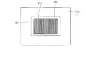
- the piezoelectric device 110 shown in the cross-sectional view of FIG. 8 has an IDT formation region in which the IDT electrode 112 is formed on one main surface 111a of the piezoelectric substrate 111 on which conductive patterns such as the IDT electrode 112 and the pad electrode 113 are formed.
- a frame-like support layer 120 is formed of resin so as to surround the resin, and a resin cover layer 130 is formed on the support layer 120.
- the piezoelectric device 110 is further covered entirely with the outer resin 140, and the IDT space 114 around the IDT electrode 112 is sealed (see, for example, Patent Document 1). JP 2006-352430 A
- the region on the piezoelectric substrate 111 where the vibration propagates (the region where the IDT electrode 112 is formed and the vicinity thereof).
- the support layer 120 that supports the cover layer is formed away from the IDT electrode 112 so as not to adversely affect the cover layer. Since the linear expansion coefficient of the resin support layer 120 is larger than the linear expansion coefficient of the piezoelectric substrate 111, thermal stress is generated between the piezoelectric substrate 111 and the support layer 120 when there is a temperature change. As a result, distortion occurs in the region on which vibration is propagated on 111 and the vibration propagation state changes. As a result, the temperature characteristics of the piezoelectric element formed using the IDT electrode 112 deteriorate.
- the configuration in which the support layer 120 is close to the IDT electrode 112 formed on the piezoelectric substrate 111 is the cross-section in the main part in FIG.
- the cover layer 130 on the support layer 120x bends, and the IDT electrode 112 is deformed.
- the cover layer 130 adheres to the surface, and the characteristics are deteriorated. In particular, when molding with resin, the cover layer 130 is easily bent by the pressure at the time of molding, and the characteristic deterioration is remarkable.
- the design freedom is reduced by increasing the distance between the IDT electrode and the support layer. Furthermore, it goes against the demand for miniaturization of piezoelectric devices.
- the present invention is intended to provide a piezoelectric device that can improve temperature characteristics without changing the distance between the IDT electrode and the support layer.
- the present invention provides a piezoelectric device configured as follows.
- the piezoelectric device includes (a) a piezoelectric substrate, (b) a conductive pattern formed on one main surface of the piezoelectric substrate and including an IDT electrode, and (c) the IDT electrode on the one main surface of the piezoelectric substrate.
- the support layer is formed with a removal portion in which a portion adhered to the one main surface of the piezoelectric substrate is partially removed at least at a plurality of locations near the IDT formation region.
- the removal portion is formed in the support layer in a region close to the IDT formation region, the adhesion area between the support layer and the piezoelectric substrate is small in the region close to the IDT formation region.
- the thermal stress is relaxed and the influence of the thermal stress on the region (IDT formation region and its vicinity) where the vibration on the piezoelectric substrate propagates is reduced, so that the temperature characteristics of the piezoelectric device can be improved.
- the removal part formed in the support layer can have various configurations.
- the removal portion includes a plurality of slits formed so that the support layer extends from an opening formed on an inner peripheral surface facing the IDT region in a direction away from the IDT formation region. It is.
- the bonding area with the piezoelectric substrate is surely reduced by the slit, so that the effect of improving the temperature characteristics is high.
- the removal portion is a hole whose entire circumference is surrounded by the support layer.
- a plurality of holes in one row or two or more rows may be arranged along the outer periphery of the IDT formation region. Or you may arrange
- the support layer penetrates between both main surfaces in contact with the piezoelectric substrate and the cover layer.
- the removal portion that penetrates the support layer can be formed simultaneously with the patterning of the support layer without adding a special process.
- the support layer is formed using a photosensitive resin.
- the support layer can be formed with high accuracy by photolithography.
- the support layer is formed using a photosensitive polyimide resin.
- the support layer is formed using a photosensitive silicone resin.
- the support layer is formed using a photosensitive epoxy resin.
- the cover layer is formed using an epoxy film resin.
- the cover layer is formed using a polyimide film resin.
- a via hole formed by laser processing the support layer and the cover layer at once is further provided.
- the via hole can be formed accurately and inexpensively.
- a via hole formed by sandblasting the support layer and the cover layer in a lump is further provided.
- via holes can be formed at low cost.
- a via hole penetrating the support layer and the cover layer, and an under bump metal formed by Au / Ni electrolytic plating in the via hole are further provided.
- the under bump metal can be formed stably.
- the support layer formed using at least one of a photosensitive resin, a photosensitive polyimide resin, a photosensitive silicone resin, and a photosensitive epoxy resin, and (ii) an epoxy film resin, From the group consisting of the cover layer formed using at least one of polyimide film resin, and (iii) via holes formed by laser processing or sandblasting the support layer and the cover layer at once. Provide two or more selected.
- the temperature characteristics of the piezoelectric device can be improved without changing the distance between the IDT electrode and the support layer.
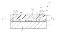
- FIG. 1 is a cross-sectional view of a piezoelectric device 10.
- the piezoelectric device 10 is a SAW (Surface Acoustic Wave) filter in which an element portion is formed on a piezoelectric substrate 11.
- an IDT (Inter (Digital Transducer) electrode 12 which is a comb-like electrode, a pad electrode 13, and a wiring which connects between the IDT electrode 12 and the pad electrode 13. (Not shown) is formed.
- a support layer 20 is formed in a frame shape around the IDT formation region where the IDT electrode 12 is formed. The thickness of the support layer 20 is larger than the thickness of the conductive pattern such as the IDT electrode 12.
- the support layer 20 is also formed on the pad electrode 13.
- a cover layer 30 is disposed on the support layer 20, and the periphery of the IDT electrode 12 formed on the piezoelectric substrate 11 is covered with the support layer 20 and the cover layer 30 that are insulating members to form an IDT space 14. Is done. A surface acoustic wave freely propagates in a portion of the upper surface 11 a of the piezoelectric substrate 11 adjacent to the IDT space 14.
- via holes (through holes) 16 reaching the pad electrodes 13 formed on the upper surface 11 a of the piezoelectric substrate 11 are formed in the support layer 20 and the cover layer 30.
- the via hole 16 is filled with an under bump metal 17, and a solder bump 18 exposed to the outside is formed on the under bump metal 17.
- Piezoelectric device 10 is used, for example, as a module component. After a plurality of piezoelectric devices 10 are mounted on a substrate, the periphery is molded with resin.
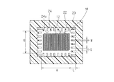
- FIG. 2 is a cross-sectional view schematically showing a cross-sectional view taken along line XX in FIG. In FIG. 2, illustration of the via hole 16 and the under bump metal 17 is omitted.
- the support layer 20 is formed with a plurality of slits 24 as removal portions in a portion close to the IDT formation region where the IDT electrode 12 is formed.
- Each slit 24 is formed in a comb-like shape, that is, parallel to each other with an interval, and extends from an opening 24 a formed in the inner peripheral surface 22 of the support layer 20 in a direction away from the IDT formation region.
- the slit 24 may be formed at least in a portion close to the IDT formation region, and the slit may be extended to a portion far from the IDT formation region.
- the adhesion area between the support layer 20 and the piezoelectric substrate 11 is reduced. Thereby, the thermal stress is relaxed, and the influence of the thermal stress on the region (IDT formation region and its vicinity) where the vibration on the piezoelectric substrate 11 propagates is reduced, so that the temperature characteristics can be improved.
- a conductive pattern including the IDT electrode 12 and the pad electrode 13 is formed on the piezoelectric substrate 11.
- the conductive pattern is formed by a method having height accuracy and surface flatness, such as a deposited metal film, and has a thickness of about 1 to 2 ⁇ m.
- An element part having an element wiring connected to the IDT electrode 12 and the IDT electrode 12 is formed by the conductive pattern.
- a SiO 2 film or a two-layer structure film of SiN / SiO 2 is formed on the surface of the element portion by sputtering.
- pad electrodes 13 serving as a base electrode of the under-bump metal 17 parts that need to be removed SiO 2 film or SiN film is removed SiO 2 film or SiN film by dry etching.
- the support layer 20 is formed so as not to be applied to the vibration part. That is, a photosensitive polyimide resin is applied on the piezoelectric substrate 11, and the IDT space 14 (directly above the IDT electrode 12 and a range of 5 to 15 ⁇ m around the IDT electrode 12) and the slit 24 are opened (removed) by photolithography. At the same time, a range having a width of 100 ⁇ m centering on the dicing line is also opened (removed). In FIG. 2, the size of the IDT space 14 indicated by symbols A and B is in the range of 50 ⁇ m ⁇ 50 ⁇ m to 1000 ⁇ m ⁇ 400 ⁇ m.
- the photosensitive polyimide resin is used for the support layer 20, a photosensitive epoxy resin or a photosensitive silicone resin may be used.
- the thickness of the support layer 20 is 15 ⁇ m, but may be in the range of 10 to 30 ⁇ m.
- the cover layer 30 and the support layer 20 are removed by laser processing at a portion to which the solder ball serving as the external terminal is connected, and the diameter 50 ⁇ A 150 ⁇ m via hole 16 is formed.
- a non-photosensitive epoxy film resin is used for the cover layer 30, but a non-photosensitive polyimide film may be used.
- the cover layer 30 has a thickness of 30 ⁇ m, but may be in the range of 30 to 50 ⁇ m.
- the via hole 16 may be formed by sandblasting.
- the portion of the support layer 20 in the via hole 16 may be formed by a photolithography process when the support layer 20 is formed.
- the under bump metal 17 is formed by forming a thickness of about 1000 nm) by electrolytic plating.
- the under bump metal 17 may be formed by electroless plating.
- the surface of the under bump metal 17 is formed so as to recede (depress) within the range of 0 to 10 ⁇ m from the surface of the cover layer 30.
- solder paste such as Sn—Ag—Cu is printed directly on the under bump metal 17 through a metal mask, and the solder is heated at a temperature at which the solder paste dissolves, for example, about 260 ° C. 17, the flux is removed by a flux cleaning agent, and spherical solder bumps 18 are formed.
- the chip (piece) is cut out by a method such as dicing, and the piezoelectric device 10 is completed.
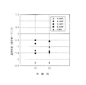
- * (4.0 dBfL) is data about a point on the low frequency side where the filter characteristic is reduced by 4.0 dB from the through level.
- ⁇ (4.0 dBfH) is data about a point on the high frequency side where the filter characteristic is reduced by 4.0 dB from the through level.
- ⁇ (5.0 dBfL) is data about a point on the low frequency side where the filter characteristic is lowered by 5.0 dB from the through level.
- 5.0 dBfH is data about a point on the high frequency side where the filter characteristic is lowered by 5.0 dB from the through level.
- 47 dBfL is data on a point on the low frequency side where the filter characteristic is 47 dB lower than the through level.
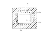
- FIG. 4 is a cross-sectional view schematically showing a cross section obtained by cutting the support layer 20a along the piezoelectric substrate 11 in the same manner as FIG.
- a plurality of holes 26 are formed as removal portions in a portion close to the IDT formation region 12a.
- the hole 26 is formed away from the inner peripheral surface 22a of the support layer 20a, and the entire periphery is surrounded by the support layer 20a.
- the holes 26 arranged in one row along the inner peripheral surface 22 b of the support layer 20 b are illustrated, but the holes can be arranged in various modes, for example, arranged in two or more rows, You may arrange
- the adhesion area between the support layer 20a and the piezoelectric substrate 11 is reduced.
- the thermal stress is relaxed and the influence of the thermal stress on the region (IDT formation region 12a and its vicinity) where the vibration on the piezoelectric substrate 11 propagates is reduced, so that the temperature characteristics can be improved.
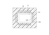
- FIG. 5 is a cross-sectional view schematically showing a cross section of the support layer 20b cut along the piezoelectric substrate 11 in the same manner as FIG.
- a plurality of long holes 28 are formed as removal portions in a portion close to the IDT formation region 12b.
- the long hole 28 is formed away from the inner peripheral surface 22b of the support layer 20b, and the entire circumference is surrounded by the support layer 20b.
- the longitudinal direction of the long hole 28 extends in parallel along the inner peripheral surface 22b of the support layer 20b.
- the long holes 28 arranged in two rows are illustrated, but the long holes can be arranged in various modes, and for example, one row or three or more rows may be arranged.
- the long hole should just be arrange
- the adhesion area between the support layer 20b and the piezoelectric substrate 11 is reduced. Thereby, the thermal stress is relaxed, and the influence of the thermal stress on the region (IDT formation region 12b and its vicinity) where the vibration on the piezoelectric substrate 11 propagates is reduced, so that the temperature characteristics can be improved.
- slits, holes, and long holes as removal portions in the support layer, the temperature characteristics can be improved without changing the distance between the IDT electrode and the support layer. it can.
- the slits, holes, and long holes can be formed simultaneously with the patterning of the support layer without adding a special process.
- the present invention may be applied to a piezoelectric device that is sealed with an outer resin as in the conventional example of FIG. 8, and a removal portion may be provided in the support layer that supports the cover layer.
- the piezoelectric substrate is not limited to the SAW element, and an element portion such as a boundary wave element may be formed.
Landscapes
- Physics & Mathematics (AREA)
- Acoustics & Sound (AREA)
- Surface Acoustic Wave Elements And Circuit Networks Thereof (AREA)
- Piezo-Electric Or Mechanical Vibrators, Or Delay Or Filter Circuits (AREA)
Abstract
Description
11 圧電基板
12 IDT電極
13 パッド電極
16 ビアホール
17 アンダーバンプメタル
20,20a,20b 支持層
24 スリット(除去部)
26 孔(除去部)
28 長孔(除去部)
30 カバー層
・IDT空間サイズ(A×B):作製例(1)及び(2)とも50μm×50μm
・スリット長さ(L):作製例(1)及び(2)とも15μm
・スリット間隔(W):作製例(1)は20μm、作製例(2)は50μm
・スリット幅(S):作製例(1)及び(2)とも50μm
・IDT形成領域と支持層との間隔(D):作製例(1)及び(2)とも30μm
Claims (14)
- 圧電基板と、
前記圧電基板の一方主面に形成され、IDT電極を含む導電パターンと、
前記圧電基板の前記一方主面に、前記IDT電極が形成されたIDT形成領域の周囲を囲むように、かつ前記IDT電極の厚みよりも大きい厚みを有する支持層と、
前記支持層の上に配置され、前記IDT形成領域を覆うカバー層と、
を備えた圧電デバイスにおいて、
前記支持層には、少なくとも前記IDT形成領域に近い領域の複数個所に、前記圧電基板の前記一方主面に接着される部分が部分的に除去された除去部が形成されていることを特徴とする、圧電デバイス。 - 前記除去部は、前記支持層が前記IDT領域に対向する内周面に形成された開口から、前記IDT形成領域から離れる方向に延在するように形成された複数のスリットであることを特徴とする、請求項1に記載の圧電デバイス。
- 前記除去部は、全周が前記支持層で囲まれた孔であることを特徴とする、請求項1に記載の圧電デバイス。
- 前記除去部は、支持層が前記圧電基板と前記カバー層とに接する両主面の間を貫通することを特徴とする、請求項1、2又は3に記載の圧電デバイス。
- 前記支持層は、感光性樹脂を用いて形成されることを特徴とする、請求項1に記載の圧電デバイス。
- 前記支持層は、感光性ポリイミド系樹脂を用いて形成されることを特徴とする、請求項1に記載の圧電デバイス。
- 前記支持層は、感光性シリコーン樹脂を用いて形成されることを特徴とする、請求項1に記載の圧電デバイス。
- 前記支持層は、感光性エポキシ系樹脂を用いて形成されることを特徴とする、請求項1に記載の圧電デバイス。
- 前記カバー層は、エポキシ系フィルム樹脂を用いて形成されることを特徴とする、請求項1に記載の圧電デバイス。
- 前記カバー層は、ポリイミド系フィルム樹脂を用いて形成されることを特徴とする、請求項1に記載の圧電デバイス。
- 前記支持層と前記カバー層とを一括でレーザー加工することにより形成されたビアホールをさらに備えることを特徴とする、請求項1に記載の圧電デバイス。
- 前記支持層と前記カバー層とを一括でサンドブラスト加工することにより形成されたビアホールをさらに備えることを特徴とする、請求項1に記載の圧電デバイス。
- 前記支持層及び前記カバー層を貫通するビアホールと、
前記ビアホール内にAu/Ni電解めっきで形成されたアンダーバンプメタルと、
をさらに備えたことを特徴とする、請求項1に記載の圧電デバイス。 - 感光性樹脂、感光性ポリイミド系樹脂、感光性シリコーン系樹脂、感光性エポキシ系樹脂の少なくとも一つを用いて形成された前記支持層と、
エポキシ系フィルム樹脂、ポリイミド系フィルム樹脂の少なくとも一つを用いて形成された前記カバー層と、
前記支持層と前記カバー層とを一括でレーザー加工又はサンドブラスト加工することにより形成されたビアホールと、
からなる群から選択された2つ以上を備えることを特徴とする、請求項1に記載の圧電デバイス。
Priority Applications (3)
| Application Number | Priority Date | Filing Date | Title |
|---|---|---|---|
| JP2009549998A JP5077357B2 (ja) | 2008-01-17 | 2009-01-06 | 圧電デバイス |
| CN200980101968.0A CN101911485B (zh) | 2008-01-17 | 2009-01-06 | 压电器件 |
| US12/836,595 US8067879B2 (en) | 2008-01-17 | 2010-07-15 | Piezoelectric device |
Applications Claiming Priority (2)
| Application Number | Priority Date | Filing Date | Title |
|---|---|---|---|
| JP2008-008476 | 2008-01-17 | ||
| JP2008008476 | 2008-01-17 |
Related Child Applications (1)
| Application Number | Title | Priority Date | Filing Date |
|---|---|---|---|
| US12/836,595 Continuation US8067879B2 (en) | 2008-01-17 | 2010-07-15 | Piezoelectric device |
Publications (1)
| Publication Number | Publication Date |
|---|---|
| WO2009090895A1 true WO2009090895A1 (ja) | 2009-07-23 |
Family
ID=40885286
Family Applications (1)
| Application Number | Title | Priority Date | Filing Date |
|---|---|---|---|
| PCT/JP2009/050027 Ceased WO2009090895A1 (ja) | 2008-01-17 | 2009-01-06 | 圧電デバイス |
Country Status (4)
| Country | Link |
|---|---|
| US (1) | US8067879B2 (ja) |
| JP (1) | JP5077357B2 (ja) |
| CN (1) | CN101911485B (ja) |
| WO (1) | WO2009090895A1 (ja) |
Cited By (8)
| Publication number | Priority date | Publication date | Assignee | Title |
|---|---|---|---|---|
| JP2009231389A (ja) * | 2008-03-19 | 2009-10-08 | Fujikura Ltd | 半導体パッケージ及びその製造方法 |
| JP2011130150A (ja) * | 2009-12-17 | 2011-06-30 | Kyocera Corp | 弾性波装置及びその製造方法 |
| WO2012050016A1 (ja) * | 2010-10-15 | 2012-04-19 | 株式会社村田製作所 | 弾性表面波装置 |
| JP2012182481A (ja) * | 2012-05-07 | 2012-09-20 | Fujikura Ltd | 半導体パッケージ及びその製造方法 |
| US8530979B2 (en) | 2008-04-04 | 2013-09-10 | Fujikura Ltd. | Semiconductor package and method for manufacturing the same |
| JP2014014131A (ja) * | 2013-08-30 | 2014-01-23 | Taiyo Yuden Co Ltd | 弾性波デバイス内蔵モジュール及び通信装置 |
| US9478213B2 (en) | 2012-06-28 | 2016-10-25 | Taiyo Yuden Co., Ltd. | Acoustic wave device built-in module and communication device |
| US20210098683A1 (en) | 2019-09-26 | 2021-04-01 | Taiyo Yuden Co., Ltd. | Electronic device |
Families Citing this family (6)
| Publication number | Priority date | Publication date | Assignee | Title |
|---|---|---|---|---|
| EP2913858B1 (en) * | 2012-10-29 | 2018-06-13 | Kyocera Corporation | Multilayered piezo element, as well as piezo actuator, injection apparatus, and fuel injection system provided with said element |
| JP6179593B2 (ja) * | 2013-05-27 | 2017-08-16 | 株式会社村田製作所 | 弾性表面波装置 |
| JP6070910B1 (ja) | 2015-03-16 | 2017-02-01 | 株式会社村田製作所 | 弾性波装置及びその製造方法 |
| CN109075768B (zh) * | 2016-04-14 | 2022-06-24 | 株式会社村田制作所 | 弹性波装置及其制造方法 |
| WO2019044178A1 (ja) * | 2017-08-31 | 2019-03-07 | 株式会社村田製作所 | 弾性波装置およびそれを備えた弾性波モジュール |
| US11581870B2 (en) * | 2019-09-27 | 2023-02-14 | Skyworks Solutions, Inc. | Stacked acoustic wave resonator package with laser-drilled VIAS |
Citations (5)
| Publication number | Priority date | Publication date | Assignee | Title |
|---|---|---|---|---|
| JPH1012757A (ja) * | 1996-06-25 | 1998-01-16 | Kokusai Electric Co Ltd | マイクロパッケージ |
| JPH11251866A (ja) * | 1998-02-27 | 1999-09-17 | Tdk Corp | チップ素子及びチップ素子の製造方法 |
| JP2006352430A (ja) * | 2005-06-15 | 2006-12-28 | Murata Mfg Co Ltd | 圧電デバイスとその製造方法 |
| JP2007019943A (ja) * | 2005-07-08 | 2007-01-25 | Alps Electric Co Ltd | 表面弾性波ディバイス |
| JP2007318058A (ja) * | 2006-04-27 | 2007-12-06 | Murata Mfg Co Ltd | 電子部品及びその製造方法 |
Family Cites Families (5)
| Publication number | Priority date | Publication date | Assignee | Title |
|---|---|---|---|---|
| JPS6412757A (en) * | 1987-07-07 | 1989-01-17 | Canon Kk | Recording paper ejecting device for communication equipment |
| US7011134B2 (en) * | 2000-10-13 | 2006-03-14 | Chien-Min Sung | Casting method for producing surface acoustic wave devices |
| JP2005348273A (ja) | 2004-06-04 | 2005-12-15 | Murata Mfg Co Ltd | 弾性表面波装置 |
| JP4518255B2 (ja) | 2004-12-22 | 2010-08-04 | セイコーエプソン株式会社 | 弾性表面波素子および電子機器 |
| JP2007073595A (ja) | 2005-09-05 | 2007-03-22 | Renesas Technology Corp | 半導体装置の製造方法 |
-
2009
- 2009-01-06 JP JP2009549998A patent/JP5077357B2/ja not_active Expired - Fee Related
- 2009-01-06 CN CN200980101968.0A patent/CN101911485B/zh not_active Expired - Fee Related
- 2009-01-06 WO PCT/JP2009/050027 patent/WO2009090895A1/ja not_active Ceased
-
2010
- 2010-07-15 US US12/836,595 patent/US8067879B2/en not_active Expired - Fee Related
Patent Citations (5)
| Publication number | Priority date | Publication date | Assignee | Title |
|---|---|---|---|---|
| JPH1012757A (ja) * | 1996-06-25 | 1998-01-16 | Kokusai Electric Co Ltd | マイクロパッケージ |
| JPH11251866A (ja) * | 1998-02-27 | 1999-09-17 | Tdk Corp | チップ素子及びチップ素子の製造方法 |
| JP2006352430A (ja) * | 2005-06-15 | 2006-12-28 | Murata Mfg Co Ltd | 圧電デバイスとその製造方法 |
| JP2007019943A (ja) * | 2005-07-08 | 2007-01-25 | Alps Electric Co Ltd | 表面弾性波ディバイス |
| JP2007318058A (ja) * | 2006-04-27 | 2007-12-06 | Murata Mfg Co Ltd | 電子部品及びその製造方法 |
Cited By (10)
| Publication number | Priority date | Publication date | Assignee | Title |
|---|---|---|---|---|
| JP2009231389A (ja) * | 2008-03-19 | 2009-10-08 | Fujikura Ltd | 半導体パッケージ及びその製造方法 |
| US8530979B2 (en) | 2008-04-04 | 2013-09-10 | Fujikura Ltd. | Semiconductor package and method for manufacturing the same |
| JP5417320B2 (ja) * | 2008-04-04 | 2014-02-12 | 株式会社フジクラ | 半導体パッケージ |
| JP2011130150A (ja) * | 2009-12-17 | 2011-06-30 | Kyocera Corp | 弾性波装置及びその製造方法 |
| WO2012050016A1 (ja) * | 2010-10-15 | 2012-04-19 | 株式会社村田製作所 | 弾性表面波装置 |
| JP2012182481A (ja) * | 2012-05-07 | 2012-09-20 | Fujikura Ltd | 半導体パッケージ及びその製造方法 |
| US9478213B2 (en) | 2012-06-28 | 2016-10-25 | Taiyo Yuden Co., Ltd. | Acoustic wave device built-in module and communication device |
| JP2014014131A (ja) * | 2013-08-30 | 2014-01-23 | Taiyo Yuden Co Ltd | 弾性波デバイス内蔵モジュール及び通信装置 |
| US20210098683A1 (en) | 2019-09-26 | 2021-04-01 | Taiyo Yuden Co., Ltd. | Electronic device |
| US11751480B2 (en) | 2019-09-26 | 2023-09-05 | Taiyo Yuden Co., Ltd. | Electronic device |
Also Published As
| Publication number | Publication date |
|---|---|
| CN101911485B (zh) | 2014-07-09 |
| US20100277035A1 (en) | 2010-11-04 |
| CN101911485A (zh) | 2010-12-08 |
| JPWO2009090895A1 (ja) | 2011-05-26 |
| US8067879B2 (en) | 2011-11-29 |
| JP5077357B2 (ja) | 2012-11-21 |
Similar Documents
| Publication | Publication Date | Title |
|---|---|---|
| JP5077357B2 (ja) | 圧電デバイス | |
| JP6603377B2 (ja) | 弾性波装置および電子部品 | |
| JP6409785B2 (ja) | 弾性波装置及びその製造方法 | |
| JP6288111B2 (ja) | 弾性波フィルタデバイス | |
| JP5797356B2 (ja) | 弾性波装置および弾性波モジュール | |
| JP5277971B2 (ja) | 弾性表面波デバイス | |
| JP5591163B2 (ja) | 弾性波装置およびその製造方法 | |
| JP2007318058A (ja) | 電子部品及びその製造方法 | |
| JP2019103127A (ja) | 弾性波装置 | |
| JP5848079B2 (ja) | 弾性波デバイス及びその製造方法 | |
| CN105870317B (zh) | 压电元件装置 | |
| JP5269301B2 (ja) | 弾性表面波装置 | |
| US20210013867A1 (en) | Acoustic wave device | |
| JP4655796B2 (ja) | 弾性境界波装置の製造方法及び弾性境界波装置 | |
| JP2011182153A (ja) | 弾性波デバイス | |
| JP5467375B2 (ja) | 弾性表面波デバイス | |
| JP2009182741A (ja) | 弾性境界波デバイス及びその製造方法 | |
| JP6352844B2 (ja) | 多数個取り回路配線基板および弾性表面波装置 | |
| JP5431198B2 (ja) | 弾性波デバイス | |
| JP2010010512A (ja) | 電子デバイス及びその製造方法 |
Legal Events
| Date | Code | Title | Description |
|---|---|---|---|
| WWE | Wipo information: entry into national phase |
Ref document number: 200980101968.0 Country of ref document: CN |
|
| 121 | Ep: the epo has been informed by wipo that ep was designated in this application |
Ref document number: 09702448 Country of ref document: EP Kind code of ref document: A1 |
|
| WWE | Wipo information: entry into national phase |
Ref document number: 2009549998 Country of ref document: JP |
|
| NENP | Non-entry into the national phase |
Ref country code: DE |
|
| 122 | Ep: pct application non-entry in european phase |
Ref document number: 09702448 Country of ref document: EP Kind code of ref document: A1 |