US9966473B2 - Manufacturing method of semiconductor device - Google Patents
Manufacturing method of semiconductor device Download PDFInfo
- Publication number
- US9966473B2 US9966473B2 US15/147,279 US201615147279A US9966473B2 US 9966473 B2 US9966473 B2 US 9966473B2 US 201615147279 A US201615147279 A US 201615147279A US 9966473 B2 US9966473 B2 US 9966473B2
- Authority
- US
- United States
- Prior art keywords
- transistor
- conductor
- insulator
- semiconductor
- oxide semiconductor
- Prior art date
- Legal status (The legal status is an assumption and is not a legal conclusion. Google has not performed a legal analysis and makes no representation as to the accuracy of the status listed.)
- Expired - Fee Related, expires
Links
Images


Classifications
-
- H—ELECTRICITY
- H10—SEMICONDUCTOR DEVICES; ELECTRIC SOLID-STATE DEVICES NOT OTHERWISE PROVIDED FOR
- H10D—INORGANIC ELECTRIC SEMICONDUCTOR DEVICES
- H10D30/00—Field-effect transistors [FET]
- H10D30/60—Insulated-gate field-effect transistors [IGFET]
- H10D30/67—Thin-film transistors [TFT]
- H10D30/674—Thin-film transistors [TFT] characterised by the active materials
- H10D30/6755—Oxide semiconductors, e.g. zinc oxide, copper aluminium oxide or cadmium stannate
-
- H01L29/7869—
-
- H01L29/24—
-
- H01L29/66969—
-
- H01L29/78618—
-
- H01L29/78696—
-
- H—ELECTRICITY
- H10—SEMICONDUCTOR DEVICES; ELECTRIC SOLID-STATE DEVICES NOT OTHERWISE PROVIDED FOR
- H10D—INORGANIC ELECTRIC SEMICONDUCTOR DEVICES
- H10D30/00—Field-effect transistors [FET]
- H10D30/60—Insulated-gate field-effect transistors [IGFET]
- H10D30/62—Fin field-effect transistors [FinFET]
-
- H—ELECTRICITY
- H10—SEMICONDUCTOR DEVICES; ELECTRIC SOLID-STATE DEVICES NOT OTHERWISE PROVIDED FOR
- H10D—INORGANIC ELECTRIC SEMICONDUCTOR DEVICES
- H10D30/00—Field-effect transistors [FET]
- H10D30/60—Insulated-gate field-effect transistors [IGFET]
- H10D30/67—Thin-film transistors [TFT]
- H10D30/6704—Thin-film transistors [TFT] having supplementary regions or layers in the thin films or in the insulated bulk substrates for controlling properties of the device
- H10D30/6713—Thin-film transistors [TFT] having supplementary regions or layers in the thin films or in the insulated bulk substrates for controlling properties of the device characterised by the properties of the source or drain regions, e.g. compositions or sectional shapes
-
- H—ELECTRICITY
- H10—SEMICONDUCTOR DEVICES; ELECTRIC SOLID-STATE DEVICES NOT OTHERWISE PROVIDED FOR
- H10D—INORGANIC ELECTRIC SEMICONDUCTOR DEVICES
- H10D30/00—Field-effect transistors [FET]
- H10D30/60—Insulated-gate field-effect transistors [IGFET]
- H10D30/67—Thin-film transistors [TFT]
- H10D30/6729—Thin-film transistors [TFT] characterised by the electrodes
- H10D30/673—Thin-film transistors [TFT] characterised by the electrodes characterised by the shapes, relative sizes or dispositions of the gate electrodes
- H10D30/6733—Multi-gate TFTs
- H10D30/6734—Multi-gate TFTs having gate electrodes arranged on both top and bottom sides of the channel, e.g. dual-gate TFTs
-
- H—ELECTRICITY
- H10—SEMICONDUCTOR DEVICES; ELECTRIC SOLID-STATE DEVICES NOT OTHERWISE PROVIDED FOR
- H10D—INORGANIC ELECTRIC SEMICONDUCTOR DEVICES
- H10D30/00—Field-effect transistors [FET]
- H10D30/60—Insulated-gate field-effect transistors [IGFET]
- H10D30/67—Thin-film transistors [TFT]
- H10D30/6757—Thin-film transistors [TFT] characterised by the structure of the channel, e.g. transverse or longitudinal shape or doping profile
-
- H—ELECTRICITY
- H10—SEMICONDUCTOR DEVICES; ELECTRIC SOLID-STATE DEVICES NOT OTHERWISE PROVIDED FOR
- H10D—INORGANIC ELECTRIC SEMICONDUCTOR DEVICES
- H10D62/00—Semiconductor bodies, or regions thereof, of devices having potential barriers
- H10D62/80—Semiconductor bodies, or regions thereof, of devices having potential barriers characterised by the materials
-
- H—ELECTRICITY
- H10—SEMICONDUCTOR DEVICES; ELECTRIC SOLID-STATE DEVICES NOT OTHERWISE PROVIDED FOR
- H10D—INORGANIC ELECTRIC SEMICONDUCTOR DEVICES
- H10D84/00—Integrated devices formed in or on semiconductor substrates that comprise only semiconducting layers, e.g. on Si wafers or on GaAs-on-Si wafers
- H10D84/01—Manufacture or treatment
- H10D84/02—Manufacture or treatment characterised by using material-based technologies
- H10D84/08—Manufacture or treatment characterised by using material-based technologies using combinations of technologies, e.g. using both Si and SiC technologies or using both Si and Group III-V technologies
-
- H—ELECTRICITY
- H10—SEMICONDUCTOR DEVICES; ELECTRIC SOLID-STATE DEVICES NOT OTHERWISE PROVIDED FOR
- H10D—INORGANIC ELECTRIC SEMICONDUCTOR DEVICES
- H10D86/00—Integrated devices formed in or on insulating or conducting substrates, e.g. formed in silicon-on-insulator [SOI] substrates or on stainless steel or glass substrates
- H10D86/01—Manufacture or treatment
- H10D86/021—Manufacture or treatment of multiple TFTs
-
- H—ELECTRICITY
- H10—SEMICONDUCTOR DEVICES; ELECTRIC SOLID-STATE DEVICES NOT OTHERWISE PROVIDED FOR
- H10D—INORGANIC ELECTRIC SEMICONDUCTOR DEVICES
- H10D86/00—Integrated devices formed in or on insulating or conducting substrates, e.g. formed in silicon-on-insulator [SOI] substrates or on stainless steel or glass substrates
- H10D86/40—Integrated devices formed in or on insulating or conducting substrates, e.g. formed in silicon-on-insulator [SOI] substrates or on stainless steel or glass substrates characterised by multiple TFTs
- H10D86/421—Integrated devices formed in or on insulating or conducting substrates, e.g. formed in silicon-on-insulator [SOI] substrates or on stainless steel or glass substrates characterised by multiple TFTs having a particular composition, shape or crystalline structure of the active layer
- H10D86/423—Integrated devices formed in or on insulating or conducting substrates, e.g. formed in silicon-on-insulator [SOI] substrates or on stainless steel or glass substrates characterised by multiple TFTs having a particular composition, shape or crystalline structure of the active layer comprising semiconductor materials not belonging to the Group IV, e.g. InGaZnO
-
- H—ELECTRICITY
- H10—SEMICONDUCTOR DEVICES; ELECTRIC SOLID-STATE DEVICES NOT OTHERWISE PROVIDED FOR
- H10D—INORGANIC ELECTRIC SEMICONDUCTOR DEVICES
- H10D86/00—Integrated devices formed in or on insulating or conducting substrates, e.g. formed in silicon-on-insulator [SOI] substrates or on stainless steel or glass substrates
- H10D86/40—Integrated devices formed in or on insulating or conducting substrates, e.g. formed in silicon-on-insulator [SOI] substrates or on stainless steel or glass substrates characterised by multiple TFTs
- H10D86/60—Integrated devices formed in or on insulating or conducting substrates, e.g. formed in silicon-on-insulator [SOI] substrates or on stainless steel or glass substrates characterised by multiple TFTs wherein the TFTs are in active matrices
-
- H—ELECTRICITY
- H10—SEMICONDUCTOR DEVICES; ELECTRIC SOLID-STATE DEVICES NOT OTHERWISE PROVIDED FOR
- H10D—INORGANIC ELECTRIC SEMICONDUCTOR DEVICES
- H10D87/00—Integrated devices comprising both bulk components and either SOI or SOS components on the same substrate
-
- H—ELECTRICITY
- H10—SEMICONDUCTOR DEVICES; ELECTRIC SOLID-STATE DEVICES NOT OTHERWISE PROVIDED FOR
- H10D—INORGANIC ELECTRIC SEMICONDUCTOR DEVICES
- H10D88/00—Three-dimensional [3D] integrated devices
-
- H—ELECTRICITY
- H10—SEMICONDUCTOR DEVICES; ELECTRIC SOLID-STATE DEVICES NOT OTHERWISE PROVIDED FOR
- H10D—INORGANIC ELECTRIC SEMICONDUCTOR DEVICES
- H10D99/00—Subject matter not provided for in other groups of this subclass
Definitions
- the present invention relates to, for example, a transistor, a semiconductor device, and manufacturing methods thereof.
- the present invention relates to, for example, a display device, a light-emitting device, a lighting device, a power storage device, a memory device, a processor, an imaging device, and an electronic device.
- the present invention relates to methods for manufacturing an oxide, a display device, a liquid crystal display device, a light-emitting device, a memory device, a processor, an imaging device, and an electronic device.
- the present invention relates to methods for driving a semiconductor device, a display device, a liquid crystal display device, a light-emitting device, a memory device, a processor, an imaging device, and an electronic device.
- one embodiment of the present invention is not limited to the above technical field.
- the technical field of one embodiment of the invention disclosed in this specification and the like relates to an object, a method, or a manufacturing method.
- One embodiment of the present invention relates to a process, a machine, manufacture, or a composition of matter.
- a semiconductor device refers to any device that can function by utilizing semiconductor characteristics.
- a display device, a light-emitting device, a lighting device, an electro-optical device, a semiconductor circuit, and an electronic device include a semiconductor device in some cases.
- a technique for forming a transistor by using a semiconductor over a substrate having an insulating surface has attracted attention.
- the transistor is applied to a wide range of semiconductor devices such as an integrated circuit and a display device.
- Silicon is known as a semiconductor applicable to a transistor.
- amorphous silicon As silicon which is used as a semiconductor of a transistor, either amorphous silicon or polycrystalline silicon is used depending on the purpose.
- amorphous silicon In the case of a transistor included in a large display device, it is preferable to use amorphous silicon, which can be used to form a film on a large substrate with the established technique.
- polycrystalline silicon In the case of a transistor included in a high-performance display device where driver circuits are formed over the same substrate, it is preferable to use polycrystalline silicon, which can be used to form a transistor having high field-effect mobility.
- As a method for forming polycrystalline silicon high-temperature heat treatment or laser light treatment which is performed on amorphous silicon has been known.
- transistors including oxide semiconductors (typically, In—Ga—Zn oxide) have been actively developed.
- Oxide semiconductors have been researched since early times. In 1988, there was a disclosure of a crystal In—Ga—Zn oxide that can be used for a semiconductor element (see Patent Document 1). In 1995, a transistor including an oxide semiconductor was invented, and its electrical characteristics were disclosed (see Patent Document 2).
- a transistor including an amorphous oxide semiconductor is disclosed (see Patent Document 3).
- An oxide semiconductor can be formed by a sputtering method or the like, and thus can be used for a semiconductor of a transistor in a large display device.
- a transistor including an oxide semiconductor has high field-effect mobility; therefore, a high-performance display device where driver circuits are formed over the same substrate can be obtained.
- capital investment can be reduced because part of production equipment for a transistor including amorphous silicon can be retrofitted and utilized.
- Non-Patent Document 1 Recent research and development results show that using a crystalline oxide semiconductor increases the reliability of a transistor as compared to the case of using an amorphous oxide semiconductor.
- a transistor having a high field-effect mobility can be obtained by a well potential formed using an active layer including an oxide semiconductor (see Patent Document 4). It is known that a transistor including an oxide semiconductor has an extremely low leakage current in an off state. For example, a low power consumption CPU and the like utilizing a characteristic of a low leakage current of the transistor including an oxide semiconductor are disclosed (see Patent Document 5).
- Another object of one embodiment of the present invention is to achieve high integration, high performance, high reliability, and high productivity also of a semiconductor device including the transistor. Another object is to provide a novel semiconductor device. Note that the descriptions of these objects do not disturb the existence of other objects. Note that one embodiment of the present invention does not necessarily achieve all the objects listed above. Other objects will be apparent from and can be derived from the description of the specification, the drawings, the claims, and the like.
- One embodiment of the present invention is a manufacturing method of a semiconductor device including the steps of: forming a semiconductor and a first conductor over a substrate; forming a sacrificial layer over the first conductor; forming a first insulator so as to cover the semiconductor, the first conductor, and the sacrificial layer; exposing a top surface of the sacrificial layer by a chemical mechanical polishing method; removing the sacrificial layer to form an opening in the first insulator, so that part of the first conductor is exposed; forming a first electrode and a second electrode by removing part of the first conductor; forming a second insulator so as to cover the first insulator and the opening; forming a second conductor over the second insulator; and removing part of the second conductor.
- the part of the second conductor is removed by a chemical mechanical polishing method.
- One embodiment of the present invention is a manufacturing method of a semiconductor device including the steps of: forming a semiconductor over a substrate; forming a sacrificial layer over the semiconductor; forming a low resistance region by adding an impurity to part of the semiconductor; forming a first insulator so as to cover the semiconductor and the sacrificial layer; exposing a top surface of the sacrificial layer by a chemical mechanical polishing method; removing the sacrificial layer to form an opening in the first insulator, so that part of the semiconductor is exposed; forming a second insulator so as to cover the first insulator and the opening; forming a conductor over the second insulator; and removing part of the conductor.
- part of the conductor is removed by a chemical mechanical polishing method.
- the sacrificial layer is removed by a wet etching method.
- the first insulator preferably contains oxygen.
- One embodiment of the present invention is a manufacturing method of an electronic device that includes any of the above semiconductor devices.
- transistors that have little variation in characteristics even when being miniaturized can be provided.
- a transistor with low parasitic capacitance can be provided.
- a transistor with high operation frequency can be provided. It is also possible to provide a transistor with stable electrical characteristics. Further alternatively, one embodiment of the invention disclosed can provide a transistor whose amount of on-state current is large.
- the channel length of the transistor can be easily adjusted.
- oxygen can be supplied to the oxide semiconductor. Oxygen vacancies in the oxide semiconductor are filled with supplied oxygen, whereby the reliability of a transistor using the oxide semiconductor can be increased.
- FIGS. 1A to 1H are cross-sectional views illustrating one embodiment of a manufacturing method of a semiconductor device.
- FIGS. 2A to 2F are cross-sectional views illustrating one embodiment of a semiconductor device.
- FIGS. 3A to 3F are cross-sectional views illustrating one embodiment of a manufacturing method of a semiconductor device.
- FIGS. 4A to 4D are cross-sectional views illustrating one embodiment of a manufacturing method of a semiconductor device.
- FIGS. 5A to 5C are a top view and cross-sectional views illustrating one embodiment of a semiconductor device.
- FIGS. 6A to 6F are cross-sectional views illustrating one embodiment of a manufacturing method of a semiconductor device.
- FIGS. 7A to 7F are cross-sectional views illustrating one embodiment of a manufacturing method of a semiconductor device.
- FIGS. 8A to 8F are cross-sectional views illustrating one embodiment of a manufacturing method of a semiconductor device.
- FIGS. 9A to 9D are cross-sectional views illustrating one embodiment of a manufacturing method of a semiconductor device.
- FIGS. 10A to 10C are a top view and cross-sectional views illustrating one embodiment of a semiconductor device.
- FIGS. 11A to 11H are cross-sectional views illustrating one embodiment of a manufacturing method of a semiconductor device.
- FIGS. 12A to 12F are cross-sectional views illustrating one embodiment of a manufacturing method of a semiconductor device.
- FIGS. 13A to 13F are cross-sectional views illustrating one embodiment of a manufacturing method of a semiconductor device.
- FIGS. 14A to 14F are cross-sectional views illustrating one embodiment of a manufacturing method of a semiconductor device.
- FIGS. 15A to 15C are a top view and cross-sectional views illustrating one embodiment of a semiconductor device.
- FIGS. 16A to 16H are cross-sectional views each illustrating one embodiment of a semiconductor device.
- FIGS. 17A to 17F are cross-sectional views illustrating one embodiment of a manufacturing method of a semiconductor device.
- FIGS. 18A to 18F are cross-sectional views illustrating one embodiment of a manufacturing method of a semiconductor device.
- FIGS. 19A and 19B are cross-sectional views illustrating one embodiment of a manufacturing method of a semiconductor device.
- FIGS. 20A to 20C are a top view and cross-sectional views illustrating one embodiment of a semiconductor device.
- FIGS. 21A to 21H are cross-sectional views illustrating one embodiment of a manufacturing method of a semiconductor device.
- FIGS. 22A to 22F are cross-sectional views illustrating one embodiment of a manufacturing method of a semiconductor device.
- FIGS. 23A to 23F are cross-sectional views illustrating one embodiment of a manufacturing method of a semiconductor device.
- FIGS. 24A to 24D are cross-sectional views illustrating one embodiment of a manufacturing method of a semiconductor device.
- FIGS. 25A to 25C are a top view and cross-sectional views illustrating one embodiment of a semiconductor device.
- FIGS. 26A and 26B show atomic ratios of an oxide semiconductor of one embodiment of the present invention.
- FIGS. 27A to 27E show structural analysis of a CAAC-OS and a single crystal oxide semiconductor by XRD and selected-area electron diffraction patterns of a CAAC-OS.
- FIGS. 28A to 28E show a cross-sectional TEM image and plan-view TEM images of a CAAC-OS and images obtained through analysis thereof.
- FIGS. 29A to 29D show electron diffraction patterns and a cross-sectional TEM image of an nc-OS.
- FIGS. 30A and 30B show cross-sectional TEM images of an a-like OS.
- FIG. 31 shows a change in crystal part of an In—Ga—Zn oxide induced by electron irradiation.
- FIGS. 32A and 32B are circuit diagrams each illustrating a semiconductor device of one embodiment of the present invention.
- FIG. 33 is a cross-sectional view illustrating a semiconductor device of one embodiment of the present invention.
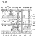
- FIG. 34 is a cross-sectional view illustrating a semiconductor device of one embodiment of the present invention.
- FIG. 35 is a cross-sectional view illustrating a semiconductor device of one embodiment of the present invention.
- FIGS. 36A and 36B are circuit diagrams each illustrating a memory device of one embodiment of the present invention.
- FIG. 37 is a cross-sectional view illustrating a semiconductor device of one embodiment of the present invention.
- FIG. 38 is a cross-sectional view illustrating a semiconductor device of one embodiment of the present invention.
- FIG. 39 is a cross-sectional view illustrating a semiconductor device of one embodiment of the present invention.
- FIG. 40 is a circuit diagram illustrating a semiconductor device of one embodiment of the present invention.
- FIG. 41 is a cross-sectional view illustrating a semiconductor device of one embodiment of the present invention.
- FIGS. 42A to 42E are circuit diagrams illustrating a semiconductor device of one embodiment of the present invention.
- FIGS. 43A and 43B are each a top view of a semiconductor device according to one embodiment of the present invention.
- FIGS. 44A and 44B are block diagrams illustrating a semiconductor device according to one embodiment of the present invention.
- FIGS. 45A and 45B are each a cross-sectional view illustrating a semiconductor device according to one embodiment of the present invention.
- FIGS. 46A and 46B are each a cross-sectional view illustrating a semiconductor device according to one embodiment of the present invention.
- FIGS. 47 A 1 , 47 A 2 , 47 A 3 , 47 B 1 , 47 B 2 , and 47 B 3 are perspective views and cross-sectional views of semiconductor devices according to one embodiment of the present invention.
- FIG. 48 is a block diagram illustrating a semiconductor device of one embodiment of the present invention.
- FIG. 49 is a circuit diagram of a semiconductor device according to one embodiment of the present invention.
- FIGS. 50A to 50C are a circuit diagram, a top view, and a cross-sectional view illustrating a semiconductor device of one embodiment of the present invention.
- FIGS. 51A and 51B are a circuit diagram and a cross-sectional view illustrating a semiconductor device of one embodiment of the present invention.
- FIGS. 52A to 52F are perspective views each illustrating an electronic device of one embodiment of the present invention.
- semiconductor device in this specification and the like means all devices which can operate by utilizing semiconductor characteristics.
- a semiconductor element such as a transistor, a semiconductor circuit, an arithmetic device, and a memory device are each an embodiment of a semiconductor device.
- An imaging device, a display device, a liquid crystal display device, a light-emitting device, an electro-optical device, a power generation device (including a thin film solar cell, an organic thin film solar cell, and the like), and an electronic device may each include a semiconductor device.
- a transistor is an element having at least three terminals: a gate, a drain, and a source.
- the transistor has a channel region between the drain (a drain terminal, a drain region, or a drain electrode) and the source (a source terminal, a source region, or a source electrode), and current can flow through the drain, the channel region, and the source.
- a channel region refers to a region through which current mainly flows.
- Source and drain Functions of a source and a drain are sometimes replaced with each other when a transistor of opposite polarity is used or when the direction of current flowing is changed in circuit operation, for example. Therefore, the terms “source” and “drain” can be replaced with each other in this specification and the like.
- a silicon oxynitride film refers to a film in which the proportion of oxygen is higher than that of nitrogen.
- the silicon oxynitride film preferably contains oxygen, nitrogen, silicon, and hydrogen at concentrations ranging from 55 atomic % to 65 atomic %, 1 atomic % to 20 atomic %, 25 atomic % to 35 atomic %, and 0.1 atomic % to 10 atomic %, respectively.
- a silicon nitride oxide film refers to a film in which the proportion of nitrogen is higher than that of oxygen.
- the silicon nitride oxide film preferably contains nitrogen, oxygen, silicon, and hydrogen at concentrations ranging from 55 atomic % to 65 atomic %, 1 atomic % to 20 atomic %, 25 atomic % to 35 atomic %, and 0.1 atomic % to 10 atomic %, respectively.
- the terms “film” and “layer” can be interchanged with each other.
- the term “conductive layer” can be changed into the term “conductive film” in some cases.
- the term “insulating film” can be changed into the term “insulating layer” in some cases.
- the term “parallel” indicates that the angle formed between two straight lines is greater than or equal to ⁇ 10° and less than or equal to 10°, and accordingly also includes the case where the angle is greater than or equal to ⁇ 5° and less than or equal to 5°.
- the term “substantially parallel” indicates that the angle formed between two straight lines is greater than or equal to ⁇ 30° and less than or equal to 30°.
- the term “perpendicular” indicates that the angle formed between two straight lines is greater than or equal to 80° and less than or equal to 100°, and accordingly also includes the case where the angle is greater than or equal to 85° and less than or equal to 95°.
- the term “substantially perpendicular” indicates that the angle formed between two straight lines is greater than or equal to 60° and less than or equal to 120°.
- an explicit description “X and Y are connected” means that X and Y are electrically connected, X and Y are functionally connected, and X and Y are directly connected. Accordingly, without being limited to a predetermined connection relationship, for example, a connection relationship shown in drawings or texts, another connection relationship is included in the drawings or the texts.
- each of X and Y denotes an object (e.g., a device, an element, a circuit, a wiring, an electrode, a terminal, a conductor, or a layer).
- object e.g., a device, an element, a circuit, a wiring, an electrode, a terminal, a conductor, or a layer.
- Examples of the case where X and Y are directly connected include the case where an element that enables electrical connection between X and Y (e.g., a switch, a transistor, a capacitor, an inductor, a resistor, a diode, a display element, a light-emitting element, or a load) is not connected between X and Y, and the case where X and Y are connected without the element that enables electrical connection between X and Y provided therebetween.
- an element that enables electrical connection between X and Y e.g., a switch, a transistor, a capacitor, an inductor, a resistor, a diode, a display element, a light-emitting element, or a load
- one or more elements that enable electrical connection between X and Y can be connected between X and Y.
- the switch is controlled to be turned on or off. That is, the switch is conducting or not conducting (is turned on or off) to determine whether current flows therethrough or not.
- the switch has a function of selecting and changing a current path. Note that the case where X and Y are electrically connected includes the case where X and Y are directly connected.
- one or more circuits that enable functional connection between X and Y can be connected between X and Y.
- a logic circuit such as an inverter, a NAND circuit, or a NOR circuit
- a signal converter circuit such as a D/A converter circuit, an A/D converter circuit, or a gamma correction circuit
- a potential level converter circuit such as a power supply circuit (e.g., a step-up circuit or a step-down circuit) or a level shifter circuit for changing the potential level of a signal
- a voltage source e.g., a step-up circuit or a step-down circuit
- a level shifter circuit for changing the potential level of a signal
- a voltage source e.g., a step-up circuit or a step-down circuit
- an amplifier circuit such as a circuit that can increase signal amplitude, the amount of current, or the like, an operational amplifier, a differential amplifier circuit, a source follower circuit, or a buffer circuit
- X and Y are functionally connected.
- the case where X and Y are functionally connected includes the case where X and Y are directly connected and X and Y are electrically connected.
- an explicit description “X and Y are electrically connected” means that X and Y are electrically connected (i.e., the case where X and Y are connected with another element or another circuit provided therebetween), X and Y are functionally connected (i.e., the case where X and Y are functionally connected with another circuit provided therebetween), and X and Y are directly connected (i.e., the case where X and Y are connected without another element or another circuit provided therebetween). That is, in this specification and the like, the explicit description “X and Y are electrically connected” is the same as the explicit description “X and Y are connected.”
- the expressions include, for example, “X, Y, a source (or a first terminal or the like) of a transistor, and a drain (or a second terminal or the like) of the transistor are electrically connected to each other, and X, the source (or the first terminal or the like) of the transistor, the drain (or the second terminal or the like) of the transistor, and Y are electrically connected to each other in that order,” “a source (or a first terminal or the like) of a transistor is electrically connected to X, a drain (or a second terminal or the like) of the transistor is electrically connected to Y, and X, the source (or the first terminal or the like) of the transistor, the drain (or the second terminal or the like) of the transistor, and Y are electrically connected to each other in that order,” and “X is electrically connected to Y through a source (or a first terminal or the like) and a drain (or a second terminal or the like) of a transistor, and X, the source (or the
- a source (or a first terminal or the like) of a transistor is electrically connected to X through at least a first connection path, the first connection path does not include a second connection path, the second connection path is a path between the source (or the first terminal or the like) of the transistor and a drain (or a second terminal or the like) of the transistor, Z1 is on the first connection path, the drain (or the second terminal or the like) of the transistor is electrically connected to Y through at least a third connection path, the third connection path does not include the second connection path, and Z2 is on the third connection path.” It is also possible to use the expression “a source (or a first terminal or the like) of a transistor is electrically connected to X through at least Z1 on a first connection path, the first connection path does not include a second connection path, the second connection path includes a connection path through the transistor, a drain (or a second terminal or the like) of the transistor is electrically connected to Y through at least Z2 on
- X, Y, Z1, and Z2 each denote an object (e.g., a device, an element, a circuit, a wiring, an electrode, a terminal, a conductor, or a layer).
- one component has functions of a plurality of components in some cases.
- one conductor functions as the wiring and the electrode.
- electrical connection in this specification also means such a case where one conductor has functions of a plurality of components.
- FIGS. 1A to 1H an example of a method for manufacturing a semiconductor device is described with reference to FIGS. 1A to 1H , FIGS. 2A to 2F , FIGS. 3A to 3F , FIGS. 4A to 4D , and FIGS. 5A to 5C .
- FIGS. 1A to 1H An example of a method for manufacturing the semiconductor device is described with reference to FIGS. 1A to 1H , FIGS. 2A to 2F , FIGS. 3A to 3F , FIGS. 4A to 4D , and FIGS. 5A to 5C .
- a substrate 101 is prepared.
- a substrate that can be used as the substrate 101 , it preferably has heat resistance high enough to withstand heat treatment performed later.
- a glass substrate of barium borosilicate glass, aluminoborosilicate glass, or the like, a ceramic substrate, a quartz substrate, or a sapphire substrate can be used.
- a single crystal semiconductor substrate or a polycrystalline semiconductor substrate of silicon, silicon carbide, or the like; a compound semiconductor substrate of silicon germanium, gallium arsenide, indium arsenide, or indium gallium arsenide, or the like; a silicon-on-insulator (SOI) substrate; a germanium-on-insulator (GOI) substrate; or the like can be used.
- SOI silicon-on-insulator
- GOI germanium-on-insulator
- a flexible substrate may be used as the substrate to manufacture the semiconductor device.
- a transistor may be directly formed over a flexible substrate; or alternatively, a transistor may be formed over a substrate and then separated from the substrate and transferred to a flexible substrate.
- a separation layer may be provided between the substrate and the transistor including the oxide semiconductor.
- an insulator 110 an insulator 120 , an oxide semiconductor 130 A, an oxide semiconductor 130 B, and a conductor 140 A are formed.
- the insulator 110 and the insulator 120 are formed over the substrate 101 .
- the layered structure is not necessarily employed and at least one of the insulator 110 and the insulator 120 may be formed.
- a layered structure of three or more layers may be employed.
- the insulator 110 and the insulator 120 can be formed using, for example, a silicon oxide film, a silicon oxynitride film, a silicon nitride oxide film, a silicon nitride film, an aluminum oxide film, an aluminum oxynitride film, an aluminum nitride oxide film, an aluminum nitride film, a hafnium oxide film, a hafnium oxynitride film, a zirconium oxide film, a zirconium oxynitride film, an yttrium oxide film, a yttrium oxynitride film, a gallium oxide film, a gallium oxynitride film, a tantalum oxide film, a tantalum oxynitride film, or the like.
- the substrate 101 may release gas or serve as a diffusion source of impurities. Furthermore, a semiconductor element or the like including impurities such as hydrogen and water is formed over the substrate 101 in some cases. In these cases, the insulator 110 or the insulator 120 preferably has a function of blocking such impurities.
- the insulator 110 or the insulator 120 is preferably an insulator having a low hydrogen-transmitting property (i.e., a hydrogen barrier property) in some cases.
- a low-density insulator has a high hydrogen-transmitting property.
- a high-density insulator has a low hydrogen-transmitting property.
- the density of a low-density insulator is not always low throughout the insulator; an insulator including a low-density part is also referred to as a low-density insulator. This is because the low-density part serves as a hydrogen path.
- a density that allows hydrogen to be transmitted is not limited, it is typically lower than 2.6 g/cm 3 .
- Examples of a low-density insulator include an inorganic insulator such as silicon oxide or silicon oxynitride and an organic insulator such as polyester, polyolefin, polyamide (e.g., nylon or aramid), polyimide, polycarbonate, or acrylic.
- Examples of a high-density insulator include magnesium oxide, aluminum oxide, germanium oxide, gallium oxide, yttrium oxide, zirconium oxide, lanthanum oxide, neodymium oxide, hafnium oxide, and tantalum oxide. Note that a low-density insulator and a high-density insulator are not limited to these insulators.
- the insulators may contain one or more of boron, nitrogen, fluorine, neon, phosphorus, chlorine, and argon.
- An insulator having crystal grain boundaries can have a high hydrogen-transmitting property. In other words, hydrogen is less likely transmitted through an insulator having no grain boundaries or few grain boundaries.
- a non-polycrystalline insulator e.g., an amorphous insulator
- An insulator having a high hydrogen-bonding energy has a low hydrogen-transmitting property in some cases.
- the insulator can be in the category of an insulator having a low hydrogen-transmitting property.
- an insulator which forms a hydrogen compound at higher than or equal to 200° C. and lower than or equal to 1000° C., higher than or equal to 300° C. and lower than or equal to 1000° C., or higher than or equal to 400° C. and lower than or equal to 1000° C. has a low hydrogen-transmitting property in some cases.
- An insulator which forms a hydrogen compound and which releases hydrogen at higher than or equal to 200° C. and lower than or equal to 1000° C., higher than or equal to 300° C. and lower than or equal to 1000° C., or higher than or equal to 400° C. and lower than or equal to 1000° C. has a low hydrogen-transmitting property in some cases.
- An insulator which forms a hydrogen compound and which releases hydrogen at higher than or equal to 20° C. and lower than or equal to 400° C., higher than or equal to 20° C. and lower than or equal to 300° C., or higher than or equal to 20° C. and lower than or equal to 200° C. has a high hydrogen-transmitting property in some cases. Hydrogen which is released easily and liberated can be referred to as excess hydrogen.
- the insulator 110 and/or the insulator 120 is preferably an insulator containing excess oxygen.
- excess oxygen means oxygen in an insulator or the like which does not bond with (which is liberated from) the insulator or the like or has low bonding energy with the insulator or the like.
- an insulator including excess oxygen may release oxygen, the amount of which is higher than or equal to 1 ⁇ 10 18 atoms/cm 3 , higher than or equal to 1 ⁇ 10 19 atoms/cm 3 , or higher than or equal to 1 ⁇ 10 20 atoms/cm 3 (converted into the number of oxygen atoms) in thermal desorption spectroscopy (TDS) analysis in the range of a surface temperature of 100° C. to 700° C. or 100° C. to 500° C.
- TDS thermal desorption spectroscopy
- the total amount of released gas from a measurement sample in TDS analysis is proportional to the integral value of the ion intensity of the released gas. Then, comparison with a reference sample is made, whereby the total amount of released gas can be calculated.
- the number of released oxygen molecules (N O2 ) from a measurement sample can be calculated according to the following formula using the TDS results of a silicon substrate containing hydrogen at a predetermined density, which is a reference sample, and the TDS results of the measurement sample.
- all gases having a mass-to-charge ratio of 32 which are obtained in the TDS analysis are assumed to originate from an oxygen molecule.
- CH 3 OH which is a gas having the mass-to-charge ratio of 32, is not taken into consideration because it is unlikely to be present.
- an oxygen molecule including an oxygen atom having a mass number of 17 or 18 which is an isotope of an oxygen atom is also not taken into consideration because the proportion of such a molecule in the natural world is minimal.
- N O2 N H2 /S H2 ⁇ S O2 ⁇
- the value N H2 is obtained by conversion of the number of hydrogen molecules desorbed from the reference sample into densities.
- the value S H2 is the integral value of ion intensity in the case where the reference sample is subjected to the TDS analysis.
- the reference value of the reference sample is set to N H2 /S H2 .
- the value Sot is the integral value of ion intensity when the measurement sample is analyzed by TDS.
- the value ⁇ is a coefficient affecting the ion intensity in the TDS analysis. Refer to Japanese Published Patent Application No. H6-275697 for details of the above formula.
- the amount of released oxygen was measured with a thermal desorption spectroscopy apparatus produced by ESCO Ltd., EMD-WA1000S/W using a silicon substrate containing a certain amount of hydrogen atoms as the reference sample.
- oxygen is partly detected as an oxygen atom.
- the ratio between oxygen molecules and oxygen atoms can be calculated from the ionization rate of the oxygen molecules. Note that, since the above a includes the ionization rate of the oxygen molecules, the number of the released oxygen atoms can also be estimated through the evaluation of the number of the released oxygen molecules.
- N O2 is the number of the released oxygen molecules.
- the number of released oxygen in the case of being converted into oxygen atoms is twice the number of the released oxygen molecules.
- the insulator from which oxygen is released by heat treatment may contain a peroxide radical.
- the spin density of a signal attributed to the peroxide radical is greater than or equal to 5 ⁇ 10 17 spins/cm 3 .
- the insulator containing a peroxide radical may have an asymmetric signal with a g factor of approximately 2.01 in electron spin resonance (ESR).
- an insulator having a low hydrogen-transmitting property is an insulator having a low oxygen-transmitting property in many cases. Therefore, it is preferable that an insulator having a low hydrogen-transmitting property be used as the insulator 110 and an insulator containing excess oxygen be used as the insulator 120 . As described above, with the layered structure including the insulator 110 and the insulator 120 , the electrical characteristics of the transistor including an oxide semiconductor can be improved.
- the insulator 110 and the insulator 120 can be formed using a sputtering method, a chemical vapor deposition (CVD) method, (including a thermal CVD method, a metal organic CVD (MOCVD) method, a plasma-enhanced CVD (PECVD) method, and the like), a molecular beam epitaxy (MBE) method, an atomic layer deposition (ALD) method, a pulsed laser deposition (PLD) method, or the like.
- the insulators be formed by a CVD method, further preferably an ALD method, because coverage can be further improved. It is preferable to use a thermal CVD method, an MOCVD method, or an ALD method in order to reduce plasma damage.
- the insulators can also be formed using silicon films oxide with high step coverage that is formed by reacting tetraethyl orthosilicate (TEOS), silane, or the like with oxygen, nitrous oxide, or the like.
- TEOS tetraeth
- excess oxygen may be contained in the insulator 110 and/or the insulator 120 by adding oxygen ions.
- the addition of oxygen ions may be performed by an ion implantation method at an acceleration voltage of greater than or equal to 2 kV and less than or equal to 50 kV at a dose of greater than or equal to 5 ⁇ 10 14 ions/cm 2 and less than or equal to 5 ⁇ 10 16 ions/cm 2 , for example.
- the oxide semiconductor 130 A and the oxide semiconductor 130 B are formed.
- a sputtering method, a coating method, an MBE method, a CVD method, a PLD method, an ALD method, or the like can be used.
- excess oxygen may be contained in the oxide semiconductor 130 A and/or the oxide semiconductor 130 B by adding oxygen ions.
- the addition of oxygen ions may be performed by an ion implantation method at an acceleration voltage of greater than or equal to 2 kV and less than or equal to 50 kV at a dose of greater than or equal to 5 ⁇ 10 14 ions/cm 2 and less than or equal to 5 ⁇ 10 16 ions/cm 2 , for example.
- Excess oxygen in the oxide semiconductor 130 A and/or the oxide semiconductor 130 B can reduce oxygen vacancies in the oxide semiconductor 130 A and/or the oxide semiconductor 130 B.
- the substrate temperature is set to higher than or equal to 100° C. and lower than or equal to 500° C., preferably higher than or equal to 150° C. and lower than or equal to 450° C.
- the percentage of oxygen in a deposition gas is set to higher than or equal to 2 vol %, preferably higher than or equal to 5 vol %, still further preferably higher than or equal to 10 vol %.
- An applicable oxide semiconductor preferably contains at least indium (In) or zinc (Zn).
- In and Zn are preferably contained.
- a stabilizer for reducing variation in electrical characteristics of the transistor using the oxide semiconductor one or more selected from gallium (Ga), tin (Sn), hafnium (Hf), zirconium (Zr), titanium (Ti), scandium (Sc), yttrium (Y), and an lanthanoid (such as cerium (Ce), neodymium (Nd), or gadolinium (Gd), for example) is preferably contained.
- the element M is preferably aluminum, gallium, yttrium, tin, or the like.
- the element M can be boron, silicon, titanium, iron, nickel, germanium, zirconium, molybdenum, lanthanum, cerium, neodymium, hafnium, tantalum, tungsten, magnesium, or the like. Note that two or more of the above elements may be used in combination as the element M.
- a favorable range of the atomic ratio of indium to the element M and zinc (x:y:z) of the oxide semiconductor is described with reference to FIGS. 26A and 26B .
- FIGS. 26A and 26B show the range of the atomic ratio of indium to the element M and zinc of the oxide semiconductor.
- FIGS. 26A and 26B show an example in which the element M is Ga. Note that the proportion of oxygen atoms is not shown in FIGS. 26A and 26B .
- a compound represented by ZnM 2 O 4 such as ZnGa 2 O 4
- ZnGa 2 O 4 is known as a compound having a spinel crystal structure, for example.
- a composition is in the neighborhood of ZnGa 2 O 4 as illustrated in FIGS. 26A and 26B , that is, the ratio of x to y and z is close to 0:2:1, a spinel crystal structure is likely to be formed.
- the element M is substituted with In in some cases.
- a spinel crystal structure is likely to be formed also in the case where the ratio of x to y and z is close to a:1-a:2 (a is greater than or equal to 0 and less than or equal to 1).
- the oxide semiconductor is preferably a CAAC-OS film.
- the CAAC-OS film having no spinel crystal structure is preferred.
- the indium content is preferably increased.
- the s orbital of heavy metal mainly contributes to carrier transfer, and when the indium content in the oxide semiconductor is increased, overlaps of the s orbitals of In atoms are increased; therefore, an oxide having a high content of indium has higher mobility than an oxide having a low content of indium. Therefore, an oxide having a high content of indium is used as an oxide semiconductor film, whereby the carrier mobility can be increased.
- the atomic ratio of indium to the element M and zinc, x:y:z, of the oxide semiconductor is preferably within the range of an area 11 shown in FIG. 26B , for example.
- the area 11 also includes coordinates positioned on the straight line.
- a spinel crystal structure is not observed or is hardly observed by nanobeam diffraction.
- an excellent CAAC-OS film can be obtained.
- carrier scattering or the like at the boundary between a CAAC structure and a spinel crystal structure can be reduced; therefore, when the oxide semiconductor is used for a transistor, the transistor can have high field-effect mobility. In addition, the transistor can have high reliability.
- the oxide semiconductor is formed by a sputtering method
- a film having an atomic ratio deviated from the atomic ratio of the target is formed in some cases.
- the proportion of zinc atoms of a deposited film is smaller than that of zinc atoms of the target in some cases.
- the proportion of zinc atoms of the film may be approximately 40% to 90% of the proportion of zinc atoms of the target.
- the target used here is preferably polycrystalline.
- n is three or more
- the second semiconductor when a second semiconductor is formed over a first semiconductor in which impurities are reduced, the second semiconductor can have fewer impurities than the first semiconductor and prevent diffusion of impurities from layers positioned below the second semiconductor.
- a layer is additionally stacked over the oxide semiconductor in a subsequent step, forming a third semiconductor with a small thickness over the second semiconductor can prevent diffusion of impurities from the upper layer of the oxide semiconductor to the second semiconductor.
- the thickness of the oxide semiconductor is greater than or equal to 1 nm and less than or equal to 500 nm, preferably greater than or equal to 1 nm and less than or equal to 300 nm, for example.
- heat treatment is preferably performed.
- the heat treatment is preferably performed at a temperature of higher than or equal to 250° C. and lower than or equal to 650° C., preferably higher than or equal to 300° C. and lower than or equal to 500° C., in an inert gas atmosphere, an atmosphere containing an oxidizing gas at 10 ppm or more, or a reduced pressure atmosphere.
- the heat treatment may be performed in such a manner that heat treatment is performed in an inert gas atmosphere, and then another heat treatment is performed in an atmosphere containing an oxidizing gas at 10 ppm or more in order to compensate released oxygen.
- the heat treatment here can remove impurities such as hydrogen and water from the oxide semiconductor 130 A and the oxide semiconductor 130 B. Furthermore, by this heat treatment, oxygen can be supplied from the insulator 120 to the oxide semiconductor 130 A and the oxide semiconductor 130 B. At this time, the insulator 120 preferably contains excess oxygen, in which case oxygen can be supplied efficiently to the oxide semiconductors.
- the conductor 140 A is formed over the oxide semiconductor 130 B. Although a single-layer structure is described here, the conductor 140 A may have a stacked-layer structure of two or more layers.
- a metal film containing an element selected from molybdenum, titanium, tantalum, tungsten, aluminum, copper, chromium, neodymium, and scandium; a metal nitride film containing any of the above elements as its component (e.g., a titanium nitride film, a molybdenum nitride film, or a tungsten nitride film); or the like can be used.
- a semiconductor typified by a polycrystalline silicon doped with an impurity element such as phosphorus, or a silicide film such as a nickel silicide may be used as the conductor 140 A.
- a conductive material such as indium tin oxide, indium oxide containing tungsten oxide, indium zinc oxide containing tungsten oxide, indium oxide containing titanium oxide, indium tin oxide containing titanium oxide, indium zinc oxide, or indium tin oxide to which silicon oxide is added can be used.
- the conductor 140 A can have a stacked structure of the above conductive material and the above metal material. For example, a 5-nm-thick titanium film, a 10-nm-thick titanium nitride film, and a 100-nm-thick tungsten film may be stacked.
- the conductor 140 A can be formed by, for example, a sputtering method, an evaporation method, or a CVD method (including a thermal CVD method, an MOCVD method, a PECVD method, and the like). It is preferable to use a thermal CVD method, an MOCVD method, or an ALD method in order to reduce plasma damage.
- a resist mask 135 is formed over the conductor 140 A by a lithography method or the like, and unnecessary portions of the oxide semiconductor 130 A, the oxide semiconductor 130 B, and the conductor 140 A are removed. After that, the resist mask 135 is removed, so that the oxide semiconductor 130 a , the oxide semiconductor 130 b , and the conductor 140 having an island-shape illustrated in FIGS. 1E and 1F can be formed.
- a method for processing a film is described.
- finely processing a film a variety of fine processing techniques can be used.
- a method may be used in which a resist mask formed by a lithography process or the like is subjected to slimming treatment.
- a dummy pattern is formed by a lithography process or the like, the dummy pattern is provided with a sidewall and then removed, and a film is etched using the remaining sidewall as a resist mask.
- anisotropic dry etching is preferably used for etching of a film.
- a hard mask formed of an inorganic film or a metal film may be used.
- light with an i-line (with a wavelength of 365 nm), light with a g-line (with a wavelength of 436 nm), light with an h-line (with a wavelength of 405 nm), or light in which the i-line, the g-line, and the h-line are mixed
- ultraviolet light, KrF laser light, ArF laser light, or the like can be used.
- Exposure may be performed by liquid immersion exposure technique.
- extreme ultra-violet light (EUV) or electromagnetic waves such as X rays or an electron beam may be used. It is preferable to use EUV, X-rays, or an electron beam because extremely minute processing can be performed. Note that in the case of performing exposure by scanning of a beam such as an electron beam, a photomask is not needed.
- an organic resin film having a function of improving adhesion between a film and the resist film may be formed.
- the organic resin film can be formed by, for example, a spin coating method to planarize a surface by covering a step thereunder and thus can reduce variation in thickness of the resist mask over the organic resin film.
- a material serving as an anti-reflection film against light for the exposure is preferably used for the organic resin film.
- examples of such an organic resin film serving as an anti-reflection film include a bottom anti-reflection coating (BARC) film.
- BARC bottom anti-reflection coating
- a sacrificial layer 190 is formed.
- a resist mask 195 is formed in a manner similar to the above and unnecessary portions of the film 190 A are removed, so that a sacrificial layer 190 B is formed as illustrated in FIGS. 2A and 2B .
- the sacrificial layer 190 B is made slightly smaller by wet etching, whereby the sacrificial layer 190 is formed.
- TMAH a tetramethyl ammonium hydroxide
- This wet etching enables further miniaturization of the transistor.
- the sacrificial layer 190 is not necessarily formed from the sacrificial layer 190 B, and the subsequent step may be performed with the sacrificial layer 190 B used as the sacrificial layer 190 . In that case, etching is performed while the resist mask 195 recedes, whereby the sacrificial layer 190 can be formed into a smaller pattern than the resist mask 195 .
- the sacrificial layer 190 preferably has a side surface substantially perpendicular to the formation surface because its shape affects the shape of a conductor 160 that is formed later.
- the film 190 A may be a conductor, a semiconductor, or an insulator. Furthermore, the film 190 A may be an organic substance or an inorganic substance.
- the film 190 A may be an insulator, a semiconductor, or a conductor containing, for example, one or more kinds of boron, nitrogen, oxygen, fluorine, silicon, phosphorus, aluminum, titanium, chromium, manganese, cobalt, nickel, copper, zinc, gallium, yttrium, zirconium, molybdenum, ruthenium, silver, indium, tin, tantalum, and tungsten.
- a silicon film, a chromium film, a molybdenum film, a tungsten film, a zinc oxide film, or a molybdenum oxide film is preferably used.
- the film 190 A may be formed using the same conductor as the conductor 140 . In that case, the film 190 A is formed so as to have an etching rate higher than that of the conductor 140 .
- the film 190 A may have a stacked-layer structure.
- the film 190 A may have a stacked-layer structure in which a first film to be a first sacrificial layer and a second film to be a second sacrificial layer, which have different etching characteristics, are stacked in this order.
- the first film to be the first sacrificial layer is etched using the second sacrificial layer.
- the etching rate of the first film to be the first sacrificial layer should be different from that of the conductor 140 or the like.
- the etching rate of the second film to be the second sacrificial layer may be close to that of the conductor 140 or the like. Since the first sacrificial layer becomes thinner than the whole thickness of the designed sacrificial layer 190 , a difference in shape due to the progress of etching can be reduced. Furthermore, the sacrificial layer 190 can be formed in such a manner that the second sacrificial layer is formed to have a top shape similar to that of the sacrificial layer 190 B, and then the second sacrificial layer is reduced in size by wet etching or the like while the conductor 140 and the like are protected by the first sacrificial layer.
- an insulator 180 A is formed over the conductor 140 and the sacrificial layer 190 as illustrated in FIGS. 2E and 2F .
- the insulator 180 A is an insulator containing oxygen, such as a silicon oxide film or a silicon oxynitride film.
- the insulator 180 A may be an insulator which does not contain oxygen as a main component.
- a silicon nitride film or the like may be used.
- the insulator 180 A preferably contains excess oxygen.
- the insulator containing excess oxygen can be formed using a silicon oxide film or a silicon oxynitride film containing a large amount of oxygen as a result of film formation by a CVD method or a sputtering method under the conditions which are set as appropriate. After the silicon oxide film or a silicon oxynitride film is formed, oxygen may be added by an ion implantation method, an ion doping method, or plasma treatment.
- part of the insulator 180 A is removed to expose the sacrificial layer 190 by chemical mechanical polishing (CMP) treatment as indicated by arrows, so that an insulator 180 is formed.
- CMP chemical mechanical polishing
- the sacrificial layer 190 can be used as a stopper layer and the thickness of the sacrificial layer 190 is reduced in some cases.
- the CMP treatment is performed under such a condition that the root-mean-square (RMS) roughness of a surface of the insulator 180 A becomes 1 nm or less (preferably 0.5 nm or less). By the CMP treatment performed under such a condition, the planarity of a surface where a wiring and the like are formed later can be improved.
- RMS root-mean-square
- the CMP treatment is treatment for planarizing a surface of an object to be processed by a combination of chemical and mechanical actions. More specifically, the CMP process is a method in which a polishing cloth is attached to a polishing stage, the polishing stage and the object to be processed are each rotated or swung while a slurry (an abrasive) is supplied between the object to be processed and the polishing cloth, and the surface of the object to be processed is polished by chemical reaction between the slurry and the surface of the object to be processed and by action of mechanical polishing between the object to be processed and the polishing cloth.
- a slurry an abrasive
- the CMP treatment may be performed only once or plural times.
- first polishing be performed at a high polishing rate and final polishing be performed at a low polishing rate.
- polishing with different polishing rates the planarity of the insulator 180 can be further improved.
- the sacrificial layer 190 is selectively etched to form an opening as illustrated in FIGS. 3C and 3D .
- a wet etching method is preferably used.
- TMAH a tetramethyl ammonium hydroxide
- a wet etching method allows the etching selectivity to be increased more easily than a dry etching method. Furthermore, the wet etching method causes less damage due to etching because plasma is not used. In addition, treatment can be performed on a large number of substrates at a time, whereby an increase in productivity can be achieved. In addition, manufacturing devices and chemicals in the wet etching method are generally cheaper than those in the dry etching method, so that a manufacturing cost can be reduced.
- part of the conductor 140 is removed with use of the insulator 180 as a mask, whereby an opening is formed at the same time as the conductor 140 a and the conductor 140 b as illustrated in FIGS. 3E and 3F .
- an oxide semiconductor 130 C, an insulator 150 A, and a conductor 160 A are formed.
- the oxide semiconductor 130 C can be formed in a similar manner to that of the oxide semiconductor 130 A and the oxide semiconductor 130 B.
- the thickness of the oxide semiconductor 130 C is preferably as small as possible to increase the on-state current of the transistor.
- the oxide semiconductor 130 C has a region with a thickness of less than 20 nm, preferably less than or equal to 10 nm, more preferably less than or equal to 5 nm.
- the oxide semiconductor 130 C has a function of blocking entry of elements other than oxygen (such as hydrogen and silicon) included in the adjacent insulator into the oxide semiconductor 130 b where a channel is formed. For this reason, it is preferable that the oxide semiconductor 130 C have a certain thickness.
- the oxide semiconductor 130 C may have a region with a thickness of greater than or equal to 0.3 nm, preferably greater than or equal to 1 nm, more preferably greater than or equal to 2 nm.
- the oxide semiconductor 130 C preferably has an oxygen blocking property to suppress outward diffusion of oxygen released from the substrate 101 , or an insulator or the like between the substrate 101 and the oxide semiconductor 130 b.
- the insulator 150 A has a thickness greater than or equal to 1 nm and less than or equal to 20 nm and can be formed by a sputtering method, an MBE method, a CVD method, a pulsed laser deposition method, an ALD method, or the like as appropriate.
- the insulator 150 A may also be formed with a sputtering apparatus which performs film formation in the state where surfaces of a plurality of substrates are substantially perpendicular to a surface of a sputtering target.
- an MOCVD method may be employed.
- a gallium oxide film deposited by an MOCVD method can be used as the insulator 150 A.
- the insulator 150 A can be formed using a silicon oxide film, a gallium oxide film, a gallium zinc oxide film, a zinc oxide film, an aluminum oxide film, a silicon nitride film, a silicon oxynitride film, an aluminum oxynitride film, or a silicon nitride oxide film.
- the insulator 150 A preferably contains oxygen in a portion in contact with the oxide semiconductor 130 C.
- the insulator 150 A preferably contains an amount of oxygen which exceeds the stoichiometric composition in the film (bulk).
- a silicon oxynitride film formed by a CVD method is used as the insulator 150 A.
- the insulator 150 A By using a silicon oxynitride film containing excess oxygen as the insulator 150 A, oxygen can be supplied to the oxide semiconductor 130 b through the oxide semiconductor 130 C, leading to good characteristics. Furthermore, the insulator 150 A is processed into an insulator 150 in a later step; thus formation of the insulator 150 A is preferably performed in consideration of the size or the like, of the transistor that is to be formed.
- the insulator 150 A can be formed using a high-k material such as hafnium oxide, yttrium oxide, hafnium silicate (HfSi x O y (x>0, y>0)), hafnium silicate to which nitrogen is added (HfSi x O y N z (x>0, y>0, z>0)), hafnium aluminate (HfAl x O y (x>0, y>0)), or lanthanum oxide.
- the insulator 150 A may have either a single-layer structure or a stacked structure.
- the conductor 160 A can be formed using a sputtering method, an evaporation method, a CVD method, or the like.
- the conductor 160 A can be formed using a metal film containing an element selected from molybdenum, titanium, tantalum, tungsten, aluminum, copper, chromium, neodymium, and scandium; a metal nitride film containing any of the above elements as its component (e.g., a titanium nitride film, a molybdenum nitride film, or a tungsten nitride film); or the like.
- a semiconductor typified by polycrystalline silicon doped with an impurity element such as phosphorus, or a silicide such as a nickel silicide may be used for the conductor 160 A.
- the conductor 160 A can also be formed using a conductive material, such as indium tin oxide, indium oxide including tungsten oxide, indium zinc oxide including tungsten oxide, indium oxide including titanium oxide, indium tin oxide including titanium oxide, indium zinc oxide, or indium tin oxide to which silicon oxide is added.
- the conductor 160 A can have a stacked structure of the above conductive material and the above metal material. For example, a 5-nm-thick titanium film, a 10-nm-thick titanium nitride film, and a 100-nm-thick tungsten film may be stacked.
- part of the conductor 160 A, the insulator 150 A, and the oxide semiconductor 130 C is removed to expose the insulator 180 by CMP treatment or the like, whereby the oxide semiconductor 130 c , an insulator 150 , and a conductor 160 are formed (see FIGS. 4C and 4D ).
- the insulator 180 can be used as a stopper layer and the thickness of the insulator 180 is reduced in some cases.
- CMP treatment may be performed only once or plural times. When CMP treatment is performed plural times, it is preferable that first polishing be performed at a high polishing rate and final polishing be performed at a low polishing rate. By performing polishing steps with different polishing rates in combination, the planarity of the polished surface can be further increased.
- FIG. 5A illustrates an example of a top view of the transistor 100 .
- FIG. 5B is a cross-sectional view taken along dashed-dotted line X 1 -X 2 in FIG. 5A
- FIG. 5C is a cross-sectional view take along dashed-dotted line Y 1 -Y 2 in FIG. 5A .
- the transistor 100 may include a conductor 165 as illustrated in FIGS. 5A to 5C .
- the conductor 165 can be provided in such a manner that the conductor 165 is formed over the substrate 101 , the insulator 110 is formed thereon, and then part of the insulator 110 is removed to expose the conductor 165 by CMP treatment or the like. Since the difference in height due to the conductor 165 is reduced by performing CMP treatment, a shape defect of the transistor 100 is reduced and the reliability can be improved.
- an oxide semiconductor 130 includes the oxide semiconductor 130 a , the oxide semiconductor 130 b , and the oxide semiconductor 130 c .
- the oxide semiconductor 130 b serves as a channel formation region.
- the conductor 140 a and the conductor 140 b serve as a source electrode and a drain electrode.
- the insulator 150 serves as a gate insulator.
- the conductor 160 serves as a first gate electrode.
- the conductor 165 serves as a second gate electrode.
- the transistor 100 having a miniaturized structure can be manufactured. Since the transistor 100 has a structure in which the conductor 140 a and the conductor 140 b hardly overlap with the conductor 160 , the parasitic capacitance generated between the conductor 160 and the conductors 140 a and 140 b can be reduced. That is, the operation frequency of the transistor 100 is high.
- the insulator 150 serving as a gate insulator and the conductor 160 serving as a gate electrode are formed in the opening formed using the sacrificial layer 190 , whereby variation in channel lengths between transistors formed in the same process can be reduced.
- the width of the conductor 160 which is formed can be thinner than that of the sacrificial layer 190 . Therefore, the gate electrode can be formed more stably than the case where a gate electrode with the same width is directly formed by a lithography method. Although a gate electrode with a too small width is broken in some cases, for example, the gate electrode of the transistor of one embodiment of the present invention is less likely to be broken.
- the thickness of the conductor 160 serving as a gate electrode can be large. Specifically, the thickness of the conductor 160 can be greater than or equal to twice, preferably greater than or equal to three times, or further preferably greater than or equal to 4 times the width of the conductor 160 . By making the thickness of the conductor 160 large, the resistance of the conductor 160 can be lowered and the operation speed of the transistor can be improved.
- a miniaturized transistor having stable electrical characteristics and a high operation speed can be provided. Further, with use of the transistor, a highly integrated semiconductor device in which variation between the transistors is small can be provided.
- modification examples of the transistor 100 will be described with reference to FIGS. 6A to 6F , FIGS. 7A to 7F , FIGS. 8A to 8F , FIGS. 9A to 9C , and FIGS. 10A to 10C .
- An example of a method for manufacturing the semiconductor device in this embodiment is described with reference to FIGS. 6A to 6F , FIGS. 7A to 7F , FIGS. 8A to 8F , and FIGS. 9A to 9D .
- the transistor 100 in Embodiment 1 can be referred to for components denoted by the same reference numerals as those in the transistor 100 .
- the insulator 110 , the insulator 120 , the oxide semiconductor 130 A, the oxide semiconductor 130 B, the oxide semiconductor 130 C, and the conductor 140 A are formed over the substrate 101 .
- the resist mask 135 is formed over the conductor 140 A by a lithography method or the like, and unnecessary portions of the oxide semiconductor 130 A, the oxide semiconductor 130 B, the oxide semiconductor 130 C, and the conductor 140 A are removed. After that, the resist mask 135 is removed, so that the oxide semiconductor 130 a , the oxide semiconductor 130 b , the oxide semiconductor 130 c , and the conductor 140 having an island-shape illustrated in FIGS. 6E and 6F can be formed.
- the sacrificial layer 190 is formed.
- the resist mask 195 is formed in a manner similar to the above and unnecessary portions of the film 190 A are removed, so that the sacrificial layer 190 is formed.
- the sacrificial layer 190 preferably has a side surface substantially perpendicular to the formation surface because its shape affects the shape of a conductor 160 that is formed later.
- the insulator 180 A is formed over the conductor 140 and the sacrificial layer 190 as illustrated in FIGS. 7E and 7F . Then, as illustrated in FIGS. 8A and 8B , part of the insulator 180 A is removed to expose the sacrificial layer 190 by CMP treatment or the like, so that the insulator 180 is formed.
- the CMP treatment may be performed only once or plural times. When the CMP treatment is performed plural times, it is preferable that first polishing be performed at a high polishing rate and final polishing be performed at a low polishing rate. By polishing with different polishing rates, the planarity of the insulator 180 can be further improved.
- the sacrificial layer 190 is selectively etched to form an opening as illustrated in FIGS. 8C and 8D .
- a wet etching method is preferably used.
- the oxide semiconductor 130 c is formed between the conductor 140 and the oxide semiconductor 130 b .
- the oxide semiconductor 130 b can be protected by the oxide semiconductor 130 c in the step of removing the conductor 140 .
- the oxide semiconductor 130 b serves as a channel formation region. Therefore, a highly reliable transistor can be obtained by protecting the surface of the channel formation region.
- the insulator 150 A and the conductor 160 A are formed.
- part of the conductor 160 A and the insulator 150 A is removed to expose the insulator 180 by CMP treatment to form the insulator 150 and the conductor 160 (see FIGS. 9C and 9D ).
- the insulator 180 can be used as a stopper layer and the thickness of the insulator 180 is reduced in some cases.
- FIG. 10A illustrates an example of a top view of the transistor 100 .
- FIG. 10B is a cross-sectional view taken along dashed-dotted line X 1 -X 2 in FIG. 10A
- FIG. 10C is a cross-sectional view take along dashed-dotted line Y 1 -Y 2 in FIG. 10A .
- the transistor 100 may include the conductor 165 as illustrated in FIGS. 10A to 10C .
- the oxide semiconductor 130 b serves as a channel formation region.
- the conductor 140 a and the conductor 140 b serve as a source electrode and a drain electrode.
- the insulator 150 serves as a gate insulator.
- the conductor 160 serves as a first gate electrode.
- the conductor 165 serves as a second gate electrode.
- the transistor 100 having a miniaturized structure can be manufactured. Since the transistor 100 has a structure in which the conductor 140 a and the conductor 140 b hardly overlap with the conductor 160 , the parasitic capacitance generated between the conductor 160 and the conductors 140 a and 140 b can be reduced. That is, the operation frequency of the transistor 100 is high.
- the insulator 150 serving as a gate insulator and the conductor 160 serving as a gate electrode are formed in the opening formed using the sacrificial layer 190 , whereby variation in channel lengths among transistors formed in the same step can be reduced.
- the width of the conductor 160 which is formed can be thinner than that of the sacrificial layer 190 . Therefore, the gate electrode can be formed more stably than the case where a gate electrode with the same width is directly formed by a lithography method. Although a gate electrode is broken in some cases when the width of the gate electrode is too small, for example, the gate electrode of one embodiment of the present invention is less likely to be broken.
- the thickness of the conductor 160 serving as a gate electrode can be large. Specifically, the thickness of the conductor 160 can be greater than or equal to twice, preferably greater than or equal to three times, or further preferably greater than or equal to 4 times the width of the conductor 160 . By making the thickness of the conductor 160 large, the resistance of the conductor 160 can be lowered and the operation speed of the transistor can be improved.
- the oxide semiconductor 130 c is not formed in an opening in the insulator 180 in this embodiment, the region in which the insulator 150 and the conductor 160 are embedded can be secured even when the opening formed using the sacrificial layer 190 is more miniaturized.
- a miniaturized transistor having stable electrical characteristics and a high operation speed can be provided. Further, with use of the transistor, a highly integrated semiconductor device in which variation between the transistors is small can be provided.
- FIGS. 11A to 11H modification examples of the transistor 100 will be described with reference to FIGS. 11A to 11H , FIGS. 12A to 12F , FIGS. 13A to 13F , FIGS. 14A to 14F , and FIGS. 15A to 15C .
- An example of a method for manufacturing the semiconductor device in this embodiment is described with reference to FIGS. 11A to 11H , FIGS. 12A to 12F , FIGS. 13A to 13F , FIGS. 14A to 14F , and FIGS. 15A to 15C .
- the components having a function similar to that of the transistor 100 in Embodiment 1 are denoted by the same reference numerals as those in the transistor 100 in Embodiment 1, and the transistor in Embodiment 1 can be referred to.
- the insulator 110 , the insulator 120 , the oxide semiconductor 130 A, and the oxide semiconductor 130 B are formed over the substrate 101 .
- the resist mask 135 is formed over the oxide semiconductor 130 B by a lithography method or the like, and unnecessary portions of the oxide semiconductor 130 A and the oxide semiconductor 130 B are removed. After that, the resist mask 135 is removed, whereby the oxide semiconductor 130 a and the oxide semiconductor 130 b having an island-shape illustrated in FIGS. 11E and 11F can be formed.
- FIGS. 11G and 11H after the oxide semiconductor 130 C is formed and the conductor 140 A is formed over the oxide semiconductor 130 C, a resist mask 145 is formed over the conductor 140 A by a lithography method or the like.
- FIGS. 12A and 12B unnecessary portions of the oxide semiconductor 130 C and the conductor 140 A are removed, so that the oxide semiconductor 130 c and the conductor 140 are formed.
- the sacrificial layer 190 is formed.
- the resist mask 195 is formed in a manner similar to the above and unnecessary portions of the film 190 A are removed, so that the sacrificial layer 190 is formed.
- the sacrificial layer 190 preferably has a side surface substantially perpendicular to the formation surface because its shape affects the shape of a conductor 160 that is formed later.
- the insulator 180 A is formed over the conductor 140 and the sacrificial layer 190 as illustrated in FIGS. 13A and 13B . Then, as illustrated in FIGS. 13C and 13D , part of the insulator 180 A is removed to expose the sacrificial layer 190 by CMP treatment or the like, so that the insulator 180 is formed.
- the CMP treatment may be performed only once or plural times. When the CMP treatment is performed plural times, it is preferable that first polishing be performed at a high polishing rate and final polishing be performed at a low polishing rate. By polishing with different polishing rates, the planarity of the insulator 180 can be further improved.
- the sacrificial layer 190 is selectively etched to form an opening as illustrated in FIGS. 13E and 13F .
- a wet etching method is preferably used.
- a region where a channel is formed in the oxide semiconductor 130 b is covered with the oxide semiconductor 130 a and the oxide semiconductor 130 c .
- the oxide semiconductor 130 b can be protected by the oxide semiconductor 130 c in the step of removing the sacrificial layer 190 .
- part of the conductor 140 is removed with use of the insulator 180 as a mask, whereby the conductor 140 a , the conductor 140 b , and an opening are formed as illustrated in FIGS. 14A and 14B .
- the oxide semiconductor 130 c is formed between the conductor 140 and the oxide semiconductor 130 b . With such a structure, the oxide semiconductor 130 b can be protected by the oxide semiconductor 130 c in the step of removing the conductor 140 .
- the insulator 150 A and the conductor 160 A are formed.
- part of the conductor 160 A and the insulator 150 A is removed to expose the insulator 180 by CMP treatment to form the insulator 150 and the conductor 160 (see FIGS. 14E and 14F ).
- the insulator 180 can be used as a stopper layer and the thickness of the insulator 180 is reduced in some cases.
- FIG. 15A illustrates an example of a top view of the transistor 100 .
- FIG. 15B is a cross-sectional view taken along dashed-dotted line X 1 -X 2 in FIG. 15A
- FIG. 15C is a cross-sectional view take along dashed-dotted line Y 1 -Y 2 in FIG. 15A .
- the transistor 100 may include the conductor 165 as illustrated in FIGS. 15 A to 15 C.
- the oxide semiconductor 130 b serves as a channel formation region.
- the conductor 140 a and the conductor 140 b serve as a source electrode and a drain electrode.
- the insulator 150 serves as a gate insulator.
- the conductor 160 serves as a first gate electrode.
- the conductor 165 serves as a second gate electrode.
- the transistor 100 having a miniaturized structure can be manufactured. Since the transistor 100 has a structure in which the conductor 140 a and the conductor 140 b hardly overlap with the conductor 160 , the parasitic capacitance generated between the conductor 160 and the conductors 140 a and 140 b can be reduced. That is, the operation frequency of the transistor 100 is high.
- the insulator 150 serving as a gate insulator and the conductor 160 serving as a gate electrode are formed in the opening formed using the sacrificial layer 190 , whereby variation in channel lengths among transistors formed in the same step can be reduced.
- the width of the conductor 160 which is formed can be thinner than that of the sacrificial layer 190 . Therefore, the gate electrode can be formed more stably than the case where a gate electrode with the same width is directly formed by a lithography method. Although a gate electrode is broken in some cases when the width of the gate electrode is too small, for example, the gate electrode of one embodiment of the present invention is less likely to be broken.
- the thickness of the conductor 160 serving as a gate electrode can be large. Specifically, the thickness of the conductor 160 can be greater than or equal to twice, preferably greater than or equal to three times, or further preferably greater than or equal to 4 times the width of the conductor 160 . By making the thickness of the conductor 160 large, the resistance of the conductor 160 can be lowered and the operation speed of the transistor can be improved.
- the oxide semiconductor 130 c is not formed in an opening in this embodiment, the region in which the insulator 150 and the conductor 160 are embedded can be secured even when the opening formed using the sacrificial layer 190 is more miniaturized.
- a miniaturized transistor having stable electrical characteristics and a high operation speed can be provided. Further, with use of the transistor, a highly integrated semiconductor device in which variation between the transistors is small can be provided.
- FIGS. 16A to 16H modification examples of the transistor 100 will be described with reference to FIGS. 16A to 16H , FIGS. 17A to 17F , FIGS. 18A to 18F , FIGS. 19A and 19B , and FIGS. 20A to 20C .
- An example of a method for manufacturing the semiconductor device in this embodiment is described with reference to FIGS. 16A to 16H , FIGS. 17A to 17F , FIGS. 18A to 18F , FIGS. 19A and 19B , and FIGS. 20A to 20C .
- the structure having a function similar to that of the transistor 100 in Embodiment 1 is denoted by the same reference numerals in the transistor 100 , and the transistor in Embodiment 1 can be referred to.
- the insulator 110 , the insulator 120 , the oxide semiconductor 130 A, and the oxide semiconductor 130 B are formed over the substrate 101 .
- the resist mask 135 is formed over the oxide semiconductor 130 B by a lithography method or the like, and unnecessary portions of the oxide semiconductor 130 A and the oxide semiconductor 130 B are removed. After that, the resist mask 135 is removed, whereby the oxide semiconductor 130 a and the oxide semiconductor 130 b having an island-shape illustrated in FIGS. 16E and 16F can be formed.
- the sacrificial layer 190 is formed.
- the resist mask 195 is formed in a manner similar to the above and unnecessary portions of the film 190 A are removed, so that the sacrificial layer 190 is formed.
- the sacrificial layer 190 preferably has a side surface substantially perpendicular to the formation surface because its shape affects the shape of a conductor 160 that is formed later.
- regions 131 a and 131 b to be a source region and a drain region are formed as illustrated in FIGS. 17C and 17D .
- the oxide semiconductor 130 b is doped with impurities such as boron, phosphorus, or argon using the sacrificial layer 190 as a mask, for example, whereby the resistance of the oxide semiconductor 130 b is reduced and the regions 131 a and 131 b can be formed.
- the on-state characteristics of the transistor can be improved by adding impurities to the region in the oxide semiconductor 130 b overlapping with the sacrificial layer 190 . Note that a low-resistance region may also be formed in the oxide semiconductor 130 a at this time.
- the resistance can be further reduced by diffusing hydrogen from a film containing hydrogen such as a silicon nitride film in contact with the region 131 a and the region 131 b to part of the oxide semiconductor 130 b .
- a film containing hydrogen such as a silicon nitride film as the insulator 180 A, part of the oxide semiconductor 130 b (in this case, at least regions 131 a and 131 b ) may be in contact with the film containing hydrogen such as a silicon nitride film.
- the insulator 180 A may be formed after the film containing hydrogen such as a silicon nitride film is formed.
- the region 131 a and the region 131 b can be formed by employing one of the structure in which the impurities are added and the structure in which the film containing hydrogen is formed.
- the region 131 a and the region 131 b can be formed in such a manner that a metal layer is formed in contact with the oxide semiconductor 130 b and the sacrificial layer 190 and the metal layer is removed.
- Oxygen vacancies are formed in a region of the oxide semiconductor that is in contact with the metal layer, and hydrogen contained in the oxide semiconductor enters the oxygen vacancies, whereby the region is changed to an n-type region.
- the n-type region serves as a source region or a drain region, resulting in a decrease in the contact resistance between the oxide semiconductor and the source electrode or the drain electrode. Accordingly, the formation of the n-type region increases the mobility and on-state current of the transistor 100 , achieving the high-speed operation of a semiconductor device using the transistor 100 .
- oxygen can be extracted when a metal layer is formed by a sputtering method or the like, and in order to extract more oxygen, heating treatment may be performed after the metal layer is formed.
- the n-type region is more likely to be formed by forming the metal layer with use of a conductive material which is easily bonded to oxygen. Examples of such a conductive material include Al, Cr, Cu, Ta, Ti, Mo, and W.
- a film containing hydrogen such as a silicon nitride film may be formed in contact with the region 131 a and the region 131 b after the metal layer is removed, and hydrogen may be diffused to part of the oxide semiconductor 130 b.
- the insulator 180 A is formed over the oxide semiconductor 130 b and the sacrificial layer 190 as illustrated in FIGS. 17E and 17F . Then, as illustrated in FIGS. 18A and 18B , part of the insulator 180 A is removed to expose the sacrificial layer 190 by CMP treatment or the like, so that the insulator 180 is formed.
- the CMP treatment may be performed only once or plural times. When the CMP treatment is performed plural times, it is preferable that first polishing be performed at a high polishing rate and final polishing be performed at a low polishing rate. By polishing with different polishing rates, the planarity of the insulator 180 can be further improved.
- the sacrificial layer 190 is selectively etched to form an opening as illustrated in FIGS. 18C and 18D .
- a wet etching method is preferably used.
- the oxide semiconductor 130 C, the insulator 150 A, and the conductor 160 A are formed.
- part of the oxide semiconductor 130 C, the conductor 160 A, and the insulator 150 A is removed to expose the insulator 180 by CMP treatment to form the oxide semiconductor 130 c , the insulator 150 , and the conductor 160 (see FIGS. 19A and 19B ).
- the insulator 180 can be used as a stopper layer and the thickness of the insulator 180 is reduced in some cases.
- FIG. 20A illustrates an example of a top view of the transistor 100 .
- FIG. 20B is a cross-sectional view taken along dashed-dotted line X 1 -X 2 in FIG. 20A
- FIG. 20C is a cross-sectional view take along dashed-dotted line Y 1 -Y 2 in FIG. 20A .
- the transistor 100 may include the conductor 165 as illustrated in FIGS. 20A to 20C .
- the oxide semiconductor 130 b serves as a channel formation region.
- the region 131 a and the region 131 b serve as a source region and a drain region.
- the insulator 150 serves as a gate insulator.
- the conductor 160 serves as a first gate electrode.
- the conductor 165 serves as a second gate electrode.
- the transistor 100 having a miniaturized structure can be manufactured. Since the transistor 100 has a structure in which the region 131 a and the region 131 b hardly overlap with the conductor 160 , the parasitic capacitance generated between the conductor 160 and the regions 131 a and 131 b can be reduced. That is, the operation frequency of the transistor 100 is high.
- the insulator 150 serving as a gate insulator and the conductor 160 serving as a gate electrode are formed in the opening formed using the sacrificial layer 190 , whereby variation in channel lengths among transistors formed in the same step can be reduced.
- the width of the conductor 160 which is formed can be thinner than that of the sacrificial layer 190 . Therefore, the gate electrode can be formed more stably than the case where a gate electrode with the same width is directly formed by a lithography method. Although a gate electrode is broken in some cases when the width of the gate electrode is too small, for example, the gate electrode of one embodiment of the present invention is less likely to be broken.
- the thickness of the conductor 160 serving as a gate electrode can be large. Specifically, the thickness of the conductor 160 can be greater than or equal to twice, preferably greater than or equal to three times, or further preferably greater than or equal to 4 times the width of the conductor 160 . By making the thickness of the conductor 160 large, the resistance of the conductor 160 can be lowered and the operation speed of the transistor can be improved.
- a miniaturized transistor having stable electrical characteristics and a high operation speed can be provided. Further, with use of the transistor, a highly integrated semiconductor device in which variation between the transistors is small can be provided.
- FIGS. 21A to 21H modification examples of the transistor 100 will be described with reference to FIGS. 21A to 21H , FIGS. 22A to 22F , FIGS. 23A to 23F , FIGS. 24A to 24D , and FIGS. 25A to 25C .
- An example of a method for manufacturing the semiconductor device in this embodiment is described with reference to FIGS. 21A to 21H , FIGS. 22A to 22F , FIGS. 23A to 23F , FIGS. 24A to 24D , and FIGS. 25A to 25C .
- the structure having a function similar to that of the transistor 100 in Embodiment 1 is denoted by the same reference numerals in transistor 100 in Embodiment 1, and the transistor in Embodiment 1 can be referred to.
- the insulator 110 , the insulator 120 , the oxide semiconductor 130 A, the oxide semiconductor 130 B are formed over the substrate 101 .
- the resist mask 135 is formed over the oxide semiconductor 130 B by a lithography method or the like, and unnecessary portions of the oxide semiconductor 130 A and the oxide semiconductor 130 B are removed. After that, the resist mask 135 is removed, whereby the oxide semiconductor 130 a and the oxide semiconductor 130 b having an island-shape illustrated in FIGS. 21E and 21F can be formed.
- the oxide semiconductor 130 C is formed over the oxide semiconductor 130 a and the oxide semiconductor 130 b having an island shape.
- the film 190 A to be the sacrificial layer 190 are formed.
- the resist mask 195 is formed in a manner similar to the above and unnecessary portions of the film 190 A and the oxide semiconductor 130 C are removed, whereby the sacrificial layer 190 and the oxide semiconductor 130 c are formed (see FIGS. 22C and 22D ).
- the sacrificial layer 190 preferably has a shape in which a side surface is substantially perpendicular to the formation surface because the shape affects the shape of a conductor 160 that is formed later.
- the regions 131 a and 131 b to be a source region and a drain region are formed as illustrated in FIGS. 22E and 22F in a manner similar to the above.
- the insulator 180 A is formed over the oxide semiconductor 130 b and the sacrificial layer 190 as illustrated in FIGS. 23A and 23B . Then, as illustrated in FIGS. 23C and 23D , part of the insulator 180 A is removed to expose the sacrificial layer 190 by CMP treatment or the like, so that the insulator 180 is formed.
- the CMP treatment may be performed only once or plural times. When the CMP treatment is performed plural times, it is preferable that first polishing be performed at a high polishing rate and final polishing be performed at a low polishing rate. By polishing with different polishing rates, the planarity of the insulator 180 can be further improved.
- the sacrificial layer 190 is selectively etched to form an opening as illustrated in FIGS. 23E and 23F .
- a wet etching method is preferably used.
- a region where a channel is formed in the oxide semiconductor 130 b is covered with the oxide semiconductor 130 a and the oxide semiconductor 130 c .
- the oxide semiconductor 130 b can be protected by the oxide semiconductor 130 c in the step of removing the sacrificial layer 190 .
- the insulator 150 A and the conductor 160 A are formed.
- part of the conductor 160 A and the insulator 150 A is removed to expose the insulator 180 by CMP treatment to form the insulator 150 and the conductor 160 (see FIGS. 24C and 24D ).
- the insulator 180 can be used as a stopper layer and the thickness of the insulator 180 is reduced in some cases.
- FIG. 25A illustrates an example of a top view of the transistor 100 .
- FIG. 25B is a cross-sectional view taken along dashed-dotted line X 1 -X 2 in FIG. 25A
- FIG. 25C is a cross-sectional view take along dashed-dotted line Y 1 -Y 2 in FIG. 25A .
- the transistor 100 may include the conductor 165 as illustrated in FIGS. 25A to 25C .
- the oxide semiconductor 130 b serves as a channel formation region.
- the region 131 a and the region 131 b serve as a source electrode and a drain electrode.
- the insulator 150 serves as a gate insulator.
- the conductor 160 serves as a first gate electrode.
- the conductor 165 serves as a second gate electrode.
- the transistor 100 having a miniaturized structure can be manufactured. Since the transistor 100 has a structure in which the region 131 a and the region 131 b hardly overlap with the conductor 160 , the parasitic capacitance generated between the conductor 160 and the regions 131 a and 131 b can be reduced. That is, the operation frequency of the transistor 100 is high.
- the insulator 150 serving as a gate insulator and the conductor 160 serving as a gate electrode are formed in the opening formed using the sacrificial layer 190 , whereby variation in channel lengths among transistors formed in the same step can be reduced.
- the width of the conductor 160 which is formed can be thinner than that of the sacrificial layer 190 . Therefore, the gate electrode can be formed more stably than the case where a gate electrode with the same width is directly formed by a lithography method. Although a gate electrode is broken in some cases when the width of the gate electrode is too small, for example, the gate electrode of one embodiment of the present invention is less likely to be broken.
- the thickness of the conductor 160 serving as a gate electrode can be large. Specifically, the thickness of the conductor 160 can be greater than or equal to twice, preferably greater than or equal to three times, or further preferably greater than or equal to 4 times the width of the conductor 160 . By making the thickness of the conductor 160 large, the resistance of the conductor 160 can be lowered and the operation speed of the transistor can be improved.
- the oxide semiconductor 130 c is not formed in an opening in this embodiment, the region in which the insulator 150 and the conductor 160 are embedded can be secured even when the opening formed using the sacrificial layer 190 is more miniaturized.
- a miniaturized transistor having stable electrical characteristics and a high operation speed can be provided. Further, with use of the transistor, a highly integrated semiconductor device in which variation between the transistors is small can be provided.
- An oxide semiconductor is classified into a single crystal oxide semiconductor and a non-single-crystal oxide semiconductor.
- a non-single-crystal oxide semiconductor include a c-axis aligned crystalline oxide semiconductor (CAAC-OS), a polycrystalline oxide semiconductor, a nanocrystalline oxide semiconductor (nc-OS), an amorphous-like oxide semiconductor (a-like OS), and an amorphous oxide semiconductor.
- an oxide semiconductor is classified into an amorphous oxide semiconductor and a crystalline oxide semiconductor.
- a crystalline oxide semiconductor include a single crystal oxide semiconductor, a CAAC-OS, a polycrystalline oxide semiconductor, and an nc-OS.
- An amorphous structure is generally thought to be isotropic and have no non-uniform structure, to be metastable and not have fixed positions of atoms, to have a flexible bond angle, and to have a short-range order but have no long-range order, for example.
- a stable oxide semiconductor cannot be regarded as a completely amorphous oxide semiconductor.
- an oxide semiconductor that is not isotropic e.g., an oxide semiconductor that has a periodic structure in a microscopic region
- an a-like OS which is not isotropic, has an unstable structure that contains a void. Because of its instability, an a-like OS is close to an amorphous oxide semiconductor in terms of physical properties.
- a CAAC-OS is one of oxide semiconductors having a plurality of c-axis aligned crystal parts (also referred to as pellets).
- This peak is derived from the (009) plane of the InGaZnO 4 crystal, which indicates that crystals in the CAAC-OS have c-axis alignment, and that the c-axes are aligned in a direction substantially perpendicular to a surface over which the CAAC-OS film is formed (also referred to as a formation surface) or the top surface of the CAAC-OS film.
- a peak sometimes appears at a 2 ⁇ of around 36° in addition to the peak at a 2 ⁇ of around 31°.
- the peak at a 2 ⁇ of around 36° is derived from a crystal structure that is classified into the space group Fd-3m; thus, this peak is preferably not exhibited in a CAAC-OS.
- a CAAC-OS analyzed by electron diffraction is described.
- a diffraction pattern also referred to as a selected-area electron diffraction pattern
- spots derived from the (009) plane of an InGaZnO 4 crystal are included.
- the electron diffraction also indicates that pellets included in the CAAC-OS have c-axis alignment and that the c-axes are aligned in a direction substantially perpendicular to the formation surface or the top surface of the CAAC-OS.
- FIG. 27E shows a diffraction pattern obtained in such a manner that an electron beam with a probe diameter of 300 nm is incident on the same sample in a direction perpendicular to the sample surface. As shown in FIG. 27E , a ring-like diffraction pattern is observed.
- the electron diffraction using an electron beam with a probe diameter of 300 nm also indicates that the a-axes and b-axes of the pellets included in the CAAC-OS do not have regular orientation.
- the first ring in FIG. 27E is considered to be derived from the (010) plane, the (100) plane, and the like of the InGaZnO 4 crystal.
- the second ring in FIG. 27E is considered to be derived from the (110) plane and the like.
- a combined analysis image (also referred to as a high-resolution TEM image) of a bright-field image and a diffraction pattern of a CAAC-OS, which is obtained using a transmission electron microscope (TEM)
- TEM transmission electron microscope
- a boundary between pellets, that is, a grain boundary is not clearly observed in some cases.
- a reduction in electron mobility due to the grain boundary is less likely to occur.
- FIG. 28A shows a high-resolution TEM image of a cross section of the CAAC-OS which is observed from a direction substantially parallel to the sample surface.
- the high-resolution TEM image is obtained with a spherical aberration corrector function.
- the high-resolution TEM image obtained with a spherical aberration corrector function is particularly referred to as a Cs-corrected high-resolution TEM image.
- the Cs-corrected high-resolution TEM image can be observed with, for example, an atomic resolution analytical electron microscope JEM-ARM200F manufactured by JEOL Ltd.
- FIG. 28A shows pellets in which metal atoms are arranged in a layered manner.
- FIG. 28A proves that the size of a pellet is greater than or equal to 1 nm or greater than or equal to 3 nm. Therefore, the pellet can also be referred to as a nanocrystal (nc).
- the CAAC-OS can also be referred to as an oxide semiconductor including c-axis aligned nanocrystals (CANC).
- a pellet reflects unevenness of a formation surface or a top surface of the CAAC-OS, and is parallel to the formation surface or the top surface of the CAAC-OS.
- FIGS. 28B and 28C show Cs-corrected high-resolution TEM images of a plane of the CAAC-OS observed from a direction substantially perpendicular to the sample surface.
- FIGS. 28D and 28E are images obtained through image processing of FIGS. 28B and 28C .
- the method of image processing is as follows. The image in FIG. 28B is subjected to fast Fourier transform (FFT), so that an FFT image is obtained. Then, mask processing is performed such that a range of from 2.8 nm ⁇ 1 to 5.0 nm ⁇ 1 from the origin in the obtained FFT image remains. After the mask processing, the FFT image is processed by inverse fast Fourier transform (IFFT) to obtain a processed image. The image obtained in this manner is called an FFT filtering image.
- the FFT filtering image is a Cs-corrected high-resolution TEM image from which a periodic component is extracted, and shows a lattice arrangement.
- a portion where a lattice arrangement is broken is denoted with a dashed line.
- a region surrounded by a dashed line is one pellet.
- the portion denoted with the dashed line is a junction of pellets.
- the dashed line draws a hexagon, which means that the pellet has a hexagonal shape. Note that the shape of the pellet is not always a regular hexagon but is a non-regular hexagon in many cases.
- a dotted line denotes a portion between a region where a lattice arrangement is well aligned and another region where a lattice arrangement is well aligned
- dashed lines denote the directions of the lattice arrangements.
- a clear crystal grain boundary cannot be observed even in the vicinity of the dotted line.
- a lattice point in the vicinity of the dotted line is regarded as a center and surrounding lattice points are joined, a distorted hexagon can be formed. That is, a lattice arrangement is distorted so that formation of a crystal grain boundary is inhibited. This is probably because the CAAC-OS can tolerate distortion owing to a low density of the atomic arrangement in an a-b plane direction, an interatomic bond distance changed by substitution of a metal element, and the like.
- the CAAC-OS has c-axis alignment, its pellets (nanocrystals) are connected in an a-b plane direction, and the crystal structure has distortion.
- the CAAC-OS can also be referred to as an oxide semiconductor including a c-axis-aligned a-b-plane-anchored (CAA) crystal.
- the CAAC-OS is an oxide semiconductor with high crystallinity. Entry of impurities, formation of defects, or the like might decrease the crystallinity of an oxide semiconductor. This means that the CAAC-OS has small amounts of impurities and defects (e.g., oxygen vacancies).
- the impurity means an element other than the main components of the oxide semiconductor, such as hydrogen, carbon, silicon, or a transition metal element.
- an element specifically, silicon or the like
- a heavy metal such as iron or nickel, argon, carbon dioxide, or the like has a large atomic radius (or molecular radius), and thus disturbs the atomic arrangement of the oxide semiconductor and decreases crystallinity.
- Impurities included in the oxide semiconductor might serve as carrier traps or carrier generation sources, for example.
- oxygen vacancy in the oxide semiconductor might serve as a carrier trap or serve as a carrier generation source when hydrogen is captured therein.
- the CAAC-OS having small amounts of impurities and oxygen vacancy is an oxide semiconductor film with a low carrier density; specifically, lower than 8 ⁇ 10 11 /cm 3 , preferably lower than 1 ⁇ 10 11 /cm 3 , and further preferably lower than 1 ⁇ 10 10 /cm 3 and higher than or equal to 1 ⁇ 10 ⁇ 9 /cm 3 ).
- Such an oxide semiconductor is referred to as a highly purified intrinsic or substantially highly purified intrinsic oxide semiconductor.
- a CAAC-OS has a low impurity concentration and a low density of defect states.
- the CAAC-OS can be referred to as an oxide semiconductor having stable characteristics.
- nc-OS Analysis of an nc-OS by XRD is described.
- a peak indicating orientation does not appear. That is, a crystal of an nc-OS does not have orientation.
- FIG. 29A shows a ring-shaped diffraction pattern (a nanobeam electron diffraction pattern) shown in FIG. 29A.
- FIG. 29B shows a diffraction pattern obtained when an electron beam with a probe diameter of 1 nm is incident on the same sample. As shown in FIG. 29B , a plurality of spots are observed in a ring-like region. In other words, ordering in an nc-OS is not observed with an electron beam with a probe diameter of 50 nm but is observed with an electron beam with a probe diameter of 1 nm.
- an electron diffraction pattern in which spots are arranged in an approximately hexagonal shape is observed in some cases as shown in FIG. 29C when an electron beam having a probe diameter of 1 nm is incident on a region with a thickness of less than 10 nm.
- an nc-OS has a well-ordered region, i.e., a crystal, in the range of less than 10 nm in thickness.
- an electron diffraction pattern having regularity is not observed in some regions because crystals are aligned in various directions.
- FIG. 29D shows a Cs-corrected high-resolution TEM image of a cross section of an nc-OS observed from the direction substantially parallel to the formation surface.
- an nc-OS has a region in which a crystal part is observed, such as the part indicated by additional lines in FIG. 29D , and a region in which a crystal part is not clearly observed.
- the size of a crystal part included in the nc-OS is greater than or equal to 1 nm and less than or equal to 10 nm, or specifically, greater than or equal to 1 nm and less than or equal to 3 nm.
- an oxide semiconductor including a crystal part whose size is greater than 10 nm and less than or equal to 100 nm is sometimes referred to as a microcrystalline oxide semiconductor.
- a grain boundary is not clearly observed in some cases.
- a crystal part of the nc-OS may be referred to as a pellet in the following description.
- a microscopic region for example, a region with a size greater than or equal to 1 nm and less than or equal to 10 nm, in particular, a region with a size greater than or equal to 1 nm and less than or equal to 3 nm
- a microscopic region has a periodic atomic arrangement.
- the orientation of the whole film is not ordered. Accordingly, the nc-OS cannot be distinguished from an a-like OS or an amorphous oxide semiconductor, depending on an analysis method.
- the nc-OS can also be referred to as an oxide semiconductor including random aligned nanocrystals (RANC) or an oxide semiconductor including non-aligned nanocrystals (NANC).
- RNC random aligned nanocrystals
- NANC non-aligned nanocrystals
- the nc-OS is an oxide semiconductor that has high regularity as compared with an amorphous oxide semiconductor. Therefore, the nc-OS is likely to have a lower density of defect states than an a-like OS and an amorphous oxide semiconductor. Note that there is no regularity of crystal orientation between different pellets in the nc-OS. Therefore, the nc-OS has a higher density of defect states than the CAAC-OS.
- An a-like OS has a structure intermediate between those of the nc-OS and the amorphous oxide semiconductor.
- FIGS. 30A and 30B are high-resolution cross-sectional TEM images of an a-like OS.
- FIG. 30A is the high-resolution cross-sectional TEM image of the a-like OS at the start of the electron irradiation.
- FIG. 30B is the high-resolution cross-sectional TEM image of a-like OS after the electron (e) irradiation at 4.3 ⁇ 10 8 e ⁇ /nm 2 .
- FIGS. 30A and 30B show that stripe-like bright regions extending vertically are observed in the a-like OS from the start of the electron irradiation. It can be also found that the shape of the bright region changes after the electron irradiation. Note that the bright region is presumably a void or a low-density region.
- the a-like OS has an unstable structure because it contains a void.
- an a-like OS has an unstable structure as compared with a CAAC-OS and an nc-OS, a change in structure caused by electron irradiation is described below.
- An a-like OS, an nc-OS, and a CAAC-OS are prepared as samples. Each of the samples is an In—Ga—Zn oxide.
- a unit cell of an InGaZnO 4 crystal has a structure in which nine layers including three In—O layers and six Ga—Zn—O layers are stacked in the c-axis direction.
- the distance between the adjacent layers is equivalent to the lattice spacing on the (009) plane (also referred to as d value).
- the value is calculated to be 0.29 nm from crystal structural analysis. Accordingly, a portion where the spacing between lattice fringes is greater than or equal to 0.28 nm and less than or equal to 0.30 nm is regarded as a crystal part of InGaZnO 4 in the following description.
- Each of lattice fringes corresponds to the a-b plane of the InGaZnO 4 crystal.
- FIG. 31 shows change in the average size of crystal parts (at 22 points to 30 points) in each sample. Note that the crystal part size corresponds to the length of a lattice fringe. FIG. 31 indicates that the crystal part size in the a-like OS increases with an increase in the cumulative electron dose in obtaining TEM images, for example. As shown in FIG. 31 , a crystal part of approximately 1.2 nm (also referred to as an initial nucleus) at the start of TEM observation grows to a size of approximately 1.9 nm at a cumulative electron (e ⁇ ) dose of 4.2 ⁇ 10 8 e ⁇ /nm 2 .
- a crystal part of approximately 1.2 nm also referred to as an initial nucleus
- e ⁇ cumulative electron
- the crystal part size in the nc-OS and the CAAC-OS shows little change from the start of electron irradiation to a cumulative electron dose of 4.2 ⁇ 10 8 e ⁇ /nm 2 .
- the crystal part sizes in an nc-OS and a CAAC-OS are approximately 1.3 nm and approximately 1.8 nm, respectively, regardless of the cumulative electron dose.
- a Hitachi H-9000NAR transmission electron microscope was used for the electron beam irradiation and TEM observation.
- the conditions of electron beam irradiation were as follows: the accelerating voltage was 300 kV; the current density was 6.7 ⁇ 10 5 e ⁇ /(nm 2 ⁇ s); and the diameter of irradiation region was 230 nm.
- the a-like OS has an unstable structure as compared with the nc-OS and the CAAC-OS.
- the a-like OS has a lower density than the nc-OS and the CAAC-OS because it contains a void.
- the density of the a-like OS is higher than or equal to 78.6% and lower than 92.3% of the density of the single crystal oxide semiconductor having the same composition.
- the density of each of the nc-OS and the CAAC-OS is higher than or equal to 92.3% and lower than 100% of the density of the single crystal oxide semiconductor having the same composition. Note that it is difficult to deposit an oxide semiconductor having a density of lower than 78% of the density of the single crystal oxide semiconductor.
- the density of each of the nc-OS and the CAAC-OS is higher than or equal to 5.9 g/cm 3 and lower than 6.3 g/cm 3 .
- the density of a single crystal oxide semiconductor having the desired composition can be calculated using a weighted average according to the combination ratio of the single crystal oxide semiconductors with different compositions. Note that it is preferable to use as few kinds of single crystal oxide semiconductors as possible to calculate the density.
- oxide semiconductors have various structures and various properties.
- an oxide semiconductor may be a stacked layer including two or more films of an amorphous oxide semiconductor, an a-like OS, an nc-OS, and a CAAC-OS, for example.
- FIG. 32A shows a configuration of a so-called CMOS inverter in which a p-channel transistor 2200 and an n-channel transistor 2100 are connected to each other in series and in which gates of them are connected to each other.
- FIG. 33 is a cross-sectional view of the semiconductor device of FIG. 32A .
- the semiconductor device shown in FIG. 33 includes the transistor 2200 and the transistor 2100 .
- the transistor 2100 is placed above the transistor 2200 . Any of the transistors described in the above embodiments can be used as the transistor 2100 . Therefore, the description regarding the above-mentioned transistors is referred to for the transistor 2100 as appropriate.
- the transistor 2200 shown in FIG. 33 is a transistor using a semiconductor substrate 450 .
- the transistor 2200 includes a region 472 a in the semiconductor substrate 450 , a region 472 b in the semiconductor substrate 450 , an insulator 462 , and a conductor 454 .
- the regions 472 a and 472 b have functions of a source region and a drain region.
- the insulator 462 has a function of a gate insulator.
- the conductor 454 has a function of a gate electrode.
- the resistance of a channel formation region can be controlled by a potential applied to the conductor 454 .
- conduction or non-conduction between the region 472 a and the region 472 b can be controlled by the potential applied to the conductor 454 .
- a single-material semiconductor substrate formed using silicon, germanium, or the like or a semiconductor substrate formed using silicon carbide, silicon germanium, gallium arsenide, indium phosphide, zinc oxide, gallium oxide, or the like may be used, for example.
- a single crystal silicon substrate is preferably used as the semiconductor substrate 450 .
- a semiconductor substrate including impurities imparting n-type conductivity is used for the semiconductor substrate 450 .
- a semiconductor substrate including impurities imparting p-type conductivity may be used as the semiconductor substrate 450 .
- a well including impurities imparting the n-type conductivity may be provided in a region where the transistor 2200 is formed.
- the semiconductor substrate 450 may be an i-type semiconductor substrate.
- a top surface of the semiconductor substrate 450 preferably has a (110) plane. Thus, on-state characteristics of the transistor 2200 can be improved.
- the regions 472 a and 472 b are regions including impurities imparting the p-type conductivity. Accordingly, the transistor 2200 has a structure of a p-channel transistor.
- the transistor 2200 is apart from an adjacent transistor by a region 460 and the like.
- the region 460 is an insulating region.
- the semiconductor device shown in FIG. 33 includes an insulator 464 , an insulator 466 , an insulator 468 , a conductor 480 a , a conductor 480 b , a conductor 480 c , a conductor 478 a , a conductor 478 b , a conductor 478 c , a conductor 476 a , a conductor 476 b , a conductor 474 a , a conductor 474 b , a conductor 474 c , a conductor 496 a , a conductor 496 b , a conductor 496 c , a conductor 496 d , a conductor 498 a , a conductor 498 b , a conductor 498 c , an insulator 489 , an insulator 490 , an insulator 492 , an insulator 493 , an insulator 494 , and
- the insulator 464 is placed over the transistor 2200 .
- the insulator 466 is placed over the insulator 464 .
- the insulator 468 is placed over the insulator 466 .
- the insulator 489 is placed over the insulator 468 .
- the transistor 2100 is placed over the insulator 489 .
- the insulator 493 is placed over the transistor 2100 .
- the insulator 494 is placed over the insulator 493 .
- the insulator 464 includes an opening reaching the region 472 a , an opening reaching the region 472 b , and an opening reaching the conductor 454 .
- the conductor 480 a , the conductor 480 b , and the conductor 480 c are embedded.
- the insulator 466 includes an opening reaching the conductor 480 a , an opening reaching the conductor 480 b , and an opening reaching the conductor 480 c .
- the conductor 478 a , the conductor 478 b , and the conductor 478 c are embedded.
- the insulator 468 includes an opening reaching the conductor 478 b and an opening reaching the conductor 478 c . In the openings, the conductor 476 a and the conductor 476 b are embedded.
- the insulator 489 includes an opening overlapping with a channel formation region of the transistor 2100 , an opening reaching the conductor 476 a , and an opening reaching the conductor 476 b .
- the conductor 474 a , the conductor 474 b , and the conductor 474 c are embedded.
- the conductor 474 a may have a function of a gate electrode of the transistor 2100 .
- the electrical characteristics of the transistor 2100 such as the threshold voltage, may be controlled by application of a predetermined potential to the conductor 474 a , for example.
- the conductor 474 a may be electrically connected to the conductor 504 having a function of the gate electrode of the transistor 2100 , for example. In that case, on-state current of the transistor 2100 can be increased. Furthermore, a punch-through phenomenon can be suppressed; thus, the electrical characteristics of the transistor 2100 in a saturation region can be stable.
- the conductor 474 a corresponds to the conductor 165 in the above embodiment and thus, the description of the conductor 165 can be referred to for details about the conductor 474 a.
- the insulator 490 includes an opening reaching the conductor 474 b . Note that the insulator 490 corresponds to the insulator 120 in the above embodiment and thus, the description of the insulator 120 can be referred to for details about the insulator 490 .
- the insulator 495 includes an opening reaching the conductor 474 b through a conductor 507 b that is one of a source and a drain of the transistor 2100 , an opening reaching a conductor 507 a that is the other of the source and the drain of the transistor 2100 , an opening reaching the conductor 504 that is the gate electrode of the transistor 2100 , and an opening reaching the conductor 474 c .
- the insulator 495 corresponds to the insulator 180 in the above embodiment and thus, the description of the insulator 180 can be referred to for details about the insulator 495 .
- the insulator 493 includes an opening reaching the conductor 474 b through the conductor 507 b that is the one of the source and the drain of the transistor 2100 , an opening reaching the conductor 507 a that is the other of the source and the drain of the transistor 2100 , an opening reaching the conductor 504 that is the gate electrode of the transistor 2100 , and an opening reaching the conductor 474 c .
- the conductor 496 a , the conductor 496 b , the conductor 496 c , and the conductor 496 d are embedded. Note that in some cases, an opening provided in a component of the transistor 2100 or the like is positioned between openings provided in other components.
- the insulator 494 includes an opening reaching the conductor 496 a , an opening reaching the conductor 496 b and the conductor 496 d , and an opening reaching the conductor 496 c .
- the conductor 498 a , the conductor 498 b , and the conductor 498 c are embedded.
- the insulators 464 , 466 , 468 , 489 , 493 , and 494 may each be formed to have, for example, a single-layer structure or a stacked-layer structure including an insulator containing boron, carbon, nitrogen, oxygen, fluorine, magnesium, aluminum, silicon, phosphorus, chlorine, argon, gallium, germanium, yttrium, zirconium, lanthanum, neodymium, hafnium, or tantalum.
- the insulator that has a function of blocking oxygen and impurities such as hydrogen is preferably included in at least one of the insulators 464 , 466 , 468 , 489 , 493 , and 494 .
- an insulator that has a function of blocking oxygen and impurities such as hydrogen is placed near the transistor 2100 , the electrical characteristics of the transistor 2100 can be stable.
- An insulator with a function of blocking oxygen and impurities such as hydrogen may be formed to have a single-layer structure or a stacked-layer structure including an insulator containing, for example, boron, carbon, nitrogen, oxygen, fluorine, magnesium, aluminum, silicon, phosphorus, chlorine, argon, gallium, germanium, yttrium, zirconium, lanthanum, neodymium, hafnium, or tantalum.
- Each of the conductor 480 a , the conductor 480 b , the conductor 480 c , the conductor 478 a , the conductor 478 b , the conductor 478 c , the conductor 476 a , the conductor 476 b , the conductor 474 a , the conductor 474 b , the conductor 474 c , the conductor 496 a , the conductor 496 b , the conductor 496 c , the conductor 496 d , the conductor 498 a , the conductor 498 b , and the conductor 498 c may be formed to have, for example, a single-layer structure or a stacked-layer structure including a conductor containing one or more kinds selected from boron, nitrogen, oxygen, fluorine, silicon, phosphorus, aluminum, titanium, chromium, manganese, cobalt, nickel, copper, zinc, gallium, yttrium, zirconium,
- An alloy or a compound containing the above element may be used, for example, and a conductor containing aluminum, a conductor containing copper and titanium, a conductor containing copper and manganese, a conductor containing indium, tin, and oxygen, a conductor containing titanium and nitrogen, or the like may be used.
- a semiconductor device in FIG. 34 is the same as the semiconductor device in FIG. 33 except the structure of the transistor 2200 . Therefore, the description of the semiconductor device in FIG. 33 is referred to for the semiconductor device in FIG. 34 .
- the transistor 2200 is a Fin-type transistor.
- the effective channel width is increased in the Fin-type transistor 2200 , whereby the on-state characteristics of the transistor 2200 can be improved.
- contribution of the electric field of the gate electrode can be increased, the off-state characteristics of the transistor 2200 can be improved.
- a semiconductor device in FIG. 35 is the same as the semiconductor device in FIG. 33 except the structure of the transistor 2200 . Therefore, the description of the semiconductor device in FIG. 33 is referred to for the semiconductor device in FIG. 35 .
- the transistor 2200 is formed in the semiconductor substrate 450 that is an SOI substrate.
- a region 456 is apart from the semiconductor substrate 450 with an insulator 452 provided therebetween. Since the SOI substrate is used as the semiconductor substrate 450 , a punch-through phenomenon and the like can be suppressed; thus, the off-state characteristics of the transistor 2200 can be improved.
- the insulator 452 can be formed by turning the semiconductor substrate 450 into an insulator. For example, silicon oxide can be used as the insulator 452 .
- a p-channel transistor is formed utilizing a semiconductor substrate, and an n-channel transistor is formed above that; therefore, an occupation area of the element can be reduced. That is, the integration degree of the semiconductor device can be improved.
- the manufacturing process can be simplified compared to the case where an n-channel transistor and a p-channel transistor are formed utilizing the same semiconductor substrate; therefore, the productivity of the semiconductor device can be increased.
- the yield of the semiconductor device can be improved.
- some complicated steps such as formation of lightly doped drain (LDD) regions, formation of a shallow trench structure, or distortion design can be omitted in some cases. Therefore, the productivity and yield of the semiconductor device can be increased in some cases, compared to a semiconductor device where an n-channel transistor is formed utilizing the semiconductor substrate.
- LDD lightly doped drain
- a circuit diagram in FIG. 32B shows a configuration in which sources of the transistors 2100 and 2200 are connected to each other and drains of the transistors 2100 and 2200 are connected to each other.
- the transistors can function as a so-called CMOS analog switch.
- FIGS. 36A and 36B An example of a semiconductor device (memory device) which includes the transistor of one embodiment of the present invention, which can retain stored data even when not powered, and which has an unlimited number of write cycles is shown in FIGS. 36A and 36B .
- the semiconductor device illustrated in FIG. 36A includes a transistor 3200 using a first semiconductor, a transistor 3300 using a second semiconductor, and a capacitor 3400 . Note that a transistor similar to the above-described transistor 2100 can be used as the transistor 3300 .
- the transistor 3300 is preferably a transistor with a low off-state current.
- a transistor using an oxide semiconductor can be used as the transistor 3300 . Since the off-state current of the transistor 3300 is low, stored data can be retained for a long period at a predetermined node of the semiconductor device. In other words, power consumption of the semiconductor device can be reduced because refresh operation becomes unnecessary or the frequency of refresh operation can be extremely low.
- a first wiring 3001 is electrically connected to a source of the transistor 3200 .
- a second wiring 3002 is electrically connected to a drain of the transistor 3200 .
- a third wiring 3003 is electrically connected to one of the source and the drain of the transistor 3300 .
- a fourth wiring 3004 is electrically connected to the gate of the transistor 3300 .
- the gate of the transistor 3200 and the other of the source and the drain of the transistor 3300 are electrically connected to the one electrode of the capacitor 3400 .
- a fifth wiring 3005 is electrically connected to the other electrode of the capacitor 3400 .
- the semiconductor device in FIG. 36A has a feature that the potential of the gate of the transistor 3200 can be retained, and thus enables writing, retaining, and reading of data as follows.
- the potential of the fourth wiring 3004 is set to a potential at which the transistor 3300 is on, so that the transistor 3300 is turned on. Accordingly, the potential of the third wiring 3003 is supplied to a node FG where the gate of the transistor 3200 and the one electrode of the capacitor 3400 are electrically connected to each other. That is, a predetermined electric charge is supplied to the gate of the transistor 3200 (writing).
- a predetermined electric charge is supplied to the gate of the transistor 3200 (writing).
- one of two kinds of electric charges providing different potential levels hereinafter referred to as a low-level electric charge and a high-level electric charge
- the potential of the fourth wiring 3004 is set to a potential at which the transistor 3300 is off, so that the transistor 3300 is turned off. Thus, the electric charge is held at the node FG (retaining).
- An appropriate potential (a reading potential) is supplied to the fifth wiring 3005 while a predetermined potential (a constant potential) is supplied to the first wiring 3001 , whereby the potential of the second wiring 3002 varies depending on the amount of electric charge retained in the node FG.
- a reading potential is supplied to the fifth wiring 3005 while a predetermined potential (a constant potential) is supplied to the first wiring 3001 , whereby the potential of the second wiring 3002 varies depending on the amount of electric charge retained in the node FG.
- an apparent threshold voltage refers to the potential of the fifth wiring 3005 which is needed to make the transistor 3200 be in “on state.”
- the potential of the fifth wiring 3005 is set to a potential V 0 which is between V th _ H and V th _ L , whereby electric charge supplied to the node FG can be determined.
- the transistor 3200 is brought into “on state.”
- the transistor 3200 still remains in “off state.”
- the data retained in the node FG can be read by determining the potential of the second wiring 3002 .
- a configuration in which only data of a desired memory cell can be read by supplying a potential at which the transistor 3200 is brought into an “off state” regardless of the charge supplied to the node FG, that is, a potential lower than V th _ H to the fifth wiring 3005 of memory cells from which data is not read may be employed, for example.
- a configuration in which only data of a desired memory cell can be read by supplying a potential at which the transistor 3200 is brought into an “on state” regardless of the charge supplied to the node FG, that is, a potential higher than V th _ L to the fifth wiring 3005 of memory cells from which data is not read may be employed.
- the semiconductor device of the present invention is not limited to this example.
- a structure in which three or more kinds of electric charges can be retained in the node FG of the semiconductor device may be employed. With such a structure, the semiconductor device can be multi-valued and the storage capacity can be increased.
- FIG. 37 is a cross-sectional view of the semiconductor device of FIG. 36A .
- the semiconductor device shown in FIG. 37 includes the transistor 3200 , the transistor 3300 , and the capacitor 3400 .
- the transistor 3300 and the capacitor 3400 are placed above the transistor 3200 .
- the description of the above transistor 2100 is referred to.
- the description of the transistor 2200 in FIG. 33 is referred to.
- the transistor 2200 is illustrated as a p-channel transistor in FIG. 33
- the transistor 3200 may be an n-channel transistor.
- the transistor 2200 illustrated in FIG. 37 is a transistor using a semiconductor substrate 450 .
- the transistor 2200 includes a region 472 a in the semiconductor substrate 450 , a region 472 b in the semiconductor substrate 450 , an insulator 462 , and a conductor 454 .
- the semiconductor device illustrated in FIG. 37 includes insulators 464 , 466 , and 468 , conductors 480 a , 480 b , 480 c , 478 a , 478 b , 478 c , 476 a , 476 b , 474 a , 474 b , 474 c , 496 a , 496 b , 496 c , 496 d , 498 a , 498 b , and 498 c , and the insulators 489 , 490 , 492 , 493 , 494 , and 495 .
- the insulator 464 is provided over the transistor 3200 .
- the insulator 466 is provided over the insulator 464 .
- the insulator 468 is provided over the insulator 466 .
- the insulator 489 is provided over the insulator 468 .
- the transistor 2100 is provided over the insulator 489 .
- the insulator 493 is provided over the transistor 2100 .
- the insulator 494 is provided over the insulator 493 .
- the insulator 464 has an opening reaching the region 472 a , an opening reaching the region 472 b , and an opening reaching the conductor 454 .
- the conductor 480 a , the conductor 480 b , and the conductor 480 c are embedded.
- the insulator 466 includes an opening reaching the conductor 480 a , an opening reaching the conductor 480 b , and an opening reaching the conductor 480 c .
- the conductor 478 a , the conductor 478 b , and the conductor 478 c are embedded.
- the insulator 468 includes an opening reaching the conductor 478 b and an opening reaching the conductor 478 c . In the openings, the conductor 476 a and the conductor 476 b are embedded.
- the insulator 489 includes an opening overlapping with the channel formation region of the transistor 3300 , an opening reaching the conductor 476 a , and an opening reaching the conductor 476 b .
- the conductor 474 a , the conductor 474 b , and the conductor 474 c are embedded.
- the conductor 474 a may have a function as a bottom gate electrode of the transistor 3300 .
- electric characteristics such as the threshold voltage of the transistor 3300 may be controlled by application of a constant potential to the conductor 474 a .
- the conductor 474 a and the conductor 504 that is the top gate electrode of the transistor 3300 may be electrically connected to each other.
- the on-state current of the transistor 3300 can be increased.
- a punch-through phenomenon can be suppressed; thus, stable electric characteristics in the saturation region of the transistor 3300 can be obtained.
- the insulator 490 includes an opening reaching the conductor 474 b and an opening reaching the conductor 474 c.
- the insulator 495 includes an opening reaching the conductor 474 b through a conductor 507 b which is one of a source and a drain of the transistor 3300 , and an opening reaching the conductor 474 c through the conductor 507 a which is one of a source and a drain of the transistor 3300 .
- the conductor 496 a and the conductor 496 c are embedded. Note that in some cases, an opening provided in a component of the transistor 3300 or the like is positioned between openings provided in other components.
- the insulator 493 includes an opening reaching the conductor 514 which is one of electrodes of the capacitor 3400 , an opening reaching a conductor that is in contact with the conductor 496 c connected to the conductor 507 b which is the other of a source and the drain of the transistor 3300 , and an opening reaching a gate of the transistor 3300 .
- the conductor 496 e , the conductor 496 d , and the conductor 496 b are embedded.
- the insulator 494 includes an opening reaching the conductor 496 b , an opening reaching the conductor 496 d , and an opening reaching the conductor 496 e .
- the conductor 498 a , the conductor 498 b , and the conductor 498 c are embedded.
- At least one of the insulators 464 , 466 , 468 , 489 , 493 , and 494 preferably has a function of blocking oxygen and impurities such as hydrogen.
- an insulator that has a function of blocking oxygen and impurities such as hydrogen is placed near the transistor 3300 , the electrical characteristics of the transistor 3300 can be stable.
- the source or drain of the transistor 3200 is electrically connected to the conductor 507 b that is one of a source and a drain of the transistor 3300 through the conductor 480 b , the conductor 478 b , the conductor 476 a , the conductor 474 b , and the conductor 496 c .
- the conductor 454 that is the gate electrode of the transistor 3200 is electrically connected to the conductor 507 a that is the other of the source and the drain of the transistor 3300 through the conductor 480 c , the conductor 478 c , the conductor 476 b , the conductor 474 c , and the conductor 496 d.
- the capacitor 3400 includes a conductor 515 , the conductor 514 , and the insulator 511 .
- a semiconductor device in FIG. 38 is the same as the semiconductor device in FIG. 37 except the structure of the transistor 3200 . Therefore, the description of the semiconductor device in FIG. 37 is referred to for the semiconductor device in FIG. 38 .
- the transistor 3200 is a Fin-type transistor.
- the description of the transistor 2200 in FIG. 34 is referred to. Note that although the transistor 2200 is illustrated as a p-channel transistor in FIG. 34 , the transistor 3200 may be an n-channel transistor.
- a semiconductor device in FIG. 39 is the same as the semiconductor device in FIG. 37 except a structure of the transistor 3200 . Therefore, the description of the semiconductor device in FIG. 37 is referred to for the semiconductor device in FIG. 39 .
- the transistor 3200 is provided in the semiconductor substrate 450 that is an SOI substrate.
- the description of the transistor 2200 in FIG. 35 is referred to. Note that although the transistor 2200 is illustrated as a p-channel transistor in FIG. 35 , the transistor 3200 may be an n-channel transistor.
- the semiconductor device in FIG. 36B is different from the semiconductor device in FIG. 36A in that the transistor 3200 is not provided. Also in this case, data can be written and retained in a manner similar to that of the semiconductor device in FIG. 36A .
- Reading of data in the semiconductor device in FIG. 36B is described.
- the transistor 3300 When the transistor 3300 is brought into on state, the third wiring 3003 which is in a floating state and the capacitor 3400 are brought into conduction, and the electric charge is redistributed between the third wiring 3003 and the capacitor 3400 .
- the potential of the third wiring 3003 is changed.
- the amount of change in the potential of the third wiring 3003 varies depending on the potential of the one electrode of the capacitor 3400 (or the electric charge accumulated in the capacitor 3400 ).
- the potential of the third wiring 3003 after the charge redistribution is (C B ⁇ V B0 +C ⁇ V)/(C B +C), where V is the potential of the one electrode of the capacitor 3400 , C is the capacitance of the capacitor 3400 , C B is the capacitance component of the third wiring 3003 , and V B0 is the potential of the third wiring 3003 before the charge redistribution.
- a transistor including the first semiconductor may be used for a driver circuit for driving a memory cell, and a transistor including the second semiconductor may be stacked over the driver circuit as the transistor 3300 .
- the semiconductor device described above can retain stored data for a long time. In other words, power consumption of the semiconductor device can be reduced because refresh operation becomes unnecessary or the frequency of refresh operation can be extremely low. Moreover, stored data can be retained for a long time even when power is not supplied (note that a potential is preferably fixed).
- the semiconductor device high voltage is not needed for writing data and deterioration of elements is less likely to occur. Unlike in a conventional nonvolatile memory, for example, it is not necessary to inject and extract electrons into and from a floating gate; thus, a problem such as deterioration of an insulator is not caused. That is, the semiconductor device of one embodiment of the present invention does not have a limit on the number of times data can be rewritten, which is a problem of a conventional nonvolatile memory, and the reliability thereof is drastically improved. Furthermore, data is written depending on the on/off state of the transistor, whereby high-speed operation can be achieved.
- FIG. 36A A modification example of the semiconductor device (memory device) illustrated in FIG. 36A is described with reference to a circuit diagram in FIG. 40 .
- the semiconductor device illustrated in FIG. 40 includes transistors 4100 , 4200 , 4300 , and 4400 and capacitors 4500 and 4600 .
- a transistor similar to the above-described transistor 3200 can be used as the transistor 4100
- transistors similar to the above-described transistor 3300 can be used as the transistors 4200 to 4400 .
- a plurality of semiconductor devices in FIG. 40 are provided in a matrix.
- the semiconductor devices in FIG. 40 can control writing and reading of a data voltage in accordance with a signal or a potential supplied to a wiring 4001 , a wiring 4003 , and wirings 4005 to 4009 .
- One of a source and a drain of the transistor 4100 is connected to the wiring 4003 .
- the other of the source and the drain of the transistor 4100 is connected to the wiring 4001 .
- the transistor 4100 is a p-channel transistor in FIG. 40
- the transistor 4100 may be an n-channel transistor.
- the semiconductor device in FIG. 40 includes two data retention portions.
- a first data retention portion retains an electric charge between one of a source and a drain of the transistor 4400 , one electrode of the capacitor 4600 , and one of a source and a drain of the transistor 4200 which are connected to a node FG 1 .
- a second data retention portion retains an electric charge between a gate of the transistor 4100 , the other of the source and the drain of the transistor 4200 , one of a source and a drain of the transistor 4300 , and one electrode of the capacitor 4500 which are connected to a node FG 2 .
- the other of the source and the drain of the transistor 4300 is connected to the wiring 4003 .
- the other of the source and the drain of the transistor 4400 is connected to the wiring 4001 .
- a gate of the transistor 4400 is connected to the wiring 4005 .
- a gate of the transistor 4200 is connected to the wiring 4006 .
- a gate of the transistor 4300 is connected to the wiring 4007 .
- the other electrode of the capacitor 4600 is connected to the wiring 4008 .
- the other electrode of the capacitor 4500 is connected to the wiring 4009 .
- the transistors 4200 , 4300 , and 4400 each function as a switch for control of writing a data voltage and retaining an electric charge.
- a transistor having a low current that flows between a source and a drain in an off state low off-state current
- a transistor including an oxide semiconductor in its channel formation region an OS transistor
- An OS transistor has a low off-state current and can be manufactured to overlap with a transistor including silicon, for example.
- the transistors 4200 , 4300 , and 4400 are n-channel transistors in FIG. 40 , the transistors 4200 , 4300 , and 4400 may be p-channel transistors.
- the transistors 4200 and 4300 and the transistor 4400 are preferably provided in different layers even when the transistors 4200 , 4300 , and 4400 are transistors including oxide semiconductors.
- the semiconductor device in FIG. 40 preferably includes, as illustrated in FIG. 40 , a first layer 4021 where the transistor 4100 is provided, a second layer 4022 where the transistors 4200 and 4300 are provided, and a third layer 4023 where the transistor 4400 is provided.
- writing operation 1 operation of writing data voltage to the data retention portion connected to the node FG 1 (hereinafter referred to as writing operation 1) is described.
- data voltage written to the data retention portion connected to the node FG 1 is V D1
- the threshold voltage of the transistor 4100 is V th .
- the potential of the wiring 4003 is set at V D1 , and after the potential of the wiring 4001 is set at a ground potential, the wiring 4001 is brought into an electrically floating state.
- the wirings 4005 and 4006 are set at a high level.
- the wirings 4007 to 4009 are set at a low level.
- the potential of the node FG 2 in the electrically floating state is increased, so that a current flows through the transistor 4100 .
- the current flows through the transistor 4100 , so that the potential of the wiring 4001 is increased.
- the transistors 4400 and 4200 are turned on.
- the potential of the wiring 4001 is increased, the potentials of the nodes FG 1 and FG 2 are increased.
- V D1 supplied to the wiring 4003 is supplied to the wiring 4001 , so that the potentials of the nodes FG 1 and FG 2 are increased.
- V gs of the transistor 4100 becomes V th , so that the current flow is stopped.
- writing operation 2 operation of writing data voltage to the data retention portion connected to the node FG 2 (hereinafter referred to as writing operation 2) is described.
- data voltage written to the data retention portion connected to the node FG 2 is V D2 .
- the potential of the wiring 4001 is set at V D2 , and after the potential of the wiring 4003 is set at a ground potential, the wiring 4003 is brought into an electrically floating state.
- the wiring 4007 is set at the high level.
- the wirings 4005 , 4006 , 4008 , and 4009 are set at the low level.
- the transistor 4300 is turned on, so that the wiring 4003 is set at the low level.
- the potential of the node FG 2 is decreased to the low level, so that the current flows through the transistor 4100 .
- the potential of the wiring 4003 is increased.
- the transistor 4300 is turned on.
- the potential of the wiring 4003 is increased, the potential of the node FG 2 is increased.
- V D2 supplied to the wiring 4001 is supplied to the wiring 4003 , so that the potential of the node FG 2 is increased.
- V gs of the transistor 4100 becomes V th , so that the current flow is stopped.
- the transistors 4200 and 4400 are off and the potential of the node FG 1 remains at “V D1 ⁇ V th ” written in the writing operation 1.
- the wiring 4009 is set at the high level, so that the potentials of the nodes FG 1 and FG 2 are increased. Then, the transistors are turned off to stop movement of electric charges; thus, the written data voltages are retained.
- the data voltages can be retained in the plurality of data retention portions.
- V D1 ⁇ V th ” and “V D2 ⁇ V th ” are data voltages corresponding to multilevel data. Therefore, in the case where the data retention portions each retain 4-bit data, 16-value “V D1 ⁇ V th ” and 16-value “V D2 ⁇ V th ” can be obtained.
- reading operation 1 operation of reading data voltage to the data retention portion connected to the node FG 2 (hereinafter referred to as reading operation 1) is described.
- the wiring 4003 in an electrically floating state is discharged.
- the wirings 4005 to 4008 are set low.
- the potential of the node FG 2 which is electrically floating is set at “V D2 ⁇ V th ”.
- the potential of the node FG 2 is decreased, so that a current flows through the transistor 4100 .
- the potential of the wiring 4003 which is electrically floating is decreased.
- V gs of the transistor 4100 is decreased.
- V gs of the transistor 4100 becomes V th of the transistor 4100 , the current flowing through the transistor 4100 is decreased.
- the potential of the wiring 4003 becomes “V D2 ” which is larger than the potential of the node FG 2 , “V D2 ⁇ V th ”, by V th .
- the potential of the wiring 4003 corresponds to the data voltage of the data retention portion connected to the node FG 2 .
- the data voltage of the read analog value is subjected to A/D conversion, so that data of the data retention portion connected to the node FG 2 is obtained.
- the wiring 4003 after precharge is brought into a floating state and the potential of the wiring 4009 is changed from high to low, whereby a current flows through the transistor 4100 .
- the potential of the wiring 4003 which is in a floating state is decreased to be “V D2 ”.
- V gs between “V D2 ⁇ V th ” of the node FG 2 and “V D2 ” of the wiring 4003 becomes V th , so that the current stops.
- “V D2 ” written in the writing operation 2 is read to the wiring 4003 .
- the transistor 4300 is turned on to discharge “V D2 ⁇ V th ” of the node FG 2 .
- the wirings 4001 and 4003 are set low.
- the wiring 4006 is set high.
- the wiring 4005 and the wirings 4007 to 4009 are set low.
- the capacitance of the capacitor 4600 is preferably larger than the capacitance of the capacitor 4500 .
- the potential written to the node FG 1 “V D1 ⁇ V th ”, is preferably larger than the potential corresponding to the same data, “V D2 ⁇ V th ”.
- reading operation 2 operation of reading data voltage to the data retention portion connected to the node FG 1 (hereinafter referred to as reading operation 2) is described.
- the wiring 4003 which is brought into an electrically floating state after precharge is discharged.
- the wirings 4005 to 4008 are set low.
- the wiring 4009 is set high at the time of precharge and then, set low.
- the potential of the node FG 2 which is electrically floating is set at “VD 1 ⁇ V th ”.
- the potential of the node FG 2 is decreased, so that a current flows through the transistor 4100 .
- the current flows, so that the potential of the wiring 4003 which is electrically floating is decreased.
- V gs of the transistor 4100 is decreased.
- V gs of the transistor 4100 becomes V th of the transistor 4100 , the current flowing through the transistor 4100 is decreased.
- the potential of the wiring 4003 becomes “V D1 ” which is larger than the potential of the node FG 2 , “V D1 ⁇ V th ”, by V th .
- the potential of the wiring 4003 corresponds to the data voltage of the data retention portion connected to the node FG 1 .
- the data voltage of the read analog value is subjected to A/D conversion, so that data of the data retention portion connected to the node FG 1 is obtained. The above is the reading operation of the data voltage of the data retention portion connected to the node FG 1 .
- the wiring 4003 after precharge is brought into a floating state and the potential of the wiring 4009 is changed from high to low, whereby a current flows through the transistor 4100 .
- the potential of the wiring 4003 which is in a floating state is decreased to be “V D1 ”.
- V gs between “V D1 ⁇ V th ” of the node FG 2 and “V D1 ” of the wiring 4003 becomes V th , so that the current stops.
- “V D1 ” written in the writing operation 1 is read to the wiring 4003 .
- the data voltages can be read from the plurality of data retention portions.
- 4-bit (16-level) data is retained in each of the node FG 1 and the node FG 2 , whereby 8-bit (256-level) data can be retained in total.
- the first to third layers 4021 to 4023 are provided in the structure illustrated in FIG. 40 , the storage capacity can be increased by adding layers without increasing the area of the semiconductor device.
- the read potential can be read as a voltage larger than the written data voltage by V th . Therefore, V th of “V D1 ⁇ V th ” and V th of “V D2 ⁇ V th ” written in the writing operation can be canceled to be read. As a result, the memory capacity per memory cell can be improved and read data can be close to accurate data; thus, the data reliability becomes excellent.
- FIG. 41 is a cross-sectional view of a semiconductor device that corresponds to FIG. 40 .
- the semiconductor device illustrated in FIG. 41 includes the transistors 4100 , 4200 , 4300 , and 4400 and the capacitors 4500 and 4600 .
- the transistor 4100 is formed in the first layer 4021
- the transistors 4200 and 4300 and the capacitor 4500 are formed in the second layer 4022
- the transistor 4400 and the capacitor 4600 are formed in the third layer 4023 .
- the description of the transistor 3300 can be referred to for the transistors 4200 to 4400 , and the description of the transistor 3200 can be referred to for the transistor 4100 .
- the description made with reference to FIG. 37 can be appropriately referred to for other wirings, other insulators, and the like.
- the capacitors 4500 and 4600 in FIG. 41 are formed by including the conductive layers each having a trench-like shape, while the conductive layer of the capacitor 3400 in the semiconductor device in FIG. 37 is parallel to the substrate. With this structure, a larger capacity can be obtained without increasing the occupation area.
- One embodiment of the present invention can also be applied to an LSI such as a field programmable gate array (FPGA).
- FPGA field programmable gate array
- FIG. 42A illustrates an example of a block diagram of an FPGA.
- the FPGA includes a routing switch element 521 and a logic element 522 .
- the logic element 522 can switch functions of a logic circuit, such as a combination circuit or a sequential circuit, in accordance with configuration data stored in a configuration memory.
- FIG. 42B is a schematic view illustrating a function of the routing switch element 521 .
- the routing switch element 521 can switch a connection between the logic elements 522 in accordance with configuration data stored in a configuration memory 523 . Note that although FIG. 42B illustrates one switch which switches connection between a terminal IN and a terminal OUT, in an actual FPGA, a plurality of switches are provided between a plurality of the logic elements 522 .
- FIG. 42C illustrates an example of a configuration of a circuit serving as the configuration memory 523 .
- the configuration memory 523 includes a transistor M 11 that is an OS transistor and a transistor M 12 that is a silicon transistor.
- Configuration data D SW is supplied to a node FN SW through the transistor M 11 .
- the potential of the configuration data D SW can be retained by turning off the transistor M 11 .
- the on and off states of the transistor M 12 can be switched depending on the potential of the retained configuration data D SW , so that the connection between the terminal IN and the terminal OUT can be switched.
- FIG. 42D is a schematic view illustrating a function of the logic element 522 .
- the logic element 522 can switch a potential of a terminal OUT mem in accordance with configuration data stored in a configuration memory 527 .
- a lookup table 524 can switch functions of a combination circuit that processes a signal of the terminal IN in accordance with the potential of the terminal OUT mem .
- the logic element 522 includes a register 525 that is a sequential circuit and a selector 526 that switches signals of the terminal OUT.
- the selector 526 can select to output a signal of the lookup table 524 or to output a signal of the register 525 in accordance with the potential of the terminal OUT mem , which is output from the configuration memory 527 .
- FIG. 42E illustrates an example of a configuration of a circuit serving as the configuration memory 527 .
- the configuration memory 527 includes a transistor M 13 , a transistor M 14 , a transistor M 15 , and a transistor M 16 .
- the transistors M 13 and M 14 are OS transistors.
- the transistors M 15 and M 16 are silicon transistors.
- Configuration data D LE is supplied to a node FN LE through the transistor M 13 .
- Configuration data DB LE is supplied to a node FNB LE through the transistor M 14 .
- the configuration data DB LE corresponds to a potential of the configuration data D LE whose logic is inverted.
- the potential of the configuration data D LE and the potential of the configuration data DB LE can be retained by turning off the transistor M 13 and the transistor M 14 , respectively.
- the on and off states of one of the transistors M 15 and M 16 are switched in accordance with the retained potential of the configuration data D LE or the configuration data DB LE , so that a potential VDD or a potential VSS can be supplied to the terminal OUT mem .
- any of the structures described in this embodiment can be used.
- silicon transistors are used as the transistors M 12 , M 15 , and M 16
- OS transistors are used as the transistors M 11 , M 13 , and M 14 .
- a wiring for connecting the Si transistors each provided in a lower layer to each other can be formed with a low-resistance conductive material. Therefore, a circuit with high access speed and low power consumption can be obtained.
- FIG. 43A is a plan view illustrating an example of an imaging device 200 of one embodiment of the present invention.
- the imaging device 200 includes a pixel portion 210 and peripheral circuits for driving the pixel portion 210 (a peripheral circuit 260 , a peripheral circuit 270 , a peripheral circuit 280 , and a peripheral circuit 290 ).
- the pixel portion 210 includes a plurality of pixels 211 arranged in a matrix with p rows and q columns (p and q are each an integer of 2 or more).
- the peripheral circuit 260 , the peripheral circuit 270 , the peripheral circuit 280 , and the peripheral circuit 290 are each connected to the plurality of pixels 211 , and a signal for driving the plurality of pixels 211 is supplied.
- a “peripheral circuit” or a “driver circuit” indicate all of the peripheral circuits 260 , 270 , 280 , and 290 .
- the peripheral circuit 260 can be regarded as part of the peripheral circuit.
- the imaging device 200 preferably includes a light source 291 .
- the light source 291 can emit detection light P 1 .
- the peripheral circuit includes at least one of a logic circuit, a switch, a buffer, an amplifier circuit, and a converter circuit.
- the peripheral circuit may be formed over a substrate where the pixel portion 210 is formed.
- a semiconductor device such as an IC chip may be used as part or the whole of the peripheral circuit. Note that as the peripheral circuit, one or more of the peripheral circuits 260 , 270 , 280 , and 290 may be omitted.
- the pixels 211 may be provided to be inclined in the pixel portion 210 included in the imaging device 200 .
- the distance between pixels can be shortened in the row direction and the column direction. Accordingly, the quality of an image taken with the imaging device 200 can be improved.
- the pixel 211 included in the imaging device 200 is formed with a plurality of subpixels 212 , and each subpixel 212 is combined with a filter (color filter) which transmits light in a specific wavelength range, whereby data for achieving color image display can be obtained.
- a filter color filter
- FIG. 44A is a top view showing an example of the pixel 211 with which a color image is obtained.
- the pixel 211 illustrated in FIG. 44A includes a subpixel 212 provided with a color filter that transmits light in a red (R) wavelength range (also referred to as a subpixel 212 R), a subpixel 212 provided with a color filter that transmits light in a green (G) wavelength range (also referred to as a subpixel 212 G), and a subpixel 212 provided with a color filter that transmits light in a blue (B) wavelength range (also referred to as a subpixel 212 B).
- the subpixel 212 can function as a photosensor.
- the subpixel 212 (the subpixel 212 R, the subpixel 212 G, and the subpixel 212 B) is electrically connected to a wiring 231 , a wiring 247 , a wiring 248 , a wiring 249 , and a wiring 250 .
- the subpixel 212 R, the subpixel 212 G, and the subpixel 212 B are connected to respective wirings 253 which are independently provided.
- the wiring 248 and the wiring 249 that are connected to the pixel 211 in the n-th row are referred to as a wiring 248 [ n ] and a wiring 249 [ n ].
- the wiring 253 connected to the pixel 211 in the m-th column is referred to as a wiring 253 [ m ].
- the wirings 253 connected to the subpixel 212 R, the subpixel 212 G, and the subpixel 212 B in the pixel 211 in the m-th column are referred to as a wiring 253 [ m ]R, a wiring 253 [ m ]G, and a wiring 253 [ m ]B.
- the subpixels 212 are electrically connected to the peripheral circuit through the above wirings.
- the imaging device 200 has a structure in which the subpixel 212 is electrically connected to the subpixel 212 in an adjacent pixel 211 which is provided with a color filter transmitting light in the same wavelength range as the subpixel 212 , via a switch.
- FIG. 44B shows a connection example of the subpixels 212 : the subpixel 212 in the pixel 211 arranged in the n-th (n is an integer greater than or equal to 1 and less than or equal to p) row and the m-th (m is an integer greater than or equal to 1 and less than or equal to q) column and the subpixel 212 in the adjacent pixel 211 arranged in an (n+1)-th row and the m-th column.
- n is an integer greater than or equal to 1 and less than or equal to p
- m-th is an integer greater than or equal to 1 and less than or equal to q
- the subpixel 212 R arranged in the n-th row and the m-th column and the subpixel 212 R arranged in the (n+1)-th row and the m-th column are connected to each other via a switch 201 .
- the subpixel 212 G arranged in the n-th row and the m-th column and the subpixel 212 G arranged in the (n+1)-th row and the m-th column are connected to each other via a switch 202 .
- the subpixel 212 B arranged in the n-th row and the m-th column and the subpixel 212 B arranged in the (n+1)-th row and the m-th column are connected to each other via a switch 203 .
- the color filter used in the subpixel 212 is not limited to red (R), green (G), and blue (B) color filters, and color filters that transmit light of cyan (C), yellow (Y), and magenta (M) may be used.
- R red
- G green
- B blue
- M magenta
- the pixel 211 including the subpixel 212 provided with a color filter transmitting yellow (Y) light may be provided, in addition to the subpixels 212 provided with the color filters transmitting red (R), green (G), and blue (B) light.
- the pixel 211 including the subpixel 212 provided with a color filter transmitting blue (B) light may be provided, in addition to the subpixels 212 provided with the color filters transmitting cyan (C), yellow (Y), and magenta (M) light.
- the pixel number ratio (or the light receiving area ratio) thereof is not necessarily 1:1:1.
- the pixel number ratio (the light receiving area ratio) of red and green to blue may be 1:6:1.
- the number of subpixels 212 provided in the pixel 211 may be one, two or more subpixels are preferably provided. For example, when two or more subpixels 212 sensing light in the same wavelength range are provided, the redundancy is increased, and the reliability of the imaging device 200 can be increased.
- the imaging device 200 that senses infrared light can be achieved.
- IR infrared
- ND neutral density
- the pixel 211 may be provided with a lens.
- An arrangement example of the pixel 211 , a filter 254 , and a lens 255 is described with cross-sectional views in FIGS. 45A and 45B .
- the photoelectric conversion element can receive incident light efficiently.
- light 256 enters a photoelectric conversion element 220 through the lens 255 , the filter 254 (a filter 254 R, a filter 254 G, and a filter 254 B), a pixel circuit 230 , and the like which are provided in the pixel 211 .
- a preferable structure is such that the lens 255 and the filter 254 are provided on the photoelectric conversion element 220 side as illustrated in FIG. 45B , whereby the photoelectric conversion element 220 can efficiently receive the light 256 .
- the imaging device 200 with high sensitivity can be provided.
- a photoelectric conversion element in which a p-n junction or a p-i-n junction is formed may be used.
- the photoelectric conversion element 220 may be formed using a substance that has a function of absorbing a radiation and generating electric charges.
- Examples of the substance that has a function of absorbing a radiation and generating electric charges include selenium, lead iodide, mercury iodide, gallium arsenide, cadmium telluride, and cadmium zinc alloy.
- the photoelectric conversion element 220 can have a light absorption coefficient in a wide wavelength range, such as visible light, ultraviolet light, infrared light, X-rays, and gamma rays.
- One pixel 211 included in the imaging device 200 may include the subpixel 212 with a first filter in addition to the subpixel 212 illustrated in FIGS. 44A and 44B .
- FIGS. 46A and 46B are each a cross-sectional view of an element included in an imaging device.
- the imaging device illustrated in FIG. 46A includes a transistor 351 including silicon over a silicon substrate 300 , transistors 352 and 353 which include an oxide semiconductor and are stacked over the transistor 351 , and a photodiode 360 provided in a silicon substrate 300 .
- the transistors and the photodiode 360 are electrically connected to various plugs 370 and wirings 371 .
- an anode 361 of the photodiode 360 is electrically connected to the plug 370 through a low-resistance region 363 .
- the imaging device includes a layer 310 including the transistor 351 provided on the silicon substrate 300 and the photodiode 360 provided in the silicon substrate 300 , a layer 320 which is in contact with the layer 310 and includes the wirings 371 , a layer 330 which is in contact with the layer 320 and includes the transistors 352 and 353 , and a layer 340 which is in contact with the layer 330 and includes a wiring 372 and a wiring 373 .
- a light-receiving surface of the photodiode 360 is provided on the side opposite to a surface of the silicon substrate 300 where the transistor 351 is formed.
- a light path can be secured without an influence of the transistors and the wirings.
- a pixel with a high aperture ratio can be formed.
- the light-receiving surface of the photodiode 360 can be the same as the surface where the transistor 351 is formed.
- the layer 310 may include the transistor using an oxide semiconductor.
- the layer 310 may be omitted, and the pixel may include only transistors using an oxide semiconductor.
- the layer 330 may be omitted.
- An example of a cross-sectional view in which the layer 330 is not provided is shown in FIG. 46B .
- the silicon substrate 300 may be an SOI substrate. Furthermore, the silicon substrate 300 can be replaced with a substrate made of germanium, silicon germanium, silicon carbide, gallium arsenide, aluminum gallium arsenide, indium phosphide, gallium nitride, or an organic semiconductor.
- an insulator 380 is provided between the layer 310 including the transistor 351 and the photodiode 360 and the layer 330 including the transistors 352 and 353 .
- the position of the insulator 380 there is no limitation on the position of the insulator 380 .
- Hydrogen in an insulator provided in the vicinity of a channel formation region of the transistor 351 terminates dangling bonds of silicon; accordingly, the reliability of the transistor 351 can be improved.
- hydrogen in the insulator provided in the vicinity of the transistor 352 , the transistor 353 , and the like becomes one of factors generating a carrier in the oxide semiconductor.
- the hydrogen may cause a reduction of the reliability of the transistor 352 , the transistor 353 , and the like. Therefore, in the case where the transistor using an oxide semiconductor is provided over the transistor using a silicon-based semiconductor, it is preferable that the insulator 380 having a function of blocking hydrogen be provided between the transistors.
- the reliability of the transistor 351 can be improved.
- the hydrogen can be prevented from being diffused from a part below the insulator 380 to a part above the insulator 380 ; thus, the reliability of the transistor 352 , the transistor 353 , and the like can be increased.
- an insulator having a function of blocking oxygen or hydrogen is used, for example.
- the photodiode 360 in the layer 310 and the transistor in the layer 330 can be formed so as to overlap with each other.
- the degree of integration of pixels can be increased.
- the resolution of the imaging device can be increased.
- FIG. 47 A 1 illustrates a state in which the imaging device is bent in the direction of a dashed-dotted line X 1 -X 2 .
- FIG. 47 A 2 is a cross-sectional view illustrating a portion indicated by the dashed-dotted line X 1 -X 2 in FIG. 47 A 1 .
- FIG. 47 A 3 is a cross-sectional view illustrating a portion indicated by a dashed-dotted line Y 1 -Y 2 in FIG. 47 A 1 .
- FIG. 47 B 1 illustrates a state where the imaging device is bent in the direction of a dashed-dotted line X 3 -X 4 and the direction of a dashed-dotted line Y 3 -Y 4 .
- FIG. 47 B 2 is a cross-sectional view illustrating a portion indicated by the dashed-dotted line X 3 -X 4 in FIG. 47 B 1 .
- FIG. 47 B 3 is a cross-sectional view illustrating a portion indicated by the dashed-dotted line Y 3 -Y 4 in FIG. 47 B 1 .
- the bent imaging device enables the curvature of field and astigmatism to be reduced.
- the optical design of lens and the like, which is used in combination of the imaging device can be facilitated.
- the number of lenses used for aberration correction can be reduced; accordingly, a reduction of size or weight of electronic devices using the imaging device, and the like, can be achieved.
- the quality of a captured image can be improved.
- CPUs including semiconductor devices such as the transistor of one embodiment of the present invention and the above-described memory device will be described.
- FIG. 48 is a block diagram illustrating a configuration example of a CPU including any of the above-described transistors as a component.
- the CPU illustrated in FIG. 48 includes, over a substrate 1190 , an arithmetic logic unit (ALU) 1191 , an ALU controller 1192 , an instruction decoder 1193 , an interrupt controller 1194 , a timing controller 1195 , a register 1196 , a register controller 1197 , a bus interface 1198 , a rewritable ROM 1199 , and a ROM interface 1189 .
- a semiconductor substrate, an SOI substrate, a glass substrate, or the like is used as the substrate 1190 .
- the ROM 1199 and the ROM interface 1189 may be provided over a separate chip. Needless to say, the CPU in FIG.
- the CPU may have the following configuration: a structure including the CPU illustrated in FIG. 48 or an arithmetic circuit is considered as one core; a plurality of such cores are included; and the cores operate in parallel.
- the number of bits that the CPU can process in an internal arithmetic circuit or in a data bus can be 8, 16, 32, or 64, for example.
- An instruction that is input to the CPU through the bus interface 1198 is input to the instruction decoder 1193 and decoded therein, and then, input to the ALU controller 1192 , the interrupt controller 1194 , the register controller 1197 , and the timing controller 1195 .
- the ALU controller 1192 , the interrupt controller 1194 , the register controller 1197 , and the timing controller 1195 conduct various controls in accordance with the decoded instruction. Specifically, the ALU controller 1192 generates signals for controlling the operation of the ALU 1191 . While the CPU is executing a program, the interrupt controller 1194 judges an interrupt request from an external input/output device or a peripheral circuit on the basis of its priority or a mask state, and processes the request. The register controller 1197 generates an address of the register 1196 , and reads/writes data from/to the register 1196 in accordance with the state of the CPU.
- the timing controller 1195 generates signals for controlling operation timings of the ALU 1191 , the ALU controller 1192 , the instruction decoder 1193 , the interrupt controller 1194 , and the register controller 1197 .
- the timing controller 1195 includes an internal clock generator for generating an internal clock signal based on a reference clock signal, and supplies the internal clock signal to the above circuits.
- a memory cell is provided in the register 1196 .
- any of the above-described transistors, the above-described memory device, or the like can be used.
- the register controller 1197 selects operation of retaining data in the register 1196 in accordance with an instruction from the ALU 1191 . That is, the register controller 1197 selects whether data is retained by a flip-flop or by a capacitor in the memory cell included in the register 1196 . When data retention by the flip-flop is selected, a power supply voltage is supplied to the memory cell in the register 1196 . When data retention by the capacitor is selected, the data is rewritten in the capacitor, and supply of a power supply voltage to the memory cell in the register 1196 can be stopped.
- FIG. 49 is an example of a circuit diagram of a memory element 1200 that can be used as the register 1196 .
- the memory element 1200 includes a circuit 1201 in which stored data is volatile when power supply is stopped, a circuit 1202 in which stored data is nonvolatile even when power supply is stopped, a switch 1203 , a switch 1204 , a logic element 1206 , a capacitor 1207 , and a circuit 1220 having a selecting function.
- the circuit 1202 includes a capacitor 1208 , a transistor 1209 , and a transistor 1210 .
- the memory element 1200 may further include another element such as a diode, a resistor, or an inductor, as needed.
- the above-described memory device can be used as the circuit 1202 .
- GND (0 V) or a potential at which the transistor 1209 in the circuit 1202 is turned off continues to be input to a gate of the transistor 1209 .
- the gate of the transistor 1209 is grounded through a load such as a resistor.
- the switch 1203 is a transistor 1213 having one conductivity type (e.g., an n-channel transistor) and the switch 1204 is a transistor 1214 having a conductivity type opposite to the one conductivity type (e.g., a p-channel transistor).
- a first terminal of the switch 1203 corresponds to one of a source and a drain of the transistor 1213
- a second terminal of the switch 1203 corresponds to the other of the source and the drain of the transistor 1213
- conduction or non-conduction between the first terminal and the second terminal of the switch 1203 i.e., the on/off state of the transistor 1213
- a control signal RD input to a gate of the transistor 1213 .
- a first terminal of the switch 1204 corresponds to one of a source and a drain of the transistor 1214
- a second terminal of the switch 1204 corresponds to the other of the source and the drain of the transistor 1214
- conduction or non-conduction between the first terminal and the second terminal of the switch 1204 is selected by the control signal RD input to a gate of the transistor 1214 .
- One of a source and a drain of the transistor 1209 is electrically connected to one of a pair of electrodes of the capacitor 1208 and a gate of the transistor 1210 .
- the connection portion is referred to as a node M 2 .
- One of a source and a drain of the transistor 1210 is electrically connected to a line which can supply a low power supply potential (e.g., a GND line), and the other thereof is electrically connected to the first terminal of the switch 1203 (the one of the source and the drain of the transistor 1213 ).
- the second terminal of the switch 1203 (the other of the source and the drain of the transistor 1213 ) is electrically connected to the first terminal of the switch 1204 (the one of the source and the drain of the transistor 1214 ).
- the second terminal of the switch 1204 (the other of the source and the drain of the transistor 1214 ) is electrically connected to a line which can supply a power supply potential VDD.
- the second terminal of the switch 1203 (the other of the source and the drain of the transistor 1213 ), the first terminal of the switch 1204 (the one of the source and the drain of the transistor 1214 ), an input terminal of the logic element 1206 , and one of a pair of electrodes of the capacitor 1207 are electrically connected to each other.
- the connection portion is referred to as a node M 1 .
- the other of the pair of electrodes of the capacitor 1207 can be supplied with a constant potential.
- the other of the pair of electrodes of the capacitor 1207 can be supplied with a low power supply potential (e.g., GND) or a high power supply potential (e.g., VDD).
- the other of the pair of electrodes of the capacitor 1207 is electrically connected to the line which can supply a low power supply potential (e.g., a GND line).
- the other of the pair of electrodes of the capacitor 1208 can be supplied with a constant potential.
- the other of the pair of electrodes of the capacitor 1208 can be supplied with the low power supply potential (e.g., GND) or the high power supply potential (e.g., VDD).
- the other of the pair of electrodes of the capacitor 1208 is electrically connected to the line which can supply a low power supply potential (e.g., a GND line).
- the capacitor 1207 and the capacitor 1208 are not necessarily provided as long as the parasitic capacitance of the transistor, the wiring, or the like is actively utilized.
- a control signal WE is input to the gate of the transistor 1209 .
- a conduction state or a non-conduction state between the first terminal and the second terminal is selected by the control signal RD which is different from the control signal WE.
- the control signal RD which is different from the control signal WE.
- a signal corresponding to data retained in the circuit 1201 is input to the other of the source and the drain of the transistor 1209 .
- FIG. 49 illustrates an example in which a signal output from the circuit 1201 is input to the other of the source and the drain of the transistor 1209 .
- the logic value of a signal output from the second terminal of the switch 1203 (the other of the source and the drain of the transistor 1213 ) is inverted by the logic element 1206 , and the inverted signal is input to the circuit 1201 through the circuit 1220 .
- a signal output from the second terminal of the switch 1203 (the other of the source and the drain of the transistor 1213 ) is input to the circuit 1201 through the logic element 1206 and the circuit 1220 ; however, one embodiment of the present invention is not limited thereto.
- the signal output from the second terminal of the switch 1203 (the other of the source and the drain of the transistor 1213 ) may be input to the circuit 1201 without its logic value being inverted.
- the circuit 1201 includes a node in which a signal obtained by inversion of the logic value of a signal input from the input terminal is retained
- the signal output from the second terminal of the switch 1203 (the other of the source and the drain of the transistor 1213 ) can be input to the node.
- the transistors included in the memory element 1200 except for the transistor 1209 can each be a transistor in which a channel is formed in a film formed using a semiconductor other than an oxide semiconductor or in the substrate 1190 .
- the transistor can be a transistor whose channel is formed in a silicon film or a silicon substrate.
- all the transistors in the memory element 1200 may be a transistor in which a channel is formed in an oxide semiconductor.
- a transistor in which a channel is formed in an oxide semiconductor may be included besides the transistor 1209 , and a transistor in which a channel is formed in a layer formed using a semiconductor other than an oxide semiconductor or in the substrate 1190 can be used for the rest of the transistors.
- circuit 1201 in FIG. 49 for example, a flip-flop circuit can be used.
- logic element 1206 for example, an inverter or a clocked inverter can be used.
- the semiconductor device of one embodiment of the present invention can retain data stored in the circuit 1201 by the capacitor 1208 which is provided in the circuit 1202 .
- the off-state current of a transistor in which a channel is formed in an oxide semiconductor is extremely low.
- the off-state current of a transistor in which a channel is formed in an oxide semiconductor is significantly lower than that of a transistor in which a channel is formed in silicon having crystallinity.
- the above-described memory element performs pre-charge operation with the switch 1203 and the switch 1204 , the time required for the circuit 1201 to retain original data again after the supply of the power supply voltage is restarted can be shortened.
- a signal retained by the capacitor 1208 is input to the gate of the transistor 1210 . Therefore, after supply of the power supply voltage to the memory element 1200 is restarted, the signal retained by the capacitor 1208 can be converted into the one corresponding to the state (the on state or the off state) of the transistor 1210 to be read from the circuit 1202 . Consequently, an original signal can be accurately read even when a potential corresponding to the signal retained by the capacitor 1208 varies to some degree.
- the memory element 1200 By applying the above-described memory element 1200 to a memory device such as a register or a cache memory included in a processor, data in the memory device can be prevented from being lost owing to the stop of the supply of the power supply voltage. Furthermore, shortly after the supply of the power supply voltage is restarted, the memory device can be returned to the same state as that before the power supply is stopped. Therefore, the power supply can be stopped even for a short time in the processor or one or a plurality of logic circuits included in the processor, resulting in lower power consumption.
- the memory element 1200 is used in a CPU in this embodiment, the memory element 1200 can also be used in an LSI such as a digital signal processor (DSP) or a custom LSI, and a radio frequency (RF) device.
- DSP digital signal processor
- RF radio frequency
- the memory element 1200 can also be used in an LSI such as a programmable logic circuit including a field programmable gate array (FPGA) or a complex programmable logic device (CPLD).
- FPGA field programmable gate array
- CPLD complex programmable logic device
- display devices each including the transistor or the like of one embodiment of the present invention will be described with reference to FIGS. 50A to 50C and FIGS. 51A and 51B .
- Examples of a display element provided in the display device include a liquid crystal element (also referred to as a liquid crystal display element) and a light-emitting element (also referred to as a light-emitting display element).
- the light-emitting element includes, in its category, an element whose luminance is controlled by a current or voltage, and specifically includes, in its category, an inorganic electroluminescent (EL) element, an organic EL element, and the like.
- EL display device an EL element
- a display device including a liquid crystal element liquid crystal display device
- the display device described below includes in its category a panel in which a display element is sealed and a module in which an IC such as a controller is mounted on the panel.
- the display device described below refers to an image display device or a light source (including a lighting device).
- the display device includes any of the following modules: a module provided with a connector such as an FPC or TCP; a module in which a printed wiring board is provided at the end of TCP; and a module in which an integrated circuit (IC) is mounted directly on a display element by a COG method.
- FIGS. 50A to 50C illustrate an example of an EL display device of one embodiment of the present invention.
- FIG. 50A is a circuit diagram of a pixel in an EL display device.
- FIG. 50B is a plan view showing the whole of the EL display device.
- FIG. 50C is a cross-sectional view taken along part of dashed-dotted line M-N in FIG. 50B .
- FIG. 50A illustrates an example of a circuit diagram of a pixel used in an EL display device.
- an active element e.g., a transistor or a diode
- a passive element e.g., a capacitor or a resistor
- the EL display device illustrated in FIG. 50A includes a switching element 743 , a transistor 741 , a capacitor 742 , and a light-emitting element 719 .
- FIG. 50A and the like each illustrate an example of a circuit structure; therefore, a transistor can be provided additionally.
- a transistor can be provided additionally.
- a gate of the transistor 741 is electrically connected to one terminal of the switching element 743 and one electrode of the capacitor 742 .
- a source of the transistor 741 is electrically connected to the other electrode of the capacitor 742 and one electrode of the light-emitting element 719 .
- a drain of the transistor 741 is supplied with a power supply potential VDD.
- the other terminal of the switching element 743 is electrically connected to a signal line 744 .
- a constant potential is supplied to the other electrode of the light-emitting element 719 .
- the constant potential is a ground potential GND or a potential lower than the ground potential GND.
- the switching element 743 It is preferable to use a transistor as the switching element 743 .
- the transistor When the transistor is used as the switching element, the area of a pixel can be reduced, so that the EL display device can have high resolution.
- the switching element 743 a transistor formed through the same step as the transistor 741 can be used, so that EL display devices can be manufactured with high productivity. Note that as the transistor 741 and/or the switching element 743 , any of the above-described transistors can be used, for example.
- FIG. 50B is a plan view of the EL display device.
- the EL display device includes a substrate 700 , a substrate 750 , a sealant 734 , a driver circuit 735 , a driver circuit 736 , a pixel 737 , and an FPC 732 .
- the sealant 734 is provided between the substrate 700 and the substrate 750 so as to surround the pixel 737 , the driver circuit 735 , and the driver circuit 736 .
- the driver circuit 735 and/or the driver circuit 736 may be provided outside the sealant 734 .
- FIG. 50C is a cross-sectional view of the EL display device taken along part of dashed-dotted line M-N in FIG. 50B .
- the transistor 741 in FIG. 50C includes a conductor 705 over the substrate 700 , an insulator 701 in which the conductor 705 is embedded, an insulator 702 over the insulator 701 , an insulator 703 a and a semiconductor 703 b over the insulator 702 , a conductor 707 a and a conductor 707 b over the semiconductor 703 b , an insulator 707 c over the semiconductor 703 b , an insulator 706 over the insulator 707 c , and a conductor 704 over the insulator 706 .
- the structure of the transistor 741 is just an example; the transistor 741 may have a structure different from that illustrated in FIG. 50C .
- the conductors 704 and 705 each function as a gate electrode
- the insulators 702 and 706 each function as a gate insulator
- the conductors 707 a and 707 b function as a source electrode or a drain electrode.
- electrical characteristics of the semiconductor 703 b change if light enters the semiconductor 703 b .
- FIG. 50C illustrates the capacitor 742 that includes a conductor 714 c over an insulator 710 , an insulator 714 b over the conductor 714 c , and a conductor 714 a over the insulator 714 b.
- the conductor 714 a serves as one electrode, and the conductor 714 c serves as the other electrode.
- the capacitor 742 illustrated in FIG. 50C has a large capacitance per area occupied by the capacitor. Therefore, the EL display device illustrated in FIG. 50C has high display quality.
- An insulator 720 is provided over the transistor 741 and the capacitor 742 .
- a conductor 781 is provided over the insulator 720 .
- the conductor 781 is electrically connected to the transistor 741 through the opening in the insulator 720 .
- a partition wall 784 having an opening reaching the conductor 781 is provided over the conductor 781 .
- a light-emitting layer 782 in contact with the conductor 781 through the opening provided in the partition wall 784 is provided over the partition wall 784 .
- a conductor 783 is provided over the light-emitting layer 782 .
- a region where the conductor 781 , the light-emitting layer 782 , and the conductor 783 overlap with one another functions as the light-emitting element 719 .
- FIG. 51A is a circuit diagram illustrating a configuration example of a pixel of a liquid crystal display device.
- a pixel shown in FIGS. 51A and 51B includes a transistor 751 , a capacitor 752 , and an element (liquid crystal element) 753 in which a space between a pair of electrodes is filled with a liquid crystal.
- One of a source and a drain of the transistor 751 is electrically connected to a signal line 755 , and a gate of the transistor 751 is electrically connected to a scan line 754 .
- One electrode of the capacitor 752 is electrically connected to the other of the source and the drain of the transistor 751 , and the other electrode of the capacitor 752 is electrically connected to a wiring to which a common potential is supplied.
- One electrode of the liquid crystal element 753 is electrically connected to the other of the source and the drain of the transistor 751 , and the other electrode of the liquid crystal element 753 is electrically connected to a wiring to which a common potential is supplied.
- the common potential supplied to the wiring electrically connected to the other electrode of the capacitor 752 may be different from that supplied to the other electrode of the liquid crystal element 753 .
- FIG. 51B is a cross-sectional view of the liquid crystal display device taken along dashed-dotted line M-N in FIG. 50B .
- the FPC 732 is connected to the wiring 733 a via the terminal 731 .
- the wiring 733 a may be formed using the same kind of conductor as the conductor of the transistor 751 or using the same kind of semiconductor as the semiconductor of the transistor 751 .
- the description of the transistor 751 is referred to.
- the description of the transistor 741 is referred to.
- the description of the capacitor 742 is referred to. Note that the structure of the capacitor 752 in FIG. 51B corresponds to, but is not limited to, the structure of the capacitor 742 in FIG. 50C .
- the off-state current of the transistor 751 can be extremely small. Therefore, an electric charge held in the capacitor 752 is unlikely to leak, so that the voltage applied to the liquid crystal element 753 can be maintained for a long time. Accordingly, the transistor 751 can be kept off during a period in which moving images with few motions or a still image are/is displayed, whereby power for the operation of the transistor 751 can be saved in that period; accordingly a liquid crystal display device with low power consumption can be provided. Furthermore, the area occupied by the capacitor 752 can be reduced; thus, a liquid crystal display device with a high aperture ratio or a high-resolution liquid crystal display device can be provided.
- An insulator 721 is provided over the transistor 751 and the capacitor 752 .
- the insulator 721 has an opening reaching the transistor 751 .
- a conductor 791 is provided over the insulator 721 .
- the conductor 791 is electrically connected to the transistor 751 through the opening in the insulator 721 .
- An insulator 792 functioning as an alignment film is provided over the conductor 791 .
- a liquid crystal layer 793 is provided over the insulator 792 .
- An insulator 794 functioning as an alignment film is provided over the liquid crystal layer 793 .
- a spacer 795 is provided over the insulator 794 .
- a conductor 796 is provided over the spacer 795 and the insulator 794 .
- a substrate 797 is provided over the conductor 796 .
- a twisted nematic (TN) mode a super twisted nematic (STN) mode, an in-plane-switching (IPS) mode, a fringe field switching (FFS) mode, a multi-domain vertical alignment (MVA) mode, a patterned vertical alignment (PVA) mode, an advanced super view (ASV) mode, an axially symmetric aligned microcell (ASM) mode, an optically compensated birefringence (OCB) mode, an electrically controlled birefringence (ECB) mode, an ferroelectric liquid crystal (FLC) mode, an anti-ferroelectric liquid crystal (AFLC) mode, a polymer dispersed liquid crystal (PDLC) mode, a guest-host mode, and a blue phase mode.
- TN twisted nematic
- STN super twisted nematic
- IPS in-plane-switching
- FFS fringe field switching
- MVA multi-domain vertical alignment
- PVA patterned vertical alignment
- ASV advanced super
- a display device including a capacitor occupying a small area, a display device with high display quality, or a high-resolution display device can be provided.
- a display element a display device which is a device including a display element, a light-emitting element, and a light-emitting device which is a device including a light-emitting element can employ various modes or can include various elements.
- the display element, the display device, the light-emitting element, or the light-emitting device includes at least one of a light-emitting diode (LED) for white, red, green, blue, or the like, a transistor (a transistor that emits light depending on current), an electron emitter, a liquid crystal element, electronic ink, an electrophoretic element, a grating light valve (GLV), a plasma display panel (PDP), a display element using micro electro mechanical systems (MEMS), a digital micromirror device (DMD), a digital micro shutter (DMS), an interferometric modulator display (IMOD) element, a MEMS shutter display element, an optical-interference-type MEMS display element, an electrowetting element, a piezoelectric ceramic display, and a display element including a carbon nanotube.
- Display media whose contrast, luminance, reflectivity, transmittance, or the like is changed by electrical or magnetic effect may be included.
- examples of display devices having EL elements include an EL display.
- Examples of a display device including an electron emitter include a field emission display (FED), an SED-type flat panel display (SED: surface-conduction electron-emitter display), and the like.
- Examples of display devices including liquid crystal elements include a liquid crystal display (e.g., a transmissive liquid crystal display, a transflective liquid crystal display, a reflective liquid crystal display, a direct-view liquid crystal display, or a projection liquid crystal display).
- Examples of a display device including electronic ink, or an electrophoretic element include electronic paper.
- some of or all of pixel electrodes function as reflective electrodes.
- some or all of pixel electrodes are formed to contain aluminum, silver, or the like.
- a memory circuit such as an SRAM can be provided under the reflective electrodes.
- the power consumption can be further reduced.
- graphene or graphite may be provided under an electrode or a nitride semiconductor of the LED.
- Graphene or graphite may be a multilayer film in which a plurality of layers are stacked.
- provision of graphene or graphite enables easy formation of a nitride semiconductor thereover, such as an n-type GaN semiconductor including crystals.
- a p-type GaN semiconductor including crystals or the like can be provided thereover, and thus the LED can be formed.
- an AIN layer may be provided between the n-type GaN semiconductor including crystals and graphene or graphite.
- the GaN semiconductors included in the LED may be formed by MOCVD. Note that when the graphene is provided, the GaN semiconductors included in the LED can also be formed by a sputtering method.
- the semiconductor device of one embodiment of the present invention can be used for display devices, personal computers, or image reproducing devices provided with recording media (typically, devices which reproduce the content of recording media such as digital versatile discs (DVDs) and have displays for displaying the reproduced images).
- recording media typically, devices which reproduce the content of recording media such as digital versatile discs (DVDs) and have displays for displaying the reproduced images.
- Other examples of electronic devices that can be equipped with the semiconductor device of one embodiment of the present invention are mobile phones, game machines including portable game consoles, portable data terminals, e-book readers, cameras such as video cameras and digital still cameras, goggle-type displays (head mounted displays), navigation systems, audio reproducing devices (e.g., car audio systems and digital audio players), copiers, facsimiles, printers, multifunction printers, automated teller machines (ATM), and vending machines.
- FIGS. 52A to 52F illustrate specific examples of these electronic devices.
- FIG. 52A illustrates a portable game console including a housing 901 , a housing 902 , a display portion 903 , a display portion 904 , a microphone 905 , a speaker 906 , an operation key 907 , a stylus 908 , and the like.
- the portable game console in FIG. 52A has the two display portions 903 and 904 , the number of display portions included in a portable game console is not limited to this.
- FIG. 52B illustrates a portable data terminal including a first housing 911 , a second housing 912 , a first display portion 913 , a second display portion 914 , a joint 915 , an operation key 916 , and the like.
- the first display portion 913 is provided in the first housing 911
- the second display portion 914 is provided in the second housing 912 .
- the first housing 911 and the second housing 912 are connected to each other with the joint 915 , and the angle between the first housing 911 and the second housing 912 can be changed with the joint 915 .
- An image on the first display portion 913 may be switched in accordance with the angle at the joint 915 between the first housing 911 and the second housing 912 .
- a display device with a position input function may be used as at least one of the first display portion 913 and the second display portion 914 .
- the position input function can be added by providing a touch panel in a display device.
- the position input function can be added by providing a photoelectric conversion element called a photosensor in a pixel portion of a display device.
- FIG. 52C illustrates a notebook personal computer, which includes a housing 921 , a display portion 922 , a keyboard 923 , a pointing device 924 , and the like.
- FIG. 52D illustrates an electric refrigerator-freezer, which includes a housing 931 , a door for a refrigerator 932 , a door for a freezer 933 , and the like.
- FIG. 52E illustrates a video camera, which includes a first housing 941 , a second housing 942 , a display portion 943 , operation keys 944 , a lens 945 , a joint 946 , and the like.
- the operation keys 944 and the lens 945 are provided for the first housing 941
- the display portion 943 is provided for the second housing 942 .
- the first housing 941 and the second housing 942 are connected to each other with the joint 946 , and the angle between the first housing 941 and the second housing 942 can be changed with the joint 946 .
- Images displayed on the display portion 943 may be switched in accordance with the angle at the joint 946 between the first housing 941 and the second housing 942 .
- FIG. 52F illustrates a car including a car body 951 , wheels 952 , a dashboard 953 , lights 954 , and the like.
- Embodiments of the present invention have been described in the above embodiments. Note that one embodiment of the present invention is not limited thereto. That is, various embodiments of the invention are described in this embodiment and the like, and one embodiment of the present invention is not limited to a particular embodiment. For example, an example in which a channel formation region, source and drain regions, and the like of a transistor include an oxide semiconductor is described as one embodiment of the present invention; however, one embodiment of the present invention is not limited to this example. Alternatively, depending on circumstances or conditions, various semiconductors may be included in various transistors, a channel formation region of a transistor, a source region or a drain region of a transistor, or the like of one embodiment of the present invention.
- At least one of silicon, germanium, silicon germanium, silicon carbide, gallium arsenide, aluminum gallium arsenide, indium phosphide, gallium nitride, an organic semiconductor, and the like may be included in various transistors, a channel formation region of a transistor, a source region or a drain region of a transistor, or the like of one embodiment of the present invention.
- an oxide semiconductor is not necessarily included in various transistors, a channel formation region of a transistor, a source region or a drain region of a transistor, or the like of one embodiment of the present invention, for example.
Landscapes
- Thin Film Transistor (AREA)
- Semiconductor Memories (AREA)
- Non-Volatile Memory (AREA)
- Liquid Crystal (AREA)
- Electroluminescent Light Sources (AREA)
- Electrodes Of Semiconductors (AREA)
- Solid State Image Pick-Up Elements (AREA)
- Metal-Oxide And Bipolar Metal-Oxide Semiconductor Integrated Circuits (AREA)
- Engineering & Computer Science (AREA)
- Manufacturing & Machinery (AREA)
Priority Applications (1)
| Application Number | Priority Date | Filing Date | Title |
|---|---|---|---|
| US15/907,343 US10546958B2 (en) | 2015-05-11 | 2018-02-28 | Manufacturing method of semiconductor device |
Applications Claiming Priority (2)
| Application Number | Priority Date | Filing Date | Title |
|---|---|---|---|
| JP2015-096317 | 2015-05-11 | ||
| JP2015096317 | 2015-05-11 |
Related Child Applications (1)
| Application Number | Title | Priority Date | Filing Date |
|---|---|---|---|
| US15/907,343 Division US10546958B2 (en) | 2015-05-11 | 2018-02-28 | Manufacturing method of semiconductor device |
Publications (2)
| Publication Number | Publication Date |
|---|---|
| US20160336454A1 US20160336454A1 (en) | 2016-11-17 |
| US9966473B2 true US9966473B2 (en) | 2018-05-08 |
Family
ID=57277718
Family Applications (2)
| Application Number | Title | Priority Date | Filing Date |
|---|---|---|---|
| US15/147,279 Expired - Fee Related US9966473B2 (en) | 2015-05-11 | 2016-05-05 | Manufacturing method of semiconductor device |
| US15/907,343 Active 2036-08-19 US10546958B2 (en) | 2015-05-11 | 2018-02-28 | Manufacturing method of semiconductor device |
Family Applications After (1)
| Application Number | Title | Priority Date | Filing Date |
|---|---|---|---|
| US15/907,343 Active 2036-08-19 US10546958B2 (en) | 2015-05-11 | 2018-02-28 | Manufacturing method of semiconductor device |
Country Status (3)
| Country | Link |
|---|---|
| US (2) | US9966473B2 (enExample) |
| JP (1) | JP6764681B2 (enExample) |
| TW (1) | TWI693719B (enExample) |
Cited By (9)
| Publication number | Priority date | Publication date | Assignee | Title |
|---|---|---|---|---|
| US20180151745A1 (en) * | 2016-11-29 | 2018-05-31 | Taiwan Semiconductor Manufacturing Co., Ltd. | Semiconductor device and manufacturing method thereof |
| US11133420B2 (en) | 2017-12-27 | 2021-09-28 | Semiconductor Energy Laboratory Co., Ltd. | Semiconductor device and method for manufacturing semiconductor device |
| US11177176B2 (en) | 2017-10-20 | 2021-11-16 | Semiconductor Energy Laboratory Co., Ltd. | Semiconductor device and method for manufacturing semiconductor device |
| US20220077246A1 (en) * | 2020-09-10 | 2022-03-10 | Samsung Display Co., Ltd. | Display device and method for fabricating the same |
| US11276782B2 (en) | 2017-03-29 | 2022-03-15 | Semiconductor Energy Laboratory Co., Ltd. | Semiconductor device and manufacturing method of semiconductor device |
| US11296233B2 (en) | 2018-02-09 | 2022-04-05 | Semiconductor Energy Laboratory Co., Ltd. | Semiconductor device and semiconductor device manufacturing method |
| US11527657B2 (en) | 2018-02-28 | 2022-12-13 | Semiconductor Energy Laboratory Co., Ltd. | Semiconductor device and manufacturing method thereof |
| US11961916B2 (en) | 2018-08-09 | 2024-04-16 | Semiconductor Energy Laboratory Co., Ltd. | Memory device |
| US11997846B2 (en) | 2018-07-06 | 2024-05-28 | Semiconductor Energy Laboratory Co., Ltd. | Semiconductor device and method for manufacturing semiconductor device |
Families Citing this family (17)
| Publication number | Priority date | Publication date | Assignee | Title |
|---|---|---|---|---|
| US9917209B2 (en) | 2015-07-03 | 2018-03-13 | Semiconductor Energy Laboratory Co., Ltd. | Manufacturing method of semiconductor device including step of forming trench over semiconductor |
| US9773919B2 (en) | 2015-08-26 | 2017-09-26 | Semiconductor Energy Laboratory Co., Ltd. | Semiconductor device and manufacturing method thereof |
| KR20170096956A (ko) * | 2016-02-17 | 2017-08-25 | 가부시키가이샤 한도오따이 에네루기 켄큐쇼 | 반도체 장치, 전자 기기 |
| WO2017158465A1 (ja) * | 2016-03-18 | 2017-09-21 | 株式会社半導体エネルギー研究所 | 記憶装置 |
| JP6965833B2 (ja) * | 2017-09-21 | 2021-11-10 | Agc株式会社 | 反射型マスクブランク、反射型マスク及び反射型マスクブランクの製造方法 |
| CN107732031A (zh) * | 2017-09-29 | 2018-02-23 | 京东方科技集团股份有限公司 | 有机发光显示面板的制备方法及有机发光显示面板 |
| US10712804B2 (en) | 2017-12-19 | 2020-07-14 | Intel Corporation | Dynamic selection of display resolution |
| JP7170671B2 (ja) * | 2018-01-24 | 2022-11-14 | 株式会社半導体エネルギー研究所 | 半導体装置 |
| WO2019145813A1 (ja) * | 2018-01-24 | 2019-08-01 | 株式会社半導体エネルギー研究所 | 半導体装置、および半導体装置の作製方法 |
| KR102680921B1 (ko) * | 2018-02-08 | 2024-07-02 | 가부시키가이샤 한도오따이 에네루기 켄큐쇼 | 표시 장치 |
| JP7046692B2 (ja) * | 2018-04-17 | 2022-04-04 | 株式会社半導体エネルギー研究所 | 半導体装置 |
| KR102653048B1 (ko) * | 2018-04-20 | 2024-04-01 | 소니그룹주식회사 | 촬상 소자, 적층형 촬상 소자 및 고체 촬상 장치 |
| US12402357B2 (en) * | 2019-01-29 | 2025-08-26 | Semiconductor Energy Laboratory Co., Ltd. | Semiconductor device having a groove portion in an oxide layer of a transistor channel |
| KR102948551B1 (ko) * | 2019-06-14 | 2026-04-03 | 가부시키가이샤 한도오따이 에네루기 켄큐쇼 | 반도체 장치 및 반도체 장치의 제작 방법 |
| DE102020102876B4 (de) | 2020-02-05 | 2023-08-10 | Infineon Technologies Ag | Elektronisches Bauelement, Herstellungsverfahren dafür und Verfahren zur Herstellung eines elektronischen Moduls dieses aufweisend mittels eines Sinterverfahrens mit einer Opferschicht auf der Rückseitenmetallisierung eines Halbleiterdies |
| US12058873B2 (en) * | 2020-06-29 | 2024-08-06 | Taiwan Semiconductor Manufacturing Company Limited | Memory device including a semiconducting metal oxide fin transistor and methods of forming the same |
| US20250344501A1 (en) * | 2024-05-04 | 2025-11-06 | Taiwan Semiconductor Manufacturing Company Limited | Complementary metal oxide transistors using channel-type modulation and methods for forming the same |
Citations (105)
| Publication number | Priority date | Publication date | Assignee | Title |
|---|---|---|---|---|
| JPS60198861A (ja) | 1984-03-23 | 1985-10-08 | Fujitsu Ltd | 薄膜トランジスタ |
| JPS63210023A (ja) | 1987-02-24 | 1988-08-31 | Natl Inst For Res In Inorg Mater | InGaZn↓4O↓7で示される六方晶系の層状構造を有する化合物およびその製造法 |
| JPS63210024A (ja) | 1987-02-24 | 1988-08-31 | Natl Inst For Res In Inorg Mater | InGaZn↓5O↓8で示される六方晶系の層状構造を有する化合物およびその製造法 |
| JPS63210022A (ja) | 1987-02-24 | 1988-08-31 | Natl Inst For Res In Inorg Mater | InGaZn↓3O↓6で示される六方晶系の層状構造を有する化合物およびその製造法 |
| JPS63215519A (ja) | 1987-02-27 | 1988-09-08 | Natl Inst For Res In Inorg Mater | InGaZn↓6O↓9で示される六方晶系の層状構造を有する化合物およびその製造法 |
| JPS63239117A (ja) | 1987-01-28 | 1988-10-05 | Natl Inst For Res In Inorg Mater | InGaZn↓2O↓5で示される六方晶系の層状構造を有する化合物およびその製造法 |
| JPS63265818A (ja) | 1987-04-22 | 1988-11-02 | Natl Inst For Res In Inorg Mater | InGaZn↓7O↓1↓0で示される六方晶系の層状構造を有する化合物およびその製造法 |
| JPH05251705A (ja) | 1992-03-04 | 1993-09-28 | Fuji Xerox Co Ltd | 薄膜トランジスタ |
| US5528032A (en) | 1993-03-23 | 1996-06-18 | Esco Ltd | Thermal desorption gas spectrometer |
| JPH08264794A (ja) | 1995-03-27 | 1996-10-11 | Res Dev Corp Of Japan | 亜酸化銅等の金属酸化物半導体による薄膜トランジスタとpn接合を形成した金属酸化物半導体装置およびそれらの製造方法 |
| US5731856A (en) | 1995-12-30 | 1998-03-24 | Samsung Electronics Co., Ltd. | Methods for forming liquid crystal displays including thin film transistors and gate pads having a particular structure |
| US5744864A (en) | 1995-08-03 | 1998-04-28 | U.S. Philips Corporation | Semiconductor device having a transparent switching element |
| JP2000044236A (ja) | 1998-07-24 | 2000-02-15 | Hoya Corp | 透明導電性酸化物薄膜を有する物品及びその製造方法 |
| JP2000150900A (ja) | 1998-11-17 | 2000-05-30 | Japan Science & Technology Corp | トランジスタ及び半導体装置 |
| US6294274B1 (en) | 1998-11-16 | 2001-09-25 | Tdk Corporation | Oxide thin film |
| US20010046027A1 (en) | 1999-09-03 | 2001-11-29 | Ya-Hsiang Tai | Liquid crystal display having stripe-shaped common electrodes formed above plate-shaped pixel electrodes |
| JP2002076356A (ja) | 2000-09-01 | 2002-03-15 | Japan Science & Technology Corp | 半導体デバイス |
| US20020056838A1 (en) | 2000-11-15 | 2002-05-16 | Matsushita Electric Industrial Co., Ltd. | Thin film transistor array, method of producing the same, and display panel using the same |
| US20020132454A1 (en) | 2001-03-19 | 2002-09-19 | Fuji Xerox Co., Ltd. | Method of forming crystalline semiconductor thin film on base substrate, lamination formed with crystalline semiconductor thin film and color filter |
| JP2002289859A (ja) | 2001-03-23 | 2002-10-04 | Minolta Co Ltd | 薄膜トランジスタ |
| JP2003086000A (ja) | 2001-09-10 | 2003-03-20 | Sharp Corp | 半導体記憶装置およびその試験方法 |
| JP2003086808A (ja) | 2001-09-10 | 2003-03-20 | Masashi Kawasaki | 薄膜トランジスタおよびマトリクス表示装置 |
| US20030189401A1 (en) | 2002-03-26 | 2003-10-09 | International Manufacturing And Engineering Services Co., Ltd. | Organic electroluminescent device |
| US20030218222A1 (en) | 2002-05-21 | 2003-11-27 | The State Of Oregon Acting And Through The Oregon State Board Of Higher Education On Behalf Of | Transistor structures and methods for making the same |
| US20040038446A1 (en) | 2002-03-15 | 2004-02-26 | Sanyo Electric Co., Ltd.- | Method for forming ZnO film, method for forming ZnO semiconductor layer, method for fabricating semiconductor device, and semiconductor device |
| JP2004103957A (ja) | 2002-09-11 | 2004-04-02 | Japan Science & Technology Corp | ホモロガス薄膜を活性層として用いる透明薄膜電界効果型トランジスタ |
| US20040127038A1 (en) | 2002-10-11 | 2004-07-01 | Carcia Peter Francis | Transparent oxide semiconductor thin film transistors |
| JP2004273732A (ja) | 2003-03-07 | 2004-09-30 | Sharp Corp | アクティブマトリクス基板およびその製造方法 |
| JP2004273614A (ja) | 2003-03-06 | 2004-09-30 | Sharp Corp | 半導体装置およびその製造方法 |
| WO2004114391A1 (ja) | 2003-06-20 | 2004-12-29 | Sharp Kabushiki Kaisha | 半導体装置およびその製造方法ならびに電子デバイス |
| US20050017302A1 (en) | 2003-07-25 | 2005-01-27 | Randy Hoffman | Transistor including a deposited channel region having a doped portion |
| US20050199959A1 (en) | 2004-03-12 | 2005-09-15 | Chiang Hai Q. | Semiconductor device |
| US20060043377A1 (en) | 2004-03-12 | 2006-03-02 | Hewlett-Packard Development Company, L.P. | Semiconductor device |
| US20060091793A1 (en) | 2004-11-02 | 2006-05-04 | 3M Innovative Properties Company | Methods and displays utilizing integrated zinc oxide row and column drivers in conjunction with organic light emitting diodes |
| US20060110867A1 (en) | 2004-11-10 | 2006-05-25 | Canon Kabushiki Kaisha | Field effect transistor manufacturing method |
| US20060108636A1 (en) | 2004-11-10 | 2006-05-25 | Canon Kabushiki Kaisha | Amorphous oxide and field effect transistor |
| US20060108529A1 (en) | 2004-11-10 | 2006-05-25 | Canon Kabushiki Kaisha | Sensor and image pickup device |
| US20060113565A1 (en) | 2004-11-10 | 2006-06-01 | Canon Kabushiki Kaisha | Electric elements and circuits utilizing amorphous oxides |
| US20060113536A1 (en) | 2004-11-10 | 2006-06-01 | Canon Kabushiki Kaisha | Display |
| US20060113539A1 (en) | 2004-11-10 | 2006-06-01 | Canon Kabushiki Kaisha | Field effect transistor |
| US20060113549A1 (en) | 2004-11-10 | 2006-06-01 | Canon Kabushiki Kaisha | Light-emitting device |
| US7061014B2 (en) | 2001-11-05 | 2006-06-13 | Japan Science And Technology Agency | Natural-superlattice homologous single crystal thin film, method for preparation thereof, and device using said single crystal thin film |
| US20060170111A1 (en) | 2005-01-28 | 2006-08-03 | Semiconductor Energy Laboratory Co., Ltd. | Semiconductor device, electronic device, and method of manufacturing semiconductor device |
| US20060169973A1 (en) | 2005-01-28 | 2006-08-03 | Semiconductor Energy Laboratory Co., Ltd. | Semiconductor device, electronic device, and method of manufacturing semiconductor device |
| US20060197092A1 (en) | 2005-03-03 | 2006-09-07 | Randy Hoffman | System and method for forming conductive material on a substrate |
| US7105868B2 (en) | 2002-06-24 | 2006-09-12 | Cermet, Inc. | High-electron mobility transistor with zinc oxide |
| US20060208977A1 (en) | 2005-03-18 | 2006-09-21 | Semiconductor Energy Laboratory Co., Ltd. | Semiconductor device, and display device, driving method and electronic apparatus thereof |
| US20060228974A1 (en) | 2005-03-31 | 2006-10-12 | Theiss Steven D | Methods of making displays |
| US20060231882A1 (en) | 2005-03-28 | 2006-10-19 | Il-Doo Kim | Low voltage flexible organic/transparent transistor for selective gas sensing, photodetecting and CMOS device applications |
| US20060238135A1 (en) | 2005-04-20 | 2006-10-26 | Semiconductor Energy Laboratory Co., Ltd. | Semiconductor device and display device |
| US20060284172A1 (en) | 2005-06-10 | 2006-12-21 | Casio Computer Co., Ltd. | Thin film transistor having oxide semiconductor layer and manufacturing method thereof |
| US20060284171A1 (en) | 2005-06-16 | 2006-12-21 | Levy David H | Methods of making thin film transistors comprising zinc-oxide-based semiconductor materials and transistors made thereby |
| EP1737044A1 (en) | 2004-03-12 | 2006-12-27 | Japan Science and Technology Agency | Amorphous oxide and thin film transistor |
| US20060292777A1 (en) | 2005-06-27 | 2006-12-28 | 3M Innovative Properties Company | Method for making electronic devices using metal oxide nanoparticles |
| US20070024187A1 (en) | 2005-07-28 | 2007-02-01 | Shin Hyun S | Organic light emitting display (OLED) and its method of fabrication |
| US20070046191A1 (en) | 2005-08-23 | 2007-03-01 | Canon Kabushiki Kaisha | Organic electroluminescent display device and manufacturing method thereof |
| US20070054507A1 (en) | 2005-09-06 | 2007-03-08 | Canon Kabushiki Kaisha | Method of fabricating oxide semiconductor device |
| US20070052025A1 (en) | 2005-09-06 | 2007-03-08 | Canon Kabushiki Kaisha | Oxide semiconductor thin film transistor and method of manufacturing the same |
| US20070090365A1 (en) | 2005-10-20 | 2007-04-26 | Canon Kabushiki Kaisha | Field-effect transistor including transparent oxide and light-shielding member, and display utilizing the transistor |
| US7211825B2 (en) | 2004-06-14 | 2007-05-01 | Yi-Chi Shih | Indium oxide-based thin film transistors and circuits |
| US20070108446A1 (en) * | 2005-11-15 | 2007-05-17 | Semiconductor Energy Laboratory Co., Ltd. | Semiconductor device and manufacturing method thereof |
| US20070152217A1 (en) | 2005-12-29 | 2007-07-05 | Chih-Ming Lai | Pixel structure of active matrix organic light-emitting diode and method for fabricating the same |
| US20070172591A1 (en) | 2006-01-21 | 2007-07-26 | Samsung Electronics Co., Ltd. | METHOD OF FABRICATING ZnO FILM AND THIN FILM TRANSISTOR ADOPTING THE ZnO FILM |
| US20070187678A1 (en) | 2006-02-15 | 2007-08-16 | Kochi Industrial Promotion Center | Semiconductor device including active layer made of zinc oxide with controlled orientations and manufacturing method thereof |
| US20070187760A1 (en) | 2006-02-02 | 2007-08-16 | Kochi Industrial Promotion Center | Thin film transistor including low resistance conductive thin films and manufacturing method thereof |
| US20070252928A1 (en) | 2006-04-28 | 2007-11-01 | Toppan Printing Co., Ltd. | Structure, transmission type liquid crystal display, reflection type display and manufacturing method thereof |
| US7297977B2 (en) | 2004-03-12 | 2007-11-20 | Hewlett-Packard Development Company, L.P. | Semiconductor device |
| US20070272922A1 (en) | 2006-04-11 | 2007-11-29 | Samsung Electronics Co. Ltd. | ZnO thin film transistor and method of forming the same |
| US20070287296A1 (en) | 2006-06-13 | 2007-12-13 | Canon Kabushiki Kaisha | Dry etching method for oxide semiconductor film |
| US20080006877A1 (en) | 2004-09-17 | 2008-01-10 | Peter Mardilovich | Method of Forming a Solution Processed Device |
| US7323356B2 (en) | 2002-02-21 | 2008-01-29 | Japan Science And Technology Agency | LnCuO(S,Se,Te)monocrystalline thin film, its manufacturing method, and optical device or electronic device using the monocrystalline thin film |
| US20080038929A1 (en) | 2006-08-09 | 2008-02-14 | Canon Kabushiki Kaisha | Method of dry etching oxide semiconductor film |
| US20080038882A1 (en) | 2006-08-09 | 2008-02-14 | Kazushige Takechi | Thin-film device and method of fabricating the same |
| US20080050595A1 (en) | 2006-01-11 | 2008-02-28 | Murata Manufacturing Co., Ltd. | Transparent conductive film and method for manufacturing the same |
| US20080073653A1 (en) | 2006-09-27 | 2008-03-27 | Canon Kabushiki Kaisha | Semiconductor apparatus and method of manufacturing the same |
| US20080083950A1 (en) | 2006-10-10 | 2008-04-10 | Alfred I-Tsung Pan | Fused nanocrystal thin film semiconductor and method |
| US20080106191A1 (en) | 2006-09-27 | 2008-05-08 | Seiko Epson Corporation | Electronic device, organic electroluminescence device, and organic thin film semiconductor device |
| US20080128689A1 (en) | 2006-11-29 | 2008-06-05 | Je-Hun Lee | Flat panel displays comprising a thin-film transistor having a semiconductive oxide in its channel and methods of fabricating the same for use in flat panel displays |
| US20080129195A1 (en) | 2006-12-04 | 2008-06-05 | Toppan Printing Co., Ltd. | Color el display and method for producing the same |
| US7385224B2 (en) | 2004-09-02 | 2008-06-10 | Casio Computer Co., Ltd. | Thin film transistor having an etching protection film and manufacturing method thereof |
| US20080166834A1 (en) | 2007-01-05 | 2008-07-10 | Samsung Electronics Co., Ltd. | Thin film etching method |
| US7402506B2 (en) | 2005-06-16 | 2008-07-22 | Eastman Kodak Company | Methods of making thin film transistors comprising zinc-oxide-based semiconductor materials and transistors made thereby |
| US20080182358A1 (en) | 2007-01-26 | 2008-07-31 | Cowdery-Corvan Peter J | Process for atomic layer deposition |
| US7411209B2 (en) | 2006-09-15 | 2008-08-12 | Canon Kabushiki Kaisha | Field-effect transistor and method for manufacturing the same |
| US20080224133A1 (en) | 2007-03-14 | 2008-09-18 | Jin-Seong Park | Thin film transistor and organic light-emitting display device having the thin film transistor |
| US20080258140A1 (en) | 2007-04-20 | 2008-10-23 | Samsung Electronics Co., Ltd. | Thin film transistor including selectively crystallized channel layer and method of manufacturing the thin film transistor |
| US20080258141A1 (en) | 2007-04-19 | 2008-10-23 | Samsung Electronics Co., Ltd. | Thin film transistor, method of manufacturing the same, and flat panel display having the same |
| US20080258143A1 (en) | 2007-04-18 | 2008-10-23 | Samsung Electronics Co., Ltd. | Thin film transitor substrate and method of manufacturing the same |
| US20080258139A1 (en) | 2007-04-17 | 2008-10-23 | Toppan Printing Co., Ltd. | Structure with transistor |
| US7453087B2 (en) | 2005-09-06 | 2008-11-18 | Canon Kabushiki Kaisha | Thin-film transistor and thin-film diode having amorphous-oxide semiconductor layer |
| US20080296568A1 (en) * | 2007-05-29 | 2008-12-04 | Samsung Electronics Co., Ltd | Thin film transistors and methods of manufacturing the same |
| US7501293B2 (en) | 2002-06-13 | 2009-03-10 | Murata Manufacturing Co., Ltd. | Semiconductor device in which zinc oxide is used as a semiconductor material and method for manufacturing the semiconductor device |
| US20090073325A1 (en) | 2005-01-21 | 2009-03-19 | Semiconductor Energy Laboratory Co., Ltd. | Semiconductor device and method for manufacturing the same, and electric device |
| US20090114910A1 (en) | 2005-09-06 | 2009-05-07 | Canon Kabushiki Kaisha | Semiconductor device |
| US20090134399A1 (en) | 2005-02-18 | 2009-05-28 | Semiconductor Energy Laboratory Co., Ltd. | Semiconductor Device and Method for Manufacturing the Same |
| US20090152541A1 (en) | 2005-02-03 | 2009-06-18 | Semiconductor Energy Laboratory Co., Ltd. | Electronic device, semiconductor device and manufacturing method thereof |
| US20090152506A1 (en) | 2007-12-17 | 2009-06-18 | Fujifilm Corporation | Process for producing oriented inorganic crystalline film, and semiconductor device using the oriented inorganic crystalline film |
| US7674650B2 (en) | 2005-09-29 | 2010-03-09 | Semiconductor Energy Laboratory Co., Ltd. | Semiconductor device and manufacturing method thereof |
| US20100065844A1 (en) | 2008-09-18 | 2010-03-18 | Sony Corporation | Thin film transistor and method of manufacturing thin film transistor |
| US20100092800A1 (en) | 2008-10-09 | 2010-04-15 | Canon Kabushiki Kaisha | Substrate for growing wurtzite type crystal and method for manufacturing the same and semiconductor device |
| US20100109002A1 (en) | 2007-04-25 | 2010-05-06 | Canon Kabushiki Kaisha | Oxynitride semiconductor |
| JP2012059860A (ja) | 2010-09-08 | 2012-03-22 | Fujifilm Corp | 薄膜トランジスタおよびその製造方法、並びにその薄膜トランジスタを備えた装置 |
| JP2012257187A (ja) | 2010-08-06 | 2012-12-27 | Semiconductor Energy Lab Co Ltd | 半導体集積回路 |
| JP5215589B2 (ja) | 2007-05-11 | 2013-06-19 | キヤノン株式会社 | 絶縁ゲート型トランジスタ及び表示装置 |
| US20150187898A1 (en) * | 2013-12-26 | 2015-07-02 | Semiconductor Energy Laboratory Co., Ltd. | Semiconductor device and method for manufacturing the same |
Family Cites Families (12)
| Publication number | Priority date | Publication date | Assignee | Title |
|---|---|---|---|---|
| BE843224A (fr) | 1975-07-24 | 1976-12-21 | Nouveau catalyseur et son procede de fabrication | |
| JP2004079722A (ja) * | 2002-08-15 | 2004-03-11 | Sony Corp | 絶縁ゲート電界効果トランジスタの製造方法、および、当該トランジスタ |
| JPWO2004097943A1 (ja) * | 2003-04-28 | 2006-07-13 | 松下電器産業株式会社 | 半導体装置とその製造方法 |
| US7378286B2 (en) * | 2004-08-20 | 2008-05-27 | Sharp Laboratories Of America, Inc. | Semiconductive metal oxide thin film ferroelectric memory transistor |
| JP5067039B2 (ja) * | 2007-06-25 | 2012-11-07 | パナソニック株式会社 | 半導体装置の製造方法 |
| US8455860B2 (en) * | 2009-04-30 | 2013-06-04 | Taiwan Semiconductor Manufacturing Company, Ltd. | Reducing source/drain resistance of III-V based transistors |
| US8399314B2 (en) * | 2010-03-25 | 2013-03-19 | International Business Machines Corporation | p-FET with a strained nanowire channel and embedded SiGe source and drain stressors |
| WO2012014786A1 (en) * | 2010-07-30 | 2012-02-02 | Semiconductor Energy Laboratory Co., Ltd. | Semicondcutor device and manufacturing method thereof |
| US8916424B2 (en) * | 2012-02-07 | 2014-12-23 | Semiconductor Energy Laboratory Co., Ltd. | Method for manufacturing semiconductor device |
| US9048265B2 (en) * | 2012-05-31 | 2015-06-02 | Semiconductor Energy Laboratory Co., Ltd. | Method for manufacturing semiconductor device comprising oxide semiconductor layer |
| TWI677989B (zh) * | 2013-09-19 | 2019-11-21 | 日商半導體能源研究所股份有限公司 | 半導體裝置及其製造方法 |
| JP6200320B2 (ja) * | 2013-12-26 | 2017-09-20 | 株式会社ジャパンディスプレイ | 光源およびその光源を用いた表示装置 |
-
2016
- 2016-04-29 TW TW105113548A patent/TWI693719B/zh not_active IP Right Cessation
- 2016-05-05 US US15/147,279 patent/US9966473B2/en not_active Expired - Fee Related
- 2016-05-10 JP JP2016094586A patent/JP6764681B2/ja not_active Expired - Fee Related
-
2018
- 2018-02-28 US US15/907,343 patent/US10546958B2/en active Active
Patent Citations (125)
| Publication number | Priority date | Publication date | Assignee | Title |
|---|---|---|---|---|
| JPS60198861A (ja) | 1984-03-23 | 1985-10-08 | Fujitsu Ltd | 薄膜トランジスタ |
| JPS63239117A (ja) | 1987-01-28 | 1988-10-05 | Natl Inst For Res In Inorg Mater | InGaZn↓2O↓5で示される六方晶系の層状構造を有する化合物およびその製造法 |
| JPS63210023A (ja) | 1987-02-24 | 1988-08-31 | Natl Inst For Res In Inorg Mater | InGaZn↓4O↓7で示される六方晶系の層状構造を有する化合物およびその製造法 |
| JPS63210024A (ja) | 1987-02-24 | 1988-08-31 | Natl Inst For Res In Inorg Mater | InGaZn↓5O↓8で示される六方晶系の層状構造を有する化合物およびその製造法 |
| JPS63210022A (ja) | 1987-02-24 | 1988-08-31 | Natl Inst For Res In Inorg Mater | InGaZn↓3O↓6で示される六方晶系の層状構造を有する化合物およびその製造法 |
| JPS63215519A (ja) | 1987-02-27 | 1988-09-08 | Natl Inst For Res In Inorg Mater | InGaZn↓6O↓9で示される六方晶系の層状構造を有する化合物およびその製造法 |
| JPS63265818A (ja) | 1987-04-22 | 1988-11-02 | Natl Inst For Res In Inorg Mater | InGaZn↓7O↓1↓0で示される六方晶系の層状構造を有する化合物およびその製造法 |
| JPH05251705A (ja) | 1992-03-04 | 1993-09-28 | Fuji Xerox Co Ltd | 薄膜トランジスタ |
| US5528032A (en) | 1993-03-23 | 1996-06-18 | Esco Ltd | Thermal desorption gas spectrometer |
| JPH08264794A (ja) | 1995-03-27 | 1996-10-11 | Res Dev Corp Of Japan | 亜酸化銅等の金属酸化物半導体による薄膜トランジスタとpn接合を形成した金属酸化物半導体装置およびそれらの製造方法 |
| US5744864A (en) | 1995-08-03 | 1998-04-28 | U.S. Philips Corporation | Semiconductor device having a transparent switching element |
| JPH11505377A (ja) | 1995-08-03 | 1999-05-18 | フィリップス エレクトロニクス ネムローゼ フェンノートシャップ | 半導体装置 |
| US5731856A (en) | 1995-12-30 | 1998-03-24 | Samsung Electronics Co., Ltd. | Methods for forming liquid crystal displays including thin film transistors and gate pads having a particular structure |
| JP2000044236A (ja) | 1998-07-24 | 2000-02-15 | Hoya Corp | 透明導電性酸化物薄膜を有する物品及びその製造方法 |
| US6294274B1 (en) | 1998-11-16 | 2001-09-25 | Tdk Corporation | Oxide thin film |
| JP2000150900A (ja) | 1998-11-17 | 2000-05-30 | Japan Science & Technology Corp | トランジスタ及び半導体装置 |
| US7064346B2 (en) | 1998-11-17 | 2006-06-20 | Japan Science And Technology Agency | Transistor and semiconductor device |
| US6727522B1 (en) | 1998-11-17 | 2004-04-27 | Japan Science And Technology Corporation | Transistor and semiconductor device |
| US20010046027A1 (en) | 1999-09-03 | 2001-11-29 | Ya-Hsiang Tai | Liquid crystal display having stripe-shaped common electrodes formed above plate-shaped pixel electrodes |
| JP2002076356A (ja) | 2000-09-01 | 2002-03-15 | Japan Science & Technology Corp | 半導体デバイス |
| US20020056838A1 (en) | 2000-11-15 | 2002-05-16 | Matsushita Electric Industrial Co., Ltd. | Thin film transistor array, method of producing the same, and display panel using the same |
| US20020132454A1 (en) | 2001-03-19 | 2002-09-19 | Fuji Xerox Co., Ltd. | Method of forming crystalline semiconductor thin film on base substrate, lamination formed with crystalline semiconductor thin film and color filter |
| JP2002289859A (ja) | 2001-03-23 | 2002-10-04 | Minolta Co Ltd | 薄膜トランジスタ |
| JP2003086808A (ja) | 2001-09-10 | 2003-03-20 | Masashi Kawasaki | 薄膜トランジスタおよびマトリクス表示装置 |
| US6563174B2 (en) | 2001-09-10 | 2003-05-13 | Sharp Kabushiki Kaisha | Thin film transistor and matrix display device |
| JP2003086000A (ja) | 2001-09-10 | 2003-03-20 | Sharp Corp | 半導体記憶装置およびその試験方法 |
| US7061014B2 (en) | 2001-11-05 | 2006-06-13 | Japan Science And Technology Agency | Natural-superlattice homologous single crystal thin film, method for preparation thereof, and device using said single crystal thin film |
| US7323356B2 (en) | 2002-02-21 | 2008-01-29 | Japan Science And Technology Agency | LnCuO(S,Se,Te)monocrystalline thin film, its manufacturing method, and optical device or electronic device using the monocrystalline thin film |
| US20040038446A1 (en) | 2002-03-15 | 2004-02-26 | Sanyo Electric Co., Ltd.- | Method for forming ZnO film, method for forming ZnO semiconductor layer, method for fabricating semiconductor device, and semiconductor device |
| US7049190B2 (en) | 2002-03-15 | 2006-05-23 | Sanyo Electric Co., Ltd. | Method for forming ZnO film, method for forming ZnO semiconductor layer, method for fabricating semiconductor device, and semiconductor device |
| US20030189401A1 (en) | 2002-03-26 | 2003-10-09 | International Manufacturing And Engineering Services Co., Ltd. | Organic electroluminescent device |
| US20030218222A1 (en) | 2002-05-21 | 2003-11-27 | The State Of Oregon Acting And Through The Oregon State Board Of Higher Education On Behalf Of | Transistor structures and methods for making the same |
| US7501293B2 (en) | 2002-06-13 | 2009-03-10 | Murata Manufacturing Co., Ltd. | Semiconductor device in which zinc oxide is used as a semiconductor material and method for manufacturing the semiconductor device |
| US7105868B2 (en) | 2002-06-24 | 2006-09-12 | Cermet, Inc. | High-electron mobility transistor with zinc oxide |
| JP2004103957A (ja) | 2002-09-11 | 2004-04-02 | Japan Science & Technology Corp | ホモロガス薄膜を活性層として用いる透明薄膜電界効果型トランジスタ |
| US20040127038A1 (en) | 2002-10-11 | 2004-07-01 | Carcia Peter Francis | Transparent oxide semiconductor thin film transistors |
| US20060035452A1 (en) | 2002-10-11 | 2006-02-16 | Carcia Peter F | Transparent oxide semiconductor thin film transistor |
| JP2004273614A (ja) | 2003-03-06 | 2004-09-30 | Sharp Corp | 半導体装置およびその製造方法 |
| JP2004273732A (ja) | 2003-03-07 | 2004-09-30 | Sharp Corp | アクティブマトリクス基板およびその製造方法 |
| WO2004114391A1 (ja) | 2003-06-20 | 2004-12-29 | Sharp Kabushiki Kaisha | 半導体装置およびその製造方法ならびに電子デバイス |
| US20060244107A1 (en) | 2003-06-20 | 2006-11-02 | Toshinori Sugihara | Semiconductor device, manufacturing method, and electronic device |
| US20050017302A1 (en) | 2003-07-25 | 2005-01-27 | Randy Hoffman | Transistor including a deposited channel region having a doped portion |
| US20080254569A1 (en) | 2004-03-12 | 2008-10-16 | Hoffman Randy L | Semiconductor Device |
| US7297977B2 (en) | 2004-03-12 | 2007-11-20 | Hewlett-Packard Development Company, L.P. | Semiconductor device |
| US7282782B2 (en) | 2004-03-12 | 2007-10-16 | Hewlett-Packard Development Company, L.P. | Combined binary oxide semiconductor device |
| US20070194379A1 (en) | 2004-03-12 | 2007-08-23 | Japan Science And Technology Agency | Amorphous Oxide And Thin Film Transistor |
| EP2226847A2 (en) | 2004-03-12 | 2010-09-08 | Japan Science And Technology Agency | Amorphous oxide and thin film transistor |
| EP1737044A1 (en) | 2004-03-12 | 2006-12-27 | Japan Science and Technology Agency | Amorphous oxide and thin film transistor |
| US7462862B2 (en) | 2004-03-12 | 2008-12-09 | Hewlett-Packard Development Company, L.P. | Transistor using an isovalent semiconductor oxide as the active channel layer |
| US20090278122A1 (en) | 2004-03-12 | 2009-11-12 | Japan Science And Technology Agency | Amorphous oxide and thin film transistor |
| US20050199959A1 (en) | 2004-03-12 | 2005-09-15 | Chiang Hai Q. | Semiconductor device |
| US20060043377A1 (en) | 2004-03-12 | 2006-03-02 | Hewlett-Packard Development Company, L.P. | Semiconductor device |
| US20090280600A1 (en) | 2004-03-12 | 2009-11-12 | Japan Science And Technology Agency | Amorphous oxide and thin film transistor |
| US7211825B2 (en) | 2004-06-14 | 2007-05-01 | Yi-Chi Shih | Indium oxide-based thin film transistors and circuits |
| US7385224B2 (en) | 2004-09-02 | 2008-06-10 | Casio Computer Co., Ltd. | Thin film transistor having an etching protection film and manufacturing method thereof |
| US20080006877A1 (en) | 2004-09-17 | 2008-01-10 | Peter Mardilovich | Method of Forming a Solution Processed Device |
| US20060091793A1 (en) | 2004-11-02 | 2006-05-04 | 3M Innovative Properties Company | Methods and displays utilizing integrated zinc oxide row and column drivers in conjunction with organic light emitting diodes |
| US20060108636A1 (en) | 2004-11-10 | 2006-05-25 | Canon Kabushiki Kaisha | Amorphous oxide and field effect transistor |
| US20060110867A1 (en) | 2004-11-10 | 2006-05-25 | Canon Kabushiki Kaisha | Field effect transistor manufacturing method |
| US20060108529A1 (en) | 2004-11-10 | 2006-05-25 | Canon Kabushiki Kaisha | Sensor and image pickup device |
| US20060113565A1 (en) | 2004-11-10 | 2006-06-01 | Canon Kabushiki Kaisha | Electric elements and circuits utilizing amorphous oxides |
| US20060113536A1 (en) | 2004-11-10 | 2006-06-01 | Canon Kabushiki Kaisha | Display |
| US7453065B2 (en) | 2004-11-10 | 2008-11-18 | Canon Kabushiki Kaisha | Sensor and image pickup device |
| US20060113539A1 (en) | 2004-11-10 | 2006-06-01 | Canon Kabushiki Kaisha | Field effect transistor |
| US20060113549A1 (en) | 2004-11-10 | 2006-06-01 | Canon Kabushiki Kaisha | Light-emitting device |
| US20090073325A1 (en) | 2005-01-21 | 2009-03-19 | Semiconductor Energy Laboratory Co., Ltd. | Semiconductor device and method for manufacturing the same, and electric device |
| US20060170111A1 (en) | 2005-01-28 | 2006-08-03 | Semiconductor Energy Laboratory Co., Ltd. | Semiconductor device, electronic device, and method of manufacturing semiconductor device |
| US20060169973A1 (en) | 2005-01-28 | 2006-08-03 | Semiconductor Energy Laboratory Co., Ltd. | Semiconductor device, electronic device, and method of manufacturing semiconductor device |
| US20090152541A1 (en) | 2005-02-03 | 2009-06-18 | Semiconductor Energy Laboratory Co., Ltd. | Electronic device, semiconductor device and manufacturing method thereof |
| US20090134399A1 (en) | 2005-02-18 | 2009-05-28 | Semiconductor Energy Laboratory Co., Ltd. | Semiconductor Device and Method for Manufacturing the Same |
| US20060197092A1 (en) | 2005-03-03 | 2006-09-07 | Randy Hoffman | System and method for forming conductive material on a substrate |
| US20060208977A1 (en) | 2005-03-18 | 2006-09-21 | Semiconductor Energy Laboratory Co., Ltd. | Semiconductor device, and display device, driving method and electronic apparatus thereof |
| US20060231882A1 (en) | 2005-03-28 | 2006-10-19 | Il-Doo Kim | Low voltage flexible organic/transparent transistor for selective gas sensing, photodetecting and CMOS device applications |
| US20060228974A1 (en) | 2005-03-31 | 2006-10-12 | Theiss Steven D | Methods of making displays |
| US20060238135A1 (en) | 2005-04-20 | 2006-10-26 | Semiconductor Energy Laboratory Co., Ltd. | Semiconductor device and display device |
| US20060284172A1 (en) | 2005-06-10 | 2006-12-21 | Casio Computer Co., Ltd. | Thin film transistor having oxide semiconductor layer and manufacturing method thereof |
| US20060284171A1 (en) | 2005-06-16 | 2006-12-21 | Levy David H | Methods of making thin film transistors comprising zinc-oxide-based semiconductor materials and transistors made thereby |
| US7402506B2 (en) | 2005-06-16 | 2008-07-22 | Eastman Kodak Company | Methods of making thin film transistors comprising zinc-oxide-based semiconductor materials and transistors made thereby |
| US20060292777A1 (en) | 2005-06-27 | 2006-12-28 | 3M Innovative Properties Company | Method for making electronic devices using metal oxide nanoparticles |
| US20070024187A1 (en) | 2005-07-28 | 2007-02-01 | Shin Hyun S | Organic light emitting display (OLED) and its method of fabrication |
| US20070046191A1 (en) | 2005-08-23 | 2007-03-01 | Canon Kabushiki Kaisha | Organic electroluminescent display device and manufacturing method thereof |
| US20090114910A1 (en) | 2005-09-06 | 2009-05-07 | Canon Kabushiki Kaisha | Semiconductor device |
| US7453087B2 (en) | 2005-09-06 | 2008-11-18 | Canon Kabushiki Kaisha | Thin-film transistor and thin-film diode having amorphous-oxide semiconductor layer |
| US20070054507A1 (en) | 2005-09-06 | 2007-03-08 | Canon Kabushiki Kaisha | Method of fabricating oxide semiconductor device |
| US20070052025A1 (en) | 2005-09-06 | 2007-03-08 | Canon Kabushiki Kaisha | Oxide semiconductor thin film transistor and method of manufacturing the same |
| US7468304B2 (en) | 2005-09-06 | 2008-12-23 | Canon Kabushiki Kaisha | Method of fabricating oxide semiconductor device |
| US7732819B2 (en) | 2005-09-29 | 2010-06-08 | Semiconductor Energy Laboratory Co., Ltd. | Semiconductor device and manufacturing method thereof |
| US7674650B2 (en) | 2005-09-29 | 2010-03-09 | Semiconductor Energy Laboratory Co., Ltd. | Semiconductor device and manufacturing method thereof |
| US20070090365A1 (en) | 2005-10-20 | 2007-04-26 | Canon Kabushiki Kaisha | Field-effect transistor including transparent oxide and light-shielding member, and display utilizing the transistor |
| US20070108446A1 (en) * | 2005-11-15 | 2007-05-17 | Semiconductor Energy Laboratory Co., Ltd. | Semiconductor device and manufacturing method thereof |
| US20070152217A1 (en) | 2005-12-29 | 2007-07-05 | Chih-Ming Lai | Pixel structure of active matrix organic light-emitting diode and method for fabricating the same |
| US20090068773A1 (en) | 2005-12-29 | 2009-03-12 | Industrial Technology Research Institute | Method for fabricating pixel structure of active matrix organic light-emitting diode |
| US20080050595A1 (en) | 2006-01-11 | 2008-02-28 | Murata Manufacturing Co., Ltd. | Transparent conductive film and method for manufacturing the same |
| US20070172591A1 (en) | 2006-01-21 | 2007-07-26 | Samsung Electronics Co., Ltd. | METHOD OF FABRICATING ZnO FILM AND THIN FILM TRANSISTOR ADOPTING THE ZnO FILM |
| US20070187760A1 (en) | 2006-02-02 | 2007-08-16 | Kochi Industrial Promotion Center | Thin film transistor including low resistance conductive thin films and manufacturing method thereof |
| US20070187678A1 (en) | 2006-02-15 | 2007-08-16 | Kochi Industrial Promotion Center | Semiconductor device including active layer made of zinc oxide with controlled orientations and manufacturing method thereof |
| US20070272922A1 (en) | 2006-04-11 | 2007-11-29 | Samsung Electronics Co. Ltd. | ZnO thin film transistor and method of forming the same |
| US20070252928A1 (en) | 2006-04-28 | 2007-11-01 | Toppan Printing Co., Ltd. | Structure, transmission type liquid crystal display, reflection type display and manufacturing method thereof |
| US20070287296A1 (en) | 2006-06-13 | 2007-12-13 | Canon Kabushiki Kaisha | Dry etching method for oxide semiconductor film |
| US20080038882A1 (en) | 2006-08-09 | 2008-02-14 | Kazushige Takechi | Thin-film device and method of fabricating the same |
| US20080038929A1 (en) | 2006-08-09 | 2008-02-14 | Canon Kabushiki Kaisha | Method of dry etching oxide semiconductor film |
| US7411209B2 (en) | 2006-09-15 | 2008-08-12 | Canon Kabushiki Kaisha | Field-effect transistor and method for manufacturing the same |
| US20080106191A1 (en) | 2006-09-27 | 2008-05-08 | Seiko Epson Corporation | Electronic device, organic electroluminescence device, and organic thin film semiconductor device |
| US20080073653A1 (en) | 2006-09-27 | 2008-03-27 | Canon Kabushiki Kaisha | Semiconductor apparatus and method of manufacturing the same |
| US20080083950A1 (en) | 2006-10-10 | 2008-04-10 | Alfred I-Tsung Pan | Fused nanocrystal thin film semiconductor and method |
| US20080128689A1 (en) | 2006-11-29 | 2008-06-05 | Je-Hun Lee | Flat panel displays comprising a thin-film transistor having a semiconductive oxide in its channel and methods of fabricating the same for use in flat panel displays |
| US20080129195A1 (en) | 2006-12-04 | 2008-06-05 | Toppan Printing Co., Ltd. | Color el display and method for producing the same |
| US20080166834A1 (en) | 2007-01-05 | 2008-07-10 | Samsung Electronics Co., Ltd. | Thin film etching method |
| US20080182358A1 (en) | 2007-01-26 | 2008-07-31 | Cowdery-Corvan Peter J | Process for atomic layer deposition |
| US20080224133A1 (en) | 2007-03-14 | 2008-09-18 | Jin-Seong Park | Thin film transistor and organic light-emitting display device having the thin film transistor |
| US20080258139A1 (en) | 2007-04-17 | 2008-10-23 | Toppan Printing Co., Ltd. | Structure with transistor |
| US20080258143A1 (en) | 2007-04-18 | 2008-10-23 | Samsung Electronics Co., Ltd. | Thin film transitor substrate and method of manufacturing the same |
| US20080258141A1 (en) | 2007-04-19 | 2008-10-23 | Samsung Electronics Co., Ltd. | Thin film transistor, method of manufacturing the same, and flat panel display having the same |
| US20080258140A1 (en) | 2007-04-20 | 2008-10-23 | Samsung Electronics Co., Ltd. | Thin film transistor including selectively crystallized channel layer and method of manufacturing the thin film transistor |
| US20100109002A1 (en) | 2007-04-25 | 2010-05-06 | Canon Kabushiki Kaisha | Oxynitride semiconductor |
| US8962457B2 (en) | 2007-05-11 | 2015-02-24 | Canon Kabushiki Kaisha | Insulated gate type transistor and display device |
| JP5215589B2 (ja) | 2007-05-11 | 2013-06-19 | キヤノン株式会社 | 絶縁ゲート型トランジスタ及び表示装置 |
| US20080296568A1 (en) * | 2007-05-29 | 2008-12-04 | Samsung Electronics Co., Ltd | Thin film transistors and methods of manufacturing the same |
| US20090152506A1 (en) | 2007-12-17 | 2009-06-18 | Fujifilm Corporation | Process for producing oriented inorganic crystalline film, and semiconductor device using the oriented inorganic crystalline film |
| US20100065844A1 (en) | 2008-09-18 | 2010-03-18 | Sony Corporation | Thin film transistor and method of manufacturing thin film transistor |
| US20100092800A1 (en) | 2008-10-09 | 2010-04-15 | Canon Kabushiki Kaisha | Substrate for growing wurtzite type crystal and method for manufacturing the same and semiconductor device |
| JP2012257187A (ja) | 2010-08-06 | 2012-12-27 | Semiconductor Energy Lab Co Ltd | 半導体集積回路 |
| US8547771B2 (en) | 2010-08-06 | 2013-10-01 | Semiconductor Energy Laboratory Co., Ltd. | Semiconductor integrated circuit |
| JP2012059860A (ja) | 2010-09-08 | 2012-03-22 | Fujifilm Corp | 薄膜トランジスタおよびその製造方法、並びにその薄膜トランジスタを備えた装置 |
| US20150187898A1 (en) * | 2013-12-26 | 2015-07-02 | Semiconductor Energy Laboratory Co., Ltd. | Semiconductor device and method for manufacturing the same |
Non-Patent Citations (70)
| Title |
|---|
| Asakuma.N. et al., "Crystallization and Reduction of Sol-Gel-Derived Zinc Oxide Films by Irradiation With Ultraviolet Lamp", Journal of Sol-Gel Science and Technology, 2003, vol. 26, pp. 181-184. |
| Asaoka.Y et al., "29.1:Polarizer-Free Reflective LCD Combined With Ultra Low-Power Driving Technology", SID Digest '09 : SID International Symposium Digest of Technical Papers, May 31, 2009, pp. 395-398. |
| Chern.H et al., "An Analytical Model for the Above-Threshold Characteristics of Polysilicon Thin-Film Transistors", IEEE Transactions on Electron Devices, Jul. 1, 1995, vol. 42, No. 7, pp. 1240-1246. |
| Cho.D et al., "21.2:Al and Sn-Doped Zinc Indium Oxide Thin Film Transistors for AMOLED Back-Plane," SID Digest '09 : SID International Symposium Digest of Technical Papers, May 31, 2009, pp. 280-283. |
| Clark.S et al., "First Principles Methods Using CASTEP", Zeitschrift fur Kristallographie, 2005, vol. 220, pp. 567-570. |
| Coates.D et al., "Optical Studies of the Amorphous Liquid-Cholesteric Liquid Crystal Transition:The "Blue Phase"", Physics Letters, Sep. 10, 1973, vol. 45A, No. 2, pp. 115-116. |
| Costello.M et al., "Electron Microscopy of a Cholesteric Liquid Crystal and Its Blue Phase", Phys. Rev. A (Physical Review. A), May 1, 1984, vol. 29, No. 5, pp. 2957-2959. |
| Dembo.H et al., "RFCPUS on Glass and Plastic Substrates Fabricated by TFT Transfer Technology", IEDM 05: Technical Digest of International Electron Devices Meeting, Dec. 5, 2005, pp. 1067-1069. |
| Fortunato.E et al., "Wide-Bandgap High-Mobility ZnO Thin-Film Transistors Produced at Room Temperature", Appl. Phys. Lett. (Applied Physics Letters) , Sep. 27, 2004, vol. 85, No. 13, pp. 2541-2543. |
| Fung.T et al., "2-D Numerical Simulation of High Performance Amorphous In—Ga—Zn—O TFTs for Flat Panel Displays", AM-FPD '08 Digest of Technical Papers, Jul. 2, 2008, pp. 251-252, The Japan Society of Applied Physics. |
| Godo.H et al., "P-9:Numerical Analysis on Temperature Dependence of Characteristics of Amorphous In—Ga—Zn-Oxide TFT", SID Digest '09 : SID International Symposium Digest of Technical Papers, May 31, 2009, pp. 1110-1112. |
| Godo.H et al., "Temperature Dependence of Characteristics and Electronic Structure for Amorphous In—Ga—Zn-Oxide TFT", AM-FPD '09 Digest of Technical Papers, Jul. 1, 2009, pp. 41-44. |
| Hayashi.R et al., "42.1: Invited Paper: Improved Amorphous In—Ga—Zn—O TFTS", SID Digest '08 : SID International Symposium Digest of Technical Papers, May 20, 2008, vol. 39, pp. 621-624. |
| Hirao.T et al., "Novel Top-Gate Zinc Oxide Thin-Film Transistors (ZnO TFTS) for AMLCDS", J. Soc. Inf. Display (Journal of the Society for Information Display), 2007, vol. 15, No. 1, pp. 17-22. |
| Hosono.H et al., "Working hypothesis to explore novel wide band gap electrically conducting amorphous oxides and examples", J. Non-Cryst. Solids (Journal of Non-Crystalline Solids), 1996, vol. 198-200, pp. 165-169. |
| Hosono.H, "68.3:Invited Paper:Transparent Amorphous Oxide Semiconductors for High Performance TFT", SID Digest '07 : SID International Symposium Digest of Technical Papers, 2007, vol. 38, pp. 1830-1833. |
| Hsieh.H et al., "P-29:Modeling of Amorphous Oxide Semiconductor Thin Film Transistors and Subgap Density of States", SID Digest '08 : SID International Symposium Digest of Technical Papers, May 20, 2008, vol. 39, pp. 1277-1280. |
| Ikeda.T et al., "Full-Functional System Liquid Crystal Display Using Cg-Silicon Technology", SID Digest '04 : SID International Symposium Digest of Technical Papers, 2004, vol. 35, pp. 860-863. |
| Janotti.A et al., "Native Point Defects in ZnO", Phys. Rev. B (Physical Review. B), Oct. 4, 2007, vol. 76, No. 16, pp. 165202-1-165202-22. |
| Janotti.A et al., "Oxygen Vacancies in ZnO", Appl. Phys. Lett. (Applied Physics Letters) , 2005, vol. 87, pp. 122102-1-122102-3. |
| Jeong.J et al., "3.1: Distinguished Paper: 12.1-Inch WXGA AMOLED Display Driven by Indium-Gallium-Zinc Oxide TFTs Array", SID Digest '08 : SID International Symposium Digest of Technical Papers, May 20, 2008, vol. 39, No. 1, pp. 1-4. |
| Jin.D et al., "65.2:Distinguished Paper:World-Largest (6.5″) Flexible Full Color Top Emission AMOLED Display on Plastic Film and its Bending Properties", SID Digest '09 : SID International Symposium Digest of Technical Papers, May 31, 2009, pp. 983-985. |
| Kanno.H et al., "White Stacked Electrophosphorecent Organic Light-Emitting Devices Employing MOO3 as a Charge-Generation Layer", Adv. Mater. (Advanced Materials), 2006, vol. 18, No. 3, pp. 339-342. |
| Kikuchi.H et al., "39.1:Invited Paper:Optically Isotropic Nano-Structured Liquid Crystal Composites for Display Applications", SID Digest '09 : SID International Symposium Digest of Technical Papers, May 31, 2009, pp. 578-581. |
| Kikuchi.H et al., "62.2:Invited Paper:Fast Electro-Optical Switching in Polymer-Stabilized Liquid Crystalline Blue Phases for Display Application", SID Digest '07 : SID International Symposium Digest of Technical Papers, 2007, vol. 38, pp. 1737-1740. |
| Kikuchi.H et al., "Polymer-Stabilized Liquid Crystal Blue Phases", Nature Materials, Sep. 2, 2002, vol. 1, pp. 64-68. |
| Kim.S et al., "High-Performance oxide thin film transistors passivated by various gas plasmas", 214th ECS Meeting, 2008, No. 2317, ECS. |
| Kimizuka.N. et al., "SPINEL,YBFe2O4, and YB2Fe3O7 Types of Structures for Compounds in the In2O3 and SC2O3—A2O3—BO Systems [A; Fe, Ga, or Al; B: Mg, Mn, Fe, Ni, Cu,or Zn] at Temperatures Over 1000° C.", Journal of Solid State Chemistry, 1985, vol. 60, pp. 382-384. |
| Kimizuka.N. et al., "Syntheses and Single-Crystal Data of Homologous Compounds, In2O3(ZnO)m (m=3, 4, and 5), InGaO3(ZnO)3, and Ga2O3(ZnO)m (m=7, 8, 9, and 16) in the In2O3—ZnGa2O4—ZnO System", Journal of Solid State Chemistry, Apr. 1, 1995, vol. 116, No. 1, pp. 170-178. |
| Kitzerow.H et al., "Observation of Blue Phases in Chiral Networks", Liquid Crystals, 1993, vol. 14, No. 3, pp. 911-916. |
| Kurokawa.Y et al., "UHF RFCPUS on Flexible and Glass Substrates for Secure RFID Systems", Journal of Solid-State Circuits, 2008, vol. 43, No. 1, pp. 292-299. |
| Lany.S et al., "Dopability, Intrinsic Conductivity, and Nonstoichiometry of Transparent Conducting Oxides", Phys. Rev. Lett. (Physical Review Letters), Jan. 26, 2007, vol. 98, pp. 045501-1-045501-4. |
| Lee.H et al., "Current Status of, Challenges to, and Perspective View of AM-OLED ", IDW '06 : Proceedings of the 13th International Display Workshops, Dec. 7, 2006, pp. 663-666. |
| Lee.J et al., "World'S Largest (15-Inch) XGA AMLCD Panel Using IGZO Oxide TFT", SID Digest '08 : SID International Symposium Digest of Technical Papers, May 20, 2008, vol. 39, pp. 625-628. |
| Lee.M et al., "15.4:Excellent Performance of Indium-Oxide-Based Thin-Film Transistors by DC Sputtering", SID Digest '09 : SID International Symposium Digest of Technical Papers, May 31, 2009, pp. 191-193. |
| Li.C et al., "Modulated Structures of Homologous Compounds InMO3(ZnO)m (M=In,Ga; m=Integer) Described by Four-Dimensional Superspace Group", Journal of Solid State Chemistry, 1998, vol. 139, pp. 347-355. |
| Masuda.S et al., "Transparent thin film transistors using ZnO as an active channel layer and their electrical properties", J. Appl. Phys. (Journal of Applied Physics) , Feb. 1, 2003, vol. 93, No. 3, pp. 1624-1630. |
| Meiboom.S et al., "Theory of the Blue Phase of Cholesteric Liquid Crystals", Phys. Rev. Lett. (Physical Review Letters), May 4, 1981, vol. 46, No. 18, pp. 1216-1219. |
| Miyasaka.M, "SUFTLA Flexible Microelectronics on Their Way to Business", SID Digest '07 : SID International Symposium Digest of Technical Papers, 2007, vol. 38, pp. 1673-1676. |
| Mo.Y et al., "Amorphous Oxide TFT Backplanes for Large Size AMOLED Displays", IDW '08 : Proceedings of the 6th International Display Workshops, Dec. 3, 2008, pp. 581-584. |
| Nakamura.M et al., "The phase relations in the In2O3—Ga2ZnO4—ZnO system at 1350° C.", Journal of Solid State Chemistry, Aug. 1, 1991, vol. 93, No. 2, pp. 298-315. |
| Nakamura.M, "Synthesis of Homologous Compound with New Long-Period Structure", NIRIM Newsletter, Mar. 1, 1995, vol. 150, pp. 1-4. |
| Nomura.K et al., "Amorphous Oxide Semiconductors for High-Performance Flexible Thin-Film Transistors", Jpn. J. Appl. Phys. (Japanese Journal of Applied Physics) , 2006, vol. 45, No. 5B, pp. 4303-4308. |
| Nomura.K et al., "Carrier transport in transparent oxide semiconductor with intrinsic structural randomness probed using single-crystalline InGaO3(ZnO)5 films", Appl. Phys. Lett. (Applied Physics Letters) , Sep. 13, 2004, vol. 85, No. 11, pp. 1993-1995. |
| Nomura.K et al., "Room-Temperature Fabrication of Transparent Flexible Thin-Film Transistors Using Amorphous Oxide Semiconductors", Nature, Nov. 25, 2004, vol. 432, pp. 488-492. |
| Nomura.K et al., "Thin-Film Transistor Fabricated in Single-Crystalline Transparent Oxide Semiconductor", Science, May 23, 2003, vol. 300, No. 5623, pp. 1269-1272. |
| Nowatari.H et al., "60.2: Intermediate Connector With Suppressed Voltage Loss for White Tandem OLEDS", SID Digest '09 : SID International Symposium Digest of Technical Papers, May 31, 2009, vol. 40, pp. 899-902. |
| Oba.F et al., "Defect energetics in ZnO: A hybrid Hartree-Fock density functional study", Phys. Rev. B (Physical Review. B), 2008, vol. 77, pp. 245202-1-245202-6. |
| Oh.M et al., "Improving the Gate Stability of ZnO Thin-Film Transistors With Aluminum Oxide Dielectric Layers", J. Electrochem. Soc. (Journal of the Electrochemical Society), 2008, vol. 155, No. 12, pp. H1009-H1014. |
| Ohara.H et al., "21.3:4.0 In. QVGA AMOLED Display Using In—Ga—Zn-Oxide TFTS With a Novel Passivation Layer", SID Digest '09 : SID International Symposium Digest of Technical Papers, May 31, 2009, pp. 284-287. |
| Ohara.H et al., "Amorphous In—Ga—Zn-Oxide TFTs with Suppressed Variation for 4.0 inch QVGA AMOLED Display", AM-FPD '09 Digest of Technical Papers, Jul. 1, 2009, pp. 227-230, The Japan Society of Applied Physics. |
| Orita.M et al., "Amorphous transparent conductive oxide InGaO3(ZnO)m (m<4):a Zn4s conductor", Philosophical Magazine, 2001, vol. 81, No. 5, pp. 501-515. |
| Orita.M et al., "Mechanism of Electrical Conductivity of Transparent InGaZnO4", Phys. Rev. B (Physical Review. B), Jan. 15, 2000, vol. 61, No. 3, pp. 1811-1816. |
| Osada.T et al., "15.2: Development of Driver-Integrated Panel using Amorphous In—Ga—Zn-Oxide TFT", SID Digest '09 : SID International Symposium Digest of Technical Papers, May 31, 2009, pp. 184-187. |
| Osada.T et al., "Development of Driver-Integrated Panel Using Amorphous In—Ga—Zn-Oxide TFT", AM-FPD '09 Digest of Technical Papers, Jul. 1, 2009, pp. 33-36. |
| Park.J et al., "Amorphous Indium-Gallium-Zinc Oxide TFTS and Their Application for Large Size AMOLED", AM-FPD '08 Digest of Technical Papers, Jul. 2, 2008, pp. 275-278. |
| Park.J et al., "Dry etching of ZnO films and plasma-induced damage to optical properties", J. Vac. Sci. Technol. B (Journal of Vacuum Science & Technology B), Mar. 1, 2003, vol. 21, No. 2, pp. 800-803. |
| Park.J et al., "Electronic Transport Properties of Amorphous Indium-Gallium-Zinc Oxide Semiconductor Upon Exposure to Water", Appl. Phys. Lett. (Applied Physics Letters) , 2008, vol. 92, pp. 072104-1-072104-3. |
| Park.J et al., "High performance amorphous oxide thin film transistors with self-aligned top-gate structure", IEDM 09: Technical Digest of International Electron Devices Meeting, Dec. 7, 2009, pp. 191-194. |
| Park.J et al., "Improvements in the Device Characteristics of Amorphous Indium Gallium Zinc Oxide Thin-Film Transistors by Ar Plasma Treatment", Appl. Phys. Lett. (Applied Physics Letters) , Jun. 26, 2007, vol. 90, No. 26, pp. 262106-1-262106-3. |
| Park.S et al., "Challenge to Future Displays: Transparent AM-OLED Driven by Peald Grown ZnO TFT", IMID '07 Digest, 2007, pp. 1249-1252. |
| Park.Sang-Hee et al., "42.3: Transparent ZnO Thin Film Transistor for the Application of High Aperture Ratio Bottom Emission AM-OLED Display", SID Digest '08 : SID International Symposium Digest of Technical Papers, May 20, 2008, vol. 39, pp. 629-632. |
| Prins.M et al., "A Ferroelectric Transparent Thin-Film Transistor", Appl. Phys. Lett. (Applied Physics Letters) , Jun. 17, 1996, vol. 68, No. 25, pp. 3650-3652. |
| Sakata.J et al., "Development of 4.0-In. AMOLED Display With Driver Circuit Using Amorphous In—Ga—Zn-Oxide TFTS", IDW '09 : Proceedings of the 16th International Display Workshops, 2009, pp. 689-692. |
| Son.K et al., "42.4L: Late-News Paper: 4 Inch QVGA AMOLED Driven by the Threshold Voltage Controlled Amorphous GIZO (Ga2O3—In2O3—ZnO) TFT", SID Digest '08 : SID International Symposium Digest of Technical Papers, May 20, 2008, vol. 39, pp. 633-636. |
| Takahashi.M et al., "Theoretical Analysis of IGZO Transparent Amorphous Oxide Semiconductor", IDW '08 : Proceedings of the 15th International Display Workshops, Dec. 3, 2008, pp. 1637-1640. |
| Tsuda.K et al., "Ultra Low Power Consumption Technologies for Mobile TFT-LCDs ", IDW'02 : Proceedings of the 9th International Display Workshops, Dec. 4, 2002, pp. 295-298. |
| Ueno.K et al., "Field-Effect Transistor on SrTiO3 With Sputtered Al2O3 Gate Insulator", Appl. Phys. Lett. (Applied Physics Letters) , Sep. 1, 2003, vol. 83, No. 9, pp. 1755-1757. |
| Van de Walle.C, "Hydrogen as a Cause of Doping in Zinc Oxide", Phys. Rev. Lett. (Physical Review Letters), Jul. 31, 2000, vol. 85, No. 5, pp. 1012-1015. |
| Yamazaki.S et al., "Research, Development, and Application of Crystalline Oxide Semiconductor", SID Digest '12 : SID International Symposium Digest of Technical Papers, Jun. 5, 2012, pp. 183-186. |
Cited By (16)
| Publication number | Priority date | Publication date | Assignee | Title |
|---|---|---|---|---|
| US20180151745A1 (en) * | 2016-11-29 | 2018-05-31 | Taiwan Semiconductor Manufacturing Co., Ltd. | Semiconductor device and manufacturing method thereof |
| US10937783B2 (en) * | 2016-11-29 | 2021-03-02 | Taiwan Semiconductor Manufacturing Co., Ltd. | Semiconductor device and manufacturing method thereof |
| US11043489B2 (en) | 2016-11-29 | 2021-06-22 | Taiwan Semiconductor Manufacturing Co., Ltd. | Semiconductor device and manufacturing method thereof |
| US11728332B2 (en) | 2016-11-29 | 2023-08-15 | Taiwan Semiconductor Manufacturing Company, Ltd. | Semiconductor device and manufacturing method thereof |
| US11276782B2 (en) | 2017-03-29 | 2022-03-15 | Semiconductor Energy Laboratory Co., Ltd. | Semiconductor device and manufacturing method of semiconductor device |
| US11177176B2 (en) | 2017-10-20 | 2021-11-16 | Semiconductor Energy Laboratory Co., Ltd. | Semiconductor device and method for manufacturing semiconductor device |
| US11133420B2 (en) | 2017-12-27 | 2021-09-28 | Semiconductor Energy Laboratory Co., Ltd. | Semiconductor device and method for manufacturing semiconductor device |
| US11296233B2 (en) | 2018-02-09 | 2022-04-05 | Semiconductor Energy Laboratory Co., Ltd. | Semiconductor device and semiconductor device manufacturing method |
| US11527657B2 (en) | 2018-02-28 | 2022-12-13 | Semiconductor Energy Laboratory Co., Ltd. | Semiconductor device and manufacturing method thereof |
| US11908949B2 (en) | 2018-02-28 | 2024-02-20 | Semiconductor Energy Laboratory Co., Ltd. | Semiconductor device and manufacturing method thereof |
| US11997846B2 (en) | 2018-07-06 | 2024-05-28 | Semiconductor Energy Laboratory Co., Ltd. | Semiconductor device and method for manufacturing semiconductor device |
| US11961916B2 (en) | 2018-08-09 | 2024-04-16 | Semiconductor Energy Laboratory Co., Ltd. | Memory device |
| US12604498B2 (en) | 2018-08-09 | 2026-04-14 | Semiconductor Energy Laboratory Co., Ltd. | Memory device |
| US20220077246A1 (en) * | 2020-09-10 | 2022-03-10 | Samsung Display Co., Ltd. | Display device and method for fabricating the same |
| US11889736B2 (en) * | 2020-09-10 | 2024-01-30 | Samsung Display Co., Ltd. | Display device capable of preventing a crack of an inorganic layer and method for fabricating the same |
| US12144235B2 (en) * | 2020-09-10 | 2024-11-12 | Samsung Display Co., Ltd. | Display device and method for fabricating the same |
Also Published As
| Publication number | Publication date |
|---|---|
| JP2016213468A (ja) | 2016-12-15 |
| US20180190826A1 (en) | 2018-07-05 |
| TWI693719B (zh) | 2020-05-11 |
| US20160336454A1 (en) | 2016-11-17 |
| JP6764681B2 (ja) | 2020-10-07 |
| US10546958B2 (en) | 2020-01-28 |
| TW201642472A (zh) | 2016-12-01 |
Similar Documents
| Publication | Publication Date | Title |
|---|---|---|
| US10546958B2 (en) | Manufacturing method of semiconductor device | |
| US10741587B2 (en) | Semiconductor device, semiconductor wafer, module, electronic device, and manufacturing method the same | |
| US20230093689A1 (en) | Semiconductor device and electronic device | |
| US10522397B2 (en) | Manufacturing method of semiconductor device | |
| US11217668B2 (en) | Semiconductor device and manufacturing method thereof | |
| US10147823B2 (en) | Semiconductor device | |
| JP7354219B2 (ja) | 半導体装置 | |
| US20160247928A1 (en) | Semiconductor device and fabrication method thereof | |
| US20210327915A1 (en) | Semiconductor Device | |
| US10367015B2 (en) | Method for manufacturing semiconductor device |
Legal Events
| Date | Code | Title | Description |
|---|---|---|---|
| AS | Assignment |
Owner name: SEMICONDUCTOR ENERGY LABORATORY CO., LTD., JAPAN Free format text: CORRECTIVE ASSIGNMENT TO CORRECT THE FILING DATE AND THE APPLICATION NUMBER 15142279 NUMBER SHOULD BE 1547279 PREVIOUSLY RECORDED AT REEL: 038791 FRAME: 0246. ASSIGNOR(S) HEREBY CONFIRMS THE ASSIGNMENT;ASSIGNOR:ENDO, YUTA;REEL/FRAME:038950/0308 Effective date: 20160420 |
|
| STCF | Information on status: patent grant |
Free format text: PATENTED CASE |
|
| LAPS | Lapse for failure to pay maintenance fees |
Free format text: PATENT EXPIRED FOR FAILURE TO PAY MAINTENANCE FEES (ORIGINAL EVENT CODE: EXP.); ENTITY STATUS OF PATENT OWNER: LARGE ENTITY |
|
| FEPP | Fee payment procedure |
Free format text: MAINTENANCE FEE REMINDER MAILED (ORIGINAL EVENT CODE: REM.); ENTITY STATUS OF PATENT OWNER: LARGE ENTITY |
|
| STCH | Information on status: patent discontinuation |
Free format text: PATENT EXPIRED DUE TO NONPAYMENT OF MAINTENANCE FEES UNDER 37 CFR 1.362 |
|
| FP | Lapsed due to failure to pay maintenance fee |
Effective date: 20220508 |