US9240313B2 - Target for ultraviolet light generation, electron beam-excited ultraviolet light source, and production method for target for ultraviolet light generation - Google Patents
Target for ultraviolet light generation, electron beam-excited ultraviolet light source, and production method for target for ultraviolet light generation Download PDFInfo
- Publication number
- US9240313B2 US9240313B2 US14/437,376 US201314437376A US9240313B2 US 9240313 B2 US9240313 B2 US 9240313B2 US 201314437376 A US201314437376 A US 201314437376A US 9240313 B2 US9240313 B2 US 9240313B2
- Authority
- US
- United States
- Prior art keywords
- ultraviolet light
- target
- film
- light generation
- heat treatment
- Prior art date
- Legal status (The legal status is an assumption and is not a legal conclusion. Google has not performed a legal analysis and makes no representation as to the accuracy of the status listed.)
- Expired - Fee Related
Links
- 238000004519 manufacturing process Methods 0.000 title claims description 36
- 239000000758 substrate Substances 0.000 claims abstract description 68
- 238000010894 electron beam technology Methods 0.000 claims abstract description 58
- 239000012190 activator Substances 0.000 claims abstract description 45
- 229910052782 aluminium Inorganic materials 0.000 claims abstract description 29
- XAGFODPZIPBFFR-UHFFFAOYSA-N aluminium Chemical compound [Al] XAGFODPZIPBFFR-UHFFFAOYSA-N 0.000 claims abstract description 29
- 229910052761 rare earth metal Inorganic materials 0.000 claims abstract description 29
- 239000002223 garnet Substances 0.000 claims abstract description 27
- 150000002910 rare earth metals Chemical class 0.000 claims abstract description 27
- 229910052765 Lutetium Inorganic materials 0.000 claims abstract description 13
- 229910052710 silicon Inorganic materials 0.000 claims abstract description 13
- 238000010438 heat treatment Methods 0.000 claims description 95
- 239000000463 material Substances 0.000 claims description 36
- 239000013078 crystal Substances 0.000 claims description 31
- 238000000034 method Methods 0.000 claims description 25
- 229910052594 sapphire Inorganic materials 0.000 claims description 16
- 239000010980 sapphire Substances 0.000 claims description 16
- VYPSYNLAJGMNEJ-UHFFFAOYSA-N Silicium dioxide Chemical compound O=[Si]=O VYPSYNLAJGMNEJ-UHFFFAOYSA-N 0.000 claims description 15
- 238000000151 deposition Methods 0.000 claims description 9
- 229910052746 lanthanum Inorganic materials 0.000 claims description 8
- 229910052706 scandium Inorganic materials 0.000 claims description 8
- 239000011034 rock crystal Substances 0.000 claims description 5
- 229910052797 bismuth Inorganic materials 0.000 claims description 4
- 239000000377 silicon dioxide Substances 0.000 claims description 4
- 239000010408 film Substances 0.000 description 156
- 229910003016 Lu2SiO5 Inorganic materials 0.000 description 56
- 238000001228 spectrum Methods 0.000 description 30
- 230000001678 irradiating effect Effects 0.000 description 18
- 238000000608 laser ablation Methods 0.000 description 10
- 229910019655 synthetic inorganic crystalline material Inorganic materials 0.000 description 10
- 238000002441 X-ray diffraction Methods 0.000 description 9
- 230000001133 acceleration Effects 0.000 description 9
- 239000000919 ceramic Substances 0.000 description 8
- 238000000295 emission spectrum Methods 0.000 description 8
- MYMOFIZGZYHOMD-UHFFFAOYSA-N Dioxygen Chemical compound O=O MYMOFIZGZYHOMD-UHFFFAOYSA-N 0.000 description 4
- 230000000052 comparative effect Effects 0.000 description 4
- 229910001882 dioxygen Inorganic materials 0.000 description 4
- 238000000605 extraction Methods 0.000 description 4
- 239000010409 thin film Substances 0.000 description 4
- 230000002708 enhancing effect Effects 0.000 description 3
- 238000002474 experimental method Methods 0.000 description 3
- 239000007789 gas Substances 0.000 description 3
- 238000002834 transmittance Methods 0.000 description 3
- 238000000137 annealing Methods 0.000 description 2
- 238000002425 crystallisation Methods 0.000 description 2
- 230000008025 crystallization Effects 0.000 description 2
- 230000007423 decrease Effects 0.000 description 2
- 230000000694 effects Effects 0.000 description 2
- 238000007740 vapor deposition Methods 0.000 description 2
- 229910019901 yttrium aluminum garnet Inorganic materials 0.000 description 2
- OKTJSMMVPCPJKN-UHFFFAOYSA-N Carbon Chemical compound [C] OKTJSMMVPCPJKN-UHFFFAOYSA-N 0.000 description 1
- YZCKVEUIGOORGS-OUBTZVSYSA-N Deuterium Chemical compound [2H] YZCKVEUIGOORGS-OUBTZVSYSA-N 0.000 description 1
- OAICVXFJPJFONN-UHFFFAOYSA-N Phosphorus Chemical compound [P] OAICVXFJPJFONN-UHFFFAOYSA-N 0.000 description 1
- 229910052777 Praseodymium Inorganic materials 0.000 description 1
- JCXGWMGPZLAOME-UHFFFAOYSA-N bismuth atom Chemical compound [Bi] JCXGWMGPZLAOME-UHFFFAOYSA-N 0.000 description 1
- 239000002041 carbon nanotube Substances 0.000 description 1
- 229910021393 carbon nanotube Inorganic materials 0.000 description 1
- 239000000470 constituent Substances 0.000 description 1
- 229910052805 deuterium Inorganic materials 0.000 description 1
- 230000002349 favourable effect Effects 0.000 description 1
- 239000011521 glass Substances 0.000 description 1
- 238000005286 illumination Methods 0.000 description 1
- FZLIPJUXYLNCLC-UHFFFAOYSA-N lanthanum atom Chemical compound [La] FZLIPJUXYLNCLC-UHFFFAOYSA-N 0.000 description 1
- 229910003443 lutetium oxide Inorganic materials 0.000 description 1
- 238000005259 measurement Methods 0.000 description 1
- QSHDDOUJBYECFT-UHFFFAOYSA-N mercury Chemical compound [Hg] QSHDDOUJBYECFT-UHFFFAOYSA-N 0.000 description 1
- 229910052753 mercury Inorganic materials 0.000 description 1
- VSQYNPJPULBZKU-UHFFFAOYSA-N mercury xenon Chemical compound [Xe].[Hg] VSQYNPJPULBZKU-UHFFFAOYSA-N 0.000 description 1
- 239000000203 mixture Substances 0.000 description 1
- 230000003287 optical effect Effects 0.000 description 1
- TWNQGVIAIRXVLR-UHFFFAOYSA-N oxo(oxoalumanyloxy)alumane Chemical compound O=[Al]O[Al]=O TWNQGVIAIRXVLR-UHFFFAOYSA-N 0.000 description 1
- PUDIUYLPXJFUGB-UHFFFAOYSA-N praseodymium atom Chemical compound [Pr] PUDIUYLPXJFUGB-UHFFFAOYSA-N 0.000 description 1
- 239000002994 raw material Substances 0.000 description 1
- SIXSYDAISGFNSX-UHFFFAOYSA-N scandium atom Chemical compound [Sc] SIXSYDAISGFNSX-UHFFFAOYSA-N 0.000 description 1
- 229910052814 silicon oxide Inorganic materials 0.000 description 1
- 238000004659 sterilization and disinfection Methods 0.000 description 1
Images


Classifications
-
- H—ELECTRICITY
- H01—ELECTRIC ELEMENTS
- H01J—ELECTRIC DISCHARGE TUBES OR DISCHARGE LAMPS
- H01J63/00—Cathode-ray or electron-stream lamps
- H01J63/06—Lamps with luminescent screen excited by the ray or stream
-
- C—CHEMISTRY; METALLURGY
- C09—DYES; PAINTS; POLISHES; NATURAL RESINS; ADHESIVES; COMPOSITIONS NOT OTHERWISE PROVIDED FOR; APPLICATIONS OF MATERIALS NOT OTHERWISE PROVIDED FOR
- C09K—MATERIALS FOR MISCELLANEOUS APPLICATIONS, NOT PROVIDED FOR ELSEWHERE
- C09K11/00—Luminescent, e.g. electroluminescent, chemiluminescent materials
- C09K11/08—Luminescent, e.g. electroluminescent, chemiluminescent materials containing inorganic luminescent materials
- C09K11/77—Luminescent, e.g. electroluminescent, chemiluminescent materials containing inorganic luminescent materials containing rare earth metals
- C09K11/7766—Luminescent, e.g. electroluminescent, chemiluminescent materials containing inorganic luminescent materials containing rare earth metals containing two or more rare earth metals
- C09K11/7774—Aluminates
-
- C—CHEMISTRY; METALLURGY
- C09—DYES; PAINTS; POLISHES; NATURAL RESINS; ADHESIVES; COMPOSITIONS NOT OTHERWISE PROVIDED FOR; APPLICATIONS OF MATERIALS NOT OTHERWISE PROVIDED FOR
- C09K—MATERIALS FOR MISCELLANEOUS APPLICATIONS, NOT PROVIDED FOR ELSEWHERE
- C09K11/00—Luminescent, e.g. electroluminescent, chemiluminescent materials
- C09K11/08—Luminescent, e.g. electroluminescent, chemiluminescent materials containing inorganic luminescent materials
- C09K11/77—Luminescent, e.g. electroluminescent, chemiluminescent materials containing inorganic luminescent materials containing rare earth metals
- C09K11/7766—Luminescent, e.g. electroluminescent, chemiluminescent materials containing inorganic luminescent materials containing rare earth metals containing two or more rare earth metals
- C09K11/77742—Silicates
-
- C—CHEMISTRY; METALLURGY
- C23—COATING METALLIC MATERIAL; COATING MATERIAL WITH METALLIC MATERIAL; CHEMICAL SURFACE TREATMENT; DIFFUSION TREATMENT OF METALLIC MATERIAL; COATING BY VACUUM EVAPORATION, BY SPUTTERING, BY ION IMPLANTATION OR BY CHEMICAL VAPOUR DEPOSITION, IN GENERAL; INHIBITING CORROSION OF METALLIC MATERIAL OR INCRUSTATION IN GENERAL
- C23C—COATING METALLIC MATERIAL; COATING MATERIAL WITH METALLIC MATERIAL; SURFACE TREATMENT OF METALLIC MATERIAL BY DIFFUSION INTO THE SURFACE, BY CHEMICAL CONVERSION OR SUBSTITUTION; COATING BY VACUUM EVAPORATION, BY SPUTTERING, BY ION IMPLANTATION OR BY CHEMICAL VAPOUR DEPOSITION, IN GENERAL
- C23C16/00—Chemical coating by decomposition of gaseous compounds, without leaving reaction products of surface material in the coating, i.e. chemical vapour deposition [CVD] processes
- C23C16/22—Chemical coating by decomposition of gaseous compounds, without leaving reaction products of surface material in the coating, i.e. chemical vapour deposition [CVD] processes characterised by the deposition of inorganic material, other than metallic material
- C23C16/30—Deposition of compounds, mixtures or solid solutions, e.g. borides, carbides, nitrides
- C23C16/40—Oxides
-
- H—ELECTRICITY
- H01—ELECTRIC ELEMENTS
- H01J—ELECTRIC DISCHARGE TUBES OR DISCHARGE LAMPS
- H01J63/00—Cathode-ray or electron-stream lamps
- H01J63/02—Details, e.g. electrode, gas filling, shape of vessel
- H01J63/04—Vessels provided with luminescent coatings; Selection of materials for the coatings
Definitions
- One aspect of the present invention relates to a target for ultraviolet light generation, an electron-beam-excited ultraviolet light source, and a method for manufacturing a target for ultraviolet light generation.
- Patent Literature 1 describes the use of a single crystal containing praseodymium (Pr) as a material for a scintillator employed in PET devices.
- Patent Literature 2 discloses a technique concerning an illumination system in which a wavelength of light emitted from a light-emitting diode is converted by a phosphor so as to attain white light.
- Patent Literature 1 International Publication No. 2006/049284 pamphlet
- Patent Literature 2 Japanese Translated International Application Laid-Open No. 2006-520836
- Electron tubes such as mercury-xenon lamps and deuterium lamps have conventionally been used as ultraviolet light sources.
- these ultraviolet light sources are low in light emission efficiency and large in size and have problems in terms of stability and life.
- electron-beam-excited ultraviolet light sources equipped with a structure for exciting ultraviolet light by irradiating a target with an electron beam have been known as another type of ultraviolet light sources.
- the electron-beam-excited ultraviolet light sources are expected to become light sources in the field of optical measurement taking advantage of their high stability, for sterilization and disinfection making use of their low power consumption, or for medical care and biochemistry utilizing their high wavelength selectivity.
- the electron-beam-excited ultraviolet light sources also have a merit that their power consumption is lower than that of mercury lamps and the like.
- Light-emitting diodes which can output light in the ultraviolet region such as one having a wavelength of 360 nm or shorter have recently been developed. However, such light-emitting diodes still have low output light intensity and are hard to increase their light-emitting area, thus leaving a problem that their uses are limited.
- the electron-beam-excited ultraviolet light sources can generate ultraviolet light with sufficient intensity and are able to output ultraviolet light having uniform intensity with a large area by increasing the diameter of the electron beam irradiating the target.
- the electron-beam-excited ultraviolet light sources are also demanded to improve their ultraviolet light generation efficiency further. It is an object of one aspect of the present invention to provide a target for ultraviolet light generation, an electron-beam-excited ultraviolet light source, and a method for manufacturing a target for ultraviolet light generation, which can enhance the ultraviolet light generation efficiency.
- a first target for ultraviolet light generation in accordance with one aspect of the present invention comprises a substrate adapted to transmit ultraviolet light therethrough and a light-emitting layer disposed on the substrate and generating ultraviolet light in response to an electron beam, the light-emitting layer including a polycrystalline film constituted by an oxide polycrystal containing Lu and Si doped with an activator.
- a second target for ultraviolet light generation in accordance with one aspect of the present invention comprises a substrate adapted to transmit ultraviolet light therethrough and a light-emitting layer disposed on the substrate and generating ultraviolet light in response to an electron beam, the light-emitting layer including a polycrystalline film constituted by a rare-earth-containing aluminum garnet polycrystal doped with an activator, the polycrystalline film having an ultraviolet light emission peak wavelength of 300 nm or shorter.
- the inventors thought of using an oxide crystal containing Lu and Si doped with an activator (such as LPS and LSO) or a rare-earth-containing aluminum garnet crystal doped with an activator (such as LuAG and YAG) as a target for ultraviolet light generation.
- an activator such as LPS and LSO
- a rare-earth-containing aluminum garnet crystal doped with an activator such as LuAG and YAG
- single crystals such as those described in the prior art literature is hard to yield sufficient ultraviolet light generation efficiency.
- polycrystals are used in a substrate form as they are, on the other hand, their thickness lowers transmittance for ultraviolet light and increases manufacturing cost.
- the first target for ultraviolet light generation in accordance with one aspect of the present invention can effectively enhance the ultraviolet light emission efficiency as compared with the case of single crystals, since its light-emitting layer contains a polycrystalline film constituted by an oxide polycrystal containing Lu and Si doped with an activator.
- the second target for ultraviolet light generation in accordance with one aspect of the present invention can effectively enhance the ultraviolet light emission efficiency as compared with the case of single crystals, since its light-emitting layer contains a polycrystalline film constituted by a rare-earth-containing aluminum garnet polycrystal doped with an activator.
- the first and second targets for ultraviolet light generation can suppress the manufacturing cost and enhance the transmittance for ultraviolet light as compared with the case using a polycrystalline substrate, since the oxide crystal or rare-earth-containing aluminum garnet crystal is formed as a polycrystalline film on the ultraviolet-light-transmissive substrate.
- the oxide polycrystal may include at least one of Lu 2 Si 2 O 7 (LPS) and Lu 2 SiO 5 (LSO).
- the activator may be Pr.
- the rare-earth-containing aluminum garnet polycrystal may be Lu 3 Al 5 O 12 (LuAG), the activator being at least one of Sc, La, and Bi.
- the rare-earth-containing aluminum garnet polycrystal may also be Y 3 Al 5 O 12 (YAG), the activator being at least one of Sc and La.
- the polycrystalline film may have a thickness of at least 0.1 ⁇ m but not more than 10 ⁇ m. According to tests and studies conducted by the inventors, the thickness of the polycrystalline film may be at least 0.1 ⁇ m in order for electron beams to contribute to light emission without passing therethrough and may be 10 ⁇ m or less from the viewpoint of productivity. The polycrystalline film having such a thickness can enhance the ultraviolet light emission more effectively.
- the substrate may be constituted by sapphire, silica, or rock crystal. This enables the substrate to transmit ultraviolet light therethrough and endure the temperature of heat treatment of the light-emitting layer.
- the electron-beam-excited ultraviolet light source in accordance with one aspect of the present invention comprises any of the targets for ultraviolet light generation mentioned above and an electron source providing the target with the electron beam.
- This electron-beam-excited ultraviolet light source can enhance the ultraviolet light generation efficiency while suppressing the manufacturing cost by having any of the targets for ultraviolet light generation mentioned above.
- a first method for manufacturing a target for ultraviolet light generation in accordance with one aspect of the present invention comprises a first step of vapor-depositing an activator and an oxide containing Lu and Si on a substrate adapted to transmit ultraviolet light therethrough, so as to form a film, and a second step of turning the film into a polycrystal by heat treatment.
- a second method for manufacturing a target for ultraviolet light generation in accordance with one aspect of the present invention comprises a first step of vapor-depositing an activator having an ultraviolet light emission peak wavelength of 300 nm or shorter and a material for a rare-earth-containing aluminum garnet crystal, so as to form a film, and a second step of turning the film into a polycrystal by heat treatment.
- the first step forms an amorphous film on an ultraviolet-light-transmissive substrate.
- the amorphous film hardly excites ultraviolet light even when irradiated with electron beams.
- Heat-treating (annealing) the amorphous film in the second step as in these manufacturing methods can turn the amorphous film into a polycrystal. That is, the above-mentioned first manufacturing method can favorably manufacture a target for ultraviolet light generation comprising a polycrystalline film constituted by an oxide polycrystal containing Lu and Si doped with an activator.
- the above-mentioned second manufacturing method can also favorably manufacture a target for ultraviolet light generation comprising a polycrystalline film constituted by a rare-earth-containing aluminum garnet crystal doped with an activator.
- the first and second steps may be performed concurrently.
- the film may have a thickness of at least 0.1 ⁇ m but not more than 10 ⁇ m after the heat treatment in the second step. This can more effectively enhance the ultraviolet light emission efficiency.
- the surroundings of the film may be at an atmospheric pressure during the heat treatment in the second step.
- the surroundings of the film may be in a vacuum.
- the target for ultraviolet light generation, electron-beam-excited ultraviolet light source, and method for manufacturing a target for ultraviolet light generation in accordance with one aspect of the present invention can enhance the ultraviolet light generation efficiency.
- FIG. 1 is a schematic view illustrating an inner structure of the electron-beam-excited ultraviolet light source in accordance with an embodiment
- FIG. 2 is a side view illustrating a structure of a target for ultraviolet light generation
- FIG. 3 is a chart listing specific examples of a rare-earth-containing aluminum garnet crystal doped with an activator, which is usable in a light-emitting layer 22 of the embodiment;
- FIG. 4 is a schematic view illustrating a laser ablation device used for the manufacturing method
- FIG. 5 is a flowchart illustrating a method for manufacturing a target for ultraviolet light generation
- FIGS. 6( a ) and 6 ( b ) are graphs illustrating results of X-ray diffractometry of an amorphous film before and after heat treatment, respectively;
- FIGS. 7( a ) and 7 ( b ) are SEM photographs concerning a surface of a Pr:LSO film before and after heat treatment, respectively;
- FIG. 8 is a graph illustrating spectra of ultraviolet light obtained by irradiating a Pr:LSO film with an electron beam
- FIG. 9 is a graph illustrating spectra of ultraviolet light obtained by irradiating Pr:LSO films with an electron beam
- FIG. 10 is a graph illustrating spectra of ultraviolet light obtained by irradiating a Pr:LSO polycrystal-containing substrate with an electron beam as a comparative example
- FIG. 11 is a graph illustrating a relationship between the thickness of a Pr:LSO polycrystalline film and peak intensity of ultraviolet light
- FIG. 12 is a graph illustrating spectra measured in a fourth example
- FIG. 13 is an SEM photograph concerning a surface of a Pr:LSO polycrystalline film after heat treatment
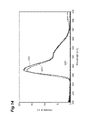
- FIG. 14 is a graph illustrating spectra measured in a fifth example
- FIG. 15 is a graph illustrating spectra obtained by normalizing measured light emission spectra with peak values
- FIGS. 16( a ) and 16 ( b ) are graphs illustrating results of X-ray diffractometry of an amorphous film before and after heat treatment, respectively;
- FIG. 17 is a graph illustrating spectra of ultraviolet light obtained by irradiating a Pr:LuAG film with an electron beam
- FIGS. 18( a ) and 18 ( b ) are SEM photographs concerning a surface of a Pr:LuAG film before and after heat treatment, respectively;
- FIG. 19 is a graph illustrating spectra of ultraviolet light obtained by irradiating Pr:LuAG films with an electron beam
- FIG. 20 is a graph illustrating a spectrum of ultraviolet light obtained by irradiating a Pr:LuAG monocrystalline substrate with an electron beam under the same condition as with a ninth example as a comparative example;
- FIG. 21 is a graph illustrating changes in peak intensity of ultraviolet light occurring when varying the intensity (amperage) of an electron beam
- FIG. 22 is a graph illustrating a relationship between the thickness of a Pr:LuAG polycrystalline film and peak intensity of ultraviolet light
- FIG. 23 is a graph illustrating a relationship between the Pr content in Pr:LuAG-containing materials and peak intensity of ultraviolet light
- FIG. 24 is a graph illustrating spectra measured in a twelfth example
- FIG. 25 is an SEM photograph concerning a surface of a Pr:LuAG polycrystalline film after heat treatment.
- FIG. 26 is a graph illustrating spectra measured in a thirteenth example.
- FIG. 1 is a schematic view illustrating an inner structure of an electron-beam-excited ultraviolet light source 10 in accordance with an embodiment.
- an electron source 12 and an extraction electrode 13 are arranged on the upper end side within a glass envelope (electron tube) 11 evacuated under vacuum.
- an electron beam EB accelerated by a high voltage is emitted from the electron source 12 .
- the electron source 12 one emitting an electron beam having a large area (e.g., cold cathodes such as carbon nanotubes or hot cathodes) can be used.
- a target 20 for ultraviolet light generation is arranged on the lower end side within the envelope 11 .
- the target 20 is set to the ground potential, for example, while a high negative voltage is applied from the power supply part 16 to the electron source 12 .
- the target 20 is irradiated with the electron beam EB emitted from the electron source 12 .
- the target 20 is excited in response to the electron beam EB and generates ultraviolet light UV.
- FIG. 2 is a side view illustrating a structure of the target 20 .
- the target 20 comprises a substrate 21 , a light-emitting layer 22 disposed on the substrate 21 , and an aluminum film 23 .
- the substrate 21 is a planar member made of a material adapted to transmit ultraviolet light therethrough, an example of which is constituted by sapphire (Al 2 O 3 ), silica (SiO 2 ), or rock crystal (crystal of silicon oxide).
- the substrate 21 has a principal surface 21 a and a rear face 21 b .
- a preferred thickness of the substrate 21 is at least 0.1 mm but not more than 10 mm.
- the light-emitting layer 22 is excited in response to the electron beam EB illustrated in FIG. 1 and generates the ultraviolet light UV.
- the light-emitting layer 22 includes a polycrystalline film formed by turning an oxide containing Lu and Si doped with an activator into a polycrystal.
- Preferred examples of such an oxide polycrystal include Lu 2 Si 2 O 7 (LPS) and Lu 2 SiO 5 (LSO) polycrystals doped with a rare-earth element (Pr in an example) serving as an activator.
- LPS Lu 2 Si 2 O 7
- LSO Lu 2 SiO 5
- Different kinds of the oxide crystal (e.g., LPS and LSO) may be mixed.
- a preferred thickness of the polycrystalline film is at least 0.1 ⁇ m but not more than 10 ⁇ m.
- a preferred activator content is at least 0.001 atom % but not more than 10 atom %.
- the light-emitting layer 22 includes a polycrystalline film formed by turning a rare-earth-containing aluminum garnet doped with an activator into a polycrystal.
- Preferred examples of the rare-earth-containing aluminum garnet include Lu 3 Al 5 O 12 (LuAG) and Y 3 Al 5 O 12 (YAG).
- Rare-earth elements are preferred as the activator.
- At least one of scandium (Sc), lanthanum (La), and bismuth (Bi) is preferred as the activator when the rare-earth-containing aluminum garnet crystal is LuAG.
- At least one of Sc and La is preferred as the activator when the rare-earth-containing aluminum garnet crystal is YAG.
- This polycrystalline film has an ultraviolet light emission peak wavelength of 300 ⁇ m or shorter.
- a preferred thickness of the polycrystalline film is at least 0.1 ⁇ m but not more than 10 ⁇ m.
- a preferred activator content is at least 0.001 atom % but not more than 10 atom %.
- FIG. 3 is a chart listing specific examples of the rare-earth-containing aluminum garnet crystal doped with an activator which can be used in the light-emitting layer 22 of this embodiment.
- FIG. 3 illustrates ultraviolet light emission peak wavelengths (unit: nm) corresponding to combinations of activators and base materials.
- examples of the rare-earth-containing aluminum garnet crystal doped with an activator include La:LuAG Sc:LuAG, Bi:LuAG, La:YAG, and Sc:YAG. Their light emission peak wavelengths are not longer than 300 nm and vary depending on the activator content.
- different kinds of rare-earth-containing aluminum garnet crystals e.g., LuAG and YAG
- different kinds of activators e.g., at least two of La, Sc, and Bi
- FIG. 4 is a schematic view illustrating a structure of a laser ablation device 50 used for this manufacturing method.
- the laser ablation device 50 illustrated in FIG. 4 comprises a vacuum container 51 , a sample mount 52 arranged on the bottom face of the vacuum container 51 , and a laser inlet 54 .
- the laser inlet 54 introduces a laser beam B, with which a material 53 is irradiated, into the vacuum container 51 .
- the material 53 is mounted on the sample mount 52 .
- the laser inlet 54 is supplied with a laser beam (having a wavelength of 248 nm) from a KrF excimer laser, for example.
- the laser ablation device 50 further comprises a rotary holder 55 , a heater 56 for heating the substrate 21 , and a gas inlet 57 for feeding an oxygen gas into the vacuum container 51 .
- the rotary holder 55 supports the substrate 21 arranged above the material 53 .
- the rotary holder 55 holds the substrate 21 rotatably about an axis connecting the material 53 and substrate 21 , while exposing the principal surface 21 a of the substrate 21 against the material 53 .
- FIG. 5 is a flowchart illustrating a method for manufacturing the target 20 .
- an amorphous film is vapor-deposited on the substrate 21 (first step S 1 ).
- a ceramic including an oxide containing Lu and Si (e.g., LPS or LSO) and an activator (e.g., Pr) at a predetermined ratio is made as the material 53 at first.
- a ceramic including materials for a rare-earth-containing aluminum garnet crystal (e.g., LuAG or YAG) and an activator (e.g., Sc, La, or Bi) at a predetermined ratio is made as the material 53 (step S 11 ).
- the rare-earth-containing aluminum garnet crystal doped with such an activator has an ultraviolet light emission peak wavelength of 300 nm or shorter.
- the substrate 21 is prepared and installed on the rotary holder 55 of the laser ablation device 50 , while the material 53 made in the step S 11 is mounted on the sample mount 52 (step S 12 ).
- the vacuum container 51 is evacuated (step S 13 ), and the heater 56 heats the substrate 21 to a predetermined temperature (e.g., 800° C.) (step S 14 ).
- the material 53 is irradiated with the laser beam B while feeding the oxygen gas into the vacuum container 51 from the gas inlet 57 (step S 15 ).
- the material 53 evaporates in response to the laser beam B and scatters within the vacuum container 51 .
- a part of the scattered material 53 adheres to the principal surface 21 a of the substrate 21 , thereby forming an amorphous film.
- the amorphous film formed on the principal surface 21 a of the substrate 21 is heat-treated, so as to become a polycrystal (second step S 2 ).
- the substrate 21 having the amorphous film formed thereon is taken out of the laser ablation device 50 and put into a heat treatment furnace (step S 21 ).
- the temperature in the heat treatment furnace is set higher than 1000° C., for example, and this temperature is maintained for a predetermined time, so as to subject the amorphous film on the substrate 21 to heat treatment (annealing) (step S 22 ).
- the heat-treated amorphous film becomes a polycrystal at this time.
- the target 20 in accordance with this embodiment can effectively enhance the ultraviolet light generation efficiency as compared with the case of single crystals. Further, since the above-mentioned polycrystalline film is formed on the ultraviolet-light-transmissive substrate 21 , the target in accordance with this embodiment can suppress the manufacturing cost as compared with the case using the polycrystalline substrate and enhance the transmittance for ultraviolet light.
- the substrate 21 is preferably made of sapphire, silica, or rock crystal as in this embodiment. This enables the substrate 21 to transmit ultraviolet light therethrough and the amorphous film to be heat-treated at high temperature in the step S 22 .
- the polycrystalline film of the light-emitting layer 22 has a thickness of at least 0.1 ⁇ m but not more than 10 ⁇ m as in this embodiment.
- the thickness of the polycrystalline film is preferably at least 0.1 ⁇ m in order for electron beams to contribute to light emission without passing therethrough and preferably 10 ⁇ m or less from the viewpoint of productivity.
- the polycrystalline film having such a thickness can enhance the ultraviolet light emission more effectively.
- the manufacturing method of this embodiment vapor-deposits an amorphous film on the substrate 21 and then heat-treats the amorphous film. While the first step S 1 forms an amorphous film on the substrate 21 , ultraviolet light hardly occurs even when the amorphous film is irradiated with electron beams. By contrast, heat-treating the amorphous film in the second step can turn the amorphous film into a polycrystalline film, whereby a target for ultraviolet light generation which generates ultraviolet light with a high efficiency can be manufactured.
- the first and second steps S 1 and S 2 may be performed concurrently.
- the first to sixth examples to be explained in the following are examples concerning the case where the polycrystalline film of the light-emitting layer 22 is constituted by a Pr:LSO polycrystal.
- the facts found out from these examples seem to be the same in oxide polycrystals containing Lu and Si doped with an activator having the same characteristics as those of the Pr:LSO polycrystal, e.g., Pr:LPS polycrystal.
- an LSO-containing ceramic including 0.5 atom % of Pr was made as the material 53 .
- this Pr:LSO-containing ceramic was mounted on the sample mount 52 of the laser ablation device 50 , while a sapphire substrate having a diameter of 2 inch was installed on the rotary holder 55 .
- the distance between the Pr:LSO-containing ceramic and sapphire substrate was 150 mm.
- the vacuum container 51 was evacuated, and the sapphire substrate was heated to 500° C.
- the material 53 was irradiated with the laser beam B for 120 min, so as to make an amorphous film.
- a KrF excimer laser (150 mJ, 40 Hz) was used as a laser source for the laser beam B. Thereafter, the sapphire substrate was put into a heat treatment furnace, and the sapphire substrate and amorphous film were heated for 2 hr at 1200° C. in a vacuum (10 ⁇ 2 Pa).
- FIG. 6( a ) is a graph illustrating results of X-ray diffractometry of the amorphous film before the heat treatment.
- FIG. 6( b ) is a graph illustrating results of X-ray diffractometry of the film after the heat treatment.
- these graphs While only diffraction lines deriving from Lu 2 O 3 (indicated by crosses in the graph) and those with large half-widths were observed before the heat treatment, diffraction lines deriving from Pr:LSO crystals (indicated by circles in the graph) were observed after the heat treatment. It is seen from these graphs that the amorphous film has been changed into a Pr:LSO polycrystalline film by the heat treatment.
- FIGS. 7( a ) and 7 ( b ) are SEM photographs concerning the surface of the Pr:LSO film before and after the heat treatment, respectively. Referring to FIG. 7( b ), a region subdivided into sections on the order of several micrometers is observed unlike FIG. 7( a ). It is seen from this fact that the amorphous film has been changed into a Pr:LSO polycrystalline film by the heat treatment.
- FIG. 8 is a graph illustrating spectra of ultraviolet light obtained by irradiating the Pr:LSO film with an electron beam.
- graphs G 11 and G 12 represent light emission spectra of the Pr:LSO film after and before the heat treatment, respectively.
- the film before the heat treatment did not emit light.
- the electron beam had an acceleration voltage of 10 kV, an intensity (amperage) of 100 ⁇ A, and a diameter of 2 mm.
- the amorphous film before the heat treatment hardly generated ultraviolet light even when irradiated with the electron beam.
- the polycrystalline Pr:LSO film after the heat treatment favorably generated ultraviolet light upon irradiation with the electron beam.
- the atmosphere at the time of heat treatment which was a vacuum in the first example, was the air.
- the other steps, conditions, and the like are the same as those of the first example.
- results of X-ray diffractometry of the Pr:LSO film made by this example diffraction lines deriving from Pr:LSO crystals were observed as in FIG. 6( b ).
- FIG. 9 is a graph illustrating spectra of ultraviolet light obtained by irradiating the Pr:LSO film with an electron beam.
- graphs G 21 and G 22 represent light emission spectra of the Pr:LSO films made by the first example (heat treatment in a vacuum) and the second example (heat treatment in the air), respectively.
- the electron beam had an acceleration voltage of 10 kV, an intensity (amperage) of 100 ⁇ A, and a diameter of 2 mm. As can be seen from FIG.
- the peak intensity of ultraviolet light generated by irradiation with the electron beam is much higher (i.e., light emission efficiency is much higher) in the Pr:LSO film heat-treated in the air than in the Pr:LSO film heat-treated in a vacuum.
- FIG. 10 is a graph illustrating a spectrum of ultraviolet light obtained by irradiating a Pr:LSO polycrystal-containing substrate with an electron beam under the same condition as with this example as a comparative example.
- graph G 31 represents a light emission spectrum concerning the Pr:LSO polycrystal-containing substrate
- graph G 32 is identical to the graph G 22 of FIG. 9 .
- the peak intensity of ultraviolet light generated by irradiation with the electron beam is much higher (i.e., light emission efficiency is much higher) in the Pr:LSO polycrystalline film than in the Pr:LSO polycrystal-containing substrate.
- the inventors conducted an experiment concerning the relationship between the thickness of the Pr:LSO polycrystalline film and the peak intensity of ultraviolet light. That is, Pr:LSO polycrystalline films were made with various film-forming times, their thicknesses were measured with a step gauge, and then the peak intensity of ultraviolet light generated by irradiating them with an electron beam was measured.
- FIG. 11 is a graph plotting the resulting relationship between the thickness of the Pr:LSO polycrystalline film and the peak intensity of ultraviolet light.
- the thickness of the Pr:LSO polycrystalline film is smaller than a certain value (about 800 nm), the peak intensity of ultraviolet light is higher as the Pr:LSO polycrystalline film is thicker, thereby enhancing the light emission efficiency.
- the thickness of the Pr:LSO polycrystalline film exceeds this value, however, the increase in peak intensity of ultraviolet light is small. It is also seen from this graph that a sufficiently practical ultraviolet light intensity (light emission efficiency) is obtained when the thickness of the Pr:LSO polycrystalline film is 0.1 ⁇ m or greater.
- amorphous films were made by vapor-depositing a material containing Pr:LSO. Two of these amorphous films were heat-treated in a vacuum at temperatures of 1000° C. and 1200° C., respectively, so as to make two Pr:LSO polycrystalline films. The remaining one was not heat-treated.
- the other steps, conditions, and the like are the same as those of the first example.
- Each of thus made three Pr:LSO films was irradiated with an electron beam (with an acceleration voltage of 10 kV and an intensity (amperage) of 100 ⁇ A), and the spectrum of generated ultraviolet light was measured.
- FIG. 12 is a graph illustrating the measured spectra.
- graphs G 40 , G 41 , and G 42 represent the respective cases without heat treatment and with heat treatment at temperatures of 1000° C. and 1200° C.
- FIG. 12 it has been found that the peak intensity of ultraviolet light increases as the heat treatment temperature of the Pr:LSO film rises, thereby yielding higher light emission efficiency.
- FIG. 13 is an SEM photograph concerning the surface of the Pr:LSO polycrystalline film after the heat treatment.
- FIGS. 13( a ), 13 ( b ), and 13 ( c ) illustrate the Pr:LSO film surface in the respective cases without heat treatment and with heat treatment at temperatures of 1000° C. and 1200° C. It is seen from FIG. 13 that the crystallization of Pr:LSO advances as the heat treatment temperature is higher.
- amorphous films were made by vapor-depositing a material containing Pr:LSO. Two of these amorphous films were heat-treated in the air at temperatures of 1200° C. and 1400° C., respectively, so as to make two Pr:LSO polycrystalline films. The remaining one was not heat-treated.
- the other steps, conditions, and the like are the same as those of the first example.
- Each of thus made three Pr:LSO films was irradiated with an electron beam (with an acceleration voltage of 10 kV and an intensity (amperage) of 100 ⁇ A), and the spectrum of generated ultraviolet light was measured.
- FIG. 14 is a graph illustrating the measured spectra.
- graphs G 50 , G 51 , and G 52 represent the respective cases without heat treatment and with heat treatment at temperatures of 1000° C. and 1200° C.
- substantially the same light emission characteristic was obtained whether the heat treatment temperature of the Pr:LSO film was 1200° C. or 1400° C. when the heat treatment was performed in the air.
- the light emission peak intensity in the case where the atmosphere at the time of heat treatment was at the atmospheric pressure was about 1.5 times that in the case where the atmosphere at the time of heat treatment was a vacuum. Therefore, the atmosphere at the time of heat treatment is more preferably at the atmospheric pressure.
- the heat treatment temperature is preferably at least 1000° C. It will be more preferred if the heat treatment temperature is 1200° C. to 1900° C. in particular.
- amorphous films were made by vapor-depositing a material containing Pr:LSO and then heat-treated (for 2 hr) in a heat treatment furnace with a vacuum atmosphere at respective temperatures of 1000° C., 1200° C., 1400° C., and 1500° C., so as to form Pr:LSO polycrystalline films.
- the other steps, conditions, and the like are the same as those of the first example.
- Each of thus made Pr:LSO polycrystalline films was irradiated with an electron beam (with an acceleration voltage of 10 kV and an intensity (amperage) of 100 ⁇ A), and the spectrum of generated ultraviolet light was measured.
- FIG. 15 is a graph illustrating spectra obtained by normalizing the measured spectra with peak values.
- graphs G 61 , G 62 , G 63 , and G 64 represent cases where the heat treatment temperature was 1000° C., 1200° C., 1400° C., and 1500° C., respectively.
- the ultraviolet light emission peak wavelength was 285 nm at the heat treatment temperature of 1000° C., 275 nm at 1200° C., 310 nm and 275 nm at 1400° C., and 310 nm at 1500° C. Since the ultraviolet light emission peak wavelength thus varies depending on the heat treatment temperature, it is preferred for the heat treatment temperature to be set according to the wavelength of ultraviolet light required for the target for ultraviolet light generation.
- the seventh to thirteenth examples to be explained in the following are examples concerning the case where the polycrystalline film of the light-emitting layer 22 is constituted by a Pr:LuAG polycrystal.
- the facts found out from these examples seem to be the same in rare-earth-containing aluminum garnet polycrystals doped with an activator having a composition similar to that of the Pr:LuAG polycrystal, e.g., Sc:LuAG, La:LuAG, Bi:LuAG, Sc:YAG, and La:YAG polycrystals.
- a ceramic containing 0.8 atom % of Pr was made as the material 53 .
- this Pr:LuAG-containing ceramic was mounted on the sample mount 52 of the laser ablation device 50 , while a sapphire substrate having a diameter of 2 inch was installed on the rotary holder 55 .
- the distance between the Pr:LuAG-containing ceramic and sapphire substrate was 150 mm.
- the vacuum container 51 was evacuated, and the sapphire substrate was heated to 1000° C.
- the material 53 was irradiated with the laser beam B for 60 min, so as to make an amorphous film.
- a KrF excimer laser (100 mJ, 100 Hz) was used as a laser light source for the laser beam B. Thereafter, the sapphire substrate was put into a heat treatment furnace, and the sapphire substrate and amorphous film were heated for 2 hr at 1400° C. in the air.
- FIG. 16( a ) is a graph illustrating results of X-ray diffractometry of the amorphous film before the heat treatment.
- FIG. 16( b ) is a graph illustrating results of X-ray diffractometry of the film after the heat treatment.
- diffraction lines deriving from Pr:LuAG crystals indicated by circles in the graph were observed in addition to the former diffraction line after the heat treatment. It is seen from these graphs that the amorphous film has been changed into a Pr:LuAG polycrystal by the heat treatment.
- FIG. 17 is a graph illustrating spectra of ultraviolet light obtained by irradiating the Pr:LuAG film with an electron beam.
- graphs G 71 , G 72 , and G 73 represent light emission spectra of the Pr:LuAG polycrystal as a vapor deposition material (a raw material for laser ablation), the Pr:LuAG film after the heat treatment, and the Pr:LuAG film before the heat treatment, respectively.
- the film before the heat treatment did not emit light.
- the electron beam had an acceleration voltage of 10 kV, an intensity (amperage) of 100 ⁇ A, and a diameter of 2 mm.
- the amorphous film before the heat treatment hardly generated ultraviolet light even when irradiated with the electron beam.
- the polycrystalline Pr:LuAG film after the heat treatment favorably generated ultraviolet light upon irradiation with the electron beam.
- the temperature of the sapphire substrate at the time of forming the Pr:LuAG film which was 1000° C. in the seventh example, was changed to 800° C.
- the heat treatment temperature which was 1400° C. in the seventh example, was changed to 1600° C.
- the other steps, conditions, and the like are the same as those of the seventh example.
- FIGS. 18( a ) and 18 ( b ) are SEM photographs concerning the surface of the Pr:LuAG film before and after the heat treatment, respectively. Referring to FIG. 18( b ), a region subdivided into sections on the order of several micrometers is observed unlike FIG. 18( a ). It is seen from these facts that the amorphous film has been changed into a Pr:LuAG polycrystal by the heat treatment.
- the atmosphere at the time of heat treatment which was the air in the eighth example, was changed to a vacuum (10 ⁇ 2 Pa).
- the other steps, conditions, and the like are the same as those of the eighth example.
- diffraction lines deriving from Pr:LuAG crystals were observed as in FIG. 16( b ).
- FIG. 19 is a graph illustrating spectra of ultraviolet light obtained by irradiating Pr:LuAG films with an electron beam.
- Graphs G 81 and G 82 illustrate light emission spectra of the Pr:LuAG film made by the eighth example (heat treatment in the air) and the Pr:LuAG film made by the ninth example (heat treatment in a vacuum), respectively.
- the electron beam had an acceleration voltage of 10 kV, an intensity (amperage) of 100 ⁇ A, and a diameter of 2 mm. As can be seen from FIG.
- the peak intensity of ultraviolet light generated by irradiation with the electron beam is much higher (i.e., light emission efficiency is much higher) in the Pr:LuAG film heat-treated in a vacuum than in the Pr:LuAG film heat-treated in the air.
- FIG. 20 is a graph illustrating a spectrum of ultraviolet light obtained by irradiating a Pr:LuAG monocrystalline substrate with an electron beam under the same condition as with this example.
- graph G 91 represents a light emission spectrum concerning the Pr:LuAG monocrystalline substrate
- graph G 92 is identical to the graph G 82 of FIG. 19 .
- the peak intensity of ultraviolet light generated by irradiation with the electron beam is much higher (i.e., light emission efficiency is much higher) in the Pr:LuAG polycrystalline thin film than in the Pr:LuAG monocrystalline substrate.
- FIG. 21 is a graph illustrating changes in peak intensity of ultraviolet light occurring when varying the intensity (amperage) of an electron beam.
- graphs G 101 and G 102 represent light emission spectra concerning the Pr:LuAG polycrystalline thin film made by this example and the Pr:LuAG monocrystalline substrate of the comparative example, respectively.
- the intensity of the electron beam and the peak intensity of ultraviolet light have an extremely favorable proportionality (high linearity) therebetween in the Pr:LuAG polycrystalline thin film made by this example.
- the Pr:LuAG polycrystalline thin film made by this example can achieve a peak intensity higher than that of the Pr:LuAG monocrystalline substrate and inhibit the light emission efficiency from dropping even in regions where the electron beam is strong.
- FIG. 22 is a graph plotting the resulting relationship between the thickness of the Pr:LuAG polycrystalline film and the peak intensity of ultraviolet light. Curve G 105 in the graph is a fitted curve.
- the thickness of the Pr:LuAG polycrystalline film is smaller than a certain value (about 500 nm), the peak intensity of ultraviolet light is higher as the Pr:LuAG polycrystalline film is thicker, thereby enhancing the light emission efficiency.
- the thickness of the Pr:LuAG polycrystalline film exceeds this value, however, the peak intensity of ultraviolet light does not increase substantially or decreases instead. It is also seen from this graph that a sufficiently practical ultraviolet light intensity (light emission efficiency) is obtained when the thickness of the Pr:LuAG polycrystalline film is 0.1 ⁇ m or greater.
- FIG. 23 is a graph plotting the resulting relationship between the Pr content in Pr:LuAG-containing materials and the peak intensity of ultraviolet light. Curve G 106 in the graph is a fitted curve.
- the Pr content in Pr:LuAG-containing materials is lower than a certain value (about 0.7 atom %), the peak intensity of ultraviolet light is higher as the Pr content is greater, thereby enhancing the light emission efficiency.
- the Pr content in Pr:LuAG-containing materials exceeds this value, however, the peak intensity of ultraviolet light decreases instead.
- the Pr content in Pr:LuAG-containing materials is preferably at least 0.05 atom % but not more than 2.0 atom %, more preferably at least 0.1 atom % but not more than 1.0 atom %. A sufficiently practical ultraviolet light intensity is seen to be obtained thereby.
- Pr content in Pr:LuAG-containing materials While the relationship between the Pr content in Pr:LuAG-containing materials and the peak intensity of ultraviolet light is explained in this example, the relationship between the Pr content in Pr:LuAG polycrystalline films and the peak intensity of ultraviolet light seems to have a tendency similar to the graph illustrated in FIG. 22 . However, a preferred range of the Pr content in Pr:LuAG polycrystalline films is at least 0.001 atom % but not more than 10 atom %, for example.
- amorphous films were made by vapor-depositing a material containing Pr:LuAG, and these amorphous films were heat-treated in a vacuum at temperatures of 1200° C., 1400° C., 1500° C., 1600° C., 1700° C., 1800° C., and 1900° C., respectively, so as to form Pr:LuAG polycrystalline films.
- the other steps, conditions, and the like are the same as those of the eighth example.
- Each of thus made Pr:LuAG polycrystalline films was irradiated with an electron beam (with an acceleration voltage of 10 kV and an intensity (amperage) of 100 ⁇ A), and the spectrum of generated ultraviolet light was measured.
- FIG. 24 is a graph illustrating the measured spectra.
- graphs G 110 , G 111 , G 112 , G 113 , G 114 , G 115 , and G 116 represent the respective cases with heat treatment at temperatures of 1200° C., 1400° C., 1500° C., 1600° C., 1700° C., 1800° C., and 1900° C.
- the peak intensity of ultraviolet light increases as the heat treatment temperature of the Pr:LuAG film rises, thereby yielding higher light emission efficiency.
- very sharp light emission peaks appear in spectra when the heat treatment temperature is so high as to fall within the range of 1800° C. to 1900° C. No light was emitted when the treatment temperature was 1200° C.
- the heat treatment temperature is preferably 1400° C. to 1800° C. when utilizing wide wavelength regions and 1800° C. to 1900° C. when utilizing light emission peak waveforms.
- FIG. 25 is an SEM photograph concerning the surface of the Pr:LuAG polycrystalline film after the heat treatment.
- FIG. 25 represents SEM photographs in the respective cases with heat treatment at temperatures of 1200° C., 1400° C., 1500° C., 1600° C., 1700° C., 1800° C., and 1900° C. It is seen from FIG. 25 that the crystallization of Pr:LuAG advances as the heat treatment temperature is higher. At 1200° C., the surface of the Pr:LuAG polycrystalline film was seen to be in substantially the same state as the amorphous film before heat treatment illustrated in FIG. 18( a ).
- amorphous films were made by vapor-depositing a material containing Pr:LuAG, and these amorphous films were heat-treated in a heat treatment furnace with the air atmosphere at respective temperatures of 1200° C., 1400° C., 1600° C., and 1700° C., so as to form Pr:LuAG polycrystalline films.
- the other steps, conditions, and the like are the same as those of the eighth example.
- Each of thus made Pr:LuAG polycrystalline films was irradiated with an electron beam (with an acceleration voltage of 10 kV and an intensity (amperage) of 100 ⁇ A), and the spectrum of generated ultraviolet light was measured.
- FIG. 26 is a graph illustrating the measured spectra.
- graphs G 120 , G 121 , G 122 , and G 123 represent the respective cases with heat treatment at temperatures of 1200° C., 1400° C., 1700° C., and 1600° C.
- the heat treatment is performed in the air that the peak intensity of ultraviolet light increases as the heat treatment temperature rises, thereby yielding higher light emission efficiency.
- the light emission efficiency was the highest in the case where the heat treatment temperature was 1600° C. No light was emitted when the treatment temperature was 1200° C. in this case, either.
- the peak intensity (at 310 nm) in the case where the atmosphere at the time of heat treatment was the air was about 2 ⁇ 3 that in the case where the atmosphere at the time of heat treatment was a vacuum.
- the atmosphere at the time of heat treatment is preferably at the atmospheric pressure or lower.
- the atmosphere lower than the atmospheric pressure is more preferably a vacuum (10 ⁇ 2 Pa or lower).
- the heat treatment temperature is preferably at least 1400° C. It will be more preferred if the heat treatment temperature is 1400° C. to 1900° C. in particular.
- the target for ultraviolet light generation, electron-beam-excited ultraviolet light source, and method for manufacturing a target for ultraviolet light generation in accordance with one aspect of the present invention are not limited to the embodiment mentioned above, but can be modified in various ways.
- the polycrystalline film may be made by methods other than such a method.
- the target for ultraviolet light generation, electron-beam-excited ultraviolet light source, and method for manufacturing a target for ultraviolet light generation in accordance with one aspect of the present invention can enhance ultraviolet light generation efficiency.
- 10 electron-beam-excited ultraviolet light source
- 11 envelope
- 12 electron source
- 13 extraction electrode
- 16 power supply part
- 20 target for ultraviolet light generation
- 21 substrate
- 21 a principal surface
- 21 b rear face
- 22 light-emitting layer
- 23 aluminum film
- 50 laser ablation device
- 51 vacuum container
- 52 sample mount
- 53 material
- 54 laser inlet
- 55 rotary holder
- 56 heater
- 57 gas inlet
- B laser beam
- EB electron beam
- UV ultraviolet light.
Applications Claiming Priority (3)
| Application Number | Priority Date | Filing Date | Title |
|---|---|---|---|
| JP2012-233973 | 2012-10-23 | ||
| JP2012233973A JP5580865B2 (ja) | 2012-10-23 | 2012-10-23 | 紫外光発生用ターゲット、電子線励起紫外光源、及び紫外光発生用ターゲットの製造方法 |
| PCT/JP2013/074129 WO2014065028A1 (ja) | 2012-10-23 | 2013-09-06 | 紫外光発生用ターゲット、電子線励起紫外光源、及び紫外光発生用ターゲットの製造方法 |
Publications (2)
| Publication Number | Publication Date |
|---|---|
| US20150294853A1 US20150294853A1 (en) | 2015-10-15 |
| US9240313B2 true US9240313B2 (en) | 2016-01-19 |
Family
ID=50544409
Family Applications (1)
| Application Number | Title | Priority Date | Filing Date |
|---|---|---|---|
| US14/437,376 Expired - Fee Related US9240313B2 (en) | 2012-10-23 | 2013-09-06 | Target for ultraviolet light generation, electron beam-excited ultraviolet light source, and production method for target for ultraviolet light generation |
Country Status (6)
| Country | Link |
|---|---|
| US (1) | US9240313B2 (ja) |
| EP (1) | EP2913378B1 (ja) |
| JP (1) | JP5580865B2 (ja) |
| KR (1) | KR20150079628A (ja) |
| CN (1) | CN104755583B (ja) |
| WO (1) | WO2014065028A1 (ja) |
Cited By (2)
| Publication number | Priority date | Publication date | Assignee | Title |
|---|---|---|---|---|
| US20150270116A1 (en) * | 2012-10-23 | 2015-09-24 | Hamamatsu Photonics K.K. | Target for ultraviolet light generation, electron beam-excited ultraviolet light source, and production method for target for ultraviolet light generation |
| US20150287587A1 (en) * | 2012-10-23 | 2015-10-08 | Hamamatsu Photonics K.K. | Target for ultraviolet light generation, electron beam-excited ultraviolet light source, and production method for target for ultraviolet light generation |
Families Citing this family (8)
| Publication number | Priority date | Publication date | Assignee | Title |
|---|---|---|---|---|
| JP6810938B2 (ja) | 2015-10-29 | 2021-01-13 | 独立行政法人国立高等専門学校機構 | プラズマ殺菌装置 |
| JP6141948B2 (ja) * | 2015-11-30 | 2017-06-07 | 大電株式会社 | 紫外線発光蛍光体、発光素子、及び発光装置 |
| JP6955656B2 (ja) * | 2016-02-15 | 2021-10-27 | 国立大学法人神戸大学 | 紫外発光蛍光体と紫外発光デバイス及び紫外発光蛍光体の作製方法 |
| CN109890940A (zh) * | 2016-10-28 | 2019-06-14 | 大电株式会社 | 紫外线发光荧光体、发光元件和发光装置 |
| SE540283C2 (en) * | 2016-12-08 | 2018-05-22 | Lightlab Sweden Ab | A field emission light source adapted to emit UV light |
| JP6837834B2 (ja) * | 2016-12-28 | 2021-03-03 | 浜松ホトニクス株式会社 | 紫外光発生用ターゲット及びその製造方法、並びに電子線励起紫外光源 |
| JP7030333B2 (ja) * | 2018-04-23 | 2022-03-07 | 国立大学法人神戸大学 | Uvb領域の紫外発光蛍光体および紫外発光デバイス |
| JP7236859B2 (ja) * | 2018-12-17 | 2023-03-10 | 浜松ホトニクス株式会社 | 紫外光発生用ターゲット及びその製造方法、並びに電子線励起紫外光源 |
Citations (14)
| Publication number | Priority date | Publication date | Assignee | Title |
|---|---|---|---|---|
| JPH02225587A (ja) | 1988-10-06 | 1990-09-07 | Schlumberger Overseas Sa | オルト珪酸ルテチウム単結晶シンチレータ検知器 |
| JP2002057388A (ja) | 2000-08-11 | 2002-02-22 | Nippon Avionics Co Ltd | 固体レーザ発振器 |
| WO2006049284A1 (ja) | 2004-11-08 | 2006-05-11 | Tohoku Techno Arch Co., Ltd. | Prを含むシンチレータ用単結晶及びその製造方法並びに放射線検出器及び検査装置 |
| JP2006520836A (ja) | 2003-03-17 | 2006-09-14 | コーニンクレッカ フィリップス エレクトロニクス エヌ ヴィ | 放射源及び蛍光物質を有する照明システム |
| CN1893976A (zh) | 2003-12-17 | 2007-01-10 | 皇家飞利浦电子股份有限公司 | 使用uv发射纳米微粒的放射治疗和医学成像 |
| JP2007077280A (ja) | 2005-09-14 | 2007-03-29 | Ulvac Japan Ltd | 電子線励起発光素子用蛍光体、その作製方法、及び電子線励起発光素子 |
| CN101084329A (zh) | 2004-11-08 | 2007-12-05 | 东北泰克诺亚奇股份有限公司 | 含Pr的闪烁体用单晶及其制造方法和放射线检测器以及检查装置 |
| US20080191607A1 (en) * | 2004-09-03 | 2008-08-14 | Sumitomo Electric Industries, Ltd. | Phosphor, Method For Producing Same, And Light-Emitting Device Using Same |
| JP2008231218A (ja) | 2007-03-20 | 2008-10-02 | Nippon Electric Glass Co Ltd | 蛍光体材料及び白色led |
| JP2010024278A (ja) | 2008-07-16 | 2010-02-04 | Stanley Electric Co Ltd | 蛍光体セラミック板およびそれを用いた発光素子 |
| CN101842869A (zh) | 2007-09-03 | 2010-09-22 | 国立大学法人神户大学 | 深紫外半导体发光装置 |
| JP2010222403A (ja) | 2009-03-19 | 2010-10-07 | Technical Research & Development Institute Ministry Of Defence | レーザーアブレーションを利用した発光膜形成方法及び発光素子 |
| US20120161104A1 (en) * | 2009-08-31 | 2012-06-28 | Ushio Denki Kabushiki Kaisha | Ultraviolet irradiation device |
| JP2012229306A (ja) | 2011-04-25 | 2012-11-22 | Hamamatsu Photonics Kk | 紫外光発生用ターゲット、電子線励起紫外光源、及び紫外光発生用ターゲットの製造方法 |
Family Cites Families (9)
| Publication number | Priority date | Publication date | Assignee | Title |
|---|---|---|---|---|
| US6404127B2 (en) * | 1993-07-20 | 2002-06-11 | University Of Georgia Research Foundation, Inc. | Multi-color microcavity resonant display |
| JP2002033080A (ja) * | 2000-07-14 | 2002-01-31 | Futaba Corp | 紫外線光源 |
| DE10129630A1 (de) * | 2001-06-20 | 2003-01-02 | Philips Corp Intellectual Pty | Niederdruckgasentladungslampe mit Leuchtstoffbeschichtung |
| JP4235748B2 (ja) * | 2002-03-18 | 2009-03-11 | 株式会社日立プラズマパテントライセンシング | 表示装置 |
| DE10238398A1 (de) * | 2002-08-22 | 2004-02-26 | Philips Intellectual Property & Standards Gmbh | Vorrichtung zur Erzeugung von Bildern und/oder Projektionen |
| EP1471128A1 (en) * | 2003-04-24 | 2004-10-27 | Fuji Photo Film Co., Ltd. | Stimulable cerium activated lutetium silicate phosphor |
| JP2006049284A (ja) | 2004-06-29 | 2006-02-16 | Suga Test Instr Co Ltd | 耐候光試験用ランプ |
| JP4883998B2 (ja) * | 2005-12-14 | 2012-02-22 | 秀臣 鯉沼 | 蛍光体とその製造方法 |
| FR2930673A1 (fr) * | 2008-04-28 | 2009-10-30 | Saint Gobain | Lampe plane a emission par effet de champ et sa fabrication |
-
2012
- 2012-10-23 JP JP2012233973A patent/JP5580865B2/ja not_active Expired - Fee Related
-
2013
- 2013-09-06 EP EP13849168.3A patent/EP2913378B1/en not_active Not-in-force
- 2013-09-06 KR KR1020157010428A patent/KR20150079628A/ko not_active Application Discontinuation
- 2013-09-06 WO PCT/JP2013/074129 patent/WO2014065028A1/ja active Application Filing
- 2013-09-06 CN CN201380055517.4A patent/CN104755583B/zh not_active Expired - Fee Related
- 2013-09-06 US US14/437,376 patent/US9240313B2/en not_active Expired - Fee Related
Patent Citations (14)
| Publication number | Priority date | Publication date | Assignee | Title |
|---|---|---|---|---|
| JPH02225587A (ja) | 1988-10-06 | 1990-09-07 | Schlumberger Overseas Sa | オルト珪酸ルテチウム単結晶シンチレータ検知器 |
| JP2002057388A (ja) | 2000-08-11 | 2002-02-22 | Nippon Avionics Co Ltd | 固体レーザ発振器 |
| JP2006520836A (ja) | 2003-03-17 | 2006-09-14 | コーニンクレッカ フィリップス エレクトロニクス エヌ ヴィ | 放射源及び蛍光物質を有する照明システム |
| CN1893976A (zh) | 2003-12-17 | 2007-01-10 | 皇家飞利浦电子股份有限公司 | 使用uv发射纳米微粒的放射治疗和医学成像 |
| US20080191607A1 (en) * | 2004-09-03 | 2008-08-14 | Sumitomo Electric Industries, Ltd. | Phosphor, Method For Producing Same, And Light-Emitting Device Using Same |
| CN101084329A (zh) | 2004-11-08 | 2007-12-05 | 东北泰克诺亚奇股份有限公司 | 含Pr的闪烁体用单晶及其制造方法和放射线检测器以及检查装置 |
| WO2006049284A1 (ja) | 2004-11-08 | 2006-05-11 | Tohoku Techno Arch Co., Ltd. | Prを含むシンチレータ用単結晶及びその製造方法並びに放射線検出器及び検査装置 |
| JP2007077280A (ja) | 2005-09-14 | 2007-03-29 | Ulvac Japan Ltd | 電子線励起発光素子用蛍光体、その作製方法、及び電子線励起発光素子 |
| JP2008231218A (ja) | 2007-03-20 | 2008-10-02 | Nippon Electric Glass Co Ltd | 蛍光体材料及び白色led |
| CN101842869A (zh) | 2007-09-03 | 2010-09-22 | 国立大学法人神户大学 | 深紫外半导体发光装置 |
| JP2010024278A (ja) | 2008-07-16 | 2010-02-04 | Stanley Electric Co Ltd | 蛍光体セラミック板およびそれを用いた発光素子 |
| JP2010222403A (ja) | 2009-03-19 | 2010-10-07 | Technical Research & Development Institute Ministry Of Defence | レーザーアブレーションを利用した発光膜形成方法及び発光素子 |
| US20120161104A1 (en) * | 2009-08-31 | 2012-06-28 | Ushio Denki Kabushiki Kaisha | Ultraviolet irradiation device |
| JP2012229306A (ja) | 2011-04-25 | 2012-11-22 | Hamamatsu Photonics Kk | 紫外光発生用ターゲット、電子線励起紫外光源、及び紫外光発生用ターゲットの製造方法 |
Non-Patent Citations (3)
| Title |
|---|
| International Preliminary Report on Patentability mailed May 7, 2015 for PCT/JP2013/074129. |
| L. Pidol et al., "Scintillation properties of Lu2Si2O7:Ce3+, a fast and efficient scintillator crystal", J. Phys.: Condens. Matter 15, 2003, p. 2091-p. 2102. |
| Zorenko, Y., et al., "Luminescence Centers in Y3Al5O12:La Single Crystals," Journal of Phyiscs: Conference Series, vol. 289, No. 1, Oct. 30, 2011, pp. 1-7. |
Cited By (4)
| Publication number | Priority date | Publication date | Assignee | Title |
|---|---|---|---|---|
| US20150270116A1 (en) * | 2012-10-23 | 2015-09-24 | Hamamatsu Photonics K.K. | Target for ultraviolet light generation, electron beam-excited ultraviolet light source, and production method for target for ultraviolet light generation |
| US20150287587A1 (en) * | 2012-10-23 | 2015-10-08 | Hamamatsu Photonics K.K. | Target for ultraviolet light generation, electron beam-excited ultraviolet light source, and production method for target for ultraviolet light generation |
| US9728393B2 (en) * | 2012-10-23 | 2017-08-08 | Hamamatsu Photonics K.K. | Target for ultraviolet light generation, electron beam-excited ultraviolet light source, and production method for target for ultraviolet light generation |
| US9852898B2 (en) * | 2012-10-23 | 2017-12-26 | Hamamatsu Photonics K.K. | Target for ultraviolet light generation, electron beam-excited ultraviolet light source, and production method for target for ultraviolet light generation |
Also Published As
| Publication number | Publication date |
|---|---|
| KR20150079628A (ko) | 2015-07-08 |
| JP5580865B2 (ja) | 2014-08-27 |
| CN104755583A (zh) | 2015-07-01 |
| US20150294853A1 (en) | 2015-10-15 |
| WO2014065028A1 (ja) | 2014-05-01 |
| CN104755583B (zh) | 2017-05-17 |
| EP2913378A4 (en) | 2016-09-14 |
| EP2913378B1 (en) | 2017-10-11 |
| JP2014086255A (ja) | 2014-05-12 |
| EP2913378A1 (en) | 2015-09-02 |
Similar Documents
| Publication | Publication Date | Title |
|---|---|---|
| US9240313B2 (en) | Target for ultraviolet light generation, electron beam-excited ultraviolet light source, and production method for target for ultraviolet light generation | |
| US9728393B2 (en) | Target for ultraviolet light generation, electron beam-excited ultraviolet light source, and production method for target for ultraviolet light generation | |
| US8895947B2 (en) | Ultraviolet light generating target, electron-beam-excited ultraviolet light source, and method for producing ultraviolet light generating target | |
| EP2703471B1 (en) | Ultraviolet light generating target, electron-beam-excited ultraviolet light source, and method for producing ultraviolet light generating target | |
| US9852898B2 (en) | Target for ultraviolet light generation, electron beam-excited ultraviolet light source, and production method for target for ultraviolet light generation | |
| US11887837B2 (en) | Ultraviolet light generation target, method for manufacturing ultraviolet light generation target, and electron-beam-excited ultraviolet light source | |
| CN108257848B (zh) | 紫外光产生用靶及其制造方法以及电子束激发紫外光源 | |
| CN107615442A (zh) | 紫外光产生用靶及其制造方法 |
Legal Events
| Date | Code | Title | Description |
|---|---|---|---|
| AS | Assignment |
Owner name: HAMAMATSU PHOTONICS K.K., JAPAN Free format text: ASSIGNMENT OF ASSIGNORS INTEREST;ASSIGNORS:HONDA, YOSHINORI;TAKETOMI, HIROYUKI;FUKUYO, FUMITSUGU;AND OTHERS;SIGNING DATES FROM 20150428 TO 20150430;REEL/FRAME:035628/0828 |
|
| STCF | Information on status: patent grant |
Free format text: PATENTED CASE |
|
| CC | Certificate of correction | ||
| MAFP | Maintenance fee payment |
Free format text: PAYMENT OF MAINTENANCE FEE, 4TH YEAR, LARGE ENTITY (ORIGINAL EVENT CODE: M1551); ENTITY STATUS OF PATENT OWNER: LARGE ENTITY Year of fee payment: 4 |
|
| FEPP | Fee payment procedure |
Free format text: MAINTENANCE FEE REMINDER MAILED (ORIGINAL EVENT CODE: REM.); ENTITY STATUS OF PATENT OWNER: LARGE ENTITY |
|
| LAPS | Lapse for failure to pay maintenance fees |
Free format text: PATENT EXPIRED FOR FAILURE TO PAY MAINTENANCE FEES (ORIGINAL EVENT CODE: EXP.); ENTITY STATUS OF PATENT OWNER: LARGE ENTITY |
|
| STCH | Information on status: patent discontinuation |
Free format text: PATENT EXPIRED DUE TO NONPAYMENT OF MAINTENANCE FEES UNDER 37 CFR 1.362 |
|
| FP | Lapsed due to failure to pay maintenance fee |
Effective date: 20240119 |