US9123725B2 - Semiconductor device having fuse pattern - Google Patents
Semiconductor device having fuse pattern Download PDFInfo
- Publication number
- US9123725B2 US9123725B2 US14/088,654 US201314088654A US9123725B2 US 9123725 B2 US9123725 B2 US 9123725B2 US 201314088654 A US201314088654 A US 201314088654A US 9123725 B2 US9123725 B2 US 9123725B2
- Authority
- US
- United States
- Prior art keywords
- fuse pattern
- fuse
- pattern
- semiconductor device
- insulation layer
- Prior art date
- Legal status (The legal status is an assumption and is not a legal conclusion. Google has not performed a legal analysis and makes no representation as to the accuracy of the status listed.)
- Active, expires
Links
- 239000004065 semiconductor Substances 0.000 title claims abstract description 114
- 238000009413 insulation Methods 0.000 claims abstract description 109
- 239000000758 substrate Substances 0.000 claims abstract description 32
- 239000011810 insulating material Substances 0.000 claims description 80
- 229910052751 metal Inorganic materials 0.000 claims description 63
- 239000002184 metal Substances 0.000 claims description 63
- 125000006850 spacer group Chemical group 0.000 claims description 41
- 239000002245 particle Substances 0.000 claims description 30
- 239000000463 material Substances 0.000 claims description 11
- 230000008439 repair process Effects 0.000 abstract description 7
- 238000009791 electrochemical migration reaction Methods 0.000 abstract description 6
- 230000004888 barrier function Effects 0.000 description 10
- 238000000034 method Methods 0.000 description 7
- 238000010586 diagram Methods 0.000 description 6
- 230000010365 information processing Effects 0.000 description 6
- 230000008569 process Effects 0.000 description 6
- 238000004891 communication Methods 0.000 description 5
- 239000004020 conductor Substances 0.000 description 5
- 230000002950 deficient Effects 0.000 description 5
- 238000004519 manufacturing process Methods 0.000 description 5
- 150000004767 nitrides Chemical class 0.000 description 5
- 229910052782 aluminium Inorganic materials 0.000 description 4
- XAGFODPZIPBFFR-UHFFFAOYSA-N aluminium Chemical compound [Al] XAGFODPZIPBFFR-UHFFFAOYSA-N 0.000 description 4
- 239000010949 copper Substances 0.000 description 4
- 238000012360 testing method Methods 0.000 description 4
- 239000004642 Polyimide Substances 0.000 description 3
- 229920001721 polyimide Polymers 0.000 description 3
- RYGMFSIKBFXOCR-UHFFFAOYSA-N Copper Chemical compound [Cu] RYGMFSIKBFXOCR-UHFFFAOYSA-N 0.000 description 2
- XUIMIQQOPSSXEZ-UHFFFAOYSA-N Silicon Chemical compound [Si] XUIMIQQOPSSXEZ-UHFFFAOYSA-N 0.000 description 2
- 230000008901 benefit Effects 0.000 description 2
- 229910052802 copper Inorganic materials 0.000 description 2
- 229920006336 epoxy molding compound Polymers 0.000 description 2
- 229910052710 silicon Inorganic materials 0.000 description 2
- 239000010703 silicon Substances 0.000 description 2
- WFKWXMTUELFFGS-UHFFFAOYSA-N tungsten Chemical compound [W] WFKWXMTUELFFGS-UHFFFAOYSA-N 0.000 description 2
- 229910052721 tungsten Inorganic materials 0.000 description 2
- 239000010937 tungsten Substances 0.000 description 2
- JBRZTFJDHDCESZ-UHFFFAOYSA-N AsGa Chemical compound [As]#[Ga] JBRZTFJDHDCESZ-UHFFFAOYSA-N 0.000 description 1
- 229910001218 Gallium arsenide Inorganic materials 0.000 description 1
- 229910000673 Indium arsenide Inorganic materials 0.000 description 1
- GPXJNWSHGFTCBW-UHFFFAOYSA-N Indium phosphide Chemical compound [In]#P GPXJNWSHGFTCBW-UHFFFAOYSA-N 0.000 description 1
- 229910000577 Silicon-germanium Inorganic materials 0.000 description 1
- ATJFFYVFTNAWJD-UHFFFAOYSA-N Tin Chemical compound [Sn] ATJFFYVFTNAWJD-UHFFFAOYSA-N 0.000 description 1
- LEVVHYCKPQWKOP-UHFFFAOYSA-N [Si].[Ge] Chemical compound [Si].[Ge] LEVVHYCKPQWKOP-UHFFFAOYSA-N 0.000 description 1
- 239000000853 adhesive Substances 0.000 description 1
- 230000001070 adhesive effect Effects 0.000 description 1
- 239000012861 aquazol Substances 0.000 description 1
- 229920006187 aquazol Polymers 0.000 description 1
- 239000005380 borophosphosilicate glass Substances 0.000 description 1
- 239000003990 capacitor Substances 0.000 description 1
- 230000001413 cellular effect Effects 0.000 description 1
- 238000012937 correction Methods 0.000 description 1
- 230000008878 coupling Effects 0.000 description 1
- 238000010168 coupling process Methods 0.000 description 1
- 238000005859 coupling reaction Methods 0.000 description 1
- 238000001312 dry etching Methods 0.000 description 1
- 238000005516 engineering process Methods 0.000 description 1
- 230000009969 flowable effect Effects 0.000 description 1
- VTGARNNDLOTBET-UHFFFAOYSA-N gallium antimonide Chemical compound [Sb]#[Ga] VTGARNNDLOTBET-UHFFFAOYSA-N 0.000 description 1
- WPYVAWXEWQSOGY-UHFFFAOYSA-N indium antimonide Chemical compound [Sb]#[In] WPYVAWXEWQSOGY-UHFFFAOYSA-N 0.000 description 1
- RPQDHPTXJYYUPQ-UHFFFAOYSA-N indium arsenide Chemical compound [In]#[As] RPQDHPTXJYYUPQ-UHFFFAOYSA-N 0.000 description 1
- 239000012212 insulator Substances 0.000 description 1
- 239000007769 metal material Substances 0.000 description 1
- 238000010295 mobile communication Methods 0.000 description 1
- 238000012986 modification Methods 0.000 description 1
- 230000004048 modification Effects 0.000 description 1
- 229910052759 nickel Inorganic materials 0.000 description 1
- 230000002093 peripheral effect Effects 0.000 description 1
- 239000011148 porous material Substances 0.000 description 1
- 230000002265 prevention Effects 0.000 description 1
- 238000012545 processing Methods 0.000 description 1
- 229910052707 ruthenium Inorganic materials 0.000 description 1
- 238000000926 separation method Methods 0.000 description 1
- 229910021332 silicide Inorganic materials 0.000 description 1
- FVBUAEGBCNSCDD-UHFFFAOYSA-N silicide(4-) Chemical compound [Si-4] FVBUAEGBCNSCDD-UHFFFAOYSA-N 0.000 description 1
- 239000007787 solid Substances 0.000 description 1
- 239000011343 solid material Substances 0.000 description 1
- OCGWQDWYSQAFTO-UHFFFAOYSA-N tellanylidenelead Chemical compound [Pb]=[Te] OCGWQDWYSQAFTO-UHFFFAOYSA-N 0.000 description 1
- 238000001039 wet etching Methods 0.000 description 1
Images


Classifications
-
- G—PHYSICS
- G06—COMPUTING; CALCULATING OR COUNTING
- G06F—ELECTRIC DIGITAL DATA PROCESSING
- G06F12/00—Accessing, addressing or allocating within memory systems or architectures
- G06F12/02—Addressing or allocation; Relocation
-
- H—ELECTRICITY
- H01—ELECTRIC ELEMENTS
- H01L—SEMICONDUCTOR DEVICES NOT COVERED BY CLASS H10
- H01L23/00—Details of semiconductor or other solid state devices
- H01L23/52—Arrangements for conducting electric current within the device in operation from one component to another, i.e. interconnections, e.g. wires, lead frames
- H01L23/522—Arrangements for conducting electric current within the device in operation from one component to another, i.e. interconnections, e.g. wires, lead frames including external interconnections consisting of a multilayer structure of conductive and insulating layers inseparably formed on the semiconductor body
- H01L23/525—Arrangements for conducting electric current within the device in operation from one component to another, i.e. interconnections, e.g. wires, lead frames including external interconnections consisting of a multilayer structure of conductive and insulating layers inseparably formed on the semiconductor body with adaptable interconnections
- H01L23/5256—Arrangements for conducting electric current within the device in operation from one component to another, i.e. interconnections, e.g. wires, lead frames including external interconnections consisting of a multilayer structure of conductive and insulating layers inseparably formed on the semiconductor body with adaptable interconnections comprising fuses, i.e. connections having their state changed from conductive to non-conductive
-
- G—PHYSICS
- G06—COMPUTING; CALCULATING OR COUNTING
- G06F—ELECTRIC DIGITAL DATA PROCESSING
- G06F12/00—Accessing, addressing or allocating within memory systems or architectures
- G06F12/02—Addressing or allocation; Relocation
- G06F12/0223—User address space allocation, e.g. contiguous or non contiguous base addressing
- G06F12/023—Free address space management
- G06F12/0238—Memory management in non-volatile memory, e.g. resistive RAM or ferroelectric memory
- G06F12/0246—Memory management in non-volatile memory, e.g. resistive RAM or ferroelectric memory in block erasable memory, e.g. flash memory
-
- G—PHYSICS
- G06—COMPUTING; CALCULATING OR COUNTING
- G06F—ELECTRIC DIGITAL DATA PROCESSING
- G06F13/00—Interconnection of, or transfer of information or other signals between, memories, input/output devices or central processing units
- G06F13/14—Handling requests for interconnection or transfer
-
- H—ELECTRICITY
- H01—ELECTRIC ELEMENTS
- H01L—SEMICONDUCTOR DEVICES NOT COVERED BY CLASS H10
- H01L23/00—Details of semiconductor or other solid state devices
- H01L23/52—Arrangements for conducting electric current within the device in operation from one component to another, i.e. interconnections, e.g. wires, lead frames
- H01L23/522—Arrangements for conducting electric current within the device in operation from one component to another, i.e. interconnections, e.g. wires, lead frames including external interconnections consisting of a multilayer structure of conductive and insulating layers inseparably formed on the semiconductor body
- H01L23/532—Arrangements for conducting electric current within the device in operation from one component to another, i.e. interconnections, e.g. wires, lead frames including external interconnections consisting of a multilayer structure of conductive and insulating layers inseparably formed on the semiconductor body characterised by the materials
- H01L23/5329—Insulating materials
-
- H—ELECTRICITY
- H10—SEMICONDUCTOR DEVICES; ELECTRIC SOLID-STATE DEVICES NOT OTHERWISE PROVIDED FOR
- H10B—ELECTRONIC MEMORY DEVICES
- H10B20/00—Read-only memory [ROM] devices
- H10B20/20—Programmable ROM [PROM] devices comprising field-effect components
- H10B20/25—One-time programmable ROM [OTPROM] devices, e.g. using electrically-fusible links
-
- H—ELECTRICITY
- H01—ELECTRIC ELEMENTS
- H01L—SEMICONDUCTOR DEVICES NOT COVERED BY CLASS H10
- H01L2924/00—Indexing scheme for arrangements or methods for connecting or disconnecting semiconductor or solid-state bodies as covered by H01L24/00
-
- H—ELECTRICITY
- H01—ELECTRIC ELEMENTS
- H01L—SEMICONDUCTOR DEVICES NOT COVERED BY CLASS H10
- H01L2924/00—Indexing scheme for arrangements or methods for connecting or disconnecting semiconductor or solid-state bodies as covered by H01L24/00
- H01L2924/0001—Technical content checked by a classifier
- H01L2924/0002—Not covered by any one of groups H01L24/00, H01L24/00 and H01L2224/00
Definitions
- the present invention relates to a semiconductor device.
- a semiconductor device may be manufactured through several procedures performed in a sequence, including a fabrication process, an electrical die sorting (EDS) process, an assembly process and a test process.
- the EDS typically includes a pre-laser test in which semiconductor chips are inspected, a repair process in which defective semiconductor chip confirmed in the pre-laser test are replaced with redundancy semiconductor chips, and a post-laser test in which the replaced normal semiconductor chips are inspected.
- the repair process is a process of switching a path of an electrical signal by cutting a fuse.
- a defective cell that does not operate normally is replaced with a redundant cell or a defective circuit is replaced with a normal circuit.
- the repair process is often comprised of cutting a fuse connected to a defective cell and replacing the defective cell with a redundant normal cell.
- the present disclosure provides a semiconductor device having improved reliability by preventing a fuse cut through a repair process from being electrically reconnected by electrochemical migration.
- a semiconductor device includes a substrate, a fuse including first fuse pattern and a second fuse pattern formed at the same level on the substrate, the first fuse pattern and the second fuse pattern being spaced a first width apart from each other such that a gap in the fuse is disposed at a first location between the first fuse pattern and the second fuse pattern, and a first insulation layer formed on the first fuse pattern and the second fuse pattern, the first insulation layer including an opening above the first location and having a second width smaller than the first width.
- a semiconductor device including a substrate, a first fuse pattern and a second fuse pattern formed on the substrate, the first fuse pattern and the second fuse pattern being spaced a first width apart from each other, a first insulation layer formed on the first fuse pattern and the second fuse pattern, the first insulation layer including an opening formed between the first fuse pattern and the second fuse pattern, an insulating material formed between the first fuse pattern and the second fuse pattern, and an air gap formed between the first fuse pattern and the insulating material.
- a semiconductor device including a substrate, a fuse including a first fuse pattern and a second fuse pattern formed on the substrate, the first fuse pattern and the second fuse pattern being spaced a first width apart from each other, and an insulation layer formed on the first fuse pattern and the second fuse pattern, the insulation layer including an opening formed between the first fuse pattern and the second fuse pattern, wherein at least one of the first fuse pattern and the second fuse pattern is undercut below the insulation layer.
- a semiconductor device includes a substrate; a first fuse pattern of a fuse and a second fuse pattern of the fuse, formed on the substrate at a same plane, the first fuse pattern and the second fuse pattern being spaced a first width apart from each other; and an insulative pattern formed between and at the same plane as the first fuse pattern and second fuse pattern.
- the insulative pattern includes at least a first portion formed of a solid material, and at least a second portion that does not permit electrochemical migration of conductive material between the first fuse pattern and the second fuse pattern.
- FIG. 1 is a view illustrating a semiconductor device according to a first exemplary embodiment
- FIG. 2 is a view illustrating the semiconductor device shown in FIG. 1 after being assembled, according to one exemplary embodiment
- FIG. 3 is a view illustrating a semiconductor device according to an additional exemplary embodiment
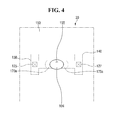
- FIG. 4 is a plan view of FIG. 3 , according to one exemplary embodiment
- FIG. 5 is a view illustrating the semiconductor device shown in FIG. 3 after being assembled, according to one exemplary embodiment
- FIG. 6 is a view illustrating the semiconductor device shown in FIG. 3 , further comprising a pad, according to one exemplary embodiment
- FIG. 7 is a view illustrating a semiconductor device according to another exemplary embodiment
- FIG. 8 is a view illustrating the semiconductor device shown in FIG. 7 after being assembled, according to one exemplary embodiment
- FIG. 9 is a view illustrating a semiconductor device according to a further exemplary embodiment.
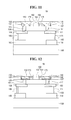
- FIG. 10 is a view illustrating the semiconductor device shown in FIG. 9 after being assembled, according to one exemplary embodiment
- FIG. 11 is a view illustrating a semiconductor device according to another exemplary embodiment
- FIG. 12 is a view illustrating the semiconductor device shown in FIG. 11 after being assembled, according to one exemplary embodiment
- FIG. 13 is a view illustrating a semiconductor device according to another exemplary embodiment
- FIG. 14 is a plan view of FIG. 13 , according to one exemplary embodiment
- FIG. 15 is a view illustrating the semiconductor device shown in FIG. 13 after being assembled, according to one exemplary embodiment
- FIG. 16 is a block diagram illustrating one example of a memory card including semiconductor devices according to certain exemplary embodiments
- FIG. 17 is a block diagram illustrating an information processing system including semiconductor devices according to certain exemplary embodiments.
- FIG. 18 is a block diagram of an electronic device including semiconductor devices according to certain exemplary embodiments.
- Embodiments described herein will be described referring to plan views and/or cross-sectional views by way of ideal schematic views. Accordingly, the exemplary views may be modified depending on manufacturing technologies and/or tolerances. Therefore, the disclosed embodiments are not limited to those shown in the views, but include modifications in configuration formed on the basis of manufacturing processes. Therefore, regions exemplified in figures have schematic properties, and shapes of regions shown in figures exemplify specific shapes of regions of elements, and the specific properties and shapes do not limit aspects of the invention.
- spatially relative terms such as “beneath,” “below,” “lower,” “above,” “upper” and the like, may be used herein for ease of description to describe one element's or feature's relationship to another element(s) or feature(s) as illustrated in the figures. It will be understood that the spatially relative terms are intended to encompass different orientations of the device in use or operation in addition to the orientation depicted in the figures. For example, if the device in the figures is turned over, elements described as “below” or “beneath” other elements or features would then be oriented “above” the other elements or features. Thus, the term “below” can encompass both an orientation of above and below. The device may be otherwise oriented (rotated 90 degrees or at other orientations) and the spatially relative descriptors used herein interpreted accordingly.
- FIGS. 1 and 2 a semiconductor device according to one exemplary embodiment will be described with reference to FIGS. 1 and 2 .
- FIG. 1 is a view illustrating a semiconductor device according to an exemplary embodiment
- FIG. 2 is an exemplary view illustrating the semiconductor device shown in FIG. 1 after being assembled.
- a semiconductor device 10 includes a substrate 100 , a first fuse pattern 130 , a second fuse pattern 140 and a first insulation layer 150 .
- the substrate 100 may be bulk silicon or a silicon-on-insulator (SOI).
- the substrate 100 may be a silicon substrate or may include other materials, such as silicon germanium, indium antimonide, lead telluride, indium arsenide, indium phosphide, gallium arsenide or gallium antimonide, but not limited thereto.
- a first circuit pattern 105 and a second circuit pattern 110 may be formed on the substrate 100 .
- the first circuit pattern 105 and the second circuit pattern 110 may be formed on, for example, a cell region, but not limited thereto.
- the first and second circuit patterns 105 and 110 may include a transistor, a diode, a capacitor, etc., respectively.
- the first and second circuit patterns 105 and 110 may constitute circuit devices. Therefore, the semiconductor device 10 may be a semiconductor chip incorporating a plurality of circuit devices.
- the circuit devices may include a plurality of memory devices.
- the memory devices may include, for example, a volatile semiconductor memory device and a nonvolatile semiconductor memory device.
- the volatile semiconductor memory device may include, for example, DRAM, SRAM, and so on.
- the nonvolatile semiconductor memory device may include, for example, EPROM, EEPROM, Flash EEPROM, and so on.
- the first and second circuit patterns 105 and 110 are formed on the substrate 100 , but aspects of the present disclosure are not limited thereto.
- the first and second circuit patterns 105 and 110 may also be buried in the substrate 100 .
- the second insulation layer 102 may be formed on the substrate 100 and may cover the first and second circuit patterns 105 and 110 .
- a first metal wiring 120 and a second metal wiring 122 may be formed within the second insulation layer 102 .
- the first metal wiring 120 may be electrically connected to the first circuit pattern 105 through a first connection wiring 106
- the second metal wiring 122 may be electrically connected to the second circuit pattern 110 through a second connection wiring 111 .
- the second insulation layer 102 may include, for example, oxide, nitride, oxynitride, or a low dielectric constant (low-k) material.
- the low dielectric constant material may include, for example, FOX, TOSZ, USG, BSG, PSG, BPSG, PRTEOS, FSG, HDP, PEOX, FCVD, and combinations thereof.
- the first metal wiring 120 and the second metal wiring 122 may include, for example, a metal, such as aluminum (Al).
- a third insulation layer 104 may be formed on the first metal wiring 120 and the second metal wiring 122 .
- the third insulation layer 104 may include, for example, oxide, nitride, oxynitride, or a low-k material.
- the first fuse pattern 130 and the second fuse pattern 140 may be formed on the third insulation layer 104 .
- the first fuse pattern 130 and second fuse pattern 140 may be part of a fuse.
- the first fuse pattern 130 and second fuse pattern 140 may form a cut fuse, which may also be described as a repair fuse.
- the first fuse pattern 130 and the second fuse pattern 140 may be formed in a fourth insulation layer 107 formed on the third insulation layer 104 .
- the third insulation layer 104 and the fourth insulation layer 107 may be formed at the same level.
- the first fuse pattern 130 and the second fuse pattern 140 may be spaced apart from each other.
- the first fuse pattern 130 and the second fuse pattern 140 are spaced a first width w 1 apart from each other.
- the different fuse patterns 130 and 140 may have originally been part of a conductive line extending in a lengthwise direction, wherein a part of the line was cut to form the two different fuse patterns (see, for example, FIG. 4 .
- the first fuse pattern 130 and the second fuse pattern 140 may include, for example, at least one of aluminum (Al) and copper (Cu), but aspects of the present disclosure are not limited thereto.
- the first fuse pattern 130 and the second fuse pattern 140 may be formed at the same level within the semiconductor device 10 . For layers formed at the level, a layer (or a component) formed on a predetermined region and a layer (or a component) formed on another region may be formed by the same fabricating process.
- the fourth insulation layer 107 may include, for example, oxide, nitride, oxynitride, or a low-k material.
- a first metal wiring 120 and a second metal wiring 122 may be positioned below the first fuse pattern 130 and the second fuse pattern 140 .
- the first fuse pattern 130 may be electrically connected to the first metal wiring 120 through a first via 125
- the second fuse pattern 140 may be electrically connected to the second metal wiring 122 through a second via 127 . Therefore, the first fuse pattern 130 and the second fuse pattern 140 may be electrically connected to the first circuit pattern 105 and the second circuit pattern 110 , respectively.
- the first via 125 and the second via 127 may be formed in the third insulation layer 104 while passing through the third insulation layer 104 .
- the first via 125 and the second via 127 may include, for example, at least one of aluminum (Al), copper (Cu) and tungsten (W).
- a barrier metal (not shown) may be interposed between each of the first via 125 and the second via 127 and the third insulation layer 104 , but aspects of the present disclosure are not limited thereto.
- a first barrier metal layer 132 and a second barrier metal layer 142 may further be formed between the third insulation layer 104 and the first fuse pattern 130 and between the third insulation layer 104 and the second fuse pattern 140 , respectively.
- the first barrier metal layer 132 and the second barrier metal layer 142 may be formed in contact with the first fuse pattern 130 and the second fuse pattern 140 , respectively.
- the first barrier metal layer 132 and the second barrier metal layer 142 may prevent the respective materials included in the first fuse pattern 130 and the second fuse pattern 140 from being diffused into the third insulation layer 104 .
- the first barrier metal layer 132 and the second barrier metal layer 142 may be formed at the same level, and may include, for example, Ta, TaN, Ti, TiN, Ru, Co, Ni, NiB, and WN.
- the first insulation layer 150 may be formed on the first fuse pattern 130 and the second fuse pattern 140 .
- the first insulation layer 150 may include an opening 155 .
- the opening 155 formed in the first insulation layer 150 may have a second width w 2 .
- the first insulation layer 150 may include, for example, oxide, nitride, or oxynitride, but aspects of the present disclosure are not limited thereto.
- the opening 155 may be formed between the first fuse pattern 130 and the second fuse pattern 140 .
- the second width w 2 of the opening 155 is smaller than the first width w 1 , such that the width of the opening 155 is smaller than the gap between the first fuse pattern 130 and the second fuse pattern 140 . Since the gap between the first fuse pattern 130 and the second fuse pattern 140 is greater than the width of the opening 155 , the opening 155 may not overlap at least one of the first fuse pattern 130 and the second fuse pattern 140 .
- at least one of the first fuse pattern 130 and the second fuse pattern 140 may be undercut below the first insulation layer 150 .
- An undercut region formed below the first insulation layer 150 may be formed by, for example, wet etching, dry etching, or a combination thereof.
- the first insulation 150 may overhang the first fuse pattern 130 and/or the second fuse pattern 140 .
- the opening 155 does not overlap the first fuse pattern 130 , and lateral surfaces of the second fuse pattern 140 and a first insulating layer 130 that defines the opening 155 are coplanar.
- FIG. 2 illustrates an adhesive for facilitating adhesion to another semiconductor device is formed on the first insulation layer 150 to assemble the semiconductor device 10 shown in FIG. 1 .
- FIG. 1 illustrates that a fuse is repaired before the semiconductor device 10 is assembled
- FIG. 2 illustrates a state of the semiconductor device 10 including a repaired fuse after it is assembled with another semiconductor device.
- the semiconductor device 10 may further include an insulating material 160 . At least a portion of the insulating material 160 may be formed between the first fuse pattern 130 and the second fuse pattern 140 . Since the insulating material 160 is formed between the first fuse pattern 130 and the second fuse pattern 140 , an air gap 170 may be formed between the first fuse pattern 130 and the insulating material 160 and/or between the second fuse pattern 140 and the insulating material 160 .
- the insulating material 160 may include a first portion 162 and a second portion 164 .
- the first portion 162 of the insulating material 160 may pass through the opening 155 to extend up to the third insulation layer 104 and may be formed between the first fuse pattern 130 and the second fuse pattern 140 .
- the second portion 164 of the insulating material 160 may be connected to the first portion 162 of the insulating material 160 and may be formed on the first insulation layer 150 .
- the insulating material 160 may include, for example, a die attach film (DAF) or an epoxy molding compound (EMC), but aspects of the present invention are not limited thereto.
- DAF die attach film
- EMC epoxy molding compound
- the insulating material 160 is spatially separated from the first fuse pattern 130 , and is formed in contact with the second fuse pattern 140 .
- the first portion 162 of the insulating material 160 may be positioned between the first fuse pattern 130 and the second fuse pattern 140 while making contact with the second fuse pattern 140 . Since the insulating material 160 is spatially separated from the first fuse pattern 130 , a first air gap 170 is formed between the first portion 162 of the insulating material 160 and the first fuse pattern 130 . However, since the first portion 162 of the insulating material 160 and the second fuse pattern 140 make contact with each other, an air gap is not formed between the first portion 162 of the insulating material 160 and the second fuse pattern 140 .
- an insulative pattern is formed on the same plane as the fuse patterns 130 and 140 and between the fuse patterns 130 and 140 .
- the insulative pattern may include, as described above, an air portion and a solid portion (e.g., insulating material 162 ). At least the air portion may prevent electrochemical migration of material from the first fuse pattern 130 to the second fuse pattern 140 .
- the insulative pattern may include additional portions, such as an additional air portion, as described in more detail in connection with the embodiments discussed below.
- FIG. 2 illustrates that a conductive material is not included in the first portion 162 of the insulating material 160 , but aspects of the present disclosure are not limited thereto.
- the insulating material 160 may be a porous material.
- the material included in the second fuse pattern 140 may be diffused into the insulating material 160 by electrochemical migration when the semiconductor device 10 is exposed to high-temperature and high-humidity conditions.
- a line-shaped conductive band may be formed in the first portion 162 of the insulating material 160 .
- the first air gap 170 is formed between the first portion 162 of the insulating material 160 and the first fuse pattern 130 , the conductive material included in the first portion 162 of the insulating material 160 is not connected to the first fuse pattern 130 .
- the first air gap 170 is formed between the first portion 162 of the insulating material 160 and the first fuse pattern 130 , thereby electrically insulating the first fuse pattern 130 and the second fuse pattern 140 and physically preventing a conductive band such as described above from being formed. Therefore, since the first fuse pattern 130 and the second fuse pattern 140 are electrically insulated by the first air gap 170 , the reliability of a semiconductor package manufactured using the semiconductor device 10 can be improved.
- the insulating material 160 is not depicted as being inserted into the undercut region of the first fuse pattern 130 formed below the first insulation layer 150 .
- aspects of the present disclosure are not limited thereto.
- a portion of the insulating material 160 may be inserted into the undercut region of the first fuse pattern 130 formed below the first insulation layer 150 .
- the first air gap 170 is formed between the insulating material 160 and the first fuse pattern 130 .
- FIGS. 3 to 6 a semiconductor device according to another embodiment will be described with reference to FIGS. 3 to 6 .
- This embodiment is substantially the same as the previous embodiment, except that a second fuse pattern may be additionally undercut.
- the same functional components as those of the first embodiment are denoted by the same reference numerals and repeated explanations thereof will be briefly given or will not be given.
- FIG. 3 is a view illustrating a semiconductor device according to a second embodiment of the present invention
- FIG. 4 is a plan view of FIG. 3
- FIG. 5 is a view illustrating the semiconductor device shown in FIG. 3 after being assembled
- FIG. 6 is a view illustrating the semiconductor device shown in FIG. 3 , further comprising a pad.
- an exemplary semiconductor device 20 includes a substrate 100 , a first fuse pattern 130 , a second fuse pattern 140 and a first insulation layer 150 .
- the first circuit pattern 105 and the second circuit pattern 110 are formed on the substrate 100 .
- a first metal wiring 120 and a second metal wiring 122 electrically connected to the first circuit pattern 105 and the second circuit pattern 110 are formed on the first circuit pattern 105 and the second circuit pattern 110 , respectively.
- the first metal wiring 120 and the second metal wiring 122 may be formed within the second insulation layer 102 formed on the substrate 100 .
- the first fuse pattern 130 and the second fuse pattern 140 are formed on the first metal wiring 120 and the second metal wiring 122 .
- the first fuse pattern 130 and the second fuse pattern 140 are electrically connected to the first metal wiring 120 and the second metal wiring 122 , respectively.
- a first via 125 is formed between the first fuse pattern 130 and the first metal wiring 120
- a second via 127 is formed between the second fuse pattern 140 and the second metal wiring 122 .
- the first via 125 and the second via 127 may be formed in the third insulation layer 104 interposed between each of the first fuse pattern 130 and the second fuse pattern 140 and the second insulation layer 102 .
- the first insulation layer 150 is formed on the first fuse pattern 130 and the second fuse pattern 140 , and includes an opening 155 formed between the first fuse pattern 130 and the second fuse pattern 140 .
- the second width w 2 of the opening 155 is smaller than the first width w 1 .
- the gap between the first fuse pattern 130 and the second fuse pattern 140 is greater than the width of the opening 155 , and the opening 155 overlaps both the first fuse pattern 130 and the second fuse pattern 140 .
- the first fuse pattern 130 and the second fuse pattern 140 are undercut below the first insulation layer 150 .
- opening 155 does not overlap the first fuse pattern 130 or the second fuse pattern 140 .
- the first insulation layer 150 overhangs both the first fuse pattern 130 and the second fuse pattern 140 .
- FIGS. 1 and 2 depict the first fuse pattern 130 and the second fuse pattern 140 below the first insulation layer 150 having the same width, but aspects of the present disclosure are not limited thereto.
- the width of the first fuse pattern 130 below the first insulation layer 150 may be different from the width of the second fuse pattern 140 below the first insulation layer 150 .
- the opening 155 is formed in the first insulation layer 150 .
- the third insulation layer 104 positioned below the first insulation layer 150 may be exposed by the opening 155 .
- a pair of the first fuse pattern 130 and the second fuse pattern 140 may be positioned below the first insulation layer 150 .
- Neither the first fuse pattern 130 nor the second fuse pattern 140 overlap the opening 155 .
- Each fuse pattern 130 and 140 may be recessed from an edge of the opening 155 .
- An undercut region 170 a of the first fuse pattern 130 (e.g., region where the first fuse pattern 130 is missing) is positioned between the opening 155 and the first fuse pattern 130
- an undercut region 175 a of the second fuse pattern 140 (e.g., region where the second fuse pattern 140 is missing) is positioned between the opening 155 and the second fuse pattern 140 .
- the two undercut regions may correspond to a cut portion of a fuse that lies beneath the first insulation layer 150 .
- first fuse pattern 130 and the second fuse pattern 140 are shown in the illustrated embodiment, but aspects of the present invention are not limited thereto.
- the first fuse pattern 130 and the second fuse pattern 140 are aligned in one direction, but aspects of the present invention are not limited thereto.
- a fuse that has yet to be repaired (e.g., an unbroken fuse) is exemplified as a dog-bone shaped fuse in the illustrated embodiment, but aspects of the present invention are not limited thereto.
- the fuse that has yet to be repaired may have a linear shape or another shape different from the dog-bone shape or the linear shape.
- the semiconductor device 20 may further include an insulating material 160 .
- the insulating material 160 includes a first portion 162 and a second portion 164 .
- the first portion 162 of the insulating material 160 passes through the opening 155 and is formed between the first fuse pattern 130 and the second fuse pattern 140 , and the second portion 164 of the insulating material 160 may be formed on the first insulation layer 150 . Since the insulating material 160 is formed between the first fuse pattern 130 and the second fuse pattern 140 , air gaps 170 and 175 may be formed between the first fuse pattern 130 and the insulating material 160 and/or between the second fuse pattern 140 and the insulating material 160 .
- the first air gap 170 is formed between the first fuse pattern 130 and the insulating material 160
- the second air gap 175 is formed between the second fuse pattern 140 and the insulating material 160 .
- the width of the first fuse pattern 130 undercut below the first insulation layer 150 and that of the second fuse pattern 140 undercut below the first insulation layer 150 are different from each other, and the portion of the insulating material 160 is inserted into the undercut portion of the first fuse pattern 130 or the second fuse pattern 140 , only one of the first air gap 170 and the second air gap 175 may be formed, or if both air gaps are still formed, the first air gap 170 and second air gap 175 may have different widths.
- the first portion 162 of the insulating material 160 is spatially separated from the first fuse pattern 130 and the second fuse pattern 140 .
- the first air gap 170 is formed between the first fuse pattern 130 and the first portion 162 of the insulating material 160
- the second air gap 175 is formed between the second fuse pattern 140 and the first portion 162 of the insulating material 160 .
- the first air gap 170 is surrounded by the first fuse pattern 130 , the first insulation layer 150 , the insulating material 160 , the third insulation layer 104 and the fourth insulation layer 107
- the second air gap 175 is surrounded by the second fuse pattern 140 , the first insulation layer 150 , the insulating material 160 , the third insulation layer 104 and the fourth insulation layer 107 .
- the first air gap 170 and the second air gap 175 are formed between the first fuse pattern 130 and the second fuse pattern 140 , and the first fuse pattern 130 and the second fuse pattern 140 may be electrically and electrochemically insulated. Therefore, even when the semiconductor device 20 is exposed to high-temperature and high-humidity conditions, since the first air gap 170 and the second air gap 175 are formed between the first fuse pattern 130 and the second fuse pattern 140 , the first fuse pattern 130 and the second fuse pattern 140 remain electrically separated due to the air gaps' prevention of electrochemical migration of conductive material from the first fuse pattern 130 to the second fuse pattern 140 .
- a pad 135 for transferring electrical signals to the first circuit pattern 105 , the second circuit pattern 110 , the first metal wiring and the second metal wiring 122 may be formed on the first insulation layer 150 positioned on the substrate of a cell region and a peripheral circuit region.
- the pad 135 may be formed using a conductive material such as a metal, conductive metal nitride or metal silicide.
- the pad 135 may be formed of a metal having low specific resistance, such as aluminum (Al) or tungsten (W).
- Al aluminum
- W tungsten
- the pad 135 may not be formed immediately above the first fuse pattern 130 and the second fuse pattern 140 . In detail, the pad 135 is not formed immediately above the opening 155 , and may be horizontally separate from the opening 155 .
- the opening 155 may be an open region of the semiconductor device 20 , and a conductive pattern is not formed immediately above the opening 155 .
- FIGS. 7 and 8 A semiconductor device according to an additional embodiment will be described with reference to FIGS. 7 and 8 .
- the embodiment shown in FIGS. 7 and 8 is substantially the same as the previous embodiment, except that a third insulation layer includes a trench.
- the same functional components as those of the previous embodiment are denoted by the same reference numerals and repeated explanations thereof will be briefly given or will not be given.
- FIG. 7 is a view illustrating a semiconductor device according to a third exemplary embodiment of the present disclosure and FIG. 8 is a view illustrating the semiconductor device shown in FIG. 7 after being assembled.
- a semiconductor device 30 includes a first fuse pattern 130 , a second fuse pattern 140 , a trench 104 t and a first insulation layer 150 .
- the first insulation layer 150 including an opening 155 is formed on the first fuse pattern 130 and the second fuse pattern 140 .
- the opening 155 is formed between the first fuse pattern 130 and the second fuse pattern 140 and does not overlap at least one of the first fuse pattern 130 and the second fuse pattern 140 . Therefore, the first insulation layer 150 overhangs at least one of the first fuse pattern 130 and the second fuse pattern 140 .
- the third insulation layer 104 positioned under the first fuse pattern 130 and the second fuse pattern 140 includes the trench 104 t .
- the trench 104 t is formed within the third insulation layer 104 . At least a portion of the trench 104 t may overlap the opening 155 included in the first insulation layer 150 .
- the trench 104 t may be formed between the first fuse pattern 130 and the second fuse pattern 140 and in one embodiment, does not overlap the first fuse pattern 130 or the second fuse pattern 140 . As such, in the embodiment shown in FIG. 7 , the first fuse pattern 130 and the second fuse pattern 140 do not protrude above the trench 104 t .
- a gap between the first fuse pattern 130 and the second fuse pattern 140 is equal to a width of the trench 104 t.
- the width of the trench 104 t and the width of the opening 155 are equal to each other, and the trench 104 t entirely overlaps the opening 155 , but aspects of the present invention are not limited thereto.
- the trench 104 t is provided for the purpose of more definitely ensuring spatial and electrical separation between the first fuse pattern 130 and the second fuse pattern 140 , and width of the trench 104 t may vary.
- the trench 104 t since the trench 104 t may be formed using the opening 155 as a window, it may entirely overlap the opening 155 . However, an overlapping extent of the trench 104 t and the opening 155 may vary.
- the semiconductor device 30 may further include an insulating material 160 having a first portion 162 and a second portion 164 .
- the first portion 162 of the insulating material 160 may pass through the opening 155 and may extend up to the inside of the trench 104 t formed between the first fuse pattern 130 and the second fuse pattern 140 .
- the insulating material 160 may fill the trench 104 t formed in the third insulation layer 104 .
- a first air gap 170 is formed between the first fuse pattern 130 and the first portion 162 of the insulating material 160
- a second air gap 175 is formed between the second fuse pattern 140 and the first portion 162 of the insulating material 160 .
- the air gap 170 and the second air gap 175 may be positioned farther from the substrate 100 than the bottom surface of the trench 104 t is from the substrate. If the width of the trench 104 t is greater than that of the opening 155 , a portion of at least one of the first air gap 170 and the second air gap 175 may be formed in the third insulation layer 104 .
- FIGS. 9 and 10 A semiconductor device according to a further embodiment is be described with reference to FIGS. 9 and 10 .
- This embodiment is substantially the same as the embodiment shown in FIG. 3 , except that the illustrated semiconductor device includes a conductive particle.
- the same functional components as those of the embodiment of FIG. 3 are denoted by the same reference numerals and repeated explanations thereof will be briefly given or will not be given.
- FIG. 9 is a view illustrating an exemplary semiconductor device and FIG. 10 is a view illustrating the semiconductor device shown in FIG. 9 after being assembled.
- a semiconductor device 40 includes a first fuse pattern 130 , a second fuse pattern 140 , a conductive particle 180 and a first insulation layer 150 .
- the first fuse pattern 130 and the second fuse pattern 140 electrically connected to the first circuit pattern 105 and the second circuit pattern 110 are formed on the third insulation layer 104 .
- the first insulation layer 150 including an opening 155 is formed on the first fuse pattern 130 and the second fuse pattern 140 .
- the opening 155 is formed between the first fuse pattern 130 and the second fuse pattern 140 .
- At least one of the first fuse pattern 130 and the second fuse pattern 140 is undercut below the first insulation layer 150 .
- the conductive particle 180 is formed between the first fuse pattern 130 and the second fuse pattern 140 .
- the conductive particle 180 is formed on the third insulation layer 104 .
- the conductive particle 180 may be formed in contact with the third insulation layer 104 .
- the conductive particle 180 may entirely overlap the opening 155 .
- the conductive particle 180 is spatially spaced apart from the first fuse pattern 130 and the second fuse pattern 140 , but aspects of the present invention are not limited thereto.
- the conductive particle 180 may be connected to one of the first fuse pattern 130 and the second fuse pattern 140 .
- the fuse pattern is not connected to the conductive particle 180 and is undercut below the first insulation layer 150 .
- the fuse pattern is spatially spaced apart from the conductive particle 180 .
- the conductive particle 180 may be an externally applied metallic material.
- the conductive particle 180 may include, for example, materials included in the fuse patterns 130 and 140 , or materials included in barrier metal layers 132 and 142 .
- the conductive particle 180 may be a residue produced when the first fuse pattern 130 and the second fuse pattern 140 are formed by repairing (e.g., cutting) a fuse connecting the first circuit pattern 105 and the second circuit pattern 110 .
- the conductive particle 180 does not protrude from a top surface of the first insulation layer 150 , but aspects of the present invention are not limited thereto. For example, a portion of the conductive particle 180 may protrude from the top surface of the first insulation layer 150 .
- the semiconductor device 40 may further include an insulating material 160 having a first portion 162 and a second portion 164 .
- the first portion 162 of the insulating material 160 formed between the first fuse pattern 130 and the second fuse pattern 140 while passing through an opening 155 , may surround the conductive particle 180 .
- the first air gap 170 is formed between the first fuse pattern 130 and the first portion 162 of the insulating material 160
- the second air gap 175 is formed between the second fuse pattern 140 and the first portion 162 of the insulating material 160 by the insulating material 160 surrounding the conductive particle 180 .
- the first air gap 170 may be formed between the first fuse pattern 130 and the conductive particle 180
- the second air gap 175 may be formed between the second fuse pattern 140 and the conductive particle 180 .
- the conductive particle 180 is completely surrounded by the insulating material 160 .
- aspects of the present disclosure are not limited thereto.
- a portion of the conductive particle 180 may be exposed by the insulating material 160 .
- the first and second air gaps 170 and 175 are formed between the conductive particle 180 and each of the first and second fuse patterns 130 and 140 .
- the first air gap 170 and the second air gap 175 are formed on both side surfaces of the conductive particle 180 .
- aspects of the present disclosure are not limited thereto.
- the semiconductor device 40 may include the first and second air gaps 170 and 175 formed between the first fuse pattern 130 and the conductive particle 180 and/or between the second fuse pattern 140 and the conductive particle 180 .
- FIGS. 11 and 12 A semiconductor device according to another embodiment is be described with reference to FIGS. 11 and 12 .
- This is substantially the same as the embodiment shown in FIG. 3 , except that the illustrated semiconductor device includes a spacer.
- the same functional components as those of the embodiment shown in FIG. 3 are denoted by the same reference numerals and repeated explanations thereof will be briefly given or will not be given.
- FIG. 11 is a view illustrating an exemplary semiconductor device and FIG. 12 is a view illustrating the semiconductor device shown in FIG. 11 after being assembled.
- a semiconductor device 50 includes a first fuse pattern 130 , a second fuse pattern 140 , a first spacer 190 , a second spacer 195 and a first insulation layer 150 .
- the first fuse pattern 130 and the second fuse pattern 140 electrically connected to a first circuit pattern 105 and a second circuit pattern 110 , respectively, are formed on a third insulation layer 104 .
- the first insulation layer 150 including an opening 155 is formed on the first fuse pattern 130 and the second fuse pattern 140 .
- the opening 155 is formed between the first fuse pattern 130 and the second fuse pattern 140 .
- At least one of the first fuse pattern 130 and the second fuse pattern 140 is undercut below the first insulation layer 150 .
- a first spacer 190 is formed between the first fuse pattern 130 and the opening 155
- a second spacer 195 is formed between the second fuse pattern 140 and the opening 155 .
- the first spacer 190 may be disposed in a space formed when the first fuse pattern 130 is undercut below the first insulation layer 150
- the second spacer 195 may be disposed in a space formed when the second fuse pattern 140 is undercut below the first insulation layer 150 .
- first spacer 190 and the second spacer 195 may be formed between the third insulation layer 104 and the first insulation layer 150 .
- a first air gap 170 may be formed between the first spacer 190 and the first fuse pattern 130
- a second air gap 175 may be formed between the second spacer 195 and the second fuse pattern 140 .
- the first air gap 170 and the second air gap 175 are formed, but aspects of the present disclosure are not limited thereto.
- the semiconductor device 50 including the first spacer 190 and the second spacer 195 , may include only one of the first air gap 170 and the second air gap 175 formed below the first insulation layer 150 , or may include both.
- first spacer 190 and the second spacer 195 may include, for example, an insulating material.
- first spacer 190 and the second spacer 195 may include photosensitive polyimide (PSPI), polyimide (PI), photosensitive polyhydroxystyrene, and so on, but aspects of the present disclosure are not limited thereto.
- PSPI photosensitive polyimide
- PI polyimide
- photosensitive polyhydroxystyrene and so on, but aspects of the present disclosure are not limited thereto.
- the first spacer 190 and the second spacer 195 may be formed by hardening a flowable insulating material.
- the semiconductor device 50 may further include an insulating material 160 having a first portion 162 and a second portion 164 .
- the first portion 162 of the insulating material 160 may pass through the opening 155 to be formed between the first spacer 190 and the second spacer 195 .
- the first spacer 190 and the second spacer 195 are formed in contact with the insulating material 160 .
- the first spacer 190 may be formed between the first fuse pattern 130 and the insulating material 160
- the second spacer 195 may be formed between the second fuse pattern 140 and the insulating material 160 . Since at least one of the first spacer 190 and the second spacer 195 is formed, the spacers may be formed between the first fuse pattern 130 and the insulating material 160 and/or between the second fuse pattern 140 and the insulating material 160 .
- the first air gap 170 is formed between the first fuse pattern 130 and the first portion 162 of the insulating material 160
- the second air gap 175 is formed between the second fuse pattern 140 and the first portion 162 of the insulating material 160 .
- the first air gap 170 is formed between the first fuse pattern 130 and the first spacer 190
- the second air gap 175 is formed between the second fuse pattern 140 and the second spacer 195 .
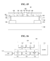
- a semiconductor device according to a further embodiment is described with reference to FIGS. 13 to 15 .
- FIG. 13 is a view illustrating a semiconductor device according to an exemplary embodiment
- FIG. 14 is a plan view of FIG. 13
- FIG. 15 is a view illustrating the semiconductor device shown in FIG. 13 after being assembled.
- a semiconductor device 60 includes a substrate 100 , a first metal wiring 120 , a second metal wiring 122 , a first fuse pattern 130 , a second fuse pattern 140 and a first insulation layer 150 .
- a first circuit pattern 105 and a second circuit pattern 110 may be formed on the substrate 100 .
- a first metal wiring 120 and a second metal wiring 122 may be formed on the second insulation layer 102 and may be electrically connected to the first circuit pattern 105 and the second circuit pattern 110 , respectively.
- the first fuse pattern 130 and the second fuse pattern 140 are formed on the second insulation layer 102 and are electrically connected to the first metal wiring 120 and the second metal wiring 122 , respectively.
- the first metal wiring 120 , the second metal wiring 122 , the first fuse pattern 130 and the second fuse pattern 140 are all formed on the second insulation layer 102 .
- first metal wiring 120 , the second metal wiring 122 , the first fuse pattern 130 and the second fuse pattern 140 may be equally spaced apart (e.g., in a vertical direction) from the substrate 100 to then be formed on the second insulation layer 102 , which is different from cases of the embodiments discussed previously.
- first and second fuse patterns 130 and 140 and the first and second metal wirings 120 and 122 are spaced different distances apart from the substrate 100 .
- the first and second fuse patterns 130 and 140 and the first and second metal wirings 120 and 122 are equally spaced apart from the substrate 100 .
- the first insulation layer 150 is formed on the first and second metal wirings 120 and 122 and the first and second fuse patterns 130 and 140 .
- the first insulation layer 150 includes an opening 155 formed between the first fuse pattern 130 and the second fuse pattern 140 . Relationships between various functional components of the semiconductor device 60 , the opening 155 and the fuse patterns 130 and 140 are substantially the same with those of the previous embodiments, and descriptions thereof will be omitted.
- the first fuse pattern 130 and the first metal wiring 120 are connected to each other, and the second fuse pattern 140 and the second metal wiring 122 are connected to each other.
- the opening 155 formed in the first insulation layer 150 is positioned between the first fuse pattern 130 and the second fuse pattern 140 .
- An undercut region 170 a of the first fuse pattern 130 is positioned between the opening 155 and the first fuse pattern 130
- an undercut region 175 a of the second fuse pattern 140 is positioned between the opening 155 and the second fuse pattern 140 .
- the first fuse pattern 130 is directly connected to the first metal wiring 120 and the second fuse pattern 140 is directly connected to the second metal wiring 122 .
- the disclosure is not limited thereto.
- the semiconductor device 60 may further include an insulating material 160 having a first portion 162 and a second portion 164 .
- the insulating material 160 is formed between the first fuse pattern 130 and the second fuse pattern 140 .
- a first air gap 170 is formed between the first fuse pattern 130 and the insulating material 160
- a second air gap 175 is formed between the second fuse pattern 140 and the insulating material 160 .
- FIG. 16 is a block diagram illustrating one example of a memory card including semiconductor devices according to exemplary embodiments.
- a memory including semiconductor devices may be employed in a memory card 1200 .
- the memory card 1200 may include a memory controller 1220 for general data exchange between a host and the memory 1210 .
- the SRAM 1221 may be used as an operating memory of a central processing unit (CPU) 1222 .
- a host interface (I/F) 1223 includes a data exchange protocol of a host connected to the memory card 1200 .
- An error correction code (ECC) 1224 detects and corrects an error included in data read from the memory 1210 .
- a memory interface (I/F) 1225 may interface with the memory 1210 , which may employ one or more of the various embodiments described in connection with FIGS. 1-15 .
- the CPU 1222 performs general control operations for data exchange of the memory controller 1220 .
- FIG. 17 is a block diagram illustrating an information processing system including semiconductor devices according to exemplary embodiments.
- the information processing system 1300 may include a memory system 1310 having semiconductor devices according to various embodiments described above.
- the information processing system 1300 may include a memory system 1310 , a modem 1320 CPU 1330 , RAM 1340 , and a user interface 1350 , electrically connected to a system bus 1360 .
- the memory system 1310 may include a memory 1311 and a memory controller 1312 and may have substantially the same configuration as the memory card 1200 shown in FIG. 16 .
- the memory system 1310 stores data processed by the CPU 1330 or data inputted from the exterior.
- the information processing system 1300 may be applied to a memory card, SSD, a camera image processor (CIS), and other various application chipsets.
- the memory system 1310 may be configured to be applied to SSD. In this case, the information processing system 1300 can stably and reliably store high capacity data.
- FIG. 18 is a block diagram of an electronic device including semiconductor devices according to certain exemplary embodiments.
- an electronic device 1400 may include semiconductor devices according to various embodiments described above.
- the electronic device 1400 may be used in a wireless communication system (e.g., a personal digital assistant (PDA), a notebook computer, a portable computer, a web tablet, a wireless phone, or a digital music system) or various information transmitting/receiving systems in wireless communication surroundings.
- a wireless communication system e.g., a personal digital assistant (PDA), a notebook computer, a portable computer, a web tablet, a wireless phone, or a digital music system
- PDA personal digital assistant
- the electronic device 1400 may include a controller 1410 , an input/output (I/O) device 1420 , a memory 1430 , and a wireless interface 1440 .
- the memory 1430 may include semiconductor devices according to various embodiments described above.
- the controller 1410 may include a microprocessor, a digital signal processor, or the like.
- the memory 1430 may be used in storing commands (or user data) processed by the controller 1410 .
- the wireless interface 1440 may be used in transmitting/receiving data through a wireless a communication network.
- the wireless interface 1440 may be coupled to the network via a wired or wireless coupling.
- the wireless interface 1440 may include an antenna or a wired/wireless transceiver.
- the electronic device 1400 may use a communication interface protocol, for example, for third generation communication systems, e.g., Code Division Multiple Access (CDMA), Global System for Mobile Communications (GSM), North American Digital Cellular (NADC), Extended-Time Division Multiple Access (E-TDMA), Wideband Code Division Multiple Access (WCDMA), and CDMA2000.
- CDMA Code Division Multiple Access
- GSM Global System for Mobile Communications
- NADC North American Digital Cellular
- E-TDMA Extended-Time Division Multiple Access
- WCDMA Wideband Code Division Multiple Access
- CDMA2000 Code Division Multiple Access
- CDMA Code Division Multiple Access
- GSM Global System for Mobile Communications
- NADC North American Digital Cellular
- E-TDMA Extended-Time Division Multiple Access
- WCDMA Wideband Code Division Multiple Access
- CDMA2000 Code Division Multiple Access 2000
Landscapes
- Engineering & Computer Science (AREA)
- Physics & Mathematics (AREA)
- General Physics & Mathematics (AREA)
- Theoretical Computer Science (AREA)
- Power Engineering (AREA)
- Microelectronics & Electronic Packaging (AREA)
- Computer Hardware Design (AREA)
- Condensed Matter Physics & Semiconductors (AREA)
- General Engineering & Computer Science (AREA)
- Techniques For Improving Reliability Of Storages (AREA)
- Design And Manufacture Of Integrated Circuits (AREA)
- Read Only Memory (AREA)
- Semiconductor Integrated Circuits (AREA)
Priority Applications (1)
| Application Number | Priority Date | Filing Date | Title |
|---|---|---|---|
| US14/798,474 US9449918B2 (en) | 2012-12-04 | 2015-07-14 | Semiconductor device having fuse pattern |
Applications Claiming Priority (2)
| Application Number | Priority Date | Filing Date | Title |
|---|---|---|---|
| KR1020120139675A KR102002826B1 (ko) | 2012-12-04 | 2012-12-04 | 저장 장치, 플래시 메모리 및 저장 장치의 동작 방법 |
| KR10-2012-0139675 | 2012-12-04 |
Related Child Applications (1)
| Application Number | Title | Priority Date | Filing Date |
|---|---|---|---|
| US14/798,474 Division US9449918B2 (en) | 2012-12-04 | 2015-07-14 | Semiconductor device having fuse pattern |
Publications (2)
| Publication Number | Publication Date |
|---|---|
| US20140151845A1 US20140151845A1 (en) | 2014-06-05 |
| US9123725B2 true US9123725B2 (en) | 2015-09-01 |
Family
ID=50023364
Family Applications (3)
| Application Number | Title | Priority Date | Filing Date |
|---|---|---|---|
| US14/088,654 Active 2033-12-07 US9123725B2 (en) | 2012-12-04 | 2013-11-25 | Semiconductor device having fuse pattern |
| US14/095,240 Active 2034-09-30 US9589888B2 (en) | 2012-12-04 | 2013-12-03 | Storage devices, flash memories, and methods of operating storage devices |
| US14/798,474 Expired - Fee Related US9449918B2 (en) | 2012-12-04 | 2015-07-14 | Semiconductor device having fuse pattern |
Family Applications After (2)
| Application Number | Title | Priority Date | Filing Date |
|---|---|---|---|
| US14/095,240 Active 2034-09-30 US9589888B2 (en) | 2012-12-04 | 2013-12-03 | Storage devices, flash memories, and methods of operating storage devices |
| US14/798,474 Expired - Fee Related US9449918B2 (en) | 2012-12-04 | 2015-07-14 | Semiconductor device having fuse pattern |
Country Status (5)
| Country | Link |
|---|---|
| US (3) | US9123725B2 (zh) |
| EP (1) | EP2759935B1 (zh) |
| JP (1) | JP6487142B2 (zh) |
| KR (1) | KR102002826B1 (zh) |
| CN (1) | CN103853503B (zh) |
Cited By (2)
| Publication number | Priority date | Publication date | Assignee | Title |
|---|---|---|---|---|
| US10398791B2 (en) | 2013-10-18 | 2019-09-03 | Deutsches Krebsforschungszentrum | Labeled inhibitors of prostate specific membrane antigen (PSMA), their use as imaging agents and pharmaceutical agents for the treatment of prostate cancer |
| US10649692B2 (en) | 2016-07-29 | 2020-05-12 | Samsung Electronics Co., Ltd. | Storage device, system including the same and method of operating the same |
Families Citing this family (7)
| Publication number | Priority date | Publication date | Assignee | Title |
|---|---|---|---|---|
| KR20160074237A (ko) * | 2014-12-18 | 2016-06-28 | 에스케이하이닉스 주식회사 | 데이터 저장 장치 및 그것의 동작 방법 |
| CN104503707B (zh) | 2014-12-24 | 2018-03-06 | 华为技术有限公司 | 读取数据的方法以及装置 |
| US9933950B2 (en) * | 2015-01-16 | 2018-04-03 | Sandisk Technologies Llc | Storage operation interrupt |
| KR102413755B1 (ko) * | 2015-11-20 | 2022-06-28 | 삼성전자주식회사 | 리텐션 특성에 의한 성능 저하를 복구하는 저장 장치의 동작 방법 및 이를 포함하는 데이터 처리 시스템의 동작 방법 |
| KR102650994B1 (ko) * | 2016-10-14 | 2024-03-26 | 삼성전자주식회사 | 메모리 장치 |
| KR102450313B1 (ko) * | 2020-09-23 | 2022-10-04 | 주식회사 유라코퍼레이션 | 연성 인쇄 회로 기판 및 그의 제조 방법 |
| KR102513122B1 (ko) * | 2020-09-23 | 2023-03-23 | 주식회사 유라코퍼레이션 | 연성 인쇄 회로 기판의 설치 구조 |
Citations (18)
| Publication number | Priority date | Publication date | Assignee | Title |
|---|---|---|---|---|
| KR940000919A (ko) | 1992-06-30 | 1994-01-10 | 하기주 | 감광성 수지 필름 |
| JPH10256373A (ja) | 1997-03-07 | 1998-09-25 | Seiko Epson Corp | 半導体装置及び半導体装置の製造方法 |
| JPH1187522A (ja) | 1997-07-11 | 1999-03-30 | Sony Corp | 半導体装置の製造方法 |
| KR20010059452A (ko) | 1999-12-30 | 2001-07-06 | 박종섭 | 퓨즈 박스 형성 방법 |
| KR20020002770A (ko) | 2000-06-30 | 2002-01-10 | 박종섭 | 반도체 소자의 제조방법 |
| US6563188B2 (en) | 2001-08-08 | 2003-05-13 | Mitsubishi Denki Kabushiki Kaisha | Semiconductor device having multilayer passivation layer formed over memory cell fuse area |
| US6638795B2 (en) | 2001-07-02 | 2003-10-28 | Fujitsu Limited | Semiconductor device and method of fabricating the same |
| US6720591B2 (en) | 2001-04-23 | 2004-04-13 | Renesas Technology Corp. | Semiconductor integrated circuit device |
| KR20050096377A (ko) | 2004-03-30 | 2005-10-06 | 주식회사 하이닉스반도체 | 퓨즈와 퓨즈 박스를 갖는 반도체 장치의 제조 방법 |
| KR20070014818A (ko) | 2005-07-29 | 2007-02-01 | 삼성전자주식회사 | 반도체 메모리 소자의 리페어 방법 |
| US20090230506A1 (en) * | 2008-03-11 | 2009-09-17 | Hynix Semiconductor Inc. | Semiconductor device and method for fabricating the same |
| US20100123212A1 (en) * | 2008-11-19 | 2010-05-20 | Samsung Electronics Co., Ltd. | Semiconductor device and method of manufacturing the same |
| US20110001212A1 (en) | 2009-07-02 | 2011-01-06 | Buem-Suck Kim | Fuse of semiconductor device and method for fabricating the same |
| KR20110010399A (ko) | 2009-07-24 | 2011-02-01 | 주식회사 하이닉스반도체 | 반도체 장치 제조방법 |
| US7951653B1 (en) | 2009-11-27 | 2011-05-31 | Samsung Electronics Co., Ltd. | Methods of manufacturing a semiconductor device using compositions for etching copper |
| KR20110076244A (ko) | 2009-12-29 | 2011-07-06 | 주식회사 하이닉스반도체 | 반도체 소자의 퓨즈 및 그 제조 방법 |
| KR101062820B1 (ko) | 2009-08-27 | 2011-09-07 | 주식회사 하이닉스반도체 | 반도체 장치의 퓨즈 및 그 제조방법 |
| US20120228735A1 (en) * | 2011-03-11 | 2012-09-13 | Hynix Semiconductor Inc. | Fuse patterns and method of manufacturing the same |
Family Cites Families (20)
| Publication number | Priority date | Publication date | Assignee | Title |
|---|---|---|---|---|
| JP4195822B2 (ja) * | 2003-03-04 | 2008-12-17 | 大日本印刷株式会社 | Icカード及びicカードプログラム |
| KR100721012B1 (ko) * | 2005-07-12 | 2007-05-22 | 삼성전자주식회사 | 낸드 플래시 메모리 장치 및 그것의 프로그램 방법 |
| JP2007172301A (ja) * | 2005-12-22 | 2007-07-05 | Dainippon Printing Co Ltd | トランザクション実行中のデータを保護する機能を備えたicカード、および、icカードプログラム |
| KR100764747B1 (ko) * | 2006-09-15 | 2007-10-08 | 삼성전자주식회사 | 플래시 메모리 장치 및 그것의 프로그램 방법 |
| KR100894809B1 (ko) * | 2006-09-22 | 2009-04-24 | 삼성전자주식회사 | 메모리 시스템 및 그것의 프로그램 방법 |
| KR100845526B1 (ko) | 2006-10-19 | 2008-07-10 | 삼성전자주식회사 | 플래시 메모리를 포함한 메모리 시스템 및 그것의 프로그램방법 |
| KR100799688B1 (ko) | 2007-01-03 | 2008-02-01 | 삼성전자주식회사 | 백업 회로를 갖는 메모리 시스템 및 그것의 프로그램 방법 |
| KR100877610B1 (ko) | 2007-01-23 | 2009-01-09 | 삼성전자주식회사 | 페이지 데이터 저장 방법과 저장 장치 |
| KR100850515B1 (ko) | 2007-01-24 | 2008-08-05 | 삼성전자주식회사 | 멀티레벨 셀 플래시 메모리를 갖는 메모리 시스템 및그것의 프로그램 방법 |
| US8046527B2 (en) | 2007-02-22 | 2011-10-25 | Mosaid Technologies Incorporated | Apparatus and method for using a page buffer of a memory device as a temporary cache |
| KR100889781B1 (ko) | 2007-04-30 | 2009-03-20 | 삼성전자주식회사 | 멀티-비트 데이터를 저장하는 메모리 시스템, 그것의프로그램 방법, 그것을 포함한 컴퓨팅 시스템 |
| US8533562B2 (en) * | 2007-09-12 | 2013-09-10 | Sandisk Technologies Inc. | Data protection after possible write abort or erase abort |
| KR101264112B1 (ko) * | 2007-12-07 | 2013-05-13 | 삼성전자주식회사 | 최상위 비트 프로그램 판정방법을 개선한 플래시 메모리장치 |
| TWI362667B (en) | 2007-12-31 | 2012-04-21 | Phison Electronics Corp | Data writing method for flash memory and controller thereof |
| JP2009205555A (ja) | 2008-02-28 | 2009-09-10 | Toshiba Corp | メモリシステム |
| KR101486987B1 (ko) * | 2008-05-21 | 2015-01-30 | 삼성전자주식회사 | 불휘발성 메모리를 포함하는 반도체 메모리 장치 및 불휘발성 메모리를 위한 커맨드 스케줄링 방법 |
| KR101541736B1 (ko) * | 2008-09-22 | 2015-08-04 | 삼성전자주식회사 | 멀티-레벨 셀 플래시 메모리 장치에서의 lsb 페이지 복구 방법 |
| US20110041039A1 (en) * | 2009-08-11 | 2011-02-17 | Eliyahou Harari | Controller and Method for Interfacing Between a Host Controller in a Host and a Flash Memory Device |
| JP2011048725A (ja) * | 2009-08-28 | 2011-03-10 | Panasonic Corp | 不揮発性記憶装置および不揮発性メモリコントローラ |
| KR20110099570A (ko) | 2010-03-02 | 2011-09-08 | 삼성전자주식회사 | 불휘발성 메모리 장치, 그것의 프로그램 방법, 그리고 그것을 포함하는 메모리 시스템 |
-
2012
- 2012-12-04 KR KR1020120139675A patent/KR102002826B1/ko active IP Right Grant
-
2013
- 2013-11-25 US US14/088,654 patent/US9123725B2/en active Active
- 2013-12-02 JP JP2013249473A patent/JP6487142B2/ja active Active
- 2013-12-03 US US14/095,240 patent/US9589888B2/en active Active
- 2013-12-04 EP EP13195620.3A patent/EP2759935B1/en active Active
- 2013-12-04 CN CN201310646008.0A patent/CN103853503B/zh active Active
-
2015
- 2015-07-14 US US14/798,474 patent/US9449918B2/en not_active Expired - Fee Related
Patent Citations (18)
| Publication number | Priority date | Publication date | Assignee | Title |
|---|---|---|---|---|
| KR940000919A (ko) | 1992-06-30 | 1994-01-10 | 하기주 | 감광성 수지 필름 |
| JPH10256373A (ja) | 1997-03-07 | 1998-09-25 | Seiko Epson Corp | 半導体装置及び半導体装置の製造方法 |
| JPH1187522A (ja) | 1997-07-11 | 1999-03-30 | Sony Corp | 半導体装置の製造方法 |
| KR20010059452A (ko) | 1999-12-30 | 2001-07-06 | 박종섭 | 퓨즈 박스 형성 방법 |
| KR20020002770A (ko) | 2000-06-30 | 2002-01-10 | 박종섭 | 반도체 소자의 제조방법 |
| US6720591B2 (en) | 2001-04-23 | 2004-04-13 | Renesas Technology Corp. | Semiconductor integrated circuit device |
| US6638795B2 (en) | 2001-07-02 | 2003-10-28 | Fujitsu Limited | Semiconductor device and method of fabricating the same |
| US6563188B2 (en) | 2001-08-08 | 2003-05-13 | Mitsubishi Denki Kabushiki Kaisha | Semiconductor device having multilayer passivation layer formed over memory cell fuse area |
| KR20050096377A (ko) | 2004-03-30 | 2005-10-06 | 주식회사 하이닉스반도체 | 퓨즈와 퓨즈 박스를 갖는 반도체 장치의 제조 방법 |
| KR20070014818A (ko) | 2005-07-29 | 2007-02-01 | 삼성전자주식회사 | 반도체 메모리 소자의 리페어 방법 |
| US20090230506A1 (en) * | 2008-03-11 | 2009-09-17 | Hynix Semiconductor Inc. | Semiconductor device and method for fabricating the same |
| US20100123212A1 (en) * | 2008-11-19 | 2010-05-20 | Samsung Electronics Co., Ltd. | Semiconductor device and method of manufacturing the same |
| US20110001212A1 (en) | 2009-07-02 | 2011-01-06 | Buem-Suck Kim | Fuse of semiconductor device and method for fabricating the same |
| KR20110010399A (ko) | 2009-07-24 | 2011-02-01 | 주식회사 하이닉스반도체 | 반도체 장치 제조방법 |
| KR101062820B1 (ko) | 2009-08-27 | 2011-09-07 | 주식회사 하이닉스반도체 | 반도체 장치의 퓨즈 및 그 제조방법 |
| US7951653B1 (en) | 2009-11-27 | 2011-05-31 | Samsung Electronics Co., Ltd. | Methods of manufacturing a semiconductor device using compositions for etching copper |
| KR20110076244A (ko) | 2009-12-29 | 2011-07-06 | 주식회사 하이닉스반도체 | 반도체 소자의 퓨즈 및 그 제조 방법 |
| US20120228735A1 (en) * | 2011-03-11 | 2012-09-13 | Hynix Semiconductor Inc. | Fuse patterns and method of manufacturing the same |
Cited By (6)
| Publication number | Priority date | Publication date | Assignee | Title |
|---|---|---|---|---|
| US10398791B2 (en) | 2013-10-18 | 2019-09-03 | Deutsches Krebsforschungszentrum | Labeled inhibitors of prostate specific membrane antigen (PSMA), their use as imaging agents and pharmaceutical agents for the treatment of prostate cancer |
| US10471160B2 (en) | 2013-10-18 | 2019-11-12 | Deutsches Krebsforschungszentrum | Labeled inhibitors of prostate specific membrane antigen (PSMA), their use as imaging agents and pharmaceutical agents for the treatment of prostate cancer |
| US11045564B2 (en) | 2013-10-18 | 2021-06-29 | Deutsches Krebsforschungszentrum | Labeled inhibitors of prostate specific membrane antigen (PSMA) as agents for the treatment of prostate cancer |
| US11931430B2 (en) | 2013-10-18 | 2024-03-19 | Novartis Ag | Labeled inhibitors of prostate specific membrane antigen (PSMA) as agents for the treatment of prostate cancer |
| US11951190B2 (en) | 2013-10-18 | 2024-04-09 | Novartis Ag | Use of labeled inhibitors of prostate specific membrane antigen (PSMA), as agents for the treatment of prostate cancer |
| US10649692B2 (en) | 2016-07-29 | 2020-05-12 | Samsung Electronics Co., Ltd. | Storage device, system including the same and method of operating the same |
Also Published As
| Publication number | Publication date |
|---|---|
| US20140151845A1 (en) | 2014-06-05 |
| JP2014110057A (ja) | 2014-06-12 |
| KR102002826B1 (ko) | 2019-07-23 |
| US20150325518A1 (en) | 2015-11-12 |
| EP2759935A3 (en) | 2015-11-18 |
| CN103853503A (zh) | 2014-06-11 |
| JP6487142B2 (ja) | 2019-03-20 |
| US20140156917A1 (en) | 2014-06-05 |
| EP2759935B1 (en) | 2017-02-08 |
| EP2759935A2 (en) | 2014-07-30 |
| KR20140071743A (ko) | 2014-06-12 |
| US9449918B2 (en) | 2016-09-20 |
| CN103853503B (zh) | 2018-08-17 |
| US9589888B2 (en) | 2017-03-07 |
Similar Documents
| Publication | Publication Date | Title |
|---|---|---|
| US9449918B2 (en) | Semiconductor device having fuse pattern | |
| US9985002B2 (en) | Thin stack packages | |
| KR101624972B1 (ko) | 서로 다른 두께의 반도체 칩들을 갖는 멀티 칩 패키지 및 관련된 장치 | |
| US9153559B2 (en) | Semiconductor devices including through silicon via electrodes and methods of fabricating the same | |
| US9627390B2 (en) | Semiconductor device having fin-type active patterns and gate nodes | |
| US20150008524A1 (en) | Integrated circuit device structure and fabrication method thereof | |
| US9735121B2 (en) | Semiconductor chip, semiconductor package including the same, and method of fabricating the same | |
| US11764144B2 (en) | Storage system including a decoupling device having a plurality of unit capacitors | |
| US9425191B2 (en) | Memory device and manufacturing method of the same | |
| US20170062387A1 (en) | Semiconductor chip, semiconductor package including the same, and method of fabricating the same | |
| US20140264848A1 (en) | Semiconductor package and method for fabricating the same | |
| US9620460B2 (en) | Semiconductor chip, semiconductor package and fabricating method thereof | |
| US11417618B2 (en) | Semiconductor device including redistribution layer and method for fabricating the same | |
| US9117938B2 (en) | Semiconductor devices with through via electrodes, methods of fabricating the same, memory cards including the same, and electronic systems including the same | |
| US10062640B2 (en) | Semiconductor devices including sealing regions and decoupling capacitor regions | |
| KR101976039B1 (ko) | 반도체 장치 | |
| US20220285208A1 (en) | Semiconductor chip structure | |
| US20230120361A1 (en) | Semiconductor devices including substrates bonded to each other and methods for fabricating the same | |
| US11222860B2 (en) | Semiconductor device including stacked substrate and method of fabricating the semiconductor device | |
| CN113972188A (zh) | 半导体封装件 | |
| US9799561B2 (en) | Method for fabricating a semiconductor device | |
| US9159659B2 (en) | Semiconductor package and method of manufacturing the semiconductor package | |
| US11569216B2 (en) | Semiconductor package including stacked semiconductor chips and method for fabricating the semiconductor package | |
| US20220028847A1 (en) | Semiconductor package including stacked semiconductor chips | |
| CN113725168A (zh) | 包括具有重分布层的半导体芯片的半导体封装 |
Legal Events
| Date | Code | Title | Description |
|---|---|---|---|
| AS | Assignment |
Owner name: SAMSUNG ELECTRONICS CO., LTD., KOREA, REPUBLIC OF Free format text: ASSIGNMENT OF ASSIGNORS INTEREST;ASSIGNORS:CHO, MOON-GI;AHN, EUN-CHUL;KIM, SANG-YOUNG;AND OTHERS;REEL/FRAME:031786/0349 Effective date: 20131030 |
|
| STCF | Information on status: patent grant |
Free format text: PATENTED CASE |
|
| MAFP | Maintenance fee payment |
Free format text: PAYMENT OF MAINTENANCE FEE, 4TH YEAR, LARGE ENTITY (ORIGINAL EVENT CODE: M1551); ENTITY STATUS OF PATENT OWNER: LARGE ENTITY Year of fee payment: 4 |
|
| MAFP | Maintenance fee payment |
Free format text: PAYMENT OF MAINTENANCE FEE, 8TH YEAR, LARGE ENTITY (ORIGINAL EVENT CODE: M1552); ENTITY STATUS OF PATENT OWNER: LARGE ENTITY Year of fee payment: 8 |