US9006793B2 - Non-volatile memory cell, non-volatile memory cell array, and method of manufacturing the same - Google Patents
Non-volatile memory cell, non-volatile memory cell array, and method of manufacturing the same Download PDFInfo
- Publication number
- US9006793B2 US9006793B2 US13/382,321 US201113382321A US9006793B2 US 9006793 B2 US9006793 B2 US 9006793B2 US 201113382321 A US201113382321 A US 201113382321A US 9006793 B2 US9006793 B2 US 9006793B2
- Authority
- US
- United States
- Prior art keywords
- layer
- variable resistance
- conductive layer
- memory cell
- volatile memory
- Prior art date
- Legal status (The legal status is an assumption and is not a legal conclusion. Google has not performed a legal analysis and makes no representation as to the accuracy of the status listed.)
- Active, expires
Links
- 238000004519 manufacturing process Methods 0.000 title description 35
- 239000010410 layer Substances 0.000 claims abstract description 523
- 239000004065 semiconductor Substances 0.000 claims abstract description 82
- 239000000758 substrate Substances 0.000 claims abstract description 38
- 239000011229 interlayer Substances 0.000 claims abstract description 26
- 239000001301 oxygen Substances 0.000 claims description 45
- 229910052760 oxygen Inorganic materials 0.000 claims description 45
- QVGXLLKOCUKJST-UHFFFAOYSA-N atomic oxygen Chemical compound [O] QVGXLLKOCUKJST-UHFFFAOYSA-N 0.000 claims description 42
- 229910052751 metal Inorganic materials 0.000 claims description 27
- 239000002184 metal Substances 0.000 claims description 27
- 206010021143 Hypoxia Diseases 0.000 claims description 26
- 239000000470 constituent Substances 0.000 claims description 26
- 229910044991 metal oxide Inorganic materials 0.000 claims description 16
- 150000004706 metal oxides Chemical class 0.000 claims description 16
- 230000002950 deficient Effects 0.000 claims description 11
- 229910052715 tantalum Inorganic materials 0.000 claims description 6
- GUVRBAGPIYLISA-UHFFFAOYSA-N tantalum atom Chemical group [Ta] GUVRBAGPIYLISA-UHFFFAOYSA-N 0.000 claims description 6
- 239000011159 matrix material Substances 0.000 claims description 2
- 238000000034 method Methods 0.000 abstract description 51
- 230000008569 process Effects 0.000 abstract description 50
- 230000003647 oxidation Effects 0.000 abstract description 49
- 238000007254 oxidation reaction Methods 0.000 abstract description 49
- 230000001590 oxidative effect Effects 0.000 abstract description 7
- 239000000463 material Substances 0.000 description 33
- 239000010408 film Substances 0.000 description 31
- 229920005591 polysilicon Polymers 0.000 description 25
- 238000010586 diagram Methods 0.000 description 24
- 229910021420 polycrystalline silicon Inorganic materials 0.000 description 24
- 229910000314 transition metal oxide Inorganic materials 0.000 description 16
- 230000004048 modification Effects 0.000 description 12
- 238000012986 modification Methods 0.000 description 12
- BPUBBGLMJRNUCC-UHFFFAOYSA-N oxygen(2-);tantalum(5+) Chemical compound [O-2].[O-2].[O-2].[O-2].[O-2].[Ta+5].[Ta+5] BPUBBGLMJRNUCC-UHFFFAOYSA-N 0.000 description 10
- MZLGASXMSKOWSE-UHFFFAOYSA-N tantalum nitride Chemical compound [Ta]#N MZLGASXMSKOWSE-UHFFFAOYSA-N 0.000 description 10
- 229910001936 tantalum oxide Inorganic materials 0.000 description 10
- 229910004304 SiNy Inorganic materials 0.000 description 9
- 230000007423 decrease Effects 0.000 description 9
- VYPSYNLAJGMNEJ-UHFFFAOYSA-N Silicium dioxide Chemical compound O=[Si]=O VYPSYNLAJGMNEJ-UHFFFAOYSA-N 0.000 description 8
- 230000008859 change Effects 0.000 description 8
- 238000004544 sputter deposition Methods 0.000 description 7
- 239000002344 surface layer Substances 0.000 description 7
- IJGRMHOSHXDMSA-UHFFFAOYSA-N Atomic nitrogen Chemical compound N#N IJGRMHOSHXDMSA-UHFFFAOYSA-N 0.000 description 6
- PXHVJJICTQNCMI-UHFFFAOYSA-N Nickel Chemical compound [Ni] PXHVJJICTQNCMI-UHFFFAOYSA-N 0.000 description 6
- KDLHZDBZIXYQEI-UHFFFAOYSA-N Palladium Chemical compound [Pd] KDLHZDBZIXYQEI-UHFFFAOYSA-N 0.000 description 6
- 230000008901 benefit Effects 0.000 description 6
- BASFCYQUMIYNBI-UHFFFAOYSA-N platinum Chemical compound [Pt] BASFCYQUMIYNBI-UHFFFAOYSA-N 0.000 description 6
- 229910052723 transition metal Inorganic materials 0.000 description 6
- 150000003624 transition metals Chemical class 0.000 description 6
- 230000002457 bidirectional effect Effects 0.000 description 5
- 238000006479 redox reaction Methods 0.000 description 5
- 239000010936 titanium Substances 0.000 description 5
- WFKWXMTUELFFGS-UHFFFAOYSA-N tungsten Chemical compound [W] WFKWXMTUELFFGS-UHFFFAOYSA-N 0.000 description 5
- 229910052721 tungsten Inorganic materials 0.000 description 5
- 239000010937 tungsten Substances 0.000 description 5
- 229910003071 TaON Inorganic materials 0.000 description 4
- 229910052681 coesite Inorganic materials 0.000 description 4
- 239000010949 copper Substances 0.000 description 4
- 229910052906 cristobalite Inorganic materials 0.000 description 4
- 239000012212 insulator Substances 0.000 description 4
- 230000004044 response Effects 0.000 description 4
- 229910021332 silicide Inorganic materials 0.000 description 4
- FVBUAEGBCNSCDD-UHFFFAOYSA-N silicide(4-) Chemical compound [Si-4] FVBUAEGBCNSCDD-UHFFFAOYSA-N 0.000 description 4
- 239000000377 silicon dioxide Substances 0.000 description 4
- 229910052682 stishovite Inorganic materials 0.000 description 4
- -1 tantalum (Ta) Chemical class 0.000 description 4
- 229910052905 tridymite Inorganic materials 0.000 description 4
- 229910052581 Si3N4 Inorganic materials 0.000 description 3
- GWEVSGVZZGPLCZ-UHFFFAOYSA-N Titan oxide Chemical compound O=[Ti]=O GWEVSGVZZGPLCZ-UHFFFAOYSA-N 0.000 description 3
- RTAQQCXQSZGOHL-UHFFFAOYSA-N Titanium Chemical compound [Ti] RTAQQCXQSZGOHL-UHFFFAOYSA-N 0.000 description 3
- 239000004020 conductor Substances 0.000 description 3
- 238000002955 isolation Methods 0.000 description 3
- 229910052757 nitrogen Inorganic materials 0.000 description 3
- 229910052719 titanium Inorganic materials 0.000 description 3
- RYGMFSIKBFXOCR-UHFFFAOYSA-N Copper Chemical compound [Cu] RYGMFSIKBFXOCR-UHFFFAOYSA-N 0.000 description 2
- XEEYBQQBJWHFJM-UHFFFAOYSA-N Iron Chemical compound [Fe] XEEYBQQBJWHFJM-UHFFFAOYSA-N 0.000 description 2
- ATJFFYVFTNAWJD-UHFFFAOYSA-N Tin Chemical compound [Sn] ATJFFYVFTNAWJD-UHFFFAOYSA-N 0.000 description 2
- 229910052802 copper Inorganic materials 0.000 description 2
- 238000005530 etching Methods 0.000 description 2
- 229910052735 hafnium Inorganic materials 0.000 description 2
- VBJZVLUMGGDVMO-UHFFFAOYSA-N hafnium atom Chemical compound [Hf] VBJZVLUMGGDVMO-UHFFFAOYSA-N 0.000 description 2
- 229910052741 iridium Inorganic materials 0.000 description 2
- GKOZUEZYRPOHIO-UHFFFAOYSA-N iridium atom Chemical compound [Ir] GKOZUEZYRPOHIO-UHFFFAOYSA-N 0.000 description 2
- 239000007769 metal material Substances 0.000 description 2
- 229910052759 nickel Inorganic materials 0.000 description 2
- 229910052763 palladium Inorganic materials 0.000 description 2
- 230000000149 penetrating effect Effects 0.000 description 2
- 229920002120 photoresistant polymer Polymers 0.000 description 2
- 238000007747 plating Methods 0.000 description 2
- 229910052697 platinum Inorganic materials 0.000 description 2
- HQVNEWCFYHHQES-UHFFFAOYSA-N silicon nitride Chemical compound N12[Si]34N5[Si]62N3[Si]51N64 HQVNEWCFYHHQES-UHFFFAOYSA-N 0.000 description 2
- 230000000087 stabilizing effect Effects 0.000 description 2
- 239000010409 thin film Substances 0.000 description 2
- OGIDPMRJRNCKJF-UHFFFAOYSA-N titanium oxide Inorganic materials [Ti]=O OGIDPMRJRNCKJF-UHFFFAOYSA-N 0.000 description 2
- 238000001039 wet etching Methods 0.000 description 2
- GRYLNZFGIOXLOG-UHFFFAOYSA-N Nitric acid Chemical compound O[N+]([O-])=O GRYLNZFGIOXLOG-UHFFFAOYSA-N 0.000 description 1
- XUIMIQQOPSSXEZ-UHFFFAOYSA-N Silicon Chemical compound [Si] XUIMIQQOPSSXEZ-UHFFFAOYSA-N 0.000 description 1
- 229910010282 TiON Inorganic materials 0.000 description 1
- 229910021417 amorphous silicon Inorganic materials 0.000 description 1
- 125000004429 atom Chemical group 0.000 description 1
- 230000015556 catabolic process Effects 0.000 description 1
- 238000011161 development Methods 0.000 description 1
- 230000000694 effects Effects 0.000 description 1
- 239000007772 electrode material Substances 0.000 description 1
- 238000005516 engineering process Methods 0.000 description 1
- 238000002474 experimental method Methods 0.000 description 1
- 229910000449 hafnium oxide Inorganic materials 0.000 description 1
- WIHZLLGSGQNAGK-UHFFFAOYSA-N hafnium(4+);oxygen(2-) Chemical compound [O-2].[O-2].[Hf+4] WIHZLLGSGQNAGK-UHFFFAOYSA-N 0.000 description 1
- 238000010438 heat treatment Methods 0.000 description 1
- 230000010354 integration Effects 0.000 description 1
- 230000007334 memory performance Effects 0.000 description 1
- 150000002739 metals Chemical class 0.000 description 1
- 229910017604 nitric acid Inorganic materials 0.000 description 1
- 238000005121 nitriding Methods 0.000 description 1
- QGLKJKCYBOYXKC-UHFFFAOYSA-N nonaoxidotritungsten Chemical group O=[W]1(=O)O[W](=O)(=O)O[W](=O)(=O)O1 QGLKJKCYBOYXKC-UHFFFAOYSA-N 0.000 description 1
- TWNQGVIAIRXVLR-UHFFFAOYSA-N oxo(oxoalumanyloxy)alumane Chemical compound O=[Al]O[Al]=O TWNQGVIAIRXVLR-UHFFFAOYSA-N 0.000 description 1
- 125000004430 oxygen atom Chemical group O* 0.000 description 1
- 238000000206 photolithography Methods 0.000 description 1
- 238000005498 polishing Methods 0.000 description 1
- 238000012545 processing Methods 0.000 description 1
- 238000005546 reactive sputtering Methods 0.000 description 1
- 230000009467 reduction Effects 0.000 description 1
- 238000006722 reduction reaction Methods 0.000 description 1
- 238000012827 research and development Methods 0.000 description 1
- 229910052710 silicon Inorganic materials 0.000 description 1
- 239000010703 silicon Substances 0.000 description 1
- 239000000126 substance Substances 0.000 description 1
- 229910001930 tungsten oxide Inorganic materials 0.000 description 1
Images


Classifications
-
- H—ELECTRICITY
- H10—SEMICONDUCTOR DEVICES; ELECTRIC SOLID-STATE DEVICES NOT OTHERWISE PROVIDED FOR
- H10B—ELECTRONIC MEMORY DEVICES
- H10B63/00—Resistance change memory devices, e.g. resistive RAM [ReRAM] devices
- H10B63/20—Resistance change memory devices, e.g. resistive RAM [ReRAM] devices comprising selection components having two electrodes, e.g. diodes
-
- H01L27/2409—
-
- H01L45/146—
-
- H01L45/16—
-
- H—ELECTRICITY
- H10—SEMICONDUCTOR DEVICES; ELECTRIC SOLID-STATE DEVICES NOT OTHERWISE PROVIDED FOR
- H10B—ELECTRONIC MEMORY DEVICES
- H10B63/00—Resistance change memory devices, e.g. resistive RAM [ReRAM] devices
- H10B63/80—Arrangements comprising multiple bistable or multi-stable switching components of the same type on a plane parallel to the substrate, e.g. cross-point arrays
- H10B63/84—Arrangements comprising multiple bistable or multi-stable switching components of the same type on a plane parallel to the substrate, e.g. cross-point arrays arranged in a direction perpendicular to the substrate, e.g. 3D cell arrays
- H10B63/845—Arrangements comprising multiple bistable or multi-stable switching components of the same type on a plane parallel to the substrate, e.g. cross-point arrays arranged in a direction perpendicular to the substrate, e.g. 3D cell arrays the switching components being connected to a common vertical conductor
-
- H—ELECTRICITY
- H10—SEMICONDUCTOR DEVICES; ELECTRIC SOLID-STATE DEVICES NOT OTHERWISE PROVIDED FOR
- H10N—ELECTRIC SOLID-STATE DEVICES NOT OTHERWISE PROVIDED FOR
- H10N70/00—Solid-state devices having no potential barriers, and specially adapted for rectifying, amplifying, oscillating or switching
- H10N70/011—Manufacture or treatment of multistable switching devices
- H10N70/021—Formation of switching materials, e.g. deposition of layers
- H10N70/028—Formation of switching materials, e.g. deposition of layers by conversion of electrode material, e.g. oxidation
-
- H—ELECTRICITY
- H10—SEMICONDUCTOR DEVICES; ELECTRIC SOLID-STATE DEVICES NOT OTHERWISE PROVIDED FOR
- H10N—ELECTRIC SOLID-STATE DEVICES NOT OTHERWISE PROVIDED FOR
- H10N70/00—Solid-state devices having no potential barriers, and specially adapted for rectifying, amplifying, oscillating or switching
- H10N70/20—Multistable switching devices, e.g. memristors
- H10N70/24—Multistable switching devices, e.g. memristors based on migration or redistribution of ionic species, e.g. anions, vacancies
-
- H—ELECTRICITY
- H10—SEMICONDUCTOR DEVICES; ELECTRIC SOLID-STATE DEVICES NOT OTHERWISE PROVIDED FOR
- H10N—ELECTRIC SOLID-STATE DEVICES NOT OTHERWISE PROVIDED FOR
- H10N70/00—Solid-state devices having no potential barriers, and specially adapted for rectifying, amplifying, oscillating or switching
- H10N70/801—Constructional details of multistable switching devices
- H10N70/821—Device geometry
- H10N70/823—Device geometry adapted for essentially horizontal current flow, e.g. bridge type devices
-
- H—ELECTRICITY
- H10—SEMICONDUCTOR DEVICES; ELECTRIC SOLID-STATE DEVICES NOT OTHERWISE PROVIDED FOR
- H10N—ELECTRIC SOLID-STATE DEVICES NOT OTHERWISE PROVIDED FOR
- H10N70/00—Solid-state devices having no potential barriers, and specially adapted for rectifying, amplifying, oscillating or switching
- H10N70/801—Constructional details of multistable switching devices
- H10N70/881—Switching materials
- H10N70/883—Oxides or nitrides
- H10N70/8833—Binary metal oxides, e.g. TaOx
-
- G—PHYSICS
- G11—INFORMATION STORAGE
- G11C—STATIC STORES
- G11C13/00—Digital stores characterised by the use of storage elements not covered by groups G11C11/00, G11C23/00, or G11C25/00
- G11C13/0002—Digital stores characterised by the use of storage elements not covered by groups G11C11/00, G11C23/00, or G11C25/00 using resistive RAM [RRAM] elements
- G11C13/0007—Digital stores characterised by the use of storage elements not covered by groups G11C11/00, G11C23/00, or G11C25/00 using resistive RAM [RRAM] elements comprising metal oxide memory material, e.g. perovskites
-
- G—PHYSICS
- G11—INFORMATION STORAGE
- G11C—STATIC STORES
- G11C2213/00—Indexing scheme relating to G11C13/00 for features not covered by this group
- G11C2213/70—Resistive array aspects
- G11C2213/71—Three dimensional array
-
- G—PHYSICS
- G11—INFORMATION STORAGE
- G11C—STATIC STORES
- G11C2213/00—Indexing scheme relating to G11C13/00 for features not covered by this group
- G11C2213/70—Resistive array aspects
- G11C2213/72—Array wherein the access device being a diode
Definitions
- the present invention relates to a non-volatile memory cell including a variable resistance element which has a resistance value that in reversibly changes in response to an application of an electric signal and a diode element having a bidirectional rectification property, a non-volatile memory cell array in which a plurality of the non-volatile memory cells are arranged, and a method of manufacturing the non-volatile memory cell array.
- ReRAM non-volatile memory device
- a memory cell array having a stacking structure is proposed as a structure allowing further dense integration in the ReRAM.
- FIG. 16 shows diagrams of a memory cell array having a conventional stacking structure, an enlarged view of a memory cell, and an equivalent circuit diagram of the memory cell, disclosed by Patent Literatures 1 and 2.
- the memory cell array includes: a stacked body in which a plurality of conductive layers (N-type polysilicon) 1511 and a plurality of interlayer insulating films 1512 are alternately stacked; a variable resistance layer 1515 formed to perpendicularly cross the stacked body and to have a cylindrical shape; a metal layer 1516 formed to be in contact with an inner periphery of the variable resistance layer 1515 and to have a cylindrical shape; a columnar electrode 1517 formed to be in contact with an inner periphery of the metal layer 1516 having the cylindrical shape; a P-type polysilicon layer 1513 interposed between the variable resistance layer 1515 having the cylindrical shape and the N-type polysilicon layer 1511 to be in contact with the N-type polysilicon layer 1511 ; and a metal silicide layer 1514
- a stacked body having the metal layer 1516 , the variable resistance layer 1515 , and the metal silicide layer 1514 serves as a variable resistance element
- a stacked body having the P-type polysilicon layer 1513 and the N-type polysilicon layer 1511 serves as a PN diode.
- FIG. 17 shows a memory cell array having a conventional stacking structure disclosed by Patent Literature 3.
- the memory cell array includes: a stacked body in which a plurality of conductive layers 1611 and a plurality of interlayer insulating films 1612 are alternately stacked; a variable resistance layer 1613 formed to perpendicularly cross the stacked body and to have a cylindrical shape; a first semiconductor layer 1614 formed to be in contact with an inner periphery of the variable resistance layer 1613 and to have a cylindrical shape; a second semiconductor layer 1615 formed to be in contact with an inner periphery of the first semiconductor layer 1614 and to have a cylindrical shape; and a columnar electrode 1616 formed to be in contact with an inner periphery of the second semiconductor layer 1615 .
- a step of embedding each material into a contact hole needs to be performed four times in total; that is, for the metal silicide layer 1514 , the variable resistance layer 1515 , the metal layer 1516 , and the columnar electrode 1517 .
- the step of embedding each material into a contact hole needs to be performed four times in total; that is, for the variable resistance layer 1613 , the first semiconductor layer 1614 , the second semiconductor layer 1615 , and the columnar electrode 1616 , and thus there is a problem of increasing complexity in manufacturing procedures.
- An object of the present invention is to provide a non-volatile memory cell and a non-volatile memory cell array which solve the above-described problem, involve simple manufacturing procedures, and have a stable memory performance, and a method of manufacturing the same.
- a nonvolatile memory cell includes: a columnar electrode disposed perpendicular to a main surface of a substrate; a first conductive layer disposed parallel to the main surface of the substrate; a semiconductor layer disposed in contact with the first conductive layer in a stacking direction; a second conductive layer disposed in contact with the semiconductor layer in the stacking direction; a variable resistance layer disposed between the columnar electrode and the first conductive layer, the variable resistance layer having a resistance value that reversibly changes according to an application of an electric signal; an oxide insulating layer disposed between the columnar electrode and the semiconductor layer, the oxide insulating layer comprising a same constituent element as a constituent element of the semiconductor layer; and an insulating layer disposed between the columnar electrode and the second conductive layer.
- the semiconductor layer may be disposed on the first conductive layer
- the second conductive layer may be disposed on the semiconductor layer
- the variable resistance layer may comprise a same constituent element as a constituent element of the first conductive layer.
- variable resistance layer may include a first variable resistance layer and a second variable resistance layer which are stacked in a direction parallel to the main surface of the substrate, the first variable resistance layer having a first metal oxide, and the second variable resistance layer having a second metal oxide of which a degree of oxygen deficiency is larger than a degree of oxygen deficiency of the first metal oxide.
- the columnar electrode, the variable resistance layer, and the first conductive layer are included in the variable resistance element in parallel with the main surface of the substrate.
- the first conductive layer, the semiconductor layer, and to the second conductive layer are included in a diode element having a bidirectional rectification property in a direction perpendicular to the main surface of the substrate.
- a nonvolatile memory cell array includes: a plurality of columnar electrodes disposed perpendicular to a main surface of a substrate; a stacking structure in which a plurality of stacked bodies and a plurality of interlayer insulating films are alternately stacked, each of the stacked bodies including: a first conductive layer disposed parallel to the main surface of the substrate; a semiconductor layer disposed in contact with the first conductive layer in a stacking direction; and a second conductive layer disposed in contact with the semiconductor layer in the stacking direction; a variable resistance layer disposed between the first conductive layer and a corresponding one of the columnar electrodes, the variable resistance layer having a resistance value that reversibly changes according to an application of an electric signal; an oxide insulating layer disposed between the columnar electrode and the semiconductor layer, the oxide insulating layer comprising a same constituent element as a constituent element of the semiconductor layer; and an insulating layer disposed between the columnar electrode and the second conductive layer.
- a method of manufacturing a nonvolatile memory cell array includes: a step (a) of (i) forming a stacking structure by stacking, above a substrate, an interlayer insulating film, a first conductive layer, a semiconductor layer, and a second conductive layer, in parallel to a main surface of the substrate, and (ii) further forming one or more stacking structures each of which is a same as the stacking structure, in parallel to the main surface of the substrate; a step (b) of forming a plurality of strip-shaped trenches penetrating through the stacking structures in a stacking direction; a step (c) of simultaneously forming, by oxidizing a surface layer of a side face of the stacking structure exposed to a side face of each of the strip-shaped trenches, (i) a variable resistance layer on a surface layer of a side face of the first conductive layer and (ii) an insulating film on a surface layer of a side face of each of the
- a method of manufacturing a nonvolatile memory cell array includes: a step (a) of (i) forming a stacking structure by stacking, above a substrate, an interlayer insulating film, a first conductive layer, a semiconductor layer, and a second conductive layer, in parallel to a main surface of the substrate, and (ii) further forming one or more stacking structures each of which is a same as the stacking structure, in parallel to the main surface of the substrate; a step (b) of forming a plurality of strip-shaped trenches penetrating through the stacking structures in a stacking direction; a step (h) of simultaneously forming, by oxidizing a surface layer of a side face of the stacking structure exposed to a side face of each of the strip-shaped trenches, (i) a second variable resistance layer on a surface layer of a side face of the first conductive layer and (ii) an insulating film on the surface layer of the side face of each of the semiconductor
- variable resistance layer can be formed by performing oxidation process on part of a conductive layer after forming a contact hole, and thus it is possible to simplify the manufacturing procedures.
- FIG. 1A is a cross-sectional diagram of a non-volatile as memory cell according to Embodiment 1 of the present invention.
- FIG. 1B is an equivalent circuit diagram of the non-volatile memory cell according to Embodiment 1 of the present invention.
- FIG. 1C is a perspective view of the non-volatile memory cell according to Embodiment 1 of the present invention.
- FIG. 1D is a perspective view of a non-volatile memory cell according to a modification of Embodiment 1 of the present invention.
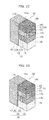
- FIG. 2A is a perspective view of a non-volatile memory cell array according to Embodiment 2 of the present invention.
- FIG. 2C is a cross-sectional diagram taken from the line B-B′ of the non-volatile memory cell array according to Embodiment 2 of the present invention.
- FIG. 3 is an equivalent circuit diagram of the non-volatile memory cell array according to Embodiment 2 of the present invention.
- FIG. 4 is a perspective view of the non-volatile memory cell array in a manufacturing step according to Embodiment 2 of the present invention.
- FIG. 5 is a perspective view of the non-volatile memory cell array in a manufacturing step according to Embodiment 2 of the present invention.
- FIG. 6 is a perspective view of the non-volatile memory cell array in a manufacturing step according to Embodiment 2 of the present invention.
- FIG. 7 is an exploded perspective view of a main section of the non-volatile memory cell array in a manufacturing step according to Embodiment 2 of the present invention.
- FIG. 8 is a graph which shows a progression rate of oxidation of a material used for the non-volatile memory cell array according to Embodiment 2 of the present invention.
- FIG. 9 is a perspective view of the non-volatile memory cell array in a manufacturing step according to Embodiment 2 of the as present invention.
- FIG. 10 is a perspective view of the non-volatile memory cell array in a manufacturing step according to Embodiment 2 of the present invention.
- FIG. 11 is a perspective view of the non-volatile memory cell array in a manufacturing step according to Embodiment 2 of the present invention.
- FIG. 12 is a perspective view of the non-volatile memory cell array in a manufacturing step according to Embodiment 2 of the present invention.
- FIG. 13 is a perspective view of the non-volatile memory cell array in a manufacturing step according to Embodiment 2 of the present invention.
- FIG. 14 is an exploded perspective view of a main section of the non-volatile memory cell array in a manufacturing step according to Embodiment 2 of the present invention.
- FIG. 15A is a perspective view of a non-volatile memory cell array according to a modification of Embodiment 2 of the present invention.
- FIG. 15B is a cross-sectional diagram taken from the line A-A′ of the non-volatile memory cell array according to the modification of Embodiment 2 of the present invention.
- FIG. 16 is a cross-sectional diagram of a non-volatile memory cell array, and an enlarged view and an equivalent circuit diagram of a memory cell according to a conventional example.
- FIG. 17 is a cross-sectional diagram of the non-volatile memory cell according to the conventional example.
- FIG. 1A to FIG. 1C show a non-volatile memory cell 10 according to Embodiment 1 of the present invention.
- FIG. 1A is a cross-sectional diagram of the non-volatile memory cell 10
- FIG. 1B is an equivalent circuit diagram of the non-volatile memory cell 10
- FIG. 1C is a perspective view of the non-volatile memory cell 10 .
- the non-volatile memory cell 10 includes: a columnar electrode 12 ; an interlayer insulating film 16 ; a variable resistance layer 14 ; a first conductive layer 13 ; and a semiconductor layer 17 ; and a second conductive layer 18 .
- the first conductive layer 13 As part of the first conductive layer 13 , the first variable resistance layer 13 a , the second variable resistance layer 13 b , and the insulating layer 13 c are formed.
- the variable resistance layer 14 includes the first variable resistance layer 13 a and the second variable resistance layer 13 b .
- insulating layers 17 a , 17 b , 18 a , and 18 b are formed.
- the interlayer insulating film 16 is formed in parallel to a main surface of a substrate (not illustrated).
- the first conductive layer 13 is disposed in contact with the interlayer insulating film 16 in a stacking direction.
- the semiconductor layer 17 is disposed in contact with the first conductive layer 13 in the stacking direction.
- the second conductive layer 18 is disposed in contact with the semiconductor layer 17 in the stacking direction.
- the first conductive layer 13 , the semiconductor layer 17 , and the second conductive layer 18 may be stacked in order indicated in FIG. 1A and FIG. 1C , or may be stacked in the inverse order.
- the columnar electrode 12 , the variable resistance layer 14 , and the first conductive layer 13 are included in the variable resistance element 15 in parallel with the main surface of the substrate.
- the first conductive layer 13 , the semiconductor layer 17 , and the second conductive layer 18 are included in a diode element 19 of an MSM (metal-semiconductor-metal) type having a bidirectional rectification property in a direction perpendicular to the main surface of the substrate.
- MSM metal-semiconductor-metal
- the non-volatile memory cell 10 is configured in which the variable resistance element 15 and the diode element 19 are connected to each other in series, as shown in the equivalent circuit diagram of FIG. 1B . It is to be noted that, in FIG. 1B , each of the columnar electrode 12 and the second conductive layer 18 is depicted as a line.
- the variable resistance layer 14 is interposed between the columnar electrode 12 and the first conductive layer 13 .
- the variable resistance layer 14 has a characteristic of changing between at least two states having different resistance values, and is capable of selectively causing a change from one state to another state.
- the non-volatile memory cell 10 is capable of selectively changing the resistance value between the columnar electrode 12 and the first conductive layer 13 , by applying a driving voltage or a driving current between the columnar electrode 12 and the first conductive layer 13 .
- the variable resistance layer 14 typically, has two states; that is, a high resistance state having a relatively high electric resistance value and a low resistance state having a low electric resistance value. At this time, the non-volatile memory cell 10 changes from the high resistance state to the low resistance state, or from the low resistance state to the high resistance state, according to an application of a driving voltage or a driving current equal to or larger than a predetermined threshold.
- the variable resistance layer 14 can be formed using a oxygen-deficient metal oxide.
- a constituent metal of the metal oxide is preferably a transition metal, such as tantalum (Ta), hafnium (Hf), titanium (Ti), tungsten (W), nickel (Ni), iron (Fe) and the like.
- an oxygen-deficient metal oxide refers to a metal oxide having a smaller amount of oxygen content than a composition of a metal oxide having a stoichiometric composition (insulator, in general), and many of them generally behave like semiconductors. It is possible to stably cause a resistance change between binary resistance values with an excellent reproducibility, by using an oxygen-deficient oxide of the above-exemplified constituent metal as the variable resistance layer 14 .
- the oxygen content of the variable resistance layer 14 decreases from an interface between the variable resistance layer 14 and the columnar electrode 12 , toward the first conductive layer 13 . It is possible to form the variable resistance layer 14 through an oxidation process such that the oxygen content of the variable resistance layer 14 continuously decreases with distance from the columnar electrode 12 . This is because that, in the oxidation process, the amount of oxygen entering an inside of the first conductive layer 13 decreases with distance from a contact hole. Among them, a layer having a higher oxygen content is the first variable resistance layer 13 a and the layer having a lower oxygen content is the second variable resistance layer 13 b.
- the first variable resistance layer 13 a receives an oxygen ion from the second variable resistance layer 13 b in response to an application of a positive driving voltage or a driving current (a current flows in the direction from the first variable resistance layer 13 a to the second variable resistance layer 13 b ) and changes to the high resistance state.
- the first variable resistance layer 13 a diffuses the received oxygen ion to the second variable resistance layer 13 b in response to an application of a negative driving voltage or a driving current and changes to the low resistance state.
- first variable resistance layer 13 a may change to the low resistance state only in part of the region of the first variable resistance layer 13 a .
- Patent Literature 4 Patent Literature 4
- variable resistance layer 14 is not limited to having two layers.
- a forming process may be performed on the variable resistance layer 14 .
- the forming process is a process of applying, once or plural times, a positive or negative voltage higher than a voltage applied during a normal operation, to the variable resistance layer 14 , in order to electrically form a layer having a large amount of oxygen content near the interface to which the positive voltage is applied.
- an oxygen-deficient metal oxide having less oxygen content (in resistivity, for example, equal to or less than 10 m ⁇ cm) or a metal which does not include oxygen may be used.
- the variable resistance layer 14 is easily formed from the first conductive layer 13 .
- resistance of the first conductive layer 13 decreases and thus power consumption can be reduced.
- the semiconductor layer 17 comprises SiN y , for example.
- Each of the first conductive layer 13 and the second conductive layer 18 is a material to form a Schottky junction by being in contact with the semiconductor layer 17 .
- the MSM diode includes the first conductive layer 13 , the semiconductor layer 17 , and the second conductive layer 18 .
- the second conductive layer 18 may comprise TiN, TaN, or the like.
- an MSM diode in which the first conductive layer 13 comprises TaO x , the semiconductor layer 17 comprises SiN y , and the second conductive layer 18 comprises TaN has a bidirectional rectification property for the applied voltage and provides a current steering element having a large breakdown current.
- the MSM diode can also easily create a non-volatile memory device and a non-volatile memory apparatus with high reliability, by combining a diode element and the variable resistance element.
- the variable resistance layer 14 is formed by (i) stacking the first conductive layer 13 , the semiconductor layer 17 , and the second conductive layer 18 in this order above the interlayer insulating film 16 , (ii) forming a contact hole that penetrates through a stacked body including the first conductive layer 13 , the semiconductor layer 17 , and the second conductive layer 18 , and the interlayer insulating film 16 in the stacking direction, and then (iii) performing oxidation process on part of the first conductive layer 13 exposed in the contact hole.
- the step of embedding a material into the contact hole includes only one step of embedding the columnar electrode 12 , and thus it is possible to simplify the manufacturing procedures.
- the variable resistance layer 14 by forming the variable resistance layer 14 through the oxidation process, there is an advantage that it is easy to control the thickness of the variable resistance layer 14 .
- part of the SiN y layer of the semiconductor layer 17 exposed to the contact hole is oxidized simultaneously with the oxidation of the first conductive layer 13 , an insulating layer 17 a comprising SiO 2 is formed on the surface, the semiconductor layer 17 is insulated from the columnar electrode 12 .
- part of the TaN, TiN, and the like of the second conductive layer 18 exposed to the contact hole is simultaneously oxidized, an insulating layer 18 a comprising TaON, TiON, and the like is formed, and the second conductive layer 18 is insulated from the columnar electrode 12 .
- the columnar electrode 12 may comprise a material which excels in conductivity (in resistivity, for example, equal to or less than 10 m ⁇ cm) and of which the major metal material has a standard electrode potential that is higher than a standard electrode potential of a metal included in the variable resistance layer 14 .
- Specific examples of the material of the columnar electrode 12 include: platinum (Pt), iridium (Ir), palladium (Pd), copper (Cu), tungsten (W) (excepting the case where the variable resistance layer is a tungsten oxide), and so on.
- the columnar electrode 12 may include a thin film formed of the above-exemplified material on an outer periphery of the conductive body comprising tungsten (W) or the like.
- the standard electrode potential of the metal used for the columnar electrode 12 is higher than the standard electrode potential of the metal used for the first conductive layer 13 and the variable resistance layer 14 is that, with this, since the columnar electrode 12 becomes difficult to be oxidized by the variable resistance layer 14 , oxidation-reduction reaction of the variable resistance layer 14 mainly occurs near the interface between the columnar electrode 12 and the variable resistance layer 14 , the oxygen content of the first variable resistance layer 13 a changes, thereby stabilizing resistance changing phenomenon.
- the variable resistance layer 14 is formed in one oxidation process and, at the same time, an insulating film for electrically isolating each of the semiconductor layer 17 and the second conductive layer 18 from the columnar electrode 12 , and thus it is possible to simplify the is manufacturing procedures.
- the uniformity of the thickness of the variable resistance layer can easily be controlled, so that the reliability of the non-volatile memory cell array increases.
- FIG. 1D is a diagram showing an example of a structure of a non-volatile memory cell 30 according to a modification of Embodiment 1 of the present invention.
- variable resistance element 15 included in the non-volatile memory cell 10 of FIG. 1C is replaced with a variable resistance element 35 including a variable resistance layer 34 comprising a first variable resistance layer 31 and a second variable resistance layer 32 .
- the columnar electrode 12 , the variable resistance layer 34 , and the first conductive layer 13 are included in the variable resistance element 35 in parallel with the main surface of the substrate.
- the first conductive layer 13 , the semiconductor layer 17 , and the second conductive layer 18 are included in a diode element 19 of an MSM type having a bidirectional rectification property in a direction perpendicular to the main surface of the substrate.
- the non-volatile memory cell 30 shares characteristics with the non-volatile memory cell 10 in that the variable resistance layer 34 is provided between the columnar electrode 12 and the first conductive layer 13 , the variable resistance element 35 is disposed in parallel with the main surface of the substrate, and the diode element 19 is disposed perpendicular to the main surface of the substrate. With these common characteristics, the non-volatile memory cell 30 and the non-volatile memory cell 10 have the advantages described below.
- Each of the variable resistance elements 15 and 35 has a resistance value that changes due to a change in a filament (conductive path) in each of the variable resistance layers 14 and 34 .
- the higher voltage or the denser current is applied to the variable resistance layers 14 and 34 , the more likely the resistance value changes. It is preferable, therefore, that an area of each of the variable resistance elements 15 and 35 is small.
- the area refers to an area of a surface perpendicular to the direction of applying a voltage.
- the diode element 19 causes a large current (for example, at least 10000 A/cm 2 ) to flow through the variable resistance elements 15 and 35 , it is preferable that the current capacity is large.
- the current capacity of the diode increases depending on the size of the junction area of the diode, and thus it is preferable that the area of the diode element 19 is large.
- the non-volatile memory cells 10 and 30 since the direction of applying a voltage to the variable resistance elements 15 and 35 is different from the direction of applying a voltage to the diode element 19 , it is possible to reduce the area of the variable resistance elements 15 and 35 on one hand and to increase the area of the diode element 19 on the other hand.
- the area of each of the variable resistance elements 15 and 35 is defined by the thickness of the first conductive layer 13 stacked horizontally with respect to the main surface of the substrate, it is possible to make the area of each of the variable resistance elements 15 and 35 equal to or less than a minimum fabrication size, for example.
- the non-volatile memory cell 30 is different from the non-volatile memory cell 10 in that the first variable resistance layer 31 is formed to be in contact with a side face of the columnar electrode 12 and to cover the side face, and the second variable resistance layer 32 is formed exclusively at an intersection of the first variable resistance layer 31 and the first conductive layer 13 .
- the non-volatile memory cell 30 can be manufactured, in the same manner as the manufacturing steps of the non-volatile memory cell 10 , by forming a contact hole for embedding the columnar electrode 12 and then embedding the first variable resistance layer 31 and the columnar electrode 12 in this order in the contact hole.
- the step of embedding a material into a contact hole is composed of two steps; that is, embedding of the first variable resistance layer 31 and embedding of the columnar electrode 12 , and thus it is possible to separate the step of forming the first variable resistance layer 31 from the step of forming the second variable resistance layer 32 .
- the non-volatile memory cell 30 although there is a slight decrease in the simplification of the manufacturing procedures and the controllability of the thickness of the variable resistance layer 34 compared to the non-volatile memory cell 10 , it is possible to obtain an advantage that flexibility in selecting a material for the first variable resistance layer 31 and the second variable resistance layer 32 increases.
- the first variable resistance layer 31 and the second variable resistance layer depending on a desired variable resistance characteristic, an oxidation characteristic, and so on. It is possible to use, for example, at least one material having a high resistivity selected from a titanium oxide (TiO 2 , for example), a hafnium oxide (HfO y ), an aluminum oxide (AlO y ), and the like, for the first variable resistance layer 31 , and to use a tantalum oxide (TaO x ) having a lower resistance value than a resistance value of the first variable resistance layer 31 for the second variable resistance layer 32 .
- TiO 2 titanium oxide
- HfO y hafnium oxide
- AlO y aluminum oxide
- transition metal oxides of different types can be used for the first variable resistance layer 31 and the second variable resistance layer 32 , for example.
- a transition metal oxide having a lower degree of oxygen deficiency than a degree of oxygen deficiency of a transition metal oxide of the second variable resistance layer 32 is used for the first variable resistance layer 31 .
- the degree of oxygen deficiency is a ratio of deficient oxygen to the amount of oxygen included in the stoichiometric oxide in each of the transition metals.
- the composition of the stoichiometric oxide is Ta 2 O 5 , and thus it can be denoted as TaO 2.5 .
- the degree of oxygen deficiency of TaO 2.5 is 0%.
- the oxygen content atomic percentage of Ta 2 O 5 is the ratio of oxygen to a total number of atoms (O/(Ta+0)); that is 71.4 atm %. Accordingly, the oxygen content atomic percentage of the oxygen-deficient tantalum oxide is larger than 0 and smaller than 71.4 atm %.
- the degree of oxygen deficiency is smaller as the oxygen content atomic percentage (oxygen content) is larger, and the degree of oxygen deficiency is larger as the oxygen content atomic percentage (oxygen content) is smaller.
- the degree of oxygen deficiency is used instead of the above-described oxygen content, as a measure for uniformly comparing the deficient degrees of oxidation of the transition metal oxides irrespective of the types of the constituent metals.
- a transition metal oxide having a degree of oxygen deficiency smaller than a degree of oxygen deficiency of a transition metal oxide of the second variable resistance layer 32 is used for the first variable resistance layer 31 , so that a larger amount of voltages, among voltages applied between the first conductive layer 13 and the columnar electrode 12 during the resistance change, are distributed to the first variable resistance layer 31 of the variable resistance layer 34 , thereby facilitating oxidation-reduction reaction occurring in the first variable resistance layer 31 of the variable resistance layer 34 .
- the standard electrode potential of the transition metal of the first variable resistance layer 31 is lower than the standard electrode potential of the transition metal of the second variable resistance layer 32 .
- the resistance changing phenomenon is considered to occur as a result of a change in a resistance value caused by the oxidation-reduction reaction in a minute filament (conductive path) formed in the transition metal oxide layer of the first variable resistance layer 31 having a high resistance.
- the oxidation-reduction reaction is facilitated in the transition metal oxide of the first variable resistance layer 31 , by providing, as the transition metal oxide of the first variable resistance layer 31 , a transition metal oxide having a lower standard electrode potential than a standard electrode potential of a transition metal oxide of the second variable resistance layer 32 .
- the columnar electrode 12 of the non-volatile memory cell 30 comprises a material of which a standard electrode potential of a major metal material is higher than a standard electrode potential of a metal comprised by the first variable resistance layer 31 .
- This is based on the same concept as the non-volatile memory cell 10 . More specifically, since the columnar electrode 12 formed as described above is more difficult to oxidize than the first variable resistance layer 31 , oxidation-reduction reaction of the first variable resistance layer 31 mainly occurs near the interface of the columnar electrode 12 and the first variable resistance layer 31 , and the oxygen content of the first variable resistance layer 31 changes, thereby stabilizing the resistance changing phenomenon.
- FIG. 2A to FIG. 2C , and FIG. 3 show an example of a non-volatile memory cell array 20 according to Embodiment 2 of the present invention.
- FIG. 2A is a perspective view of the non-volatile memory cell array 20 .
- FIG. 2B and FIG. 2C are cross-sectional diagrams of the non-volatile memory cell 20 taken from the line A-A′ and the line B-B′, respectively, in the perspective view of the non-volatile memory cell array 20 .
- FIG. 3 is an equivalent circuit diagram of the non-volatile memory cell array 20 .
- an explanation will be given in line with the directions of X, Y, and Z shown by arrows in the diagram.
- the non-volatile memory cell array 20 is a memory cell array in which three interlayer insulating films 16 and three stacked bodies 21 are alternately arranged in the Z direction (direction perpendicular to the substrate), each of the stacked bodies 21 includes 20 memory cells (four in the X direction ⁇ five in the Y direction), and a total of 60 memory cells are three-dimensionally arranged.
- the non-volatile memory cell array 20 is formed above a substrate (not illustrated) including a main surface that is parallel to in the XY face.
- each of the memory cells corresponds to the non-volatile memory cell 10 according to Embodiment 1, and includes: a columnar electrode 12 ; an interlayer insulating film 16 ; a first conductive layer 13 ; a variable resistance layer 14 having a first variable resistance layer 13 a and a second variable resistance layer 13 b ; a semiconductor layer 17 ; and a second conductive layer 18 .
- the non-volatile memory cell 10 is represented in the cross-sectional diagram of FIG. 2B .
- the columnar electrode 12 is not included and the first conductive layer 13 is oxidized over the entire width in the X direction to be an insulating layer 13 c .
- the cross-sectional structure shown in FIG. 2C serves as element isolation for isolating the non-volatile memory cells 10 adjacent to each other in the Y direction.
- the non-volatile memory cell array 20 in the same manner as Embodiment 1, since the variable resistance layer 14 is formed by performing an oxidation process on part of the first conductive layer 13 after forming a contact hole, it is possible to simplify the manufacturing procedures. In addition, since the variable resistance layer 14 is formed exclusively at an intersection of the columnar electrode 12 and the first conductive layer 13 , it is possible to implement a memory cell array in which the variable resistance layer 14 is isolated for each memory cell. Furthermore, compared to the variable resistance layer formed by embedding, the thickness of the variable resistance layer 14 formed by the oxidation process can be controlled uniformly over a plurality of variable resistance layers 14 in the contact hole. Thus, the reliability of the non-volatile memory cell array 20 of the stacking structure improves.
- each of the columnar electrodes 12 has a columnar shape perpendicular to the main surface of the substrate, disposed at positions distributed in matrix on the main surface of the substrate (in other words, distributed in array in the X direction and in the Y direction), and serves as a bit line.
- each of the second conductive layers 18 serves as a word line.
- the insulating layer 26 which has a planer shape and is disposed at a Y-Z plane in the center portion in FIG. 2A divides, at the center of the non-volatile memory cell array 20 , the memory cells 10 arranged in each row four by four in the row (X) direction, into two groups each including two of the memory cells 10 . More specifically, in FIG. 2A , the columnar electrodes 12 of the memory cell 10 positioned at both sides of the insulating layer 26 provided at the Y-Z plane in the center is isolated from each other by the insulating layer 26 .
- such a structure is repeatedly provided in the X direction, thereby allowing reduction of a sneak current that passes through an unselected bit line, an unselected word line, and an unselected memory cell.
- FIG. 3 is an equivalent circuit diagram of the non-volatile memory cell array 20 according to Embodiment 2.
- the non-volatile memory cell 10 is provided at a crosspoint of the columnar electrode 12 (bit line: B 00 , B 01 , . . . , B 11 , . . . ) and the second conductive layer 18 (word line: W 00 , W 01 , . . . , W 30 , W 31 , . . . ).
- the state of a resistance value of the non-volatile memory cell 10 can be changed by selecting a bit line (B 00 , for example) and a word line (W 00 , for example) and applying a driving voltage to the non-volatile memory cell 10 positioned at a crosspoint thereof. Accordingly, when assigning information in association with the state of the resistance value of the non-volatile memory cell 10 , it is possible to write information to or read information from the non-volatile memory cell 10 by applying a driving voltage to the bit line and the word line each of which is connected to the non-volatile memory cell 10 . As a result, it is possible to implement the non-volatile memory cell array 20 that has random access capability.
- the memory cell array including the bit lines B 00 to B 04 and the word lines W 00 to W 12 are completely separated in a line level from the memory cell array including the bit lines B 10 to B 14 and the word lines W 20 to W 32 , and thus it is possible to reduce a sneak current.
- the following describes a manufacturing method of the non-volatile memory cell array according to Embodiment 2 with reference to FIG. 4 to FIG. 14 .
- the interlayer insulating films 16 and the stacked bodies 21 are alternately stacked above a substrate (not illustrated) in parallel with the main surface of the substrate.
- Each of the stacked bodies 21 includes the first conductive layer 13 , the semiconductor layer 17 , and the second conductive layer 18 .
- the stacked body 21 includes three layers. However, the number of layers included in the stacked body 21 is not particularly limited to this.
- tantalum (Ta) or an oxygen-deficient tantalum oxide TaO x is deposited as the first conductive layer 13 through sputtering, for example, and silicon nitride SiN y is deposited as the semiconductor layer 17 through sputtering.
- tantalum nitride (TaN) is deposited as the second conductive layer 18 through sputtering. In each sputtering, reactive sputtering which introduces oxygen or nitrogen during sputtering may be used.
- interlayer insulating film 16 may be formed further above the second conductive layer 18 in the topmost layer.
- a strip-shaped trench 27 is formed along the Y-Z direction perpendicular to the main surface of the stacking structure.
- a plasma oxidation process is performed in an oxygen atmosphere with 1100 W of an application power for 30 seconds of processing time, for example.
- Active oxygen, oxygen ions, or oxygen atoms diffuse from the surface of the first conductive layer 13 exposed to the strip-shaped trench 27 toward an inside of the first conductive layer 13 .
- Due to these oxygen species an oxide is formed which has a profile of a predetermined degree of oxygen deficiency in a region having a certain thickness from the surface exposed to the strip-shaped trench 27 toward the inside of the first conductive layer 13 .
- the profile of the degree of oxygen deficiency is high near the surface and continuously decreases toward the inside.
- variable resistance layer 14 is formed to have a thickness of approximately 10 nm from the surface exposed to the strip-shaped trench 27 .
- first variable resistance layer 13 a having a lower degree of oxygen deficiency is formed in a region including approximately 2 to 3 nm from the surface
- second variable resistance layer 13 b having a higher degree of oxygen deficiency is formed in a region including approximately 7 to 8 nm from the first variable resistance layer 13 a.
- the plasma oxidation process is performed in an oxygen atmosphere according to the processes to form the variable resistance layer 14 as described above; however, the present invention is not limited to this.
- heating treatment hereinafter referred to as a thermal oxidation process
- the thermal oxidation process and the plasma oxidation process as described above are collectively called an oxidation process in the description below.
- the variable resistance layer 14 is formed by performing oxidation process on part of the first conductive layer 13 , it is possible to simplify the conventional manufacturing procedures including the steps of embedding conductive layers.
- thickness control is easily conducted through the oxidation process compared to the embedding process, and thus the variable resistance layers 14 exposed to the strip-shaped trench 27 are formed to be uniform in thickness.
- approximately 10 nm of TaO x that is the first conductive layer 13 is oxidized from the surface.
- An oxidized portion of the first conductive layer 13 serves as the first variable resistance layer 13 a and the second variable resistance layer 13 b.
- SiN y that is the semiconductor layer 17 is oxidized from the surface to be SiO 2 that includes nitrogen and is an insulator.
- An oxidized portion of the semiconductor layer 17 serves as the insulating layers 17 a and 17 b.
- each of the first conductive layer 13 , the semiconductor layer 17 , and the second conductive layer 18 is oxidized in a portion that is different in size from each other, due to the difference in the respective materials.
- the difference in the progression rate of oxidation between the first conductive layer 13 and the second conductive layer 18 has an important meaning also in the oxidation process for providing element isolation described below.
- a polysilicon 28 is deposited by CVD in the strip-shaped trench 27 previously formed. Then, through CMP process and other planarization processes, unnecessary polysilicons are polished and removed to leave the polysilicon 28 formed in the strip-shaped trench 27 .
- a photoresist mask pattern having a predetermined pattern shape is formed through a general photolithography process.
- the stacking structure is etched using the photoresist mask pattern to form the contact hole 29 .
- the mask pattern is removed.
- a hard mask may be used.
- the columnar electrode 12 is deposited in the contact hole 29 by sputtering, CVD, plating, or the like.
- a conductive material such as platinum (Pt), iridium (Ir), palladium (Pd), copper (Cu), and tungsten (W), are used, for example.
- CMP chemical mechanical polishing
- unnecessary electrode materials are polished and removed to leave the columnar electrode 12 formed inside the contact hole 29 .
- the columnar electrode 12 is directly in contact with the first variable resistance layer 13 a , connected to the semiconductor layer 17 via the insulating layer 17 , and connected to the second conductive layer 18 via the insulating layer 18 a.
- the polysilicon 28 disposed in a region other than the columnar electrode 12 in the strip-shaped trench 27 is removed by wet etching using HF:HNO 3 solution.
- oxidation process is performed on the interlayer insulating film 16 , the first conductive layer 13 , the semiconductor layer 17 , and the second conductive layer 18 which are exposed to a space (for simplification, this space is also called the strip-shaped trench 27 ), created by removing the polysilicon 28 in the strip-shaped trench 27 .
- the thickness of TaON increases in the region of the second conductive layer 18 exposed to the strip-shaped trench 27 , but a region of TaN that is the second conductive layer 18 remains inside because the oxidation rate of the TaON is lower than TaO that is the first conductive layer 13 as shown in the graph of FIG. 8 , and thus the remaining region of TaN can serve as a word line.
- the filling material is a material that can be temporarily embedded in the strip-shaped trench and, in a subsequent step, selectively removed by wet etching or the like while leaving the interlayer insulating film 16 and the stacked bodies 21 including the first conductive layer 13 , the semiconductor layer 17 , and the second conductive layer 18 .
- FIG. 15A is a perspective view of an example of a non-volatile memory cell array 40 according to a modification of Embodiment 2 of the present invention.
- FIG. 15B is a cross-sectional diagram taken from the line A-A′ in the perspective view of the non-volatile memory cell array 40 shown in FIG. 15A . It is to be noted that the cross-sectional diagram taken from the line B-B′ of the non-volatile memory cell array 40 is the same as the cross-sectional diagram taken from the line B-B′ of the non-volatile memory cell array 20 shown in FIG. 2C , and thus the illustration is omitted.
- the non-volatile memory cell 10 included in the non-volatile memory cell array 20 shown in FIG. 2A and FIG. 2B is replaced with the non-volatile memory cell 30 according to the modification of Embodiment 1.
- the non-volatile memory cell array 40 is different from the non-volatile memory cell array 20 in that the first variable resistance layer 31 is in contact with the side face of the columnar electrode 12 and formed to cover the side face. As shown in FIG. 15A and FIG. 15B , the non-volatile memory cell array 40 includes the first variable resistance layer 31 that is continuously provided not only at an intersection of the columnar electrode 12 and the second variable resistance layer 32 but also at an intersection of the columnar electrode 12 and the semiconductor layer 17 , at an intersection of the columnar electrode 12 and the second conductive layer 18 , and at an intersection of the columnar electrode 12 and the interlayer insulating film 16 .
- such a shape is obtained by embedding the first variable resistance layer 31 and the columnar electrode 12 in this order in the contact hole.
- a material of the first variable resistance layer 31 is deposited on an inner wall of the contact hole 29 to be shaped into a thin film, by sputtering, CVD, plating, or the like, before forming the columnar electrode 12 in the step shown in FIG. 11 .
- a material of the first variable resistance layer 31 for example, a transition metal oxide of which a constituent metal is tantalum (Ta), hafnium (Hf), titanium (Ti), tungsten (W), nickel (Ni), iron (Fe), or the like can be used, and in particular, a transition metal oxide of which a constituent metal is different from a constituent metal of the second variable resistance layer 32 can be used.
- the step of embedding a material into a contact hole is composed of two steps; that is, embedding of the first variable resistance layer 31 and embedding of the columnar electrode 12 , and thus it is possible to separate the step of forming the first variable resistance layer 31 from the step of forming the second variable resistance layer 32 .
- the non-volatile memory cell array 40 although there is a slight decrease in the simplification of the manufacturing procedures and the controllability of the thickness of the variable resistance layer 34 compared to the non-volatile memory cell array 20 , it is possible to obtain an advantage that flexibility in selecting a material for the first variable resistance layer 31 increases.
- the manufacturing method according to the present invention is applicable, without being limited to the non-volatile memory cell array that is exemplified in the present embodiment 2. More specifically, it is possible to manufacture any electronic devices in which a variable resistance element is included, by applying the above-described manufacturing method or combining the above-described manufacturing method and a known method.
- the non-volatile memory cell array according to the present invention is useful as a next-generation non-volatile memory and the like which is directed to lower power consumption, higher-speed writing, higher-speed deleting, and larger capacity.
Landscapes
- Engineering & Computer Science (AREA)
- Manufacturing & Machinery (AREA)
- Semiconductor Memories (AREA)
Applications Claiming Priority (3)
| Application Number | Priority Date | Filing Date | Title |
|---|---|---|---|
| JP2010-151400 | 2010-07-01 | ||
| JP2010151400 | 2010-07-01 | ||
| PCT/JP2011/003697 WO2012001960A1 (ja) | 2010-07-01 | 2011-06-29 | 不揮発性メモリセル、不揮発性メモリセルアレイ、およびその製造方法 |
Publications (2)
| Publication Number | Publication Date |
|---|---|
| US20120104351A1 US20120104351A1 (en) | 2012-05-03 |
| US9006793B2 true US9006793B2 (en) | 2015-04-14 |
Family
ID=45401700
Family Applications (1)
| Application Number | Title | Priority Date | Filing Date |
|---|---|---|---|
| US13/382,321 Active 2032-10-10 US9006793B2 (en) | 2010-07-01 | 2011-06-29 | Non-volatile memory cell, non-volatile memory cell array, and method of manufacturing the same |
Country Status (4)
| Country | Link |
|---|---|
| US (1) | US9006793B2 (zh) |
| JP (1) | JP4921620B2 (zh) |
| CN (1) | CN102473707A (zh) |
| WO (1) | WO2012001960A1 (zh) |
Cited By (4)
| Publication number | Priority date | Publication date | Assignee | Title |
|---|---|---|---|---|
| US20150255715A1 (en) * | 2014-03-07 | 2015-09-10 | Kabushiki Kaisha Toshiba | Nonvolatile memory device |
| US9704922B2 (en) | 2015-05-29 | 2017-07-11 | Kabushiki Kaisha Toshiba | Semiconductor memory device and method of manufacturing the same while avoiding process damage to a variable resistance film |
| US9721961B2 (en) | 2015-05-29 | 2017-08-01 | Kabushiki Kaisha Toshiba | Semiconductor memory device |
| US10804325B2 (en) | 2018-03-23 | 2020-10-13 | Toshiba Memory Corporation | Semiconductor memory device |
Families Citing this family (70)
| Publication number | Priority date | Publication date | Assignee | Title |
|---|---|---|---|---|
| US9570678B1 (en) | 2010-06-08 | 2017-02-14 | Crossbar, Inc. | Resistive RAM with preferental filament formation region and methods |
| US9012307B2 (en) | 2010-07-13 | 2015-04-21 | Crossbar, Inc. | Two terminal resistive switching device structure and method of fabricating |
| US8946046B1 (en) | 2012-05-02 | 2015-02-03 | Crossbar, Inc. | Guided path for forming a conductive filament in RRAM |
| US9601692B1 (en) | 2010-07-13 | 2017-03-21 | Crossbar, Inc. | Hetero-switching layer in a RRAM device and method |
| WO2011156787A2 (en) | 2010-06-11 | 2011-12-15 | Crossbar, Inc. | Pillar structure for memory device and method |
| US8441835B2 (en) | 2010-06-11 | 2013-05-14 | Crossbar, Inc. | Interface control for improved switching in RRAM |
| US8374018B2 (en) | 2010-07-09 | 2013-02-12 | Crossbar, Inc. | Resistive memory using SiGe material |
| US8884261B2 (en) | 2010-08-23 | 2014-11-11 | Crossbar, Inc. | Device switching using layered device structure |
| US8168506B2 (en) | 2010-07-13 | 2012-05-01 | Crossbar, Inc. | On/off ratio for non-volatile memory device and method |
| US8467227B1 (en) | 2010-11-04 | 2013-06-18 | Crossbar, Inc. | Hetero resistive switching material layer in RRAM device and method |
| US8947908B2 (en) | 2010-11-04 | 2015-02-03 | Crossbar, Inc. | Hetero-switching layer in a RRAM device and method |
| US8569172B1 (en) | 2012-08-14 | 2013-10-29 | Crossbar, Inc. | Noble metal/non-noble metal electrode for RRAM applications |
| US8889521B1 (en) | 2012-09-14 | 2014-11-18 | Crossbar, Inc. | Method for silver deposition for a non-volatile memory device |
| US8492195B2 (en) | 2010-08-23 | 2013-07-23 | Crossbar, Inc. | Method for forming stackable non-volatile resistive switching memory devices |
| US9401475B1 (en) | 2010-08-23 | 2016-07-26 | Crossbar, Inc. | Method for silver deposition for a non-volatile memory device |
| US8404553B2 (en) * | 2010-08-23 | 2013-03-26 | Crossbar, Inc. | Disturb-resistant non-volatile memory device and method |
| US8391049B2 (en) | 2010-09-29 | 2013-03-05 | Crossbar, Inc. | Resistor structure for a non-volatile memory device and method |
| US8558212B2 (en) | 2010-09-29 | 2013-10-15 | Crossbar, Inc. | Conductive path in switching material in a resistive random access memory device and control |
| US8502185B2 (en) | 2011-05-31 | 2013-08-06 | Crossbar, Inc. | Switching device having a non-linear element |
| USRE46335E1 (en) | 2010-11-04 | 2017-03-07 | Crossbar, Inc. | Switching device having a non-linear element |
| US8088688B1 (en) | 2010-11-05 | 2012-01-03 | Crossbar, Inc. | p+ polysilicon material on aluminum for non-volatile memory device and method |
| US8930174B2 (en) | 2010-12-28 | 2015-01-06 | Crossbar, Inc. | Modeling technique for resistive random access memory (RRAM) cells |
| US8791010B1 (en) | 2010-12-31 | 2014-07-29 | Crossbar, Inc. | Silver interconnects for stacked non-volatile memory device and method |
| US8815696B1 (en) | 2010-12-31 | 2014-08-26 | Crossbar, Inc. | Disturb-resistant non-volatile memory device using via-fill and etchback technique |
| US9153623B1 (en) | 2010-12-31 | 2015-10-06 | Crossbar, Inc. | Thin film transistor steering element for a non-volatile memory device |
| US8450710B2 (en) | 2011-05-27 | 2013-05-28 | Crossbar, Inc. | Low temperature p+ silicon junction material for a non-volatile memory device |
| US8394670B2 (en) | 2011-05-31 | 2013-03-12 | Crossbar, Inc. | Vertical diodes for non-volatile memory device |
| US9620206B2 (en) | 2011-05-31 | 2017-04-11 | Crossbar, Inc. | Memory array architecture with two-terminal memory cells |
| US8619459B1 (en) | 2011-06-23 | 2013-12-31 | Crossbar, Inc. | High operating speed resistive random access memory |
| US9564587B1 (en) | 2011-06-30 | 2017-02-07 | Crossbar, Inc. | Three-dimensional two-terminal memory with enhanced electric field and segmented interconnects |
| US8946669B1 (en) | 2012-04-05 | 2015-02-03 | Crossbar, Inc. | Resistive memory device and fabrication methods |
| US9166163B2 (en) | 2011-06-30 | 2015-10-20 | Crossbar, Inc. | Sub-oxide interface layer for two-terminal memory |
| US9627443B2 (en) | 2011-06-30 | 2017-04-18 | Crossbar, Inc. | Three-dimensional oblique two-terminal memory with enhanced electric field |
| US8659929B2 (en) | 2011-06-30 | 2014-02-25 | Crossbar, Inc. | Amorphous silicon RRAM with non-linear device and operation |
| US9252191B2 (en) | 2011-07-22 | 2016-02-02 | Crossbar, Inc. | Seed layer for a p+ silicon germanium material for a non-volatile memory device and method |
| US8674724B2 (en) | 2011-07-29 | 2014-03-18 | Crossbar, Inc. | Field programmable gate array utilizing two-terminal non-volatile memory |
| US10056907B1 (en) | 2011-07-29 | 2018-08-21 | Crossbar, Inc. | Field programmable gate array utilizing two-terminal non-volatile memory |
| US9729155B2 (en) | 2011-07-29 | 2017-08-08 | Crossbar, Inc. | Field programmable gate array utilizing two-terminal non-volatile memory |
| US8716098B1 (en) | 2012-03-09 | 2014-05-06 | Crossbar, Inc. | Selective removal method and structure of silver in resistive switching device for a non-volatile memory device |
| US9087576B1 (en) | 2012-03-29 | 2015-07-21 | Crossbar, Inc. | Low temperature fabrication method for a three-dimensional memory device and structure |
| US9685608B2 (en) | 2012-04-13 | 2017-06-20 | Crossbar, Inc. | Reduced diffusion in metal electrode for two-terminal memory |
| US8658476B1 (en) | 2012-04-20 | 2014-02-25 | Crossbar, Inc. | Low temperature P+ polycrystalline silicon material for non-volatile memory device |
| US8796658B1 (en) | 2012-05-07 | 2014-08-05 | Crossbar, Inc. | Filamentary based non-volatile resistive memory device and method |
| US8765566B2 (en) | 2012-05-10 | 2014-07-01 | Crossbar, Inc. | Line and space architecture for a non-volatile memory device |
| US9583701B1 (en) | 2012-08-14 | 2017-02-28 | Crossbar, Inc. | Methods for fabricating resistive memory device switching material using ion implantation |
| US10096653B2 (en) | 2012-08-14 | 2018-10-09 | Crossbar, Inc. | Monolithically integrated resistive memory using integrated-circuit foundry compatible processes |
| US8946673B1 (en) | 2012-08-24 | 2015-02-03 | Crossbar, Inc. | Resistive switching device structure with improved data retention for non-volatile memory device and method |
| JP2014049745A (ja) * | 2012-08-31 | 2014-03-17 | Toshiba Corp | 半導体記憶装置、及びその製造方法 |
| US20140077149A1 (en) * | 2012-09-14 | 2014-03-20 | Industrial Technology Research Institute | Resistance memory cell, resistance memory array and method of forming the same |
| US9312483B2 (en) | 2012-09-24 | 2016-04-12 | Crossbar, Inc. | Electrode structure for a non-volatile memory device and method |
| US9576616B2 (en) | 2012-10-10 | 2017-02-21 | Crossbar, Inc. | Non-volatile memory with overwrite capability and low write amplification |
| US11068620B2 (en) | 2012-11-09 | 2021-07-20 | Crossbar, Inc. | Secure circuit integrated with memory layer |
| US8982647B2 (en) | 2012-11-14 | 2015-03-17 | Crossbar, Inc. | Resistive random access memory equalization and sensing |
| US9412790B1 (en) | 2012-12-04 | 2016-08-09 | Crossbar, Inc. | Scalable RRAM device architecture for a non-volatile memory device and method |
| US10186658B2 (en) | 2012-12-26 | 2019-01-22 | Sony Semiconductor Solutions Corporation | Memory device and method of manufacturing memory device |
| US9406379B2 (en) | 2013-01-03 | 2016-08-02 | Crossbar, Inc. | Resistive random access memory with non-linear current-voltage relationship |
| US9112145B1 (en) | 2013-01-31 | 2015-08-18 | Crossbar, Inc. | Rectified switching of two-terminal memory via real time filament formation |
| US9324942B1 (en) | 2013-01-31 | 2016-04-26 | Crossbar, Inc. | Resistive memory cell with solid state diode |
| US8934280B1 (en) | 2013-02-06 | 2015-01-13 | Crossbar, Inc. | Capacitive discharge programming for two-terminal memory cells |
| US9214228B1 (en) * | 2013-08-22 | 2015-12-15 | Kabushiki Kaisha Toshiba | Semiconductor memory device and method of forming thereof |
| EP2887396B1 (en) | 2013-12-20 | 2017-03-08 | Imec | Three-dimensional resistive memory array |
| US9437296B2 (en) | 2014-02-03 | 2016-09-06 | Kabushiki Kaisha Toshiba | Three-dimensional resistive memory device with adjustable voltage biasing |
| US10290801B2 (en) | 2014-02-07 | 2019-05-14 | Crossbar, Inc. | Scalable silicon based resistive memory device |
| US9831290B2 (en) * | 2016-03-10 | 2017-11-28 | Toshiba Memory Corporation | Semiconductor memory device having local bit line with insulation layer formed therein |
| US11018189B2 (en) | 2017-04-11 | 2021-05-25 | Sony Semiconductor Solutions Corporation | Storage apparatus |
| US10825867B2 (en) | 2018-04-24 | 2020-11-03 | Micron Technology, Inc. | Cross-point memory array and related fabrication techniques |
| US10729012B2 (en) * | 2018-04-24 | 2020-07-28 | Micron Technology, Inc. | Buried lines and related fabrication techniques |
| JP7249062B2 (ja) * | 2019-07-24 | 2023-03-30 | 国立研究開発法人産業技術総合研究所 | 積層部を備える柱状構造体を有する電極 |
| US11362139B2 (en) * | 2019-12-26 | 2022-06-14 | SK Hynix Inc. | Electronic device and method of manufacturing the same |
| CN112054033A (zh) * | 2020-09-15 | 2020-12-08 | 中国科学院微电子研究所 | 一种存储器件 |
Citations (17)
| Publication number | Priority date | Publication date | Assignee | Title |
|---|---|---|---|---|
| US6753561B1 (en) * | 2002-08-02 | 2004-06-22 | Unity Semiconductor Corporation | Cross point memory array using multiple thin films |
| US20060081962A1 (en) | 2004-10-19 | 2006-04-20 | Matsushita Electric Industial Co., Ltd. | Variable resistance device made of a material which has an electric resistance value changing in accordance with an applied electric field and maintains the electric resistance value after being changed in a nonvolatile manner, and a semiconductor apparatus including the same |
| US20070015328A1 (en) * | 2005-07-18 | 2007-01-18 | Sharp Laboratories Of America, Inc. | MSM binary switch memory device |
| US20080175032A1 (en) | 2007-01-23 | 2008-07-24 | Kabushiki Kaisha Toshiba | Semiconductor memory and method for manufacturing the same |
| WO2008149484A1 (ja) | 2007-06-05 | 2008-12-11 | Panasonic Corporation | 不揮発性記憶素子およびその製造方法、並びにその不揮発性記憶素子を用いた不揮発性半導体装置 |
| JP2009081251A (ja) | 2007-09-26 | 2009-04-16 | Panasonic Corp | 抵抗変化素子とその製造方法ならびに抵抗変化型メモリ |
| US20090141547A1 (en) * | 2007-11-29 | 2009-06-04 | Samsung Electronics Co., Ltd. | Non-volatile memory devices and methods of fabricating and using the same |
| US20090146190A1 (en) * | 2007-11-30 | 2009-06-11 | Kabushiki Kaisha Toshiba | Semiconductor memory device and method for fabricating semiconductor memory device |
| US20090321878A1 (en) * | 2008-06-26 | 2009-12-31 | Koo June-Mo | Non-volatile memory device and method of fabricating the same |
| US20100072452A1 (en) * | 2008-09-19 | 2010-03-25 | Samsung Electronics Co., Ltd. | Non-volatile memory device |
| US20100157658A1 (en) * | 2008-12-19 | 2010-06-24 | Unity Semiconductor Corporation | Conductive metal oxide structures in non-volatile re-writable memory devices |
| US20100219392A1 (en) * | 2009-02-27 | 2010-09-02 | Nobuyoshi Awaya | Nonvolatile semiconductor memory device and manufacturing method for same |
| US20100321982A1 (en) * | 2008-12-18 | 2010-12-23 | Takeshi Takagi | Nonvolatile storage device and method for writing into the same |
| US20120104350A1 (en) * | 2010-04-28 | 2012-05-03 | Atsushi Himeno | Variable resistance nonvolatile memory device and method of manufacturing the same |
| US20130113080A1 (en) * | 2011-11-08 | 2013-05-09 | Takeshi HIOKA | Non-volatile semiconductor storage device |
| US8565003B2 (en) * | 2011-06-28 | 2013-10-22 | Unity Semiconductor Corporation | Multilayer cross-point memory array having reduced disturb susceptibility |
| US8859327B2 (en) * | 2010-02-26 | 2014-10-14 | Kabushiki Kaisha Toshiba | Method for manufacturing a non-volatile semiconductor memory device |
-
2011
- 2011-06-29 US US13/382,321 patent/US9006793B2/en active Active
- 2011-06-29 JP JP2011544316A patent/JP4921620B2/ja active Active
- 2011-06-29 WO PCT/JP2011/003697 patent/WO2012001960A1/ja active Application Filing
- 2011-06-29 CN CN2011800026542A patent/CN102473707A/zh active Pending
Patent Citations (24)
| Publication number | Priority date | Publication date | Assignee | Title |
|---|---|---|---|---|
| US6753561B1 (en) * | 2002-08-02 | 2004-06-22 | Unity Semiconductor Corporation | Cross point memory array using multiple thin films |
| US20060081962A1 (en) | 2004-10-19 | 2006-04-20 | Matsushita Electric Industial Co., Ltd. | Variable resistance device made of a material which has an electric resistance value changing in accordance with an applied electric field and maintains the electric resistance value after being changed in a nonvolatile manner, and a semiconductor apparatus including the same |
| CN1763985A (zh) | 2004-10-19 | 2006-04-26 | 松下电器产业株式会社 | 可变电阻器件及包括该可变电阻器件的半导体装置 |
| US20070015328A1 (en) * | 2005-07-18 | 2007-01-18 | Sharp Laboratories Of America, Inc. | MSM binary switch memory device |
| US20080175032A1 (en) | 2007-01-23 | 2008-07-24 | Kabushiki Kaisha Toshiba | Semiconductor memory and method for manufacturing the same |
| JP2008181978A (ja) | 2007-01-23 | 2008-08-07 | Toshiba Corp | 半導体記憶装置及びその製造方法 |
| US20090283736A1 (en) | 2007-06-05 | 2009-11-19 | Yoshihiko Kanzawa | Nonvolatile memory element, manufacturing method thereof, and nonvolatile semiconductor apparatus using the nonvolatile memory element |
| WO2008149484A1 (ja) | 2007-06-05 | 2008-12-11 | Panasonic Corporation | 不揮発性記憶素子およびその製造方法、並びにその不揮発性記憶素子を用いた不揮発性半導体装置 |
| JP2009081251A (ja) | 2007-09-26 | 2009-04-16 | Panasonic Corp | 抵抗変化素子とその製造方法ならびに抵抗変化型メモリ |
| US20090141547A1 (en) * | 2007-11-29 | 2009-06-04 | Samsung Electronics Co., Ltd. | Non-volatile memory devices and methods of fabricating and using the same |
| JP2009135489A (ja) | 2007-11-29 | 2009-06-18 | Samsung Electronics Co Ltd | 不揮発性メモリ素子及びその製造方法、並びにその動作方法 |
| US20090146190A1 (en) * | 2007-11-30 | 2009-06-11 | Kabushiki Kaisha Toshiba | Semiconductor memory device and method for fabricating semiconductor memory device |
| JP2009135328A (ja) | 2007-11-30 | 2009-06-18 | Toshiba Corp | 不揮発性半導体記憶装置 |
| US20090321878A1 (en) * | 2008-06-26 | 2009-12-31 | Koo June-Mo | Non-volatile memory device and method of fabricating the same |
| JP2010010688A (ja) | 2008-06-26 | 2010-01-14 | Samsung Electronics Co Ltd | 不揮発性メモリ素子及びその製造方法 |
| US20100072452A1 (en) * | 2008-09-19 | 2010-03-25 | Samsung Electronics Co., Ltd. | Non-volatile memory device |
| JP2010074169A (ja) | 2008-09-19 | 2010-04-02 | Samsung Electronics Co Ltd | 不揮発性メモリ素子及びその製造方法 |
| US20100321982A1 (en) * | 2008-12-18 | 2010-12-23 | Takeshi Takagi | Nonvolatile storage device and method for writing into the same |
| US20100157658A1 (en) * | 2008-12-19 | 2010-06-24 | Unity Semiconductor Corporation | Conductive metal oxide structures in non-volatile re-writable memory devices |
| US20100219392A1 (en) * | 2009-02-27 | 2010-09-02 | Nobuyoshi Awaya | Nonvolatile semiconductor memory device and manufacturing method for same |
| US8859327B2 (en) * | 2010-02-26 | 2014-10-14 | Kabushiki Kaisha Toshiba | Method for manufacturing a non-volatile semiconductor memory device |
| US20120104350A1 (en) * | 2010-04-28 | 2012-05-03 | Atsushi Himeno | Variable resistance nonvolatile memory device and method of manufacturing the same |
| US8565003B2 (en) * | 2011-06-28 | 2013-10-22 | Unity Semiconductor Corporation | Multilayer cross-point memory array having reduced disturb susceptibility |
| US20130113080A1 (en) * | 2011-11-08 | 2013-05-09 | Takeshi HIOKA | Non-volatile semiconductor storage device |
Non-Patent Citations (2)
| Title |
|---|
| Chinese Office Action, issued Feb. 8, 2014 in corresponding Chinese Application No. 201180002654.2 (with partial English translation). |
| International Search Report issued Aug. 30, 2011 in International (PCT) Application No. PCT/JP2011/003697. |
Cited By (5)
| Publication number | Priority date | Publication date | Assignee | Title |
|---|---|---|---|---|
| US20150255715A1 (en) * | 2014-03-07 | 2015-09-10 | Kabushiki Kaisha Toshiba | Nonvolatile memory device |
| US9236124B2 (en) * | 2014-03-07 | 2016-01-12 | Kabushiki Kaisha Toshiba | Nonvolatile memory device |
| US9704922B2 (en) | 2015-05-29 | 2017-07-11 | Kabushiki Kaisha Toshiba | Semiconductor memory device and method of manufacturing the same while avoiding process damage to a variable resistance film |
| US9721961B2 (en) | 2015-05-29 | 2017-08-01 | Kabushiki Kaisha Toshiba | Semiconductor memory device |
| US10804325B2 (en) | 2018-03-23 | 2020-10-13 | Toshiba Memory Corporation | Semiconductor memory device |
Also Published As
| Publication number | Publication date |
|---|---|
| JPWO2012001960A1 (ja) | 2013-08-22 |
| CN102473707A (zh) | 2012-05-23 |
| US20120104351A1 (en) | 2012-05-03 |
| JP4921620B2 (ja) | 2012-04-25 |
| WO2012001960A1 (ja) | 2012-01-05 |
Similar Documents
| Publication | Publication Date | Title |
|---|---|---|
| US9006793B2 (en) | Non-volatile memory cell, non-volatile memory cell array, and method of manufacturing the same | |
| US8710484B2 (en) | Method for manufacturing non-volatile memory device, non-volatile memory element, and non-volatile memory device | |
| JP6180700B2 (ja) | 不揮発性半導体記憶装置及びその製造方法 | |
| US8373149B2 (en) | Resistance change element and manufacturing method thereof | |
| US9214628B2 (en) | Nonvolatile memory element, nonvolatile memory device, and manufacturing method for the same | |
| JP4688979B2 (ja) | 抵抗変化型素子および抵抗変化型記憶装置 | |
| US8592798B2 (en) | Non-volatile storage device and method for manufacturing the same | |
| JP4948688B2 (ja) | 抵抗変化型不揮発性記憶素子、抵抗変化型不揮発性記憶装置及び抵抗変化型不揮発性記憶素子の製造方法 | |
| JP6344243B2 (ja) | スイッチング素子、および半導体スイッチング装置の製造方法 | |
| JP5783961B2 (ja) | 不揮発性記憶装置 | |
| US8471235B2 (en) | Nonvolatile memory element having a resistance variable layer and manufacturing method thereof | |
| KR20140138805A (ko) | 통합된 산소 격리 구조를 갖는 비휘발성 저항 메모리 소자 | |
| US8895390B2 (en) | Memory device with a textured lowered electrode | |
| JP5291269B2 (ja) | 不揮発性半導体記憶素子、不揮発性半導体記憶装置およびその製造方法 | |
| US9159917B2 (en) | Nonvolatile memory element and method of manufacturing nonvolatile memory element | |
| US11107983B2 (en) | Resistive random access memory array and manufacturing method thereof | |
| EP2099071A1 (en) | Resistance change device and process for producing the same | |
| JP2017055082A (ja) | 不揮発性記憶装置の製造方法 | |
| JP5464148B2 (ja) | 抵抗変化素子 | |
| JP2010040728A (ja) | 半導体装置及びその製造方法 | |
| CN112786780B (zh) | 电阻式随机存取存储器阵列及其制造方法 |
Legal Events
| Date | Code | Title | Description |
|---|---|---|---|
| AS | Assignment |
Owner name: PANASONIC CORPORATION, JAPAN Free format text: ASSIGNMENT OF ASSIGNORS INTEREST;ASSIGNORS:WEI, ZHIQIANG;TAKAGI, TAKESHI;IIJIMA, MITSUTERU;SIGNING DATES FROM 20111226 TO 20120103;REEL/FRAME:027882/0324 |
|
| AS | Assignment |
Owner name: PANASONIC INTELLECTUAL PROPERTY MANAGEMENT CO., LTD., JAPAN Free format text: ASSIGNMENT OF ASSIGNORS INTEREST;ASSIGNOR:PANASONIC CORPORATION;REEL/FRAME:034194/0143 Effective date: 20141110 Owner name: PANASONIC INTELLECTUAL PROPERTY MANAGEMENT CO., LT Free format text: ASSIGNMENT OF ASSIGNORS INTEREST;ASSIGNOR:PANASONIC CORPORATION;REEL/FRAME:034194/0143 Effective date: 20141110 |
|
| STCF | Information on status: patent grant |
Free format text: PATENTED CASE |
|
| FEPP | Fee payment procedure |
Free format text: PAYOR NUMBER ASSIGNED (ORIGINAL EVENT CODE: ASPN); ENTITY STATUS OF PATENT OWNER: LARGE ENTITY |
|
| MAFP | Maintenance fee payment |
Free format text: PAYMENT OF MAINTENANCE FEE, 4TH YEAR, LARGE ENTITY (ORIGINAL EVENT CODE: M1551); ENTITY STATUS OF PATENT OWNER: LARGE ENTITY Year of fee payment: 4 |
|
| AS | Assignment |
Owner name: PANASONIC SEMICONDUCTOR SOLUTIONS CO., LTD., JAPAN Free format text: ASSIGNMENT OF ASSIGNORS INTEREST;ASSIGNOR:PANASONIC INTELLECTUAL PROPERTY MANAGEMENT CO., LTD.;REEL/FRAME:052755/0870 Effective date: 20200521 |
|
| AS | Assignment |
Owner name: PANASONIC INTELLECTUAL PROPERTY MANAGEMENT CO., LTD., JAPAN Free format text: CORRECTIVE ASSIGNMENT TO CORRECT THE ERRONEOUSLY FILED APPLICATION NUMBERS 13/384239, 13/498734, 14/116681 AND 14/301144 PREVIOUSLY RECORDED ON REEL 034194 FRAME 0143. ASSIGNOR(S) HEREBY CONFIRMS THE ASSIGNMENT;ASSIGNOR:PANASONIC CORPORATION;REEL/FRAME:056788/0362 Effective date: 20141110 |
|
| MAFP | Maintenance fee payment |
Free format text: PAYMENT OF MAINTENANCE FEE, 8TH YEAR, LARGE ENTITY (ORIGINAL EVENT CODE: M1552); ENTITY STATUS OF PATENT OWNER: LARGE ENTITY Year of fee payment: 8 |