US8828527B2 - Surface-coated cutting tool - Google Patents
Surface-coated cutting tool Download PDFInfo
- Publication number
- US8828527B2 US8828527B2 US13/256,867 US201013256867A US8828527B2 US 8828527 B2 US8828527 B2 US 8828527B2 US 201013256867 A US201013256867 A US 201013256867A US 8828527 B2 US8828527 B2 US 8828527B2
- Authority
- US
- United States
- Prior art keywords
- layer
- reformed
- thickness direction
- crystal
- layer thickness
- Prior art date
- Legal status (The legal status is an assumption and is not a legal conclusion. Google has not performed a legal analysis and makes no representation as to the accuracy of the status listed.)
- Active, expires
Links
Images


Classifications
-
- C—CHEMISTRY; METALLURGY
- C23—COATING METALLIC MATERIAL; COATING MATERIAL WITH METALLIC MATERIAL; CHEMICAL SURFACE TREATMENT; DIFFUSION TREATMENT OF METALLIC MATERIAL; COATING BY VACUUM EVAPORATION, BY SPUTTERING, BY ION IMPLANTATION OR BY CHEMICAL VAPOUR DEPOSITION, IN GENERAL; INHIBITING CORROSION OF METALLIC MATERIAL OR INCRUSTATION IN GENERAL
- C23C—COATING METALLIC MATERIAL; COATING MATERIAL WITH METALLIC MATERIAL; SURFACE TREATMENT OF METALLIC MATERIAL BY DIFFUSION INTO THE SURFACE, BY CHEMICAL CONVERSION OR SUBSTITUTION; COATING BY VACUUM EVAPORATION, BY SPUTTERING, BY ION IMPLANTATION OR BY CHEMICAL VAPOUR DEPOSITION, IN GENERAL
- C23C16/00—Chemical coating by decomposition of gaseous compounds, without leaving reaction products of surface material in the coating, i.e. chemical vapour deposition [CVD] processes
- C23C16/22—Chemical coating by decomposition of gaseous compounds, without leaving reaction products of surface material in the coating, i.e. chemical vapour deposition [CVD] processes characterised by the deposition of inorganic material, other than metallic material
- C23C16/30—Deposition of compounds, mixtures or solid solutions, e.g. borides, carbides, nitrides
- C23C16/40—Oxides
- C23C16/403—Oxides of aluminium, magnesium or beryllium
-
- C—CHEMISTRY; METALLURGY
- C23—COATING METALLIC MATERIAL; COATING MATERIAL WITH METALLIC MATERIAL; CHEMICAL SURFACE TREATMENT; DIFFUSION TREATMENT OF METALLIC MATERIAL; COATING BY VACUUM EVAPORATION, BY SPUTTERING, BY ION IMPLANTATION OR BY CHEMICAL VAPOUR DEPOSITION, IN GENERAL; INHIBITING CORROSION OF METALLIC MATERIAL OR INCRUSTATION IN GENERAL
- C23C—COATING METALLIC MATERIAL; COATING MATERIAL WITH METALLIC MATERIAL; SURFACE TREATMENT OF METALLIC MATERIAL BY DIFFUSION INTO THE SURFACE, BY CHEMICAL CONVERSION OR SUBSTITUTION; COATING BY VACUUM EVAPORATION, BY SPUTTERING, BY ION IMPLANTATION OR BY CHEMICAL VAPOUR DEPOSITION, IN GENERAL
- C23C16/00—Chemical coating by decomposition of gaseous compounds, without leaving reaction products of surface material in the coating, i.e. chemical vapour deposition [CVD] processes
- C23C16/02—Pretreatment of the material to be coated
- C23C16/0272—Deposition of sub-layers, e.g. to promote the adhesion of the main coating
-
- C—CHEMISTRY; METALLURGY
- C23—COATING METALLIC MATERIAL; COATING MATERIAL WITH METALLIC MATERIAL; CHEMICAL SURFACE TREATMENT; DIFFUSION TREATMENT OF METALLIC MATERIAL; COATING BY VACUUM EVAPORATION, BY SPUTTERING, BY ION IMPLANTATION OR BY CHEMICAL VAPOUR DEPOSITION, IN GENERAL; INHIBITING CORROSION OF METALLIC MATERIAL OR INCRUSTATION IN GENERAL
- C23C—COATING METALLIC MATERIAL; COATING MATERIAL WITH METALLIC MATERIAL; SURFACE TREATMENT OF METALLIC MATERIAL BY DIFFUSION INTO THE SURFACE, BY CHEMICAL CONVERSION OR SUBSTITUTION; COATING BY VACUUM EVAPORATION, BY SPUTTERING, BY ION IMPLANTATION OR BY CHEMICAL VAPOUR DEPOSITION, IN GENERAL
- C23C16/00—Chemical coating by decomposition of gaseous compounds, without leaving reaction products of surface material in the coating, i.e. chemical vapour deposition [CVD] processes
- C23C16/22—Chemical coating by decomposition of gaseous compounds, without leaving reaction products of surface material in the coating, i.e. chemical vapour deposition [CVD] processes characterised by the deposition of inorganic material, other than metallic material
- C23C16/30—Deposition of compounds, mixtures or solid solutions, e.g. borides, carbides, nitrides
- C23C16/32—Carbides
-
- C—CHEMISTRY; METALLURGY
- C23—COATING METALLIC MATERIAL; COATING MATERIAL WITH METALLIC MATERIAL; CHEMICAL SURFACE TREATMENT; DIFFUSION TREATMENT OF METALLIC MATERIAL; COATING BY VACUUM EVAPORATION, BY SPUTTERING, BY ION IMPLANTATION OR BY CHEMICAL VAPOUR DEPOSITION, IN GENERAL; INHIBITING CORROSION OF METALLIC MATERIAL OR INCRUSTATION IN GENERAL
- C23C—COATING METALLIC MATERIAL; COATING MATERIAL WITH METALLIC MATERIAL; SURFACE TREATMENT OF METALLIC MATERIAL BY DIFFUSION INTO THE SURFACE, BY CHEMICAL CONVERSION OR SUBSTITUTION; COATING BY VACUUM EVAPORATION, BY SPUTTERING, BY ION IMPLANTATION OR BY CHEMICAL VAPOUR DEPOSITION, IN GENERAL
- C23C16/00—Chemical coating by decomposition of gaseous compounds, without leaving reaction products of surface material in the coating, i.e. chemical vapour deposition [CVD] processes
- C23C16/22—Chemical coating by decomposition of gaseous compounds, without leaving reaction products of surface material in the coating, i.e. chemical vapour deposition [CVD] processes characterised by the deposition of inorganic material, other than metallic material
- C23C16/30—Deposition of compounds, mixtures or solid solutions, e.g. borides, carbides, nitrides
- C23C16/34—Nitrides
-
- C—CHEMISTRY; METALLURGY
- C23—COATING METALLIC MATERIAL; COATING MATERIAL WITH METALLIC MATERIAL; CHEMICAL SURFACE TREATMENT; DIFFUSION TREATMENT OF METALLIC MATERIAL; COATING BY VACUUM EVAPORATION, BY SPUTTERING, BY ION IMPLANTATION OR BY CHEMICAL VAPOUR DEPOSITION, IN GENERAL; INHIBITING CORROSION OF METALLIC MATERIAL OR INCRUSTATION IN GENERAL
- C23C—COATING METALLIC MATERIAL; COATING MATERIAL WITH METALLIC MATERIAL; SURFACE TREATMENT OF METALLIC MATERIAL BY DIFFUSION INTO THE SURFACE, BY CHEMICAL CONVERSION OR SUBSTITUTION; COATING BY VACUUM EVAPORATION, BY SPUTTERING, BY ION IMPLANTATION OR BY CHEMICAL VAPOUR DEPOSITION, IN GENERAL
- C23C16/00—Chemical coating by decomposition of gaseous compounds, without leaving reaction products of surface material in the coating, i.e. chemical vapour deposition [CVD] processes
- C23C16/22—Chemical coating by decomposition of gaseous compounds, without leaving reaction products of surface material in the coating, i.e. chemical vapour deposition [CVD] processes characterised by the deposition of inorganic material, other than metallic material
- C23C16/30—Deposition of compounds, mixtures or solid solutions, e.g. borides, carbides, nitrides
- C23C16/36—Carbonitrides
-
- C—CHEMISTRY; METALLURGY
- C23—COATING METALLIC MATERIAL; COATING MATERIAL WITH METALLIC MATERIAL; CHEMICAL SURFACE TREATMENT; DIFFUSION TREATMENT OF METALLIC MATERIAL; COATING BY VACUUM EVAPORATION, BY SPUTTERING, BY ION IMPLANTATION OR BY CHEMICAL VAPOUR DEPOSITION, IN GENERAL; INHIBITING CORROSION OF METALLIC MATERIAL OR INCRUSTATION IN GENERAL
- C23C—COATING METALLIC MATERIAL; COATING MATERIAL WITH METALLIC MATERIAL; SURFACE TREATMENT OF METALLIC MATERIAL BY DIFFUSION INTO THE SURFACE, BY CHEMICAL CONVERSION OR SUBSTITUTION; COATING BY VACUUM EVAPORATION, BY SPUTTERING, BY ION IMPLANTATION OR BY CHEMICAL VAPOUR DEPOSITION, IN GENERAL
- C23C16/00—Chemical coating by decomposition of gaseous compounds, without leaving reaction products of surface material in the coating, i.e. chemical vapour deposition [CVD] processes
- C23C16/22—Chemical coating by decomposition of gaseous compounds, without leaving reaction products of surface material in the coating, i.e. chemical vapour deposition [CVD] processes characterised by the deposition of inorganic material, other than metallic material
- C23C16/30—Deposition of compounds, mixtures or solid solutions, e.g. borides, carbides, nitrides
- C23C16/40—Oxides
-
- C—CHEMISTRY; METALLURGY
- C23—COATING METALLIC MATERIAL; COATING MATERIAL WITH METALLIC MATERIAL; CHEMICAL SURFACE TREATMENT; DIFFUSION TREATMENT OF METALLIC MATERIAL; COATING BY VACUUM EVAPORATION, BY SPUTTERING, BY ION IMPLANTATION OR BY CHEMICAL VAPOUR DEPOSITION, IN GENERAL; INHIBITING CORROSION OF METALLIC MATERIAL OR INCRUSTATION IN GENERAL
- C23C—COATING METALLIC MATERIAL; COATING MATERIAL WITH METALLIC MATERIAL; SURFACE TREATMENT OF METALLIC MATERIAL BY DIFFUSION INTO THE SURFACE, BY CHEMICAL CONVERSION OR SUBSTITUTION; COATING BY VACUUM EVAPORATION, BY SPUTTERING, BY ION IMPLANTATION OR BY CHEMICAL VAPOUR DEPOSITION, IN GENERAL
- C23C28/00—Coating for obtaining at least two superposed coatings either by methods not provided for in a single one of groups C23C2/00 - C23C26/00 or by combinations of methods provided for in subclasses C23C and C25C or C25D
- C23C28/04—Coating for obtaining at least two superposed coatings either by methods not provided for in a single one of groups C23C2/00 - C23C26/00 or by combinations of methods provided for in subclasses C23C and C25C or C25D only coatings of inorganic non-metallic material
- C23C28/042—Coating for obtaining at least two superposed coatings either by methods not provided for in a single one of groups C23C2/00 - C23C26/00 or by combinations of methods provided for in subclasses C23C and C25C or C25D only coatings of inorganic non-metallic material including a refractory ceramic layer, e.g. refractory metal oxides, ZrO2, rare earth oxides
-
- C—CHEMISTRY; METALLURGY
- C23—COATING METALLIC MATERIAL; COATING MATERIAL WITH METALLIC MATERIAL; CHEMICAL SURFACE TREATMENT; DIFFUSION TREATMENT OF METALLIC MATERIAL; COATING BY VACUUM EVAPORATION, BY SPUTTERING, BY ION IMPLANTATION OR BY CHEMICAL VAPOUR DEPOSITION, IN GENERAL; INHIBITING CORROSION OF METALLIC MATERIAL OR INCRUSTATION IN GENERAL
- C23C—COATING METALLIC MATERIAL; COATING MATERIAL WITH METALLIC MATERIAL; SURFACE TREATMENT OF METALLIC MATERIAL BY DIFFUSION INTO THE SURFACE, BY CHEMICAL CONVERSION OR SUBSTITUTION; COATING BY VACUUM EVAPORATION, BY SPUTTERING, BY ION IMPLANTATION OR BY CHEMICAL VAPOUR DEPOSITION, IN GENERAL
- C23C28/00—Coating for obtaining at least two superposed coatings either by methods not provided for in a single one of groups C23C2/00 - C23C26/00 or by combinations of methods provided for in subclasses C23C and C25C or C25D
- C23C28/04—Coating for obtaining at least two superposed coatings either by methods not provided for in a single one of groups C23C2/00 - C23C26/00 or by combinations of methods provided for in subclasses C23C and C25C or C25D only coatings of inorganic non-metallic material
- C23C28/044—Coating for obtaining at least two superposed coatings either by methods not provided for in a single one of groups C23C2/00 - C23C26/00 or by combinations of methods provided for in subclasses C23C and C25C or C25D only coatings of inorganic non-metallic material coatings specially adapted for cutting tools or wear applications
-
- C—CHEMISTRY; METALLURGY
- C23—COATING METALLIC MATERIAL; COATING MATERIAL WITH METALLIC MATERIAL; CHEMICAL SURFACE TREATMENT; DIFFUSION TREATMENT OF METALLIC MATERIAL; COATING BY VACUUM EVAPORATION, BY SPUTTERING, BY ION IMPLANTATION OR BY CHEMICAL VAPOUR DEPOSITION, IN GENERAL; INHIBITING CORROSION OF METALLIC MATERIAL OR INCRUSTATION IN GENERAL
- C23C—COATING METALLIC MATERIAL; COATING MATERIAL WITH METALLIC MATERIAL; SURFACE TREATMENT OF METALLIC MATERIAL BY DIFFUSION INTO THE SURFACE, BY CHEMICAL CONVERSION OR SUBSTITUTION; COATING BY VACUUM EVAPORATION, BY SPUTTERING, BY ION IMPLANTATION OR BY CHEMICAL VAPOUR DEPOSITION, IN GENERAL
- C23C30/00—Coating with metallic material characterised only by the composition of the metallic material, i.e. not characterised by the coating process
- C23C30/005—Coating with metallic material characterised only by the composition of the metallic material, i.e. not characterised by the coating process on hard metal substrates
-
- Y—GENERAL TAGGING OF NEW TECHNOLOGICAL DEVELOPMENTS; GENERAL TAGGING OF CROSS-SECTIONAL TECHNOLOGIES SPANNING OVER SEVERAL SECTIONS OF THE IPC; TECHNICAL SUBJECTS COVERED BY FORMER USPC CROSS-REFERENCE ART COLLECTIONS [XRACs] AND DIGESTS
- Y10—TECHNICAL SUBJECTS COVERED BY FORMER USPC
- Y10T—TECHNICAL SUBJECTS COVERED BY FORMER US CLASSIFICATION
- Y10T428/00—Stock material or miscellaneous articles
- Y10T428/24—Structurally defined web or sheet [e.g., overall dimension, etc.]
- Y10T428/24942—Structurally defined web or sheet [e.g., overall dimension, etc.] including components having same physical characteristic in differing degree
- Y10T428/2495—Thickness [relative or absolute]
- Y10T428/24967—Absolute thicknesses specified
- Y10T428/24975—No layer or component greater than 5 mils thick
-
- Y—GENERAL TAGGING OF NEW TECHNOLOGICAL DEVELOPMENTS; GENERAL TAGGING OF CROSS-SECTIONAL TECHNOLOGIES SPANNING OVER SEVERAL SECTIONS OF THE IPC; TECHNICAL SUBJECTS COVERED BY FORMER USPC CROSS-REFERENCE ART COLLECTIONS [XRACs] AND DIGESTS
- Y10—TECHNICAL SUBJECTS COVERED BY FORMER USPC
- Y10T—TECHNICAL SUBJECTS COVERED BY FORMER US CLASSIFICATION
- Y10T428/00—Stock material or miscellaneous articles
- Y10T428/26—Web or sheet containing structurally defined element or component, the element or component having a specified physical dimension
- Y10T428/263—Coating layer not in excess of 5 mils thick or equivalent
- Y10T428/264—Up to 3 mils
- Y10T428/265—1 mil or less
Definitions
- the present invention relates to a surface-coated cutting tool (hereinafter referred to as a coated tool) which exhibits excellent cutting performance over the long-term, without the hard coating layer becoming chipped, for example, (1) if cutting work on high-hardness steel, such as quenching materials for alloy tool steel or bearing steel, is performed under high-speed intermittent cutting conditions where intermittent impact loading repeatedly acts on the cutting edge, along with the accompanying high heat generation, or (2) if cutting work on difficult-to-cut materials, such as stainless steel or ductile cast iron, is performed under high-speed heavy cutting conditions where a high load resulting from a high feed rate and a high depth of cut act on the cutting edge, along with the accompanying high heat generation.
- high-hardness steel such as quenching materials for alloy tool steel or bearing steel
- cutting work on difficult-to-cut materials such as stainless steel or ductile cast iron
- a coated tool (hereinafter referred to as a conventional coated tool 1) which is formed by vapor-depositing, on the surface of a tool substrate (hereinafter generally referred to as a tool substrate) made of tungsten carbide (hereinafter referred to as WC)-based cemented carbide or titanium carbonitride (hereinafter referred to as TiCN)-based cermet, a hard-coating layer including a lower layer (a) and an upper layer (b) satisfying the following conditions.
- a tool substrate made of tungsten carbide (hereinafter referred to as WC)-based cemented carbide or titanium carbonitride (hereinafter referred to as TiCN)-based cermet
- TiCN titanium carbonitride
- the lower layer (a) is a Ti compound layer composed of one or more of a titanium carbide (TiC) layer, a titanium nitride (TiN) layer, a titanium carbonitride (TiCN) layer, a titanium carboxide (TiCO) layer and a titanium oxycarbonitride (TiCNO) layer, and having a total mean layer thickness of 3 to 20 ⁇ m.
- TiC titanium carbide
- TiN titanium nitride
- TiCN titanium carbonitride
- TiCO titanium carboxide
- TiCNO titanium oxycarbonitride
- the upper layer (b) is an ⁇ -type Al 2 O 3 layer (referred to as a conventional ⁇ -type Al 2 O 3 layer) having a mean layer thickness of 1 to 15 ⁇ m and having an ⁇ -type crystal structure in a chemically vapor-deposited state.
- a conventional ⁇ -type Al 2 O 3 layer having a mean layer thickness of 1 to 15 ⁇ m and having an ⁇ -type crystal structure in a chemically vapor-deposited state.
- the crystal grains have a corundum hexagonal close-packing structure in which the constituent atoms composed of Al and oxygen are present at lattice points; the distribution of lattice points (constituent atom sharing lattice points) where the respective constituent atoms share one constituent atom between the crystal lattices at an interface between mutually adjacent crystal grains is calculated on the basis of the resulting measured tilt angles; and a constituent atom sharing lattice point configuration in which N (here, N is any even number equal to or greater than 2 in a crystal structure of a corundum-type hexagonal close-packing crystal, but when the upper limit of N is
- the conventional coated tool 1 Since the ⁇ -type Al 2 O 3 layer has excellent high-temperature strength, it is known that the conventional coated tool 1 exhibits chipping resistance in high-speed intermittent cutting work.
- a coated tool (hereinafter referred to as a conventional coated tool 2) in which an Al—Ti compound oxide layer (hereinafter referred to as a conventional AlTiO layer) is formed is also known.
- the Al—Ti compound oxide layer has a mean layer thickness of 1 to 15 ⁇ m, and an ⁇ -type crystal structure in a chemically vapor-deposited state. This layer satisfies the compositional formula, (Al 1-X Ti X ) 2 O 3 , where X ranges from 0.003 to 0.05 in atomic ratio.
- the crystal grains have a corundum hexagonal close-packing structure in which constituent atoms composed of Al, Ti and oxygen are present at lattice points; the distribution of lattice points (constituent atom sharing lattice points) where the respective constituent atoms share one constituent atom between the crystal lattices at an interface between mutually adjacent crystal grains is calculated on the basis of the resulting measured tilt angles; and a constituent atom sharing lattice point configuration in which N (where N is any even number equal to or greater than 2 in a crystal structure of a corundum
- this conventional coated tool 2 also exhibits excellent chipping resistance.
- a coated tool (hereinafter referred to as a conventional coated tool 3) in which an ⁇ -type (Al, Y) 2 O 3 layer (hereinafter referred to as a conventional AlYO layer) containing a small amount of Y (yttrium) is formed is also known.
- a conventional coated tool 3 it is known that missing out of the crystal grains of ⁇ -type Al 2 O 3 is prevented, and excellent cutting durability is shown in continuous cutting work.
- a coated tool (hereinafter referred to as a conventional coated tool 4) in which an Al—Zr compound oxide layer (hereinafter referred to as a conventional AlZrO layer) is formed is also known.
- the Al—Zr compound oxide layer has an ⁇ -type crystal structure, and a mean layer thickness of 1 to 15 ⁇ m in a chemically vapor-deposited state, and satisfies the compositional formula, (Al 1-X Zr X ) 2 O 3 , where X ranges from 0.003 to 0.05 in atomic ratio.
- the crystal grains have a corundum hexagonal close-packing structure in which constituent atoms composed of Al, Zr and oxygen are present at lattice points; the distribution of lattice points (constituent atom sharing lattice points) where the respective constituent atoms share one constituent atom between the crystal lattices at an interface between mutually adjacent crystal grains is calculated on the basis of the resulting measured tilt angles; and a constituent atom sharing lattice point configuration in which N (here, N is any even number equal to or greater than 2 in a crystal structure of a corundum-type hexagonal
- this conventional coated tool 4 also exhibits excellent chipping resistance.
- a coated tool (hereinafter referred to as a conventional coated tool 5) which is formed by vapor-depositing, on the surface of a tool substrate made of tungsten carbide (hereinafter referred to as WC)-based cemented carbide or titanium carbonitride (hereinafter referred to as TiCN)-based cermet, a hard-coating layer including following lower layer (a) and upper layer (b).
- WC tungsten carbide
- TiCN titanium carbonitride
- the lower layer (a) is a Ti compound layer composed of one or more of a titanium carbide (TiC) layer, a titanium nitride (TiN) layer, a titanium carbonitride (TiCN) layer, a titanium carboxide (TiCO) layer and a titanium oxycarbonitride (TiCNO) layer, all of which are formed by vapor deposition, and having a total mean layer thickness of 3 to 20 ⁇ m, and
- the upper layer (b) is a Cr-containing aluminum oxide layer having a mean layer thickness of 1 to 15 ⁇ m and having an ⁇ -type crystal structure in a chemically vapor-deposited state.
- this upper layer when the field-emission-type scanning electron microscope is used to individually irradiate crystal grains having a hexagonal crystal lattice present within the measurement range of the polished surface of the tool substrate with an electron beam, and to measure the tilt angle of the normal line to the (0001) plane, which is a crystal plane of each crystal grain, to the normal line to the polished surface, the measured tilt angles which are within a range of 0 to 45 degrees among the measured tilt angles are divided at every pitch of 0.25 degrees, and a tilt angle frequency distribution graph obtained by summing the frequencies present within the respective divisions is plotted, this layer shows a tilt angle frequency distribution graph in which the highest peak is present in the tilt angle division within a range of 0 to 10 degrees, and the total sum of the frequencies present within a range of 0 to 10 degrees accounts for the ratio of 45%
- the conventional coated tool 5 Since the Cr-containing aluminum oxide layer has excellent high-temperature strength, it is known that the conventional coated tool 5 exhibits chipping resistance in high-speed intermittent cutting work.
- a conventional coated tool performs adequately when it is used high-speed cutting work or high-speed intermittent cutting work of ordinary steel, such as low alloy steel or carbon steel, and normal cast iron, such as gray cast iron.
- this conventional coated tool is used for high-speed intermittent cutting work of high-hardness steel, such as quenching materials for alloy tool steel or bearing steel, the high-temperature strength and surface properties of the hard coating layer are not adequate.
- chipping fine chipping occurs easily on the cutting edge.
- the coated tool comes to the end of its usable lifespan in a relatively short period of time.
- the conventional coated tool when used for high-speed heavy cutting work on difficult-to-cut materials, such as stainless steel or ductile cast iron, accompanied by high heat generation, and high load of a high feed rate and a high depth of cut acts on the cutting edge, the high-temperature strength and surface properties of the hard coating layer are not adequate. Thus, chipping (fine chipping) easily occurs at the cutting edge. As a result, under such conditions, the conventional coated tool comes to the end of its usable lifespan in a relatively short period of time.
- difficult-to-cut materials such as stainless steel or ductile cast iron
- the present inventors have diligently conducted studies from the above viewpoints in order to develop a coated tool having excellent chipping resistance and abrasion resistance for long-term use, even if it is used for: 1) high-speed intermittent cutting work on high-hardness steel, and intermittent impact loading repeatedly acts on the cutting edge, along with the accompanying high heat generation, or 2) high-speed heavy cutting work in which the high load of a high feed rate and a high depth of cut acts on the cutting edge. Accordingly, the following coated cutting tool is invented.
- the surface-coated cutting tool of the present invention is a surface-coated cutting tool formed by vapor-depositing, on the surface of a tool substrate made of tungsten carbide-based cemented carbide or titanium carbonitride-based cermet, a hard coating layer including the following lower layer (a), an intermediate layer (b), and an upper layer (c).
- the lower layer (a) is a Ti compound layer composed of one or more of a titanium carbide layer, a titanium nitride layer, a titanium carbonitride layer, a titanium carboxide layer, and a titanium oxycarbonitride layer, all of which are formed by chemical vapor deposition, and having a total mean layer thickness of 3 to 20 ⁇ m.
- the intermediate layer (b) is an aluminum oxide layer having a mean layer thickness of 1 to 5 ⁇ m and having an ⁇ -type crystal structure in a chemically vapor-deposited state.
- the upper layer (c) is an aluminum oxide layer having a mean layer thickness of 2 to 15 ⁇ m and an ⁇ -type crystal structure in a chemically vapor-deposited state, the aluminum oxide layer containing one or more kinds of elements selected from a group consisting of Ti, Y, Zr, Cr, and B.
- the intermediate layer (b) has properties indicated by a tilt-angle frequency distribution graph in which the highest peak exists in a tilt angle division ranging 0 to 10° and the total sum of frequencies existing in the range of 0 to 10° occupies a ratio of 45% or more of the total frequencies in the tilt-angle frequency distribution graph, the tilt-angle frequency distribution graph being obtained by utilizing a field-emission-type scanning electron microscope, irradiating electron beams to individual crystal grains with a hexagonal crystal lattice existing in a measurement range of a polished surface of the tool substrate, measuring a tilt angle formed by the normal line to the polished surface and the normal line to (0001) plane as a crystal plane of the crystal grains, sectioning the measured tilt angles belonging to a range of 0 to 45° every pitch of 0.25°, and collecting the frequencies existing in each section.
- the upper layer (c) is an aluminum oxide layer having a texture made of crystal grains with a flat-plate polygonal shape within a plane perpendicular to a layer thickness direction and have an elongated shape in the layer thickness direction within a plane parallel to the layer thickness direction and containing one or more kinds of elements selected from a group consisting of Ti, Y, Zr, Cr, and B, the texture being observed by a field-emission scanning electron microscope.
- the upper layer (c) has properties indicated by a tilt-angle frequency distribution graph in which the highest peak exists in a tilt angle division ranging 0 to 10° and the sum of frequencies existing in the range of 0 to 10° occupies a ratio of 60% or more of the total frequencies in the tilt-angle frequency distribution graph, the tilt-angle frequency distribution graph being obtained by utilizing a field-emission-type scanning electron microscope, irradiating electron beams to individual crystal grains with a hexagonal crystal lattice existing in a measurement range of a polished surface of the tool substrate, measuring a tilt angle formed by the normal line to the polished surface and the normal line to (0001) plane as a crystal plane of the crystal grains, sectioning the measured tilt angles belonging to a range of 0 to 45° every pitch of 0.25°, and collecting the frequencies existing in each section.
- the upper layer of the above (c) when electron beams are radiated to the individual crystal grains existing within a measurable range of a polished surface of the tool substrate by utilizing a field-emission-type scanning electron microscope and an electron backscatter diffraction imaging device to measure angles formed by normal lines of crystal lattice faces with hexagonal crystal lattices and the normal line to the polished surface, a crystallographic orientation relationship between the adjacent crystal lattices is calculated from the measurement result, a distribution of lattice points (constituent atom sharing lattice points) in each constituent atom of a crystal lattice interface shares one constituent atom between the crystal lattices is calculated, and when a constituent atom sharing lattice point type in which N lattice points not sharing the constituent atom exist between the constituent atom sharing lattice points (where N is an even number of 2 or more in view of a crystal structure of corundum type hexagonal close packed crystal but does not include even numbers of 4,
- the upper layer (c) may be an aluminum oxide layer containing Ti only.
- the upper layer (c) may be an aluminum oxide layer containing Y only.
- the upper layer (c) may be an aluminum oxide layer containing Zr only.
- the upper layer (c) may be an aluminum oxide layer containing Cr only.
- the upper layer (c) may be an aluminum oxide layer containing B only.
- crystal grains which have a flat hexagonal shape within the plane perpendicular to the layer thickness direction and have an elongated shape in the layer thickness direction within the plane parallel to the layer thickness direction may account for 35% or more of the whole as an area ratio within the plane perpendicular to the layer thickness direction.
- the above upper layer (c) may have a surface roughness (Ra) within a range of 0.05 to 0.3 ⁇ m.
- the surface-coated cutting tool of the present invention has the configuration described above, the ratio of the (0001) plane orientation is high in the intermediate layer composed of the reformed ⁇ -type Al 2 O 3 layer. As a result, the surface-coated cutting tool has excellent high-temperature strength, in addition to excellent high-temperature hardness and heat resistance.
- the upper layer obtains the texture made of crystal grains having flat-plate polygonal shape (including flat hexagonal) at the top and bottom, and elongated shape at sides with surface flatness.
- strength within the crystal grains is enhanced by forming the ⁇ 3 coincidence site lattice interface inside the crystal grains.
- the upper layer which is consisted of crystal grains with a concavo-convex polygonal shape at the top and bottom, and an elongated shape at sides, obtains even more superior surface properties and high-temperature strength as compared to the conventional layer with few ⁇ 3 coincidence site lattice interfaces.
- the hard coating layer exhibits excellent chipping resistance, fracture resistance, spalling resistance, and allows a more prolonged usable lifespan.
- FIG. 1A is a schematic explanatory view showing the measurement range of a tilt angle when the (0001) plane of a crystal grain of an ⁇ -type Al 2 O 3 layer which constitutes a hard coating layer is measured.
- FIG. 1B is a schematic explanatory view showing the measurement range of a tilt angle when the (0001) plane of a crystal grain of an ⁇ -type Al 2 O 3 layer which constitutes a hard coating layer is measured.
- FIG. 2 is a tilt angle frequency distribution graph of the (0001) plane of a reformed ⁇ -type Al 2 O 3 layer which constitutes an intermediate layer of a hard coating layer of a coated tool 1 of the present invention.
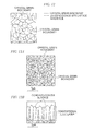
- FIG. 3A is a schematic view showing a flat-plate polygonal crystal grain structure obtained by observing an upper layer composed of a reformed AlTiO layer of coated tools A1 to A9 of the present invention, using a field-emission-type scanning electron microscope in a plane perpendicular to a layer thickness direction.
- FIG. 3B is a schematic view showing a crystal grain structure having a substantially flat layer surface and having an elongated shape in the layer thickness direction, which is obtained by observation using the field-emission-type scanning electron microscope in a plane parallel to the layer thickness direction.
- FIG. 3C is a schematic view showing a flat hexagonal crystal grain structure which is obtained by observing an upper layer composed of a reformed AlTiO layer of coated tools A10 to A15 of the present invention, using the field-emission-type scanning electron microscope in the plane perpendicular to the layer thickness direction.
- FIG. 4 is a grain boundary analysis view in the plane perpendicular to the layer thickness direction, which is obtained by measuring the upper layer composed of the reformed AlTiO layer of the coated tools A1 to A9 of the present invention, using the field-emission-type scanning electron microscope and an electronic backscattering diffraction image apparatus, showing a flat-plate polygonal grain boundary observed by the field-emission-type scanning electron microscope in a solid line, and showing a ⁇ 3 coincidence site lattice interface within the crystal grain measured by the electronic backscattering diffraction image apparatus in a broken line.
- FIG. 5A is a schematic view showing a polygonal crystal grain structure which is obtained by observing an upper layer composed of a conventional AlTiO layer of the comparative coated tools A1 to A10, using the field-emission-type scanning electron microscope in the plane perpendicular to the layer thickness direction.
- FIG. 5B is a schematic view showing a crystal grain structure having pyramidal concaves and convexes on the layer surface and having an elongated shape in the layer thickness direction, which is obtained by observation using the field-emission-type scanning electron microscope in the plane parallel to the layer thickness direction.
- FIG. 6 is a tilt angle frequency distribution graph of the (0001) plane of a reformed ⁇ -type Al 2 O 3 layer which constitutes an intermediate layer of a hard coating layer of a coated tool of the present invention.
- FIG. 7A is a schematic view showing a flat-plate polygonal crystal grain structure obtained by observing an upper layer composed of a reformed AlYO layer of coated tools B1 to B9 of the present invention, using the field-emission-type scanning electron microscope in the plane perpendicular to the layer thickness direction.
- FIG. 7B is a schematic view showing a crystal grain structure having a substantially flat layer surface and having an elongated shape in the layer thickness direction, which is obtained by observation using the field-emission-type scanning electron microscope in the plane parallel to the layer thickness direction.
- FIG. 7C is a schematic view showing a flat hexagonal crystal grain structure obtained by observing an upper layer composed of a reformed AlYO layer of coated tools B10 to B15 of the present invention, using the field-emission-type scanning electron microscope in the plane perpendicular to the layer thickness direction.
- FIG. 8 is a grain boundary analysis view in the plane perpendicular to the layer thickness direction, which is obtained by measuring the upper layer composed of the reformed AlYO layer of the coated tools B1 to B9 of the present invention, using the field-emission-type scanning electron microscope and the electronic backscattering diffraction image apparatus, showing a flat-plate polygonal grain boundary observed by the field-emission-type scanning electron microscope in a solid line, and showing a ⁇ 3 coincidence site lattice interface within the crystal grain measured by the electronic backscattering diffraction image apparatus in a broken line.
- FIG. 9A is a schematic view showing a polygonal crystal grain structure which is obtained by observing an upper layer composed of a conventional AlYO layer of the comparative coated tools B1 to B10, using the field-emission-type scanning electron microscope in the plane perpendicular to the layer thickness direction.
- FIG. 9B is a schematic view showing a crystal grain structure having pyramidal concaves and convexes on the layer surface and having an elongated shape in the layer thickness direction, which is obtained by observation using the field-emission-type scanning electron microscope in the plane parallel to the layer thickness direction.
- FIG. 10 is a tilt angle frequency distribution graph of the (0001) plane of a reformed ⁇ -type Al 2 O 3 layer which constitutes an intermediate layer of the hard coating layer of the coated tool C14 of the present invention.
- FIG. 11A is a schematic view showing a flat-plate polygonal crystal grain structure obtained by observing an upper layer composed of a reformed AlZrO layer of the coated tool C1 of the present invention, using the field-emission-type scanning electron microscope in the plane perpendicular to the layer thickness direction.
- FIG. 11B is a schematic view showing a crystal grain structure having a substantially flat layer surface and having an elongated shape in the layer thickness direction, which is obtained by observation using the field-emission-type scanning electron microscope in the plane parallel to the layer thickness direction.
- FIG. 11C is a schematic view showing a flat hexagonal crystal grain structure obtained by observing an upper layer composed of a reformed AlZrO layer of the coated tool C11 of the present invention, using the field-emission-type scanning electron microscope in the plane perpendicular to the layer thickness direction.
- FIG. 12 is a grain boundary analysis view in the plane perpendicular to the layer thickness direction, which is obtained by measuring the upper layer composed of the reformed AlZrO layer of the coated tool C1 of the present invention, using the field-emission-type scanning electron microscope and the electronic backscattering diffraction image apparatus, showing a flat-plate polygonal grain boundary observed by the field-emission-type scanning electron microscope in a solid line, and showing a ⁇ 3 coincidence site lattice interface within the crystal grain measured by the electronic backscattering diffraction image apparatus in a broken line.
- FIG. 13A is a schematic view showing a polygonal crystal grain structure obtained by observing an upper layer composed of a conventional AlZrO layer of the comparative coated tool C1, using the field-emission-type scanning electron microscope in the plane perpendicular to the layer thickness direction.
- FIG. 13B is a schematic view showing a crystal grain structure having pyramidal concaves and convexes on the layer surface and having an elongated shape in the layer thickness direction, which is obtained by observation using the field-emission-type scanning electron microscope in the plane parallel to the layer thickness direction.
- FIG. 14 is a tilt angle frequency distribution graph of the (0001) plane of a reformed Al 2 O 3 layer which constitutes an intermediate layer of a hard coating layer of the coated tool D6 of the present invention.
- FIG. 15A is a schematic view showing a flat-plate polygonal crystal grain structure which is obtained by observing an upper layer composed of a reformed Cr-containing Al 2 O 3 layer of the coated tool D1 of the present invention, using a field emission type scanning electron microscope in a plane perpendicular to a layer thickness direction.
- FIG. 15B is a schematic view showing a crystal grain structure having a substantially flat layer surface and having an elongated shape in the layer thickness direction, which is obtained by observation using the field-emission-type scanning electron microscope in the plane parallel to the layer thickness direction.
- FIG. 15C is a schematic view showing a flat hexagonal crystal grain structure which is obtained by observing an upper layer composed of a reformed Cr-containing Al 2 O 3 layer of the coated tool D11 of the present invention, using a field emission type scanning electron microscope in a plane perpendicular to a layer thickness direction.
- FIG. 16 is a grain boundary analysis view in the plane perpendicular to the layer thickness direction, which is obtained by measuring the upper layer composed of the reformed Cr-containing Al 2 O 3 layer of the coated tool D1 of the present invention, using the field-emission-type scanning electron microscope and an electronic backscattering diffraction image apparatus, showing a flat-plate polygonal grain boundary observed by the field-emission-type scanning electron microscope in a solid line, and showing a ⁇ 3 coincidence site lattice interface within the crystal grain measured by the electronic backscattering diffraction image apparatus in a broken line.
- FIG. 17A is a schematic view showing a polygonal crystal grain structure which is obtained by observing an upper layer composed of a conventional Cr-containing Al 2 O 3 layer of the conventional coated tool 1, using a field emission type scanning electron microscope in a plane perpendicular to a layer thickness direction.
- FIG. 17B is a schematic view showing a crystal grain structure having pyramidal concaves and convexes on the layer surface and having an elongated shape in the layer thickness direction, which is obtained by observation using the field-emission-type scanning electron microscope in the plane parallel to the layer thickness direction.
- FIG. 18 is an enlarged sectional schematic view showing one embodiment of a surface-coated cutting tool of the present invention.
- FIG. 18 is an enlarged sectional schematic view showing a surface-coated cutting tool 10 which is one embodiment of the present invention.
- reference numeral 11 is, for example, a body of a cutting insert or the like, and a hard coating layer 12 obtained by forming a lower layer 12 A, an intermediate layer 12 B, and an upper layer 12 C in order, is formed on the overall surface of the tool substrate 11 .
- the configuration of each part will be described below.
- the shape of the tool substrate 11 is appropriately set in conformity with the shape of a tool to which the invention is to be applied, and is not limited in the invention. Each embodiment will be described below.
- the conventional ⁇ -type Al 2 O 3 layer in the conventional coated tool 1 is vapor-deposited, for example, using a normal chemical vapor deposition apparatus under the following conditions.
- composition of reaction gas in vol. %, 6 to 10% of AlCl 3 , 10 to 15% of CO 2 , 3 to 5% of HCl, 0.05 to 0.2% of H 2 S, and H 2 as balance
- Reaction atmosphere temperature 1020 to 1050° C.
- the ⁇ -type Al 2 O 3 layer in the present invention corresponding to the intermediate layer 12 B is formed, using a normal chemical vapor deposition apparatus under the following conditions.
- composition of reaction gas in vol. %, 3 to 10% of AlCl 3 , 0.5 to 3% of CO 2 , 0.01 to 0.3% of C 2 H 4 , and H 2 as balance
- Reaction atmosphere temperature 750 to 900° C.
- Al 2 O 3 neclear is formed on the surface of a Ti compound layer which is the lower layer 12 A under the low-temperature condition described above.
- the Al 2 O 3 neclear is an Al 2 O 3 neclear thin film having a mean layer thickness of 20 to 200 nm.
- the Al 2 O 3 neclear thin film is heat treated in a condition where the reaction atmosphere is substituted to a hydrogen atmosphere of pressure: 3 to 13 kPa, and the reaction atmosphere temperature is increased to 1100 to 1200° C.
- the ⁇ -type Al 2 O 3 layer which serves as the hard coating layer, is formed under a conventional condition.
- the resulting ⁇ -type Al 2 O 3 layer (hereinafter referred to as a reformed ⁇ -type Al 2 O 3 layer), which is vapor-deposited on the heat-treated neclear thin film, is analyzed with a field emission type scanning electron microscope as schematically represented in FIGS. 1A and 1B .
- a field emission type scanning electron microscope as schematically represented in FIGS. 1A and 1B .
- individual crystal grains having a hexagonal crystal lattice present within the measurement range of a polished surface are irradiated by an electron beam.
- a tilt angle which is the angle formed between the normal line to the (0001) plane of the crystal grain and the normal line to the polished surface of the cutting tool, is measured.
- the measured tilt angles belonging to a range of 0 to 45° are sectioned every pitch of 0.25°, and the frequencies existing in each section are collected, being represented by a tilt angle frequency distribution graph.
- a tilt angle frequency distribution graph As shown in FIG. 2 , as an example, a sharp highest peak appears at a specific section of the tilt angle. Based on trial findings, it was found that the highest peak falls inside a tilt angle division ranging 0 to 10° and the total sum of frequencies existing in the range of 0 to 10° occupies a ratio of 45% or more of the total frequencies in the tilt-angle frequency distribution graph, when the atmosphere pressure of the chemical vapor deposition apparatus is kept between 5 and 8 KPa.
- (b) Forming the hard coating layer is further proceeded on the reformed ⁇ -type Al 2 O 3 layer described above, as the intermediate layer 12 B.
- a Ti-containing aluminum oxide layer having an ⁇ -type crystal structure in a chemically vapor-deposited state is vapor-deposited on the intermediate layer 12 B as the upper layer 12 C.
- the lower layer 12 A composed of the Ti compound layer, the intermediate layer 12 B composed of the reformed ⁇ -type Al 2 O 3 layer, and the upper layer 12 C composed of the Ti-containing aluminum oxide layer are vapor-deposited as a hard coating layer on the surface of the tool substrate 11 . Since the coated cutting tool 10 with the configuration described above has even more superior high-temperature strength and surface properties, the coated cutting tool 10 exerts excellent chipping resistance, even under high-speed intermittent cutting conditions where high heat is generated and the cutting edges are subjected to intermittent impact loading repeatedly.
- the Ti-containing aluminum oxide layer which is the upper layer 12 C can be formed on the reformed ⁇ -type Al 2 O 3 layer, which is the intermediate layer 12 B, under the following conditions.
- first-step vapor deposition is performed for 30 minutes under the following conditions (i) to (iii).
- vapor deposition is performed under the following conditions (i) to (iii).
- a Ti-containing aluminum oxide layer (hereinafter referred to as a reformed AlTiO layer), which has an ⁇ -type crystal structure in a chemically vapor-deposited state, can be formed.
- the reformed AlTiO layer has a mean layer thickness of 1 to 15 ⁇ m, and the content ratio of the Ti component to the total amount of the Al component is 0.002 to 0.01 (as atomic ratio).
- the texture exemplified in FIG. 3C is formed.
- the volume % of TiCl 4 is set 0.05 to 0.6, the volume % of H 2 S 0 to 0.03, and the reaction atmosphere temperature 960 to 980° C. in the second step vapor deposition, for example.
- the reaction atmosphere temperature 960 to 980° C. in the second step vapor deposition for example.
- FIG. 3C when the reformed AlTiO layer is formed by the further limited condition, and is seen within the plane perpendicular to the layer thickness direction, the large-sized grains with a flat hexagonal shape are observed.
- the outer surface of the reformed AlTiO layer is substantially flat, as shown in FIG. 3B .
- the grains that have the elongated shape within the plane parallel to the layer thickness direction account for 35% or more in area ratio, in the whole surface area perpendicular to the thickness direction of the layer.
- the reformed AlTiO layer is analyzed with the field-emission-type scanning electron microscope.
- individual crystal grains having a hexagonal crystal lattice present within the measurement range of a polished surface are irradiated by an electron beam.
- a tilt angle which is the angle formed between the normal line to the (0001) plane of the crystal grain and the normal line to the polished surface of the cutting tool, is measured.
- the measured tilt angles belonging to a range of 0 to 45° are sectioned every pitch of 0.25°, and the frequencies existing in each section are collected, being represented by a tilt angle frequency distribution graph.
- the tilt-angle frequency distribution graph In the tilt-angle frequency distribution graph, a sharp highest peak appears at a specific section of the tilt angle, and the total sum of frequencies existing in the range of 0 to 10° occupies a ratio of 60% or more of the total frequencies.
- the (0001) plane orientation ratio of the reformed AlTiO layer is higher than that of the conventional AlTiO layer of the conventional coated cutting tool, resulting even more superior high-temperature strength of the reformed AlTiO layer.
- the reformed AlTiO layer is analyzed by the field-emission-type scanning electron microscope and an electronic backscattering diffraction image apparatus.
- individual crystal grains having a hexagonal crystal lattice present within the measurement range of a polished surface are irradiated by an electron beam.
- a tilt angle which is the angle formed between the normal line to the (0001) plane of the crystal grain and the normal line to the polished surface of the cutting tool, is measured.
- a crystallographic orientation relationship between the adjacent crystal lattices is calculated, and a distribution of lattice points (constituent atom sharing lattice points) is calculated.
- the constituent atom sharing lattice point is a lattice point that has a constituent atom shared by two crystal lattices forming the grain boundary at the grain boundary.
- a constituent atom sharing lattice point type in which N lattice points not sharing the constituent atom exist between the constituent atom sharing lattice points (where N is an even number of 2 or more in view of a crystal structure of corundum type hexagonal close packed crystal but does not include even numbers of 4, 8, 14, 24, and 26 when the upper limit of N is set to 28 in view of distribution frequency) is expressed as ⁇ N+1.
- the reformed AlTiO layer When the reformed AlTiO layer is observed by the field-emission-type scanning electron microscope, it is seen that the reformed AlTiO layer includes the crystal grains with the flat-plate polygonal vertically elongated shape, as shown in FIG. 4 .
- the crystal grains with the flat-plate polygonal vertically elongated shape 60% or more of them are divided by at least one of crystal lattice interface with the constituent atom sharing lattice point type expressed by ⁇ 3 (hereinafter referred as a ⁇ 3 coincidence site lattice interface) inside.
- the upper layer composed of the reformed AlTiO layer has a high (0001) plane orientation rate, and a crystal plane at the surface thereof has the same orientation as a crystal plane (for example, (0001)) within the plane perpendicular to the layer thickness direction of this layer.
- outer surface of the upper layer is formed in the shape of a flat plate which is substantially flat (as seen within the plane parallel to the layer thickness direction), and shows excellent chipping resistance due to the surface properties thereof.
- the strength within the crystal grains is increased since the ⁇ 3 coincidence site lattice interfaces are present inside the grains with the flat-plate polygonal vertically elongated shape. Therefore, the reformed AlTiO layer has excellent high-temperature hardness and high-temperature strength and shows excellent chipping resistance, compared to the conventional AlTiO layer.
- the coated tool of the present invention includes the reformed ⁇ -type Al 2 O 3 layer having a high (0001) plane orientation rate and having excellent high-temperature strength as the intermediate layer. Furthermore, the coated tool of the present invention includes the reformed AlTiO layer having excellent high-temperature hardness, high-temperature strength, and surface properties as the upper layer.
- the coated tool of the present invention has superior high-temperature hardness, heat resistance, and high-temperature strength as compared to the conventional coated tools 1 and 2. As a result, it exhibits excellent chipping resistance for a long-term use, even when the coated tool is used for high-speed intermittent cutting accompanied by high heat generation, and intermittent impact loading acts repeatedly on the cutting edge.
- the present invention has been made on the basis of the above knowledge, and the surface-coated cutting tool of the present invention includes the following configurations.
- a surface-coated cutting tool formed by vapor-depositing, on the surface of a tool substrate made of tungsten carbide-based cemented carbide or titanium carbonitride-based cermet, a hard coating layer including (a) to (c) below.
- the lower layer is a Ti compound layer composed of one or more of a titanium carbide layer, a titanium nitride layer, a titanium carbonitride layer, a titanium carboxide layer, and a titanium oxycarbonitride layer, all of which are formed by chemical vapor deposition, and having a total mean layer thickness of 3 to 20 ⁇ m.
- the intermediate layer is an aluminum oxide layer having a mean layer thickness of 1 to 5 ⁇ m and having an ⁇ -type crystal structure in a chemically vapor-deposited state.
- the upper layer is a Ti-containing aluminum oxide layer having a mean layer thickness of 2 to 15 ⁇ m and having an ⁇ -type crystal structure in a chemically vapor-deposited state.
- the intermediate layer (b) has properties indicated by a tilt-angle frequency distribution graph in which the highest peak exists in a tilt angle division ranging 0 to 10° and the total sum of frequencies existing in the range of 0 to 10° occupies a ratio of 45% or more of the total frequencies in the tilt-angle frequency distribution graph.
- the tilt-angle frequency distribution graph is obtained by utilizing a field-emission-type scanning electron microscope. Electron beams are irradiated to individual crystal grains, which has a hexagonal crystal lattice and exists in a measurement range of a polished plane. A tilt angle formed by the normal line to the polished plane and the normal line to (0001) plane as a crystal plane of the crystal grains is measured. The measured tilt angles belonging to a range of 0 to 45° every pitch of 0.25° are sectioned. The frequencies existing in each section are collected.
- the upper layer is a Ti-containing aluminum oxide layer having a texture composed of crystal grains which have a flat-plate polygonal shape within the plane perpendicular to the layer thickness direction and have an elongated shape in the layer thickness direction within the plane parallel to the layer thickness direction.
- the upper layer (c) has properties indicated by a tilt-angle frequency distribution graph in which the highest peak exists in a tilt angle division ranging 0 to 10° and the total sum of frequencies existing in the range of 0 to 10° occupies a ratio of 60% or more of the total frequencies in the tilt-angle frequency distribution graph.
- the tilt-angle frequency distribution graph is obtained by utilizing a field-emission-type scanning electron microscope. Electron beams are irradiated to individual crystal grains, which has a hexagonal crystal lattice and exists in a measurement range of a polished plane. A tilt angle formed by the normal line to the polished plane and the normal line to (0001) plane as a crystal plane of the crystal grains is measured. The measured tilt angles belonging to a range of 0 to 45° every pitch of 0.25° are sectioned. The frequencies existing in each section are collected.
- the upper layer (c) is a Ti-containing aluminum oxide layer. Electron beams are irradiated to individual crystal grains within the measurement area on the polished surface with field-emission-type scanning electron microscope and an electron backscatter diffraction imaging device. Then, angles formed by normal lines of crystal lattice faces with hexagonal crystal lattices and the normal line to the polished surface are measured. Then, based on the measurement, a crystallographic orientation relationship between the adjacent crystal lattices is calculated. Then, a distribution of lattice points (constituent atom sharing lattice points) in which constituent atoms of a crystal lattice interface sharing one constituent atom between the crystal lattices is calculated.
- the constituent atom sharing lattice point type is expressed as ⁇ N+1, where “N” represents a number of lattice points (N) without a shared constituent atom between the constituent atom sharing lattice points.
- the constituent atom sharing lattice point type is even numbers more than 2 between crystal grains having a corundum type hexagonal close-packed structure. If the maximum number of N is set to 28 in view of distribution frequency, even numbers 4, 8, 14, 24, and 26 are excluded from the option for crystal grains having hexagonal close-packed structure.
- the upper layer (c) is a Y-containing aluminum oxide layer consisted of crystal grains, 60% or more of the grains being divided within each grain by at least one or more crystal lattice interfaces with a constituent atom sharing lattice point type expressed by ⁇ 3.
- crystal grains corresponding to 35% or more of the whole surface area perpendicular to the layer thickness direction has a flat-plate polygonal shape within the plane perpendicular to the layer thickness direction and an elongated shape in the layer thickness direction within the plane parallel to the layer thickness direction.
- the surface roughness (Ra) of the upper layer (c) in the cutting tool described above ranges from 0.05 to 0.3 ⁇ m.
- the lower layer 12 A is a Ti compound layer composed of one more of titanium carbide (hereinafter, referred to as TiC) layer, a titanium nitride (hereinafter, referred to as TiN) layer, a titanium carbonitride (hereinafter, referred to as TiCN) layer, a titanium carboxide (hereinafter, referred to as TiCO) layer, and a titanium oxycarbonitride (hereinafter, referred to as TiCNO) layer.
- TiC titanium carbide
- TiN titanium nitride
- TiCN titanium carbonitride
- TiCO titanium carboxide
- TiCNO titanium oxycarbonitride
- the lower layer 12 A is basically present as a lower layer of the reformed ⁇ -type Al 2 O 3 layer which is the intermediate layer. It has superior toughness and abrasion resistance, contributing to improve high-temperature strength of the hard coating layer.
- the lower layer 12 A adheres tightly to both the tool substrate and the reformed ⁇ -type Al 2 O 3 layer, contributing an adhesive property of the hard coating layer to the tool substrate. If the total mean layer thickness is less than 3 ⁇ m, the improvements described above cannot be sufficiently obtained. On the other hand, if the total mean layer thickness exceeds 20 ⁇ m, thermal plastic deformation occurs easily, particularly when the cutting tool is used under high-speed intermittent cutting conditions where high heat is generated and a high load acts. Thermal plastic deformation causes uneven wear of the cutting tool. Accordingly, the total mean layer thickness is set to 3 to 20 ⁇ m.
- an Al 2 O 3 neclear is formed on the surface of the Ti compound layer, which is the lower layer, under the following low-temperature conditions.
- reaction gas includes 3 to 10% of AlCl 3 , 0.5 to 3% of CO 2 , 0.01 to 0.3% of C 2 H 4 in vol. %, and H 2 as balance.
- Reaction atmosphere temperature is set at 750 to 900° C.
- Reaction atmosphere pressure is set at 3 to 13 kPa.
- the Al 2 O 3 neclear is an Al 2 O 3 neclear thin film having a mean layer thickness of 20 to 200 nm.
- the reaction atmosphere is substituted with a hydrogen atmosphere with pressure of 3 to 13 kPa.
- temperature of the reaction atmosphere is increased to 1100 to 1200° C. and the Al 2 O 3 neclear thin film is heat treated.
- An ⁇ -type Al 2 O 3 layer which serves as the hard coating layer, is formed under normal conditions.
- an ⁇ -type Al 2 O 3 layer is vapor deposited on the heat-treated Al 2 O 3 neclear thin film, resulting formation of the intermediate layer 12 B.
- the reformed ⁇ -type Al 2 O 3 layer vapor deposited on the lower layer 12 A is analyzed by the field-emission-type scanning electron microscope, as shown in FIGS. 1A and 1B .
- Electron beams are irradiated to the individual grains, which has a hexagonal crystal lattice and exists in a measurement range of a polished plane.
- a tilt angle formed by the normal line to the polished plane and the normal line to (0001) plane as a crystal plane of the crystal grains is measured.
- the measured tilt angles belonging to a range of 0 to 45° every pitch of 0.25° are sectioned.
- the frequencies existing in each section are collected and a tilt-angle frequency distribution graph is plotted. In the tilt-angle frequency distribution graph, the sharp highest peak exists in a tilt angle division ranging 0 to 10°, as shown in FIG. 2 .
- the highest peak position of the measured tilt angles in the tilt angle frequency distribution graph of the reformed ⁇ -type Al 2 O 3 layer can be changed by performing heat-treatment after the formation of the Al 2 O 3 neclear (thin film) with a predetermined layer thickness.
- the total sum of frequencies existing in the range of 0 to 10° occupies a ratio of 45% or more of the total frequencies in the tilt-angle frequency distribution graph (which means the (0001) plane orientation rate is high). Accordingly, whenever the thickness of the Al 2 O 3 neclear (thin film) becomes too thin or too thick, the position of the highest peak of the measured tilt angles moves out of the range of 0 to 10°.
- the total sum of frequencies existing in the range of 0 to 10° becomes less than a ratio of 45% of the total frequencies in the tilt-angle frequency distribution graph. As a result, excellent high-temperature strength cannot be obtained.
- the reformed ⁇ -type Al 2 O 3 layer has superior high-temperature strength in addition to the excellent high-temperature hardness and heat resistance of the ⁇ -type Al 2 O 3 layer of the conventional coated tool. Furthermore, by configuring the reformed ⁇ -type Al 2 O 3 layer as an intermediate layer with a high (0001) plane orientation rate, the (0001) plane orientation rate of the reformed AlTiO layer vapor-deposited thereon can be increased. As a result, the surface properties of an upper layer composed of the reformed AlTiO layer can be improved, and high-temperature strength can be improved.
- the mean layer thickness of the intermediate layer composed of the reformed ⁇ -type Al 2 O 3 layer is less than 1 ⁇ m, the hard coating layer cannot be provided with the above characteristics of the reformed ⁇ -type Al 2 O 3 layer.
- the mean layer thickness exceeds 5 ⁇ m, high temperature generated during cutting and high load subjected to the cutting edge leads to a higher rate of occurrence of thermal plastic deformation, which causes uneven wear of the cutting tool. As a result, the cutting tool is abrased faster.
- the mean layer thickness is set to 1 to 5 ⁇ m.
- an Al component which is a constituent component of the upper layer improves the high-temperature hardness and heat resistance of the layer.
- An extremely small amount (Ti/(Al+Ti) is 0.002 to 0.01 (as an atomic ratio) in a ratio accounted for in the total amount with Al) of Ti component contained in the upper layer improves the crystal grain boundary strength of the reformed AlTiO layer, and contributes to improving the high-temperature strength of the upper layer. If the content ratio of the Ti component in the upper layer is less than 0.002, the above functions cannot be obtained.
- the content ratio of the Ti component exceeds 0.01, the grain boundary strength deteriorates as TiO 2 grains precipitate in the layer. Therefore, it is desirable that the content ratio of the Ti component (the value of the ratio of Ti/(Al+Ti)) in the upper layer accounted for in the total amount with the Al component is 0.002 to 0.01 (as an atomic ratio).
- the reformed AlTiO layer can be vapor-deposited by adjusting chemical vapor deposition conditions of the composition of a reaction gas during vapor deposition, the reaction atmosphere temperature, and the reaction atmosphere pressure as follows, for example.
- the first-step vapor deposition is performed for 30 minutes under the following conditions:
- the second-step vapor deposition is performed under the following conditions.
- FIGS. 3A and 3B When the reformed AlTiO layer is observed by the emission type scanning electron microscope, the textures shown in FIGS. 3A and 3B are observed.
- FIG. 3A the reformed AlTiO layer is viewed within the plane perpendicular to the layer thickness direction.
- the texture containing large crystal grains with a flat-plate polygonal shape is formed.
- FIG. 3B the reformed AlTiO layer is viewed within the plane parallel to the layer thickness direction.
- the outer surface of the reformed AlTiO layer is substantially flat.
- the texture containing crystal grains with elongated shape is formed (Referred as a flat-plate polygonal elongated shape crystal grain).
- the tilt angle of the normal line to the (0001) plane to the normal line to a polished surface is measured and a tilt angle frequency graph is plotted.
- the reformed AlTiO layer since the (0001) plane orientation rate of the reformed ⁇ -type Al 2 O 3 layer, which is the intermediate layer, is 45% or more, the reformed AlTiO layer is also formed as a layer having a high (0001) plane orientation rate (the (0001) plane orientation rate is 60% or more).
- the upper layer When the upper layer is viewed within the plane parallel to the layer thickness direction, the outer surface of the upper layer is formed in the shape of a substantially flat plate. Thus, the upper layer has a excellent surface property. Consequently, the upper layer shows superior chipping resistance as compared to the conventional AlTiO layer.
- the texture shown in FIG. 3C is formed.
- the texture when it is viewed within the plane perpendicular to the layer thickness direction, there are large-sized crystal grains with a flat-plate hexagonal shape.
- the outer surface of the upper layer is substantially flat and the crystal grains have an elongated shape stretched in the layer thickness direction, as shown in FIG. 3B .
- the ratio of the surface area occupied by the crystal grains having the flat-plate hexagonal elongated shape, to the whole surface area of the plane parallel to the layer thickness direction accounts for 35% or more, in the upper layer formed in the further limited conditions.
- the reformed AlTiO layer is analyzed with a field-emission-type scanning electron microscope and the electronic backscattering diffraction image apparatus.
- electron beams are irradiated to individual crystal grains within the measurement range of the polished surface.
- angles between the normal line to each of crystal lattice planes with a hexagonal crystal lattice and the normal line to the polished surface are measured. From the measurement results, the crystal orientation relationship between adjacent crystal lattices is calculated.
- distribution of lattice points (constituent atom sharing lattice points) is calculated.
- the constituent atom sharing lattice point is a lattice point that has a constituent atom shared by two crystal lattices forming the grain boundary at the grain boundary.
- a constituent atom sharing lattice point configuration is expressed by ⁇ N+1, where the number represented by N is the number of lattice points that have no constituent atom shared at the grain boundary between two constituent atom sharing lattice points with constituent atoms.
- the constituent atom sharing lattice point type is even numbers more than 2 between crystal grains having a corundum type hexagonal close-packed structure. If the maximum number of N is set to 28 in view of distribution frequency, even numbers 4, 8, 14, 24, and 26 are excluded from the option for crystal grains having hexagonal close-packed structure. As shown in FIG.
- the crystal grains of the reformed AlTiO layer are divided by at least one of ⁇ 3 coincidence site lattice interface within each crystal grain.
- the ratio of surface area occupied by the crystal grains that have the flat-plate polygonal elongated shape and divided by at least one of ⁇ 3 coincidence site lattice interface, to the surface area occupied by crystal grains with the flat-plate polygonal elongated shape (including the flat-plate hexagonal elongated shape), is 60% or more.
- the strength within the crystal grains of the reformed AlTiO layer is increased due to the presence of the ⁇ 3 coincidence site lattice interface in the crystal grains with the flat-plate polygonal (including hexagonal) elongated shape.
- cracking of the reformed AlTiO layer is suppressed during high-speed intermittent cutting work where high load is subjected to the reformed AlTiO layer. Even if the cracking occurred, growth and spreading of the cracking would be prevented. Therefore, chipping resistance, fracture resistance, and spalling resistance are improved in the cutting tool having the reformed AlTiO layer.
- the upper layer of the present invention which has a high (0001) plane orientation rate, has flat surface properties, and is composed of the reformed AlTiO layer in which the ⁇ 3 coincidence site lattice interfaces are present with in the flat-plate polygonal (including flat hexagonal) elongated crystal grains, exhibits excellent chipping resistance and abrasion resistance for a prolonged period of time without causing chipping, fracture, spalling, or the like and also without causing thermal plastic deformation, uneven wear, or the like, even in high-speed intermittent cutting work accompanied by high heat generation and high load subjected on the cutting edge.
- the layer thickness of the upper layer composed of the reformed AlTiO layer is less than 2 ⁇ m, the excellent characteristics of the upper layer cannot be sufficiently exhibited. On the other hand, if the layer thickness of the upper layer exceeds 15 ⁇ m, thermal plastic deformation, which causes uneven wear, easily occurs. In addition, a rate of occurrence of chipping is also increased. Therefore, the mean layer thickness of the upper layer is set to 2 to 15 ⁇ m.
- the conventional AlTiO layer (the layer described in the PTL 2 (Japanese Unexamined Patent Application Publication No. 2006-289556)), was analyzed by the field-emission-type scanning electron microscope and the electronic backscattering diffraction image apparatus.
- the texture of crystal grains and the constituent atom sharing lattice point configuration of the conventional AlTiO layer were analyzed.
- the texture of the crystal grains of the conventional AlTiO layer is shown in FIGS. 5A and 5B .
- the texture of the crystal grains of the conventional AlTiO layer is made of pyramidal-shaped crystal grains with a polygonal elongated shape stretched to the layer thickness direction.
- the outer surface of the conventional AlTiO layer has protuberances and recesses along with the pyramidal shape of the crystal grains. Because of these, the abrasion resistance of the conventional AlTiO layer is inferior compared to that of the reformed AlTiO layer.
- the ratio of surface area occupied by the pyramidal-shaped crystal grains, which have a polygonal elongated shape stretched to the layer thickness direction and contain a ⁇ 3 coincidence site lattice interface within, to the surface area occupied by crystal grains, which consist the conventional AlTiO layer and have the convexoconcave polygonal elongated shape stretched to the layer thickness direction is 40% or less. Therefore, the strength within the crystal grains is not improved as in the reformed AlTiO layer.
- the conventional coated tool 2 in which the upper layer of the hard coating layer is composed of the conventional AlTiO layer cannot prevent occurrence of chipping, fracture, spalling, or the like and is inferior in tool performance, in high-speed intermittent cutting work accompanied by high heat generation and intermittent impact loading subjected on the cutting edge.
- polishing processing using a grind stone or polishing processing using wet blasting can be performed on the surface of the upper layer, so that the surface roughness of the reformed AlTiO layer can be further adjusted.
- the occurrence of welding to the surface-coated tool during cutting can be suppressed by adjusting the surface roughness of the reformed AlTiO layer to Ra 0.05 to 0.3 ⁇ m.
- the surface roughness Ra in the present invention means the value of arithmetic mean roughness Ra defined by JIS B0601 (1994), and the measuring method thereof is not particularly limited.
- a coated tool of the second embodiment of the present invention has the following configuration.
- the conventional ⁇ -type Al 2 O 3 layer in the conventional coated tool 1 is vapor-deposited, for example, using a normal chemical vapor deposition apparatus under the following conditions.
- composition of reaction gas in vol. %, 6 to 10% of AlCl 3 , 10 to 15% of CO 2 , 3 to 5% of HCl, 0.05 to 0.2% of H 2 S, and H 2 as balance
- Reaction atmosphere temperature 1020 to 1050° C.
- an Al 2 O 3 neclear is formed on the surface of a Ti compound layer, which is a lower layer, using a standard chemical vapor deposition apparatus under the following low-temperature conditions: composition of reaction gas, in vol. %, 3 to 10% of AlCl 3 , 0.5 to 3% of CO 2 , 0.01 to 0.3% of C 2 H 4 , and H 2 as balance; reaction atmosphere temperature, 750 to 900° C.; reaction atmosphere pressure, 3 to 13 kPa.
- Al 2 O 3 neclear is formed on the surface of a Ti compound layer which is the lower layer 12 A under the low-temperature condition described above.
- the Al 2 O 3 neclear is an Al 2 O 3 neclear thin film having a mean layer thickness of 20 to 200 nm.
- the Al 2 O 3 neclear thin film is heat treated in a condition where the reaction atmosphere is substituted to a hydrogen atmosphere of pressure: 3 to 13 kPa, and the reaction atmosphere temperature is increased to 1100 to 1200° C.
- the ⁇ -type Al 2 O 3 layer which serves as the hard coating layer, is formed under a conventional condition.
- the resulting ⁇ -type Al 2 O 3 layer (hereinafter referred to as a reformed ⁇ -type Al 2 O 3 layer), which is vapor-deposited on the heat-treated neclear thin film, is analyzed with a field emission type scanning electron microscope as schematically represented in FIGS. 1A and 1B .
- a field emission type scanning electron microscope as schematically represented in FIGS. 1A and 1B .
- individual crystal grains having a hexagonal crystal lattice present within the measurement range of a polished surface are irradiated by an electron beam.
- a tilt angle which is the angle formed between the normal line to the (0001) plane of the crystal grain and the normal line to the polished surface of the cutting tool, is measured.
- the measured tilt angles belonging to a range of 0 to 45° are sectioned every pitch of 0.25°, and the frequencies existing in each section are collected, being represented by a tilt angle frequency distribution graph.
- a tilt angle frequency distribution graph As shown in FIG. 6 , as an example, a sharp highest peak appears at a specific section of the tilt angle. Based on trial findings, it was found that the highest peak falls inside a tilt angle division ranging 0 to 10° and the total sum of frequencies existing in the range of 0 to 10° occupies a ratio of 45% or more of the total frequencies in the tilt-angle frequency distribution graph, when the atmosphere pressure of the chemical vapor deposition apparatus is kept between 5 and 8 KPa.
- a hard coating layer is constructed by forming the reformed ⁇ -type Al 2 O 3 layer vapor-deposited under the conditions described in the above (a) as the intermediate layer, and further by vapor-depositing a Y(Yttrium)-containing aluminum oxide layer having an ⁇ -type crystal structure in a chemically vapor-deposited state as the upper layer on the intermediate layer. Then, provided is a coated tool in which the lower layer composed of the Ti compound layer, the intermediate layer composed of the reformed ⁇ -type Al 2 O 3 layer, and the upper layer composed of the Y-containing aluminum oxide layer are vapor-deposited as a hard coating layer on the surface of the tool substrate. The present inventor has found that this coated tool has superior high-temperature strength and surface properties, thereby exhibiting excellent chipping resistance, even under high-speed intermittent cutting conditions where intermittent impact load is subjected on the cutting edge.
- the Y-containing aluminum oxide layer which is the upper layer can be formed on the reformed ⁇ -type Al 2 O 3 layer, which is the intermediate layer, under the following conditions. For example, first, as a first step, first-step vapor deposition is performed for 1 hour under the following conditions (i) to (iii).
- vapor deposition is performed under the following conditions (i) to (iii).
- a Y-containing aluminum oxide layer (hereinafter referred to as a reformed AlYO layer), which has an ⁇ -type crystal structure in a chemically vapor-deposited state, can be formed.
- the reformed AlYO layer has a mean layer thickness of 1 to 15 ⁇ m, and the content ratio of the Y component to the total amount of the Al component is 0.0005 to 0.01 (as atomic ratio).
- the texture exemplified in FIG. 7C is formed.
- the volume % of YCl 3 is set 0.6 to 0.8, the volume % of H 2 S 0.25 to 0.4, and the reaction atmosphere temperature 960 to 980° C. in the second step vapor deposition, for example.
- the reaction atmosphere temperature 960 to 980° C. in the second step vapor deposition for example.
- FIG. 7C when the reformed AlYO layer is formed by the further limited condition, and is seen within the plane perpendicular to the layer thickness direction, the large-sized grains with a flat hexagonal shape are observed.
- the outer surface of the reformed AlYO layer is substantially flat, as shown in FIG. 7B .
- the grains that have the elongated shape within the plane parallel to the layer thickness direction account for 35% or more in area ratio, in the whole surface area perpendicular to the thickness direction of the layer.
- the reformed AlYO layer is analyzed with the field-emission-type scanning electron microscope.
- individual crystal grains having a hexagonal crystal lattice present within the measurement range of a polished surface are irradiated by an electron beam.
- a tilt angle which is the angle formed between the normal line to the (0001) plane of the crystal grain and the normal line to the polished surface of the cutting tool, is measured.
- the measured tilt angles belonging to a range of 0 to 45° are sectioned every pitch of 0.25°, and the frequencies existing in each section are collected, being represented by a tilt angle frequency distribution graph.
- the tilt-angle frequency distribution graph In the tilt-angle frequency distribution graph, a sharp highest peak appears at a specific section of the tilt angle, and the total sum of frequencies existing in the range of 0 to 10° occupies a ratio of 60% or more of the total frequencies.
- the (0001) plane orientation ratio of the reformed AlYO layer is higher than that of the conventional AlYO layer of the conventional coated cutting tool, resulting even more superior high-temperature strength of the reformed AlYO layer.
- the reformed AlYO layer is analyzed by the field-emission-type scanning electron microscope and an electronic backscattering diffraction image apparatus.
- individual crystal grains having a hexagonal crystal lattice present within the measurement range of a polished surface are irradiated by an electron beam.
- a tilt angle which is the angle formed between the normal line to the (0001) plane of the crystal grain and the normal line to the polished surface of the cutting tool, is measured.
- a crystallographic orientation relationship between the adjacent crystal lattices is calculated, and a distribution of lattice points (constituent atom sharing lattice points) in which constituent atoms of a crystal lattice interface sharing one constituent atom between the crystal lattices is calculated.
- a constituent atom sharing lattice point type in which N lattice points not sharing the constituent atom exist between the constituent atom sharing lattice points (where N is an even number of 2 or more in view of a crystal structure of corundum type hexagonal close packed crystal but does not include even numbers of 4, 8, 14, 24, and 26 when the upper limit of N is set to 28 in view of distribution frequency) is expressed as ⁇ N+1.
- the reformed AlYO layer When the reformed AlYO layer is observed by the field-emission-type scanning electron microscope, it is seen that the reformed AlYO layer includes the crystal grains with the flat-plate polygonal vertically elongated shape, as shown in FIG. 8 .
- the crystal grains with the flat-plate polygonal vertically elongated shape 60% or more of them are divided by at least one of crystal lattice interface with the constituent atom sharing lattice point type expressed by ⁇ 3 (hereinafter referred as a ⁇ 3 coincidence site lattice interface) in the crystal grains.
- the upper layer composed of the reformed AlYO layer has a high (0001) plane orientation rate, and a crystal plane at the surface thereof has the same orientation as a crystal plane (for example, (0001)) within the plane perpendicular to the layer thickness direction of this layer.
- outer surface of the upper layer is formed in the shape of a flat plate which is substantially flat (as seen within the plane parallel to the layer thickness direction), and shows excellent chipping resistance due to the surface properties thereof.
- the strength within the crystal grains is increased since the ⁇ 3 coincidence site lattice interfaces are present inside the grains with the flat-plate polygonal vertically elongated shape. Therefore, the reformed AlYO layer has excellent high-temperature hardness and high-temperature strength and shows excellent chipping resistance, compared to the conventional AlYO layer.
- the coated tool of the present invention includes the reformed ⁇ -type Al 2 O 3 layer having a high (0001) plane orientation rate and having excellent high-temperature strength as the intermediate layer. Furthermore, the coated tool of the present invention includes the reformed AlYO layer having excellent high-temperature hardness, high-temperature strength, and surface properties as the upper layer.
- the coated tool of the present invention has superior high-temperature hardness, heat resistance, and high-temperature strength as compared to the conventional coated tools 1 and 2. As a result, it exhibits excellent chipping resistance for a long-term use, even when the coated tool is used for high-speed intermittent cutting accompanied by high heat generation, and intermittent impact loading acts repeatedly on the cutting blade.
- the second embodiment of the present invention has been made on the basis of the above knowledge, and the surface-coated cutting tool of the present invention includes the following configurations.
- a surface-coated cutting tool formed by vapor-depositing, on the surface of a tool substrate made of tungsten carbide-based cemented carbide or titanium carbonitride-based cermet, a hard coating layer including the above (a) to (c).
- the lower layer is a Ti compound layer composed of one or more of a titanium carbide layer, a titanium nitride layer, a titanium carbonitride layer, a titanium carboxide layer, and a titanium oxycarbonitride layer, all of which are formed by chemical vapor deposition, and having a total mean layer thickness of 3 to 20 ⁇ m.
- the intermediate layer is an aluminum oxide layer having a mean layer thickness of 1 to 5 ⁇ m and having an ⁇ -type crystal structure in a chemically vapor-deposited state.
- the upper layer is a Y-containing aluminum oxide layer having a mean layer thickness of 2 to 15 ⁇ m and having an ⁇ -type crystal structure in a chemically vapor-deposited state.
- the intermediate layer (b) has properties indicated by a tilt-angle frequency distribution graph in which the highest peak exists in a tilt angle division ranging 0 to 10° and the total sum of frequencies existing in the range of 0 to 10° occupies a ratio of 45% or more of the total frequencies in the tilt-angle frequency distribution graph.
- the tilt-angle frequency distribution graph is obtained by utilizing a field-emission-type scanning electron microscope. Electron beams are irradiated to individual crystal grains, which has a hexagonal crystal lattice and exists in a measurement range of a polished plane. A tilt angle formed by the normal line to the polished plane and the normal line to (0001) plane as a crystal plane of the crystal grains is measured. The measured tilt angles belonging to a range of 0 to 45° every pitch of 0.25° are sectioned. The frequencies existing in each section are collected.
- the upper layer is a Y-containing aluminum oxide layer having a texture composed of crystal grains which have a flat-plate polygonal shape within the plane perpendicular to the layer thickness direction and have an elongated shape in the layer thickness direction within the plane parallel to the layer thickness direction.
- the upper layer (c) has properties indicated by a tilt-angle frequency distribution graph in which the highest peak exists in a tilt angle division ranging 0 to 10° and the total sum of frequencies existing in the range of 0 to 10° occupies a ratio of 60% or more of the total frequencies in the tilt-angle frequency distribution graph.
- the tilt-angle frequency distribution graph is obtained by utilizing a field-emission-type scanning electron microscope. Electron beams are irradiated to individual crystal grains, which has a hexagonal crystal lattice and exists in a measurement range of a polished plane. A tilt angle formed by the normal line to the polished plane and the normal line to (0001) plane as a crystal plane of the crystal grains is measured. The measured tilt angles belonging to a range of 0 to 45° every pitch of 0.25° are sectioned. The frequencies existing in each section are collected.
- the upper layer (c) is a Y-containing aluminum oxide layer. Electron beams are irradiated to individual crystal grains within the measurement area on the polished surface with field-emission-type scanning electron microscope and an electron backscatter diffraction imaging device. Then, angles formed by normal lines of crystal lattice faces with hexagonal crystal lattices and the normal line to the polished surface are measured. Then, based on the measurement, a crystallographic orientation relationship between the adjacent crystal lattices is calculated. Then, a distribution of lattice points (constituent atom sharing lattice points) in which constituent atoms of a crystal lattice interface sharing one constituent atom between the crystal lattices is calculated.
- the constituent atom sharing lattice point type is expressed as ⁇ N+1, where “N” represents a number of lattice points (N) without a shared constituent atom between the constituent atom sharing lattice points.
- the constituent atom sharing lattice point type is even numbers more than 2 between crystal grains having a corundum type hexagonal close-packed structure. If the maximum number of N is set to 28 in view of distribution frequency, even numbers 4, 8, 14, 24, and 26 are excluded from the option for crystal grains having hexagonal close-packed structure.
- the upper layer (c) is a Y-containing aluminum oxide layer consisted of crystal grains, 60% or more of the grains being divided within each grain by at least one or more crystal lattice interfaces with a constituent atom sharing lattice point type expressed by ⁇ 3.
- crystal grains corresponding to 35% or more of the whole surface area perpendicular to the layer thickness direction has a flat-plate polygonal shape within the plane perpendicular to the layer thickness direction and an elongated shape in the layer thickness direction within the plane parallel to the layer thickness direction.
- the surface roughness (Ra) of the upper layer (c) in the cutting tool described above ranges from 0.05 to 0.3 ⁇ m.
- the lower layer 12 A is a Ti compound layer composed of one more of titanium carbide (hereinafter, referred to as TiC) layer, a titanium nitride (hereinafter, referred to as TiN) layer, a titanium carbonitride (hereinafter, referred to as TiCN) layer, a titanium carboxide (hereinafter, referred to as TiCO) layer, and a titanium oxycarbonitride (hereinafter, referred to as TiCNO) layer.
- TiC titanium carbide
- TiN titanium nitride
- TiCN titanium carbonitride
- TiCO titanium carboxide
- TiCNO titanium oxycarbonitride
- the lower layer 12 A is basically present as a lower layer of the reformed ⁇ -type Al 2 O 3 layer which is the intermediate layer. It has superior toughness and abrasion resistance, contributing to improve high-temperature strength of the hard coating layer.
- the lower layer 12 A adheres tightly to both the tool substrate and the reformed ⁇ -type Al 2 O 3 layer, contributing an adhesive property of the hard coating layer to the tool substrate. If the total mean layer thickness is less than 3 ⁇ m, the improvements described above cannot be sufficiently obtained. On the other hand, if the total mean layer thickness exceeds 20 ⁇ m, chipping occurs easily, particularly when the cutting tool is used under high-speed intermittent cutting conditions where high heat is generated and an intermittent load is subjected to the cutting tool. The chipping causes abnormal wear of the cutting tool. Accordingly, the total mean layer thickness is set to 3 to 20 ⁇ m.
- an Al 2 O 3 neclear is formed on the surface of the Ti compound layer, which is the lower layer, under the normal chemical vapor deposition apparatus under the following low-temperature conditions.
- composition of reaction gas in vol. %, 3 to 10% of AlCl3, 0.5 to 3% of CO 2 , 0.01 to 0.3% of C 2 H 4 , and H 2 as balance
- Reaction atmosphere temperature 750 to 900° C.
- the Al 2 O 3 neclear is an Al 2 O 3 neclear thin film having a mean layer thickness of 20 to 200 nm.
- the reaction atmosphere is substituted with a hydrogen atmosphere with pressure of 3 to 13 kPa.
- temperature of the reaction atmosphere is increased to 1100 to 1200° C. and the Al 2 O 3 neclear thin film is heat treated.
- An ⁇ -type Al 2 O 3 layer which serves as the hard coating layer, is formed under normal conditions.
- an ⁇ -type Al 2 O 3 layer is vapor deposited on the heat-treated Al 2 O 3 neclear thin film, resulting formation of the intermediate layer 12 B.
- the intermediate layer 12 is analyzed by the field-emission-type scanning electron microscope, as shown in FIGS. 1A and 1B . Electron beams are irradiated to the individual grains, which has a hexagonal crystal lattice and exists in a measurement range of a polished plane. A tilt angle formed by the normal line to the polished plane and the normal line to (0001) plane as a crystal plane of the crystal grains is measured. The measured tilt angles belonging to a range of 0 to 45° every pitch of 0.25° are sectioned. The frequencies existing in each section are collected and a tilt-angle frequency distribution graph is plotted. In the tilt-angle frequency distribution graph, the sharp highest peak exists in a tilt angle division ranging 0 to 10°, as shown in FIG. 6 .
- the highest peak position of the measured tilt angles in the tilt angle frequency distribution graph of the reformed ⁇ -type Al 2 O 3 layer can be changed by performing heat-treatment after the formation of the Al 2 O 3 neclear (thin film) with a predetermined layer thickness.
- the total sum of frequencies existing in the range of 0 to 10° occupies a ratio of 45% or more of the total frequencies in the tilt-angle frequency distribution graph (which means the (0001) plane orientation rate is high). Accordingly, whenever the thickness of the Al 2 O 3 neclear (thin film) becomes too thin or too thick, the position of the highest peak of the measured tilt angles moves out of the range of 0 to 10°.
- the total sum of frequencies existing in the range of 0 to 10° becomes less than a ratio of 45% of the total frequencies in the tilt-angle frequency distribution graph. As a result, excellent high-temperature strength cannot be obtained.
- the reformed ⁇ -type Al 2 O 3 layer has superior high-temperature strength in addition to the excellent high-temperature hardness and heat resistance of the ⁇ -type Al 2 O 3 layer of the conventional coated tool. Furthermore, by configuring the reformed ⁇ -type Al 2 O 3 layer as an intermediate layer with a high (0001) plane orientation rate, the (0001) plane orientation rate of the reformed AlYO layer vapor-deposited thereon can be increased. As a result, the surface properties of an upper layer composed of the reformed AlYO layer can be improved, and high-temperature strength can be improved.
- the mean layer thickness of the intermediate layer composed of the reformed ⁇ -type Al 2 O 3 layer is less than 1 ⁇ m, the hard coating layer cannot be provided with the above characteristics of the reformed ⁇ -type Al 2 O 3 layer.
- the mean layer thickness exceeds 5 ⁇ m, high temperature generated during cutting and an intermittent load subjected to the cutting edge leads to a higher rate of occurrence of chipping, which causes abnormal wear of the cutting tool. As a result, the cutting tool is abrased faster.
- the mean layer thickness is set to 1 to 5 ⁇ m.
- an Al component which is a constituent component of the upper layer improves the high-temperature hardness and heat resistance of the layer.
- An extremely small amount (Y/(Al+Y) is 0.0005 to 0.01 (as an atomic ratio) in a ratio accounted for in the total amount with Al) of Y component contained in the upper layer improves the crystal grain boundary strength of the reformed AlYO layer, and contributes to improving the high-temperature strength of the upper layer. If the content ratio of the Y component in the upper layer is less than 0.0005, the above functions cannot be obtained.
- the content ratio of the Y component exceeds 0.01, the grain boundary strength deteriorates as Y 2 O 3 grains precipitate in the layer. Therefore, it is desirable that the content ratio of the Y component (the value of the ratio of Y/(Al+Y)) in the upper layer accounted for in the total amount with the Al component is 0.0005 to 0.01 (as an atomic ratio).
- the reformed AlYO layer can be vapor-deposited by adjusting chemical vapor deposition conditions of the composition of a reaction gas during vapor deposition, the reaction atmosphere temperature, and the reaction atmosphere pressure as follows, for example.
- the first-step vapor deposition is performed for 1 hour under the following conditions:
- the second-step vapor deposition is performed under the following conditions.
- FIGS. 7A and 7B When the reformed AlYO layer is observed by the emission type scanning electron microscope, the textures shown in FIGS. 7A and 7B are observed.
- FIG. 7A the reformed AlTiO layer is viewed within the plane perpendicular to the layer thickness direction.
- the texture containing large crystal grains with a flat-plate polygonal shape is formed.
- FIG. 7B the reformed AlYO layer is viewed within the plane parallel to the layer thickness direction.
- the outer surface of the reformed AlYO layer is substantially flat.
- the texture containing crystal grains with elongated shape is formed (Referred as a flat-plate polygonal elongated shape crystal grain).
- the tilt angle of the normal line to the (0001) plane to the normal line to a polished surface is measured and a tilt angle frequency graph is plotted.
- the reformed AlYO layer since the (0001) plane orientation rate of the reformed ⁇ -type Al 2 O 3 layer, which is the intermediate layer, is 45% or more, the reformed AlYO layer is also formed as a layer having a high (0001) plane orientation rate (the (0001) plane orientation rate is 60% or more).
- the upper layer When the upper layer is viewed within the plane parallel to the layer thickness direction, the outer surface of the upper layer is formed in the shape of a substantially flat plate. Thus, the upper layer has a excellent surface property. Consequently, the upper layer shows superior chipping resistance as compared to the conventional AlYO layer.
- the vapor deposition of the reformed AlYO layer is performed under further limited conditions (for example, the conditions where volume percentage of H 2 S in the reaction gas is 0.5 to 0.75 vol. %, and the reaction atmosphere temperature is set to 1020 to 1030° C., in the first-step vapor deposition, and volume percentages of YCl 3 and H 2 S in the reaction gas are 0.6 to 0.8 vol. % and 0.25 to 0.4 vol %, respectively, and the reaction atmosphere temperature is set to 960 to 980° C., in the second-step vapor deposition), the texture shown in FIG. 7C is formed.
- the reaction atmosphere temperature is set to 960 to 980° C.
- the texture when it is viewed within the plane perpendicular to the layer thickness direction, there are large-sized crystal grains with a flat-plate hexagonal shape.
- the outer surface of the upper layer is substantially flat and the crystal grains have an elongated shape stretched in the layer thickness direction, as shown in FIG. 7B .
- the ratio of the surface area occupied by the crystal grains having the flat-plate hexagonal elongated shape, to the whole surface area of the plane parallel to the layer thickness direction accounts for 35% or more, in the upper layer formed in the further limited conditions.
- the reformed AlYO layer is analyzed with a field-emission-type scanning electron microscope and the electronic backscattering diffraction image apparatus.
- electron beams are irradiated to individual crystal grains within the measurement range of the polished surface.
- angles between the normal line to each of crystal lattice planes with a hexagonal crystal lattice and the normal line to the polished surface are measured. From the measurement results, the crystal orientation relationship between adjacent crystal lattices is calculated.
- distribution of lattice points (constituent atom sharing lattice points) is calculated.
- the constituent atom sharing lattice point is a lattice point that has a constituent atom shared by two crystal lattices forming the grain boundary at the grain boundary.
- a constituent atom sharing lattice point configuration is expressed by ⁇ N+1, where the number represented by N is the number of lattice points that have no constituent atom shared at the grain boundary between two constituent atom sharing lattice points with constituent atoms.
- the constituent atom sharing lattice point type is even numbers more than 2 between crystal grains having a corundum type hexagonal close-packed structure. If the maximum number of N is set to 28 in view of distribution frequency, even numbers 4, 8, 14, 24, and 26 are excluded from the option for crystal grains having hexagonal close-packed structure. As shown in FIG.
- the crystal grains of the reformed AlYO layer are divided by at least one of ⁇ 3 coincidence site lattice interface within each crystal grain.
- the ratio of surface area occupied by the crystal grains that have the flat-plate polygonal elongated shape and divided by at least one of ⁇ 3 coincidence site lattice interface, to the surface area occupied by crystal grains with the flat-plate polygonal elongated shape (including the flat-plate hexagonal elongated shape), is 60% or more.
- the strength within the crystal grains of the reformed AlYO layer is increased due to the presence of the ⁇ 3 coincidence site lattice interface in the crystal grains with the flat-plate polygonal (including hexagonal) elongated shape.
- cracking of the reformed AlYO layer is suppressed during high-speed intermittent cutting work where high load is subjected to the reformed AlYO layer. Even if the cracking occurred, growth and spreading of the cracking would be prevented. Therefore, chipping resistance, fracture resistance, and spalling resistance are improved in the cutting tool having the reformed AlYO layer.
- the upper layer of the present invention which has a high (0001) plane orientation rate, has flat surface properties, and is composed of the reformed AlYO layer in which the ⁇ 3 coincidence site lattice interfaces are present with in the flat-plate polygonal (including flat hexagonal) elongated crystal grains, exhibits excellent chipping resistance and abrasion resistance for a prolonged period of time without causing chipping, fracture, spalling, or the like and also without causing uneven wear, or the like, even in high-speed intermittent cutting work accompanied by high heat generation and intermittent load subjected on the cutting edge.
- the mean layer thickness of the upper layer is set to 2 to 15 ⁇ m.
- the conventional AlYO layer (the layer described in the PTL 4), was analyzed by the field-emission-type scanning electron microscope and the electronic backscattering diffraction image apparatus.
- the texture of crystal grains and the constituent atom sharing lattice point configuration of the conventional AlYO layer were analyzed.
- the texture of the crystal grains of the conventional AlYO layer is shown in FIGS. 9A and 9B .
- the texture of the crystal grains of the conventional AlYO layer is made of pyramidal-shaped crystal grains with a polygonal elongated shape stretched to the layer thickness direction.
- the outer surface of the conventional AlYO layer has protuberances and recesses along with the pyramidal shape of the crystal grains.
- the abrasion resistance of the conventional AlYO layer is inferior compared to that of the reformed AlYO layer.
- the ratio of surface area occupied by the pyramidal-shaped crystal grains, which have a polygonal elongated shape stretched to the layer thickness direction and contain a ⁇ 3 coincidence site lattice interface within, to the surface area occupied by crystal grains, which consist the conventional AlYO layer and have the convexoconcave polygonal elongated shape stretched to the layer thickness direction is 40% or less. Therefore, the strength within the crystal grains is not improved as in the reformed AlYO layer.
- the conventional coated tool 2 in which the upper layer of the hard coating layer is composed of the conventional AlYO layer cannot prevent occurrence of chipping, fracture, spalling, or the like and is inferior in tool performance, in high-speed intermittent cutting work accompanied by high heat generation and repeated intermittent impact loading subjected on the cutting edge. In addition, uneven wear or the like occurs in the conventional coated tool 2.
- polishing processing using a grind stone or polishing processing using wet blasting can be performed on the surface of the upper layer, so that the surface roughness of the reformed AlYO layer can be further adjusted.
- the occurrence of welding to the surface-coated tool during cutting can be suppressed by adjusting the surface roughness of the reformed AlYO layer to Ra 0.05 to 0.3 ⁇ m.
- the surface roughness Ra in the present invention means the value of arithmetic mean roughness Ra defined by JIS B0601 (1994), and the measuring method thereof is not particularly limited.
- a third embodiment of the present invention includes the following aspects.
- the conventional ⁇ -type Al 2 O 3 layer in the conventional coated tool 1 is vapor-deposited, for example, using a normal chemical vapor deposition apparatus under the following conditions.
- composition of reaction gas in vol. %, 6 to 10% of AlCl 3 , 10 to 15% of CO 2 , 3 to 5% of HCl, 0.05 to 0.2% of H 2 S, and H 2 as balance
- Reaction atmosphere temperature 1020 to 1050° C.
- the ⁇ -type Al 2 O 3 layer in the present invention corresponding to the intermediate layer is formed, using a normal chemical vapor deposition apparatus under the following low-temperature conditions.
- composition of reaction gas in vol. %, 3 to 10% of AlCl 3 , 0.5 to 3% of CO 2 , 0.01 to 0.3% of C 2 H 4 , and H 2 as balance
- Reaction atmosphere temperature 750 to 900° C.
- the Al 2 O 3 neclear is an Al 2 O 3 neclear thin film having a mean layer thickness of 20 to 200 nm.
- the Al 2 O 3 neclear thin film is heat treated in a condition where the reaction atmosphere is substituted to a hydrogen atmosphere of pressure: 3 to 13 kPa, and the reaction atmosphere temperature is increased to 1100 to 1200° C.
- the ⁇ -type Al 2 O 3 layer, which serves as the hard coating layer is formed under a conventional condition.
- the resulting reformed ⁇ -type Al 2 O 3 layer (hereinafter referred to as a reformed ⁇ -type Al 2 O 3 layer), which is vapor-deposited on the heat-treated neclear thin film, is analyzed with a field emission type scanning electron microscope as schematically represented in FIGS. 1A and 1B .
- a field emission type scanning electron microscope as schematically represented in FIGS. 1A and 1B .
- individual crystal grains having a hexagonal crystal lattice present within the measurement range of a polished surface are irradiated by an electron beam.
- a tilt angle which is the angle formed between the normal line to the (0001) plane of the crystal grain and the normal line to the polished surface of the cutting tool, is measured.
- the measured tilt angles belonging to a range of 0 to 45° are sectioned every pitch of 0.25°, and the frequencies existing in each section are collected, being represented by a tilt angle frequency distribution graph.
- a tilt angle frequency distribution graph As shown in FIG. 10 , as an example, a sharp highest peak appears at a specific section of the tilt angle. Based on trial findings, it was found that the highest peak falls inside a tilt angle division ranging 0 to 10° and the total sum of frequencies existing in the range of 0 to 10° occupies a ratio of 45% or more of the total frequencies in the tilt-angle frequency distribution graph, when the atmosphere pressure of the chemical vapor deposition apparatus is kept between 5 and 8 KPa.
- (b) Forming the hard coating layer is further proceeded on the reformed ⁇ -type Al 2 O 3 layer described above, as the intermediate layer.
- a Zr-containing aluminum oxide layer having an ⁇ -type crystal structure in a chemically vapor-deposited state is vapor-deposited on the intermediate layer as the upper layer.
- the lower layer composed of the Ti compound layer, the intermediate layer composed of the reformed ⁇ -type Al 2 O 3 layer, and the upper layer composed of the Zr-containing aluminum oxide layer are vapor-deposited as a hard coating layer on the surface of the tool substrate.
- the coated cutting tool with the configuration described above has even more superior high-temperature strength and surface properties.
- the coated cutting tool exerts excellent chipping resistance and abrasion resistance, even under high-speed intermittent cutting conditions where high heat is generated and the cutting edges are subjected to intermittent impact loading repeatedly.
- the Zr-containing aluminum oxide layer can be formed on the reformed ⁇ -type Al 2 O 3 layer, under the following conditions.
- vapor deposition is performed under the following conditions (i) to (iii).
- a Zr-containing aluminum oxide layer (hereinafter referred to as a reformed AlZrO layer), which has an ⁇ -type crystal structure in a chemically vapor-deposited state, can be formed.
- the reformed AlZrO layer has a mean layer thickness of 2 to 15 ⁇ m, and the content ratio of the Zr component to the total amount of the Al component is 0.002 to 0.01 (as atomic ratio).
- the texture exemplified in FIG. 11C is formed.
- the volume % of H 2 S is set 0.50 to 0.75, and the reaction atmosphere temperature 1020 to 1030° C. in the first step vapor deposition, and the volume % of ZrCl 4 is set 0.6 to 0.9, the volume % of H 2 S 0.25 to 0.4, and the reaction atmosphere temperature 960 to 980° C. in the second step vapor deposition, for example.
- the volume % of H 2 S is set 0.50 to 0.75
- the volume % of ZrCl 4 is set 0.6 to 0.9, the volume % of H 2 S 0.25 to 0.4, and the reaction atmosphere temperature 960 to 980° C. in the second step vapor deposition, for example.
- the reformed AlZrO layer is analyzed with the field-emission-type scanning electron microscope.
- individual crystal grains having a hexagonal crystal lattice present within the measurement range of a polished surface are irradiated by an electron beam.
- a tilt angle which is the angle formed between the normal line to the (0001) plane of the crystal grain and the normal line to the polished surface of the cutting tool, is measured.
- the measured tilt angles belonging to a range of 0 to 45° are sectioned every pitch of 0.25°, and the frequencies existing in each section are collected, being represented by a tilt angle frequency distribution graph.
- the reformed AlZrO layer is analyzed by the field-emission-type scanning electron microscope and an electronic backscattering diffraction image apparatus.
- individual crystal grains having a hexagonal crystal lattice present within the measurement range of a polished surface are irradiated by an electron beam.
- a tilt angle which is the angle formed between the normal line to the (0001) plane of the crystal grain and the normal line to the polished surface of the cutting tool, is measured.
- a crystallographic orientation relationship between the adjacent crystal lattices is calculated, and a distribution of lattice points (constituent atom sharing lattice points) is calculated.
- the constituent atom sharing lattice point is a lattice point that has a constituent atom shared by two crystal lattices forming the grain boundary at the grain boundary.
- a constituent atom sharing lattice point type in which N lattice points not sharing the constituent atom exist between the constituent atom sharing lattice points (where N is an even number of 2 or more in view of a crystal structure of corundum type hexagonal close packed crystal but does not include even numbers of 4, 8, 14, 24, and 26 when the upper limit of N is set to 28 in view of distribution frequency) is expressed as ⁇ N+1.
- the reformed AlZrO layer When the reformed AlZrO layer is observed by the field-emission-type scanning electron microscope, it is seen that the reformed AlZrO layer includes the crystal grains with the flat-plate polygonal vertically elongated shape, as shown in FIG. 12 .
- the crystal grains with the flat-plate polygonal vertically elongated shape 60% or more of them are divided by at least one of crystal lattice interface with the constituent atom sharing lattice point type expressed by ⁇ 3 (hereinafter referred as a ⁇ 3 coincidence site lattice interface) inside.
- the upper layer composed of the reformed AlZrO layer has a high (0001) plane orientation rate, and a crystal plane at the surface thereof has the same orientation as a crystal plane (for example, (0001)) within the plane perpendicular to the layer thickness direction of this layer.
- outer surface of the upper layer is formed in the shape of a flat plate which is substantially flat (as seen within the plane parallel to the layer thickness direction), and shows excellent chipping resistance due to the surface properties thereof.
- the strength within the crystal grains is increased since the ⁇ 3 coincidence site lattice interfaces are present inside the grains with the flat-plate polygonal vertically elongated shape. Therefore, the reformed AlZrO layer has excellent high-temperature hardness and high-temperature strength and shows excellent chipping resistance, compared to the conventional AlZrO layer.
- the coated tool of the present invention includes the reformed ⁇ -type Al 2 O 3 layer having a high (0001) plane orientation rate and having excellent high-temperature strength as the intermediate layer. Furthermore, the coated tool of the present invention includes the reformed AlZrO layer having excellent high-temperature hardness, high-temperature strength, and surface properties as the upper layer. The coated tool of the present invention has superior high-temperature hardness, heat resistance, and high-temperature strength as compared to the conventional coated tools 1 and 2.
- the present invention has been made on the basis of the above knowledge, and the surface-coated cutting tool of the present invention includes the following configurations.
- a surface-coated cutting tool formed by vapor-depositing, on the surface of a tool substrate made of tungsten carbide-based cemented carbide or titanium carbonitride-based cermet, a hard coating layer including the following (a) to (c).
- the lower layer is a Ti compound layer composed of one or more of a titanium carbide layer, a titanium nitride layer, a titanium carbonitride layer, a titanium carboxide layer, and a titanium oxycarbonitride layer, all of which are formed by chemical vapor deposition, and having a total mean layer thickness of 3 to 20 ⁇ m.
- the intermediate layer is an aluminum oxide layer having a mean layer thickness of 1 to 5 ⁇ m and having an ⁇ -type crystal structure in a chemically vapor-deposited state.
- the upper layer is a Zr-containing aluminum oxide layer having a mean layer thickness of 2 to 15 ⁇ m and having an ⁇ -type crystal structure in a chemically vapor-deposited state.
- the intermediate layer (b) has properties indicated by a tilt-angle frequency distribution graph in which the highest peak exists in a tilt angle division ranging 0 to 10° and the total sum of frequencies existing in the range of 0 to 10° occupies a ratio of 45% or more of the total frequencies in the tilt-angle frequency distribution graph.
- the tilt-angle frequency distribution graph is obtained by utilizing a field-emission-type scanning electron microscope. Electron beams are irradiated to individual crystal grains, which has a hexagonal crystal lattice and exists in a measurement range of a polished plane. A tilt angle formed by the normal line to the polished plane and the normal line to (0001) plane as a crystal plane of the crystal grains is measured. The measured tilt angles belonging to a range of 0 to 45° every pitch of 0.25° are sectioned. The frequencies existing in each section are collected.
- the upper layer is a Zr-containing aluminum oxide layer having a texture composed of crystal grains which have a flat-plate polygonal shape within the plane perpendicular to the layer thickness direction and have an elongated shape in the layer thickness direction within the plane parallel to the layer thickness direction.
- the upper layer (c) has properties indicated by a tilt-angle frequency distribution graph in which the highest peak exists in a tilt angle division ranging 0 to 10° and the total sum of frequencies existing in the range of 0 to 10° occupies a ratio of 60% or more of the total frequencies in the tilt-angle frequency distribution graph.
- the tilt-angle frequency distribution graph is obtained by utilizing a field-emission-type scanning electron microscope. Electron beams are irradiated to individual crystal grains, which has a hexagonal crystal lattice and exists in a measurement range of a polished plane. A tilt angle formed by the normal line to the polished plane and the normal line to (0001) plane as a crystal plane of the crystal grains is measured. The measured tilt angles belonging to a range of 0 to 45° every pitch of 0.25° are sectioned. The frequencies existing in each section are collected.
- the upper layer (c) is a Zr-containing aluminum oxide layer consisted of crystal grains, 60% or more of the grains being divided within each grain by at least one or more crystal lattice interfaces with a constituent atom sharing lattice point type expressed by ⁇ 3.
- the constituent atom sharing lattice point type is expressed as ⁇ N+1, where “N” represents a number of lattice points (N) without a shared constituent atom between the constituent atom sharing lattice points.
- the constituent atom sharing lattice point type is even numbers more than 2 between crystal grains having a corundum type hexagonal close-packed structure.
- the maximum number of N is set to 28 in view of distribution frequency, even numbers 4, 8, 14, 24, and 26 are excluded from the option for crystal grains having hexagonal close-packed structure.
- electron beams are irradiated to individual crystal grains within the measurement area on the polished surface with field-emission-type scanning electron microscope and an electron backscatter diffraction imaging device. Then, angles formed by normal lines of crystal lattice faces with hexagonal crystal lattices and the normal line to the polished surface are measured. Then, based on the measurement, a crystallographic orientation relationship between the adjacent crystal lattices is calculated.
- crystal grains corresponding to 35% or more of the whole surface area perpendicular to the layer thickness direction has a flat-plate polygonal shape within the plane perpendicular to the layer thickness direction and an elongated shape in the layer thickness direction within the plane parallel to the layer thickness direction.
- the surface roughness (Ra) of the upper layer (c) in the cutting tool described above ranges from 0.05 to 0.3 ⁇ m.
- the lower layer 12 A is a Ti compound layer composed of one more of titanium carbide (hereinafter, referred to as TiC) layer, a titanium nitride (hereinafter, referred to as TiN) layer, a titanium carbonitride (hereinafter, referred to as TiCN) layer, a titanium carboxide (hereinafter, referred to as TiCO) layer, and a titanium oxycarbonitride (hereinafter, referred to as TiCNO) layer.
- TiC titanium carbide
- TiN titanium nitride
- TiCN titanium carbonitride
- TiCO titanium carboxide
- TiCNO titanium oxycarbonitride
- the lower layer 12 A is basically present as a lower layer of the reformed ⁇ -type Al 2 O 3 layer which is the intermediate layer. It has superior toughness and abrasion resistance, contributing to improve high-temperature strength of the hard coating layer.
- the lower layer 12 A adheres tightly to both the tool substrate and the reformed ⁇ -type Al 2 O 3 layer, contributing an adhesive property of the hard coating layer to the tool substrate. If the total mean layer thickness is less than 3 ⁇ m, the improvements described above cannot be sufficiently obtained. On the other hand, if the total mean layer thickness exceeds 20 ⁇ m, thermal plastic deformation occurs easily, particularly when the cutting tool is used under high-speed intermittent cutting conditions where an intermittent and blasting high loads are subjected on the cutting edge. Thermal plastic deformation causes uneven wear of the cutting tool. Accordingly, the total mean layer thickness is set to 3 to 20 ⁇ m.
- an Al 2 O 3 neclear is formed on the surface of the Ti compound layer, which is the lower layer, under the following low-temperature conditions.
- reaction gas includes 3 to 10% of AlCl 3 , 0.5 to 3% of CO 2 , 0.01 to 0.3% of C 2 H 4 in vol. %, and H 2 as balance.
- Reaction atmosphere temperature is set at 750 to 900° C.
- Reaction atmosphere pressure is set at 3 to 13 kPa.
- the Al 2 O 3 neclear is an Al 2 O 3 neclear thin film having a mean layer thickness of 20 to 200 nm.
- the reaction atmosphere is substituted with a hydrogen atmosphere with pressure of 3 to 13 kPa.
- temperature of the reaction atmosphere is increased to 1100 to 1200° C. and the Al 2 O 3 neclear thin film is heat treated.
- An ⁇ -type Al 2 O 3 layer which serves as the hard coating layer, is formed under normal conditions.
- an ⁇ -type Al 2 O 3 layer is vapor deposited on the heat-treated Al 2 O 3 neclear thin film, resulting formation of the intermediate layer.
- the reformed ⁇ -type Al 2 O 3 layer vapor deposited on the lower layer 12 A is analyzed by the field-emission-type scanning electron microscope, as shown in FIGS. 1A and 1B .
- Electron beams are irradiated to the individual grains, which has a hexagonal crystal lattice and exists in a measurement range of a polished plane.
- a tilt angle formed by the normal line to the polished plane and the normal line to (0001) plane as a crystal plane of the crystal grains is measured.
- the measured tilt angles belonging to a range of 0 to 45° every pitch of 0.25° are sectioned.
- the frequencies existing in each section are collected and a tilt-angle frequency distribution graph is plotted. In the tilt-angle frequency distribution graph, the sharp highest peak exists in a tilt angle division ranging 0 to 10°, as shown in FIG. 10 .
- the highest peak position of the measured tilt angles in the tilt angle frequency distribution graph of the reformed ⁇ -type Al 2 O 3 layer can be changed by performing heat-treatment after the formation of the Al 2 O 3 neclear (thin film) with a predetermined layer thickness.
- the total sum of frequencies existing in the range of 0 to 10° occupies a ratio of 60% or more of the total frequencies in the tilt-angle frequency distribution graph (which means the (0001) plane orientation rate is high). Accordingly, whenever the thickness of the Al 2 O 3 neclear (thin film) becomes too thin or too thick, the position of the highest peak of the measured tilt angles moves out of the range of 0 to 10°.
- the total sum of frequencies existing in the range of 0 to 10° becomes less than a ratio of 60% of the total frequencies in the tilt-angle frequency distribution graph. As a result, excellent high-temperature strength cannot be obtained.
- the reformed ⁇ -type Al 2 O 3 layer has superior high-temperature strength in addition to the excellent high-temperature hardness and heat resistance of the ⁇ -type Al 2 O 3 layer of the conventional coated tool. Furthermore, by configuring the reformed ⁇ -type Al 2 O 3 layer as an intermediate layer with a high (0001) plane orientation rate, the (0001) plane orientation rate of the reformed AlZrO layer vapor-deposited thereon can be increased. As a result, the surface properties of an upper layer composed of the reformed AlZrO layer can be improved, and high-temperature strength can be improved.
- the mean layer thickness of the intermediate layer composed of the reformed ⁇ -type Al 2 O 3 layer is less than 1 ⁇ m, the hard coating layer cannot be provided with the above characteristics of the reformed ⁇ -type Al 2 O 3 layer.
- the mean layer thickness exceeds 5 ⁇ m, high temperature generated during cutting and an intermittent and blasting high load subjected to the cutting edge leads to a higher rate of occurrence of thermal plastic deformation, which causes uneven wear of the cutting tool. As a result, the cutting tool is abrased faster.
- the mean layer thickness is set to 1 to 5 ⁇ m.
- an Al component which is a constituent component of the upper layer improves the high-temperature hardness and heat resistance of the layer.
- An extremely small amount (Zr/(Al+Zr) is 0.002 to 0.01 (as an atomic ratio) in a ratio accounted for in the total amount with Al) of Zr component contained in the upper layer improves the crystal grain boundary strength of the reformed AlZrO layer, and contributes to improving the high-temperature strength of the upper layer. If the content ratio of the Zr component in the upper layer is less than 0.002, the above functions cannot be obtained.
- the content ratio of the Zr component exceeds 0.01, the grain boundary strength deteriorates as ZrO 2 grains precipitate in the layer. Therefore, it is desirable that the content ratio of the Zr component (the value of the ratio of Zr/(Al+Zr)) in the upper layer accounted for in the total amount with the Al component is 0.002 to 0.01 (as an atomic ratio).
- the reformed AlZrO layer can be vapor-deposited by adjusting chemical vapor deposition conditions of the composition of a reaction gas during vapor deposition, the reaction atmosphere temperature, and the reaction atmosphere pressure as follows, for example.
- the first-step vapor deposition is performed for 1 hour under the following conditions:
- the second-step vapor deposition is performed under the following conditions.
- FIGS. 11A and 11B When the reformed AlZrO layer is observed by the emission type scanning electron microscope, the textures shown in FIGS. 11A and 11B are observed.
- FIG. 11A the reformed AlZrO layer is viewed within the plane perpendicular to the layer thickness direction.
- the texture containing large crystal grains with a flat-plate polygonal shape is formed.
- FIG. 11B the reformed AlZrO layer is viewed within the plane parallel to the layer thickness direction.
- the outer surface of the reformed AlZrO layer is substantially flat.
- the texture containing crystal grains with elongated shape is formed (Referred as a flat-plate polygonal elongated shape crystal grain).
- the tilt angle of the normal line to the (0001) plane to the normal line to a polished surface is measured and a tilt angle frequency graph is plotted.
- the reformed AlZrO layer since the (0001) plane orientation rate of the reformed ⁇ -type Al 2 O 3 layer, which is the intermediate layer, is 45% or more, the reformed AlZrO layer is also formed as a layer having a high (0001) plane orientation rate (the (0001) plane orientation rate is 60% or more).
- the upper layer When the upper layer is viewed within the plane parallel to the layer thickness direction, the outer surface of the upper layer is formed in the shape of a substantially flat plate. Thus, the upper layer has a excellent surface property. Consequently, the upper layer shows superior chipping resistance as compared to the conventional AlZrO layer.
- the texture shown in FIG. 11C is formed.
- the texture when it is viewed within the plane perpendicular to the layer thickness direction, there are large-sized crystal grains with a flat-plate hexagonal shape.
- the outer surface of the upper layer is substantially flat and the crystal grains have an elongated shape stretched in the layer thickness direction, as shown in FIG. 11B .
- the ratio of the surface area occupied by the crystal grains having the flat-plate hexagonal elongated shape, to the whole surface area of the plane parallel to the layer thickness direction, accounts for 35% or more, in the upper layer formed in the further limited conditions.
- the reformed AlZrO layer is analyzed with a field-emission-type scanning electron microscope and the electronic backscattering diffraction image apparatus.
- electron beams are irradiated to individual crystal grains within the measurement range of the polished surface.
- angles between the normal line to each of crystal lattice planes with a hexagonal crystal lattice and the normal line to the polished surface are measured. From the measurement results, the crystal orientation relationship between adjacent crystal lattices is calculated.
- distribution of lattice points (constituent atom sharing lattice points) is calculated.
- the constituent atom sharing lattice point is a lattice point that has a constituent atom shared by two crystal lattices forming the grain boundary at the grain boundary.
- a constituent atom sharing lattice point configuration is expressed by ⁇ N+1, where the number represented by N is the number of lattice points that have no constituent atom shared at the grain boundary between two constituent atom sharing lattice points with constituent atoms.
- the constituent atom sharing lattice point type is even numbers more than 2 between crystal grains having a corundum type hexagonal close-packed structure. If the maximum number of N is set to 28 in view of distribution frequency, even numbers 4, 8, 14, 24, and 26 are excluded from the option for crystal grains having hexagonal close-packed structure. As shown in FIG.
- the crystal grains of the reformed AlZrO layer are divided by at least one of ⁇ 3 coincidence site lattice interface within each crystal grain.
- the ratio of surface area occupied by the crystal grains that have the flat-plate polygonal elongated shape and divided by at least one of ⁇ 3 coincidence site lattice interface, to the surface area occupied by crystal grains with the flat-plate polygonal elongated shape (including the flat-plate hexagonal elongated shape), is 60% or more.
- the strength within the crystal grains of the reformed AlZrO layer is increased due to the presence of the ⁇ 3 coincidence site lattice interface in the crystal grains with the flat-plate polygonal (including hexagonal) elongated shape.
- cracking of the reformed AlZrO layer is suppressed during high-speed intermittent cutting work where high load is subjected to the reformed AlZrO layer, against a high hardness steel. Even if the cracking occurred, growth and spreading of the cracking would be prevented. Therefore, chipping resistance, fracture resistance, and spalling resistance are improved in the cutting tool having the reformed AlZrO layer.
- the upper layer of the present invention which has a high (0001) plane orientation rate, has flat surface properties, and is composed of the reformed AlZrO layer in which the ⁇ 3 coincidence site lattice interfaces are present with in the flat-plate polygonal (including flat hexagonal) elongated crystal grains, exhibits excellent chipping resistance and abrasion resistance for a prolonged period of time without causing chipping, fracture, spalling, or the like and also without causing thermal plastic deformation, uneven wear, or the like, even in high-speed intermittent cutting work against a high hardness steel accompanied by high heat generation and intermittent and blasting high loads subjected on the cutting edge.
- the layer thickness of the upper layer composed of the reformed AlZrO layer is less than 2 ⁇ m, the excellent characteristics of the upper layer cannot be sufficiently exhibited. On the other hand, if the layer thickness of the upper layer exceeds 15 ⁇ m, thermal plastic deformation, which causes uneven wear, easily occurs. In addition, a rate of occurrence of chipping is also increased. Therefore, the mean layer thickness of the upper layer is set to 2 to 15 ⁇ m.
- the conventional AlZrO layer (the layer described in the PTL 3), was analyzed by the field-emission-type scanning electron microscope and the electronic backscattering diffraction image apparatus.
- the texture of crystal grains and the constituent atom sharing lattice point configuration of the conventional AlZrO layer were analyzed.
- the texture of the crystal grains of the conventional AlZrO layer is shown in FIGS. 13A and 13B .
- the texture of the crystal grains of the conventional AlZrO layer is made of pyramidal-shaped crystal grains with a polygonal elongated shape stretched to the layer thickness direction.
- the outer surface of the conventional AlZrO layer has protuberances and recesses along with the pyramidal shape of the crystal grains. Because of these, the abrasion resistance of the conventional AlZrO layer is inferior compared to that of the reformed AlZrO layer.
- the ratio of surface area occupied by the pyramidal-shaped crystal grains, which have a polygonal elongated shape stretched to the layer thickness direction and contain a ⁇ 3 coincidence site lattice interface within, to the surface area occupied by crystal grains, which consist the conventional AlZrO layer and have the convexoconcave polygonal elongated shape stretched to the layer thickness direction is 40% or less. Therefore, the strength within the crystal grains is not improved as in the reformed AlZrO layer.
- the conventional coated tool in which the upper layer of the hard coating layer is composed of the conventional AlZrO layer cannot prevent occurrence of chipping, fracture, spalling, or the like, in high-speed intermittent cutting work accompanied by high heat generation and intermittent impact loading subjected on the cutting edge.
- thermal deformation and uneven wear occur easily in the conventional coated tool with the conventional AlZrO layer. Therefore the conventional cutting tool with the conventional AlZrO layer is inferior compared to the one with reformed AlZrO layer, in tool performance.
- polishing processing using a grind stone or polishing processing using wet blasting can be performed on the surface of the upper layer, so that the surface roughness of the reformed AlZrO layer can be further adjusted.
- the occurrence of welding to the surface-coated tool during cutting can be suppressed by adjusting the surface roughness of the reformed AlZrO layer to Ra 0.05 to 0.3 ⁇ m.
- the surface roughness Ra in the present invention means the value of arithmetic mean roughness Ra defined by JIS B0601 (1994), and the measuring method thereof is not particularly limited.
- a Cr-containing Al 2 O 3 neclear is formed on the surface of a Ti compound layer which is a lower layer, for example, using the normal chemical vapor deposition apparatus under the following conditions:
- Reaction atmosphere temperature 750 to 900° C.
- Reaction atmosphere pressure 6 to 10 kPa.
- the Cr-containing Al 2 O 3 neclear is a neclear thin film with a mean layer thickness of 20 to 200 nm (0.02 to 0.2 ⁇ m), and the content ratio of Cr accounted for in the total amount with Al (Cr/(Al+Cr)) satisfies 0.01 to 0.1 (as an atomic ratio).
- the Cr-containing Al 2 O 3 neclear thin film is heat-treated under conditions where the heating atmosphere temperature is increased to 1100 to 1200° C. in a hydrogen atmosphere of pressure: 6 to 10 kPa.
- Reaction atmosphere temperature 1020 to 1050° C.
- the conventional Cr-containing Al 2 O 3 layer is vapor-deposited, similarly, by forming a Cr-containing Al 2 O 3 layer (it is desirable that the content ratio (Cr/(Al+Cr)) of Cr accounted for in the total amount with Al satisfies 0.01 to 0.1 in atomic ratio).
- the conventional Cr-containing Al 2 O 3 has a properties indicated by a tilt-angle frequency distribution graph in which the highest peak exist in a tilt angle division ranging 0 to 10° and the sum of frequencies existing in the range of 0 to 10° occupies a ratio of 45% or more of the total frequencies in the tilt-angle distribution graph as shown in FIG. 14 as an example (this sum of the frequencies and the height of the highest peak are in a proportional relation), the tilt angle frequency distribution graph being obtained by utilizing a field-emission-type scanning electron microscope as shown in schematic explanatory views in FIGS.
- the conventional Cr-containing Al 2 O 3 layer has excellent high-temperature hardness, heat resistance, and high-temperature strength and is excellent in mechanical thermal shock resistance. Therefore, when this layer is vapor-deposited as the upper layer of the hard coated layer, the layer exhibits excellent chipping resistance even in high-speed intermittent cutting work accompanied by mechanical thermal shock.
- an aluminum oxide layer (hereinafter referred to as a reformed Al 2 O 3 layer) having an ⁇ -type crystal structure with a high (0001) plane orientation rate in which, in a tilt angle frequency distribution graph, the highest peak appears within a range of 0 to 10 degrees, and the total sum of the frequencies present within a range of 0 to 10 degrees accounts for the ratio of 45% or more of the total frequency in the tilt angle frequency distribution graph, on the lower layer of the conventional coated tool, and by vapor-depositing, as an upper layer, a Cr-containing Al 2 O 3 layer (hereinafter referred to as a reformed Cr-containing Al 2 O 3 layer) with increased crystal grain boundary strength, on this reformed Al 2 O 3 layer, thereby forming the structure of a hard coating layer as the three-layer structure of the lower layer, intermediate layer, and upper layer, the present inventors have found out that a coated tool, capable of forming a hard coating layer having excellent high-temperature strength
- This invention has been made on the basis of the above knowledge, and provides a surface-coated cutting tool formed by vapor-depositing, (1) on the surface of a tool substrate made of tungsten carbide-based cemented carbide or titanium carbonitride-based cermet, a hard coating layer including the following layers (a) to (c):
- a lower layer is a Ti compound layer composed of one or more a titanium carbide layer, a titanium nitride layer, a titanium carbonitride layer, a titanium carboxide layer, and a titanium oxycarbonitride layer, all of which are formed by chemical vapor deposition, and having a total mean layer thickness of 3 to 20 ⁇ m,
- an intermediate layer is an aluminum oxide layer having a mean layer thickness of 1 to 5 ⁇ m, and having an ⁇ -type crystal structure in a chemically vapor-deposited state, and
- an upper layer is a Cr-containing aluminum oxide layer having a mean layer thickness of 2 to 15 ⁇ m, and having an ⁇ -type crystal structure in a chemically vapor-deposited state.
- the intermediate layer of the above (b) when the field-emission-type scanning electron microscope is used to individually irradiate crystal grains having a hexagonal crystal lattice present within the measurement range of a polished surface of the tool substrate with an electron beam, and to measure the tilt angle of the normal line to the (0001) plane, which is a crystal plane of each crystal grain, to the normal line to the polished surface, and the measured tilt angles which are within a range of 0 to 45 degrees among the measured tilt angles are divided at every pitch of 0.25 degrees, and are expressed by a tilt angle frequency distribution graph obtained by summing the frequencies present within the respective divisions, the intermediate layer shows a tilt angle frequency distribution graph in which the highest peak is present in the tilt angle division within a range of 0 to 10 degrees, and the total sum of the frequencies present within a range of 0 to 10 degrees accounts for the ratio of 45% or more of the total frequency in the tilt angle frequency distribution graph.
- the upper layer is a Cr-containing aluminum layer having a texture composed of crystal grains which have a flat-plate polygonal shape within a plane perpendicular to a layer thickness direction, and an elongated shape in the layer thickness direction within a plane parallel to the layer thickness direction.
- the field-emission-type scanning electron microscope is used to individually irradiate crystal grains having a hexagonal crystal lattice present within the measurement range of a polished surface of the tool substrate with an electron beam, and to measure the tilt angle which is the angle formed between the normal line to the (0001) plane of the crystal grain and the normal line to the polished surface of the cutting tool, is measured.
- the measured tilt angles belonging to a range of 0 to 45° are sectioned every pitch of 0.25°, and the frequencies existing in each section are collected, being represented by a tilt angle frequency distribution graph.
- a sharp highest peak appears at a specific section of the tilt angle, and the total sum of frequencies existing in the range of 0 to 10° occupies a ratio of 60% or more of the total frequencies.
- the field-emission-type scanning electron microscope and the electronic backscattering diffraction image apparatus are used to individually irradiate crystal grains present within the measurement range of a polished surface with an electron beam, and to measure an angle at which the normal line to each of crystal lattice planes composed of a hexagonal crystal lattice crosses the normal line to the surface of a base; from these measurement results, the crystal orientation relationship between adjacent crystal lattices is calculated. Then the distribution of lattice points (constituent atom sharing lattice points) where respective constituent atoms which constitute a crystal lattice interface sharing one constituent atom between the crystal lattices is calculated.
- a constituent atom sharing lattice point type in which N lattice points not sharing the constituent atom exist between the constituent atom sharing lattice points is expressed as ⁇ N+1.
- the upper layer is a Cr-containing aluminum oxide layer in which, among the crystal grains with the flat-plate polygonal vertically elongated shape, 60% or more of them are divided by at least one of crystal lattice interface with the constituent atom sharing lattice point type expressed by ⁇ 3 (hereinafter referred as a ⁇ 3 coincidence site lattice interface) inside.
- the crystal grains which have a flat hexagonal shape within the plane perpendicular to the layer thickness direction and have an elongated shape in the layer thickness direction within the plane parallel to the layer thickness direction, may account for the area ratio of 35% or more of the whole within the plane perpendicular to the layer thickness direction.
- the lower layer is a Ti compound layer composed of one more of titanium carbide (hereinafter, referred to as TiC) layer, a titanium nitride (hereinafter, referred to as TiN) layer, a titanium carbonitride (hereinafter, referred to as TiCN) layer, a titanium carboxide (hereinafter, referred to as TiCO) layer, and a titanium oxycarbonitride (hereinafter, referred to as TiCNO) layer.
- TiC titanium carbide
- TiN titanium nitride
- TiCN titanium carbonitride
- TiCO titanium carboxide
- TiCNO titanium oxycarbonitride
- the lower layer is basically present as a lower layer of the reformed Al 2 O 3 layer which is the intermediate layer. It has superior toughness and abrasion resistance, contributing to improve high-temperature strength of the hard coating layer.
- the lower layer adheres tightly to both the tool substrate and the reformed Al 2 O 3 layer, contributing an adhesive property of the hard coating layer to the tool substrate. If the total mean layer thickness is less than 3 the improvements described above cannot be sufficiently obtained. On the other hand, if the total mean layer thickness exceeds 20 ⁇ m, thermal plastic deformation occurs easily, particularly when the cutting tool is used under high-speed heavy cutting conditions where high heat is generated and a high load is subjected on the cutting edge of the cutting tool. Thermal plastic deformation causes uneven wear of the cutting tool. Accordingly, the total mean layer thickness is set to 3 to 20 ⁇ m.
- an Al 2 O 3 neclear is formed on the surface of the Ti compound layer, which is the lower layer, under the following low-temperature conditions.
- reaction gas includes 3 to 10% of AlCl 3 , 0.5 to 3% of CO 2 , 0.01 to 0.3% of C 2 H 4 in vol. %, and H 2 as balance.
- Reaction atmosphere temperature is set at 750 to 900° C.
- Reaction atmosphere pressure is set at 3 to 13 kPa.
- the Al 2 O 3 neclear is an Al 2 O 3 neclear thin film having a mean layer thickness of 20 to 200 nm.
- the reaction atmosphere is substituted with a hydrogen atmosphere with pressure of 3 to 13 kPa. Then, temperature of the reaction atmosphere is increased to 1100 to 1200° C. and the Al 2 O 3 neclear thin film is heat treated.
- An ⁇ -type Al 2 O 3 layer, which serves as the hard coating layer, is formed under normal conditions. By following steps described above, an ⁇ -type Al 2 O 3 layer is vapor deposited on the heat-treated Al 2 O 3 neclear thin film.
- the reformed Al 2 O 3 layer vapor deposited on the lower layer is analyzed by the field-emission-type scanning electron microscope, as shown in FIGS. 1A and 1B .
- Electron beams are irradiated to the individual grains, which has a hexagonal crystal lattice and exists in a measurement range of a polished plane.
- a tilt angle formed by the normal line to the polished plane and the normal line to (0001) plane as a crystal plane of the crystal grains is measured.
- the measured tilt angles belonging to a range of 0 to 45° every pitch of 0.25° are sectioned.
- the frequencies existing in each section are collected and a tilt-angle frequency distribution graph is plotted.
- the sharp highest peak exists in a tilt angle division ranging 0 to 10°, and the total sum of frequencies existing in the range of 0 to 10° occupies a ratio of 45% or more of the total frequencies.
- FIG. 14 demonstrating that the (0001) plane orientation ratio of the reformed Al 2 O 3 layer is high.
- the reformed Al 2 O 3 layer has superior high-temperature strength in addition to the excellent high-temperature hardness and heat resistance of the Al 2 O 3 layer of the conventional coated tool. Furthermore, by configuring the reformed Al 2 O 3 layer as an intermediate layer with a high (0001) plane orientation rate, the (0001) plane orientation rate of the reformed Cr-containing Al 2 O 3 layer vapor-deposited thereon can be increased. As a result, the surface properties of an upper layer composed of the reformed Cr-containing Al 2 O 3 layer can be improved, and high-temperature strength can be improved.
- the mean layer thickness of the intermediate layer composed of the reformed Al 2 O 3 layer is less than 1 ⁇ m, the hard coating layer cannot be provided with the above characteristics of the reformed Al 2 O 3 layer.
- the mean layer thickness exceeds 5 ⁇ m, high temperature generated during cutting and high load subjected to the cutting edge leads to a higher rate of occurrence of thermal plastic deformation, which causes uneven wear of the cutting tool. As a result, the cutting tool is abrased faster.
- the mean layer thickness is set to 1 to 5 ⁇ m.
- an Al component which is a constituent component of the upper layer improves the high-temperature hardness and heat resistance of the layer.
- An extremely small amount (Cr/(Al+Cr) is 0.01 to 0.1 (as an atomic ratio) in a ratio accounted for in the total amount with Al) of Cr component contained in the upper layer improves the crystal grain boundary strength of the reformed Cr-containing Al 2 O 3 layer, and contributes to improving the high-temperature strength of the upper layer. If the content ratio of the Cr component in the upper layer is less than 0.01, the above functions cannot be obtained.
- the content ratio of the Cr component exceeds 0.1, the grain boundary strength deteriorates as Cr oxide grains precipitate in the layer. Therefore, it is desirable that the content ratio of the Cr component (the value of the ratio of Cr/(Al+Cr)) in the upper layer accounted for in the total amount with the Al component is 0.01 to 0.1 (as an atomic ratio).
- the reformed Cr-containing Al 2 O 3 layer can be vapor-deposited by adjusting chemical vapor deposition conditions of the composition of a reaction gas during vapor deposition, the reaction atmosphere temperature, and the reaction atmosphere pressure as follows, for example.
- deposition is performed for about 1 hour under the following conditions (referred as an initial condition hereinafter):
- vapor deposition is performed under the following conditions (referred as a film formation condition herein after).
- a vapor deposition layer with a mean layer thickness of 2 to 15 ⁇ m is formed as a film, by performing deposition in the initial and the film forming conditions described above, the reformed Cr-containing Al 2 O 3 layer whose ratio of Cr/(Al+Cr) is 0.01 to 0.1 in atomic ratio is formed.
- FIGS. 15A and 15B When the reformed Cr-containing Al 2 O 3 layer is observed by the emission type scanning electron microscope, the textures shown in FIGS. 15A and 15B are observed.
- FIG. 15A the reformed Cr-containing Al 2 O 3 layer is viewed within the plane perpendicular to the layer thickness direction.
- FIG. 15A the texture containing large crystal grains with a flat-plate polygonal shape is formed.
- FIG. 15B the reformed Cr-containing Al 2 O 3 layer is viewed within the plane parallel to the layer thickness direction.
- the outer surface of the reformed Cr-containing Al 2 O 3 layer is substantially flat.
- the texture containing crystal grains with elongated shape is formed (Referred as a flat-plate polygonal elongated shape crystal grain).
- the tilt angle of the normal line to the (0001) plane to the normal line to a polished surface is measured and a tilt angle frequency graph is plotted.
- the reformed Cr-containing Al 2 O 3 layer since the (0001) plane orientation rate of the reformed ⁇ -type Al 2 O 3 layer, which is the intermediate layer, is 45% or more, the reformed Cr-containing Al 2 O 3 layer is also formed as a layer having a high (0001) plane orientation rate (the (0001) plane orientation rate is 60% or more).
- the upper layer When the upper layer is viewed within the plane parallel to the layer thickness direction, the outer surface of the upper layer is formed in the shape of a substantially flat plate. Thus, the upper layer has a excellent surface property. Consequently, the upper layer shows superior chipping resistance as compared to the conventional Cr-containing Al 2 O 3 layer.
- the texture shown in FIG. 15C is formed.
- the texture when it is viewed within the plane perpendicular to the layer thickness direction, there are large-sized crystal grains with a flat-plate hexagonal shape.
- the outer surface of the upper layer is substantially flat and the crystal grains have an elongated shape stretched in the layer thickness direction, as shown in FIG. 15B .
- the ratio of the surface area occupied by the crystal grains having the flat-plate hexagonal elongated shape, to the whole surface area of the plane parallel to the layer thickness direction accounts for 35% or more, in the upper layer formed in the further limited conditions.
- the reformed Cr-containing Al 2 O 3 layer is analyzed with a field-emission-type scanning electron microscope and the electronic backscattering diffraction image apparatus.
- electron beams are irradiated to individual crystal grains within the measurement range of the polished surface.
- angles between the normal line to each of crystal lattice planes with a hexagonal crystal lattice and the normal line to the polished surface are measured. From the measurement results, the crystal orientation relationship between adjacent crystal lattices is calculated.
- distribution of lattice points (constituent atom sharing lattice points) is calculated.
- the constituent atom sharing lattice point is a lattice point that has a constituent atom shared by two crystal lattices forming the grain boundary at the grain boundary.
- a constituent atom sharing lattice point configuration is expressed by ⁇ N+1, where the number represented by N is the number of lattice points that have no constituent atom shared at the grain boundary between two constituent atom sharing lattice points with constituent atoms.
- the constituent atom sharing lattice point type is even numbers more than 2 between crystal grains having a corundum type hexagonal close-packed structure. If the maximum number of N is set to 28 in view of distribution frequency, even numbers 4, 8, 14, 24, and 26 are excluded from the option for crystal grains having hexagonal close-packed structure. As shown in FIG.
- the crystal grains of the reformed Cr-containing Al 2 O 3 layer are divided by at least one of ⁇ 3 coincidence site lattice interface within each crystal grain.
- the ratio of surface area occupied by the crystal grains that have the flat-plate polygonal elongated shape and divided by at least one of ⁇ 3 coincidence site lattice interface, to the surface area occupied by crystal grains with the flat-plate polygonal elongated shape (including the flat-plate hexagonal elongated shape), is 60% or more.
- the strength within the crystal grains of the reformed Cr-containing Al 2 O 3 layer is increased due to the presence of the ⁇ 3 coincidence site lattice interface in the crystal grains with the flat-plate polygonal (including hexagonal) elongated shape.
- cracking of the reformed Cr-containing Al 2 O 3 layer is suppressed during high-speed intermittent cutting against a work that is difficult to be cut.
- high load is subjected to the cutting edge of the coated cutting tool under a high heat condition. Even if the cracking occurred, growth and spreading of the cracking would be prevented. Therefore, chipping resistance, fracture resistance, and spalling resistance are improved in the cutting tool having the reformed Cr-containing Al 2 O 3 layer.
- the upper layer of the present invention which has a high (0001) plane orientation rate, has flat surface properties, and is composed of the reformed Cr-containing Al 2 O 3 layer in which the ⁇ 3 coincidence site lattice interfaces are present with in the flat-plate polygonal (including flat hexagonal) elongated crystal grains, exhibits excellent chipping resistance and abrasion resistance for a prolonged period of time without causing chipping, fracture, spalling, or the like and also without causing thermal plastic deformation, uneven wear, or the like, even in high-speed heavy cutting against a cutting work that is difficult to be cut, such as one made of stainless steel, ductile cast iron, or the like accompanied by high heat generation and high load subjected on the cutting edge with deep depth cut.
- the layer thickness of the upper layer composed of the reformed Cr-containing Al 2 O 3 layer is less than 2 ⁇ m, the excellent characteristics of the upper layer cannot be sufficiently exhibited.
- the layer thickness of the upper layer exceeds 15 ⁇ m, thermal plastic deformation, which causes uneven wear, easily occurs. In addition, a rate of occurrence of chipping is also increased. Therefore, the mean layer thickness of the upper layer is set to 2 to 15 ⁇ m.
- the conventional Cr-containing Al 2 O 3 layer (the layer described in the PTL 2 (Japanese Unexamined Patent Application Publication No. 2006-289556)), was analyzed by the field-emission-type scanning electron microscope and the electronic backscattering diffraction image apparatus.
- the texture of crystal grains and the constituent atom sharing lattice point configuration of the conventional Cr-containing Al 2 O 3 layer were analyzed.
- the texture of the crystal grains of the conventional Cr-containing Al 2 O 3 layer is shown in FIGS. 17A and 17B . As shown in FIGS.
- the texture of the crystal grains of the conventional Cr-containing Al 2 O 3 layer is made of pyramidal-shaped crystal grains with a polygonal elongated shape stretched to the layer thickness direction.
- the outer surface of the conventional Cr-containing Al 2 O 3 layer has protuberances and recesses along with the pyramidal shape of the crystal grains. Because of these, the abrasion resistance of the conventional Cr-containing Al 2 O 3 layer is inferior compared to that of the reformed Cr-containing Al 2 O 3 layer.
- the ratio of surface area occupied by the pyramidal-shaped crystal grains, which have a polygonal elongated shape stretched to the layer thickness direction and contain a ⁇ 3 coincidence site lattice interface within, to the surface area occupied by crystal grains, which consist the conventional Cr-containing Al 2 O 3 layer and have the convexoconcave polygonal elongated shape stretched to the layer thickness direction, is 40% or less. Therefore, the strength within the crystal grains is not improved as in the reformed Cr-containing Al 2 O 3 layer.
- the conventional coated tool in which the upper layer of the hard coating layer is composed of the conventional Cr-containing Al 2 O 3 layer cannot prevent occurrence of chipping, fracture, spalling, and thermal deformation and uneven wear occur.
- the conventional coated tool is inferior in tool performance, in high-speed heavy cutting work accompanied by high heat generation and heavy impact loading subjected on the cutting edge, such as cutting against a cutting work made of stainless steel, ductile cast iron, or the like.
- polishing processing using a grind stone or polishing processing using wet blasting can be performed on the surface of the upper layer, so that the surface roughness of the reformed Cr-containing Al 2 O 3 layer can be further adjusted.
- the occurrence of welding to the surface-coated tool during cutting can be suppressed by adjusting the surface roughness of the reformed Cr-containing Al 2 O 3 layer to Ra 0.05 to 0.3 ⁇ m.
- the surface roughness Ra in the present invention means the value of arithmetic mean roughness Ra defined by JIS B0601 (1994), and the measuring method thereof is not particularly limited.
- the fifth embodiment of the present invention has the following configuration.
- the conventional ⁇ -type Al 2 O 3 layer in the conventional coated tool 1 is vapor-deposited, for example, using a normal chemical vapor deposition apparatus under the following conditions.
- composition of reaction gas in vol. %, 6 to 10% of AlCl 3 , 10 to 15% of CO 2 , 3 to 5% of HCl, 0.05 to 0.2% of H 2 S, and H 2 as balance
- Reaction atmosphere temperature 1020 to 1050° C.
- the ⁇ -type Al 2 O 3 layer in the present invention corresponding to the intermediate layer is formed, using a normal chemical vapor deposition apparatus under the following conditions.
- composition of reaction gas in vol. %, 3 to 10% of AlCl 3 , 0.5 to 3% of CO 2 , 0.01 to 0.3% of C 2 H 4 , and H 2 as balance
- Reaction atmosphere temperature 750 to 900° C.
- Al 2 O 3 neclear is formed on the surface of a Ti compound layer which is the lower layer under the low-temperature condition described above.
- the Al 2 O 3 neclear is an Al 2 O 3 neclear thin film having a mean layer thickness of 20 to 200 nm.
- the Al 2 O 3 neclear thin film is heat treated in a condition where the reaction atmosphere is substituted to a hydrogen atmosphere of pressure: 3 to 13 kPa, and the reaction atmosphere temperature is increased to 1100 to 1200° C.
- the ⁇ -type Al 2 O 3 layer which serves as the hard coating layer, is formed under a conventional condition.
- the resulting ⁇ -type Al 2 O 3 layer (hereinafter referred to as a reformed ⁇ -type Al 2 O 3 layer), which is vapor-deposited on the heat-treated neclear thin film, is analyzed with a field emission type scanning electron microscope as schematically represented in FIGS. 1A and 1B .
- a field emission type scanning electron microscope as schematically represented in FIGS. 1A and 1B .
- individual crystal grains having a hexagonal crystal lattice present within the measurement range of a polished surface are irradiated by an electron beam.
- a tilt angle which is the angle formed between the normal line to the (0001) plane of the crystal grain and the normal line to the polished surface of the cutting tool, is measured.
- the measured tilt angles belonging to a range of 0 to 45° are sectioned every pitch of 0.25°, and the frequencies existing in each section are collected, being represented by a tilt angle frequency distribution graph. Based on a test result, it was found that the total sum of frequencies existing in the range of 0 to 10° occupies a ratio of 45% or more of the total frequencies in the tilt-angle frequency distribution graph, when the atmosphere pressure of the chemical vapor deposition apparatus is kept between 5 and 8 KPa. The fact that the total sum of frequencies existing in the range of 0 to 10° occupies a ratio of 45% or more of the total frequencies, means that ratio of the (0001) plane orientation is high.
- This reformed ⁇ -type Al 2 O 3 layer has superior high-temperature strength compared to the conventional ⁇ -type Al 2 O 3 layer of the conventional coated cutting tool 1.
- This reformed ⁇ -type Al 2 O 3 also has excellent high-temperature hardness and heat resistance, as the conventional ⁇ -type Al 2 O 3 layer of the conventional coated cutting tool 1 does.
- (b) Forming the hard coating layer is further proceeded on the reformed ⁇ -type Al 2 O 3 layer described above, as the intermediate layer.
- a B-containing aluminum oxide layer having an ⁇ -type crystal structure in a chemically vapor-deposited state is vapor-deposited on the intermediate layer as the upper layer.
- the lower layer composed of the Ti compound layer, the intermediate layer composed of the reformed ⁇ -type Al 2 O 3 layer, and the upper layer composed of the B-containing aluminum oxide layer are vapor-deposited as a hard coating layer on the surface of the tool substrate.
- the coated cutting tool with the configuration described above has even more superior high-temperature strength and surface properties.
- the coated cutting tool exerts excellent chipping resistance, even under high-speed intermittent cutting conditions where high heat is generated and the cutting edges are subjected to intermittent impact loading repeatedly.
- the B-containing aluminum oxide layer which is the upper layer can be formed on the reformed ⁇ -type Al 2 O 3 layer, which is the intermediate layer, under the following conditions.
- first-step vapor deposition is performed for 60 minutes under the following conditions (i) to (iii).
- vapor deposition is performed under the following conditions (i) to (iii).
- a B-containing aluminum oxide layer (hereinafter referred to as a reformed AlBO layer), which has an ⁇ -type crystal structure in a chemically vapor-deposited state, can be formed.
- the reformed AlBO layer has a mean layer thickness of 1 to 15 ⁇ m, and the content ratio of the B component to the total amount of the Al component is 0.002 to 0.01 (as atomic ratio).
- the vapor deposition of the reformed AlBO layer is performed under further limited conditions (for example, the volume % of H 2 S is set 0.50 to 0.75, and the reaction atmosphere temperature 1000 to 1010° C. in the first vapor deposition, and the volume % s of BCl 3 and H 2 S are set 0.05 to 0.15 and 0.25 to 0.4, respectively, and the reaction atmosphere temperature 960 to 980° C. in the second vapor deposition), a texture described below is formed. When the texture is viewed within the plane perpendicular to the layer thickness direction, the large-sized grains with a flat hexagonal shape are observed.
- the outer surface of the reformed AlBO layer is substantially flat.
- the grains that have the elongated shape within the plane parallel to the layer thickness direction account for 35% or more in area ratio, in the whole surface area perpendicular to the thickness direction of the layer.
- the reformed AlBO layer is analyzed with the field-emission-type scanning electron microscope.
- individual crystal grains having a hexagonal crystal lattice present within the measurement range of a polished surface are irradiated by an electron beam.
- a tilt angle which is the angle formed between the normal line to the (0001) plane of the crystal grain and the normal line to the polished surface of the cutting tool, is measured.
- the measured tilt angles belonging to a range of 0 to 45° are sectioned every pitch of 0.25°, and the frequencies existing in each section are collected, being represented by a tilt angle frequency distribution graph.
- the tilt-angle frequency distribution graph In the tilt-angle frequency distribution graph, a sharp highest peak appears at a specific section of the tilt angle, and the total sum of frequencies existing in the range of 0 to 10° occupies a ratio of 60% or more of the total frequencies.
- the (0001) plane orientation ratio of the reformed AlBO layer is higher than that of the conventional AlBO layer of the conventional coated cutting tool, resulting even more superior high-temperature strength of the reformed AlBO layer.
- the reformed AlBO layer is analyzed by the field-emission-type scanning electron microscope and an electronic backscattering diffraction image apparatus.
- individual crystal grains having a hexagonal crystal lattice present within the measurement range of a polished surface are irradiated by an electron beam.
- a tilt angle which is the angle formed between the normal line to the (0001) plane of the crystal grain and the normal line to the polished surface of the cutting tool, is measured.
- a crystallographic orientation relationship between the adjacent crystal lattices is calculated, and a distribution of lattice points (constituent atom sharing lattice points) is calculated.
- the constituent atom sharing lattice point is a lattice point that has a constituent atom shared by two crystal lattices forming the grain boundary at the grain boundary.
- a constituent atom sharing lattice point type in which N lattice points not sharing the constituent atom exist between the constituent atom sharing lattice points (where N is an even number of 2 or more in view of a crystal structure of corundum type hexagonal close packed crystal but does not include even numbers of 4, 8, 14, 24, and 26 when the upper limit of N is set to 28 in view of distribution frequency) is expressed as ⁇ N+1.
- the reformed AlBO layer includes the crystal grains with the flat-plate polygonal vertically elongated shape.
- the crystal grains with the flat-plate polygonal vertically elongated shape 60% or more of them are divided by at least one of crystal lattice interface with the constituent atom sharing lattice point type expressed by ⁇ 3 (hereinafter referred as a ⁇ 3 coincidence site lattice interface) inside.
- the upper layer composed of the reformed AlBO layer has a high (0001) plane orientation rate, and a crystal plane at the surface thereof has the same orientation as a crystal plane (for example, (0001)) within the plane perpendicular to the layer thickness direction of this layer.
- outer surface of the upper layer is formed in the shape of a flat plate which is substantially flat (as seen within the plane parallel to the layer thickness direction), and shows excellent chipping resistance due to the surface properties thereof.
- the strength within the crystal grains is increased since the ⁇ 3 coincidence site lattice interfaces are present inside the grains with the flat-plate polygonal vertically elongated shape. Therefore, the reformed AlBO layer has excellent high-temperature hardness and high-temperature strength and shows excellent chipping resistance, compared to the conventional AlBO layer.
- the coated tool of the present invention includes the reformed ⁇ -type Al 2 O 3 layer having a high (0001) plane orientation rate and having excellent high-temperature strength as the intermediate layer. Furthermore, the coated tool of the present invention includes the reformed AlBO layer having excellent high-temperature hardness, high-temperature strength, and surface properties as the upper layer.
- the coated tool of the present invention has superior high-temperature hardness, heat resistance, and high-temperature strength as compared to the conventional coated tools 1 and 2. As a result, it exhibits excellent chipping resistance for a long-term use, even when the coated tool is used for high-speed intermittent cutting accompanied by high heat generation, and intermittent impact loading acts repeatedly on the cutting edge.
- the present embodiment has been made on the basis of the above knowledge and includes the following configurations.
- a surface-coated cutting tool formed by vapor-depositing, on the surface of a tool substrate made of tungsten carbide-based cemented carbide or titanium carbonitride-based cermet, a hard coating layer including (a) to (c) below.
- the lower layer is a Ti compound layer composed of one or more of a titanium carbide layer, a titanium nitride layer, a titanium carbonitride layer, a titanium carboxide layer, and a titanium oxycarbonitride layer, all of which are formed by chemical vapor deposition, and having a total mean layer thickness of 3 to 20 ⁇ m.
- the intermediate layer is an aluminum oxide layer having a mean layer thickness of 1 to 5 ⁇ m and having an ⁇ -type crystal structure in a chemically vapor-deposited state.
- the upper layer is a B-containing aluminum oxide layer having a mean layer thickness of 2 to 15 ⁇ m and having an ⁇ -type crystal structure in a chemically vapor-deposited state.
- the intermediate layer (b) has properties indicated by a tilt-angle frequency distribution graph in which the highest peak exists in a tilt angle division ranging 0 to 10° and the total sum of frequencies existing in the range of 0 to 10° occupies a ratio of 45% or more of the total frequencies in the tilt-angle frequency distribution graph.
- the tilt-angle frequency distribution graph is obtained by utilizing a field-emission-type scanning electron microscope. Electron beams are irradiated to individual crystal grains, which has a hexagonal crystal lattice and exists in a measurement range of a polished plane. A tilt angle formed by the normal line to the polished plane and the normal line to (0001) plane as a crystal plane of the crystal grains is measured. The measured tilt angles belonging to a range of 0 to 45° every pitch of 0.25° are sectioned. The frequencies existing in each section are collected.
- the upper layer is a B-containing aluminum oxide layer having a texture composed of crystal grains which have a flat-plate polygonal shape within the plane perpendicular to the layer thickness direction and have an elongated shape in the layer thickness direction within the plane parallel to the layer thickness direction.
- the upper layer (c) has properties indicated by a tilt-angle frequency distribution graph in which the highest peak exists in a tilt angle division ranging 0 to 10° and the total sum of frequencies existing in the range of 0 to 10° occupies a ratio of 60% or more of the total frequencies in the tilt-angle frequency distribution graph.
- the tilt-angle frequency distribution graph is obtained by utilizing a field-emission-type scanning electron microscope. Electron beams are irradiated to individual crystal grains, which has a hexagonal crystal lattice and exists in a measurement range of a polished plane. A tilt angle formed by the normal line to the polished plane and the normal line to (0001) plane as a crystal plane of the crystal grains is measured. The measured tilt angles belonging to a range of 0 to 45° every pitch of 0.25° are sectioned. The frequencies existing in each section are collected.
- the upper layer (c) is a B-containing aluminum oxide layer consisted of crystal grains, 60% or more of the grains being divided within each grain by at least one or more crystal lattice interfaces with a constituent atom sharing lattice point type expressed by ⁇ 3.
- the constituent atom sharing lattice point type is expressed as ⁇ N+1, where “N” represents a number of lattice points (N) without a shared constituent atom between the constituent atom sharing lattice points.
- the constituent atom sharing lattice point type is even numbers more than 2 between crystal grains having a corundum type hexagonal close-packed structure.
- the maximum number of N is set to 28 in view of distribution frequency, even numbers 4, 8, 14, 24, and 26 are excluded from the option for crystal grains having hexagonal close-packed structure.
- electron beams are irradiated to individual crystal grains within the measurement area on the polished surface with field-emission-type scanning electron microscope and an electron backscatter diffraction imaging device. Then, angles formed by normal lines of crystal lattice faces with hexagonal crystal lattices and the normal line to the polished surface are measured. Then, based on the measurement, a crystallographic orientation relationship between the adjacent crystal lattices is calculated.
- crystal grains corresponding to 35% or more of the whole surface area perpendicular to the layer thickness direction has a flat-plate polygonal shape within the plane perpendicular to the layer thickness direction and an elongated shape in the layer thickness direction within the plane parallel to the layer thickness direction.
- the surface roughness (Ra) of the upper layer (c) in the cutting tool described above ranges from 0.05 to 0.3 ⁇ m.
- the lower layer is a Ti compound layer composed of one more of titanium carbide (hereinafter, referred to as TiC) layer, a titanium nitride (hereinafter, referred to as TiN) layer, a titanium carbonitride (hereinafter, referred to as TiCN) layer, a titanium carboxide (hereinafter, referred to as TiCO) layer, and a titanium oxycarbonitride (hereinafter, referred to as TiCNO) layer.
- TiC titanium carbide
- TiN titanium nitride
- TiCN titanium carbonitride
- TiCO titanium carboxide
- TiCNO titanium oxycarbonitride
- the lower layer is basically present as a lower layer of the reformed ⁇ -type Al 2 O 3 layer which is the intermediate layer. It has superior toughness and abrasion resistance, contributing to improve high-temperature strength of the hard coating layer.
- the lower layer adheres tightly to both the tool substrate and the reformed ⁇ -type Al 2 O 3 layer, contributing an adhesive property of the hard coating layer to the tool substrate. If the total mean layer thickness is less than 3 ⁇ m, the improvements described above cannot be sufficiently obtained. On the other hand, if the total mean layer thickness exceeds 20 ⁇ m, thermal plastic deformation occurs easily, particularly when the cutting tool is used under high-speed intermittent cutting conditions where a high load is subjected on the cutting edge intermittently and explosively. Thermal plastic deformation causes uneven wear of the cutting tool. Accordingly, the total mean layer thickness is set to 3 to 20 ⁇ m.
- an Al 2 O 3 neclear is formed on the surface of the Ti compound layer, which is the lower layer, under the following low-temperature conditions.
- reaction gas includes 3 to 10% of AlCl 3 , 0.5 to 3% of CO 2 , 0.01 to 0.3% of C 2 H 4 in vol. %, and H 2 as balance.
- Reaction atmosphere temperature is set at 750 to 900° C.
- Reaction atmosphere pressure is set at 3 to 13 kPa.
- the Al 2 O 3 neclear is an Al 2 O 3 neclear thin film having a mean layer thickness of 20 to 200 nm.
- the reaction atmosphere is substituted with a hydrogen atmosphere with pressure of 3 to 13 kPa.
- temperature of the reaction atmosphere is increased to 1100 to 1200° C. and the Al 2 O 3 neclear thin film is heat treated.
- An ⁇ -type Al 2 O 3 layer which serves as the hard coating layer, is formed under normal conditions.
- an ⁇ -type Al 2 O 3 layer is vapor deposited on the heat-treated Al 2 O 3 neclear thin film, resulting formation of the intermediate layer.
- the reformed ⁇ -type Al 2 O 3 layer vapor deposited on the lower layer is analyzed by the field-emission-type scanning electron microscope, as shown in FIGS. 1A and 1B .
- Electron beams are irradiated to the individual grains, which has a hexagonal crystal lattice and exists in a measurement range of a polished plane.
- a tilt angle formed by the normal line to the polished plane and the normal line to (0001) plane as a crystal plane of the crystal grains is measured.
- the measured tilt angles belonging to a range of 0 to 45° every pitch of 0.25° are sectioned.
- the frequencies existing in each section are collected and a tilt-angle frequency distribution graph is plotted. In the tilt-angle frequency distribution graph, the sharp highest peak exists in a tilt angle division ranging 0 to 10°, as shown in FIG. 2 .
- the highest peak position of the measured tilt angles in the tilt angle frequency distribution graph of the reformed ⁇ -type Al 2 O 3 layer can be changed by performing heat-treatment after the formation of the Al 2 O 3 neclear (thin film) with a predetermined layer thickness.
- the total sum of frequencies existing in the range of 0 to 10° occupies a ratio of 45% or more of the total frequencies in the tilt-angle frequency distribution graph (which means the (0001) plane orientation rate is high). Accordingly, whenever the thickness of the Al 2 O 3 neclear (thin film) becomes too thin or too thick, the position of the highest peak of the measured tilt angles moves out of the range of 0 to 10°.
- the total sum of frequencies existing in the range of 0 to 10° becomes less than a ratio of 45% of the total frequencies in the tilt-angle frequency distribution graph. As a result, excellent high-temperature strength cannot be obtained.
- the reformed ⁇ -type Al 2 O 3 layer has superior high-temperature strength in addition to the excellent high-temperature hardness and heat resistance of the ⁇ -type Al 2 O 3 layer of the conventional coated tool. Furthermore, by configuring the reformed ⁇ -type Al 2 O 3 layer as an intermediate layer with a high (0001) plane orientation rate, the (0001) plane orientation rate of the reformed AlBO layer vapor-deposited thereon can be increased. As a result, the surface properties of an upper layer composed of the reformed AlBO layer can be improved, and high-temperature strength can be improved.
- the mean layer thickness of the intermediate layer composed of the reformed ⁇ -type Al 2 O 3 layer is less than 1 the hard coating layer cannot be provided with the above characteristics of the reformed ⁇ -type Al 2 O 3 layer.
- the mean layer thickness exceeds 5 ⁇ m, high temperature generated during cutting and high load subjected to the cutting edge leads to a higher rate of occurrence of thermal plastic deformation, which causes uneven wear of the cutting tool. As a result, the cutting tool is abrased faster.
- the mean layer thickness is set to 1 to 5 ⁇ m.
- an Al component which is a constituent component of the upper layer improves the high-temperature hardness and heat resistance of the layer.
- An extremely small amount (B/(Al+B) is 0.001 to 0.01 (as an atomic ratio) in a ratio accounted for in the total amount with Al) of B component contained in the upper layer improves the crystal grain boundary strength of the reformed AlBO layer, and contributes to improving the high-temperature strength of the upper layer. If the content ratio of the B component in the upper layer is less than 0.001, the above functions cannot be obtained.
- the content ratio of the B component exceeds 0.01, the grain boundary strength deteriorates as BO 2 grains precipitate in the layer. Therefore, it is desirable that the content ratio of the B component (the value of the ratio of B/(Al+B)) in the upper layer accounted for in the total amount with the Al component is 0.001 to 0.01 (as an atomic ratio).
- the reformed AlBO layer can be vapor-deposited by adjusting chemical vapor deposition conditions of the composition of a reaction gas during vapor deposition, the reaction atmosphere temperature, and the reaction atmosphere pressure as follows, for example.
- the first-step vapor deposition is performed for 60 minutes under the following conditions:
- the second-step vapor deposition is performed under the following conditions.
- the textures shown in FIGS. 3A and 3B are observed.
- the reformed AlBO layer is viewed within the plane perpendicular to the layer thickness direction.
- the texture containing large crystal grains with a flat-plate polygonal shape is formed.
- the reformed AlBO layer is viewed within the plane parallel to the layer thickness direction.
- the outer surface of the reformed AlBO layer is substantially flat.
- the texture containing crystal grains with elongated shape is formed (Referred as a flat-plate polygonal elongated shape crystal grain).
- the tilt angle of the normal line to the (0001) plane to the normal line to a polished surface is measured and a tilt angle frequency graph is plotted.
- the reformed AlBO layer since the (0001) plane orientation rate of the reformed ⁇ -type Al 2 O 3 layer, which is the intermediate layer, is 45% or more, the reformed AlBO layer is also formed as a layer having a high (0001) plane orientation rate (the (0001) plane orientation rate is 60% or more).
- the upper layer When the upper layer is viewed within the plane parallel to the layer thickness direction, the outer surface of the upper layer is formed in the shape of a substantially flat plate. Thus, the upper layer has a excellent surface property. Consequently, the upper layer shows superior chipping resistance as compared to the conventional AlBO layer.
- the reaction atmosphere temperature is set to 1000 to 1010° C. in the first-step vapor deposition
- volume percentages of BCl 3 and H 2 S in the reaction gas are set 0.05 to 0.15 vol. % and 0.25 to 0.4 vol. %, respectively and the reaction atmosphere temperature is set to 960 to 980° C. in the second-step vapor deposition
- a texture described below is formed.
- the texture when it is viewed within the plane perpendicular to the layer thickness direction, there are large-sized crystal grains with a flat-plate hexagonal shape.
- the outer surface of the upper layer is substantially flat and the crystal grains have an elongated shape stretched in the layer thickness direction.
- the ratio of the surface area occupied by the crystal grains having the flat-plate hexagonal elongated shape, to the whole surface area of the plane parallel to the layer thickness direction, accounts for 35% or more, in the upper layer formed in the further limited conditions.
- the reformed AlBO layer is analyzed with a field-emission-type scanning electron microscope and the electronic backscattering diffraction image apparatus.
- electron beams are irradiated to individual crystal grains within the measurement range of the polished surface.
- angles between the normal line to each of crystal lattice planes with a hexagonal crystal lattice and the normal line to the polished surface are measured. From the measurement results, the crystal orientation relationship between adjacent crystal lattices is calculated.
- distribution of lattice points (constituent atom sharing lattice points) is calculated.
- the constituent atom sharing lattice point is a lattice point that has a constituent atom shared by two crystal lattices forming the grain boundary at the grain boundary.
- a constituent atom sharing lattice point configuration is expressed by ⁇ N+1, where the number represented by N is the number of lattice points that have no constituent atom shared at the grain boundary between two constituent atom sharing lattice points with constituent atoms.
- the constituent atom sharing lattice point type is even numbers more than 2 between crystal grains having a corundum type hexagonal close-packed structure. If the maximum number of N is set to 28 in view of distribution frequency, even numbers 4, 8, 14, 24, and 26 are excluded from the option for crystal grains having hexagonal close-packed structure.
- the crystal grains of the reformed AlBO layer are divided by at least one of ⁇ 3 coincidence site lattice interface within each crystal grain.
- the ratio of surface area occupied by the crystal grains that have the flat-plate polygonal elongated shape and divided by at least one of ⁇ 3 coincidence site lattice interface, to the surface area occupied by crystal grains with the flat-plate polygonal elongated shape (including the flat-plate hexagonal elongated shape), is 60% or more.
- the strength within the crystal grains of the reformed AlBO layer is increased due to the presence of the ⁇ 3 coincidence site lattice interface in the crystal grains with the flat-plate polygonal (including hexagonal) elongated shape.
- cracking of the reformed AlBO layer is suppressed during high-speed intermittent cutting work where high load is subjected to the reformed AlBO layer. Even if the cracking occurred, growth and spreading of the cracking would be prevented. Therefore, chipping resistance, fracture resistance, and spalling resistance are improved in the cutting tool having the reformed AlBO layer.
- the upper layer of the present invention which has a high (0001) plane orientation rate, has flat surface properties, and is composed of the reformed AlBO layer in which the ⁇ 3 coincidence site lattice interfaces are present in the flat-plate polygonal (including flat hexagonal) elongated crystal grains, and exhibits excellent chipping resistance and abrasion resistance for a prolonged period of time without causing chipping, fracture, spalling, or the like and also without causing thermal plastic deformation, uneven wear, or the like, even in high-speed intermittent cutting work accompanied by high heat generation and high load subjected on the cutting edge.
- the mean layer thickness of the upper layer is set to 2 to 15 ⁇ m.
- the conventional AlBO layer (the layer described in the PTL 6), was analyzed by the field-emission-type scanning electron microscope and the electronic backscattering diffraction image apparatus.
- the texture of crystal grains and the constituent atom sharing lattice point configuration of the conventional AlBO layer were analyzed.
- the texture of the crystal grains of the conventional AlBO layer is made of pyramidal-shaped crystal grains with a polygonal elongated shape stretched to the layer thickness direction.
- the outer surface of the conventional AlBO layer has protuberances and recesses along with the pyramidal shape of the crystal grains. Because of these, the abrasion resistance of the conventional AlBO layer is inferior compared to that of the reformed AlBO layer.
- the ratio of surface area occupied by the convexoconcave polygonal elongated crystal grains, which contain a ⁇ 3 coincidence site lattice interface within, to the surface area occupied by the convexoconcave elongated crystal grains consisting the conventional AlBO layer was 40% or less. Therefore, the strength within the crystal grains is not improved as in the reformed AlBO layer.
- the conventional coated tool 6 in which the upper layer of the hard coating layer is composed of the conventional AlBO layer cannot prevent occurrence of chipping, fracture, spalling, or the like and is inferior in tool performance, in high-speed intermittent cutting work accompanied by high heat generation and intermittent impact loading subjected on the cutting edge.
- polishing processing using a grind stone or polishing processing using wet blasting can be performed on the surface of the upper layer, so that the surface roughness of the reformed AlBO layer can be further adjusted.
- the occurrence of welding to the surface-coated tool during cutting can be suppressed by adjusting the surface roughness of the reformed AlBO layer to Ra 0.05 to 0.3 ⁇ m.
- the surface roughness Ra in the present invention means the value of arithmetic mean roughness Ra defined by JIS B0601 (1994), and the measuring method thereof is not particularly limited.
- the conventional ⁇ -type Al 2 O 3 layer in the conventional coated tool 1 is vapor-deposited, for example, using a normal chemical vapor deposition apparatus under the following conditions.
- composition of reaction gas in vol. %, 6 to 10% of AlCl 3 , 10 to 15% of CO 2 , 3 to 5% of HCl, 0.05 to 0.2% of H 2 S, and H 2 as balance
- Reaction atmosphere temperature 1020 to 1050° C.
- an Al 2 O 3 neclear is formed on the surface of the lower layer made of the Ti compound layer, using a normal chemical vapor deposition apparatus under the following conditions.
- composition of reaction gas in vol. %, 3 to 10% of AlCl 3 , 0.5 to 3% of CO 2 , 0.01 to 0.3% of C 2 H 4 , and H 2 as balance
- Reaction atmosphere temperature 750 to 900° C.
- Al 2 O 3 neclear is formed on the surface of a Ti compound layer which is the lower layer under the low-temperature condition described above.
- the Al 2 O 3 neclear is an Al 2 O 3 neclear thin film having a mean layer thickness of 20 to 200 nm.
- the Al 2 O 3 neclear thin film is heat treated in a condition where the reaction atmosphere is substituted to a hydrogen atmosphere of pressure: 3 to 13 kPa, and the reaction atmosphere temperature is increased to 1100 to 1200° C.
- the ⁇ -type Al 2 O 3 layer which serves as the hard coating layer, is formed under a conventional condition.
- the resulting ⁇ -type Al 2 O 3 layer (hereinafter referred to as a reformed ⁇ -type Al 2 O 3 layer), which is vapor-deposited on the heat-treated neclear thin film, is analyzed with a field emission type scanning electron microscope as schematically represented in FIGS. 1A and 1B .
- a field emission type scanning electron microscope as schematically represented in FIGS. 1A and 1B .
- individual crystal grains having a hexagonal crystal lattice present within the measurement range of a polished surface are irradiated by an electron beam.
- a tilt angle which is the angle formed between the normal line to the (0001) plane of the crystal grain and the normal line to the polished surface of the cutting tool, is measured.
- the measured tilt angles belonging to a range of 0 to 45° are sectioned every pitch of 0.25°, and the frequencies existing in each section are collected, being represented by a tilt angle frequency distribution graph. Based on a test result, it was found that the total sum of frequencies existing in the range of 0 to 10° occupies a ratio of 45% or more of the total frequencies in the tilt-angle frequency distribution graph, when the atmosphere pressure of the chemical vapor deposition apparatus is kept between 5 and 8 KPa. The fact that the total sum of frequencies existing in the range of 0 to 10° occupies a ratio of 45% or more of the total frequencies, means that ratio of the (0001) plane orientation is high.
- This reformed ⁇ -type Al 2 O 3 layer has superior high-temperature strength compared to the conventional ⁇ -type Al 2 O 3 layer of the conventional coated cutting tool 1.
- This reformed ⁇ -type Al 2 O 3 also has excellent high-temperature hardness and heat resistance, as the conventional ⁇ -type Al 2 O 3 layer of the conventional coated cutting tool 1 does.
- (b) Forming the hard coating layer is further proceeded on the reformed ⁇ -type Al 2 O 3 layer described above, as the intermediate layer.
- a Ti- and Zr-containing aluminum oxide layer having an ⁇ -type crystal structure in a chemically vapor-deposited state is vapor-deposited on the intermediate layer as the upper layer.
- the lower layer composed of the Ti compound layer, the intermediate layer composed of the reformed ⁇ -type Al 2 O 3 layer, and the upper layer composed of the Ti- and Zr-containing aluminum oxide layer are vapor-deposited as a hard coating layer on the surface of the tool substrate.
- the coated cutting tool with the configuration described above has even more superior high-temperature strength and surface properties.
- the coated cutting tool exerts excellent chipping resistance, even under high-speed intermittent cutting conditions where high heat is generated and the cutting edges are subjected to intermittent impact loading repeatedly.
- first-step vapor deposition is performed for 60 minutes under the following conditions (i) to (iii).
- vapor deposition is performed under the following conditions (i) to (iii).
- a Ti- and Zr-containing aluminum oxide layer (hereinafter referred to as a reformed AlTiZrO layer), which has an ⁇ -type crystal structure in a chemically vapor-deposited state, can be formed.
- the reformed AlTiZrO layer has a mean layer thickness of 1 to 15 ⁇ m, and the content ratio of the Ti component to the total amount of the Al component is 0.002 to 0.01 (as atomic ratio), and the content ratio of the Zr component to the total amount of the Al component is 0.002 to 0.01 (as atomic ratio).
- the volume % of TiCl 4 , ZrCl 4 , and H 2 S are set 0, 0.05 to 0.1, and 0.50 to 0.75 respectively, and the reaction atmosphere temperature 990 to 1010° C. in the first vapor deposition, and the volume % of TiCl 4 , ZrCl 4 and H 2 S are set 0.05 to 0.2, 0.05 to 0.1 and 0.05 to 0.1, respectively, and the reaction atmosphere temperature 940 to 960° C. in the second vapor deposition).
- the texture When the texture is viewed within the plane perpendicular to the layer thickness direction, the large-sized grains with a flat hexagonal shape are observed.
- the reformed AlTiZrO layer When the reformed AlTiZrO layer is seen within the plane parallel to the layer thickness direction, it can be seen that the outer surface of the reformed AlTiZrO layer is substantially flat.
- the grains that have the elongated shape within the plane parallel to the layer thickness direction account for 35% or more in area ratio, in the whole surface area perpendicular to the thickness direction of the layer.
- the reformed AlTiZrO layer is analyzed with the field-emission-type scanning electron microscope.
- individual crystal grains having a hexagonal crystal lattice present within the measurement range of a polished surface are irradiated by an electron beam.
- a tilt angle which is the angle formed between the normal line to the (0001) plane of the crystal grain and the normal line to the polished surface of the cutting tool, is measured.
- the measured tilt angles belonging to a range of 0 to 45° are sectioned every pitch of 0.25°, and the frequencies existing in each section are collected, being represented by a tilt angle frequency distribution graph.
- the reformed AlTiZrO layer is analyzed by the field-emission-type scanning electron microscope and an electronic backscattering diffraction image apparatus.
- individual crystal grains having a hexagonal crystal lattice present within the measurement range of a polished surface are irradiated by an electron beam.
- a tilt angle which is the angle formed between the normal line to the (0001) plane of the crystal grain and the normal line to the polished surface of the cutting tool, is measured.
- a crystallographic orientation relationship between the adjacent crystal lattices is calculated, and a distribution of lattice points (constituent atom sharing lattice points) is calculated.
- the constituent atom sharing lattice point is a lattice point that has a constituent atom shared by two crystal lattices forming the grain boundary at the grain boundary.
- a constituent atom sharing lattice point type in which N lattice points not sharing the constituent atom exist between the constituent atom sharing lattice points (where N is an even number of 2 or more in view of a crystal structure of corundum type hexagonal close packed crystal but does not include even numbers of 4, 8, 14, 24, and 26 when the upper limit of N is set to 28 in view of distribution frequency) is expressed as ⁇ N+1.
- the reformed AlTiZrO layer When the reformed AlTiZrO layer is observed by the field-emission-type scanning electron microscope, it is seen that the reformed AlTiZrO layer includes the crystal grains with the flat-plate polygonal vertically elongated shape. Among the crystal grains with the flat-plate polygonal vertically elongated shape, 60% or more of them are divided by at least one of crystal lattice interface with the constituent atom sharing lattice point type expressed by ⁇ 3 (hereinafter referred as a ⁇ 3 coincidence site lattice interface) inside.
- the upper layer composed of the reformed AlTiZrO layer has a high (0001) plane orientation rate, and a crystal plane at the surface thereof has the same orientation as a crystal plane (for example, (0001)) within the plane perpendicular to the layer thickness direction of this layer.
- outer surface of the upper layer is formed in the shape of a flat plate which is substantially flat (as seen within the plane parallel to the layer thickness direction), and shows excellent chipping resistance due to the surface properties thereof.
- the strength within the crystal grains is increased since the ⁇ 3 coincidence site lattice interfaces are present inside the grains with the flat-plate polygonal vertically elongated shape. Therefore, the reformed AlTiZrO layer has excellent high-temperature hardness and high-temperature strength and shows excellent chipping resistance, compared to the conventional AlTiZrO layer.
- the coated tool of the present invention includes the reformed ⁇ -type Al 2 O 3 layer having a high (0001) plane orientation rate and having excellent high-temperature strength as the intermediate layer. Furthermore, the coated tool of the present invention includes the reformed AlTiZrO layer having excellent high-temperature hardness, high-temperature strength, and surface properties as the upper layer.
- the coated tool of the present invention has superior high-temperature hardness, heat resistance, and high-temperature strength as compared to the conventional coated tools 1 and 2. As a result, it exhibits excellent chipping resistance for a long-term use, even when the coated tool is used for high-speed intermittent cutting accompanied by high heat generation, and intermittent impact loading acts repeatedly on the cutting edge.
- the present embodiment has been made on the basis of the above knowledge and includes the following configurations.
- a surface-coated cutting tool formed by vapor-depositing, on the surface of a tool substrate made of tungsten carbide-based cemented carbide or titanium carbonitride-based cermet, a hard coating layer including (a) to (c) below.
- the lower layer is a Ti compound layer composed of one or more of a titanium carbide layer, a titanium nitride layer, a titanium carbonitride layer, a titanium carboxide layer, and a titanium oxycarbonitride layer, all of which are formed by chemical vapor deposition, and having a total mean layer thickness of 3 to 20 ⁇ m.
- the intermediate layer is an aluminum oxide layer having a mean layer thickness of 1 to 5 ⁇ m and having an ⁇ -type crystal structure in a chemically vapor-deposited state.
- the upper layer is a Ti- and Zr-containing aluminum oxide layer having a mean layer thickness of 2 to 15 ⁇ m and having an ⁇ -type crystal structure in a chemically vapor-deposited state, and contains Ti and Zr.
- the intermediate layer (b) has properties indicated by a tilt-angle frequency distribution graph in which the highest peak exists in a tilt angle division ranging 0 to 10° and the total sum of frequencies existing in the range of 0 to 10° occupies a ratio of 45% or more of the total frequencies in the tilt-angle frequency distribution graph.
- the tilt-angle frequency distribution graph is obtained by utilizing a field-emission-type scanning electron microscope. Electron beams are irradiated to individual crystal grains, which has a hexagonal crystal lattice and exists in a measurement range of a polished plane. A tilt angle formed by the normal line to the polished plane and the normal line to (0001) plane as a crystal plane of the crystal grains is measured. The measured tilt angles belonging to a range of 0 to 45° every pitch of 0.25° are sectioned. The frequencies existing in each section are collected.
- the upper layer is a Ti- and Zr-containing aluminum oxide layer having a texture composed of crystal grains which have a flat-plate polygonal shape within the plane perpendicular to the layer thickness direction and have an elongated shape in the layer thickness direction within the plane parallel to the layer thickness direction.
- the upper layer (c) has properties indicated by a tilt-angle frequency distribution graph in which the highest peak exists in a tilt angle division ranging 0 to 10° and the total sum of frequencies existing in the range of 0 to 10° occupies a ratio of 60% or more of the total frequencies in the tilt-angle frequency distribution graph.
- the tilt-angle frequency distribution graph is obtained by utilizing a field-emission-type scanning electron microscope. Electron beams are irradiated to individual crystal grains, which has a hexagonal crystal lattice and exists in a measurement range of a polished plane. A tilt angle formed by the normal line to the polished plane and the normal line to (0001) plane as a crystal plane of the crystal grains is measured. The measured tilt angles belonging to a range of 0 to 45° every pitch of 0.25° are sectioned. The frequencies existing in each section are collected.
- the upper layer (c) is a Ti- and Zr-containing aluminum oxide layer consisted of crystal grains, 60% or more of the grains being divided within each grain by at least one or more crystal lattice interfaces with a constituent atom sharing lattice point type expressed by ⁇ 3.
- the constituent atom sharing lattice point type is expressed as ⁇ N+1, where “N” represents a number of lattice points (N) without a shared constituent atom between the constituent atom sharing lattice points.
- the constituent atom sharing lattice point type is even numbers more than 2 between crystal grains having a corundum type hexagonal close-packed structure.
- the maximum number of N is set to 28 in view of distribution frequency, even numbers 4, 8, 14, 24, and 26 are excluded from the option for crystal grains having hexagonal close-packed structure.
- electron beams are irradiated to individual crystal grains within the measurement area on the polished surface with field-emission-type scanning electron microscope and an electron backscatter diffraction imaging device. Then, angles formed by normal lines of crystal lattice faces with hexagonal crystal lattices and the normal line to the polished surface are measured. Then, based on the measurement, a crystallographic orientation relationship between the adjacent crystal lattices is calculated.
- crystal grains corresponding to 35% or more of the whole surface area perpendicular to the layer thickness direction has a flat-plate polygonal shape within the plane perpendicular to the layer thickness direction and an elongated shape in the layer thickness direction within the plane parallel to the layer thickness direction.
- the surface roughness (Ra) of the upper layer (c) in the cutting tool described above ranges from 0.05 to 0.3
- the lower layer is a Ti compound layer composed of one more of titanium carbide (hereinafter, referred to as TiC) layer, a titanium nitride (hereinafter, referred to as TiN) layer, a titanium carbonitride (hereinafter, referred to as TiCN) layer, a titanium carboxide (hereinafter, referred to as TiCO) layer, and a titanium oxycarbonitride (hereinafter, referred to as TiCNO) layer.
- TiC titanium carbide
- TiN titanium nitride
- TiCN titanium carbonitride
- TiCO titanium carboxide
- TiCNO titanium oxycarbonitride
- the lower layer is basically present as a lower layer of the reformed ⁇ -type Al 2 O 3 layer which is the intermediate layer. It has superior toughness and abrasion resistance, contributing to improve high-temperature strength of the hard coating layer.
- the lower layer adheres tightly to both the tool substrate and the reformed ⁇ -type Al 2 O 3 layer, contributing an adhesive property of the hard coating layer to the tool substrate. If the total mean layer thickness is less than 3 ⁇ m, the improvements described above cannot be sufficiently obtained. On the other hand, if the total mean layer thickness exceeds 20 ⁇ m, thermal plastic deformation occurs easily, particularly when the cutting tool is used under high-speed intermittent cutting conditions where a high load is subjected on the cutting edge intermittently and explosively. Thermal plastic deformation causes uneven wear of the cutting tool. Accordingly, the total mean layer thickness is set to 3 to 20 ⁇ m.
- an Al 2 O 3 neclear is formed on the surface of the Ti compound layer, which is the lower layer, under the following low-temperature conditions.
- reaction gas includes 3 to 10% of AlCl 3 , 0.5 to 3% of CO 2 , 0.01 to 0.3% of C 2 H 4 in vol. %, and H 2 as balance.
- Reaction atmosphere temperature is set at 750 to 900° C.
- Reaction atmosphere pressure is set at 3 to 13 kPa.
- the Al 2 O 3 neclear is an Al 2 O 3 neclear thin film having a mean layer thickness of 20 to 200 nm.
- the reaction atmosphere is substituted with a hydrogen atmosphere with pressure of 3 to 13 kPa.
- temperature of the reaction atmosphere is increased to 1100 to 1200° C. and the Al 2 O 3 neclear thin film is heat treated.
- An ⁇ -type Al 2 O 3 layer which serves as the hard coating layer, is formed under normal conditions.
- an ⁇ -type Al 2 O 3 layer is vapor deposited on the heat-treated Al 2 O 3 neclear thin film, resulting formation of the intermediate layer.
- the reformed ⁇ -type Al 2 O 3 layer vapor deposited on the lower layer is analyzed by the field-emission-type scanning electron microscope, as shown in FIGS. 1A and 1B .
- Electron beams are irradiated to the individual grains, which has a hexagonal crystal lattice and exists in a measurement range of a polished plane.
- a tilt angle formed by the normal line to the polished plane and the normal line to (0001) plane as a crystal plane of the crystal grains is measured.
- the measured tilt angles belonging to a range of 0 to 45° every pitch of 0.25° are sectioned.
- the frequencies existing in each section are collected and a tilt-angle frequency distribution graph is plotted. In the tilt-angle frequency distribution graph, the sharp highest peak exists in a tilt angle division ranging 0 to 10°.
- the highest peak position of the measured tilt angles in the tilt angle frequency distribution graph of the reformed ⁇ -type Al 2 O 3 layer can be changed by performing heat-treatment after the formation of the Al 2 O 3 neclear (thin film) with a predetermined layer thickness.
- the total sum of frequencies existing in the range of 0 to 10° occupies a ratio of 45% or more of the total frequencies in the tilt-angle frequency distribution graph (which means the (0001) plane orientation rate is high). Accordingly, whenever the thickness of the Al 2 O 3 neclear (thin film) becomes too thin or too thick, the position of the highest peak of the measured tilt angles moves out of the range of 0 to 10°.
- the total sum of frequencies existing in the range of 0 to 10° becomes less than a ratio of 45% of the total frequencies in the tilt-angle frequency distribution graph. As a result, excellent high-temperature strength cannot be obtained.
- the reformed ⁇ -type Al 2 O 3 layer has superior high-temperature strength in addition to the excellent high-temperature hardness and heat resistance of the ⁇ -type Al 2 O 3 layer of the conventional coated tool. Furthermore, by configuring the reformed ⁇ -type Al 2 O 3 layer as an intermediate layer with a high (0001) plane orientation rate, the (0001) plane orientation rate of the reformed AlTiZrO layer vapor-deposited thereon can be increased. As a result, the surface properties of an upper layer composed of the reformed AlTiZrO layer can be improved, and high-temperature strength can be improved.
- the mean layer thickness of the intermediate layer composed of the reformed ⁇ -type Al 2 O 3 layer is less than 1 ⁇ m, the hard coating layer cannot be provided with the above characteristics of the reformed ⁇ -type Al 2 O 3 layer.
- the mean layer thickness exceeds 5 ⁇ m, high temperature generated during cutting and high load subjected to the cutting edge leads to a higher rate of occurrence of thermal plastic deformation, which causes uneven wear of the cutting tool. As a result, the cutting tool is abrased faster.
- the mean layer thickness is set to 1 to 5 ⁇ m.
- an Al component which is a constituent component of the upper layer improves the high-temperature hardness and heat resistance of the layer.
- An extremely small amount (Ti/(Al+Ti+Zr) is 0.002 to 0.01 (as an atomic ratio) in a ratio accounted for in the total amount with Al) of Ti component and an extremely small amount (Zr/(Al+Ti+Zr) is 0.002 to 0.1 (as an atomic ratio) in a ratio accounted for in the total amount with Al) of Zr component contained in the upper layer improves the crystal grain boundary strength of the reformed AlTiZrO layer, and contributes to improving the high-temperature strength of the upper layer.
- the content ratio of the Ti and Zr components in the upper layer is less than 0.002, the above functions cannot be obtained.
- the content ratio of the Ti and Zr components exceeds 0.01, the grain boundary strength deteriorates as Ti oxide and Zr oxide grains precipitate in the layer. Therefore, it is desirable that the content ratio of the Ti component (the value of the ratio of Ti/(Al+Ti+Zr)) and the content ratio of the Zr component (the value of the ratio of Zr/(Al+Ti+Zr)) in the upper layer accounted for in the total amount with the Al component is 0.002 to 0.01 (as an atomic ratio).
- the reformed AlTiZrO layer can be vapor-deposited by adjusting chemical vapor deposition conditions of the composition of a reaction gas during vapor deposition, the reaction atmosphere temperature, and the reaction atmosphere pressure as follows, for example.
- the first-step vapor deposition is performed for 60 minutes under the following conditions:
- the second-step vapor deposition is performed under the following conditions.
- the textures shown in FIGS. 3A and 3B are observed.
- the reformed AlTiZrO layer is viewed within the plane perpendicular to the layer thickness direction.
- the texture containing large crystal grains with a flat-plate polygonal shape is formed.
- the reformed AlTiZrO layer is viewed within the plane parallel to the layer thickness direction.
- the outer surface of the reformed AlTiZrO layer is substantially flat.
- the texture containing crystal grains with elongated shape is formed (Referred as a flat-plate polygonal elongated shape crystal grain).
- the tilt angle of the normal line to the (0001) plane to the normal line to a polished surface is measured and a tilt angle frequency graph is plotted.
- the reformed AlTiZrO layer since the (0001) plane orientation rate of the reformed ⁇ -type Al 2 O 3 layer, which is the intermediate layer, is 45% or more, the reformed AlTiZrO layer is also formed as a layer having a high (0001) plane orientation rate (the (0001) plane orientation rate is 60% or more).
- the upper layer When the upper layer is viewed within the plane parallel to the layer thickness direction, the outer surface of the upper layer is formed in the shape of a substantially flat plate. Thus, the upper layer has a excellent surface property. Consequently, the upper layer shows superior chipping resistance as compared to the conventional AlTiZrO layer.
- the reaction atmosphere temperature is set to 990 to 1010° C. in the first-step vapor deposition
- volume percentages of TiCl 4 , ZrCl 4 , and H 2 S in the reaction gas are set 0.05 to 0.2 vol. %, 0.05 to 0.1, and 0.05 to 0.1 vol. %, respectively and the reaction atmosphere temperature is set to 940 to 960° C.
- a texture described below is formed.
- the texture when it is viewed within the plane perpendicular to the layer thickness direction, there are large-sized crystal grains with a flat-plate hexagonal shape.
- the outer surface of the upper layer is substantially flat and the crystal grains have an elongated shape stretched in the layer thickness direction.
- the ratio of the surface area occupied by the crystal grains having the flat-plate hexagonal elongated shape, to the whole surface area of the plane parallel to the layer thickness direction accounts for 35% or more, in the upper layer formed in the further limited conditions.
- the reformed AlTiZrO layer is analyzed with a field-emission-type scanning electron microscope and the electronic backscattering diffraction image apparatus.
- electron beams are irradiated to individual crystal grains within the measurement range of the polished surface.
- angles between the normal line to each of crystal lattice planes with a hexagonal crystal lattice and the normal line to the polished surface are measured. From the measurement results, the crystal orientation relationship between adjacent crystal lattices is calculated. Then, distribution of lattice points (constituent atom sharing lattice points) is calculated.
- the constituent atom sharing lattice point is a lattice point that has a constituent atom shared by two crystal lattices forming the grain boundary at the grain boundary.
- a constituent atom sharing lattice point configuration is expressed by ⁇ N+1, where the number represented by N is the number of lattice points that have no constituent atom shared at the grain boundary between two constituent atom sharing lattice points with constituent atoms.
- the constituent atom sharing lattice point type is even numbers more than 2 between crystal grains having a corundum type hexagonal close-packed structure. If the maximum number of N is set to 28 in view of distribution frequency, even numbers 4, 8, 14, 24, and 26 are excluded from the option for crystal grains having hexagonal close-packed structure.
- the crystal grains of the reformed AlTiZrO layer are divided by at least one of ⁇ 3 coincidence site lattice interface within each crystal grain.
- the ratio of surface area occupied by the crystal grains that have the flat-plate polygonal elongated shape and divided by at least one of ⁇ 3 coincidence site lattice interface, to the surface area occupied by crystal grains with the flat-plate polygonal elongated shape (including the flat-plate hexagonal elongated shape), is 60% or more.
- the strength within the crystal grains of the reformed AlTiZrO layer is increased due to the presence of the ⁇ 3 coincidence site lattice interface in the crystal grains with the flat-plate polygonal (including hexagonal) elongated shape.
- cracking of the reformed AlTiZrO layer is suppressed during high-speed heavy cutting work where high load is subjected to the reformed AlTiZrO layer. Even if the cracking occurred, growth and spreading of the cracking would be prevented. Therefore, chipping resistance, fracture resistance, and spalling resistance are improved in the cutting tool having the reformed AlTiZrO layer.
- the upper layer of the present invention which has a high (0001) plane orientation rate, has flat surface properties, and is composed of the reformed AlTiZrO layer in which the ⁇ 3 coincidence site lattice interfaces are present with in the flat-plate polygonal (including flat hexagonal) elongated crystal grains, exhibits excellent chipping resistance and abrasion resistance for a prolonged period of time without causing chipping, fracture, spalling, or the like and also without causing thermal plastic deformation, uneven wear, or the like, even in high-speed intermittent cutting work accompanied by high heat generation and high load subjected on the cutting edge.
- the layer thickness of the upper layer composed of the reformed AlTiZrO layer is less than 2 ⁇ m, the excellent characteristics of the upper layer cannot be sufficiently exhibited. On the other hand, if the layer thickness of the upper layer exceeds 15 ⁇ m, thermal plastic deformation, which causes uneven wear, easily occurs. In addition, a rate of occurrence of chipping is also increased. Therefore, the mean layer thickness of the upper layer is set to 2 to 15 ⁇ m.
- the conventional AlTiZrO layer (the layer described in the PTL 7), was analyzed by the field-emission-type scanning electron microscope and the electronic backscattering diffraction image apparatus.
- the texture of crystal grains and the constituent atom sharing lattice point configuration of the conventional AlTiZrO layer were analyzed.
- the texture of the crystal grains of the conventional AlTiZrO layer is made of pyramidal-shaped crystal grains with a polygonal elongated shape stretched to the layer thickness direction.
- the outer surface of the conventional AlTiZrO layer has protuberances and recesses along with the pyramidal shape of the crystal grains. Because of these, the abrasion resistance of the conventional AlTiZrO layer is inferior compared to that of the reformed AlTiZrO layer.
- the ratio of surface area occupied by the pyramidal-shaped crystal grains, which have a polygonal elongated shape stretched to the layer thickness direction and contain a ⁇ 3 coincidence site lattice interface within, to the surface area occupied by crystal grains, which consist the conventional AlTiZrO layer and have the convexoconcave polygonal elongated shape stretched to the layer thickness direction, is 12% or less. Therefore, the strength within the crystal grains is not improved as in the reformed AlTiZrO layer.
- the conventional coated tool 7 in which the upper layer of the hard coating layer is composed of the conventional AlTiZrO layer cannot prevent occurrence of chipping, fracture, spalling, or the like and is inferior in tool performance, in high-speed intermittent cutting work accompanied by high heat generation and intermittent impact loading subjected on the cutting edge.
- polishing processing using a grind stone or polishing processing using wet blasting can be performed on the surface of the upper layer, so that the surface roughness of the reformed AlTiZrO layer can be further adjusted.
- the occurrence of welding to the surface-coated tool during cutting can be suppressed by adjusting the surface roughness of the reformed AlTiZrO layer to Ra 0.05 to 0.3 ⁇ m.
- the surface roughness Ra in the present invention means the value of arithmetic mean roughness Ra defined by JIS B0601 (1994), and the measuring method thereof is not particularly limited.
- coated tool of the present invention will be specifically described by means of examples.
- the following powders each having a mean particle size within a range of 2 to 4 ⁇ m, were prepared as raw materials for substrates: WC powder, TiC powder, ZrC powder, VC powder, TaC powder, NbC powder, Cr 3 C 2 powder, TiN powder, TaN powder, and Co powder. These raw powders were compounded with each other in the compounding compositions shown in Table 1, mixed with each other in an acetone solution having wax added thereto for 24 hours using a ball mill, and were then dried under reduced pressure. Thereafter, the resultant powder mixture was press-formed into a green compact having a predetermined shape at a pressure of 98 MPa.
- the green compact was then sintered in a vacuum under the following conditions: a pressure of 5 Pa, a predetermined temperature within a range of 1370° C. to 1470° C., and a holding duration of 1 hour.
- cutting edges were subjected to honing (R: 0.07 mm) to manufacture bodies 1A to 1E made of WC-based cemented carbide and having a throwaway tip shape defined in ISO-CNMG120408.
- the green compact was then sintered in a nitrogen atmosphere under the following conditions: a pressure of 1.3 kPa, a temperature of 1540° C., and a holding duration of 1 hour. After sintering, cutting edges were subjected to honing (R: 0.07 mm) to manufacture bodies 1a to 1e made of TiCN-based cermet and having a tip shape defined in ISO CNMG120418.
- coated tools A1 to A15 of the present invention were manufactured, respectively, by vapor-depositing reformed AlTiO layers with target layer thicknesses similarly shown in Table 8 as upper layers of hard coating layers according to the vapor deposition conditions shown in Table 5.
- comparative coated tools A1 to A10 (equivalent to the conventional coated tool 2) provided with hard coating layers composed of Ti compound layers and conventional AlTiO layers with target layer thicknesses shown in Table 9 were manufactured, respectively, by forming lower layers of hard coating layers under the conditions shown in Table 3 and forming upper layers under the conditions (equivalent to the vapor deposition conditions of the conventional AlTiO layers disclosed in PTL 2 Japanese Unexamined Patent Application Publication No. 2006-289556)) shown in Table 6.
- the type of the bodies, the type of the lower layers, and the thickness of the lower layers in the comparative coated tools A1 to A10 are the same as those of the coated tools A1 to A10 of the present invention, respectively.
- the reference coated tools A11 to A15 (equivalent to the conventional coated tool 1) provided with hard coating layers composed of Ti compound layers and conventional ⁇ -type Al 2 O 3 layers with target layer thicknesses shown in Table 9 were manufactured, respectively, by forming lower layers of hard coating layers under the conditions shown in Table 3 and forming ⁇ -type Al 2 O 3 layers under the conditions (equivalent to the vapor deposition conditions of the conventional ⁇ -type Al 2 O 3 layers disclosed in PTL 1 (Japanese Unexamined Patent Application Publication No. 2006-198735)) shown in Table 6.
- the type of the bodies, the type of the lower layers, and the thickness of the lower layers in the reference tools A11 to A15 are the same as those of the coated tools A11 to A15 of the present invention, respectively.
- Post-processing composed of wet blasting processing with projection pressure 0.15 MPa and Al 2 O 3 grains of 200 meshes was performed on the surfaces of some reformed AlTiO layers of the coated tools of the present invention, and the surfaces of some conventional AlTiO layers of the comparative coated tools.
- polishing processing using an elastic grind stone may be adopted.
- Tables 8 and 9 show the values of the surface roughness (Ra ( ⁇ m)) of the reformed AlTiO layers (those marked by * in Table 8) of the coated tools of the present invention which were subjected to post-processing and the conventional AlTiO layers (those marked by * in Table 9) of the comparative coated tools.
- Ra surface roughness
- the reformed ⁇ -type Al 2 O 3 layers which constitute the intermediate layers of the hard coating layers of the coated tools A1 to A15 of the present invention the reformed AlTiO layers which constitute the upper layers of the hard coating layers, the conventional AlTiO layers of the comparative coated tools A1 to A10, and the ⁇ -type Al 2 O 3 layers of the reference coated tools A11 to A15, tilt angle frequency distribution graphs were plotted, respectively, using the field-emission-type scanning electron microscope.
- the tilt angle frequency distribution graphs were plotted by setting the respective layers in the coated tools A1 to A15 of the present invention, the comparative coated tools A1 to A10, and the reference coated tools A11 to A15 within a lens barrel of the field-emission-type scanning electron microscope, with the surfaces of the layers as polished surfaces; individually irradiated crystal grains having a hexagonal crystal lattice present within the measurement range of each polished surface with an electron beam having an acceleration voltage of 15 kV with an irradiating current of 1 nA at an angle of incidence of 70 degrees with respect to each polished surface, thereby measuring the tilt angle of the normal line to the (0001) plane, which is a crystal plane of each crystal grain, to the normal line to each polished surface, at intervals of 0.1 ⁇ m/step for a region 30 ⁇ 50 ⁇ m, using the electronic backscattering diffraction image apparatus; and on the basis of these measurement results, dividing the measured tilt angles which are within a range of 0 to 45 degrees among the measured tilt angles at every pitch
- FIG. 2 shows a tilt angle frequency distribution graph of the (0001) plane of a reformed ⁇ -type Al 2 O 3 layer which constitutes an intermediate layer of a hard coating layer of a coated tool S1 of the present invention.
- the “surface” in this invention includes not only a face parallel to the surface of a base, but also a face which inclines to the surface of the base, for example, the cutting face of a layer.
- the conventional AlTiO layers of the comparative coated tools A1 to A10, and the conventional ⁇ -type Al 2 O 3 layers of the reference coated tools A11 to A15 show a tilt angle frequency distribution graph in which the highest peak appears in the tilt angle division within a range of 0 to 10 degrees, respectively.
- the distribution of the measured tilt angles of the (0001) plane in the conventional AlTiO layers of the comparative coated tools A1 to A10 shows a tilt angle frequency distribution graph in which the highest peak does not present in an unbiased manner within a range of 0 to 45 degrees.
- Tables 8 and 9 show the ratios of the frequencies present in the tilt angle division within a range of 0 to 10 degrees, which are accounted for in the overall tilt angle frequency distribution graph.
- the crystal grain structure and the constituent atom sharing lattice point configuration were inspected using the field-emission-type scanning electron microscope and the electronic backscattering diffraction image apparatus.
- FIG. 3A is a schematic view of the texture of the coated tools A1 to A9 of the present invention as seen within the plane perpendicular to the layer thickness direction
- FIG. 3C is a schematic view of the texture composed of flat hexagonal and elongated crystal grains of a large grain size, of the coated tools A10 to A15 of the present invention as seen within the plane perpendicular to the layer thickness direction).
- FIGS. 5A and 5B are schematic views of the texture of the comparative coated tools A1 to A10).
- the area ratios of crystal grains in which the ⁇ 3 coincidence site lattice interfaces are present inside the crystal grains which constitute each layer were measured.
- the area ratios of crystal grains in which at least one or more ⁇ 3 coincidence site lattice interfaces are present inside the crystal grains among all the crystal grains present within the measurement range of the conventional reformed AlTiO layers were obtained, and the values of the area ratios were shown in Table 9 as a ⁇ 3 coincidence site lattice interface ratio (%).
- the area ratios of crystal grains in which at least one or more ⁇ 3 coincidence site lattice interfaces are present inside the crystal grains are 60% or more.
- the area ratios of crystal grains in which at least one or more ⁇ 3 coincidence site lattice interfaces are present inside the crystal grains are 40% or less. It can be understood from this that the rate at which the ⁇ 3 coincidence site lattice interfaces are present inside crystal grains is very small.
- the “flat hexagonal crystal grains of a large grain size” means polygonal crystal grains in which the mean value of ten grains is 3 to 8 ⁇ m when the diameter of grains present within the plane perpendicular to the layer thickness direction observed by the field-emission-type scanning electron microscope is measured, and six vertex angles whose angle of vertex is 100 to 140° are provided.
- the thicknesses of the respective constituent layers in the hard coating layers of the coated tools A1 to A15 of the present invention, the comparative coated tools A1 to A10, and the reference coated tools A11 to A15 were measured using the scanning electron microscope (longitudinal-section measurement), substantially the same mean layer thicknesses (mean value of five-point measurements) as the target layer thicknesses were shown in all cases.
- cutting condition A all the coated tools A1 to A15 of the present invention, the comparative coated tools A1 to A10, and the reference coated tools A11 to A15 were screw-fixed to a tip portion of a bite made of tool steel by a fixing jig, and in this state, were subjected to a dry high-speed intermittent cutting test (normal cutting speed is 200 m/min) on bearing steel under the following conditions (referred to as cutting condition A):
- Feed rate 0.15 mm/rev
- cutting condition B a dry high-speed intermittent cutting test (normal cutting speed is 200 m/min) on alloy tool steel under the following conditions (referred to as cutting condition B):
- Feed rate 0.15 mm/rev
- cutting condition C a dry high-speed intermittent cutting test (normal cutting speed is 150 m/min) on carbon tool steel under the following conditions (referred to as cutting condition C):
- Feed rate 0.15 mm/rev
- the (0001) plane orientation rate of the reformed ⁇ -type Al 2 O 3 layers which are the intermediate layers of the hard coating layers show a high ratio of 45% or more, and have excellent high-temperature strength.
- the reformed AlTiO layers which constitute the upper layers have the texture of the flat-plate polygonal (flat hexagonal) elongated crystal grains, and the (0001) plane orientation rate show a high ratio of 60% or more.
- the area ratio of crystal grains in which at least one or more ⁇ 3 coincidence site lattice interfaces are present inside the crystal grains is as high as 60% or more, or as post-processing is performed on the reformed AlTiO layers and the surface smoothness thereof is further improved, the reformed AlTiO layers have superior high-temperature strength, and strength within the crystal grains, and have superior surface flatness.
- the hard coating layers exhibit superior chipping resistance, show excellent cutting performance for a long-term use, and allows a more prolonged usable lifespan.
- the comparative coated tools A1 to A10 in which the hard coating layers are composed of the Ti compound layers and the conventional AlTiO layers and the reference coated tools A11 to A15 in which the hard coating layers are composed of the Ti compound layers and the conventional ⁇ -type Al 2 O 3 layers come to the end of their usable lifespan in a relatively short time due to occurrence of chipping, promotion of abrasion, or the like.
- the following powders each having a mean particle size within a range of 2 to 4 ⁇ m, were prepared as raw materials: WC powder, TiC powder, ZrC powder, VC powder, TaC powder, NbC powder, Cr 3 C 2 powder, TiN powder, TaN powder, and Co powder.
- These raw powders were compounded with each other in the compounding compositions shown in Table 11, mixed with each other in an acetone solution having wax added thereto for 24 hours using a ball mill, and were then dried under reduced pressure. Thereafter, the resultant powder mixture was press-formed into a green compact having a predetermined shape at a pressure of 98 MPa.
- the green compact was then sintered in a vacuum under the following conditions: a pressure of 5 Pa, a predetermined temperature within a range of 1370° C. to 1470° C., and a holding duration of 1 hour.
- cutting edges were subjected to honing (R: 0.07 mm) to manufacture bodies 2A to 2E made of WC-based cemented carbide and having a throwaway tip shape defined in ISO CNMG120408MA.
- the green compact was then sintered in a nitrogen atmosphere under the following conditions: a pressure of 1.3 kPa, a temperature of 1540° C., and a holding duration of 1 hour. After sintering, cutting edges were subjected to honing (R: 0.07 mm) to manufacture bodies 2a to 2e made of TiCN-based cermet and having a tip shape defined in ISO Standard CNMG120408MA.
- coated tools B1 to B15 of the present invention were manufactured, respectively, by vapor-depositing reformed AlYO layers with target layer thicknesses similarly shown in Table 18 as upper layers of hard coating layers according to the vapor deposition conditions shown in Table 15.
- comparative coated tools B1 to B10 (equivalent to the conventional coated tool 2) provided with hard coating layers composed of Ti compound layers and conventional AlYO layers with target layer thicknesses shown in Table 19 were manufactured, respectively, by forming lower layers of hard coating layers under the conditions shown in Table 13 and forming upper layers under the conditions (equivalent to the vapor deposition conditions of the conventional AlYO layers disclosed in PTL 4)) shown in Table 16.
- the type of the bodies, the type of the lower layers, and the thickness of the lower layers in the comparative coated tools B1 to B10 are the same as those of the coated tools B1 to B10 of the present invention, respectively.
- reference coated tools B11 to B15 (equivalent to the conventional coated tool 1) provided with hard coating layers composed of Ti compound layers and conventional ⁇ -type Al 2 O 3 layers with target layer thicknesses shown in Table 19 were manufactured, respectively, by forming lower layers of hard coating layers under the conditions shown in Table 13 and forming ⁇ -type Al 2 O 3 layers under the conditions (equivalent to the vapor deposition conditions of the conventional ⁇ -type Al 2 O 3 layers disclosed in PTL 1) shown in Table 16.
- the type of the bodies, the type of the lower layers, and the thickness of the lower layers in the reference coated tools B11 to B15 are the same as those of the coated tools B11 to B15 of the present invention, respectively.
- Post-processing composed of wet blasting processing with projection pressure 0.15 MPa and Al 2 O 3 grains of 200 meshes was performed on the surfaces of some reformed AlYO layers of the coated tools of the present invention, and the surfaces of some conventional AlYO layers of the comparative coated tools.
- polishing processing using an elastic grind stone may be adopted.
- Tables 18 and 19 show the values of the surface roughness (Ra ( ⁇ m)) of the reformed AlYO layers (those marked by * in Table 18) of the coated tools of the present invention which were subjected to post-processing and the conventional AlYO layers (those marked by in Table 19) of the comparative coated tools.
- Ra surface roughness
- the reformed ⁇ -type Al 2 O 3 layers which constitute the intermediate layers of the hard coating layers of the coated tools B1 to B15 of the present invention the reformed AlYO layers which constitute the upper layers of the hard coating layers, the conventional AlYO layers of the comparative coated tools B1 to B10, and the ⁇ -type Al 2 O 3 layers of the reference coated tools B11 to B15, tilt angle frequency distribution graphs were plotted, respectively, using the field-emission-type scanning electron microscope.
- the tilt angle frequency distribution graphs were plotted by setting the respective layers in the coated tools B1 to B15 of the present invention, the comparative coated tools B1 to B10, and the reference coated tools B11 to B15 within a lens barrel of the field-emission-type scanning electron microscope, with the surfaces of the layers as polished surfaces; individually irradiated crystal grains having a hexagonal crystal lattice present within the measurement range of each polished surface with an electron beam having an acceleration voltage of 15 kV with an irradiating current of 1 nA at an angle of incidence of 70 degrees with respect to each polished surface, thereby measuring the tilt angle of the normal line to the (0001) plane, which is a crystal plane of each crystal grain, to the normal line to each polished surface, at intervals of 0.1 ⁇ m/step for a region 30 ⁇ 50 ⁇ m, using the electronic backscattering diffraction image apparatus; and on the basis of these measurement results, dividing the measured tilt angles which are within a range of 0 to 45 degrees among the measured tilt angles at every pitch
- FIG. 6 shows a tilt angle frequency distribution graph of the (0001) plane of a reformed ⁇ -type Al 2 O 3 layer which constitutes an intermediate layer of a hard coating layer of a coated tool 1 of the present invention.
- the “surface” in this invention includes not only a face parallel to the surface of a base, but also a face which inclines to the surface of the base, for example, the cutting face of a layer.
- the distributions of the measured tilt angles of the (0001) plane in the reformed ⁇ -type Al 2 O 3 layers and reformed AlYO layers of the coated tools of the present invention show a tilt angle frequency distribution graph in which the highest peak appears in the tilt angle division within a range of 0 to 10 degrees, respectively.
- the distribution of the measured tilt angles of the (0001) plane in the conventional AlYO layers of the comparative coated tools B1 to B10 shows a tilt angle frequency distribution graph in which the highest peak does not present in an unbiased manner within a range of 0 to 45 degrees.
- Tables 18 and 19 show the ratios of the frequencies present in the tilt angle division within a range of 0 to 10 degrees, which are accounted for in the overall tilt angle frequency distribution graph.
- the crystal grain structure and the constituent atom sharing lattice point configuration were inspected using the field-emission-type scanning electron microscope and the electronic backscattering diffraction image apparatus.
- FIGS. 7A and 7B are schematic views of the texture of the coated tools B1 to B9 of the present invention as seen within the plane perpendicular to the layer thickness direction
- FIG. 7C is a schematic view of the texture composed of flat hexagonal and elongated crystal grains of a large grain size, of the coated tools B10 to B15 of the present invention as seen within the plane perpendicular to the layer thickness direction).
- FIGS. 9A and 9B are schematic views of the texture of the comparative coated tools B1 to B10).
- the area ratios of crystal grains in which the ⁇ 3 coincidence site lattice interfaces are present inside the crystal grains which constitute each layer were measured.
- the area ratios of crystal grains in which at least one or more ⁇ 3 coincidence site lattice interfaces are present inside the crystal grains among all the crystal grains present within the measurement range of the conventional reformed AlYO layers were obtained, and the values of the area ratios were shown in Table 19 as ⁇ 3 coincidence site lattice interface ratio (%).
- the area ratios of crystal grains in which at least one or more ⁇ 3 coincidence site lattice interfaces are present inside the crystal grains are 60% or more.
- the area ratios of crystal grains in which at least one or more ⁇ 3 coincidence site lattice interfaces are present inside the crystal grains are 40% or less. It can be understood from this that the rate at which the ⁇ 3 coincidence site lattice interfaces are present inside crystal grains is very small.
- the “flat hexagonal crystal grains of a large grain size” means polygonal crystal grains in which the mean value of ten grains is 3 to 8 ⁇ m when the diameter of grains present within the plane perpendicular to the layer thickness direction observed by the field-emission-type scanning electron microscope is measured, and six vertex angles whose angle of vertex is 100 to 140° are provided.
- the thicknesses of the respective constituent layers in the hard coating layers of the coated tools B1 to B15 of the present invention, the comparative coated tools B1 to B10, and the reference coated tools B11 to B15 were measured using the scanning electron microscope (longitudinal-section measurement), substantially the same mean layer thicknesses (mean value of five-point measurements) as the target layer thicknesses were shown in all cases.
- cutting condition A all the coated tools B1 to B15 of the present invention, the comparative coated tools B1 to B10, and the reference coated tools B11 to B15 were screw-fixed to a tip portion of a bite made of tool steel by a fixing jig, and in this state, were subjected to a dry high-speed intermittent cutting test (normal cutting speed is 200 m/min) on bearing steel under the following conditions (referred to as cutting condition A):
- Feed rate 0.15 mm/rev
- cutting condition B a dry high-speed intermittent cutting test (normal cutting speed is 200 m/min) on alloy tool steel under the following conditions (referred to as cutting condition B):
- Feed rate 0.15 mm/rev
- cutting condition C a dry high-speed intermittent cutting test (normal cutting speed is 150 m/min) on carbon tool steel under the following conditions (referred to as cutting condition C):
- Feed rate 0.15 mm/rev
- the (0001) plane orientation rate of the reformed ⁇ -type Al 2 O 3 layers which are the intermediate layers of the hard coating layers show a high ratio of 45% or more, and have excellent high-temperature strength.
- the reformed AlYO layers which constitute the upper layers have the texture of the flat-plate polygonal (flat hexagonal) elongated crystal grains, and the (0001) plane orientation rate show a high ratio of 60% or more, the surface ratios of crystal grains in which at least one or more ⁇ 3 coincidence site lattice interfaces are present inside the crystal grains are as high as 60% or more, or post-processing is performed on the reformed AlYO layers and the surface smoothness thereof is further improved.
- the reformed AlYO layers have superior high-temperature strength, and strength within the crystal grains, and have superior surface flatness.
- the hard coating layers exhibit superior chipping resistance, show excellent cutting performance for a long-term use, and allows a more prolonged usable lifespan.
- the comparative coated tools B1 to B10 in which the hard coating layers are composed of the AlYO layer and the conventional Ti compound layers and the reference coated tools B11 to B15 in which the hard coating layers are composed of the Ti compound layers and the conventional ⁇ -type Al 2 O 3 layers come to the end of their usable lifespan in a relatively short time due to occurrence of chipping, promotion of abrasion, or the like.
- the following powders each having a mean particle size within a range of 2 to 4 ⁇ m, were prepared as raw materials: WC powder, TiC powder, ZrC powder, VC powder, TaC powder, NbC powder, Cr 3 C 2 powder, TiN powder, TaN powder, and Co powder.
- These raw powders were compounded with each other in the compounding compositions shown in Table 21, mixed with each other in an acetone solution having wax added thereto for 24 hours using a ball mill, and were then dried under reduced pressure. Thereafter, the resultant powder mixture was press-formed into a green compact having a predetermined shape at a pressure of 98 MPa.
- the green compact was then sintered in a vacuum under the following conditions: a pressure of 5 Pa, a predetermined temperature within a range of 1370° C. to 1470° C., and a holding duration of 1 hour.
- cutting edges were subjected to honing (R: 0.07 mm) to manufacture bodies 3A to 3E made of WC-based cemented carbide and having a throwaway tip shape defined in ISO CNMG120408MA.
- the green compact was then sintered in a nitrogen atmosphere under the following conditions: a pressure of 1.3 kPa, a temperature of 1540° C., and a holding duration of 1 hour. After sintering, cutting edges were subjected to honing (R: 0.07 mm) to manufacture bodies 3a to 3e made of TiCN-based cermet and having a tip shape defined in ISO Standard CNMG120408MA.
- coated tools C1 to C15 of the present invention were manufactured, respectively, by vapor-depositing reformed AlZrO layers with target layer thicknesses similarly shown in Table 28 as upper layers of hard coating layers according to the vapor deposition conditions shown in Table 25.
- comparative coated tools C1 to C10 (equivalent to the conventional coated tool 2) provided with hard coating layers composed of Ti compound layers and conventional AlZrO layers with target layer thicknesses shown in Table 29 were manufactured, respectively, by forming lower layers of hard coating layers under the conditions shown in Table 23 and forming upper layers under the conditions (equivalent to the vapor deposition conditions of the conventional AlZrO layers disclosed in PTL 3)) shown in Table 26.
- the type of the bodies, the type of the lower layers, and the thickness of the lower layers in the comparative coated tools C1 to C10 are the same as those of the coated tools C1 to C10 of the present invention, respectively.
- reference coated tools C11 to C15 (equivalent to the conventional coated tool 1) provided with hard coating layers composed of Ti compound layers and conventional ⁇ -type Al 2 O 3 layers with target layer thicknesses shown in Table 29 were manufactured, respectively, by forming lower layers of hard coating layers under the conditions shown in Table 23 and forming ⁇ -type Al 2 O 3 layers under the conditions (equivalent to the vapor deposition conditions of the conventional ⁇ -type Al 2 O 3 layers disclosed in PTL 1) shown in Table 26.
- the type of the bodies, the type of the lower layers, and the thickness of the lower layers in the reference coated tools C11 to C15 are the same as those of the coated tools C11 to C15 of the present invention, respectively.
- Post-processing composed of wet blasting processing with projection pressure 0.15 MPa and Al 2 O 3 grains of 200 meshes was performed on the surfaces of some reformed AlZrO layers of the coated tools of the present invention, and the surfaces of some conventional AlZrO layers of the comparative coated tools.
- polishing processing using an elastic grind stone may be adopted.
- Tables 28 and 29 show the values of the surface roughness (Ra ( ⁇ m)) of the reformed AlZrO layers (those marked by * in Table 28) of the coated tools of the present invention which were subjected to post-processing and the conventional AlZrO layers (those marked by * in Table 29) of the comparative coated tools.
- Ra surface roughness
- Tables 28 and 29 show the values of the surface roughness (Ra ( ⁇ m) of the reformed AlZrO layers (those marked by * in Table 28) of the coated tools of the present invention which were subjected to post-processing and the conventional AlZrO layers (those marked by * in Table 29) of the comparative coated tools.
- Ra surface roughness
- the reformed ⁇ -type Al 2 O 3 layers which constitute the intermediate layers of the hard coating layers of the coated tools C1 to C15 of the present invention the reformed AlZrO layers which constitute the upper layers of the hard coating layers, the conventional AlZrO layers of the comparative coated tools C1 to C10, and the ⁇ -type Al 2 O 3 layers of the reference coated tools C11 to C15, tilt angle frequency distribution graphs were plotted, respectively, using the field-emission-type scanning electron microscope.
- the tilt angle frequency distribution graphs were plotted by setting the respective layers in the coated tools C1 to C15 of the present invention, the comparative coated tools C1 to C10, and the reference coated tools C11 to C15 within a lens barrel of the field-emission-type scanning electron microscope, with the surfaces of the layers as polished surfaces; individually irradiated crystal grains having a hexagonal crystal lattice present within the measurement range of each polished surface with an electron beam having an acceleration voltage of 15 kV with an irradiating current of 1 nA at an angle of incidence of 70 degrees with respect to each polished surface, thereby measuring the tilt angle of the normal line to the (0001) plane, which is a crystal plane of each crystal grain, to the normal line to each polished surface, at intervals of 0.1 ⁇ m/step for a region 30 ⁇ 50 ⁇ m, using the electronic backscattering diffraction image apparatus; and on the basis of these measurement results, dividing the measured tilt angles which are within a range of 0 to 45 degrees among the measured tilt angles at every pitch
- FIG. 10 shows a tilt angle frequency distribution graph of the (0001) plane of a reformed ⁇ -type Al 2 O 3 layer which constitutes an intermediate layer of a hard coating layer of a coated tool C14 of the present invention.
- the “surface” in this invention includes not only a face parallel to the surface of a base, but also a face which inclines to the surface of the base, for example, the cutting face of a layer.
- the conventional AlZrO layers of the comparative coated tools C1 to C10, and the conventional ⁇ -type Al 2 O 3 layers of the reference coated tools C11 to C15 show a tilt angle frequency distribution graph in which the highest peak appears in the tilt angle division within a range of 0 to 10 degrees, respectively.
- the distribution of the measured tilt angles of the (0001) plane in the conventional AlZrO layers of the comparative coated tools C1 to C10 shows a tilt angle frequency distribution graph in which the highest peak does not present in an unbiased manner within a range of 0 to 45 degrees.
- Tables 28 and 29 show the ratios of the frequencies present in the tilt angle division within a range of 0 to 10 degrees, which are accounted for in the overall tilt angle frequency distribution graph.
- the crystal grain structure and the constituent atom sharing lattice point configuration were inspected using the field-emission-type scanning electron microscope and the electronic backscattering diffraction image apparatus.
- the flat-plate polygonal (including flat hexagonal) and elongated crystal grain structure of a large grain size shown typically in FIGS.
- FIG. 11A and 11B were observed in the coated tools C1 to C15 of the present invention
- FIG. 11A is a schematic view of the texture of the coated tools C1 to C9 of the present invention as seen within the plane perpendicular to the layer thickness direction
- FIG. 11C is a schematic view of the texture composed of flat hexagonal and elongated crystal grains of a large grain size, of the coated tools C10 to C15 of the present invention as seen within the plane perpendicular to the layer thickness direction.
- FIGS. 13A and 13B a polygonal and elongated crystal grain structure was observed in the comparative coated tools C1 to C10.
- FIGS. 13A and 13B are schematic views of the texture of the comparative coated tool C1).
- the area ratios of crystal grains in which the ⁇ 3 coincidence site lattice interfaces are present inside the crystal grains which constitute each layer were measured.
- the area ratios of crystal grains in which at least one or more ⁇ 3 coincidence site lattice interfaces are present inside the crystal grains among all the crystal grains present within the measurement range of the conventional reformed AlZrO layers were obtained, and the values of the area ratios were shown in Table 29 as a ⁇ 3 coincidence site lattice interface ratio (%).
- the area ratios of crystal grains in which at least one or more ⁇ 3 coincidence site lattice interfaces are present inside the crystal grains are 60% or more.
- the area ratios of crystal grains in which at least one or more ⁇ 3 coincidence site lattice interfaces are present inside the crystal grains are 40% or less. It can be understood from this that the rate at which the ⁇ 3 coincidence site lattice interfaces are present inside crystal grains is very small.
- the “flat hexagonal crystal grains of a large grain size” means polygonal crystal grains in which the mean value of ten grains is 3 to 8 ⁇ m when the diameter of grains present within the plane perpendicular to the layer thickness direction observed by the field-emission-type scanning electron microscope is measured, and six vertex angles whose angle of vertex is 100 to 140° are provided.
- the thicknesses of the respective constituent layers in the hard coating layers of the coated tools C1 to C15 of the present invention, the comparative coated tools C1 to C10, and the reference coated tools C11 to C15 were measured using the scanning electron microscope (longitudinal-section measurement), substantially the same mean layer thicknesses (mean value of five-point measurements) as the target layer thicknesses were shown in all cases.
- cutting condition A all the coated tools C1 to C15 of the present invention, the comparative coated tools C1 to C10, and the reference coated tools C11 to C15 were screw-fixed to a tip portion of a bite made of tool steel by a fixing jig, and in this state, were subjected to a dry high-speed intermittent cutting test (normal cutting speed is 200 m/min) on bearing steel under the following conditions (referred to as cutting condition A):
- Feed rate 0.15 mm/rev
- cutting condition B a dry high-speed intermittent cutting test (normal cutting speed is 200 m/min) on alloy tool steel under the following conditions (referred to as cutting condition B):
- Feed rate 0.15 mm/rev
- cutting condition C a dry high-speed intermittent cutting test (normal cutting speed is 150 m/min) on carbon tool steel under the following conditions (referred to as cutting condition C):
- Feed rate 0.15 mm/rev
- the (0001) plane orientation rate of the reformed ⁇ -type Al 2 O 3 layers which are the intermediate layers of the hard coating layers show a high ratio of 45% or more, and have excellent high-temperature strength.
- the reformed AlZrO layers which constitute the upper layers have the texture of the flat-plate polygonal (flat hexagonal) elongated crystal grains, and the (0001) plane orientation rate show a high ratio of 60% or more, the surface ratios of crystal grains in which at least one or more ⁇ 3 coincidence site lattice interfaces are present inside the crystal grains are as high as 60% or more, or post-processing is performed on the reformed AlZrO layers and the surface smoothness thereof is further improved.
- the reformed AlZrO layers have superior high-temperature strength, and strength within the crystal grains, and have superior surface flatness.
- the hard coating layers exhibit superior chipping resistance, show excellent cutting performance for a long-term use, and allows a more prolonged usable lifespan.
- the comparative coated tools C1 to C10 in which the hard coating layers are composed of the AlZrO layer and the conventional Ti compound layers and the reference coated tools C11 to C15 in which the hard coating layers are composed of the Ti compound layers and the conventional ⁇ -type Al 2 O 3 layers come to the end of their usable lifespan in a relatively short time due to occurrence of chipping, promotion of abrasion, or the like.
- the coated tools of this invention exhibit excellent chipping resistance without occurrence of chipping, and show excellent cutting performance for a prolonged period of time. Therefore, it is possible to satisfactorily cope with the demands for high performance of a cutting device, for labor saving and energy saving in cutting work, and cost reduction.
- the following powders each having a mean particle size within a range of 2 to 4 ⁇ m, were prepared as raw materials: WC powder, TiC powder, ZrC powder, VC powder, TaC powder, NbC powder, Cr 3 C 2 powder, TiN powder, and Co powder. These raw powders were compounded with each other in the compounding compositions shown in Table 31, mixed with each other in an acetone solution having wax added thereto for 24 hours using a ball mill, and were then dried under reduced pressure. Thereafter, the resultant powder mixture was press-formed into a green compact having a predetermined shape at a pressure of 105 MPa.
- the green compact was then sintered in a vacuum under the following conditions: a pressure of 5 Pa, a predetermined temperature within a range of 1370° C. to 1470° C., and a holding duration of 1 hour.
- cutting edges were subjected to honing (R: 0.07 mm) to manufacture bodies 4A to 4E made of WC-based cemented carbide and having a throwaway tip shape defined in ISO CNMG120408.
- the green compact was then sintered in a nitrogen atmosphere under the following conditions: a pressure of 1.3 kPa, a temperature of 1540° C., and a holding duration of 1 hour. After sintering, cutting edges were subjected to honing (R: 0.07 mm) to manufacture bodies 4a to 4e made of TiCN-based cermet and having a tip shape defined in ISO CNMG120408.
- coated tools D1 to D15 of the present invention were manufactured, respectively, by vapor-depositing reformed Cr-containing Al 2 O 3 layers with target layer thicknesses similarly shown in Table 38 as upper layers of hard coating layers according to the vapor deposition conditions (initial conditions or film formation conditions) shown in Table 35.
- comparative coated tools D1 to D15 were manufactured, respectively, by vapor-depositing Ti compound layers with target layer thicknesses shown in Table 37 under the conditions shown in Table 33 as lower layers of hard coating layers, and then vapor-depositing conventional Cr-containing Al 2 O 3 layers with target layer thicknesses shown in Table 39 under the conditions (neclear formation conditions and film formation conditions, equivalent to the vapor deposition conditions of the conventional Cr-containing Al 2 O 3 layers disclosed in PTL 5) shown in Table 36 as upper layers of the hard coating layers.
- the type of the bodies, the type of the lower layers, and the thickness of the lower layers in the conventional coated tools D1 to D15 are the same as those of the coated tools D1 to D15 of the present invention, respectively.
- Post-processing composed of wet blasting processing with projection pressure 0.15 MPa and Al 2 O 3 grains of 200 meshes was performed on the surfaces of some reformed Cr-containing Al 2 O 3 layers of the coated tools of the present invention, and the surfaces of some conventional Cr-containing Al 2 O 3 layers of the comparative coated tools.
- polishing processing using an elastic grind stone may be adopted.
- Tables 38 and 39 show the values of the surface roughness (Ra ( ⁇ m)) of the reformed Cr-containing Al 2 O 3 layers (those marked by * in Table 38) of the coated tools of the present invention which were subjected to post-processing and the conventional Cr-containing Al 2 O 3 layers (those marked by * in Table 39) of the conventional coated tools.
- Ra surface roughness
- the tilt angle frequency distribution graphs were plotted by setting the respective layers in the coated tools D1 to D15 of the present invention, and the conventional coated tools D1 to D15 within a lens barrel of the field-emission-type scanning electron microscope, with the surfaces of the layers as polished surfaces; individually irradiated crystal grains having a hexagonal crystal lattice present within the measurement range of each polished surface with an electron beam having an acceleration voltage of 15 kV with an irradiating current of 1 nA at an angle of incidence of 70 degrees with respect to each polished surface, thereby measuring the tilt angle of the normal line to the (0001) plane, which is a crystal plane of each crystal grain, to the normal line to each polished surface, at intervals of 0.1 ⁇ m/step for a region 30 ⁇ 50 using the electronic backscattering diffraction image apparatus; and on the basis of these measurement results, dividing the measured tilt angles which are within a range of 0 to 45 degrees among the measured tilt angles at every pitch of 0.25 degrees, and summing the frequencies present within the respective
- FIG. 14 shows a tilt angle frequency distribution graph of the (0001) plane of a reformed ⁇ -type Al 2 O 3 layer which constitutes an intermediate layer of a hard coating layer of a coated tool D14 of the present invention.
- the “surface” in this invention includes not only a face parallel to the surface of a base, but also a face which inclines to the surface of the base, for example, the cutting face of a layer.
- the distributions of the measured tilt angles of the (0001) plane in the reformed Al 2 O 3 layers and reformed Cr-containing Al 2 O 3 layers of the coated tools of the present invention show a tilt angle frequency distribution graph in which the highest peak appears in the tilt angle division within a range of 0 to 10 degrees, respectively.
- the distribution of the measured tilt angles of the (0001) plane in the conventional reformed Cr-containing Al 2 O 3 layers of the conventional coated tools D1 to D15 also shows a tilt angle frequency distribution graph in which the highest peak appears in the tilt angle division within a range of 0 to 10 degrees
- Tables 38 and 39 show the ratios of the frequencies present in the tilt angle division within a range of 0 to 10 degrees, which are accounted for in the overall tilt angle frequency distribution graph.
- the crystal grain structure and the constituent atom sharing lattice point configuration were inspected using the field-emission-type scanning electron microscope and the electronic backscattering diffraction image apparatus.
- FIGS. 15A and 15B are schematic views of the texture of the coated tool D1 of the present invention as seen within the plane perpendicular to the layer thickness direction
- FIG. 15C is a schematic view of the texture composed of flat hexagonal and elongated crystal grains of a large grain size, of the coated tools D11 of the present invention as seen within the plane perpendicular to the layer thickness direction).
- FIGS. 17A and 17B are schematic views of the texture of the conventional coated tool 1).
- the area ratios of crystal grains in which the ⁇ 3 coincidence site lattice interfaces are present inside the crystal grains which constitute each layer were measured.
- the area ratios of crystal grains in which at least one or more ⁇ 3 coincidence site lattice interfaces are present inside the crystal grains among all the crystal grains present within the measurement range of the conventional reformed Cr-containing Al 2 O 3 layers were obtained, and the values of the area ratios were shown in Table 39 as a ⁇ 3 coincidence site lattice interface ratio (%).
- the area ratios of crystal grains in which at least one or more ⁇ 3 coincidence site lattice interfaces are present inside the crystal grains are 60% or more.
- the area ratios of crystal grains in which at least one or more ⁇ 3 coincidence site lattice interfaces are present inside the crystal grains are 40% or less. It can be understood from this that the rate at which the ⁇ 3 coincidence site lattice interfaces are present inside crystal grains is very small.
- the “flat hexagonal crystal grains of a large grain size” means polygonal crystal grains in which “the mean value of ten grains is 3 to 8 ⁇ m when the diameter of grains present within the plane perpendicular to the layer thickness direction observed by the field-emission-type scanning electron microscope is measured, and six vertex angles whose angle of vertex is 100 to 140° are provided”.
- the thicknesses of the respective constituent layers in the hard coating layers of the coated tools D11 to D15 of the present invention, and the conventional coated tools D11 to D15 were measured using the scanning electron microscope (longitudinal-section measurement), substantially the same mean layer thicknesses (mean value of five-point measurements) as the target layer thicknesses were shown in all cases.
- cutting condition A all the coated tools D1 to D15 of the present invention and the conventional coated tools D1 to D15 were screw-fixed to a tip portion of a bite made of tool steel by a fixing jig, and in this state, were subjected to a wet high-speed high-feed-rate cutting test (normal cutting speed and feed rate are 120 m/min, and 0.3 mm/rev, respectively) on stainless steel under the following conditions (referred to as cutting condition A):
- Feed rate 0.45 mm/rev
- cutting condition B a wet high-speed high-feed-rate cutting test (normal cutting speed and feed rate are 150 m/min, and 0.4 mm/rev, respectively) on ductile cast iron under the following conditions (referred to as cutting condition B):
- Feed rate 0.7 mm/rev
- cutting condition C a wet high-speed high-feed-rate cutting test (normal cutting speed and feed rate are 80 m/min, and 2.5 mm/rev, respectively) on high manganese steel under the following conditions (referred to as cutting condition C):
- Feed rate 0.3 mm/rev
- the (0001) plane orientation rate of the reformed ⁇ -type Al 2 O 3 layers which are the intermediate layers of the hard coating layers show a high ratio of 45% or more, and have excellent high-temperature strength.
- the reformed Cr-containing Al 2 O 3 layers which constitute the upper layers have the texture of the flat-plate polygonal (flat hexagonal) elongated crystal grains, and the (0001) plane orientation rate show a high ratio of 60% or more, the surface ratios of crystal grains in which at least one or more ⁇ 3 coincidence site lattice interfaces are present inside the crystal grains are as high as 60% or more, or post-processing is performed on the Cr-containing Al 2 O 3 layers and the surface smoothness thereof is further improved.
- the Cr-containing Al 2 O 3 layers have superior high-temperature strength, and strength within the crystal grains, and have superior surface flatness.
- the hard coating layers exhibit superior chipping resistance, show excellent abrasion resistance for a long-term use, and allows a more prolonged usable lifespan.
- the comparative coated tools D1 to D15 in which the hard coating layers are composed of the Ti compound layers and the conventional Cr-containing Al 2 O 3 layers come to the end of their usable lifespan in a relatively short time due to occurrence of chipping, or the like.
- the following powders each having a mean particle size within a range of 2 to 4 ⁇ m, were prepared as raw materials: WC powder, TiC powder, ZrC powder, VC powder, TaC powder, NbC powder, Cr 3 C 2 powder, TiN powder, TaN powder, and Co powder.
- These raw powders were compounded with each other in the compounding compositions shown in Table 1, mixed with each other in an acetone solution having wax added thereto for 24 hours using a ball mill, and were then dried under reduced pressure. Thereafter, the resultant powder mixture was press-formed into a green compact having a predetermined shape at a pressure of 98 MPa.
- the green compact was then sintered in a vacuum under the following conditions: a pressure of 5 Pa, a predetermined temperature within a range of 1370° C. to 1470° C., and a holding duration of 1 hour.
- cutting edges were subjected to honing (R: 0.07 mm) to manufacture bodies 1A to 1E made of WC-based cemented carbide and having a throwaway tip shape defined in ISO CNMG120408MA.
- the green compact was then sintered in a nitrogen atmosphere under the following conditions: a pressure of 1.3 kPa, a temperature of 1540° C., and a holding duration of 1 hour. After sintering, cutting edges were subjected to honing (R: 0.07 mm) to manufacture bodies 1a to 1e made of TiCN-based cermet and having a tip shape defined in ISO Standard CNMG120408MA.
- coated tools E1 to BE5 of the present invention were manufactured, respectively, by vapor-depositing reformed AlBO layers with target layer thicknesses similarly shown in Table 44 as upper layers of hard coating layers according to the vapor deposition conditions shown in Table 42.
- comparative coated tools E1 to E10 (equivalent to the conventional coated tool 6) provided with hard coating layers composed of Ti compound layers and conventional AlBO layers with target layer thicknesses shown in Table 45 were manufactured, respectively, by forming lower layers of hard coating layers under the conditions shown in Table 3 and forming upper layers under the conditions (equivalent to the vapor deposition conditions of the conventional AlBO layers disclosed in PTL 6)) shown in Table 43.
- the type of the bodies, the type of the lower layers, and the thickness of the lower layers in the comparative coated tools E1 to E10 are the same as those of the coated tools E1 to E10 of the present invention, respectively.
- reference coated tools E11 to E15 (equivalent to the conventional coated tool 1) provided with hard coating layers composed of Ti compound layers and conventional ⁇ -type Al 2 O 3 layers with target layer thicknesses shown in Table 45 were manufactured, respectively, by forming lower layers of hard coating layers under the conditions shown in Table 3 and forming ⁇ -type Al 2 O 3 layers under the conditions (equivalent to the vapor deposition conditions of the conventional ⁇ -type Al 2 O 3 layers disclosed in PTL 1) shown in Table 4.
- the type of the bodies, the type of the lower layers, and the thickness of the lower layers in the reference coated tools E11 to E15 are the same as those of the coated tools E11 to E15 of the present invention, respectively.
- Post-processing composed of wet blasting processing with projection pressure 0.15 MPa and Al 2 O 3 grains of 200 meshes was performed on the surfaces of some reformed AlBO layers of the coated tools of the present invention, and the surfaces of some conventional AlBO layers of the comparative coated tools.
- polishing processing using an elastic grind stone may be adopted.
- Tables 44 and 45 show the values of the surface roughness (Ra ( ⁇ m)) of the reformed AlBO layers (those marked by * in Table 44) of the coated tools of the present invention which were subjected to post-processing and the conventional AlBO layers (those marked by * in Table 45) of the comparative coated tools.
- Ra surface roughness
- the reformed ⁇ -type Al 2 O 3 layers which constitute the intermediate layers of the hard coating layers of the coated tools E1 to E15 of the present invention the reformed AlBO layers which constitute the upper layers of the hard coating layers, the conventional AlBO layers of the comparative coated tools E1 to E10, and the ⁇ -type Al 2 O 3 layers of the reference coated tools E11 to E15, tilt angle frequency distribution graphs were plotted, respectively, using the field-emission-type scanning electron microscope.
- the tilt angle frequency distribution graphs were plotted by setting the respective layers in the coated tools E1 to E15 of the present invention, the comparative coated tools E1 to E10, and the reference coated tools E11 to E15 within a lens barrel of the field-emission-type scanning electron microscope, with the surfaces of the layers as polished surfaces; individually irradiated crystal grains having a hexagonal crystal lattice present within the measurement range of each polished surface with an electron beam having an acceleration voltage of 15 kV with an irradiating current of 1 nA at an angle of incidence of 70 degrees with respect to each polished surface, thereby measuring the tilt angle of the normal line to the (0001) plane, which is a crystal plane of each crystal grain, to the normal line to each polished surface, at intervals of 0.1 ⁇ m/step for a region 30 ⁇ 50 ⁇ m, using the electronic backscattering diffraction image apparatus; and on the basis of these measurement results, dividing the measured tilt angles which are within a range of 0 to 45 degrees among the measured tilt angles at every pitch
- the “surface” in this invention includes not only a face parallel to the surface of a base, but also a face which inclines to the surface of the base, for example, the cutting face of a layer.
- the distributions of the measured tilt angles of the (0001) plane in the reformed ⁇ -type Al 2 O 3 layers and reformed AlBO layers of the coated tools of the present invention show a tilt angle frequency distribution graph in which the highest peak appears in the tilt angle division within a range of 0 to 10 degrees, respectively.
- the distribution of the measured tilt angles of the (0001) plane in the conventional AlBO layers of the comparative coated tools E1 to E10 shows a tilt angle frequency distribution graph in which the highest peak does not present in an unbiased manner within a range of 0 to 45 degrees.
- Tables 44 and 45 show the ratios of the frequencies present in the tilt angle division within a range of 0 to 10 degrees, which are accounted for in the overall tilt angle frequency distribution graph.
- the crystal grain structure and the constituent atom sharing lattice point configuration were inspected using the field-emission-type scanning electron microscope and the electronic backscattering diffraction image apparatus.
- the area ratios of crystal grains in which the ⁇ 3 coincidence site lattice interfaces are present inside the crystal grains which constitute each layer were measured.
- the area ratios of crystal grains in which at least one or more ⁇ 3 coincidence site lattice interfaces are present inside the crystal grains among all the crystal grains present within the measurement range of the conventional reformed AlBO layers were obtained, and the values of the area ratios were shown in Table 45 as ⁇ 3 coincidence site lattice interface ratio (%).
- the area ratios of crystal grains in which at least one or more ⁇ 3 coincidence site lattice interfaces are present inside the crystal grains are 60% or more.
- the area ratios of crystal grains in which at least one or more ⁇ 3 coincidence site lattice interfaces are present inside the crystal grains are 40% or less. It can be understood from this that the rate at which the ⁇ 3 coincidence site lattice interfaces are present inside crystal grains is very small.
- the “flat hexagonal crystal grains of a large grain size” means polygonal crystal grains in which the mean value of ten grains is 3 to 8 ⁇ m when the diameter of grains present within the plane perpendicular to the layer thickness direction observed by the field-emission-type scanning electron microscope is measured, and six vertex angles whose angle of vertex is 100 to 140° are provided.
- the thicknesses of the respective constituent layers in the hard coating layers of the coated tools E1 to E15 of the present invention, the comparative coated tools E1 to E10, and the reference coated tools E11 to E15 were measured using the scanning electron microscope (longitudinal-section measurement), substantially the same mean layer thicknesses (mean value of five-point measurements) as the target layer thicknesses were shown in all cases.
- cutting condition A all the coated tools E1 to E15 of the present invention, the comparative coated tools E1 to E10, and the reference coated tools E11 to E15 were screw-fixed to a tip portion of a bite made of tool steel by a fixing jig, and in this state, were subjected to a dry high-speed intermittent cutting test (normal cutting speed is 200 m/min) on bearing steel under the following conditions (referred to as cutting condition A):
- Feed rate 0.15 mm/rev
- cutting condition B a dry high-speed intermittent cutting test (normal cutting speed is 200 m/min) on alloy tool steel under the following conditions (referred to as cutting condition B):
- Feed rate 0.15 mm/rev
- cutting condition C a dry high-speed intermittent cutting test (normal cutting speed is 150 m/min) on carbon tool steel under the following conditions (reference to as cutting condition C):
Landscapes
- Chemical & Material Sciences (AREA)
- Engineering & Computer Science (AREA)
- Chemical Kinetics & Catalysis (AREA)
- Materials Engineering (AREA)
- Mechanical Engineering (AREA)
- Metallurgy (AREA)
- Organic Chemistry (AREA)
- Inorganic Chemistry (AREA)
- General Chemical & Material Sciences (AREA)
- Ceramic Engineering (AREA)
- Cutting Tools, Boring Holders, And Turrets (AREA)
Applications Claiming Priority (7)
| Application Number | Priority Date | Filing Date | Title |
|---|---|---|---|
| JP2009065814A JP5326707B2 (ja) | 2009-03-18 | 2009-03-18 | 硬質被覆層がすぐれた耐チッピング性を発揮する表面被覆切削工具 |
| JP2009-065814 | 2009-03-18 | ||
| JP2009147767A JP5424097B2 (ja) | 2009-06-22 | 2009-06-22 | 硬質被覆層がすぐれた耐チッピング性を発揮する表面被覆切削工具 |
| JP2009-147767 | 2009-06-22 | ||
| JP2009149350A JP5428569B2 (ja) | 2009-06-24 | 2009-06-24 | 硬質被覆層がすぐれた耐チッピング性を発揮する表面被覆切削工具 |
| JP2009-149350 | 2009-06-24 | ||
| PCT/JP2010/001973 WO2010106811A1 (ja) | 2009-03-18 | 2010-03-18 | 表面被覆切削工具 |
Publications (2)
| Publication Number | Publication Date |
|---|---|
| US20120003452A1 US20120003452A1 (en) | 2012-01-05 |
| US8828527B2 true US8828527B2 (en) | 2014-09-09 |
Family
ID=42739478
Family Applications (1)
| Application Number | Title | Priority Date | Filing Date |
|---|---|---|---|
| US13/256,867 Active 2031-04-14 US8828527B2 (en) | 2009-03-18 | 2010-03-18 | Surface-coated cutting tool |
Country Status (4)
| Country | Link |
|---|---|
| US (1) | US8828527B2 (ja) |
| EP (1) | EP2409798B1 (ja) |
| CN (1) | CN102355968B (ja) |
| WO (1) | WO2010106811A1 (ja) |
Cited By (2)
| Publication number | Priority date | Publication date | Assignee | Title |
|---|---|---|---|---|
| US20140193622A1 (en) * | 2011-09-16 | 2014-07-10 | Walter Ag | Grain Boundary Engineered Alpha-Alumina Coated Cutting Tool |
| US11213893B2 (en) * | 2016-06-29 | 2022-01-04 | Sandvik Intellectual Property Ab | CVD coated cutting tool |
Families Citing this family (25)
| Publication number | Priority date | Publication date | Assignee | Title |
|---|---|---|---|---|
| US10745795B2 (en) * | 2008-04-29 | 2020-08-18 | Agency For Science, Technology And Research | Inorganic graded barrier film and methods for their manufacture |
| KR101297298B1 (ko) * | 2011-06-03 | 2013-08-16 | 한국야금 주식회사 | 절삭공구용 코팅층 |
| JP5257535B2 (ja) | 2011-08-31 | 2013-08-07 | 三菱マテリアル株式会社 | 表面被覆切削工具 |
| CN103084599A (zh) * | 2011-10-31 | 2013-05-08 | 三菱综合材料株式会社 | 硬质包覆层发挥优异的耐崩刀性的表面包覆切削工具 |
| JP5892472B2 (ja) * | 2012-06-19 | 2016-03-23 | 三菱マテリアル株式会社 | 硬質被覆層が高速断続切削加工ですぐれた耐剥離性、耐チッピング性を発揮する表面被覆切削工具 |
| JP6198176B2 (ja) * | 2013-02-26 | 2017-09-20 | 三菱マテリアル株式会社 | 表面被覆切削工具 |
| DE112014001562B4 (de) | 2013-03-21 | 2019-08-08 | Kennametal Inc. | Beschichtungen für Schneidwerkzeuge |
| CN105102673B (zh) | 2013-03-21 | 2017-11-17 | 钴碳化钨硬质合金公司 | 用于切削工具的涂层 |
| US9371580B2 (en) | 2013-03-21 | 2016-06-21 | Kennametal Inc. | Coated body wherein the coating scheme includes a coating layer of TiAl2O3 and method of making the same |
| BR112016017381B1 (pt) | 2014-01-30 | 2022-03-08 | Sandvik Intellectual Property Ab | Ferramenta de corte revestida por alumina |
| EP2902528B1 (en) | 2014-01-30 | 2016-06-29 | Walter Ag | Alumina coated cutting tool with zigzag alumina grain boundaries |
| JP6548072B2 (ja) * | 2014-05-30 | 2019-07-24 | 三菱マテリアル株式会社 | 表面被覆切削工具 |
| CN104209559B (zh) * | 2014-07-14 | 2016-09-21 | 上海交通大学 | 一种基于临界切削厚度的微细刀具刃口强化方法 |
| US9719175B2 (en) | 2014-09-30 | 2017-08-01 | Kennametal Inc. | Multilayer structured coatings for cutting tools |
| US9650712B2 (en) | 2014-12-08 | 2017-05-16 | Kennametal Inc. | Inter-anchored multilayer refractory coatings |
| US9650714B2 (en) | 2014-12-08 | 2017-05-16 | Kennametal Inc. | Nanocomposite refractory coatings and applications thereof |
| KR102126104B1 (ko) * | 2015-07-13 | 2020-06-23 | 스미또모 덴꼬오 하드메탈 가부시끼가이샤 | 표면 피복 절삭 공구 |
| WO2017009929A1 (ja) * | 2015-07-13 | 2017-01-19 | 住友電工ハードメタル株式会社 | 表面被覆切削工具 |
| JP5871355B1 (ja) * | 2015-07-13 | 2016-03-01 | 住友電工ハードメタル株式会社 | 表面被覆切削工具 |
| CN106660138B (zh) * | 2015-08-28 | 2019-12-13 | 住友电工硬质合金株式会社 | 表面被覆切削工具 |
| EP3360630B1 (en) * | 2015-10-09 | 2020-02-19 | Sumitomo Electric Hardmetal Corp. | Surface-coated cutting tool |
| CN109982799A (zh) * | 2016-11-16 | 2019-07-05 | 京瓷株式会社 | 切削刀片以及切削工具 |
| JP6999383B2 (ja) * | 2017-11-29 | 2022-01-18 | 株式会社タンガロイ | 被覆切削工具 |
| EP3769870A4 (en) * | 2018-03-22 | 2021-08-18 | Sumitomo Electric Hardmetal Corp. | COATED SURFACE CUTTING TOOL AND ITS MANUFACTURING PROCESS |
| CN113667933B (zh) * | 2021-07-02 | 2024-01-16 | 株洲钻石切削刀具股份有限公司 | CrAlYO涂层刀具及其制备方法 |
Citations (17)
| Publication number | Priority date | Publication date | Assignee | Title |
|---|---|---|---|---|
| JPS58115081A (ja) | 1981-12-24 | 1983-07-08 | メタルウエルク・プランゼ−・ゲゼルシヤフト・ミツト・ベシユレンクテル・ハフツング | 耐摩耗部材 |
| JPS5928565A (ja) * | 1982-08-06 | 1984-02-15 | Sumitomo Electric Ind Ltd | 被覆超硬合金工具 |
| JPH068010A (ja) | 1992-06-25 | 1994-01-18 | Mitsubishi Materials Corp | 耐チッピング性にすぐれた表面被覆炭化タングステン基超硬合金製切削工具 |
| US5827570A (en) * | 1994-05-31 | 1998-10-27 | Valenite Inc. | Composite ceramic articles and method for making such articles |
| JPH10291102A (ja) | 1997-04-18 | 1998-11-04 | Hitachi Tool Eng Co Ltd | 被覆スローアウェイチップ |
| JP2002160105A (ja) | 2000-09-18 | 2002-06-04 | Mitsubishi Materials Corp | 耐チッピング性のすぐれた表面被覆超硬合金製切削工具 |
| JP2002263914A (ja) | 2001-02-16 | 2002-09-17 | Sandvik Ab | αアルミナ被覆切削工具 |
| JP2004001154A (ja) | 2002-06-03 | 2004-01-08 | Hitachi Tool Engineering Ltd | 酸化膜被覆工具 |
| JP2005279908A (ja) | 2004-03-02 | 2005-10-13 | Mitsubishi Materials Corp | 硬質被覆層がすぐれた耐チッピング性を発揮する表面被覆サーメット製切削工具 |
| JP2006198735A (ja) | 2005-01-21 | 2006-08-03 | Mitsubishi Materials Corp | 硬質被覆層が高速断続切削加工ですぐれた耐チッピング性を発揮する表面被覆サーメット製切削工具 |
| JP2006289557A (ja) | 2005-04-12 | 2006-10-26 | Mitsubishi Materials Corp | 硬質被覆層が高速断続切削加工ですぐれた耐チッピング性を発揮する表面被覆サーメット製切削工具 |
| JP2006289586A (ja) | 2005-04-14 | 2006-10-26 | Mitsubishi Materials Corp | 硬質被覆層が高速断続切削加工ですぐれた耐チッピング性を発揮する表面被覆サーメット製切削工具 |
| JP2006289556A (ja) | 2005-04-12 | 2006-10-26 | Mitsubishi Materials Corp | 硬質被覆層が高速断続切削加工ですぐれた耐チッピング性を発揮する表面被覆サーメット製切削工具 |
| JP2007168027A (ja) * | 2005-12-22 | 2007-07-05 | Mitsubishi Materials Corp | 難削材の高速切削加工で硬質被覆層がすぐれた耐チッピング性を発揮する表面被覆超硬合金製切削工具 |
| US7276301B2 (en) * | 2003-11-25 | 2007-10-02 | Mitsubishi Materials Corporation | Surface-coated cermet cutting tool with a hard coating layer exhibiting excellent chipping resistance |
| CN101372041A (zh) | 2007-08-24 | 2009-02-25 | 山高刀具公司 | 用于对耐热超合金(hrsa)进行通常车削的涂层切削刀具 |
| JP2009248218A (ja) | 2008-04-03 | 2009-10-29 | Mitsubishi Materials Corp | 硬質被覆層が高速重切削加工ですぐれた耐チッピング性、耐摩耗性を発揮する表面被覆切削工具 |
Family Cites Families (5)
| Publication number | Priority date | Publication date | Assignee | Title |
|---|---|---|---|---|
| WO2005092608A1 (ja) * | 2004-03-29 | 2005-10-06 | Kyocera Corporation | 表面被覆部材および切削工具 |
| JP2008178943A (ja) * | 2007-01-24 | 2008-08-07 | Mitsubishi Materials Corp | 硬質被覆層が断続高送り切削加工ですぐれた耐摩耗性を発揮する表面被覆切削工具 |
| JP5090831B2 (ja) | 2007-09-10 | 2012-12-05 | 矢崎総業株式会社 | スライド構造体用の給電装置 |
| JP2009147767A (ja) | 2007-12-17 | 2009-07-02 | Hitachi Ltd | 画像変換装置、画像表示装置 |
| JP2009149350A (ja) | 2007-12-21 | 2009-07-09 | T Hasegawa Co Ltd | 薬剤揮散容器 |
-
2010
- 2010-03-18 CN CN201080012240.3A patent/CN102355968B/zh not_active Expired - Fee Related
- 2010-03-18 WO PCT/JP2010/001973 patent/WO2010106811A1/ja active Application Filing
- 2010-03-18 US US13/256,867 patent/US8828527B2/en active Active
- 2010-03-18 EP EP10753306.9A patent/EP2409798B1/en active Active
Patent Citations (19)
| Publication number | Priority date | Publication date | Assignee | Title |
|---|---|---|---|---|
| US4599281A (en) * | 1981-12-24 | 1986-07-08 | Schwartzkopf Development Corporation | Wearing part |
| JPS58115081A (ja) | 1981-12-24 | 1983-07-08 | メタルウエルク・プランゼ−・ゲゼルシヤフト・ミツト・ベシユレンクテル・ハフツング | 耐摩耗部材 |
| JPS5928565A (ja) * | 1982-08-06 | 1984-02-15 | Sumitomo Electric Ind Ltd | 被覆超硬合金工具 |
| JPH068010A (ja) | 1992-06-25 | 1994-01-18 | Mitsubishi Materials Corp | 耐チッピング性にすぐれた表面被覆炭化タングステン基超硬合金製切削工具 |
| US5827570A (en) * | 1994-05-31 | 1998-10-27 | Valenite Inc. | Composite ceramic articles and method for making such articles |
| JPH10291102A (ja) | 1997-04-18 | 1998-11-04 | Hitachi Tool Eng Co Ltd | 被覆スローアウェイチップ |
| JP2002160105A (ja) | 2000-09-18 | 2002-06-04 | Mitsubishi Materials Corp | 耐チッピング性のすぐれた表面被覆超硬合金製切削工具 |
| US20040202877A1 (en) | 2001-02-16 | 2004-10-14 | Sandvik Aktiebolag | Alpha-alumina coated cutting tool |
| JP2002263914A (ja) | 2001-02-16 | 2002-09-17 | Sandvik Ab | αアルミナ被覆切削工具 |
| JP2004001154A (ja) | 2002-06-03 | 2004-01-08 | Hitachi Tool Engineering Ltd | 酸化膜被覆工具 |
| US7276301B2 (en) * | 2003-11-25 | 2007-10-02 | Mitsubishi Materials Corporation | Surface-coated cermet cutting tool with a hard coating layer exhibiting excellent chipping resistance |
| JP2005279908A (ja) | 2004-03-02 | 2005-10-13 | Mitsubishi Materials Corp | 硬質被覆層がすぐれた耐チッピング性を発揮する表面被覆サーメット製切削工具 |
| JP2006198735A (ja) | 2005-01-21 | 2006-08-03 | Mitsubishi Materials Corp | 硬質被覆層が高速断続切削加工ですぐれた耐チッピング性を発揮する表面被覆サーメット製切削工具 |
| JP2006289557A (ja) | 2005-04-12 | 2006-10-26 | Mitsubishi Materials Corp | 硬質被覆層が高速断続切削加工ですぐれた耐チッピング性を発揮する表面被覆サーメット製切削工具 |
| JP2006289556A (ja) | 2005-04-12 | 2006-10-26 | Mitsubishi Materials Corp | 硬質被覆層が高速断続切削加工ですぐれた耐チッピング性を発揮する表面被覆サーメット製切削工具 |
| JP2006289586A (ja) | 2005-04-14 | 2006-10-26 | Mitsubishi Materials Corp | 硬質被覆層が高速断続切削加工ですぐれた耐チッピング性を発揮する表面被覆サーメット製切削工具 |
| JP2007168027A (ja) * | 2005-12-22 | 2007-07-05 | Mitsubishi Materials Corp | 難削材の高速切削加工で硬質被覆層がすぐれた耐チッピング性を発揮する表面被覆超硬合金製切削工具 |
| CN101372041A (zh) | 2007-08-24 | 2009-02-25 | 山高刀具公司 | 用于对耐热超合金(hrsa)进行通常车削的涂层切削刀具 |
| JP2009248218A (ja) | 2008-04-03 | 2009-10-29 | Mitsubishi Materials Corp | 硬質被覆層が高速重切削加工ですぐれた耐チッピング性、耐摩耗性を発揮する表面被覆切削工具 |
Non-Patent Citations (6)
| Title |
|---|
| Chinese Search Report mailed Nov. 15, 2012 for the corresponding Chinese Patent Application No. 201080012240.3. |
| International Search Report mailed May 18, 2010 for the corresponding PCT application No. PCT/JP2010/001973. |
| Ruppi, ‘Enhanced performance of α-A12O3, coatings by control of crystal orientation’, Surface and Coatings Technology, May 25, 2008, pp. 4257-4269, vol. 202, No. 17. |
| Ruppi, ‘Enhanced performance of α-Al2O3, coatings by control of crystal orientation’, Surface and Coatings Technology, May 25, 2008, pp. 4257-4269, vol. 202, No. 17 (Previously filed on Sep. 15, 2011). |
| Ruppi, 'Enhanced performance of alpha-A12O3, coatings by control of crystal orientation', Surface and Coatings Technology, May 25, 2008, pp. 4257-4269, vol. 202, No. 17. |
| Ruppi, 'Enhanced performance of alpha-Al2O3, coatings by control of crystal orientation', Surface and Coatings Technology, May 25, 2008, pp. 4257-4269, vol. 202, No. 17 (Previously filed on Sep. 15, 2011). |
Cited By (3)
| Publication number | Priority date | Publication date | Assignee | Title |
|---|---|---|---|---|
| US20140193622A1 (en) * | 2011-09-16 | 2014-07-10 | Walter Ag | Grain Boundary Engineered Alpha-Alumina Coated Cutting Tool |
| US9206510B2 (en) * | 2011-09-16 | 2015-12-08 | Walter Ag | Grain boundary engineered alpha-alumina coated cutting tool |
| US11213893B2 (en) * | 2016-06-29 | 2022-01-04 | Sandvik Intellectual Property Ab | CVD coated cutting tool |
Also Published As
| Publication number | Publication date |
|---|---|
| CN102355968A (zh) | 2012-02-15 |
| WO2010106811A1 (ja) | 2010-09-23 |
| EP2409798A1 (en) | 2012-01-25 |
| US20120003452A1 (en) | 2012-01-05 |
| EP2409798B1 (en) | 2017-04-19 |
| EP2409798A4 (en) | 2015-09-02 |
| CN102355968B (zh) | 2013-10-30 |
Similar Documents
| Publication | Publication Date | Title |
|---|---|---|
| US8828527B2 (en) | Surface-coated cutting tool | |
| JP4518260B2 (ja) | 硬質被覆層が高速断続切削加工ですぐれた耐チッピング性を発揮する表面被覆サーメット製切削工具 | |
| JP5187570B2 (ja) | 硬質被覆層がすぐれた耐摩耗性を発揮する表面被覆切削工具 | |
| JP4645983B2 (ja) | 硬質被覆層が高速断続切削加工ですぐれた耐チッピング性を発揮する表面被覆サーメット製切削工具 | |
| JP6548072B2 (ja) | 表面被覆切削工具 | |
| JP4747324B2 (ja) | 硬質被覆層が高速重切削ですぐれた耐チッピング性を発揮する表面被覆サーメット製切削工具 | |
| US9782830B2 (en) | Surface-coated cutting tool | |
| JP6608937B2 (ja) | 被覆工具 | |
| JP2006289556A (ja) | 硬質被覆層が高速断続切削加工ですぐれた耐チッピング性を発揮する表面被覆サーメット製切削工具 | |
| JP2009248218A (ja) | 硬質被覆層が高速重切削加工ですぐれた耐チッピング性、耐摩耗性を発揮する表面被覆切削工具 | |
| JP2020006487A (ja) | 硬質被覆層が優れた耐チッピング性を発揮する表面切削工具 | |
| JP2008178943A (ja) | 硬質被覆層が断続高送り切削加工ですぐれた耐摩耗性を発揮する表面被覆切削工具 | |
| JP2006198740A (ja) | 硬質被覆層が高速断続切削加工ですぐれた耐チッピング性を発揮する表面被覆サーメット製切削工具 | |
| JP4793749B2 (ja) | 硬質被覆層が高速断続切削加工ですぐれた耐チッピング性を発揮する表面被覆サーメット製切削工具 | |
| JP2006043853A (ja) | 硬質被覆層が高速重切削ですぐれた耐チッピング性を発揮する表面被覆サーメット製切削工具 | |
| JP4811787B2 (ja) | 硬質被覆層の改質κ型酸化アルミニウム層が優れた粒界面強度を有する表面被覆サーメット製切削工具 | |
| JP6928220B2 (ja) | 硬質被覆層がすぐれた耐チッピング性を発揮する表面被覆切削工具 | |
| JP2006289546A (ja) | 硬質被覆層が高速断続切削加工ですぐれた耐チッピング性を発揮する表面被覆サーメット製切削工具 | |
| JP5176797B2 (ja) | 硬質被覆層がすぐれた耐チッピング性を発揮する表面被覆切削工具 | |
| JP5176798B2 (ja) | 硬質被覆層がすぐれた耐チッピング性を発揮する表面被覆切削工具 | |
| JP2014136268A (ja) | 重断続切削加工で、硬質被覆層がすぐれた耐チッピング性を発揮する表面被覆切削工具 | |
| WO2023276209A1 (ja) | 被覆工具 | |
| JP5424097B2 (ja) | 硬質被覆層がすぐれた耐チッピング性を発揮する表面被覆切削工具 | |
| JP2007160464A (ja) | 硬質被覆層が高速断続切削ですぐれた耐チッピング性を発揮する表面被覆サーメット製切削工具 | |
| JP2006334757A (ja) | 硬質被覆層が高速切削ですぐれた耐摩耗性を発揮する表面被覆サーメット製切削工具 |
Legal Events
| Date | Code | Title | Description |
|---|---|---|---|
| AS | Assignment |
Owner name: MITSUBISHI MATERIALS CORPORATION, JAPAN Free format text: ASSIGNMENT OF ASSIGNORS INTEREST;ASSIGNORS:TOMITA, KOHEI;IGARASHI, MAKOTO;OSADA, AKIRA;AND OTHERS;SIGNING DATES FROM 20110809 TO 20110913;REEL/FRAME:026914/0017 |
|
| STCF | Information on status: patent grant |
Free format text: PATENTED CASE |
|
| MAFP | Maintenance fee payment |
Free format text: PAYMENT OF MAINTENANCE FEE, 4TH YEAR, LARGE ENTITY (ORIGINAL EVENT CODE: M1551) Year of fee payment: 4 |
|
| MAFP | Maintenance fee payment |
Free format text: PAYMENT OF MAINTENANCE FEE, 8TH YEAR, LARGE ENTITY (ORIGINAL EVENT CODE: M1552); ENTITY STATUS OF PATENT OWNER: LARGE ENTITY Year of fee payment: 8 |