WO2017009929A1 - 表面被覆切削工具 - Google Patents
表面被覆切削工具 Download PDFInfo
- Publication number
- WO2017009929A1 WO2017009929A1 PCT/JP2015/070030 JP2015070030W WO2017009929A1 WO 2017009929 A1 WO2017009929 A1 WO 2017009929A1 JP 2015070030 W JP2015070030 W JP 2015070030W WO 2017009929 A1 WO2017009929 A1 WO 2017009929A1
- Authority
- WO
- WIPO (PCT)
- Prior art keywords
- layer
- length
- grain boundaries
- type
- grain boundary
- Prior art date
Links
Images


Classifications
-
- B—PERFORMING OPERATIONS; TRANSPORTING
- B23—MACHINE TOOLS; METAL-WORKING NOT OTHERWISE PROVIDED FOR
- B23B—TURNING; BORING
- B23B27/00—Tools for turning or boring machines; Tools of a similar kind in general; Accessories therefor
- B23B27/14—Cutting tools of which the bits or tips or cutting inserts are of special material
-
- C—CHEMISTRY; METALLURGY
- C23—COATING METALLIC MATERIAL; COATING MATERIAL WITH METALLIC MATERIAL; CHEMICAL SURFACE TREATMENT; DIFFUSION TREATMENT OF METALLIC MATERIAL; COATING BY VACUUM EVAPORATION, BY SPUTTERING, BY ION IMPLANTATION OR BY CHEMICAL VAPOUR DEPOSITION, IN GENERAL; INHIBITING CORROSION OF METALLIC MATERIAL OR INCRUSTATION IN GENERAL
- C23C—COATING METALLIC MATERIAL; COATING MATERIAL WITH METALLIC MATERIAL; SURFACE TREATMENT OF METALLIC MATERIAL BY DIFFUSION INTO THE SURFACE, BY CHEMICAL CONVERSION OR SUBSTITUTION; COATING BY VACUUM EVAPORATION, BY SPUTTERING, BY ION IMPLANTATION OR BY CHEMICAL VAPOUR DEPOSITION, IN GENERAL
- C23C16/00—Chemical coating by decomposition of gaseous compounds, without leaving reaction products of surface material in the coating, i.e. chemical vapour deposition [CVD] processes
- C23C16/22—Chemical coating by decomposition of gaseous compounds, without leaving reaction products of surface material in the coating, i.e. chemical vapour deposition [CVD] processes characterised by the deposition of inorganic material, other than metallic material
- C23C16/30—Deposition of compounds, mixtures or solid solutions, e.g. borides, carbides, nitrides
- C23C16/40—Oxides
- C23C16/403—Oxides of aluminium, magnesium or beryllium
-
- C—CHEMISTRY; METALLURGY
- C23—COATING METALLIC MATERIAL; COATING MATERIAL WITH METALLIC MATERIAL; CHEMICAL SURFACE TREATMENT; DIFFUSION TREATMENT OF METALLIC MATERIAL; COATING BY VACUUM EVAPORATION, BY SPUTTERING, BY ION IMPLANTATION OR BY CHEMICAL VAPOUR DEPOSITION, IN GENERAL; INHIBITING CORROSION OF METALLIC MATERIAL OR INCRUSTATION IN GENERAL
- C23C—COATING METALLIC MATERIAL; COATING MATERIAL WITH METALLIC MATERIAL; SURFACE TREATMENT OF METALLIC MATERIAL BY DIFFUSION INTO THE SURFACE, BY CHEMICAL CONVERSION OR SUBSTITUTION; COATING BY VACUUM EVAPORATION, BY SPUTTERING, BY ION IMPLANTATION OR BY CHEMICAL VAPOUR DEPOSITION, IN GENERAL
- C23C16/00—Chemical coating by decomposition of gaseous compounds, without leaving reaction products of surface material in the coating, i.e. chemical vapour deposition [CVD] processes
- C23C16/22—Chemical coating by decomposition of gaseous compounds, without leaving reaction products of surface material in the coating, i.e. chemical vapour deposition [CVD] processes characterised by the deposition of inorganic material, other than metallic material
- C23C16/30—Deposition of compounds, mixtures or solid solutions, e.g. borides, carbides, nitrides
- C23C16/36—Carbonitrides
-
- C—CHEMISTRY; METALLURGY
- C23—COATING METALLIC MATERIAL; COATING MATERIAL WITH METALLIC MATERIAL; CHEMICAL SURFACE TREATMENT; DIFFUSION TREATMENT OF METALLIC MATERIAL; COATING BY VACUUM EVAPORATION, BY SPUTTERING, BY ION IMPLANTATION OR BY CHEMICAL VAPOUR DEPOSITION, IN GENERAL; INHIBITING CORROSION OF METALLIC MATERIAL OR INCRUSTATION IN GENERAL
- C23C—COATING METALLIC MATERIAL; COATING MATERIAL WITH METALLIC MATERIAL; SURFACE TREATMENT OF METALLIC MATERIAL BY DIFFUSION INTO THE SURFACE, BY CHEMICAL CONVERSION OR SUBSTITUTION; COATING BY VACUUM EVAPORATION, BY SPUTTERING, BY ION IMPLANTATION OR BY CHEMICAL VAPOUR DEPOSITION, IN GENERAL
- C23C16/00—Chemical coating by decomposition of gaseous compounds, without leaving reaction products of surface material in the coating, i.e. chemical vapour deposition [CVD] processes
- C23C16/56—After-treatment
-
- C—CHEMISTRY; METALLURGY
- C23—COATING METALLIC MATERIAL; COATING MATERIAL WITH METALLIC MATERIAL; CHEMICAL SURFACE TREATMENT; DIFFUSION TREATMENT OF METALLIC MATERIAL; COATING BY VACUUM EVAPORATION, BY SPUTTERING, BY ION IMPLANTATION OR BY CHEMICAL VAPOUR DEPOSITION, IN GENERAL; INHIBITING CORROSION OF METALLIC MATERIAL OR INCRUSTATION IN GENERAL
- C23C—COATING METALLIC MATERIAL; COATING MATERIAL WITH METALLIC MATERIAL; SURFACE TREATMENT OF METALLIC MATERIAL BY DIFFUSION INTO THE SURFACE, BY CHEMICAL CONVERSION OR SUBSTITUTION; COATING BY VACUUM EVAPORATION, BY SPUTTERING, BY ION IMPLANTATION OR BY CHEMICAL VAPOUR DEPOSITION, IN GENERAL
- C23C28/00—Coating for obtaining at least two superposed coatings either by methods not provided for in a single one of groups C23C2/00 - C23C26/00 or by combinations of methods provided for in subclasses C23C and C25C or C25D
- C23C28/04—Coating for obtaining at least two superposed coatings either by methods not provided for in a single one of groups C23C2/00 - C23C26/00 or by combinations of methods provided for in subclasses C23C and C25C or C25D only coatings of inorganic non-metallic material
- C23C28/042—Coating for obtaining at least two superposed coatings either by methods not provided for in a single one of groups C23C2/00 - C23C26/00 or by combinations of methods provided for in subclasses C23C and C25C or C25D only coatings of inorganic non-metallic material including a refractory ceramic layer, e.g. refractory metal oxides, ZrO2, rare earth oxides
-
- C—CHEMISTRY; METALLURGY
- C23—COATING METALLIC MATERIAL; COATING MATERIAL WITH METALLIC MATERIAL; CHEMICAL SURFACE TREATMENT; DIFFUSION TREATMENT OF METALLIC MATERIAL; COATING BY VACUUM EVAPORATION, BY SPUTTERING, BY ION IMPLANTATION OR BY CHEMICAL VAPOUR DEPOSITION, IN GENERAL; INHIBITING CORROSION OF METALLIC MATERIAL OR INCRUSTATION IN GENERAL
- C23C—COATING METALLIC MATERIAL; COATING MATERIAL WITH METALLIC MATERIAL; SURFACE TREATMENT OF METALLIC MATERIAL BY DIFFUSION INTO THE SURFACE, BY CHEMICAL CONVERSION OR SUBSTITUTION; COATING BY VACUUM EVAPORATION, BY SPUTTERING, BY ION IMPLANTATION OR BY CHEMICAL VAPOUR DEPOSITION, IN GENERAL
- C23C28/00—Coating for obtaining at least two superposed coatings either by methods not provided for in a single one of groups C23C2/00 - C23C26/00 or by combinations of methods provided for in subclasses C23C and C25C or C25D
- C23C28/04—Coating for obtaining at least two superposed coatings either by methods not provided for in a single one of groups C23C2/00 - C23C26/00 or by combinations of methods provided for in subclasses C23C and C25C or C25D only coatings of inorganic non-metallic material
- C23C28/044—Coating for obtaining at least two superposed coatings either by methods not provided for in a single one of groups C23C2/00 - C23C26/00 or by combinations of methods provided for in subclasses C23C and C25C or C25D only coatings of inorganic non-metallic material coatings specially adapted for cutting tools or wear applications
-
- B—PERFORMING OPERATIONS; TRANSPORTING
- B23—MACHINE TOOLS; METAL-WORKING NOT OTHERWISE PROVIDED FOR
- B23B—TURNING; BORING
- B23B2228/00—Properties of materials of tools or workpieces, materials of tools or workpieces applied in a specific manner
- B23B2228/10—Coatings
-
- B—PERFORMING OPERATIONS; TRANSPORTING
- B23—MACHINE TOOLS; METAL-WORKING NOT OTHERWISE PROVIDED FOR
- B23C—MILLING
- B23C2228/00—Properties of materials of tools or workpieces, materials of tools or workpieces applied in a specific manner
- B23C2228/10—Coating
Definitions
- the present invention relates to a surface-coated cutting tool.
- Patent Document 1 discloses a coating including an ⁇ -Al 2 O 3 layer in which the proportion of ⁇ 3 type crystal grain boundaries to ⁇ 3-29 type crystal grain boundaries is 60-80%. A surface-coated cutting tool is disclosed.
- Patent Document 2 Japanese Patent Application Publication No. 2014-526391 includes an ⁇ -Al 2 O 3 layer in which the length of the ⁇ 3 type grain boundary is more than 80% of the length of the ⁇ 3-29 type grain boundary.
- a surface-coated cutting tool having a coating is disclosed.
- the present disclosure has been made in view of such circumstances, and an object of the present disclosure is to provide a surface-coated cutting tool that improves the mechanical properties of the coating and further extends the life of the cutting tool. It is in.
- a surface-coated cutting tool is a surface-coated cutting tool having a rake face and a flank face, and includes a base material and a coating formed on the base material.
- the coating includes an ⁇ -Al 2 O 3 layer, the ⁇ -Al 2 O 3 layer includes a plurality of ⁇ -Al 2 O 3 crystal grains, and the grain boundaries of the crystal grains include CSL grain boundaries and general grain boundaries. .
- the ⁇ -Al 2 O 3 layer on the rake face side exhibits (001) orientation.
- the length L R3 of the ⁇ 3 type grain boundary among the CSL grain boundaries is ⁇ 3 -29 type grain boundaries is 80% of the length L R3-29
- the length L R3-29 general grain boundaries L RG by the sum of the length is a total length L R of the total grain boundaries It is 10% or more and 50% or less.
- the flank ⁇ -Al 2 O 3 layer exhibits (001) orientation, and in the flank ⁇ -Al 2 O 3 layer, the length L F3 of the ⁇ 3 type grain boundary among the CSL grain boundaries is ⁇ 3
- the total length L F of all grain boundaries which is more than 80% of the length L F3-29 of the ⁇ 29 type grain boundary and is the sum of the length L F3-29 and the length L FG of the general grain boundary 10% or more and 50% or less.
- the ratio L R3 / LR 3-29 of the length L R3 and length LR 3-29 is smaller than the ratio L F3 / L F3-29 of the length L F3 and length L F3-29.
- the mechanical properties of the coating are improved, and the life of the cutting tool can be further extended.
- FIG. 2 is a cross-sectional view taken along line II-II in FIG. It is sectional drawing which illustrates the surface covering cutting tool which has the edge part of the cutting edge honed.
- a surface-coated cutting tool is a surface-coated cutting tool having a rake face and a flank face, and includes a base material and a coating film formed on the base material.
- the coating includes an ⁇ -Al 2 O 3 layer, the ⁇ -Al 2 O 3 layer includes a plurality of ⁇ -Al 2 O 3 crystal grains, and the grain boundaries of the crystal grains include CSL grain boundaries and general grain boundaries. .
- the ⁇ -Al 2 O 3 layer on the rake face side exhibits (001) orientation.
- the length L R3 of the ⁇ 3 type grain boundary among the CSL grain boundaries is ⁇ 3 -29 type grain boundaries is 80% of the length L R3-29
- the length L R3-29 general grain boundaries L RG by the sum of the length is a total length L R of the total grain boundaries It is 10% or more and 50% or less.
- the flank ⁇ -Al 2 O 3 layer exhibits (001) orientation, and in the flank ⁇ -Al 2 O 3 layer, the length L F3 of the ⁇ 3 type grain boundary among the CSL grain boundaries is ⁇ 3
- the total length L F of all grain boundaries which is more than 80% of the length L F3-29 of the ⁇ 29 type grain boundary and is the sum of the length L F3-29 and the length L FG of the general grain boundary 10% or more and 50% or less.
- the ratio L R3 / LR 3-29 of the length L R3 and length LR 3-29 is smaller than the ratio L F3 / L F3-29 of the length L F3 and length L F3-29. In this surface-coated cutting tool, the mechanical properties of the coating are improved and the life is extended.
- the CSL grain boundaries are ⁇ 3-type grain boundaries, ⁇ 7-type grain boundaries, ⁇ 11-type grain boundaries, ⁇ 17-type grain boundaries, ⁇ 19-type grain boundaries, and ⁇ 21-type grain boundaries.
- ⁇ 23 type crystal grain boundary, and ⁇ 29 type crystal grain boundary and the length L R3-29 has a ⁇ 3 type crystal grain boundary, ⁇ 7 type crystal grain boundary, ⁇ 11 type in the ⁇ -Al 2 O 3 layer on the rake face side.
- the total length of each of the grain boundaries, ⁇ 17-type grain boundaries, ⁇ 19-type crystal grain boundaries, ⁇ 21-type crystal grain boundaries, ⁇ 23-type crystal grain boundaries, and ⁇ 29-type crystal grain boundaries, and the length L F3-29 is, [sum] 3 type crystal grain boundaries in ⁇ -Al 2 O 3 layer of flank side, Shiguma7 type crystal grain boundaries, Shiguma11 type crystal grain boundaries, Shiguma17 type crystal grain boundaries, Shiguma19 type crystal grain boundaries, Shiguma21 type crystal grain boundaries, This is the sum of the lengths of the ⁇ 23 type crystal grain boundary and the ⁇ 29 type crystal grain boundary.
- the ⁇ -Al 2 O 3 layer preferably has a thickness of 2 to 20 ⁇ m. Thereby, said characteristic is exhibited most effectively.
- the ⁇ -Al 2 O 3 layer preferably has a surface roughness Ra of less than 0.2 ⁇ m.
- the ⁇ -Al 2 O 3 layer includes a point where the absolute value of the compressive stress is maximum in a region within 2 ⁇ m from the surface side of the coating, and the absolute value of the compressive stress at the point is less than 1 GPa It is preferable.
- the coating film includes a TiC x N y layer between the base material and the ⁇ -Al 2 O 3 layer, and the TiC x N y layer is 0.6 ⁇ x / (x + y) ⁇ 0. It is preferable that TiC x N y satisfying the atomic ratio of .8 is included. This improves the adhesion between the substrate and the ⁇ -Al 2 O 3 layer.
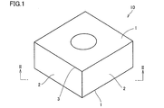
- a surface-coated cutting tool 10 (hereinafter simply referred to as “tool 10”) of the present embodiment has a cutting edge at which rake face 1, flank face 2, rake face 1 and flank face 2 intersect. And a ridge line portion 3. That is, the rake face 1 and the flank face 2 are faces that are connected with the blade edge line portion 3 interposed therebetween.
- the cutting edge ridge line portion 3 constitutes a cutting edge tip portion of the tool 10.
- the shape of such a tool 10 depends on the shape of the base material described later.
- FIG. 1 shows a tool 10 as a cutting edge exchangeable cutting tip for turning, but the tool 10 is not limited to this, and a drill, an end mill, a cutting edge exchangeable cutting tip for a drill, a cutting edge exchangeable cutting tip for an end mill, a milling cutter. It can be suitably used as a cutting tool such as a cutting edge exchangeable cutting tip for processing, a metal saw, a gear cutting tool, a reamer, and a tap.
- the tool 10 when the tool 10 is a cutting edge exchange type cutting tip or the like, the tool 10 includes those having a chip breaker and those having no chip breaker, and the cutting edge ridge line portion 3 has a sharp edge (rake face). (See Fig. 1), honing (with sharp edges added) (see Fig. 3), negative land (with chamfer), honing and negative land combined Any are included.
- the tool 10 includes a base material 11 and a coating 12 formed on the base material 11.
- the coating 12 preferably covers the entire surface of the substrate 11, but a part of the substrate 11 is not covered with the coating 12 or the configuration of the coating 12 is partially different. Even so, it does not depart from the scope of the present embodiment.
- the substrate 11 of the present embodiment has a rake face 11a, a flank face 11b, and a cutting edge ridge line portion 11c where the rake face 11a and the flank face 11b intersect.
- the rake face 11 a, the flank face 11 b, and the cutting edge ridge line part 11 c constitute a rake face 1, a flank face 2, and a cutting edge ridge line part 3 of the tool 10.
- any conventionally known substrate can be used as this type of substrate.
- cemented carbide for example, WC-based cemented carbide, including WC, including Co, or including carbonitrides such as Ti, Ta, Nb), cermet (TiC, TiN, TiCN, etc.) Component
- high-speed steel ceramics (titanium carbide, silicon carbide, silicon nitride, aluminum nitride, aluminum oxide, etc.), cubic boron nitride sintered body, or diamond sintered body preferable.
- the coating film 12 of this embodiment may include other layers as long as it includes the ⁇ -Al 2 O 3 layer.
- the other layer include a TiN layer, a TiCN layer, a TiBNO layer, a TiCNO layer, a TiB 2 layer, a TiAlN layer, a TiAlCN layer, a TiAlON layer, and a TiAlONC layer.
- the order of the lamination is not particularly limited.
- those having no particular atomic ratio in the chemical formulas such as “TiN”, “TiCN”, and “TiC x N y ” indicate that the atomic ratio of each element is only “1”. It is not shown and all conventionally known atomic ratios are included.
- Such a coating 12 of this embodiment has an action of improving various properties such as wear resistance and chipping resistance by covering the base material 11.
- the coating 12 has a thickness of 3 to 30 ⁇ m (3 ⁇ m or more and 30 ⁇ m or less.
- the range includes upper and lower numerical values), more preferably 5 to 20 ⁇ m. It is suitable to have. If the thickness is less than 3 ⁇ m, the wear resistance may be insufficient. If it exceeds 30 ⁇ m, peeling or breaking of the coating 12 occurs when a large stress is applied between the coating 12 and the substrate 11 in intermittent processing. May occur frequently.
- the film 12 of this embodiment includes an ⁇ -Al 2 O 3 layer.
- the ⁇ -Al 2 O 3 layer can be included in the coating film 12 in one layer or two or more layers.
- This ⁇ -Al 2 O 3 layer is a layer containing crystal grains of a plurality of ⁇ -Al 2 O 3 (aluminum oxide whose crystal structure is ⁇ -type). That is, this layer is composed of polycrystalline ⁇ -Al 2 O 3 . Usually, this crystal grain has a grain size of about 100 to 2000 nm. There is a “crystal grain boundary” between a plurality of ⁇ -Al 2 O 3 crystal grains.
- the crystal grain boundary has a great influence on material characteristics such as crystal grain growth, creep characteristics, diffusion characteristics, electrical characteristics, optical characteristics, and mechanical characteristics. Important properties to consider are, for example, grain boundary density in the material, chemical composition of the interface, and crystallographic structure, ie, grain interface orientation and grain orientation difference.
- CSL grain boundaries play a special role.
- a CSL grain boundary (also simply referred to as “CSL grain boundary”) is characterized by a multiplicity index ⁇ , which is the density of crystal lattice sites of two grains in contact with the grain boundary and both crystals. It is defined as the ratio with the density of the corresponding part when the lattices are overlapped.
- EBSD electron beam backscatter diffraction
- the crystallographic orientation is determined after indexing the corresponding diffraction pattern.
- structure analysis and determination of grain boundary character distribution are made relatively easily by using EBSD.
- EBSD grain boundary character distribution
- the misorientation distribution is associated with the processing conditions of the substance.
- Grain boundary orientation differences can be obtained by normal orientation parameters such as Euler angles, angle / axis pairs, or Rodrigues vectors.
- the CSL model is widely used as a characterization tool.
- the crystal grain boundaries in the ⁇ -Al 2 O 3 layer of the present embodiment include the above-described CSL grain boundaries and general grain boundaries.
- CSL grain boundaries are ⁇ 3 type grain boundary, ⁇ 7 type crystal grain boundary, ⁇ 11 type crystal grain boundary, ⁇ 17 type crystal grain boundary, ⁇ 19 type crystal grain boundary, ⁇ 21 type crystal grain boundary, ⁇ 23 type crystal grain boundary, and ⁇ 29 type Consists of grain boundaries.
- the general grain boundary is a grain boundary other than the CSL grain boundary. Therefore, the general grain boundary is a remaining portion obtained by removing the CSL grain boundary from the whole grain boundary of the ⁇ -Al 2 O 3 crystal grains when observed by EBSD.
- the ⁇ -Al 2 O 3 layer according to this embodiment satisfies the following (1) to (4).
- (1) shows ⁇ -Al 2 O 3 layer on the rake face side, and each of ⁇ -Al 2 O 3 layer of flank side (001) orientation;
- (2) In the alpha-Al 2 O 3 layer on the rake face side, the length of the ⁇ 3 type crystal grain boundary L R3 is 80% of the length of ⁇ 3-29 type crystal grain boundary L R3-29, and L R3-29 and general grain boundary length L RG total length of all the grain boundaries with the sum of the L R 10% or more is 50% or less;
- (3) In the ⁇ -Al 2 O 3 layer on the flank side, the length L F3 of the ⁇ 3-type grain boundary is more than 80% of the length L F3-29 of the ⁇ 3-29 type grain boundary, and 10% or more and 50% or less of the total length L F of all grain boundaries, which is the sum of L F3-29 and the length L FG of general grain boundaries;
- the ⁇ -Al 2 O 3 layer on each side indicates “(001) orientation” means that the normal direction to the (001) plane is the surface of the ⁇ -Al 2 O 3 layer (on the surface side of the coating).
- the ratio (area ratio) of crystal grains ( ⁇ -Al 2 O 3 ) that is within ⁇ 20 ° with respect to the normal direction of the surface to be positioned is 50% or more in the ⁇ -Al 2 O 3 layer. Say the case.
- the area to be color mapped in ⁇ -Al 2 O 3 layer, in the thickness direction are all in the range of ⁇ -Al 2 O 3 layer. That is, for all the regions of the surface located on the coated surface side of the ⁇ -Al 2 O 3 layer, to the surface located on the substrate side of the ⁇ -Al 2 O 3 layer, it is color mapped.
- the entire range in the thickness direction can be confirmed by one observation image.
- an arbitrary range may be color-mapped.
- alpha-Al 2 O about three layers of (001) orientation is increased, alpha-Al since the hardness of the 2 O 3 layer is increased, the (1) of the present embodiment to satisfy the alpha-Al 2 According to the O 3 layer, the generation of cracks due to impact during processing can be suppressed, and the toughness of the cutting tool can be greatly improved, so that high wear resistance can be achieved.
- surface side of the film in the thickness direction of the ⁇ -Al 2 O 3 layer, the substrate side means the opposite side, another layer ⁇ -Al 2 O 3 layer on is not formed In the case, it means the surface of the ⁇ -Al 2 O 3 layer.
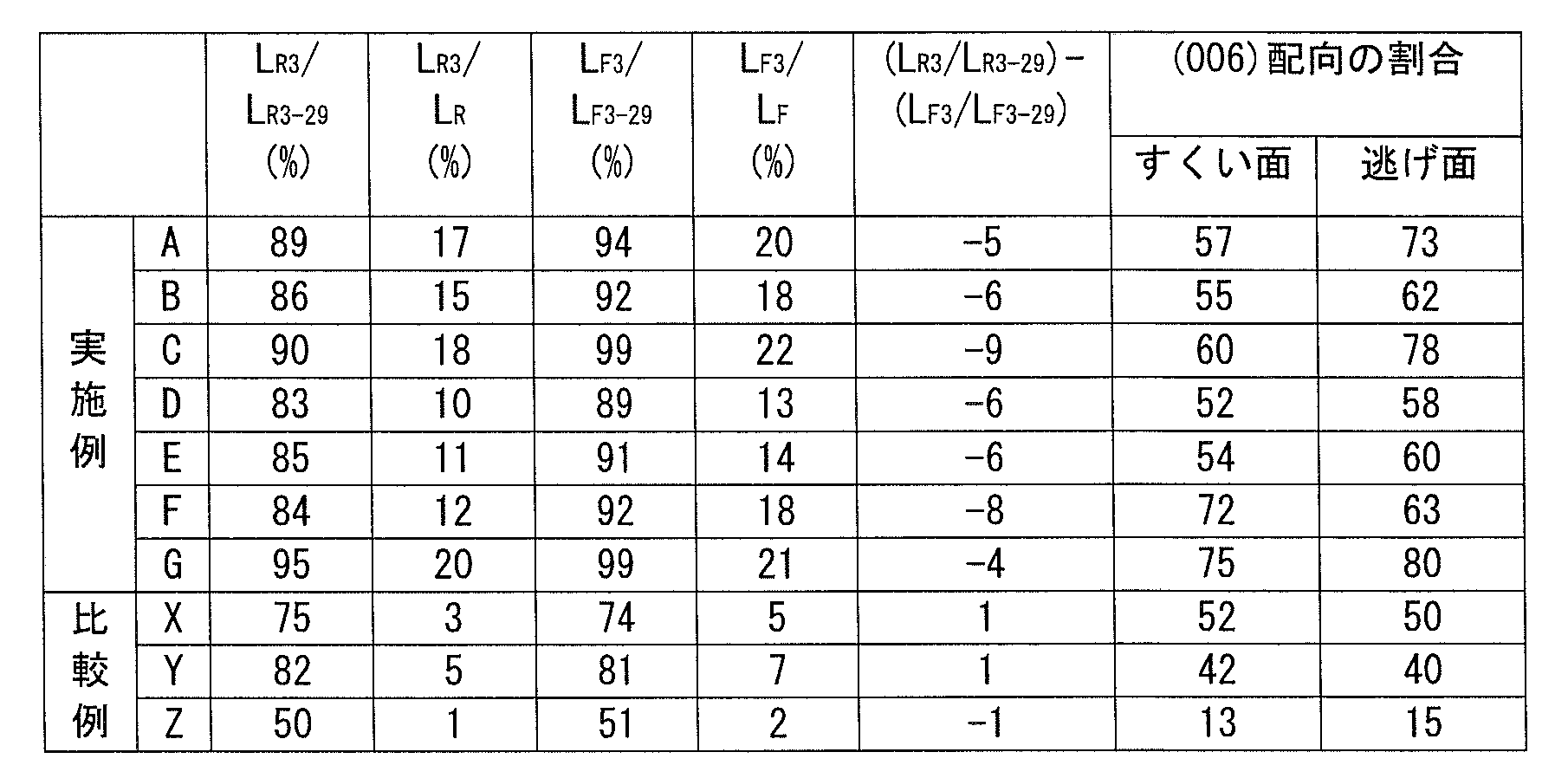
- the above (2) and (3) will be described.
- the ⁇ 3 type grain boundary is considered to have the lowest grain boundary energy among the CSL grain boundaries of ⁇ -Al 2 O 3. It is considered that the characteristics (particularly plastic deformation resistance) can be improved. Therefore, in the present embodiment, all CSL grain boundaries expressed by notation ⁇ 3-29 type grain boundaries of ⁇ 3 type crystal grain boundaries in ⁇ -Al 2 O 3 layer on the rake face side length L R3, defined as 80% of the length of ⁇ 3-29 type crystal grain boundaries in the rake face side ⁇ -Al 2 O 3 layer L R3-29, ⁇ 3 type crystal grains in the ⁇ -Al 2 O 3 layer of flank side field of length L F3, a definition of 80% of the length L R3-29 of ⁇ 3-29 type crystal grain boundaries in ⁇ -Al 2 O 3 layer of flank side.
- the length L R3 indicates the total length of the ⁇ 3-type grain boundaries in the field of view observed when the ⁇ -Al 2 O 3 layer on the rake face side is observed with an SEM equipped with EBSD.
- R3-29 when the ⁇ -Al 2 O 3 layer on the rake face side is observed using an SEM equipped with EBSD, ⁇ 3 type grain boundaries, ⁇ 7 type grain boundaries, ⁇ 11
- the total length of each of the type grain boundaries, ⁇ 17 type grain boundaries, ⁇ 19 type grain boundaries, ⁇ 21 type grain boundaries, ⁇ 23 type crystal grain boundaries, and ⁇ 29 type crystal grain boundaries is shown.
- the length L F3 indicates the total length of the ⁇ 3-type grain boundary in the field of view observed when the flank ⁇ -Al 2 O 3 layer is observed with an SEM equipped with EBSD.
- the length L F3-29 is the ⁇ 3 type grain boundary, ⁇ 7 type crystal in the field of view observed when the flank ⁇ -Al 2 O 3 layer is observed using a SEM equipped with EBSD.
- the total length of each of the grain boundaries, ⁇ 11 type grain boundaries, ⁇ 17 type crystal grain boundaries, ⁇ 19 type crystal grain boundaries, ⁇ 21 type crystal grain boundaries, ⁇ 23 type crystal grain boundaries, and ⁇ 29 type crystal grain boundaries is shown.
- the length L R3 is more preferably 83% or more of the length L R3-29 , and still more preferably 85% or more.
- the higher the value the better.
- this ⁇ 3 type grain boundary is a crystal grain boundary having high consistency as is clear from having a low grain boundary energy
- the ⁇ 3 type crystal grain boundary is 2
- One crystal grain behaves like a single crystal or twin crystal and tends to coarsen. When the crystal grains are coarsened, film characteristics such as chipping resistance are deteriorated, so that it is necessary to suppress the coarsening.
- the lengths L R and L F are defined as 10% or more and 50% or less of the lengths L R and L F , and ensure the above-described suppression effect.
- the length L R3 , L F3 of the ⁇ 3 type grain boundary exceeds 50% of the total length L R , L F of all the grain boundaries on each side, the crystal grains become coarse, which is not preferable. If it is less than%, the above-mentioned excellent mechanical properties cannot be obtained.
- a more preferable range of the lengths L R3 and L F3 of the ⁇ 3-type grain boundaries is 20 to 45%, and a more preferable range is 30 to 40%.
- the total grain boundary is a sum of general grain boundaries other than the CSL crystal grain boundaries and the CSL crystal grain boundaries. Accordingly, the “total length L R of all grain boundaries” on the rake face side can be expressed as “the sum of the length L R3-29 of the ⁇ 3-29 type grain boundary and the length L RG of the general grain boundary”. The “total length L F of all grain boundaries” on the flank side can be expressed as “the sum of ⁇ 3-29 type grain boundary length L F3-29 and general grain boundary length L FG ”. it can.
- the above (4) will be described.
- high-speed / low-feed cutting In cutting under high-speed conditions and low-feed conditions (hereinafter also referred to as “high-speed / low-feed cutting”), the heat load on the flank side is large, and wear on the flank surface tends to increase.
- the ⁇ -Al 2 O 3 layer satisfying the above (2) to (4) can withstand the load applied to the flank side, and therefore severe cutting conditions particularly on the flank side. Long life can be maintained even in high-speed and low-feed cutting.
- the difference ⁇ (L R3 / L R3-29 ) ⁇ (L F3 / L F3-29 ) ⁇ between the ratio L R3 / L R3-29 and the ratio L F3 / L F3-29 is ⁇ 1 to ⁇ 10. It is preferable. In this case, the balance between improvement of chipping resistance on the rake face side and improvement of plastic deformation resistance on the flank face side is excellent.
- the difference is more preferably ⁇ 4 to ⁇ 9.
- the length L R3 of the ⁇ 3-type grain boundary is preferably 80 to 95% of the length L R3-29 of the ⁇ 3-29 type grain boundary, and 83 to 95 %, More preferably 80 to 90%, and the length L F3 of the ⁇ 3-type grain boundary is 90 to 99% of the length L F3-29 of the ⁇ 3-29 type grain boundary. Preferably, it is 91 to 99%.
- an ⁇ -Al 2 O 3 layer is formed on a substrate based on a manufacturing method described later. Then, the formed ⁇ -Al 2 O 3 layer on the rake face side (including the base material) is cut so as to obtain a cross section perpendicular to the ⁇ -Al 2 O 3 layer (that is, ⁇ -Al 2 O cut surface obtained by cutting the alpha-Al 2 O 3 layer in the plane is cut to expose containing normal to the surface of the three layers). Thereafter, the cut surface is polished with water-resistant abrasive paper (containing a SiC abrasive abrasive as an abrasive).
- water-resistant abrasive paper containing a SiC abrasive abrasive as an abrasive.
- the above-mentioned cutting is performed, for example, on an ⁇ -Al 2 O 3 layer surface (if another layer is formed on the ⁇ -Al 2 O 3 layer, the coating surface) on a sufficiently large holding plate And fixed in close contact with wax or the like, and then cut in a direction perpendicular to the flat plate with a rotary blade cutter (cut so that the rotary blade and the flat plate are as vertical as possible) To do.
- This cutting can be performed at any part of the ⁇ -Al 2 O 3 layer as long as it is performed in such a vertical direction.
- the above polishing is performed using the water-resistant abrasive papers # 400, # 800, and # 1500 in order (the number (#) of the water-resistant abrasive paper means a difference in the particle size of the abrasive, and the number is The larger the particle size, the smaller the particle size of the abrasive).
- the polished surface is further smoothed by ion milling with Ar ions.
- the conditions for the ion milling treatment are as follows. Acceleration voltage: 6 kV
- the cutting position is set so as to avoid at least the vicinity of the edge portion 3 of the cutting edge.
- the outer edge A 1 of the region where the surface (shown by a dotted line extending in the left and right directions in FIG. 3) that contacts the rake surface 1 and the rake surface 1 contacts, and the surface that contacts the flank 2 A region connecting the outer edge A 2 of the region where the flank 2 is in contact with the flank 2 is regarded as the blade edge line portion 3, and at least from the outer edge A 1 that is the end of the blade edge line portion 3.
- 0.2mm or more away position position away from the outer edge a 1 to the left in FIG. 3
- SEM uses Zeiss Supra 35 VP (CARL ZEISS) equipped with HKL NL02 EBSD detector.
- EBSD data is collected sequentially by placing a focused electron beam onto each pixel individually.
- the normal of the sample surface (cross section of the smoothed ⁇ -Al 2 O 3 layer) is inclined by 70 ° with respect to the incident beam, and the analysis is performed at 15 kV. In order to avoid the charging effect, a pressure of 10 Pa is applied.
- the high current mode is used in combination with the opening diameter of 60 ⁇ m or 120 ⁇ m. Data collection is performed at a step of 0.1 ⁇ m / step for 500 ⁇ 300 points corresponding to a surface area of 50 ⁇ 30 ⁇ m on the polished surface.
- the normal direction of the (001) plane of each measurement pixel and the ⁇ -Al 2 O 3 layer surface (the coating surface side) is within ⁇ 20 °.
- the Tolerance 20 ° between the normal direction of the ⁇ -Al 2 O 3 layer surface and the normal direction of the (001) plane of each measurement pixel is 20 °.
- a color map (with a direction difference within ⁇ 20 °) is created. Then, by calculating the area ratio of the pixels based on this color map, when the area ratio is 50% or more, “the ⁇ -Al 2 O 3 layer on the rake face side exhibits (001) orientation”. Shall.
- the ⁇ -Al 2 O 3 layer on the flank side shows (001) orientation.
- Any ⁇ -Al 2 O 3 layer on the surface side exhibits (001) orientation, that is, the normal direction to the (001) surface is located on the surface of the ⁇ -Al 2 O 3 layer (the surface side of the coating).
- the ratio of crystal grains ( ⁇ -Al 2 O 3 ) within ⁇ 20 ° with respect to the normal direction of the surface) is 50% or more, the ⁇ -Al 2 O 3 layer is The above (1) is satisfied.
- each of the rake face side ⁇ -Al 2 O 3 layer and the flank face side ⁇ -Al 2 O 3 layer satisfies the above (2) and (3), and these are the above (4 ) Can be confirmed as follows.
- the normal of the sample surface (cross section of the smoothed ⁇ -Al 2 O 3 layer) is inclined by 70 ° with respect to the incident beam, and the analysis is performed at 15 kV. In order to avoid the charging effect, a pressure of 10 Pa is applied.
- the high current mode is used in combination with the opening diameter of 60 ⁇ m or 120 ⁇ m. Data collection is performed at a step of 0.1 ⁇ m / step for 500 ⁇ 300 points corresponding to a surface area of 50 ⁇ 30 ⁇ m on the polished surface.
- the ⁇ -Al 2 O 3 layer on the rake face side, the length of the ⁇ 3 type crystal grain boundary L R3, ⁇ 3-29 type crystal grain boundary length L R3-29, and the sum of Zentsubukai L R The length can be determined.
- the length of the ⁇ 3 type crystal grain boundaries in ⁇ -Al 2 O 3 layer of flank side L F3, ⁇ 3-29 type crystal grain boundary length L F3-29, and the sum of Zentsubukai L F The length can be determined.
- alpha-Al 2 O 3 layer on the rake face side can be alpha-Al 2 O 3 layer of flank side checks whether satisfies the above (2) and (3), further It can be confirmed whether the ⁇ -Al 2 O 3 layer satisfies the above (4).
- the ⁇ -Al 2 O 3 layer preferably has a thickness of 2 to 20 ⁇ m. Thereby, the above excellent effects can be exhibited.
- the thickness is more preferably 2 to 15 ⁇ m, and further preferably 2 to 10 ⁇ m.
- the thickness is less than 2 ⁇ m, the above-mentioned excellent effects may not be sufficiently exhibited.
- the thickness exceeds 20 ⁇ m, the linear expansion coefficient between the ⁇ -Al 2 O 3 layer and other layers such as the underlayer Interfacial stress due to the difference between the two may increase, and ⁇ -Al 2 O 3 crystal grains may fall off.
- SEM scanning electron microscope
- the ⁇ -Al 2 O 3 layer preferably has a surface roughness Ra of less than 0.2 ⁇ m.
- the surface roughness Ra is more preferably less than 0.15 ⁇ m, and even more preferably less than 0.10 ⁇ m.
- the lower the surface roughness Ra the better. It is not necessary to define the lower limit, but the lower limit is 0.05 ⁇ m or more from the viewpoint that the coating is affected by the surface properties of the substrate.
- surface roughness Ra shall mean arithmetic average roughness Ra of JISB0601 (2001).
- the ⁇ -Al 2 O 3 layer includes a point where the absolute value of the compressive stress is maximum in a region within 2 ⁇ m from the surface side of the coating, and the absolute value of the compressive stress at the point is preferably less than 1 GPa.
- the absolute value is more preferably less than 0.9 GPa, and still more preferably less than 0.8 GPa.
- the lower limit of the absolute value is not particularly limited, but the lower limit is 0.2 GPa or more from the viewpoint of a balance between wear resistance and fracture resistance.
- the compressive stress in this embodiment can be measured by the conventionally known sin 2 ⁇ method using X-rays, the penetration depth constant method, or the like.
- the coating of this embodiment can include a TiC x N y layer between the substrate and the ⁇ -Al 2 O 3 layer.
- This TiC x N y layer preferably contains TiC x N y that satisfies an atomic ratio of 0.6 ⁇ x / (x + y) ⁇ 0.8. This improves the adhesion between the substrate and the ⁇ -Al 2 O 3 layer.
- the atomic ratio is more preferably 0.65 ⁇ x / (x + y) ⁇ 0.75, and further preferably 0.67 ⁇ x / (x + y) ⁇ 0.72.
- x / (x + y) is less than 0.6, the wear resistance may be insufficient, and when it exceeds 0.8, the chipping resistance may be insufficient.
- the surface-coated cutting tool of this embodiment can be manufactured by forming a coating film on a substrate by a chemical vapor deposition (CVD) method.
- CVD chemical vapor deposition
- these layers can be formed under a conventionally known condition using a chemical vapor deposition apparatus.
- the ⁇ -Al 2 O 3 layer can be formed as follows.
- AlCl 3 , HCl, CO 2 , H 2 S, O 2 , and H 2 are used as source gases.
- the blending amounts are 3-5% by volume of AlCl 3 , 4-6% by volume of HCl, 0.5-2% by volume of CO 2 , 1-5% by volume of H 2 S, 0.0001-0 of O 2 .01% by volume, and the balance is H 2 .
- volume ratios of 0.1 ⁇ CO 2 / H 2 S ⁇ 1, 0.1 ⁇ CO 2 / AlCl 3 ⁇ 1, 0.5 ⁇ AlCl 3 / HCl ⁇ 1 are employed.
- the source gas is blown against the base material disposed in the reaction vessel of the chemical vapor deposition apparatus. At this time, the source gas is ejected in the direction of the base material flank with respect to the source gas ejection direction.
- the rake face of the substrate is adjusted so as to be substantially parallel to the jet direction of the source gas.
- the chemical vapor deposition conditions are as follows: the temperature is 950 to 1050 ° C., the pressure is 1 to 5 kPa, and the gas flow rate (total gas amount) is 50 to 100 L / min. Further, the introduction speed of the raw material gas into the reaction vessel is set to 1.7 to 3.5 m / sec.
- an ⁇ -Al 2 O 3 layer is once formed by chemical vapor deposition under the above conditions, and then annealed.
- the annealing conditions are a temperature of 1050 to 1080 ° C., a pressure of 50 to 100 kPa, and a time of 120 to 300 minutes.
- the annealing atmosphere is performed by flowing H 2 and Ar (argon) at a flow rate of 20 to 30 L / min.
- the ⁇ -Al 2 O 3 layer of the present embodiment having a desired thickness can be formed.
- the amount of O 2 in the source gas is within the above range
- the flank face of the base material is substantially perpendicular to the jet direction of the source gas
- the rake face of the base material is substantially parallel to the jet direction of the source gas.
- O 2 is more reactive than other gases such as CO 2 , and has the effect of increasing the number of ⁇ -Al 2 O 3 nuclei and increasing the film formation rate. O 2 can also have an action of reducing the proportion of the ⁇ 3-type grain boundaries in the CSL grain boundaries. This is because if the film formation rate is too high, it is difficult to generate a ⁇ 3 type crystal grain boundary that is a crystal grain boundary having high consistency.
- the flow velocity density of the source gas tends to be relatively high, and on the flank side that is substantially perpendicular to the jet direction of the source gas. Tends to have a relatively low flow velocity density of the source gas. That is, the residence time of the raw material gas tends to be shorter on the rake face side, and the residence time of the raw material gas tends to be longer on the flank face side.In other words, the rake face side is compared with the flank face side. The source gas tends to be supplied more frequently.
- a film was formed on the surface of each substrate obtained above.
- the base material was set in a chemical vapor deposition apparatus to form a film on the base material by chemical vapor deposition.
- the base material was disposed in the reaction vessel so that the rake face was substantially parallel to the gas ejection direction and the flank face was substantially orthogonal to the gas ejection direction.
- the film formation conditions are as described in Table 2 and Table 3 below.
- Table 2 shows the formation conditions of each layer other than the ⁇ -Al 2 O 3 layer
- Table 3 shows the formation conditions of the ⁇ -Al 2 O 3 layer.
- TiBNO and TiCNO in Table 2 are intermediate layers in Table 5 to be described later, and that other layers correspond to the layers other than the ⁇ -Al 2 O 3 layer in Table 5.
- TiC x N y layers are those atomic ratio x / (x + y) consists of TiC x N y is 0.7.
- the ⁇ -Al 2 O 3 layer has 10 formation conditions of A to G and X to Z, of which A to G are the conditions of the example, and X to Z are It is conditions of a comparative example (prior art).
- the introduction rate of the source gas was set to 2 m / sec, and the gas pipe for ejecting the source gas was rotated at 2 rpm while fixing the base material.
- the ⁇ -Al 2 O 3 layer of the example formed under the conditions of A to G was 1050 ° C., 50 kPa, H 2 flow rate was 20 L / min, Ar flow rate during the annealing time described in Table 3. Was annealed under the condition of 30 L / min.
- the formation condition A is 3.2 vol% AlCl 3 , 4.0 vol% HCl, 1.0 vol% CO 2 , 2 vol% H 2 S, 0.003 vol% O 2
- the raw material gas having the composition consisting of the balance H 2 is supplied to the chemical vapor deposition apparatus, and the chemical vapor deposition method is performed under the conditions of a pressure of 3.5 kPa and a temperature of 1000 ° C. and a flow rate (total gas amount) of 70 L / min. It is shown that an ⁇ -Al 2 O 3 layer is formed by performing annealing and then annealing for 180 minutes under the above conditions.
- each layer other than the ⁇ -Al 2 O 3 layer shown in Table 2 was similarly formed by chemical vapor deposition except that annealing was not performed. “Remaining” in Table 2 indicates that H 2 occupies the remainder of the source gas.
- the “total gas amount” indicates the total volume flow rate introduced into the chemical vapor deposition apparatus per unit time, assuming that the gas in the standard state (0 ° C., 1 atm) is an ideal gas ( ⁇ in Table 3). The same applies to the Al 2 O 3 layer).
- the thickness of each layer was adjusted by appropriately adjusting the film formation time (the film formation speed of each layer is about 0.5 to 2.0 ⁇ m / hour).
- each coating was confirmed by SEM-EDX (scanning electron microscope-energy dispersive X-ray spectroscopy), and the length of the ⁇ 3-type grain boundary of the ⁇ -Al 2 O 3 layer was confirmed.
- the length of the ⁇ 3-29 type grain boundary and the total length of all the grain boundaries were confirmed by the method described above.
- the normal direction with respect to the (001) plane is changed to the ⁇ -Al 2 O 3 layer surface (the surface located on the coating surface side) and The ratio (%) of crystal grains ( ⁇ -Al 2 O 3 ) within ⁇ 20 ° with respect to the normal direction of
- the surface-coated cutting tool of Example 1 employs the base material P described in Table 1 as a base material, and a TiN layer having a thickness of 1.2 ⁇ m as a base layer on the surface of the base material P.
- a TiC x N y layer having a thickness of 13.0 ⁇ m is formed on the underlayer under the conditions shown in Table 2
- a TiBNO layer having a thickness of 0.7 ⁇ m is formed on the TiC x N y layer as an intermediate layer.
- an ⁇ -Al 2 O 3 layer having a thickness of 8.6 ⁇ m was formed on the intermediate layer under the conditions shown in Table 3.
- a TiN layer having a thickness of 0.9 ⁇ m was formed as the outermost layer.
- the film having a total thickness of 24.3 ⁇ m is formed on the substrate.
- a blank in Table 4 indicates that the corresponding layer is not formed.
- the length of the ⁇ 3 type crystal grain boundary L R3, the length of ⁇ 3-29 type crystal grain boundary L R3 -29 is 89%, and 17% of the total length L R of Zentsubukai.
- the length L F3 of the ⁇ 3-type grain boundary is 94% of the length L F3-29 of the ⁇ 3-29 type grain boundary, and all the grain boundaries total 20% of the length L F.
- ⁇ Cutting test> The following two types of cutting tests were performed using the surface-coated cutting tool obtained above. The following cutting tests are similar to high-speed, low-feed cutting.
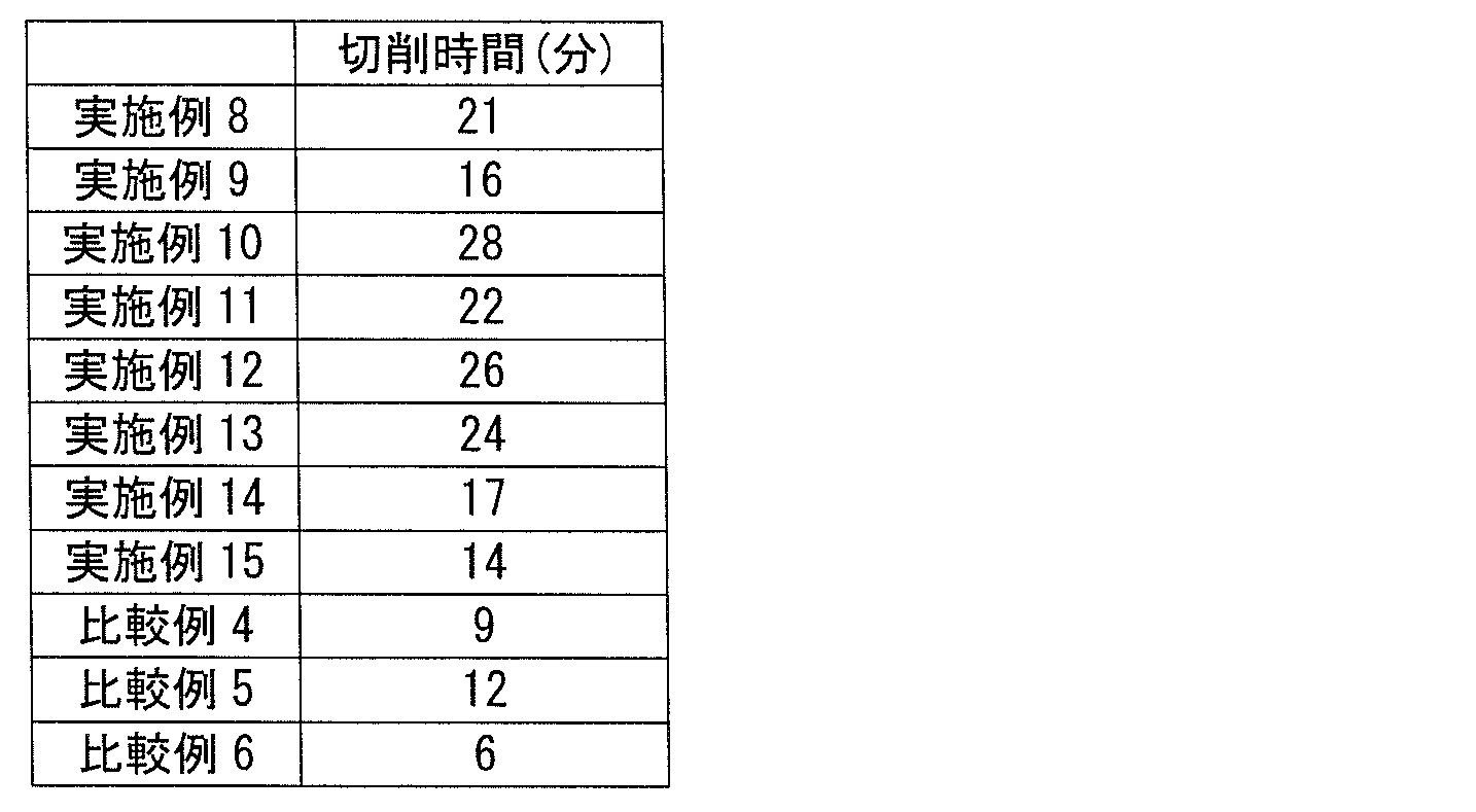
- the surface-coated cutting tool of the example is superior in both wear resistance and chipping resistance to the surface-coated cutting tool of the comparative example, and the tool life is prolonged. It is obvious. That is, it was confirmed that the mechanical properties of the coating of the surface-coated cutting tool of the example were improved.
- the surface-coated cutting tool of the example is superior to the surface-coated cutting tool of the comparative example in fracture resistance and it is clear that the tool life is prolonged. That is, it was confirmed that the mechanical properties of the coating of the surface-coated cutting tool of the example were improved.
- Example 1A the surface-coated cutting tools of Example 1A, Example 2A, and Example 11A were obtained by subjecting the ⁇ -Al 2 O 3 layer of each surface-coated cutting tool to an aero lapping process under the following conditions, respectively. Was made. Then, for each of these surface-coated cutting tools, the surface roughness Ra of the ⁇ -Al 2 O 3 layer was measured in the same manner as described above. The results are shown in Table 10.
- ⁇ Aero wrap conditions> Media: Elastic rubber media with a diameter of about 1 mm containing diamond abrasive grains with an average particle size of 0.1 ⁇ m (trade name: “Multicon”, manufactured by Yamashita Towers) Projection pressure: 0.5 bar Projection time: 30 seconds wet / dry: dry.
- the surface-coated cutting tools of Examples 1A, 2A, and 11A having the ⁇ -Al 2 O 3 layer having the surface roughness Ra of less than 0.2 ⁇ m have a surface roughness of 0.2 ⁇ m or more.
- the coefficient of friction between the chip and the tool edge is reduced, and stable chip discharge is achieved. It was confirmed that it was possible to demonstrate the properties.
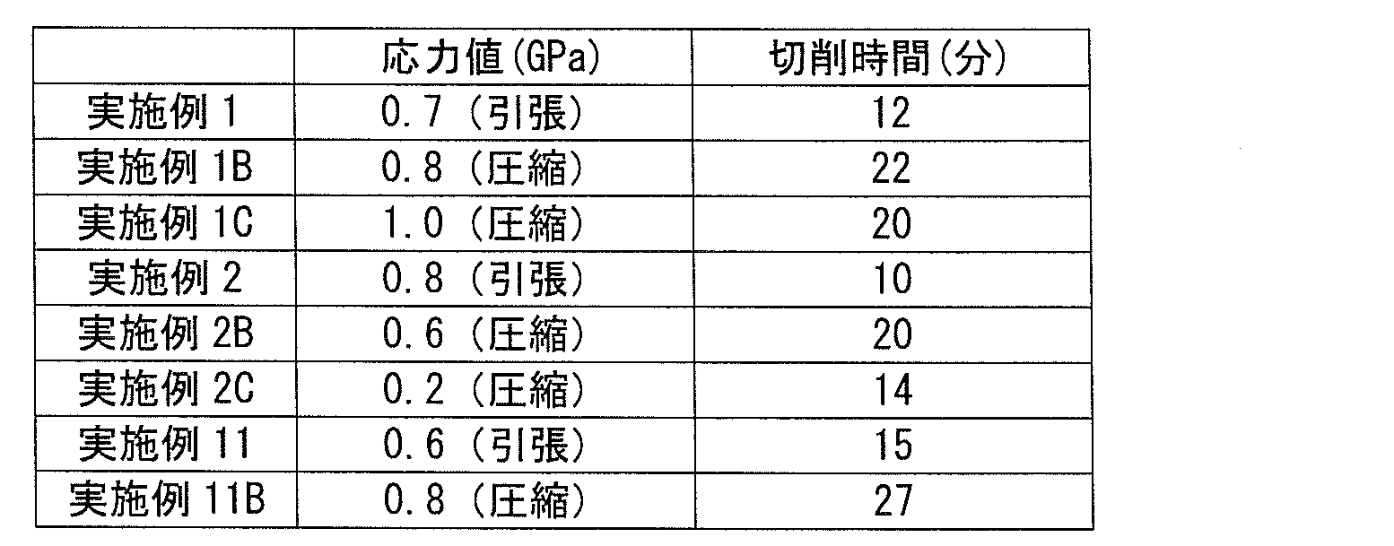
- Example 1B, Example 1C, Example 2B, Example 2C, and A surface-coated cutting tool of Example 11B was produced.
- Example 1B, Example 1C, Example 2B, Example 2C, and A surface-coated cutting tool of Example 11B was produced.
- Example 1B, Example 1C, Example 2B, Example 2C, and A surface-coated cutting tool of Example 11B was produced.
- Example 1B, Example 1C, Example 2B, Example 2C, and A surface-coated cutting tool of Example 11B was produced for each of these surface-coated cutting tools.
- the ⁇ -Al 2 O 3 layer includes a point where the absolute value of the stress is maximum in a region within 2 ⁇ m from the surface side of the coating, and the stress at that point is a tensile stress.
- the absolute value of the compressive stress is less than 1 GPa, chipping of the tool edge due to mechanical and thermal fatigue that occurs during intermittent cutting is suppressed, and as a result, the reliability of the edge is improved. Was confirmed.
Landscapes
- Chemical & Material Sciences (AREA)
- Engineering & Computer Science (AREA)
- Mechanical Engineering (AREA)
- Metallurgy (AREA)
- Organic Chemistry (AREA)
- Chemical Kinetics & Catalysis (AREA)
- Materials Engineering (AREA)
- Inorganic Chemistry (AREA)
- General Chemical & Material Sciences (AREA)
- Ceramic Engineering (AREA)
- Cutting Tools, Boring Holders, And Turrets (AREA)
- Chemical Vapour Deposition (AREA)
- Drilling Tools (AREA)
- Milling, Broaching, Filing, Reaming, And Others (AREA)
- Gear Processing (AREA)
Abstract
Description
最初に本開示の実施態様を列記して説明する。
以下、本発明の実施形態(以下「本実施形態」とも記す)に係る表面被覆切削工具について、図1~図3を用いながら、さらに詳細に説明する。
図1を参照し、本実施形態の表面被覆切削工具10(以下、単に「工具10」と記す)は、すくい面1と、逃げ面2と、すくい面1と逃げ面2とが交差する刃先稜線部3とを有する。すなわち、すくい面1と逃げ面2とは、刃先稜線部3を挟んで繋がる面である。刃先稜線部3は、工具10の切刃先端部を構成する。このような工具10の形状は、後述する基材の形状に依拠する。
本実施形態の基材11は、すくい面11aと、逃げ面11bと、すくい面11aと逃げ面11bとが交差する刃先稜線部11cとを有する。すくい面11a、逃げ面11b、および刃先稜線部11cは、工具10のすくい面1、逃げ面2、および刃先稜線部3を構成する。
本実施形態の被膜12は、α-Al2O3層を含む限り、他の層を含んでいてもよい。他の層としては、たとえばTiN層、TiCN層、TiBNO層、TiCNO層、TiB2層、TiAlN層、TiAlCN層、TiAlON層、TiAlONC層等を挙げることができる。その積層の順も特に限定されない。
本実施形態の被膜12は、α-Al2O3層を含む。このα-Al2O3層は、当該被膜12中に一層または二層以上含まれることができる。
(1)すくい面側のα-Al2O3層、および逃げ面側のα-Al2O3層は各々(001)配向を示す;
(2)すくい面側のα-Al2O3層において、Σ3型結晶粒界の長さLR3は、Σ3-29型結晶粒界の長さLR3-29の80%超であり、かつLR3-29と一般粒界の長さLRGとの和である全粒界の合計長さLRの10%以上50%以下である;
(3)逃げ面側のα-Al2O3層において、Σ3型結晶粒界の長さLF3は、Σ3-29型結晶粒界の長さLF3-29の80%超であり、かつLF3-29と一般粒界の長さLFGとの和である全粒界の合計長さLFの10%以上50%以下である;
(4)長さLR3と長さLR3-29との比LR3/LR3-29は、長さLF3と長さLF3-29との比LF3/LF3-29よりも小さい。
加速電圧:6kV
照射角度:α-Al2O3層表面の法線方向(すなわち該切断面におけるα-Al2O3層の厚み方向に平行となる直線方向)から0°
照射時間:6時間。
α-Al2O3層は、2~20μmの厚みを有することが好ましい。これにより、上記のような優れた効果を発揮することができる。その厚みは、2~15μmであることがより好ましく、2~10μmであることがさらに好ましい。
α-Al2O3層は、表面粗さRaが0.2μm未満であることが好ましい。これにより、切りくずと工具刃先との間の摩擦係数が低減し、耐チッピング性が向上するだけでなく、安定した切りくず排出性を発揮できる。表面粗さRaは、0.15μm未満であることがより好ましく、0.10μm未満であることがさらに好ましい。このように表面粗さRaは、低くなればなる程好ましく、その下限を規定する必要はないが、被膜は基材の表面性状の影響を受けるという観点からその下限は0.05μm以上である。
α-Al2O3層は、被膜の表面側から2μm以内の領域に圧縮応力の絶対値が最大となる地点を含み、該地点における圧縮応力の絶対値は1GPa未満であることが好ましい。これにより、断続切削加工時に発生する工具刃先の機械的、熱的疲労に伴う刃先の突発欠損が抑制され、省人/省エネルギー効果を発揮できる。該絶対値は、より好ましくは0.9GPa未満であり、さらに好ましくは0.8GPa未満である。上記絶対値の下限は、特に限定されないが、耐摩耗性と耐欠損性のバランスという観点からその下限は0.2GPa以上である。
本実施形態の被膜は、基材とα-Al2O3層との間にTiCxNy層を含むことができる。このTiCxNy層は、0.6≦x/(x+y)≦0.8という関係の原子比を満たすTiCxNyを含むことが好ましい。これにより、基材とα-Al2O3層との密着性が向上する。
本実施形態の表面被覆切削工具は、基材上に被膜を化学気相蒸着(CVD)法により形成することによって製造することができる。被膜のうち、α-Al2O3層以外の層が形成される場合、それらの層は化学気相蒸着装置を用いて従来公知の条件で形成することができる。一方、α-Al2O3層は、以下のようにして形成することができる。
以下の表1に記載の基材Pおよび基材Kの2種類の基材を準備した。具体的には、表1に記載の配合組成からなる原料粉末を均一に混合し、所定の形状に加圧成形した後、1300~1500℃で1~2時間焼結することにより、形状がCNMG120408NUX(住友電気工業製)の超硬合金製の基材を得た。

上記で得られた各基材に対してその表面に被膜を形成した。具体的には、基材を化学気相蒸着装置内にセットすることにより、基材上に化学気相蒸着法により被膜を形成した。基材は、すくい面がガスの噴出方向に略平行となり、逃げ面がガスの噴出方向に略直交となるように反応容器内に配置した。


上記の表2および表3の条件により基材上に被膜を形成することにより、以下の表4および表5に示した実施例1~15および比較例1~6の表面被覆切削工具を作製した。
上記で得られた表面被覆切削工具を用いて、以下の2種類の切削試験を行なった。以下の切削試験は、高速・低送り切削加工に類する。
以下の表6に記載した実施例および比較例の表面被覆切削工具について、以下の切削条件により逃げ面摩耗量(Vb)が0.20mmとなるまでの切削時間を測定するとともに刃先の最終損傷形態を観察した。その結果を表6に示す。切削時間が長いもの程、耐摩耗性に優れ、工具寿命が長くなっていることを示す。
被削材:SCM435丸棒外周切削
周速:400m/min
送り速度:0.1mm/rev
切込み量:1.0mm
切削液:あり。

以下の表7に記載した実施例および比較例の表面被覆切削工具について、以下の切削条件によりクレーター摩耗量(Kt)が0.20mmとなるまでの切削時間を測定した。その結果を表7に示す。切削時間が長いもの程、耐摩耗性に優れ、工具寿命が長くなっていることを示す。
被削材:S55C丸棒外周切削
周速:300m/min
送り速度:0.05mm/rev
切込み量:2.0mm
切削液:あり。
実施例1、実施例2、および実施例11の表面被覆切削工具に対して、α-Al2O3層の表面粗さRaをJIS B 0601(2001)に従って測定した。その結果を表10に示す。
メディア:平均粒径0.1μmのダイヤモンド砥粒を含んだ直径1mm程度の弾性ゴムメディア(商品名:「マルチコン」、ヤマシタワークス社製)
投射圧力:0.5bar
投射時間:30秒
湿式/乾式:乾式。
被削材:SS400丸棒外周切削
周速:300m/min
送り速度:0.1mm/rev
切込み量:1.0mm
切削液:なし。

実施例1、実施例2、および実施例11の表面被覆切削工具に対して、α-Al2O3層において被膜の表面側から2μm以内の領域に応力の絶対値が最大となる地点があることを確認し、その地点における応力の絶対値を測定した。その結果を表11(「応力値」の項)に示す。なお、応力の測定はX線を用いたsin2ψ法により実行し、表11の「応力値」の項において、数値は絶対値を示し、引張応力は「引張」、圧縮応力は「圧縮」と表記した。
メディア:アルミナメディア(φ50μm)
投射圧力:1~2bar
投射時間:10秒
湿式/乾式:湿式。
被削材:SUS304(60°×3溝外周切削)
周速:250m/min
送り速度:0.05mm/rev
切込み量:1.0mm
切削液:なし。
Claims (6)
- すくい面および逃げ面を有する表面被覆切削工具であって、
基材と、前記基材上に形成された被膜とを備え、
前記被膜は、α-Al2O3層を含み、
前記α-Al2O3層は、複数のα-Al2O3の結晶粒を含み、
前記結晶粒の粒界は、CSL粒界と、一般粒界とを含み、
すくい面側のα-Al2O3層は(001)配向を示し、
前記すくい面側のα-Al2O3層において、CSL粒界のうちΣ3型結晶粒界の長さLR3は、Σ3-29型結晶粒界の長さLR3-29の80%超であり、かつ前記長さLR3-29と一般粒界LRGの長さとの和である全粒界の合計長さLRの10%以上50%以下であり、
逃げ面側のα-Al2O3層は(001)配向を示し、
前記逃げ面側のα-Al2O3層において、CSL粒界のうちΣ3型結晶粒界の長さLF3は、Σ3-29型結晶粒界の長さLF3-29の80%超であり、かつ前記長さLF3-29と一般粒界の長さLFGとの和である全粒界の合計長さLFの10%以上50%以下であり、
前記長さLR3と前記長さLR3-29との比LR3/LR3-29は、前記長さLF3と前記長さLF3-29との比LF3/LF3-29よりも小さい、表面被覆切削工具。 - 前記CSL粒界は、Σ3型結晶粒界、Σ7型結晶粒界、Σ11型結晶粒界、Σ17型結晶粒界、Σ19型結晶粒界、Σ21型結晶粒界、Σ23型結晶粒界、およびΣ29型結晶粒界からなり、
前記長さLR3-29は、前記すくい面側のα-Al2O3層におけるΣ3型結晶粒界、Σ7型結晶粒界、Σ11型結晶粒界、Σ17型結晶粒界、Σ19型結晶粒界、Σ21型結晶粒界、Σ23型結晶粒界、およびΣ29型結晶粒界のそれぞれの長さの総計であり、
前記長さLF3-29は、前記逃げ面側のα-Al2O3層におけるΣ3型結晶粒界、Σ7型結晶粒界、Σ11型結晶粒界、Σ17型結晶粒界、Σ19型結晶粒界、Σ21型結晶粒界、Σ23型結晶粒界、およびΣ29型結晶粒界のそれぞれの長さの総計である、請求項1に記載の表面被覆切削工具。 - 前記α-Al2O3層は、2~20μmの厚みを有する、請求項1または請求項2に記載の表面被覆切削工具。
- 前記α-Al2O3層は、表面粗さRaが0.2μm未満である、請求項1から請求項3のいずれか1項に記載の表面被覆切削工具。
- 前記α-Al2O3層は、前記被膜の表面側から2μm以内の領域に圧縮応力の絶対値が最大となる地点を含み、前記地点における圧縮応力の絶対値は1GPa未満である、請求項1から請求項4のいずれか1項に記載の表面被覆切削工具。
- 前記被膜は、前記基材と前記α-Al2O3層との間にTiCxNy層を含み、
前記TiCxNy層は、0.6≦x/(x+y)≦0.8という関係の原子比を満たすTiCxNyを含む、請求項1から請求項5のいずれか1項に記載の表面被覆切削工具。
Priority Applications (6)
| Application Number | Priority Date | Filing Date | Title |
|---|---|---|---|
| US15/100,008 US9878373B2 (en) | 2015-07-13 | 2015-07-13 | Surface-coated cutting tool |
| EP15882291.6A EP3323539B1 (en) | 2015-07-13 | 2015-07-13 | Surface-coated cutting tool |
| JP2015548515A JP5871354B1 (ja) | 2015-07-13 | 2015-07-13 | 表面被覆切削工具 |
| KR1020167016205A KR102126103B1 (ko) | 2015-07-13 | 2015-07-13 | 표면 피복 절삭 공구 |
| CN201580003729.7A CN106536100B (zh) | 2015-07-13 | 2015-07-13 | 表面被覆切削工具 |
| PCT/JP2015/070030 WO2017009929A1 (ja) | 2015-07-13 | 2015-07-13 | 表面被覆切削工具 |
Applications Claiming Priority (1)
| Application Number | Priority Date | Filing Date | Title |
|---|---|---|---|
| PCT/JP2015/070030 WO2017009929A1 (ja) | 2015-07-13 | 2015-07-13 | 表面被覆切削工具 |
Publications (1)
| Publication Number | Publication Date |
|---|---|
| WO2017009929A1 true WO2017009929A1 (ja) | 2017-01-19 |
Family
ID=55362138
Family Applications (1)
| Application Number | Title | Priority Date | Filing Date |
|---|---|---|---|
| PCT/JP2015/070030 WO2017009929A1 (ja) | 2015-07-13 | 2015-07-13 | 表面被覆切削工具 |
Country Status (6)
| Country | Link |
|---|---|
| US (1) | US9878373B2 (ja) |
| EP (1) | EP3323539B1 (ja) |
| JP (1) | JP5871354B1 (ja) |
| KR (1) | KR102126103B1 (ja) |
| CN (1) | CN106536100B (ja) |
| WO (1) | WO2017009929A1 (ja) |
Families Citing this family (6)
| Publication number | Priority date | Publication date | Assignee | Title |
|---|---|---|---|---|
| WO2015146507A1 (ja) * | 2014-03-25 | 2015-10-01 | 兼房株式会社 | 切削工具 |
| US11286570B2 (en) * | 2017-01-26 | 2022-03-29 | Walter Ag | Coated cutting tool |
| KR102495052B1 (ko) * | 2018-10-15 | 2023-02-06 | 스미또모 덴꼬오 하드메탈 가부시끼가이샤 | 절삭 공구 |
| JP7167966B2 (ja) * | 2020-07-08 | 2022-11-09 | 株式会社タンガロイ | 被覆切削工具 |
| JP7167965B2 (ja) * | 2020-07-08 | 2022-11-09 | 株式会社タンガロイ | 被覆切削工具 |
| JP7302617B2 (ja) * | 2021-02-26 | 2023-07-04 | 株式会社タンガロイ | 被覆切削工具 |
Citations (6)
| Publication number | Priority date | Publication date | Assignee | Title |
|---|---|---|---|---|
| JP2006198735A (ja) | 2005-01-21 | 2006-08-03 | Mitsubishi Materials Corp | 硬質被覆層が高速断続切削加工ですぐれた耐チッピング性を発揮する表面被覆サーメット製切削工具 |
| JP2006326713A (ja) * | 2005-05-24 | 2006-12-07 | Mitsubishi Materials Corp | 厚膜化α型酸化アルミニウム層がすぐれた耐チッピング性を発揮する表面被覆サーメット製切削工具 |
| WO2010106811A1 (ja) * | 2009-03-18 | 2010-09-23 | 三菱マテリアル株式会社 | 表面被覆切削工具 |
| JP2014018886A (ja) * | 2012-07-13 | 2014-02-03 | Mitsubishi Materials Corp | 硬質被覆層がすぐれた初期なじみ性、耐チッピング性を発揮する表面被覆切削工具 |
| WO2014132995A1 (ja) * | 2013-02-26 | 2014-09-04 | 三菱マテリアル株式会社 | 表面被覆切削工具 |
| JP2014526391A (ja) | 2011-09-16 | 2014-10-06 | バルター アクチェンゲゼルシャフト | 結晶粒界を操作したアルファ‐アルミナでコーティングされた切削工具 |
Family Cites Families (11)
| Publication number | Priority date | Publication date | Assignee | Title |
|---|---|---|---|---|
| JPS5642412A (en) * | 1979-09-14 | 1981-04-20 | Yokogawa Hokushin Electric Corp | Automatic gain control circuit |
| JP2004122264A (ja) | 2002-09-30 | 2004-04-22 | Sumitomo Electric Ind Ltd | 被覆切削工具 |
| EP1788124B1 (en) * | 2005-11-18 | 2008-09-24 | Mitsubishi Materials Corporation | Surface coated cutting tool made of cermet having property-modified alpha type Al2O3 layer of hard coating layer |
| JP2007136631A (ja) * | 2005-11-21 | 2007-06-07 | Sumitomo Electric Hardmetal Corp | 刃先交換型切削チップ |
| EP2085500B1 (en) * | 2007-12-28 | 2013-02-13 | Mitsubishi Materials Corporation | Surface-coated cutting tool with hard coating layer having excellent abrasion resistance |
| WO2009133814A1 (ja) | 2008-04-30 | 2009-11-05 | 住友電気工業株式会社 | 表面被覆切削工具 |
| JP5440311B2 (ja) * | 2010-03-25 | 2014-03-12 | 三菱マテリアル株式会社 | 硬質被覆層がすぐれた耐剥離性と耐摩耗性を発揮する表面被覆切削工具 |
| JP5831707B2 (ja) * | 2012-03-14 | 2015-12-09 | 三菱マテリアル株式会社 | 硬質被覆層が高速断続切削ですぐれた耐チッピング性を発揮する表面被覆切削工具 |
| KR20140001694A (ko) * | 2012-06-28 | 2014-01-07 | 대구텍 유한회사 | 절삭 인서트 |
| JP6150109B2 (ja) * | 2013-04-18 | 2017-06-21 | 三菱マテリアル株式会社 | 硬質被覆層がすぐれた耐チッピング性を発揮する表面被覆切削工具 |
| JP6233575B2 (ja) * | 2013-11-22 | 2017-11-22 | 三菱マテリアル株式会社 | 高速断続切削加工で硬質被覆層がすぐれた耐チッピング性を発揮する表面被覆切削工具 |
-
2015
- 2015-07-13 KR KR1020167016205A patent/KR102126103B1/ko active IP Right Grant
- 2015-07-13 JP JP2015548515A patent/JP5871354B1/ja active Active
- 2015-07-13 CN CN201580003729.7A patent/CN106536100B/zh active Active
- 2015-07-13 WO PCT/JP2015/070030 patent/WO2017009929A1/ja active Application Filing
- 2015-07-13 EP EP15882291.6A patent/EP3323539B1/en active Active
- 2015-07-13 US US15/100,008 patent/US9878373B2/en active Active
Patent Citations (6)
| Publication number | Priority date | Publication date | Assignee | Title |
|---|---|---|---|---|
| JP2006198735A (ja) | 2005-01-21 | 2006-08-03 | Mitsubishi Materials Corp | 硬質被覆層が高速断続切削加工ですぐれた耐チッピング性を発揮する表面被覆サーメット製切削工具 |
| JP2006326713A (ja) * | 2005-05-24 | 2006-12-07 | Mitsubishi Materials Corp | 厚膜化α型酸化アルミニウム層がすぐれた耐チッピング性を発揮する表面被覆サーメット製切削工具 |
| WO2010106811A1 (ja) * | 2009-03-18 | 2010-09-23 | 三菱マテリアル株式会社 | 表面被覆切削工具 |
| JP2014526391A (ja) | 2011-09-16 | 2014-10-06 | バルター アクチェンゲゼルシャフト | 結晶粒界を操作したアルファ‐アルミナでコーティングされた切削工具 |
| JP2014018886A (ja) * | 2012-07-13 | 2014-02-03 | Mitsubishi Materials Corp | 硬質被覆層がすぐれた初期なじみ性、耐チッピング性を発揮する表面被覆切削工具 |
| WO2014132995A1 (ja) * | 2013-02-26 | 2014-09-04 | 三菱マテリアル株式会社 | 表面被覆切削工具 |
Non-Patent Citations (2)
| Title |
|---|
| D, BRANDON, ACTA METALL., vol. 14, 1966, pages 1479 - 1484 |
| H. GRIMMER; R. BONNET, PHILOSOPHICAL MAGAZINE A, vol. 61, 1990, pages 493 - 509 |
Also Published As
| Publication number | Publication date |
|---|---|
| JPWO2017009929A1 (ja) | 2017-07-13 |
| US9878373B2 (en) | 2018-01-30 |
| KR102126103B1 (ko) | 2020-06-23 |
| KR20180025779A (ko) | 2018-03-09 |
| CN106536100B (zh) | 2019-06-14 |
| CN106536100A (zh) | 2017-03-22 |
| EP3323539B1 (en) | 2019-03-20 |
| EP3323539A4 (en) | 2018-06-27 |
| EP3323539A1 (en) | 2018-05-23 |
| JP5871354B1 (ja) | 2016-03-01 |
| US20170189967A1 (en) | 2017-07-06 |
Similar Documents
| Publication | Publication Date | Title |
|---|---|---|
| JP5872747B1 (ja) | 表面被覆切削工具 | |
| JP5871354B1 (ja) | 表面被覆切削工具 | |
| JP5872748B1 (ja) | 表面被覆切削工具 | |
| JP6507457B2 (ja) | 表面被覆切削工具の製造方法 | |
| JP5884004B1 (ja) | 表面被覆切削工具 | |
| JP5871353B1 (ja) | 表面被覆切削工具 | |
| JP6507456B2 (ja) | 表面被覆切削工具の製造方法 | |
| JP6439200B2 (ja) | 表面被覆切削工具の製造方法 | |
| JP5871355B1 (ja) | 表面被覆切削工具 | |
| JP6550661B2 (ja) | 表面被覆切削工具の製造方法 | |
| JP6535922B2 (ja) | 表面被覆切削工具の製造方法 | |
| JP6439201B2 (ja) | 表面被覆切削工具の製造方法 |
Legal Events
| Date | Code | Title | Description |
|---|---|---|---|
| ENP | Entry into the national phase |
Ref document number: 2015548515 Country of ref document: JP Kind code of ref document: A |
|
| WWE | Wipo information: entry into national phase |
Ref document number: 15100008 Country of ref document: US |
|
| ENP | Entry into the national phase |
Ref document number: 20167016205 Country of ref document: KR Kind code of ref document: A |
|
| 121 | Ep: the epo has been informed by wipo that ep was designated in this application |
Ref document number: 15882291 Country of ref document: EP Kind code of ref document: A1 |
|
| NENP | Non-entry into the national phase |
Ref country code: DE |
|
| WWE | Wipo information: entry into national phase |
Ref document number: 2015882291 Country of ref document: EP |