US8395925B2 - Forming method for variable resistance nonvolatile memory element, and variable resistance nonvolatile memory device - Google Patents
Forming method for variable resistance nonvolatile memory element, and variable resistance nonvolatile memory device Download PDFInfo
- Publication number
- US8395925B2 US8395925B2 US13/001,943 US201013001943A US8395925B2 US 8395925 B2 US8395925 B2 US 8395925B2 US 201013001943 A US201013001943 A US 201013001943A US 8395925 B2 US8395925 B2 US 8395925B2
- Authority
- US
- United States
- Prior art keywords
- voltage
- forming
- variable resistance
- nonvolatile memory
- pulse
- Prior art date
- Legal status (The legal status is an assumption and is not a legal conclusion. Google has not performed a legal analysis and makes no representation as to the accuracy of the status listed.)
- Active, expires
Links
Images


Classifications
-
- G—PHYSICS
- G11—INFORMATION STORAGE
- G11C—STATIC STORES
- G11C13/00—Digital stores characterised by the use of storage elements not covered by groups G11C11/00, G11C23/00, or G11C25/00
- G11C13/0002—Digital stores characterised by the use of storage elements not covered by groups G11C11/00, G11C23/00, or G11C25/00 using resistive RAM [RRAM] elements
- G11C13/0021—Auxiliary circuits
- G11C13/0069—Writing or programming circuits or methods
-
- G—PHYSICS
- G11—INFORMATION STORAGE
- G11C—STATIC STORES
- G11C13/00—Digital stores characterised by the use of storage elements not covered by groups G11C11/00, G11C23/00, or G11C25/00
- G11C13/0002—Digital stores characterised by the use of storage elements not covered by groups G11C11/00, G11C23/00, or G11C25/00 using resistive RAM [RRAM] elements
- G11C13/0007—Digital stores characterised by the use of storage elements not covered by groups G11C11/00, G11C23/00, or G11C25/00 using resistive RAM [RRAM] elements comprising metal oxide memory material, e.g. perovskites
-
- G—PHYSICS
- G11—INFORMATION STORAGE
- G11C—STATIC STORES
- G11C13/00—Digital stores characterised by the use of storage elements not covered by groups G11C11/00, G11C23/00, or G11C25/00
- G11C13/0002—Digital stores characterised by the use of storage elements not covered by groups G11C11/00, G11C23/00, or G11C25/00 using resistive RAM [RRAM] elements
- G11C13/0021—Auxiliary circuits
- G11C13/0064—Verifying circuits or methods
-
- H—ELECTRICITY
- H01—ELECTRIC ELEMENTS
- H01L—SEMICONDUCTOR DEVICES NOT COVERED BY CLASS H10
- H01L27/00—Devices consisting of a plurality of semiconductor or other solid-state components formed in or on a common substrate
- H01L27/02—Devices consisting of a plurality of semiconductor or other solid-state components formed in or on a common substrate including semiconductor components specially adapted for rectifying, oscillating, amplifying or switching and having at least one potential-jump barrier or surface barrier; including integrated passive circuit elements with at least one potential-jump barrier or surface barrier
- H01L27/04—Devices consisting of a plurality of semiconductor or other solid-state components formed in or on a common substrate including semiconductor components specially adapted for rectifying, oscillating, amplifying or switching and having at least one potential-jump barrier or surface barrier; including integrated passive circuit elements with at least one potential-jump barrier or surface barrier the substrate being a semiconductor body
- H01L27/10—Devices consisting of a plurality of semiconductor or other solid-state components formed in or on a common substrate including semiconductor components specially adapted for rectifying, oscillating, amplifying or switching and having at least one potential-jump barrier or surface barrier; including integrated passive circuit elements with at least one potential-jump barrier or surface barrier the substrate being a semiconductor body including a plurality of individual components in a repetitive configuration
- H01L27/101—Devices consisting of a plurality of semiconductor or other solid-state components formed in or on a common substrate including semiconductor components specially adapted for rectifying, oscillating, amplifying or switching and having at least one potential-jump barrier or surface barrier; including integrated passive circuit elements with at least one potential-jump barrier or surface barrier the substrate being a semiconductor body including a plurality of individual components in a repetitive configuration including resistors or capacitors only
-
- G—PHYSICS
- G11—INFORMATION STORAGE
- G11C—STATIC STORES
- G11C13/00—Digital stores characterised by the use of storage elements not covered by groups G11C11/00, G11C23/00, or G11C25/00
- G11C13/0002—Digital stores characterised by the use of storage elements not covered by groups G11C11/00, G11C23/00, or G11C25/00 using resistive RAM [RRAM] elements
- G11C13/0021—Auxiliary circuits
- G11C13/0069—Writing or programming circuits or methods
- G11C2013/0083—Write to perform initialising, forming process, electro forming or conditioning
-
- G—PHYSICS
- G11—INFORMATION STORAGE
- G11C—STATIC STORES
- G11C2213/00—Indexing scheme relating to G11C13/00 for features not covered by this group
- G11C2213/30—Resistive cell, memory material aspects
- G11C2213/32—Material having simple binary metal oxide structure
-
- G—PHYSICS
- G11—INFORMATION STORAGE
- G11C—STATIC STORES
- G11C2213/00—Indexing scheme relating to G11C13/00 for features not covered by this group
- G11C2213/30—Resistive cell, memory material aspects
- G11C2213/34—Material includes an oxide or a nitride
-
- G—PHYSICS
- G11—INFORMATION STORAGE
- G11C—STATIC STORES
- G11C2213/00—Indexing scheme relating to G11C13/00 for features not covered by this group
- G11C2213/70—Resistive array aspects
- G11C2213/79—Array wherein the access device being a transistor
-
- H—ELECTRICITY
- H10—SEMICONDUCTOR DEVICES; ELECTRIC SOLID-STATE DEVICES NOT OTHERWISE PROVIDED FOR
- H10B—ELECTRONIC MEMORY DEVICES
- H10B63/00—Resistance change memory devices, e.g. resistive RAM [ReRAM] devices
- H10B63/30—Resistance change memory devices, e.g. resistive RAM [ReRAM] devices comprising selection components having three or more electrodes, e.g. transistors
-
- H—ELECTRICITY
- H10—SEMICONDUCTOR DEVICES; ELECTRIC SOLID-STATE DEVICES NOT OTHERWISE PROVIDED FOR
- H10N—ELECTRIC SOLID-STATE DEVICES NOT OTHERWISE PROVIDED FOR
- H10N70/00—Solid-state devices without a potential-jump barrier or surface barrier, and specially adapted for rectifying, amplifying, oscillating or switching
- H10N70/20—Multistable switching devices, e.g. memristors
- H10N70/24—Multistable switching devices, e.g. memristors based on migration or redistribution of ionic species, e.g. anions, vacancies
-
- H—ELECTRICITY
- H10—SEMICONDUCTOR DEVICES; ELECTRIC SOLID-STATE DEVICES NOT OTHERWISE PROVIDED FOR
- H10N—ELECTRIC SOLID-STATE DEVICES NOT OTHERWISE PROVIDED FOR
- H10N70/00—Solid-state devices without a potential-jump barrier or surface barrier, and specially adapted for rectifying, amplifying, oscillating or switching
- H10N70/801—Constructional details of multistable switching devices
- H10N70/821—Device geometry
- H10N70/826—Device geometry adapted for essentially vertical current flow, e.g. sandwich or pillar type devices
-
- H—ELECTRICITY
- H10—SEMICONDUCTOR DEVICES; ELECTRIC SOLID-STATE DEVICES NOT OTHERWISE PROVIDED FOR
- H10N—ELECTRIC SOLID-STATE DEVICES NOT OTHERWISE PROVIDED FOR
- H10N70/00—Solid-state devices without a potential-jump barrier or surface barrier, and specially adapted for rectifying, amplifying, oscillating or switching
- H10N70/801—Constructional details of multistable switching devices
- H10N70/881—Switching materials
- H10N70/883—Oxides or nitrides
- H10N70/8833—Binary metal oxides, e.g. TaOx
Definitions
- the present invention relates to a forming (initializing) method for providing stable resistance change to a variable resistance nonvolatile memory element having a resistance value reversibly changed based on electrical signals, and to a variable resistance nonvolatile memory device having a function of such a forming method.
- variable resistance nonvolatile memory devices having memory cells including variable resistance nonvolatile memory elements (hereinafter, referred to also simply as “variable resistance elements”) have been researched and developed.
- the variable resistance elements are elements having characteristics in which a resistance value reversibly changes based on electrical signals, and capable of holding data corresponding to the resistance value in a nonvolatile manner.
- Nonvolatile memory device including a matrix of so-called 1T1R memory cells in each of which a Metal Oxide Semiconductor (MOS) transistor and a variable resistance element are connected in series to each other at a location close to a cross-point between a bit line and a word line that are arranged perpendicular to each other.
- MOS Metal Oxide Semiconductor
- one of two terminals of the variable resistance element is connected to the bit line and a source line, while the other terminal is connected to a drain or source of the MOS transistor.
- a gate of the MOS transistor is connected to the word line.
- the source line is arranged parallel to the bit line or the word line.
- Another memory cell structure is also generally known as a nonvolatile memory device including a matrix of cross point memory cells called 1D1R memory cells in each of which a diode and a variable resistance element are connected in series to each other at a cross-point between a bit line and a word line that are arranged perpendicular to each other.
- Non-Patent Reference 1 and Patent References 1 to 3 The following describes typical examples of conventional variable resistance elements.
- Non-Patent Reference 1 discloses a nonvolatile memory including 1T1R memory cells each using a transition metal oxide as a variable resistance element.
- Non-Patent Reference 1 describes that a transition metal oxide film is generally an insulator, and that a resistance value of the transition metal oxide film can therefore be changed based on a pulse voltage by performing a forming to form a conducting path for switching the resistance value between a high resistance state and a low resistance state.
- the “forming” refers to initialization of a variable resistance element.
- the forming is an operation for changing a variable resistance element from a state having an extremely high resistance value after manufacture of the variable resistance element to a state where a resistance value can be changed between a high resistance state and a low resistance state according to an applied pulse voltage.
- the forming is used to change the variable resistance element from a state after the manufacture where the variable resistance element has not yet operated as a variable resistance element to a state where the variable resistance element is capable of serving as a variable resistance element.
- the forming is performed only once after the manufacture.
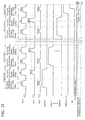
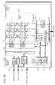
- FIG. 46 is a graph plotting a dependency of a forming start voltage on a transition metal oxide film thickness which is disclosed in Non-Patent Reference 1.
- the graph indicates four kinds of properties, NiO, TiO 1 , HfO 2 , and ZrO 2 , as transition metal oxides.
- the forming start voltage depends on the kinds of the transition metal oxides. When a thickness of a transition metal oxide is greater, the forming start voltage is higher. Therefore, in order to decrease the forming voltage, it is preferable to select a transition metal oxide such as NiO to form a transition metal oxide film having a small thickness.
- the “forming voltage” refers to a voltage applied to perform a forming for a variable resistance element.
- the “forming start voltage” refers to the lowest voltage (a forming voltage having a minimum absolute value) required to perform a forming for a variable resistance element
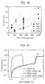
- FIG. 47 is a graph plotting current-voltage (I-V) properties which indicates unipolar resistance change properties of NiO which is disclosed in Non-Patent Reference 1.
- I-V current-voltage
- a solid line represents resistance change hysteresis before baking of 150° C. and 300 hours
- a broken line represents resistance change hysteresis after the baking of 150° C. and 300 hours.
- the resistance change hysteresis is not notably changed, even if the resistance change hysteresis is repeatedly looped by changing a voltage in the case where a voltage applied to the variable resistance element is limited after the point A where a high resistance state is changed to a low resistance state. Therefore, the high resistance state and the low resistance state are achieved with stability.
- Patent Reference 1 discloses an ion conduction nonvolatile memory device using a rare-earth oxide thin film as a variable resistance elements.
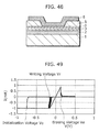
- FIG. 48 is a cross-sectional view of a memory cell disclosed in Patent Reference 1.
- This memory cell has the following structure.
- a lower electrode 2 is formed on a substrate 1 having a high electrical conductivity (a silicon substrate 1 doped with a P-type high-concentration impurity, for example).
- An ion source layer 3 including a metallic element as an ion source is formed on the lower electrode 2 .
- a memory layer 4 having a relatively high resistance value is formed on the ion source layer 3 .
- An upper electrode 6 is formed to contact the memory layer 4 through an opening in an insulation layer 5 on the memory layer 4 .
- Patent Reference 1 discloses CuTe, GeSbTe, AgGeTe, and the like as a material of the ion source layer 3 , and discloses a rear-earth element oxide such as a gadolinium oxide as a material of the memory layer 4 .
- a material of the lower electrode 2 and the upper electrode 6 is described as a common semiconductor line material such as TiW and TaN.
- a gadolinium oxide for the memory layer 4 is added with metallic particles such as Cu having an amount not enough to form a layer, namely, an amount enough to keep insulation properties or semi-insulation properties.
- a method of writing data into the memory cell shown in FIG. 48 is as follows.
- a negative voltage causing a potential of the upper electrode 6 to be lower than a potential of the lower electrode 2 a conducting path including a large amount of metallic elements is formed in the memory layer 4 , or a large number of defects resulting from the metallic elements are formed in the memory layer 4 .
- a resistance value of the memory layer 4 is decreased.
- the conducting path or the defects formed in the memory layer 4 due to the metallic elements disappear. As a result, the resistance value of the memory layer 4 is increased.
- FIG. 49 is a graph plotting I-V properties changed from an initial state regarding the memory cell shown in FIG. 48 .
- a relatively high negative voltage is applied to the memory cell to change a high resistance state of the initial state to a low resistance state.
- the voltage is assumed to be an initialization voltage Vo.
- an erasing voltage Ve is applied to the memory cell to change the low resistance state to a high resistance state.
- a writing voltage Vr having an absolute value smaller than that of the initialization voltage Vo is applied to the memory cell to change the high resistance state to a low resistance state.
- Patent Reference 1 discloses a technology of lowering the initialization (forming) voltage.
- the addition of metallic particles to the memory layer 4 forms defects in the memory layer 4 .
- a low voltage easily allows ion of the metallic elements to start moving.
- new ion is moved from the ion source layer 3 in contact with the memory layer 4 .
- Such ion movements continuously occur, speedily forming a conducting path.
- the conducting path allows an initialization (forming) operation to be performed by a low voltage. As a result, reliability of the memory cell can be maintained.
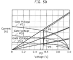
- Patent Reference 2 discloses a method of writing multiple values into a 1T1R memory cell using a variable resistance memory element.
- FIG. 50 is a graph for explaining analysis of an operation point for low resistance writing (LR writing operation point analysis) based on static properties between a Metal Insulator Semiconductor (MIS) transistor and a variable resistance element in such a 1T1R cell. As shown in FIG. 50 , the I-V properties of the variable resistance element are represented by straight lines. When a voltage higher than a threshold voltage Vth for writing data to cause a low resistance state (hereinafter, referred to as “LR writing”) is applied to the variable resistance element, a high resistance state of the variable resistance element is changed to a low resistance state.
- Vth a threshold voltage
- a gate voltage VGS of the MIS transistor when sequentially changed to VG 3 , VG 2 , and then VG 1 (where VG 3 ⁇ VG 2 ⁇ VG 1 ), the I-V properties of the MIS transistor is changed. If the gate voltage VGS of the MIS transistor is higher, more current flows and on-resistance is lower.
- the change of the gate voltage VGS of the MIS transistor sequentially to VG 3 , VG 2 , and then VG 1 also changes the LR writing operation point sequentially to P 3 , P 2 , and then P 1 , so that the variable resistance element has a low resistance value corresponding to a value of current flowing at the operation point.
- a level of the low resistance value of the variable resistance element controls the gate voltage VGS of the MIS transistor, and thereby controls its I-V properties so as to flexibly set the I-V properties.
- the method can therefore be used for multivalued memories.
- Patent Reference 3 discloses a method of writing multiple values to a variable resistance element.
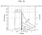
- FIG. 51 is a graph plotting resistance-voltage (R-V) characteristics of a metal insulation film (magnesium oxidation film, for example) serving as the variable resistance element.
- FIG. 51 shows resistance change characteristics (a) causing the variable resistance element to change into a high resistance state by applying a positive voltage (hereinafter, writing to change the variable resistance element into a high resistance state is referred to as “high resistance (HR) writing”), and (b) causing the variable resistance element to change into a low resistance state by applying a negative voltage (hereinafter, writing to change the variable resistance element into a low resistance state is referred to as “low resistance (LR) writing”).
- HR positive voltage
- LR negative voltage
- Patent Reference 3 discloses that a level of a high resistance value of a variable resistance element can be set to a desired high resistance value, by setting a plurality of switching voltages to control the R-V characteristics.
- Non-Patent Reference 1 discloses the following. Some kinds of transition metal oxides show nonvolatile variable change phenomenon due to application of electrical pulse. The occurrence of the variable change phenomenon firstly requires application of a voltage having an absolute value greater than an absolute value of a control voltage for subsequent resistance change. This is explained using a model of forming a conducting path at a level enough to cause resistance change from an extremely high resistance state in an initial insulation state. Non-Patent Reference 1 also discloses that, after the forming, variable resistance elements using these transition metal oxides produce reversible resistance change when electrical signals exceeding a predetermined threshold voltage are applied.
- Non-Patent Reference 1 further discloses that there are two types of such a variable resistance element: an unipolar variable resistance element that can be controlled only by applying a voltage having a polarity of a single direction; and a bipolar variable resistance element that can be controlled by applying voltages having different polarities.
- Patent Reference 1 discloses that even an ion conductive variable resistance element made of a material that is not a transition metal oxide is also capable of achieving the same resistance change caused by a forming or electrical pulse.
- Patent Reference 2 discloses a method of controlling LR writing of a variable resistance element.
- Patent Reference 2 discloses that a high resistance state of a variable resistance element is changed to a low resistance state when an applied voltage reaches a predetermined voltage, that a resistance value of a low resistance state is determined depending on a size of an amount of current flowing in the variable resistance element, and that the control method can be used for multivalued memories by using the above phenomenon to control a gate voltage.
- Patent Reference 3 reports that there is a phenomenon that a level of a high resistance value is uniquely determined by a value of a voltage applied to a variable resistance value in writing data to cause a high resistance state (hereinafter, referred to as “HR writing”).
- variable resistance nonvolatile memory element is capable of having a simple structure in which some materials such as transition metal oxides are sandwiched between electrodes.
- the prior arts also disclose that a forming using a high voltage is initially performed for the structure so as to achieve stable control of a change between a low resistance state and a high resistance state only by afterwards applying electrical signals having a short pulse.
- the prior arts further disclose that the low resistance state and the high resistance state are nonvolatile. If these variable resistance nonvolatile memory elements are used as memory cells, it would be possible to offer memories having a higher speed and a lower cost more than commonly-known nonvolatile memories such as Flash memory.
- tantalum that is one of transition metals for an example of a material of variable resistance nonvolatile memory devices, in order to provide a variable resistance nonvolatile memory device including memory cells each having a variable resistance layer comprising the oxygen-deficient oxide (tantalum oxide) and a switch element.
- the oxygen-deficient oxide refers to an oxide in which oxygen is deficient in a stoichiometric composition.
- Ta 2 O 5 is an example of an oxide having a stoichiometric composition.
- the Ta 2 O 5 contains oxygen 2.5 times as much as oxygen in tantalum, which is expressed by an oxygen content percentage as 71.4%. If an oxide having an oxygen content percentage lower than 71.4% is expressed as TaO x , a tantalum oxide (hereinafter, referred to as “Ta oxide”) having a nonstoichiometric composition satisfying 0 ⁇ x ⁇ 2.5 is called an oxygen-deficient Ta oxide.
- a good resistance change operation can be obtained within 0.8 ⁇ x ⁇ 1.9 that is a desirable range for x.
- variable resistance element having a variable resistance layer comprising an oxygen-deficient Ta oxide (TaO 1.54 ).
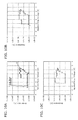
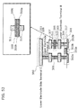
- FIG. 52 is a cross-sectional view of a structure (structure for one bit) of a 1T1R memory cell using a conventional variable resistance element.
- the 1T1R memory cell 500 includes a transistor 317 and a variable resistance element 300 .
- a first N-type diffusion layer region 302 a On a semiconductor substrate 301 , sequentially formed are a first N-type diffusion layer region 302 a , a second N-type diffusion layer region 302 b , a gate insulation film 303 a , a gate electrode 303 b , a first via 304 , a first line layer 305 , a first resistance film via 510 , a variable resistance element 300 , a second resistance film via 511 , a second via 306 , a second line layer 307 , a third via 308 , and a third line layer 311 .
- the second line layer 307 connected to the second resistance film via 511 is defined as an upper electrode terminal A
- the first line layer 305 connected to the first resistance film via 510 is defined as a lower electrode terminal B
- the third line layer 311 is defined as a lower electrode side terminal C.
- a voltage of the semiconductor substrate 301 is 0 V, which is supplied from a commonly-known structure of a 0V power source line (not shown).
- the figure located at the upper right corner of FIG. 52 is an enlarged view of the variable resistance element 300 .
- the variable resistance element 300 has a structure in which a set of the lower electrode 300 a , the variable resistance layer 300 b that is the oxygen-deficient Ta oxide (TaO 1.54 ), and the upper electrode 300 c is sandwiched between the first resistance film via 510 and the second resistance film via 511 .
- the set is on the first resistance film via 510 and is in contact with the second resistance film via 511 connected to the second line layer 307 .
- an N-channel Metal Oxide Semiconductor (NMOS) transistor has a gate width W of 0.44 ⁇ m and a gate length L of 0.18 ⁇ m, and the gate insulation film 303 a has a thickness Tox of 3.5 nm.
- NMOS Metal Oxide Semiconductor
- the lower electrode 300 a comprises TaN.
- the upper electrode 300 c comprises electrode materials including, as a major component, Pt that is likely to occur resistance change.
- the variable resistance element 300 has the following resistance change characteristics.
- a positive voltage equal to or higher than a threshold voltage causing resistance change is applied to the upper electrode 300 c with reference to the lower electrode 300 a .
- oxidation occurs at an interface of the upper electrode 300 c so as to change the variable resistance element 300 from a low resistance state to a high resistance state.
- a negative voltage equal to or lower than the threshold voltage causing resistance change is applied to the upper electrode 300 c with reference to the lower electrode 300 a , reductive reaction occurs in the variable resistance layer 300 b close to the interface of the upper electrode 300 c so as to change the variable resistance element 300 from the high resistance state to a low resistance state.
- variable resistance element 300 has different electrode structure, in which the material of the upper electrode 300 c is different from the material of the lower electrode 300 a .
- a relationship between (a) each of a high resistance state and a low resistance state and (b) a polarity direction of an applied pulse voltage is therefore uniquely determined depending on an electrode material.
- the variable resistance element 300 is capable of havingreversible and stable rewriting characteristics and employing the resistance change phenomenon.
- Such a nonvolatile memory element is an object of the inventors of this application, and is described in detail in PCT International Publication No. WO2009/050833 (Patent Reference 5) that is a patent reference related to this application.
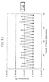
- FIG. 53 is a graph plotting a resistance value (a resistance measurement voltage is 0.4 V) of each application of a voltage to the 1T1R memory cell 500 shown in FIG. 52 , in the case that a pulse voltage causing LR writing and a pulse voltage causing HR writing is alternately applied for a certain one bit after initially performing a forming by applying a high voltage pulse.
- a horizontal axis represents a count of applied electrical pulse, while a vertical axis represents a resistance value.
- the resistance measurement voltage is a voltage applied to the variable resistance element in order to measure a resistance value of the variable resistance element. This resistance measurement voltage is equal to or lower than a threshold voltage causing resistance change (change between a high resistance state and a low resistance state).
- FIG. 53 shows the following. Since a gate voltage Vg of 2.4 V is applied to the gate electrode 303 b in the 1T1R memory cell 500 shown in FIG. 52 , the 1T1R memory cell 500 is firstly in a low resistance state LR of approximately 8.8 k ⁇ . Then, a pulse voltage of +2.4 V (with a pulse width of 50 ns) is applied to the upper electrode terminal A (here, a ground potential is applied to the lower electrode side terminal C), in other words, a positive pulse voltage of +2.4 V is applied, so that the low resistance state LR is changed to a high resistance state HR of approximately 222 k ⁇ .
- Vg 2.4 V
- a pulse voltage of +2.4 V (with a pulse width of 50 ns) is applied to the lower electrode side terminal C (here, a ground potential is applied to the upper electrode terminal A); in other words, a negative pulse voltage of ⁇ 2.4 V is applied; so that the high resistance state HR is changed to a low resistance state LR of approximately 8.9 k ⁇ .
- HR writing caused by application of a positive pulse voltage to the upper electrode terminal A for the lower electrode side terminal C and (b) LR writing caused by application of a negative pulse voltage to the upper electrode terminal A for the lower electrode side terminal C are repeated.
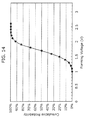
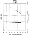
- FIG. 54 is a graph plotting normalized expectation values of resistance values of a high resistance state HR and a low resistance state LR in the case that a pulse application count is further increased (application of a positive pulse 300 times and application of a negative pulse 300 times) in FIG. 53 .
- a horizontal axis represents resistance values of HR and LR (a resistance measurement voltage is 0.4 V), while a vertical axis represents a normalized expectation value that indicates a degree of variation of the resistance values when the resistance values are fitted in normal distribution.
- each of the high resistance state and the low resistance state is not set to have the same resistance value, but set to have certain statistical distribution variation.
- the discovered phenomenon is not conventionally known. Especially, variation in resistance values in the high resistance state is large. Therefore, it is important in a reading operation how to maximize a window C defined by a minimum value of the high resistance state HR and a maximum value of the low resistance state LR when a variable resistance memory device has variable resistance memory elements.
- a window C becomes narrower, which produces serious problems such as reading errors and decrease of a reading speed, failing stable operations.
- An object of the present invention is to provide a forming method optimum for a variable resistance element to maximize an operation window of the variable resistance element, and also to provide a variable resistance nonvolatile memory device having a function of such a forming method.
- variable resistance nonvolatile memory element forming method of performing a forming for a variable resistance nonvolatile memory element, the forming being initialization to change the variable resistance nonvolatile memory element from a first state to a second state, the first state being a state after manufacturing the variable resistance nonvolatile memory element, and the second state being a state reversibly changeable between a high resistance state and a low resistance state depending on a polarity of an applied voltage pulse, wherein the variable resistance nonvolatile memory element has a resistance value that is higher in the first state than in the high resistance state, the method including: determining whether or not the resistance value of the variable resistance nonvolatile memory element is lower than the resistance value in the high resistance state; and applying a voltage pulse of a voltage to the variable resistance nonvolatile memory element, when the determination is made that the resistance value of the variable resistance nonvolatile memory element is not lower than the resistance value in the high resistance state, the voltage
- a voltage applied in a forming is restricted within a certain range (within a range of the forming start voltage added with a certain margin). Therefore, in comparison to the situation where a forming is performed by applying a voltage exceeding the range, the above method can offer a resistance value (a high resistance value level) that is higher and less likely to depend on the applied voltage when HR writing is performed for the variable resistance nonvolatile memory element after the forming. As a result, an operation window of the variable resistance nonvolatile memory element can be expanded.
- variable resistance nonvolatile memory element includes a first oxygen-deficient transition metal oxide layer and a second oxygen-deficient transition metal oxide layer, the second oxygen-deficient transition metal oxide layer having an oxygen content percentage higher than an oxygen content percentage of the first oxygen-deficient transition metal oxide layer, in the applying, a voltage pulse having a positive voltage is applied to the first oxygen-deficient transition metal oxide layer, with reference to a potential of the second oxygen-deficient transition metal oxide layer, and the predetermined voltage has a value determined depending on the first and second oxygen-deficient transition metal oxide layers.
- the first oxygen-deficient transition metal oxide layer is a layer including a composition represented by TaO x
- the second oxygen-deficient transition metal oxide layer is a layer including a composition represented by TaO y , where x ⁇ y, and the predetermined voltage is 0.7 V.
- the determining and the applying are repeated, and in the applying, the voltage pulse applied to the variable resistance nonvolatile memory element has the voltage, an absolute value of the voltage being greater than an absolute value of a voltage of a voltage pulse applied immediately prior to the applying.
- the voltage pulse applied to the variable resistance nonvolatile memory element has the voltage that is a sum of the voltage of the voltage pulse applied immediately prior to the applying and a voltage not exceeding the predetermined voltage.
- an increment of voltages to be gradually increased is set to be a voltage (for example, 0.1 V) lower than the above-described margin.
- variable resistance nonvolatile memory element is provided in each of a plurality of memory cells, and in the applying, a voltage pulse of a voltage having an absolute value greater than the absolute value of the voltage of the voltage pulse applied immediately prior to the applying is applied to each of variable resistance nonvolatile memory elements including the variable resistance nonvolatile memory element which are respectively provided in the plurality of memory cells, after applying a voltage pulse having a same voltage sequentially to the variable resistance nonvolatile memory elements.
- the forming is performed for the plurality of memory cells by applying an optimum voltage depending on each of the variable resistance nonvolatile memory elements.
- the voltage pulse is applied using a voltage source having a limited maximum value of a supplyable current.
- a voltage source is set so that an optimum forming voltage is applied to the variable resistance nonvolatile memory element when the voltage source causes flow of a maximum supplyable current.
- a forming can be completed by applying a voltage once, without applying voltages a plurality of times step by step.
- variable resistance nonvolatile memory device including variable resistance nonvolatile memory elements
- the variable resistance nonvolatile memory device including: a memory cell array including a plurality of memory cells in each of which a corresponding one of the variable resistance nonvolatile memory elements is connected in series to a corresponding one of switch elements, the variable resistance nonvolatile memory elements each being reversibly changeable between a high resistance state and a low resistance state depending on a polarity of an applied voltage pulse; a selection unit configured to select at least a memory cell from the memory cell array; a forming voltage pulse generation unit configured to generate a forming voltage pulse to be applied to change the variable resistance nonvolatile memory element in the memory cell selected by the selection unit from a first state to a second state, the first state being a state after manufacturing the variable resistance nonvolatile memory element and having a resistance value higher than a resistance value in the high resistance state, and the second state being a state reversibly changeable between the
- a voltage applied in a forming is restricted within a certain range (within a range of the forming start voltage added with a certain margin). Therefore, in comparison to the situation where a forming is performed by applying a voltage exceeding the range, the above method can offer a resistance value (a high resistance value level) that is higher and less likely to depend on the applied voltage when HR writing is performed for the variable resistance nonvolatile memory element after the forming. As a result, an operation window of the variable resistance nonvolatile memory element can be expanded.
- each of the variable resistance nonvolatile memory elements includes a first oxygen-deficient transition metal oxide layer and a second oxygen-deficient transition metal oxide layer, the second oxygen-deficient transition metal oxide layer having an oxygen content percentage higher than an oxygen content percentage of the first oxygen-deficient transition metal oxide layer, the forming voltage pulse generation unit is configured to apply a voltage pulse having a positive voltage to the first oxygen-deficient transition metal oxide layer, with reference to a potential of the second oxygen-deficient transition metal oxide layer, and the predetermined voltage has a value determined depending on the first and second oxygen-deficient transition metal oxide layers.
- the first oxygen-deficient transition metal oxide layer is a layer including a composition represented by TaO x
- the second oxygen-deficient transition metal oxide layer is a layer including a composition represented by TaO y , where x ⁇ y, and the predetermined voltage is 0.7 V.
- the forming voltage pulse generation unit includes a variable voltage pulse generation circuit which generates a voltage pulse of a voltage having an absolute value gradually increased.
- the variable voltage pulse generation circuit generates a next voltage pulse having a voltage that is a sum of a voltage of a voltage pulse applied immediately prior to application of the next voltage pulse and a voltage not exceeding the predetermined voltage.
- an increment of voltages to be gradually increased is set to be a voltage (for example, 0.1 V) equal to or lower than 0.7 V.
- the forming voltage pulse generation unit is configured to generate the voltage pulse using a voltage source having a limited maximum value of a supplyable current.
- a voltage source is set so that an optimum forming voltage is applied to the variable resistance nonvolatile memory element when the voltage source causes flow of a maximum supplyable current.
- a forming can be completed by applying a voltage once, without applying voltages a plurality of times step by step.
- variable resistance nonvolatile memory device further includes a plurality of bit lines and a plurality of source lines, wherein each of the plurality of memory cells is connected between a corresponding one of the plurality of bit lines and a corresponding one of the plurality of source lines
- the selection unit includes a row selection unit and a column selection unit, the row selection unit configured to select at least one of the plurality of source lines, and the column selection unit configured to select at least one of the plurality of bit lines
- the reading circuit is connected to the variable resistance nonvolatile memory elements via the column selection unit
- the forming voltage pulse generation unit is configured to (i) apply the forming voltage pulse to the at least one of the plurality of source lines selected by the row selection unit with reference to a potential of the at least one of the plurality of bit lines selected by the column selection unit, or (ii) apply the forming voltage pulse to the at least one of the plurality of bit lines selected by the column selection unit with reference to a potential of the at least one of the pluralit
- variable resistance nonvolatile memory device further includes an automatic forming control circuit, which controls the row selection unit, the column selection unit, and the forming voltage pulse generation unit to sequentially select the plurality of memory cells and apply the forming voltage pulse to the variable resistance nonvolatile memory element in the selected one of the plurality of memory cells.
- the forming is performed for the plurality of memory cells by applying an optimum voltage depending on each of the variable resistance nonvolatile memory elements.
- the forming voltage pulse generation unit has a terminal and is configured to generate a voltage pulse received via the terminal as the forming voltage pulse, the terminal receiving, from outside, the voltage pulse that has an absolute value not exceeding the maximum absolute value of the absolute value maximum voltage.
- a forming voltage pulse provided from an external device, such as an IC tester can be applied to the variable resistance nonvolatile memory element in each of the memory cells.
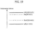
- the reading unit including: a forming reference resistance used to determine whether or not the variable resistance nonvolatile memory element currently has a resistance value lower than a resistance value in the high resistance state; a reading reference resistance used to determine whether the variable resistance nonvolatile memory element is in the high resistance state or in the low resistance state; a selection circuit which selects one of the forming reference resistance and the reading reference resistance; and a comparison circuit which compares a reference current to a memory cell current, the reference current flowing when a certain voltage is applied to one of the forming reference resistance and the reading reference resistance which is selected by the selection circuit, and the memory cell current flowing when the certain voltage is applied to the variable resistance nonvolatile memory element.
- a resistance value of the forming reference resistance is higher than a resistance value of the reading reference resistance. This is because the determination as to whether a forming is completed can be made based on the resistance value in the high resistance state in order to determine whether or not a current resistance value of the variable resistance nonvolatile memory element is lower than the resistance value in the high resistance state, while the determination as to whether the high resistance state or the low resistance state needs to be made based on a resistance value within the operation window.
- the forming method for the variable resistance nonvolatile memory element and the variable resistance nonvolatile memory device according to the present invention perform a forming for each memory cell to change an initial state having a high resistance value, thereby preventing excess current from flowing in the variable resistance element after the forming.
- a changeable high resistance value level it is possible to control a changeable high resistance value level to be higher, thereby expanding an operation window between a low resistance state and a high resistance state.
- a high-speed reading and data reliability can be improved, and a risk of erroneous reading can be significantly reduced.
- FIG. 1 is a schematic diagram showing a basic structure of a nonvolatile memory element according to basic data of the present invention.
- FIG. 2 is a block diagram showing a structure of a variable resistance element added with a fixed resistance according to basic data 1 of the present invention.
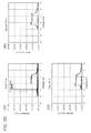
- Each of (a 1 ) to (a 3 ) in FIG. 3A is a graph plotting a relationship between a resistance value and an applied pulse voltage according to the basic data of the present invention.
- Each of (b 1 ) to (b 3 ) in FIG. 3B is a graph plotting a relationship between a resistance value and an applied pulse voltage according to the basic data of the present invention.
- Each of (c 1 ) to (c 3 ) in FIG. 3C is a graph plotting a relationship between a resistance value and an applied pulse voltage according to the basic data of the present invention.
- Each of (d 1 ) to (d 3 ) in FIG. 3D is a graph plotting a relationship between a resistance value and an applied pulse voltage according to the basic data of the present invention.
- Each of (e 1 ) to (e 3 ) in FIG. 3E is a graph plotting a relationship between a resistance value and an applied pulse voltage according to the basic data of the present invention.
- FIG. 4 is a flowchart of measurement of the pulse RV characteristics according to the basic data of the present invention.
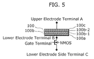
- FIG. 5 is a block diagram showing a structure of a 1T1R memory cell according to the basic data of the present invention.
- FIG.6A is a cross-sectional view of one of two kinds of a basic memory cell structure of the 1T1R memory cell according to the basic data of the present invention.
- FIG. 6B is a cross-sectional view of the other one of the two kinds of the basic memory cell structure of the 1T1R memory cell according to the basic data of the present invention.
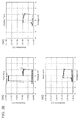
- FIG. 7A is a graph plotting a relationship between a resistance value and an applied pulse voltage regarding the 1T1R memory cell according to the basic data of the present invention.
- FIG. 7B is a graph plotting a relationship between a resistance value and an applied pulse voltage regarding the 1T1R memory cell according to the basic data of the present invention.
- FIG. 7C is a graph plotting a relationship between a resistance value and an applied pulse voltage regarding the 1T1R memory cell according to the basic data of the present invention.
- FIG. 8A is a graph plotting a relationship between a resistance value and an applied pulse voltage regarding the 1T1R memory cell according to the basic data of the present invention.
- FIG. 8B is a graph plotting a relationship between a resistance value and an applied pulse voltage regarding the 1T1R memory cell according to the basic data of the present invention.
- FIG. 8C is a graph plotting a relationship between a resistance value and an applied pulse voltage regarding the 1T1R memory cell according to the basic data of the present invention.
- FIG. 9 is a graph plotting a relationship between a resistance value and an electrical pulse application count regarding the 1T1R memory cell according to the basic data of the present invention.
- FIG. 10A is a graph plotting a relationship between a resistance value and an applied pulse voltage when the soft forming is performed for the 1T1R memory cell according to the basic data of the present invention.
- FIG. 10B is a graph plotting a relationship between a resistance value and an applied pulse voltage when the soft forming is performed for the 1T1R memory cell according to the basic data of the present invention.
- FIG. 10C is a graph plotting a relationship between a resistance value and an applied pulse voltage when the soft forming is performed for the 1T1R memory cell according to the basic data of the present invention.
- FIG. 11 is a graph plotting a relationship between a resistance value and an electrical pulse application count when the soft forming is performed for the 1T1R memory cell according to the basic data of the present invention.
- FIG. 12A is a schematic diagram of a memory cell including a variable resistance element satisfying structural requirements according to the basic data of the present invention.
- FIG. 12B is a schematic diagram of a memory cell including a variable resistance element satisfying structural requirements according to the basic data of the present invention.
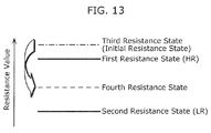
- FIG.13 is a diagram for explaining relationships among respective resistance states in a forming according to the basic data of the present invention.
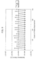
- FIG. 14 is a graph plotting cumulative probability distribution of a forming voltage Vb according to the basic data of the present invention.
- FIG. 15 is a diagram for explaining an estimation mechanism of the soft forming according to the basic data of the present invention.
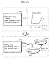
- FIG. 16 is a diagram for explaining a writing method according to the basic data of the present invention.
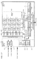
- FIG.17 is a block diagram showing a structure of a variable resistance nonvolatile memory device according to a first embodiment of the present invention.
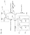
- FIG. 18 is a circuit diagram showing an example of a structure of a sense amplifier according to according to the first embodiment of the present invention.
- FIG. 19 is a diagram for explaining determination levels of the sense amplifier according to the first embodiment of the present invention.
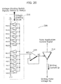
- FIG. 20 is a circuit diagram showing an example of a structure of a writing circuit according to the first embodiment of the present invention.
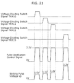
- FIG. 21 is a timing diagram showing a waveform of step-up writing pulse voltage application according to the first embodiment of the present invention.
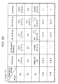
- FIG. 22 is a list of setting voltages of each node for respective operation modes according to the first embodiment of the present invention.
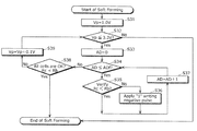
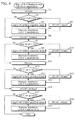
- FIG. 23 is a flowchart of the soft forming performed by the variable resistance nonvolatile memory device according to the first embodiment of the present invention.
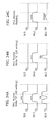
- FIG. 24A is a timing diagram of an operation performed by the variable resistance nonvolatile memory device according to the first embodiment of the present invention.
- FIG. 24B is a timing diagram of an operation performed by the variable resistance nonvolatile memory device according to the first embodiment of the present invention.
- FIG. 24C is a timing diagram of an operation performed by the variable resistance nonvolatile memory device according to the first embodiment of the present invention.
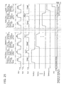
- FIG. 25 is a timing diagram of the soft forming performed by the variable resistance nonvolatile memory device according to the first embodiment of the present invention.
- FIG. 26 is a block diagram showing a structure of a variable resistance nonvolatile memory device according to a second embodiment of the present invention.
- FIG. 27 is a circuit diagram showing an example of a structure of a variable voltage generation circuit according to the second embodiment of the present invention.
- FIG. 28 is a timing diagram showing a waveform of step-up writing pulse voltage application according to the second embodiment of the present invention.
- FIG. 29 is a list of setting voltages of each node for respective operation modes according to the second embodiment of the present invention.
- FIG. 30A is a timing diagram of an operation performed by the variable resistance nonvolatile memory device according to the second embodiment of the present invention.
- FIG. 30B is a timing diagram of an operation performed by the variable resistance nonvolatile memory device according to the second embodiment of the present invention.
- FIG. 30C is a timing diagram of an operation performed by the variable resistance nonvolatile memory device according to the second embodiment of the present invention.
- FIG. 31 is a timing diagram of the soft forming performed by the variable resistance nonvolatile memory device according to the second embodiment of the present invention.
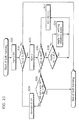
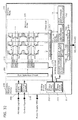
- FIG. 32 is a block diagram showing a structure of a variable resistance nonvolatile memory device according to a third embodiment of the present invention.
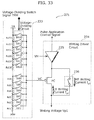
- FIG. 33 is a circuit diagram showing an example of a structure of a writing circuit according to the third embodiment of the present invention.
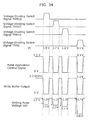
- FIG. 34 is a timing diagram showing a waveform of step-down writing pulse voltage application according to the third embodiment of the present invention.
- FIG. 35 is a list of setting voltages of each node for respective operation modes according to the third embodiment of the present invention.
- FIG. 36 is a flowchart of the soft forming performed by the variable resistance nonvolatile memory device according to the third embodiment of the present invention.
- FIG. 37A is a timing diagram of an operation performed by the variable resistance nonvolatile memory device according, to the third embodiment of the present invention.
- FIG. 37B is a timing diagram of an operation performed by the variable resistance nonvolatile memory device according to the third embodiment of the present invention.
- FIG. 37C is a timing diagram of an operation performed by the variable resistance nonvolatile memory device according to the third embodiment of the present invention.
- FIG. 38 is a timing diagram of the soft forming performed by the variable resistance nonvolatile memory device according to the third embodiment of the present invention.
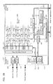
- FIG. 39 is a block diagram showing a structure of a variable resistance nonvolatile memory device according to a fourth embodiment of the present invention.
- FIG. 40 is a block diagram showing a structure of a variable resistance nonvolatile memory device according to a fifth embodiment of the present invention.
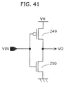
- FIG. 41 is a circuit diagram showing an example of a structure of a forming circuit according to the fifth embodiment of the present invention.
- FIG. 42A is a circuit diagram for explaining an operation of a forming circuit according to the fifth embodiment of the present invention.
- FIG. 42B is a circuit diagram for explaining an operation of the forming circuit according to the fifth embodiment of the present invention.
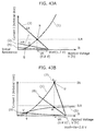
- FIG. 43A is a graph plotting I-V properties used in operation point analysis in a forming according to the fifth embodiment of the present invention.
- FIG. 43B is a graph plotting I-V properties used in operation point analysis in a forming according to the fifth embodiment of the present invention.
- FIG. 44A is a timing diagram of an operation performed by the variable resistance nonvolatile memory device according to the fifth embodiment of the present invention.
- FIG. 44B is a timing diagram of an operation performed by the variable resistance nonvolatile memory device according to the fifth embodiment of the present invention.
- FIG. 44C is a timing diagram of an operation performed by the variable resistance nonvolatile memory device according to the fifth embodiment of the present invention.
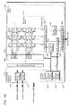
- FIG. 45 is a block diagram showing a structure of a variable resistance nonvolatile memory device according to a sixth embodiment of the present invention.
- FIG. 46 is a graph plotting a dependency of a forming voltage on a transition metal oxide film thickness according to a conventional variable resistance nonvolatile memory.
- FIG. 47 is a graph plotting I-V properties according to the conventional variable resistance nonvolatile memory.
- FIG. 48 is a cross-sectional view of a memory cell according to a conventional variable resistance nonvolatile memory element.
- FIG. 49 is a graph plotting I-V properties changed from an initial state according to the conventional variable resistance nonvolatile memory element.
- FIG. 50 is a graph for explaining LR writing operation point analysis based on static properties between a MIS transistor and a variable resistance element in a conventional 1T1R cell.
- FIG. 51 is a graph plotting resistance-voltage characteristics in the case that a plurality of switching voltages are set for a conventional variable resistance element.
- FIG. 52 is a cross-sectional view of a conventional 1T1R memory cell.
- FIG. 53 is a graph showing a relationship between a resistance value and an electrical pulse application count according to the conventional 1T1R memory cell.
- FIG. 54 is a graph showing a relationship between a resistance value and a normalized expectation value regarding a pulse change according to the conventional 1T1R memory cell.
- a variable resistance nonvolatile memory device is a 1T1R nonvolatile memory device in which each variable resistance element is connected in series to a MOS transistor.
- the variable resistance nonvolatile memory device according to the first embodiment can perform a forming method (namely, a forming) capable of controlling a high resistance value level of the variable resistance element.
- the variable resistance nonvolatile memory device can apply an optimum pulse voltage for HR writing to the variable resistance element. As a result, this variable resistance nonvolatile memory device can provide a wide operation window between a high resistance state and a low resistance state.
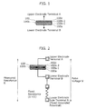
- FIG. 1 is a schematic diagram showing a basic structure of a variable resistance element used in an experiment.
- a variable resistance element 100 has a structure in which a lower electrode 100 a , a variable resistance layer 100 b , and an upper electrode 100 c are sequentially stacked to form a sandwich shape.
- a lower electrode terminal B extends from the lower electrode 100 a
- an upper electrode terminal A extends form the upper electrode 100 c.
- the lower electrode 100 a comprises TaN
- the upper electrode 100 c comprises electrode materials including, as a major component, Pt that is likely to occur resistance change.
- the second oxygen-deficient tantalum oxide layer 100 b - 2 (TaO 2.47 ) is formed by performing, prior to a process for manufacturing the upper electrode 100 c , a plasma oxidation process on a surface of the first oxygen-deficient tantalum oxide layer 100 b - 1 (TaO 1.54 ) formed by sputtering. Therefore, the second oxygen-deficient tantalum oxide layer 100 b - 2 (TaO 2.47 ) has an oxygen content percentage higher than that of the first oxygen-deficient tantalum oxide layer 100 b - 1 (TaO 1.54 ).
- the second oxygen-deficient tantalum oxide layer 100 b - 2 (TaO 2.47 ) has a resistance value higher than that of the first oxygen-deficient tantalum oxide layer 100 b -i (TaO 1.54 ). Since the variable resistance element 100 therefore has a significantly high initial resistance (>10 M ⁇ ), resistance change needs application of a high forming voltage (voltage for LR writing) to form a conducting path.
- the variable resistance element 100 has the following resistance change characteristics.
- a positive voltage equal to or higher than a threshold voltage causing resistance change is applied to the upper electrode 100 c with reference to the lower electrode 100 a .
- oxidation occurs at an interface of the upper electrode 100 c so as to change the variable resistance element 100 from a low resistance state to a high resistance state.
- a negative voltage equal to or lower than the threshold voltage causing resistance change is applied to the upper electrode 100 c with reference to the lower electrode 100 a , reductive reaction occurs at an interface of the upper electrode 100 c so as to change the variable resistance element 100 from a high resistance state to a low resistance state.
- variable resistance element 100 including such a high resistance layer (TaO 2.47 ) has been invented by the inventors of this application, aiming at providing a nonvolatile memory element that has reversible stable rewriting characteristics and that utilizes resistance change phenomenon.
- the variable resistance element 100 is discloses in detail in PCT International Publication No. WO2010/021134 (Patent Reference 6) that is a patent reference related to this application.
- Table 1 lists: a size of the variable resistance element 100 used in the experiment; a thickness and an oxygen content percentage x of the first tantalum oxide layer (TaO x layer); and a thickness and an oxygen content percentage y of the second tantalum oxide layer (TaO y layer).
- FIG. 2 is a circuit diagram of an evaluation circuit for the experiment.
- the evaluation circuit has a cell structure in which the variable resistance element 100 shown in FIG. 1 is connected in series to a fixed resistance element of 1 k ⁇ .
- the same reference numerals of FIG. 1 are assigned to the identical structural elements of FIG. 2 , so that the identical structural elements are not explained again below.
- the evaluation circuit shown in FIG. 2 has a cell structure for obtaining basic data.
- the evaluation circuit has a pseudo structure in which a fixed resistance of 1 k ⁇ is used as a substitute for the memory transistor.
- a terminal of the fixed resistance element which is not connected to the variable resistance element 100 serves as a lower electrode side terminal D.
- FIG. 3E is a graph plotting pulse application R-V characteristics changed from an initial state of the variable resistance element when a voltage pulse is applied to the evaluation circuit under various conditions in the evaluation circuit shown in FIG. 2 .
- Each of the graphs plots characteristics of a state of a resistance value after applying a predetermined pulse. The characteristics are hereinafter referred to also as pulse RV characteristics.
- a horizontal axis represents a pulse voltage V (with a pulse width of 100 ns) applied between the upper electrode terminal A and the lower electrode side terminal D in the evaluation circuit shown in FIG. 2 .
- the lower electrode side terminal D has a fixed ground potential.
- positive pulse voltage application while application of a negative voltage to the upper electrode terminal A with reference to the lower electrode side terminal D is referred to as negative pulse voltage application.
- a vertical axis represents a resistance value between the upper electrode terminal A and the lower electrode side terminal D after application of each pulse voltage.
- a resistance measurement voltage is +0.4 V.
- FIG. 4 is a flowchart of measurement for the pulse RV characteristics plotted in each of (a 1 ) to (a 3 ) in FIG. 3A , (b 1 ) to (b 3 ) in FIG. 3B , (c 1 ) to (c 3 ) in FIG. 3C , (d 1 ) to (d 3 ) in FIG. 3D , and (e 1 ) to (e 3 ) in FIG. 3E .
- (a 1 ) in FIG. 3A is used as an example for explaining actual numeral values.
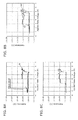
- step up if negative voltages having respective absolute values gradually increased (step up) for performing a forming (LR writing) to form a conducting path are applied at first in an initial state (approximately 25 k ⁇ ), application (point D) of a negative pulse voltage of approximately ⁇ 1.5 V (namely, a forming start voltage) causes a resistance change to a low resistance state of approximately 2.2 k ⁇ . At this time, a conducting path is formed, and a forming is performed. After that, the absolute values of the negative pulse voltages step up to approximately ⁇ 1.8 V, then gradually decreased (step down) to approximately 0 V, and then positive pulse voltages step up to be applied.
- the resistance value R is increased as the positive pulse voltages step down.
- the increase follows a path different from the pulse RV curve of the first step up.
- variable resistance nonvolatile memory element according to the present invention operates as a memory element in a bipolar region, not in a unipolar region. More specifically, the variable resistance nonvolatile memory element according to the prevent invention is a memory element that is reversibly changed between a high resistance state and a low resistance state depending on a polarity of an applied voltage pulse.
- negative pulse voltages are applied stepping up their absolute values to change a high resistance state (approximately 16 k ⁇ ) to a low resistance state.
- a negative pulse voltage of approximately ⁇ 0.7 V is applied
- the resistance state of the variable resistance nonvolatile memory device is changed to a low resistance state of approximately 3.4 k ⁇ .
- the absolute values of the negative pulse voltages step up to approximately ⁇ 1.8 V to change the resistance state to a low resistance state (approximately 1.5 k ⁇ ), then step down to approximately 0 V, and then positive pulse voltages step up to be applied.
- the same pulse RV characteristics measurement is performed as the third loop. It is seen in the third loop that, once the crest of the point E is over and pulse resistance is changed in a unipolar region, any subsequent application of a positive pulse voltage cannot achieve a significantly high level (approximately 113 k ⁇ ) of the high resistance value level, such as the point E.
- (b 1 ) to (b 3 ) in FIG. 3B have the same specimen conditions as those of (a 1 ) to (a 3 ) in FIG. 3A (refer to FIG. 2 and Table 1).
- Each of (b 1 ) to (b 3 ) in FIG. 3B shows pulse RV characteristics of another variable resistance element.
- (b 1 ) in FIG. 3B performs evaluation using the same measurement flow as that in (a 1 ) in FIG. 3A , except a difference in a maximum value of an absolute value of a negative pulse voltage (approximately 2.4 V in (b 1 ) in FIG. 3B ).
- Each of (b 2 ) and (b 3 ) in FIG. 3B performs evaluation using the same measurement flow as that in (a 1 ) in FIG. 3A .
- the second loop of the pulse RV characteristics measurement shows almost the same pulse RV characteristics as that in (a 2 ) in FIG. 3A .
- the resistance state of the variable resistance nonvolatile memory device is changed to a low resistance state of approximately 3.8 k ⁇ at a point D 3 where a negative pulse voltage of approximately ⁇ 0.6 V is applied.
- the absolute values of the negative pulse voltages step up to approximately ⁇ 1.8 V to change the resistance state to a low resistance state (approximately 1.5 k ⁇ ), then step down to approximately 0 V, and then positive pulse voltages step up to be applied.
- the positive pulse voltage of approximately 2.3 V is applied
- the low resistance state starts changing to a high resistance state (approximately 10 k ⁇ ).
- the high resistance value level becomes maximum (approximately 11 k ⁇ ).
- the positive pulse voltages step up from approximately 2.5 V to maximum approximately 5.9 V, the high resistance value level starts decreasing to a low resistance state.
- (c 1 ) to (c 3 ) in FIG. 3C have the same specimen conditions as those of (a 1 ) to (a 3 ) in FIG. 3A (refer to FIG. 2 and Table 1).
- Each of (c 1 ) to (c 3 ) in FIG. 3C shows pulse RV characteristics of still another variable resistance element.
- (c 1 ) in FIG. 3C performs evaluation using the same measurement flow as that in (b 1 ) in FIG. 3B , except a difference in a maximum value of an absolute value of a negative pulse voltage (approximately 2.8 V in (c 1 ) in FIG. 3C ).
- Each of (c 2 ) and (c 3 ) in FIG. 3C performs evaluation using the same measurement flow as that in (a 1 ) in FIG. 3A .
- (d 1 ) to (d 3 ) in FIG. 3D have the same specimen conditions as those of (a 1 ) to (a 3 ) in FIG. 3A (refer to FIG. 2 and Table 1).
- Each of (d 1 ) to (d 3 ) in FIG. 3D shows pulse RV characteristics of still another variable resistance element.
- (d 1 ) in FIG. 3D performs evaluation using the same measurement flow as that in (c 1 ) in FIG. 3C , except a difference in a maximum value of an absolute value of a negative pulse voltage (approximately 3.8 V in (d 1 ) in FIG. 3D ).
- (d 1 ) in FIG. 3D shows a difference in a maximum value of an absolute value of a negative pulse voltage (approximately 3.8 V in (d 1 ) in FIG. 3D ).
- Table 2 shows a relationship between (i) a forming margin ⁇ represented by a difference between a forming start voltage Vb (negative voltage) and an applied maximum LR writing pulse voltage VpLR (negative voltage), and (ii) a changeable maximum HR (high resistance value level).
- the experiment results show a preferable voltage to be applied in a forming for changing a variable resistance element from (i) the first state after manufacture of the variable resistance element to (ii) the second state changeable between a high resistance state and a low resistance state depending on a polarity of an applied voltage pulse.
- this preferable voltage is equal to or higher than a forming start voltage Vb that is a minimum voltage required for a change from the first state to the second state, and also is equal to or lower than a voltage (having an absolute value of 2.4V or smaller, in this example) that is obtained by adding a predetermined voltage (forming margin of 0.7V, in this example) to the forming start voltage Vb.
- a preferable voltage pulse to be applied to the variable resistance element is a voltage pulse of a voltage having an absolute value not exceeding an absolute value maximum voltage.
- the absolute value maximum voltage is a voltage obtained by adding the predetermined voltage to the forming start voltage having a minimum absolute value required to change the variable resistance element from the first state to the second state.
- (e 1 ) to (e 3 ) in FIG. 3E have the same specimen conditions as those of (a 1 ) to (a 3 ) in FIG. 3A (refer to FIG. 2 and Table 1).
- Each of (e 1 ) to (e 3 ) in FIG. 3E shows pulse RV characteristics of still another variable resistance element.
- (e 1 ) to (e 3 ) in FIG. 3E differ from (a 1 ) to (a 3 ) in FIG.
- a maximum value of a positive pulse voltage is set to approximately 2.2 V after a forming in which a negative pulse voltage up to approximately ⁇ 1.9 V is applied, so that the positive pulse voltage does not enter the unipolar region.
- relatively stable hysteresis loops are performed during the first to third loops, while keeping the high resistance value level (48 k ⁇ to 74 k ⁇ @ pulse voltage of +2.2 V) higher than that in (a 1 ) to (a 3 ) in FIG. 3A .
- pulse resistance changes using, for example, a usual HR writing pulse voltage of +2.2 V (point J) and a LR writing pulse voltage ⁇ 1.8 V (point K) result in a significantly wide operation window between a high resistance state (48 k ⁇ to 74 k ⁇ ) and a low resistance state (approximately 1.5 k ⁇ to 1.8 k ⁇ ).
- the second control rule is to control a resistance change operation after a forming not to apply a pulse voltage for HR writing (hereinafter, referred to also as a “HR writing voltage”) higher than voltages in the unipolar region (an applied voltage causing a maximum resistance value of a variable resistance element in a high resistance state).
- HR writing voltage a pulse voltage for HR writing
- both of the above two control rules are performed, it is not always necessary in the present invention to perform both of the rules. This is because performing of one of the rules is enough to generate an operation window larger than that in the case where none of the rules are performed.
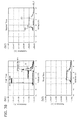
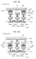
- FIGS. 6A and 6B are cross-sectional views of the 1T1R memory cell including the variable resistance element 100 shown in FIG. 5 .
- the same reference numerals of FIG. 5 are assigned to the identical structural elements of FIGS. 6A and 6B , so that the identical structural elements are not explained again below.
- a transistor 317 corresponds to the NMOS transistor shown in FIG. 5 .
- the third line layer 311 connected to the fourth via 310 corresponds to a bit line BL.
- the first line layer 305 and the second line layer 307 which are connected to the first N-type diffusion layer region 302 a of the transistor 317 correspond to a source line SL vertically arranged in FIG. 6A .
- the variable resistance element 100 has a structure in which the lower electrode 100 a , the variable resistance layer 100 b , and the upper electrode 100 c are sequentially stacked on the third via 308 to form a sandwich shape.
- the variable resistance element 100 contacts the fourth via 310 connected to the third line layer 311 .
- a memory cell structure in which an upper electrode of the variable resistance element 100 (an electrode which corresponds to 100 c in FIG. 5 and is connected to the second oxygen-deficient oxide layer ( 100 b - 2 in FIG. 5 ) having a greater oxygen content percentage and a high resistance) is connected to a bit line as shown in FIG. 6A is referred to as a I-type cell.
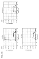
- FIG. 6B is a cross-sectional view of the second basic structure for two bits of the 1T1R memory cell.
- the third line layer 311 connected to the first N-type diffusion layer region 302 a of the transistor 317 corresponds to a bit line BL.
- the second line layer 307 connected to the second resistance film via 511 corresponds to a source line SL vertically arranged in FIG. 6B .
- a voltage of the semiconductor substrate 301 is 0 V, which is supplied from a commonly-known structure of a 0V power source line (not shown).
- the variable resistance element 100 has a structure in which the lower electrode 100 a , the variable resistance layer 100 b , and the upper electrode 100 c are sequentially stacked on the first resistance film via 510 to form a sandwich shape.
- the variable resistance element 100 contacts the second resistance film via 511 connected to the second line layer 307 .
- a word line not shown in the structures of FIGS. 6A and 6B is arranged in parallel to the source line SL, in order to apply a gate voltage to the gate electrode 303 b.
- variable resistance element 100 is as indicated in Table 1 .
- the NMOS transistor has a gate width W of 0.44 ⁇ m, a gate length L of 0.18 ⁇ m, and a gate oxide layer thickness of 3.5 nm.
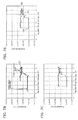
- step up negative pulse voltages having absolute values gradually increased (step up) are applied from an initial state (approximately 20 M ⁇ ) to perform a forming (LR writing as initialization) to form a conducting path. Then, at a point Z 1 where a negative pulse voltage of ⁇ 1.8 V is applied, the forming results in a low resistance state of approximately 19 k ⁇ . After the forming, the soft forming is performed by applying the negative pulse voltages stepping down not to have an absolute value higher than that of ⁇ 1.8 V.
- the situation of changing a high resistance state to a state having a resistance value less than 40 k ⁇ is defined as completion of the forming, and any negative pulse, voltage having an absolute value greater than that used in the forming is not applied after the forming.
- positive pulse voltages step up to be applied When a positive pulse voltage of approximately 1.4 V is applied, the low resistance state is changed to a high resistance state having a resistance value of approximately 31 k ⁇ . Then, at a point Z 2 where a positive pulse voltage of 2.5 V is applied, the high resistance value level becomes maximum (approximately 667 k ⁇ ). Then, when positive pulse voltages step up from 2.5 V to maximum 3.3 V (point Z 3 ), the high resistance value level starts decreasing. Subsequently, if the positive pulse voltages step down from the point Z 3 (+3.3 V), the step down follows a path different from the pulse RV curve of the first step up. After that, if the positive pulse voltages further step down to approximately 0 V, the resistance value is eventually kept in a high resistance state of approximately 333 k ⁇ .
- the high resistance value level becomes maximum (approximately 222 k ⁇ ). After that, if positive pulse voltages step up from approximately 2.2 V to maximum approximately 3.3 V, the high resistance value level becomes almost saturated. Subsequently, if the positive pulse voltages step down from a point Z 6 (+3.3 V), the resistance value follows almost the same path as that of the saturated high resistance value in the second step up. After that, when positive pulse voltages step down to approximately 0 V to be applied, the resistance value is eventually kept in a high resistance state of approximately 250 k ⁇ .
- the same pulse RV characteristics measurement is performed as the third loop.
- the third loop once the crest of the point Z 2 is over and pulse resistance change occurs between the point Z 2 and the point Z 3 (unipolar region), any subsequent application of a positive pulse voltage cannot achieve a significantly high level (approximately 667 k ⁇ ) of the high resistance value level, such as the point Z 2 .
- the high resistance value level is increased to approximately 118 k ⁇ . After that, when positive pulse voltages step down from +2.4 V, the resistance value is eventually kept in a high resistance state of approximately 133 k ⁇ .
- negative pulse voltages are applied stepping up their absolute values from the high resistance state (approximately 133 k ⁇ ) to write for low resistance.
- the resistance state is changed to a low resistance state of approximately 9.6 k ⁇ .
- the absolute values of the negative pulse voltages step up to approximately ⁇ 3.3 V, then step down to approximately 0 V, and then positive pulse voltages step up to be applied.
- a positive pulse voltage of approximately 1.7 V is applied, a low resistance state is changed to a high resistance state (approximately 60.6 k ⁇ ).
- the high resistance value level is increased to approximately 113 k ⁇ . After that, when positive pulse voltages step down from +2.4 V, the high resistance value level is slightly decreased. Then, when positive pulse voltages step down to approximately 0 V to be applied, the resistance value is eventually kept in a high resistance state of approximately 80 k ⁇ .
- the same pulse RV characteristics measurement are performed as the third loop.
- the third loop shows the same pulse RV characteristics as seen in FIG. 8B .
- the maximum value (approximately 200 k ⁇ ) of the changeable high resistance value level is lower than the high resistance value level (approximately 667 k ⁇ ) at the point Z 2 in FIG. 7A .
- FIG. 9 is a graph plotting each resistance value (resistance measurement voltage of +0.4 V) when a pulse voltage causing LR writing and a pulse voltage causing HR writing are alternately applied to the 1T1R memory cell having the pulse RV characteristics shown in FIGS. 8A to 8C .
- a horizontal axis and a vertical axis represent the same as those in FIG. 53 , and are therefore not explained again below.
- application of a pulse voltage of +2.4 V (with a pulse width of 50 ns) to the upper electrode terminal A to change a low resistance state LR of approximately 8.8 k ⁇ (here, the lower electrode side terminal C has a ground potential) in other words, application of a positive pulse voltage of +2.4 V, changes the low resistance state LR to a high resistance state HR of approximately 91 k ⁇ to 500 k ⁇ (average 261 k ⁇ ).
- FIG. 10A is a graph of measurement of pulse RV characteristics (the first loop) when the soft forming is performed.
- the pulse RV characteristics seen in FIG. 10A differ from the pulse RV characteristics seen in FIG. 8A in that negative pulse voltages are applied stepping up their absolute values to perform a forming, and when the forming (LR writing as initialization) is completed and the resistance value is changed to less than 40 k ⁇ , the absolute values of the negative pulse voltages step down from a point N not to have an absolute value higher than an absolute value of ⁇ 1.8 V (point N).
- FIGS. 10B and 10C are a graph of measurement of pulse RV characteristics when the soft forming is performed.
- FIG. 10B shows the second loop
- FIG. 10C shows the third loop.
- the pulse RV characteristics seen in FIGS. 10B and 10C differ from the pulse RV characteristics seen in FIGS. 8B and 8C in that negative pulse voltages are applied stepping up their absolute values to change a high resistance state to a low resistance state, and when the resistance value in the low resistance state reaches less than 40 k ⁇ , the absolute values of the negative pulse voltages step down from a point P not to have an absolute value greater than an absolute value of the negative pulse voltage (for example, at the point P) causing the change to less than 40 k ⁇ .
- a minimum pulse voltage (having a minimum absolute value) when a forming is performed from the initial state of the variable resistance element after its manufacture and the resistance value reaches less than 40 k ⁇ at the first time is referred to as a forming start voltage Vb.
- the high resistance value level (approximately 400 k ⁇ ) with the soft forming is controlled to have a resistance value approximately 3.4 times as high as the high resistance value level (approximately 118 k ⁇ ) without the soft forming ( FIG. 8A ). Therefore, only the first control rule is enough to obtain a larger operation window, in comparison to the case that no control rule is performed.
- FIG. 11 is a graph plotting a resistance value (a resistance measurement voltage is 0.4 V) of each application of a voltage to the 1T1R memory cell shown in FIG. 10A for which the soft forming has been performed, in the case that a pulse voltage causing LR writing and a pulse voltage causing HR writing is alternately applied.
- a horizontal axis and a vertical axis represent the same as those in FIG. 53 , and are therefore not explained again below.
- a pulse voltage applied to the variable resistance element 100 has an absolute value (1.7 V) smaller than the absolute value (1.8 V) of the forming start voltage Vb (approximately ⁇ 1.8 V). Therefore, the usual pulse change operation does not decrease the changeable high resistance value level.
- the pulse resistance change characteristics with the soft forming seen in FIG. 11 are compared to the pulse resistance change characteristics without the soft forming seen in FIG. 9 , as obvious from the results of the pulse RV characteristics, the high resistance value level (approximately 993 k ⁇ in average) of a memory cell for which the soft forming has been performed can be controlled to have a high resistance value approximately 3.8 times as high as the high resistance value level (approximately 261 ⁇ in average) of the case that the soft forming is not performed. Therefore, only the first control rule is enough to obtain a larger operation window, in comparison to the case that no control rule is performed.
- a HR writing voltage capable of setting a maximum high resistance value level is preferably from +2.4 V to +2.6 V close to the point Z in FIG. 7A . Therefore, in the experiment of the pulse VR in FIGS. 8A to 8C and 10 A to 10 C, a HR writing voltage is set to +2.4 V at maximum in order not to enter the unipolar region, thereby preventing decrease of the changeable high resistance value level. Therefore, only the second control rule is enough to obtain a larger operation window, in comparison to the case that no control rule is performed.
- the low resistance value level (approximately 9 k ⁇ to approximately 20 k ⁇ ) in the 1T1R memory cell is higher than the low resistance value level (approximately 1.5 k ⁇ to approximately 2 k ⁇ ) of the evaluation circuit in which the variable resistance element is connected in series to the fixed resistance (1 k ⁇ ) seen in (a 1 ) to (a 3 ) in FIG. 3A .
- the maximum high resistance value level in the case of performing the soft forming is higher than the low resistance value level in any cases by approximately 2 decades.
- the 1T1R memory cell for which the soft forming (the above-described first control rule) is performed can keep the high resistance value level to be higher than that of the case without the soft forming: Moreover, if pulse resistance change is occurred using a HR writing voltage not causing resistance change in the unipolar region (namely, the above-described second control rule is performed), it is possible to control the high resistance value level to be higher than the case of not performing the second control rule. Therefore, either one of these control rules is enough to enlarge an operation window between a low resistance state and a high resistance state, in comparison to the case that no control rule is performed. Although either one of the two control rules may be performed, it is preferable, of course, to perform both of them.
- FIGS. 12A and 12B are a schematic diagram of a memory cell including a variable resistance element, which explains the soft forming according to the present invention.
- a variable resistance element 600 has a structure in which a lower electrode 600 a , a variable resistance layer 600 b , and an upper electrode 600 c are sequentially stacked to form a sandwich shape.
- a lower electrode terminal E extends from the lower electrode 600 a
- an upper electrode terminal F extends from the upper electrode 600 c.
- the variable resistance layer 600 b includes a first oxygen-deficient transition metal oxide layer 600 b - 1 contacting the lower electrode 600 a , and a second oxygen-deficient transition metal oxide layer 600 b - 2 contacting the upper electrode 600 c.
- the lower electrode terminal E of the variable resistance element 600 is connected to a NMOS transistor, a Positive channel Metal Oxide Semiconductor (PMOS) transistor, or a switch element 401 made of a diode or the like.
- the other terminal of the switch element 401 which is not connected to the variable resistance element 600 extends as a lower electrode side terminal G.
- FIG. 12B is a schematic diagram of a memory cell having a structure of FIG. 12A in which a connection relationship between the variable resistance element 600 and the switch element 401 is reversed. More specifically, the upper electrode terminal F of the variable resistance element 600 is connected to the switch element 401 , and the other terminal of the switch element 401 which is not connected to the variable resistance element 600 extends as an upper electrode side terminal T.
- the lower electrode 600 a comprises tantalum nitride (TaN), tungsten (W), nickel (Ni), tantalum (Ta), titanium (Ti), and aluminium (Al).
- the upper electrode 600 c comprises platinum (Pt), iridium (Ir), palladium (Pd), silver (Ag), copper (Cu), gold (Au), and the like which are likely to occur resistance change.
- the second oxygen-deficient transition metal oxide layer 600 b - 2 has an oxygen content percentage higher than that of the first oxygen-deficient transition metal oxide layer 600 b - 1 .
- the second oxygen-deficient transition metal oxide layer 600 b - 2 has a resistance value higher than that of the first oxygen-deficient transition metal oxide layer 600 b - 1 . Since the variable resistance element 600 therefore has a high initial resistance, resistance change needs application of a forming voltage (LR writing voltage as initialization) higher than usual rewriting voltages, in order to reduce the second oxygen-deficient transition metal oxide layer 600 b - 2 to form a conducting path.
- the adoption of the memory cell structure shown in FIGS. 12A and 12B makes it possible to perform the soft forming.
- FIG. 13 is a diagram for explaining relationships among respective resistance states of a variable resistance element in a forming.
- the variable resistance element is in a high resistance state HR that is the first resistance state or in a low resistance state LR that is the second resistance state.
- the variable resistance element has an initial resistance state (resistance state of the variable resistance element for which a forming has not yet been performed) that is the third resistance state having a resistance value higher than that of the first resistance state.
- the state between the high resistance state HR and the low resistance state LR is called the fourth resistance state.
- the soft forming is performed in the following way.
- LR writing voltages in a reduction direction are applied to each memory cell a plurality of times, gradually increasing values of the LR writing voltages to change the third resistance state (initial resistance state).
- the application of the LR writing voltages is stopped not to flow excessive current to each variable resistance element.
- the soft forming is performed using a forming voltage Vb that differs depending on memory cells.
- FIG. 15 shows an initial state of a variable resistance element 100 (namely, a state where the soft forming has not yet been performed after manufacture). As shown in (b) in FIG.
- variable resistance element 100 negative voltage pulses are applied to the variable resistance element 100 , gradually increasing absolute values of the negative voltage pulses, and then when the applied negative pulse voltage VLR for LR writing reaches ⁇ V 1 , the second oxygen-deficient tantalum oxide layer 100 b - 2 as a high resistance layer is reduced by move of oxygen ion O 2 ⁇ towards the lower electrode 100 a , thereby forming a conducting path.
- the variable resistance element 100 is changed to a low resistance and thereby the soft forming has been performed.
- VLR negative pulse voltage
- the variable resistance element 100 in the state where the soft forming has been done which is shown in (b) in FIG. 15 .
- the high resistance layer the second oxygen-deficient tantalum oxide layer 100 b - 2
- the diameter of the conducting path becomes ⁇ 2 (where ⁇ 2 > ⁇ 1 ), thereby enhancing the change to a lower resistance.
- the high resistance layer (the second oxygen-deficient tantalum oxide layer 100 - b 2 ) is further reduced.
- the diameter of the conducting path becomes ⁇ 3 (where ⁇ 3 > ⁇ 2 ), thereby further enhancing the change to a lower resistance.
- the diameter of the conducting path is greater than cp 1 . Therefore, it is not possible to burry enough oxygen into the conducting path in comparison to the case that the soft forming is performed. As a result, it is estimated that the changeable high resistance value level is decreased.
- (f) in FIG. 15 shows an initial state of another variable resistance element 100 (the variable resistance element B).
- the variable resistance element 100 As shown in (g) in FIG. 15 , negative voltage pulses are applied to the variable resistance element 100 , gradually increasing absolute values of the negative voltage pulses, and then when the applied negative pulse voltage VLR for LR writing reaches ⁇ V 2 , the second oxygen-deficient tantalum oxide layer 100 b - 2 as a high resistance layer is reduced, thereby forming a conducting path. As a result, the variable resistance element 100 is changed to a low resistance and thereby the soft forming has been performed.
- the high resistance layer the second oxygen-deficient tantalum oxide layer 100 b - 2
- the diameter of the conducting path becomes ⁇ 2 (where ⁇ 2 > ⁇ 1 ), thereby enhancing the change to a lower resistance.
- the high resistance layer (the second oxygen-deficient tantalum oxide layer 100 - b 2 ) is further reduced.
- the diameter of the conducting path becomes ⁇ 3 (where ⁇ 3 > ⁇ 2 ), thereby further enhancing the change to a lower resistance.
- application of more excessive negative pulse voltage after the soft forming ((g) in FIG.
- variable resistance layer comprises an oxygen-deficient tantalum oxide as an example for explaining the mechanism of estimating the soft forming.
- the variable resistance layer may comprise an oxygen-deficient transition metal oxide for the same estimation mechanism.
- the method of writing data into the variable resistance element according to the present invention is a method of writing data into a variable resistance element changing between a high resistance state and a low resistance state depending on a polarity of an applied voltage pulse (namely, a bipolar variable resistance element).
- the writing method is mainly divided into a preparation step S 50 and a writing step S 51 (a HR writing step S 51 a and a LR writing step S 51 b ).
- each of the first voltage V 1 , the second voltage V 2 , and the third voltage V 3 is a voltage having a first polarity (positive, for example).
- the writing step S 51 is a step for storing data in an operation mode in which the variable resistance element is used as a memory element.
- the writing step S 51 includes the HR writing step S 51 a and the LR writing step S 51 b .
- a voltage pulse Vp having a first polarity (positive, for example) is applied to the variable resistance element so that the variable resistance element is changed from the low resistance state S 52 to the high resistance state S 53 .
- a voltage pulse Vn having a second polarity (negative, for example) is applied to the variable resistance element so that the variable resistance element is changed from the high resistance state S 53 to the low resistance state S 52 .
- the HR writing step S 51 a is characterized in that the applied voltage pulse has a voltage Vp having an absolute value which is equal to greater than that of the first voltage V 1 and equal to or smaller than that of the second voltage V 2 , more preferably in that the above-described voltage Vp is close to the second voltage V 2 .
- the preparation step 550 may be eliminated when the characteristics (the first voltage V 1 and the second voltage V 2 ) of the variable resistance element is already known or can be predicted.
- the absolute value may exceed that of the second voltage V 2 as long as a high resistance value can be kept in a certain range from the maximum resistance value Rmax of a high resistance state in practice.
- the range may be determined depending on a width of an operation window to be obtained. For example, if the applied voltage causes a resistance value that is 90% of the maximum resistance value Rmax, the voltage may have an absolute value exceeding that of the second voltage V 2 to achieve HR writing.
- variable resistance element being increased step by step (by 0.1 V increments, for example), so as to measure a resistance value for each application, and then a voltage causing a maximum resistance value from which the resistance value is decreased is determined as a HR writing voltage (or the second voltage V 2 ).
- a voltage equal to or lower than a voltage that is a sum of the second voltage V 2 and the above-mentioned increment voltage (0.1 V, for example) is determined as a HR writing voltage. Therefore, it is possible to determine an optimum HR writing voltage (preparation step), and perform HR writing by the determined HR writing voltage (writing step).
- a plurality of measured points are smoothed and a maximum point of the resistance values is determined from the smoothed measurement points in consideration with variations of the resistance values.
- variable resistance element used in the preparation step S 50 may be different from the variable resistance element used at the following writing step S 51 , although they are the same kind.
- the variable resistance element used in the preparation step S 50 and the variable resistance element used at the following writing step S 51 are different elements that have been manufactured under the same manufacture conditions (namely, the variable resistance element used in the preparation step S 50 is used only at the preparation step). Since the third voltage V 3 having an absolute value exceeding that of the second voltage V 2 is applied to the variable resistance element at the preparation step S 50 , the above-described unipolar characteristics do not allow any subsequent application of voltage pulse to the variable resistance element to recover the resistance value in the high resistance state to reach the maximum resistance value Rmax.
- variable resistance element used in the preparation step S 50 is different from the variable resistance element used in the writing step S 51 (here, these variable resistance elements have been manufactured under the same manufacture condition to have the same characteristics)
- application of a voltage having an absolute value not exceeding that of the second voltage V 2 obtained at the preparation step S 50 can cause the HR writing step S 51 a .
- FIG. 17 is a block diagram showing a structure of the nonvolatile memory device according to the first embodiment of the present invention.
- the nonvolatile memory device 200 includes a memory body 201 formed on a semiconductor substrate.
- the memory body 201 includes: a memory array 202 including the II-type cells shown in FIG. 6B ; a row selection circuit 208 ; a row driver 207 including word line drivers WLD (referred to also as “word line driver circuits WLD)” and source line drivers SLD (referred to also as “source line driver circuits SLD”); a column selection circuit 203 ; a writing circuit 206 for data writing; a sense amplifier 204 that detects an amount of current flowing in a selected bit line and thereby determines whether a resistance state is a high resistance state as data “0” or a low resistance state as data “1”; and a data input/output circuit 205 that receives and outputs input/output data via a terminal DQ.
- the nonvolatile memory device 200 includes a HR writing power source 213 and a LR writing power source 212 which form a writing power source 211 .
- the nonvolatile memory device 200 further includes: an address input circuit 209 that receives address signals from the outside; and a control circuit 210 that controls operations of the memory body 201 based on control signals provided from the outside.
- the memory array 202 includes a plurality of word lines WL 0 , WL 1 , WL 2 , . . . and a plurality of bit lines BL 0 , BL 1 , BL 2 , on the semiconductor substrate.
- the word lines WL 0 , WL 1 , WL 2 , . . . cross the bit lines BL 0 , BL 1 , BL 2 , respectively.
- the memory array 202 also includes a plurality of NMOS transistors N 11 , N 12 , N 13 , N 21 , N 22 , N 23 , N 31 , N 32 , N 33 , . . .
- the memory array 202 further includes a plurality of variable resistance elements R 11 , R 12 , R 13 , R 21 , R 22 , R 23 , R 31 , R 32 , R 33 , . . . (hereinafter, referred to as “variable resistance elements R 11 , R 12 , . . . .
- each of the pairs serves as a corresponding one of memory cells M 11 , M 12 , M 13 , M 21 , M 22 , M 23 , M 31 , M 32 , M 33 , . . . (hereinafter, referred to as “memory cells M 11 , M 12 , . . . ”).
- gates of the transistors N 11 , N 21 , N 31 , . . . are connected to the word line WL 0
- gates of the transistors N 12 , N 22 , N 32 , . . . are connected to the word line WL 1
- gates of the transistors N 13 , N 23 , N 33 , . . . are connected to the word line WL 2
- gates of the transistors N 14 , N 24 , N 34 , . . . are connected to the word line WL 3 .
- drains of the transistors N 11 , N 12 , N 13 , N 14 , . . . are connected to the bit line BL 0
- drains of the transistors N 21 , N 22 , N 23 , N 24 , . . . are connected to the bit line BL 1
- drains of the transistors N 31 , N 32 , N 33 , N 34 , . . . are connected to the bit line BL 2 .
- variable resistance elements R 11 , R 21 , R 31 , . . . are connected to the source line SL 0
- variable resistance elements R 12 , R 22 , R 32 , . . . are connected to the source line SL 1
- the variable resistance elements R 13 , R 23 , R 33 , . . . are connected to the source line SL 2
- the variable resistance elements R 14 , R 24 , R 34 , . . . are connected to the source line SL 3 .
- the address input circuit 209 receives address signals from an external circuit (not shown). Based on the address signals, the address input circuit 209 provides row address signals to the row selection circuit 208 and column address signals to the column selection circuit 203 .
- the address signals are signals indicating an address of a certain memory cell selected from the plurality of memory cells M 11 , M 12 , . . . .
- control circuit 210 In a data writing cycle, the control circuit 210 provides the writing circuit 206 with a write command signal instructing application of a writing voltage, based on input data Din provided to the data input/output circuit 205 . On the other hand, in a data reading cycle, the control circuit 210 provides the sense amplifier 204 with a read command signal instructing a reading operation.
- the row selection circuit 208 receives row address signals from the address input circuit 209 . Based on the row address signals, the row selection circuit 208 causes the row driver 207 to apply a predetermined voltage to a word line selected in the row address signals, by using a word line driver circuit WLD corresponding to one of the plurality of word lines WL 0 , WL 1 , WL 2 , . . . .
- the address input circuit 209 causes, based on the row address signals, the row driver 207 to apply a predetermined voltage to a source line selected in the row address signals, by using a source line driver circuit SLD corresponding to one of the plurality of source lines SL 0 , SL 1 , . . . .
- the column selection circuit 203 receives column address signals from the address input circuit 209 . Based on the column address signals, the column selection circuit 203 selects one of the plurality of bit lines BL 0 , BL 1 , BL 2 , . . . , and applies a writing voltage or a reading voltage to the selected bit line.
- the writing circuit 206 includes a usual pulse generation circuit 700 and a variable voltage pulse generation circuit 701 .
- the usual pulse generation circuit 700 is activated to apply a writing voltage (Writing voltage pulse) to the bit line selected by the column selection circuit 203 .
- the variable. voltage pulse generation circuit 701 is activated to apply a forming voltage (forming voltage pulse) to the bit line selected by the column selection circuit 203 .
- the sense amplifier 204 is an example of a reading unit which determines (detects) a resistance value of a variable resistance element in the memory cell selected by the row selection circuit 208 and the column selection circuit 203 .
- the sense amplifier 204 includes a usual determination reference circuit 702 and a forming determination reference circuit 703 .
- the usual determination reference circuit 702 has a determination level used for usual reading operations, and the forming determination reference circuit 703 has a determination level used for forming.
- the usual determination reference circuit 702 and the forming determination reference circuit 703 are controlled by a reading enable signal C 1 and a forming enable signal C 2 , respectively, provided from the control circuit 210 , so that one of the determination levels is selected to determine whether data in the selected cell is “1” or “0”.
- the determination result is provided as output data DO to an external circuit via the data input/output circuit 205 .
- the usual reading refers to determination of a resistance state (high resistance state/low resistance state) of a variable resistance element for which a forming has been performed.
- the writing power source 211 includes the HR writing power source 213 and the LR writing power source 212 .
- An output VHO of the HR writing power source 213 is provided to the row driver 207 , while an output VLO of the LR writing power source 212 is provided to the writing circuit 206 .
- FIG. 18 is a circuit diagram showing an example of a structure of the sense amplifier 204 in FIG. 17 in more detail.
- the sense amplifier 204 includes clamp transistors 219 and 220 , a reference circuit 221 , and an inverter 224 .
- the clamp transistors 219 and 220 have the same size as that of the current mirror circuit 218 having a one-to-one mirror ratio.
- the reference circuit 221 includes the usual determination reference circuit 702 and the forming determination reference circuit 703 .
- the usual determination reference circuit 702 one end of a branch in which a selection transistor 222 is connected in series to a usual reading reference resistance Rref (20 k ⁇ ) is connected to a ground potential.
- the other end of the branch is connected to a source terminal of the clamp transistor 219 .
- a gate terminal of the selection transistor 222 receives a reading enable signal C 1 . Based on the reading enable signal C 1 , the selection transistor 222 switches between a conducting state and a non-conducting state.
- the forming determination reference circuit 703 one end of a branch in which a selection transistor 223 is connected in series to a forming reference resistance Rb (90 k ⁇ ) is connected to a ground potential. The other end of the branch is connected to a source terminal of the clamp transistor 219 .
- a gate terminal of the selection transistor 223 receives a forming enable signal C 2 . Based on the forming enable signal C 2 , the selection transistor 223 switches between a conducting state and a non-conducting state.
- a gate terminal of each of the clamp transistors 219 and 220 receives a clamp voltage VCLP (0.9 V).
- a source terminal of the clamp transistor 220 is connected to the memory cells via the column selection circuit 203 and the bit lines.
- Drain terminals of the clamp transistors 219 and 220 are connected to drain terminals of transistors 225 and 226 , respectively, which are included in the current mirror circuit 218 .
- the inverter 224 performs inverting amplification to a potential of the drain terminal of the clamp transistor 220 , so as to generate a sense amplifier output SAO to be provided to the data input/output circuit 205 .
- FIG. 19 is a diagram for explaining the determination levels of the sense amplifier 204 .
- the sense amplifier 204 has two determination levels which are (a) the usual reading reference resistance Rref (20 k ⁇ ) and (b) the forming reference resistance Rb (90 k ⁇ ) greater than the usual reading reference resistance Rref, between a high resistance state HR (100 k ⁇ ) and a low resistance state LR (11 k ⁇ ).
- the forming reference resistance Rb is set to have a resistance value smaller than a resistance value of the high resistance state HR.
- the forming reference resistance Rb is set to have a resistance value smaller than a minimum possible resistance value of the variable resistance element in the high resistance state HR.
- the usual reading reference resistance Rref is set to have a resistance value that is smaller than a resistance value of the high resistance state HR and that is greater than a resistance value of the low resistance state LR.
- the usual reading reference resistance Rref is set to have a resistance value that is smaller than a minimum possible resistance value of the variable resistance element in the high resistance state HR and that is greater than a maximum possible resistance value of the variable resistance element in the low resistance state LR.
- FIG. 20 is a diagram showing an example of a structure of the writing circuit 206 in FIG. 17 in more detail.
- the writing circuit 206 includes a writing driver circuit 214 , a voltage follower circuit 215 , and a voltage-dividing circuit 216 .
- TRM 33 provided from the control circuit 210 .
- the common node NO is connected to an input terminal of the voltage follower circuit 215 .
- An output terminal VC of the voltage follower circuit 215 which outputs a potential of the common node NO is connected to the writing driver circuit 214 .
- the writing driver circuit 214 receives, as a power source, a voltage of the output terminal VC of the voltage follower circuit 215 .
- An input terminal of the writing driver circuit 214 receives a pulse application control signal from the control circuit 210 .
- An output terminal of the writing driver circuit 214 provides a writing pulse voltage Vp to the column selection circuit 203 in FIG. 17 .
- the writing voltage pulse is a voltage pulse that becomes a voltage of the output terminal VC of the voltage follower circuit 215 only in a predetermined time period (50 ns, for example) (0 V in other time periods).
- the control circuit 210 controls the voltage-dividing switch signals TRM 10 , TRM 11 , . . . , TRM 33 so as to control only a target one of the switches SW 10 to SW 33 to be ON.
- the control circuit 210 controls the voltage-dividing switch signals TRM 10 , TRM 11 , . . . , TRM 33 so as to control only a target one of the switches SW 10 to SW 33 to be ON.
- writing pulse voltages Vp which are outputs of the writing driver circuits 214 , by multiple stages depending on the pulse application control signals.
- the sense amplifier 204 is connected to a target memory cell via the column selection circuit 203 and a bit line, and the target memory cell receives a voltage not exceeding 0.4 V that is decreased from the clamp voltage VCLP (0.9 V) by a threshold voltage (0.5 V) of the clamp transistors 219 and 220 .
- the selection transistor 223 is activated by the forming enable signal C 2 to be in a conducting state, so that the forming reference resistance Rb (90 k ⁇ ) is selected.
- the clamp transistor 200 compares an amount of the load current IL to an amount of a memory cell current Ic. Based on a result of the comparison, it is detected whether a voltage of the drain terminal of the clamp transistor 220 is higher or lower than the inverted voltage (input threshold voltage) of the inverter 224 .
- the inverter 224 outputs the detection result as a sense amplifier output SAO.
- the voltage of the drain terminal of the clamp transistor 220 becomes higher than the inverted voltage of the inverter 224 after a predetermined time period. Therefore, a low (L) level is outputted as the sense amplifier output SAO.
- the sense amplifier 204 determines that the data in the memory sell is “0”, namely, failed.
- the resistance value of the selected memory cell becomes 50 k ⁇ that is smaller than the forming reference resistance Rb (90 M ⁇ )
- the load current IL approximately 4.4 ⁇ A
- the voltage of the drain terminal of the clamp transistor 220 becomes lower than the inverted voltage of the inverter 224 after a predetermined time period.
- a high (H) level is outputted as the sense amplifier output SAO.
- the sense amplifier 204 determines that the data in the memory cell is “1”, namely, passed. The determined “1” indicates that a forming has already been performed for the selected memory cell.
- the selection transistor 222 is activated by the reading enable signal C 1 to be in a conducting state, so that the usual reading reference resistance Rref is selected.
- the inverter 224 Based on a result of the comparison, it is detected whether the voltage of the drain terminal of the clamp transistor 220 is higher or lower than the inverted voltage (input threshold voltage) of the inverter 224 .
- the inverter 224 outputs the detection result as a sense amplifier output SAO.
- SAO sense amplifier output
- a L level is outputted as the sense amplifier output SAO.
- the sense amplifier 204 determines that the data in the memory sell is “0”.
- the voltage of the drain terminal of the clamp transistor 220 becomes lower than the inverted voltage of the inverter 224 . Therefore, a H level is outputted as the sense amplifier output SAO.
- the sense amplifier 204 determines that the data in the memory cell is “1”.
- a potential of the output VLO of the LR writing power source 212 is 3.3 V
- the resistance Rd 10 is 100 k ⁇
- each of the resistances Rd 11 to Rd 33 is 10 k ⁇
- a voltage amplification of the pulse application control signal is 3.3 V.
- the output terminal VC is controlled to have a voltage of 1.0 V.
- the writing driver circuits 214 can output a writing pulse voltage Vp of 1.0 V according to the pulse application control signal.
- FIG. 21 is a timing diagram of the step-up writing pulse voltage Vp which the writing circuit 206 can output.
- the switches SW 10 to SW 33 are sequentially and independently controlled to be in a conducting state. Thereby, voltages of the output terminal VC are gradually increased from 1.0 V to 3.3 V by 0.1 V increments.
- the writing pulse voltages Vp areapplied, stepping up from 1.0 V to 3.3 V by 0.1 V increments.
- FIG. 22 shows a list of various setting voltages (for a II-type cell) which are: a voltage of a word line (WL) in various operation modes including a forming, a verification reading, a LR writing, a HR writing, and a reading; a voltage of a source line (SL) (hereinafter, a SL voltage); a voltage of a bit line (BL) (hereinafter, a BL voltage); a voltage of the output VHO of the HR writing power source 213 ; and a voltage of the output VLO of the LR writing power source 212 .
- the BL voltage in a forming is the step-up writing pulse voltage Vp shown in FIG. 21
- the BL voltage in LR or HR writing is a writing pulse voltage Vp of 2.4 V amplification.
- the verification reading refers to a verification reading in a forming.
- Vp (2.4 V) is a writing pulse voltage applied from the writing circuit 206
- VL is a voltage generated in the LR writing power source 212 which is supplied to the writing circuit 206
- VH is a voltage generated in the HR writing power source 213 .
- VH is set to be a voltage (+2.4 V) at the point O in the pulse RV characteristics seen in FIG. 10A , in order not to enter the unipolar region determined by the preparation evaluation (the above-described preparation step). In short, control is performed to observe the above-described second control rule.
- a voltage of the output VHO of the HR writing power source 213 is applied to the source lines with reference to the bit lines, it is also possible to set the voltage to be relatively high so that a maximum voltage of the source lines is effectively within a range not exceeding the voltage (+2.4 V) of the point 0 , in consideration of decrease of the voltage due to parasitic resistance occurred between the HR writing power source 213 and the source lines.
- VH is set to be 2.4 V likewise in HR writing
- Vp (2.4 V) is a writing pulse voltage occurred in the writing circuit 206 .
- Vp is a writing pulse voltage that exceeds the point P and does not exceed the point N in the pulse RV properties seen in FIGS. 10A and 10B , and is effectively applied to the memory cells M 11 , M 12 , . . . .
- Vp is a step-up writing pulse voltage applied from the writing circuit 206
- VH is a voltage generated in the HR writing power source 213 .
- VH is set to be 3.3 V so that a writing pulse voltage Vp having a high voltage can be applied in the forming.
- Vread is a reading voltage (0.4 V) clamped by the sense amplifier 204 .
- Vread is in a negative voltage direction in the pulse RV properties seen in FIGS. 10A to 10C , thereby corresponding to a voltage value ( ⁇ 0.4 V) adjusted not to disturb the reading (namely, not to change a resistance state of a target variable resistance element).
- VDD corresponds to a voltage of the power supplied to the nonvolatile memory device 200 .
- the description is given for an example of the soft forming for the variable resistance nonvolatile memory device with reference to a flowchart of the soft forming in FIG. 23 .
- the LR writing pulse voltage Vp is set to 1.0 V (S 31 : the first step). Then, it is determined whether or not the writing pulse voltage Vp is equal to or lower than 3.3 V (S 32 : the second step). If the writing pulse voltage Vp is higher than 3.3 V (No at the second step), then the soft forming operation is terminated as being a failure.
- AD it is determined whether or not the address AD of the selected memory cell M 11 is equal to or smaller than a final address ADf in the memory array 202 (S 34 : the fourth step). If the address AD is equal to or smaller than the final address ADf (Yes at the fourth step), then a verification reading is performed to verify whether or not a resistance value Rc of the selected memory cell is smaller than a reference resistance Rb (Rc ⁇ Rb) (S 35 : the fifth step (determination step)).
- the resistance value Rc of the selected memory cell is smaller than the forming reference resistance Rb (Rc ⁇ Rb) (Yes at the fifth step), then it is determined that the resistance value has been decreased enough not to require a forming, thereby the address AD of the selected memory cell is incremented (S 37 : the seventh step), and a memory cell having a next address AD is selected.
- the set writing pulse voltage Vp is used to apply a negative voltage pulse ( ⁇ 1.0 V with a pulse width of 50 ns) for performing a forming to write (“1”) to the selected memory cell (S 36 : the sixth step (voltage application step).
- the address AD of the selected memory cell is incremented (S 37 : the seventh step), and a memory cell having a next address AD is selected.
- the processing from the fourth step (S 34 ) to the seventh step (S 37 ) is repeated until the address AD of the selected memory cell becomes greater than the final address ADf.
- an external device such as a memory tester determines whether or not each of resistance values Rc of all memory cells in the memory array 202 is smaller than the forming reference resistance Rb (Rc ⁇ Rb) (S 38 : the eighth step). If all of the resistance values Rc are not smaller than the forming reference resistance Rb (No at the eighth step), then the writing pulse voltage Vp is incremented by +0.1 V to be +1.1 V (S 39 : the night step). Next, It is determined whether or not the writing pulse voltage Vp is equal to or less than 3.3 V (S 32 : the second step).
- the flow of the forming includes: (a) the determination step S 35 to determine whether or not a resistance value of the variable resistance element 100 is smaller than a resistance value in a high resistance state; and (b) the voltage application step S 36 to apply a voltage pulse not exceeding a sum of a forming voltage and a forming margin (0.7 V) when the determination step S 35 determines that the resistance value of the variable resistance element 100 is smaller than the resistance value in a high resistance state (No at S 35 ).
- the determination step S 35 and the voltage application step S 36 are repeated to process all memory cells in the memory array 202 (S 34 to S 37 ).
- the voltage is increased by 0.1 V that does not exceed the forming margin (0.7 V).
- the determination step S 35 and the voltage application step S 36 are repeated to process all memory cells (S 34 to S 37 ).
- an applied forming voltage is increased by voltage (0.1 V) increment that is lower than the forming margin (0.7 V) for the soft forming.
- the soft forming can be achieved using an appropriate forming voltage Vb for each of the memory cells M 11 , M 12 , . . .
- the soft forming shown in FIG. 23 it is possible to apply a writing pulse voltage Vp only to memory cells requiring the forming, and also possible to minimize the voltage switch (increment) operations for the writing pulse voltage Vp. As a result, the soft forming can be performed at a high speed for the memory array.
- the writing pulse voltage Vp for performing a forming is incremented by +0.1 V (the ninth step), but, in the present invention, the writing pulse voltage Vp may be incremented not only by the increment voltage (0.1 V) but also by a voltage that is smaller than the forming margin (here, 0.7 V).
- a minimum voltage for a sum of a forming and the forming margin is a maximum voltage (an example of a voltage having a maximum absolute value)
- a writing voltage pulse for a forming is applied to surely perform the soft forming.
- variable resistance nonvolatile memory device Examples of the operations in a data writing cycle, a reading cycle, and the soft forming for the variable resistance nonvolatile memory device having the above-described structure are described with reference to timing diagrams shown in FIGS. 24A to 24C and 25 , the block diagram of the variable resistance nonvolatile memory device according to the first embodiment of the present invention in FIG. 17 , and the graphs for explaining the pulse RV properties in FIGS. 10A to 10C .
- FIGS. 24A to 24C are timing diagrams of operation examples performed by the nonvolatile memory device according to the first embodiment of the present invention.
- data is “0” when the variable resistance layer is in a high resistance state, and that data is “1” when the variable resistance layer is in a low resistance state.
- the description is given only for the situation that data is written to and read from the memory cell M 11 .
- the selected bit line BL 0 is set to have a voltage VH (2.4 V) and the selected source line SL 0 is'set to have a voltage Vp (2.4 V).
- the selected word line WL 0 is set to have a voltage VH (2.4 V).
- the NMOS transistor N 11 in the selected memory cell M 11 in FIG. 17 is still OFF.
- the voltage of 2.4 V is applied to both the drain and source terminals of the NMOS transistor N 11 in FIG. 17 . Therefore, current does not flow regardless of ON/OFF of the transistor.
- the selected bit line BL 0 is set to have a voltage of 0 V in a predetermined time period.
- a pulse waveform is applied to cause the selected bit line BL 0 to have the voltage Vp (2.4 V) again.
- a positive pulse voltage (+2.4 V) at the point O in the pulse RV characteristics seen in FIG. 10A is applied to the memory cell M 11 in FIG. 17 . Therefore, writing performs to change a low resistance value to a high resistance value.
- the word line WL 0 is set to have a voltage of 0 V. As a result, data “0” has been written in the memory cell M 11 .
- a memory cell is selected in a row direction by the source line and the word line, and then a pulse waveform in a negative voltage direction is applied to a certain bit line, so that a positive voltage pulse is applied to a variable resistance element in the memory cell selected by the source line, the word line, and the bit line, thereby achieving HR writing.
- the selected bit line BL 0 and the selected source line SL 0 are set to have a voltage of 0 V.
- the selected word line WL 0 is set to have a voltage VH (2.4 V), thereby turning ON the NMOS transistor N 11 of the selected memory cell M 11 in FIG. 17 .
- the selected bit line BL 0 is set to have a voltage Vp (2.4 V) in a predetermined time period.
- a pulse waveform is applied to cause the selected bit line BL 0 to have a voltage of 0 V again.
- a negative pulse voltage that exceeds the point P and does not exceed the point N in the pulse RV properties shown in FIGS. 10A and 10B is applied to the memory cell M 11 in FIG. 17 . Therefore, writing performs to change a high resistance value to a low resistance value.
- the word line WL 0 is set to have a voltage of 0 V. As a result, data “1” has been written in the memory cell M 11 .
- a memory cell is selected in a row direction by the source line and the word line, and then a pulse waveform in a positive voltage direction is applied to a certain bit line, so that a negative voltage pulse is applied to a variable resistance element in the memory cell selected by the source line, the word line, and the bit line, thereby achieving LR writing.
- the present invention is not limited to the above method.
- the selected bit line BL 0 and the selected source line SL 0 are set to have a voltage of 0 V.
- the selected word line WL 0 is set to have a voltage VDD (1.8 V), thereby turning ON the NMOS transistor N 11 of the selected memory cell M 11 .
- the selected bit line BL 0 is set to have the reading voltage Vread of 0.4 V in a predetermined time period, and the sense amplifier 204 detects a value of the current flowing in the selected memory cell M 11 to determine whether the data stored in the selected memory cell M 11 is data “0” or data “1”.
- the word line WL 0 is set to have a voltage of 0 V. As a result, the data reading operation is completed.
- FIG. 25 is a timing diagram of the soft forming operation performed by the nonvolatile memory device according to the first embodiment of the present invention.
- the soft forming operation soft forming
- FIG. 25 by accessing only one bit of the memory cell M 11 having the address AD of 0, the flow of the soft forming shown in FIG. 23 is achieved for the bit, not for the array (however, the fourth and seventh steps are eliminated because of the one-bit access).
- each voltage of the word line WL 0 , the bit line BL 0 , and the source line SL 0 of the target memory cell M 11 is 0 V.
- the memory cell M 11 is in an initial state.
- the writing pulse voltage Vp is equal to or lower than 3.3 V.
- the selected word line WL 0 is set to have a voltage VDD (1.8 V), thereby turning ON the NMOS transistor N 11 in the selected memory cell M 11 .
- the selected bit line BL 0 is set to have the reading voltage Vread of 0.4 V in a predetermined time period, and the sense amplifier 204 detects a value of the current flowing in the selected memory cell M 11 to determine whether or not the reference value Rc of the selected memory cell M 11 is smaller than the forming reference resistance Rb (Rc ⁇ Rb).
- the sense amplifier output (terminal) SAO outputs a L level, provides data “0” to the terminal DQ, and informs the external device (a memory tester, for example) of that the forming fails (false).
- each of the word line WL 0 and the bit line BL 0 is set to have a voltage of 0 V, and the verification reading operation is completed.
- each voltage of the selected bit line BL 0 , source line SL 0 , and word line WL 0 is set to be 0 V.
- the selected word line WL 0 is set to have a voltage VH (3.3 V), thereby turning ON the NMOS transistor N 11 of the selected memory cell M 11 in FIG. 17 .
- the selected bit line BL 0 is set to have a voltage Vp (1.0 V) in a predetermined time period.
- a pulse waveform negative voltage pulse
- a negative pulse voltage higher namely, having an absolute value smaller than that of
- the selected memory cell M 11 is still in the initial state and a forming is not performed for the selected memory cell M 11 .
- the forming fails.
- the word line WL 0 is set to have a voltage of 0 V.
- the forming LR writing is completed.
- the determination at the fifth step is made that the forming fails (false), and therefore the processing proceeds to the ninth step.
- the writing pulse voltage Vp is equal to or lower than 3.3 V.
- the verification reading operation (Rc ⁇ Rb or not) is performed in the same manner as the fifth step in the first loop.
- the sense amplifier output (terminal) SAO outputs a L level, provides data “0” to the terminal DQ, and informs the external device (a memory tester, for example) of that a forming fails (false).
- the verification reading operation is completed.
- each voltage of the selected bit line BL 0 , source line SL 0 , and word line WL 0 is set to be 0 V.
- the selected word line WL 0 is set to have a voltage VH (3.3 V), thereby turning ON the NMOS transistor N 11 of the selected memory cell M 11 in FIG. 17 .
- the selected bit line BL 0 is set to have a voltage Vp (1.1 V) in a predetermined time period.
- a pulse waveform (negative voltage pulse) is applied to cause the selected bit line BL 0 to have a voltage of 0 V again.
- a negative pulse voltage higher namely, having an absolute value smaller than that of
- the forming fails.
- the word line WL 0 is set to have a voltage of 0 V.
- the forming LR writing in the second loop is completed.
- the loop from the second step to the ninth step (except the fourth and seventh steps) in FIG. 23 , namely, a set of the verification reading operation and the forming LR writing operation, is repeated from three to eight times (loops).
- the resistance value Rc of the memory cell M 11 is still in the initial state and is equal to or greater than the forming reference resistance Rb. In short, the forming fails.
- the writing pulse voltage Vp is equal to or lower than 3.3 V.
- the verification reading operation (Rc ⁇ Rb or not) is performed.
- the sense amplifier output (terminal) SAO outputs a L level, provides data “0” to the terminal DQ, and informs the external device (a memory tester, for example) of that a forming fails (false).
- the verification reading operation is completed.
- each voltage of the selected bit line BL 0 , source line SL 0 , and word line WL 0 is set to be 0 V.
- the selected word line WL 0 is set to have a voltage VH (3.3 V), thereby turning ON the NMOS transistor N 11 of the selected memory cell M 11 in FIG. 17 .
- the selected bit line BL 0 is set to have a voltage Vp (1.8 V) in a predetermined time period.
- a pulse waveform (negative voltage pulse) is applied to cause the selected bit line BL 0 to have a voltage of 0 V again.
- a conducting path is formed from the initial high resistance state, so that the resistance value is changed to a resistance value after the forming that is between the high resistance state HR and the low resistance state LR.
- a forming is performed.
- the forming is success at the first time.
- the word line WL 0 is set to have a voltage of 0 V.
- the forming LR writing in the ninth loop is completed.
- the determination at the fifth step before the forming LR writing is made that the forming fails (false), and therefore the processing proceeds to the ninth step.
- the writing pulse voltage Vp is equal to or lower than 3.3 V.
- the verification reading operation (Rc ⁇ Rb ?) is performed.
- the sense amplifier output (terminal) SAO outputs a H level, provides data “1” to the terminal DQ, and informs the external device (a memory tester, for example) of that a forming is successful (true).
- the verification reading operation is completed.
- negative voltage pulses are applied, gradually increasing its absolute value by 0.1 V increments. For each application, completion of a forming is examined. Thereby, a negative voltage pulse equal to or higher than the above voltage is not applied after the completion of the forming. As a result, after a forming using a predetermined writing pulse voltage Vp, any excessive pulse voltage is not applied to the memory cell M 11 .
- each of a HR writing pulse voltage and a LR writing pulse voltage is set to be 2.4 V, and their pulse widths are set to be 50 ns. Thereby, a usual data “0” writing (HR writing) and a usual data “1” writing (LR writing) are possible.
- the soft forming is performed for each memory cell (in other words, the above-described first control rule is observed).
- the changeable high resistance value level can be controlled to be higher.
- a HR writing voltage near a maximal point which is not in the unipolar region is used to perform HR writing (in other words, the above-described second control rule is observed).
- the high resistance value level can be set to be possible maximum (see FIGS. 10A to 10C and 11 ).
- a high-speed reading and data reliability can be improved, and a risk of erroneous reading can be significantly reduced.
- the LR writing voltage for data “1” writing is, of course, set not to decrease the changeable high resistance value level due to the forming margin ⁇ greater than 0.7 V.
- FIG. 26 is a block diagram showing a structure of the nonvolatile memory device according to the second embodiment of the present invention.
- FIG. 17 The same reference numerals of FIG. 17 are assigned to the identical structural elements of FIG. 26 , so that the identical structural elements are not explained again below.
- the nonvolatile memory device 227 shown in FIG. 26 differs from the nonvolatile memory device 200 according to the first embodiment in that the memory array 202 is replaced by a memory array 229 including the I-type cells shown in FIG. 6A , that the writing circuit 206 is replaced by a writing circuit 230 , and that the row driver 207 is replaced by a row driver 231 .
- the memory body 228 includes: the memory array 229 ; the row selection circuit 208 ; the row driver 231 including the word line drivers WLD, the source line drivers SLD, and a variable voltage pulse generation circuit 704 ; the column selection circuit 203 ; the writing circuit 230 for data writing; the sense amplifier 204 that detects an amount of current flowing in a selected bit line and thereby determines whether a resistance state is a high resistance state as data “0” or a low resistance state as data “1”; and the data input/output circuit 205 that receives and outputs input/output data via the terminal DQ.
- the memory array 229 includes the plurality of word lines WL 0 , WL 1 , WL 2 , . . . and the plurality of bit lines BL 0 , BL 1 , BL 2 , . . . , on the semiconductor substrate.
- the word lines WL 0 , WL 1 , WL 2 , . . . cross the bit lines BL 0 , BL 1 , BL 2 , . . . , respectively.
- the memory array 229 also includes the plurality of NMOS transistors N 11 , N 12 , N 13 , N 21 , N 22 , N 23 , N 31 , N 32 , N 33 , . . .
- the memory array 229 further includes the plurality of variable resistance elements R 11 , R 12 , R 13 , R 21 , R 22 , R 23 , R 31 , R 32 , R 33 , . . . (hereinafter, referred to as “variable resistance elements R 11 , R 12 , . . . .
- each of the pairs serves as a corresponding one of the memory cells M 11 , M 12 , M 13 , M 21 , M 22 , M 23 , M 31 , M 32 , M 33 , . . . (hereinafter, referred to as “memory cells M 11 , M 12 , . . . ”).
- gates of the transistors N 11 , N 21 , N 31 , . . . are connected to the word line WL 0
- gates of the transistors N 12 , N 22 , N 32 , . . . are connected to the word line WL 1
- gates of the transistors N 13 , N 23 , N 33 , . . . are connected to the word line WL 2
- gates of the transistors N 14 , N 24 , N 34 , . . . are connected to the word line WL 3 .
- the transistors N 11 , N 21 , N 31 , . . . and the transistors N 12 , N 22 , N 32 , . . . are connected to the same source line SL 0 .
- the transistors N 13 , N 23 , N 33 , . . . and the transistors N 14 , N 24 , N 34 are connected to the same source line SL 2 .
- variable resistance elements R 11 , R 12 , R 13 , R 14 , . . . are connected to the same bit line BL 0
- the variable resistance elements R 21 , R 22 , R 23 , R 24 , . . . are connected to the same bit line BL 1
- the variable resistance elements R 31 , R 32 , R 33 , R 34 , . . . are connected to the same bit line BL 2 .
- the memory array 229 according to the second embodiment has a structure (I-type cell structure) in which each of the variable resistance elements R 11 , R 12 , R 13 , . . . is connected directly to a corresponding one of the bit lines BL 0 , BL 1 , BL 2 , . . . not through the NMOS transistors N 11 , N 12 , . . . .
- control circuit 210 In a data writing cycle, the control circuit 210 provides the writing circuit 230 with a write command signal instructing application of a writing voltage, based on input data Din provided to the data input/output circuit 205 . On the other hand, in a data reading cycle, the control circuit 210 provides the sense amplifier 204 with a read command signal instructing a reading operation.
- the row selection circuit 208 receives row address signals from the address input circuit 209 . Based on the row address signals, the row selection circuit 208 causes the row driver 231 to apply a predetermined voltage to a word line selected in the row address signals, by using a word line driver circuit WLD corresponding to one of the plurality of word lines WL 0 , WL 1 , WL 2 , . . . .
- the address input circuit 209 causes, based on the row address signals, the row driver 231 to apply a predetermined voltage generated by the variable voltage pulse generation circuit 704 to a source line selected in the row address signals, by using a source line driver circuit SLD corresponding to one of the plurality of source lines SL 0 , SL 2 , . . . .
- the writing circuit 230 In receiving a write command signal from the control circuit 210 , the writing circuit 230 applies a writing voltage (writing voltage pulse Vp) to the bit line selected by the column selection circuit 203 .
- the writing power source 211 includes the LR writing power source 212 and the HR writing power source 213 .
- the output VLO of the LR writing power source 212 is provided to the row driver 231 , while the output VHO of the HR writing power source 213 is provided to the writing circuit 230 .
- FIG. 27 is a diagram showing an example of the structure of the variable voltage generation circuit 704 shown in FIG. 26 .
- the same reference numerals of FIG. 20 are assigned to the identical structural elements of FIG. 27 , so that the identical structural elements are not explained again below.
- the output terminal VC of the voltage follower circuit 215 is connected to respective power source terminals of the source line driver circuits SLD. Therefore, regarding the source line driver control signals, the following is possible.
- the control circuit 210 controls the voltage-dividing switch signals TRM 10 , TRM 11 , . . . , TRM 33 so as to control only a target one of the switches SW 10 to SW 33 to be ON.
- variable voltage pulse generation circuit 704 At first, an operation performed by the variable voltage pulse generation circuit 704 is described.
- a potential of the output VLO of the LR writing power source 212 is 3.3 V
- the resistance Rd 10 is 100 k ⁇
- each of the resistances Rd 11 to Rd 33 is 10 k ⁇
- a voltage amplification of the pulse application control signal is 3.3 V.
- the output terminal VC is controlled to have a voltage of 1.0 V.
- the source line driver circuits SLD can output a writing pulse voltage Vp of 1.0 V according to the source line driver control signal.
- FIG. 28 is a timing diagram of a step-up writing pulse voltage Vp which the source line driver circuits SLD can output.
- the switches SW 10 to SW 33 are sequentially and independently controlled to be in a conducting state. Thereby, voltages of the output terminal VC are gradually increased from 1.0 V to 3.3 V by 0.1 V increments.
- the writing pulse voltages Vp are applied, stepping up from 1.0 V to 3.3 V by 0.1 V increments.
- FIG. 29 shows a list of various setting voltages (for a I-type cell) which are: a voltage of a word line (WL) in various operation modes including a forming, a verification reading, a LR writing, a HR writing, and a reading; a voltage of a source line (SL) (hereinafter, a SL voltage); a voltage of a bit line (BL) (hereinafter, a BL voltage); a voltage of the output VHO of the HR writing power source 213 ; and a voltage of the output VLO of the LR writing power source 212 .
- the SL voltage in a forming is the step-up writing pulse voltage Vp shown in FIG.
- the BL voltage in LR or HR writing is a pulse voltage of 2.4 V amplification.
- VL is a voltage generated in the LR writing power source 212
- Vp (2.4 V) is a writing pulse voltage applied from the source line driver circuit SLD
- VH is a voltage generated in the HR power source 213 to be supplied to the writing circuit 230 .
- Vp is a writing pulse voltage that exceeds the point P and does not exceed the point N in the pulse RV properties seen in FIGS. 10A and 10B , and is effectively applied to the memory cells M 11 , M 12 , . . . .
- VL is a voltage generated in the LR writing power source 212
- VH is a voltage generated in the HR writing power source 213 to be supplied to the writing circuit 230 .
- VH is set to be a voltage (+2.4 V) at the point O in the pulse RV characteristics seen in FIG. 10A , in order not to enter the unipolar region determined by the preparation evaluation. In short, control is performed to observe the above-described second control rule.
- a voltage of the output VHO of the HR writing power source 213 is applied to the source lines with reference to the bit lines, it is also possible to set the voltage to be relatively high so that a maximum voltage of the source lines is effectively within a range not exceeding the voltage (+2.4 V) of the point O, in consideration of decrease of the voltage due to parasitic resistance occurred between the HR writing power source 213 and the source lines.
- Vp is a step-up writing pulse voltage applied from the source line driver circuit SLD
- VL is a voltage generated in the LR writing power source 212 .
- VL is set to be 3.3 V so that a writing pulse voltage Vp having a high voltage can be applied in the forming.
- Vread is a reading voltage (0.4 V) clamped by the sense amplifier 204 .
- Vread is in a positive voltage direction in the pulse RV properties seen in FIGS. 10A to 10C , thereby corresponding to a voltage value (+0.4 V) adjusted not to disturb the reading (namely, not to change a resistance state of a target variable resistance element).
- VDD corresponds to a voltage of the power supplied to the nonvolatile memory device 227 .
- FIGS. 30A to 30C are timing diagrams of operation examples performed by the nonvolatile memory device according to the second embodiment of the present invention.
- data is “0” when the variable resistance layer is in a high resistance state
- data is “1” when the variable resistance layer is in a low resistance state.
- the description is given only for the situation that data is written to and read from the memory cell M 11 .
- the selected bit line BL 0 is set to have a voltage VH (2.4 V) and the selected source line SL 0 is set to have a voltage Vp (2.4 V).
- the selected word line WL 0 is set to have a voltage VL (2.4 V).
- the NMOS transistor Nil in the selected memory cell M 11 in FIG. 26 is still OFF.
- the voltage of 2.4 V is applied to both the drain and source terminals of the NMOS transistor N 11 in FIG. 26 . Therefore, current does not flow regardless of ON/OFF of the transistor.
- the selected bit line BL 0 is set to have a voltage of 0 V in a predetermined time period.
- a pulse waveform is applied to cause the selected bit line BL 0 to have the voltage VH (2.4 V) again.
- a negative pulse voltage that exceeds the point P and does not exceed the point N in the pulse RV properties shown in FIGS. 10A and 10B is applied to the memory cell M 11 in FIG. 26 . Therefore, writing performs to change a high resistance value to a low resistance value.
- the word line WL 0 is set to have a voltage of 0 V. As a result, data “1” has been written in the memory cell M 11 .
- a memory cell is selected in a row direction by the source line and the word line, and then a pulse waveform in a negative voltage direction is applied to a certain bit line, so that a negative voltage pulse is applied to a variable resistance element in the memory cell selected by the source line, the word line, and the bit line, thereby achieving LR writing.
- the selected bit line BL 0 and the selected source line SL 0 are set to have a voltage of 0 V.
- the selected word line WL 0 is set to have a voltage VL (2.4 V), thereby turning ON the NMOS transistor N 11 of the selected memory cell M 11 in FIG. 26 .
- the selected bit line BL 0 is set to have the voltage VH (2.4 V) in a predetermined time period.
- a pulse waveform is applied to cause the selected bit line BL 0 to have 0 V again.
- a positive pulse voltage (+2.4 V) at the point O in the pulse RV characteristics seen in FIG. 10A is applied to the memory cell M 11 in FIG. 26 . Therefore, writing performs to change a low resistance value to a high resistance value.
- the word line WL 0 is set to have a voltage of 0 V. As a result, data “0” has been written in the memory cell M 11 .
- a memory cell is selected in a row direction by the source line and the word line, and then a pulse waveform in a positive voltage direction is applied to a certain bit line, so that a positive voltage pulse is applied to a variable resistance element in the memory cell selected by the source line, the word line, and the bit line, thereby achieving HR writing.
- the selected bit line BL 0 and the selected source line SL 0 are set to have a voltage of 0 V.
- the selected word line WL 0 is set to have a voltage VDD (1.8 V), thereby turning ON the NMOS transistor N 11 of the selected memory cell M 11 .
- the selected bit line BL 0 is set to have the reading voltage Vread of 0.4 V in a predetermined time period, and the sense amplifier 204 detects a value of the current flowing in the selected memory cell M 11 to determine whether the data stored in the selected memory cell M 11 is data “0” or data “1”.
- the word line WL 0 is set to have a voltage of 0 V. As a result, the data reading operation is completed.
- FIG. 31 is a timing diagram of the soft forming operation performed by the nonvolatile memory device according to the second embodiment of the present invention.
- the soft forming operation shown in FIG. 31 by accessing only one bit of the memory cell M 11 having the address AD of 0, the flow of the soft forming shown in FIG. 23 is achieved for the bit, not for the array (however, the fourth and seventh steps are eliminated because of the one-bit access).
- each voltage of the word line WL 0 , the bit line BL 0 , and the source line SL 0 of the target memory cell M 11 is 0 V.
- Each of the voltage-dividing switch signals TRM 10 , TRM 11 , TRMmn (where m is an integer from 1 to 3, and n is an integer from 0 to 9) and the terminal DQ is a L level.
- the do memory cell M 11 is in an initial state.
- the writing pulse voltage Vp is equal to or lower than 3.3 V.
- the selected word line WL 0 is set to have a voltage VDD (1.8 V), thereby turning ON the NMOS transistor N 11 in the selected memory cell M 11 .
- the selected bit line BL 0 is set to have the reading voltage Vread of 0.4 V in a predetermined time period, and the sense amplifier 204 detects a value of the current flowing in the selected memory cell M 11 to determine whether or not the reference value Rc of the selected memory cell M 11 is smaller than the forming reference resistance Rb (Rc ⁇ Rb).
- the sense amplifier output (terminal) SAO outputs a L level, provides data “0” to the terminal DQ, and informs the external device (a memory tester, for example) of that the forming fails (false).
- each of the word line WL 0 and the bit line BL 0 is set to have a voltage of 0 V, and the verification reading operation is completed.
- each voltage of the selected bit line BL 0 , source line SL 0 , and word line WL 0 is set to be 0 V.
- the selected word line WL 0 is set to have a voltage VL (3.3 V), thereby turning ON the NMOS transistor N 11 of the selected memory cell M 11 in FIG. 26 .
- the selected source line SL 0 is set to have a voltage Vp (1.0 V) in a predetermined time period.
- a pulse waveform (a negative voltage pulse for the source line) is applied to cause the selected source line SL 0 to have a voltage of 0 V again.
- a negative pulse voltage higher namely, having an absolute value smaller than that of
- the forming fails.
- the word line WL 0 is set to have a voltage of 0 V.
- the forming LR writing is completed.
- the determination at the fifth step is made that the forming fails (false), and therefore the processing proceeds to the ninth step.
- the writing pulse voltage Vp is equal to or lower than 3.3 V.
- the verification reading operation (Rc ⁇ Rb or not) is performed in the same manner as the fifth step in the first loop.
- the sense amplifier output (terminal) SAO outputs a L level, provides data “0” to the terminal DQ, and informs the external device (a memory tester, for example) of that a forming fails (false).
- the verification reading operation is completed.
- each voltage of the selected bit line BL 0 , source line SL 0 , and word line WL 0 is set to be 0 V.
- the selected word line WL 0 is set to have a voltage VL (3.3 V), thereby turning ON the NMOS transistor N 11 of the selected memory cell M 11 in FIG. 26 .
- the selected source line SL 0 is set to have a voltage Vp (1.1 V) in a predetermined time period.
- a pulse waveform (negative voltage pulse) is applied to cause the selected source line SL 0 to have a voltage of 0 V again.
- a negative pulse voltage higher namely, having an absolute value smaller than that of
- the forming fails.
- the word line WL 0 is set to have a voltage of 0 V.
- the forming LR writing in the second loop is completed.
- the loop from the second step to the ninth step (except the fourth and seventh steps) in FIG. 23 , namely, a set of the verification reading operation and the forming LR writing operation, is repeated from three to eight times (loops).
- the resistance value Rc of the memory cell M 11 is still in the initial state and is equal to or greater than the forming reference resistance Rb. In short, the forming fails.
- the writing pulse voltage Vp is equal to or lower than 3.3 V.
- the verification reading operation (Rc ⁇ Rb or not) is performed.
- the sense amplifier output (terminal) SAO outputs a L level, provides data “0” to the terminal DQ, and informs the external device (a memory tester, for example) of that a forming fails (false).
- the verification reading operation is completed.
- each voltage of the selected bit line BL 0 , source line SL 0 , and word line WL 0 is set to be 0 V.
- the selected word line WL 0 is set to have a voltage VL (3.3 V), thereby turning ON the NMOS transistor N 11 of the selected memory cell M 11 in FIG. 26 .
- the selected source line SL 0 is set to have a voltage Vp (1.8 V) in a predetermined time period.
- the determination at the fifth step before the forming LR writing is made that the forming fails (false), and therefore the processing proceeds to the ninth step.
- the writing pulse voltage Vp is equal to or lower than 3.3 V.
- the verification reading operation (Rc ⁇ Rb or not) is performed.
- the sense amplifier output (terminal) SAO outputs a H level, provides data “1” to the terminal DQ, and informs the external device (a memory tester, for example) of that a forming is successful (true).
- the verification reading operation is completed.
- negative voltage pulses are applied, gradually increasing their absolute value by 0.1 V increments. For each application, completion of a forming is examined. Thereby, a negative voltage pulse equal to or higher than the above voltage is not applied after the completion of the forming. As a result, after a forming using a predetermined writing pulse voltage Vp, any excessive pulse voltage is not applied to the memory cell M 11 .
- each of a HR writing pulse voltage and a LR writing pulse voltage is set to be 2.4 V, and their pulse widths are set to be 50 ns. Thereby, a usual data “0” writing (HR writing) and a usual data “1” writing (LR writing) are possible.
- the LR writing voltage for data “1” writing is, of course, set not to decrease the changeable high resistance value level due to the forming margin LI greater than 0.7 V.
- FIG. 32 is a block diagram showing a structure of the nonvolatile memory device according to the third embodiment of the present invention.
- FIG. 26 The same reference numerals of FIG. 26 are assigned to the identical structural elements of FIG. 32 , so that the identical structural elements are not explained again below.
- control circuit 210 In a data writing cycle, the control circuit 210 provides the writing circuit 271 with a write command signal instructing application of a writing voltage, based on input data Din provided to the data input/output circuit 205 . On the other hand, in a data reading cycle, the control circuit 210 provides the sense amplifier 204 with a read command signal instructing a reading operation.
- the row selection circuit 208 receives row address signals from the address input circuit 209 . Based on the row address signals, the row selection circuit 208 causes the row driver 273 to apply a predetermined voltage to a word line selected in the row address signals, by using a word line driver circuit WLD corresponding to one of the plurality of word lines WL 0 , WL 1 , WL 2 , . . . .
- the address input circuit 209 causes, based on the row address signals, the row driver 273 to apply a predetermined voltage to a source line selected in the row address signals, by using a source line driver circuit SLD corresponding to one of the plurality of source lines SL 0 , SL 2 , . . . .
- the writing circuit 271 In receiving a write command signal from the control circuit 210 , the writing circuit 271 applies a writing voltage to the bit line selected by the column selection circuit 203 .
- the writing power source 211 includes the LR writing power source 212 and the HR writing power source 213 .
- the output VLO of the LR writing power source 212 is provided to the row driver 273 , while the output VHO of the HR writing power source 213 is provided to the writing circuit 271 .
- the voltage-dividing circuit 233 33 fixed resistances Rd 1 to Rd 33 are connected in series to one another, between a voltage VH outputted from the HR writing power source 213 and a ground potential.
- Each of the switches SW 1 to SW 33 can be independently controlled to be ON/OFF, by a corresponding voltage-dividing switch signal TRM provided from the control circuit 210 .
- the common note VC is connected to the writing driver circuit 234 .
- the writing driver circuit 234 includes: a write buffer 235 that receives, as power, the voltage VH supplied from the HR writing power source 213 ; a PMOS clamp transistor PC; and a switch 236 that is controlled to be ON/OFF by the control circuit 210 .
- An input terminal of the write buffer 235 receives a pulse application control signal from the control circuit 210 .
- An output terminal of the write buffer 235 , a drain terminal of the PMOS clamp transistor PC, and an end of the switch 236 are connected to one another.
- a gate terminal of the PMOS clamp transistor PC and the common node VC are connected to each other.
- a source terminal of the PMOS clamp transistor PC which is connected to the other end of the switch 236 outputs a writing voltage Vp 1 .
- the switch 236 is controlled to be ON by the control circuit 210 .
- the source and drain terminals of the PMOS clamp transistor PC short out.
- a writing pulse voltage Vp 1 having a voltage amplification VH (L level has a ground potential) caused by the write buffer 235 is outputted.
- a potential of the power source VH is 3.3 V
- each of the resistances Rd 1 to Rd 33 is 10 k ⁇
- a pulse voltage amplification of the write buffer 235 is 3.3 V.
- the writing circuit 271 turns only the switch SW 18 (not shown in FIG. 33 ) ON
- FIG. 34 is a timing diagram of a step-down writing pulse voltage Vp 1 which the writing circuit 271 can output.
- the switches SW 18 to SW 1 are sequentially and independently controlled to be in a conducting state. Thereby, voltages of the common node VC are gradually decreased from 1.8 V to 0.1 V by 0.1 V decrements.
- negative pulse voltages from ⁇ 1.0 V to ⁇ 2.7 V can be applied to a target memory cell, by stepping down the writing pulse voltage Vp 1 from 2.3 V to 0.6 V by 0.1 V decrements.
- FIG. 35 shows a list of various setting voltages (for a I-type cell) which are: a voltage of a word line (WL) in various operation modes including a forming, a verification reading, a LR writing, a HR writing, and a reading; a voltage of a source line (SL) (hereinafter, a SL voltage); a voltage of a bit line (BL) (hereinafter, a BL voltage); a voltage of the output VHO of the HR writing power source 213 ; and a voltage of the output VLO of the LR writing power source 212 .
- the BL voltage in a forming is the Step-down writing pulse voltage Vp 1 shown in FIG. 34
- the BL voltage in LR or HR writing is a pulse voltage of 2.4 V amplification.
- VL is a voltage generated in the LR writing power source 212
- Vp 1 (2.4 V) is a writing pulse voltage applied from the writing circuit 271
- VH is a voltage generated in the HR power source 213 to be supplied to the writing circuit 271
- Vp 1 is a writing pulse voltage that exceeds the point P and does not exceed the point N in the pulse RV properties seen in FIGS. 10A and 10B , and is effectively applied to the memory cells M 11 , M 12 , . . . .
- a voltage of the output VHO of the HR writing power source 213 is applied to the source lines with reference to the bit lines, it is also possible to set the voltage to be relatively high so that a maximum voltage of the source lines is effectively within a range not exceeding the voltage (+2.4 V) of the point O, in consideration of decrease of the voltage due to parasitic resistance occurred between the HR writing power source 213 and the source lines.
- Vp 1 is a step-down writing pulse voltage applied from the writing circuit 271
- VL is a voltage generated in the LR writing power source 212 .
- VL is set to be 3.3 V so that a writing pulse voltage Vp 1 having a high voltage can be applied in the forming.
- Vread is a reading voltage (0.4 V) clamped by the sense amplifier 204 .
- Vread is in a positive voltage direction in the pulse RV properties seen in FIGS. 10A to 10 C, thereby corresponding to a voltage value (+0.4 V) adjusted not to disturb the reading (namely, not to change a resistance state of a target variable resistance element).
- VDD corresponds to a voltage of the power supplied to the nonvolatile memory device 270 .
- FIG. 36 is a flowchart of the soft forming performed by the variable resistance nonvolatile memory device 270 .
- an absolute value of a pulse voltage applied to the memory cells M 11 , M 12 , . . . is Vp
- the flowchart is the same as the flowchart of FIG. 23 except that the maximum value of the applicable pulse voltage Vp is 2.7 V (S 42 ), not 3.3 V in the determination routine at the second step. Therefore, the same steps are not explained again below.
- variable resistance nonvolatile memory device Examples of the operations in a data writing cycle, a reading cycle, and the soft forming for the variable resistance nonvolatile memory device having the above-described structure are described with reference to timing diagrams shown in FIGS. 37A to 37C and 38 , the block diagram of the variable resistance nonvolatile memory device according to the third embodiment of the present invention in FIG. 32 , and the graphs for explaining the pulse RV properties in FIGS. 10A to 10C .
- FIGS. 37A to 37C are timing diagrams of operation examples performed by the nonvolatile memory device according to the third embodiment of the present invention.
- data is “0” when the variable resistance layer is in a high resistance state, and that data is “1” when the variable resistance layer is in a low resistance state.
- the description is given only for the situation that data is written to and read from the memory cell M 11 .
- the selected bit line BL 0 is set to have a voltage Vp 1 (2.4 V) and the selected source line SL 0 is set to have a voltage VL (2.4 V).
- the selected word line WL 0 is set to have a voltage VL (2.4 V).
- the NMOS transistor N 11 in the selected memory cell M 11 in FIG. 32 is still OFF.
- the voltage of 2.4 V is applied to both the drain and source terminals of the NMOS transistor N 11 in FIG. 32 . Therefore, current does not flow regardless of ON/OFF of the transistor.
- the selected bit line BL 0 is set to have a voltage of 0 V in a predetermined time period.
- a pulse waveform is applied to cause the selected bit line BL 0 to have the voltage Vp 1 (2.4 V) again.
- Vp 1 2.4 V
- a negative pulse voltage that exceeds the point P and does not exceed the point N in the pulse RV properties shown in FIGS. 10A and 10B is applied to the memory cell M 11 in FIG. 32 . Therefore, writing performs to change a high resistance value to a low resistance value.
- the word line WL 0 is set to have a voltage of 0 V. As a result, data “1” has been written in the memory cell M 11 .
- a memory cell is selected in a row direction by the source line and the word line, and then a pulse waveform in a negative voltage direction is applied to a certain bit line, so that a negative voltage pulse is applied to a variable resistance element in the memory cell selected by the source line, the word line, and the bit line, thereby achieving LR writing.
- the selected bit line BL 0 and the selected source line SL 0 are set to have a voltage of 0 V.
- the selected word line WL 0 is set to have a voltage VL (2.4 V), thereby turning ON the NMOS transistor N 11 of the selected memory cell M 11 in FIG. 32 .
- the selected bit line BL 0 is set to have the voltage VH (2.4 V) in a predetermined time period.
- a pulse waveform is applied to cause the selected bit line BL 0 to have 0 V again.
- a positive pulse voltage (+2.4 V) at the point O in the pulse RV characteristics seen in FIG. 10A is applied to the memory cell M 11 in FIG. 32 . Therefore, writing performs to change a low resistance value to a high resistance value.
- the word line WL 0 is set to have a voltage of 0 V. As a result, data “0” has been written in the memory cell M 11 .
- a memory cell is selected in a row direction by the source line and the word line, and then a pulse waveform in a positive voltage direction is applied to a certain bit line, so that a positive voltage pulse is applied to a variable resistance element in the memory cell selected by the source line, the word line, and the bit line, thereby achieving HR writing.
- the selected bit line BL 0 and the selected source line SL 0 are set to have a voltage of 0 V.
- the selected word line WL 0 is set to have a voltage VDD (1.8 V), thereby turning ON the NMOS transistor N 11 of the selected memory cell M 11 .
- the selected bit line BL 0 is set to have the reading voltage Vread of 0.4 V in a predetermined time period, and the sense amplifier 204 detects a value of the current flowing in the selected memory cell M 11 to determine whether the data stored in the selected memory cell M 11 is data “0” or data “1”.
- the word line WL 0 is set to have a voltage of 0 V. As a result, the data reading operation is completed.
- FIG. 38 is a timing diagram of the soft forming operation performed by the nonvolatile memory device according to the third embodiment of the present invention.
- each voltage of the word line WL 0 , the bit line BL 0 , and the source line SL 0 of the target memory cell M 11 is 0 V.
- Each of the voltage-dividing switch signals TRM 1 , TRM 2 , . . . , TRM 33 and the terminal DQ is a L level.
- the memory cell M 11 is in an initial state.
- the writing pulse voltage Vp is equal to or lower than 2.7 V.
- the selected word line WL 0 is set to have the voltage VDD (1.8 V), thereby turning ON the NMOS transistor N 11 in the selected memory cell M 11 .
- the selected bit line BL 0 is set to have the reading voltage Vread of 0.4 V in a predetermined time period, and the sense amplifier 204 detects a value of the current flowing in the selected memory cell M 11 to determine whether or not the reference value Rc of the selected memory cell M 11 is smaller than the forming reference resistance Rb (Rc ⁇ Rb).
- the sense amplifier output (terminal) SAO outputs a L level, provides data “0” to the terminal DQ, and informs the external device (a memory tester, for example) of that the forming fails (false).
- each of the word line WL 0 and the bit line BL 0 is set to have a voltage of 0 V, and the verification reading operation is completed.
- the forming LR writing (the sixth step) shown in FIG. 36 is described.
- a negative voltage pulse ( ⁇ 1.0 V with a pulse width of 50 ns) for the forming LR writing to the selected memory cell
- the selected bit line BL 0 is set to have a voltage Vp 1 (3.3 V)
- the source line SL 0 is set to have a voltage VL (3.3 V).
- the selected word line WL 0 is set to have a voltage VL (3.3 V).
- a pulse waveform (a negative voltage pulse of ⁇ 1.0 V) is applied to cause the selected bit line BL 0 to have the voltage Vp 1 (3.3 V) again.
- a negative pulse voltage higher namely, having an absolute value smaller than that of
- the selected memory cell M 11 is still in the initial state and a forming is not performed. In short, the forming fails. After that, the word line WL 0 is set to have a voltage of 0 V. As a result, the forming LR writing is completed.
- the determination at the fifth step is made that the forming fails (false), and therefore the processing proceeds to the ninth step.
- the writing pulse voltage Vp is equal to or lower than 2.7 V.
- the verification reading operation (Rc ⁇ Rb or not) is performed in the same manner as the fifth step in the first loop.
- the sense amplifier output (terminal) SAO outputs a L level, provides data “0” to the terminal DQ, and informs the external device (a memory tester, for example) of that a forming fails (false).
- the verification reading operation is completed.
- the forming LR writing (the second loop) at the sixth step shown in FIG. 36 is described.
- the selected word line WL 0 is set to have a voltage VL (3.3 V).
- a pulse waveform (a negative voltage pulse of ⁇ 1.1 V) is applied to cause the selected bit line BL 0 to have the voltage Vp 1 (3.3 V) again.
- the selected memory cell M 11 is still in the initial state and a forming is not performed. In short, the forming fails.
- the word line WL 0 is set to have a voltage of 0 V.
- the forming LR writing in the second loop is completed.
- the loop from the second step to the ninth step (except the fourth and seventh steps) in FIG. 36 , namely, a set of the verification reading operation and the forming LR writing operation, is repeated from three to eight times (loops).
- the resistance value Rc of the memory cell M 11 is still in the initial state and is equal to or greater than the forming reference resistance Rb. In short, the forming fails.
- the writing pulse voltage Vp is equal to or lower than 2.7 V.
- the verification reading operation (Rc ⁇ Rb ?) is performed.
- the sense amplifier output (terminal) SAO outputs a L level, provides data “0” to the terminal DQ, and informs the external device (a memory tester, for example) of that a forming fails (false).
- the verification reading operation is completed.
- the selected bit line BL 0 is set to have a voltage Vp 1 (3.3 V) and the source line SL 0 is set to have a voltage VL (3.3 V).
- the selected word line WL 0 is set to have a voltage VL (3.3 V).
- a pulse waveform (a negative voltage pulse of ⁇ 1.8 V) is applied to cause the selected bit line BL 0 to have the voltage Vp 1 (3.3 V) again.
- a conducting path is formed from the initial high resistance state, so that the resistance value is changed to a resistance value after the forming that is between the high resistance state HR and the low resistance state LR.
- a forming is performed.
- the forming is success at the first time.
- the word line WL 0 is set to have a voltage of 0 V.
- the forming LR writing in the ninth loop is completed.
- the determination at the fifth step before the forming LR writing is made that the forming fails (false), and therefore the processing proceeds to the ninth step.
- the writing pulse voltage Vp is equal to or lower than 2.7 V.
- the verification reading operation (Rc ⁇ Rb or not) is performed.
- the sense amplifier output (terminal) SAO outputs a H level, provides data “1” to the terminal DQ, and informs the external device (a memory tester, for example) of that a forming is successful (true).
- the verification reading operation is completed.
- negative voltage pulses are applied, gradually increasing their absolute values by 0.1 V increments. For each application, completion of a forming is examined. Thereby, a negative voltage pulse equal to or higher than the above voltage is not applied after the completion of the forming. As a result, after a forming using a predetermined writing pulse voltage Vp 1 , any excessive pulse voltage is not applied to the memory cell M 11 .
- each of a HR writing pulse voltage and a LR writing pulse voltage is set to be 2.4 V, and their pulse widths are set to be 50 ns. Thereby, a usual data “0” writing (HR writing) and a usual data “1” writing (LR writing) are possible.
- step-down forming pulses from the bit line side can produce the same effects as described in the second embodiment (I-type cell with application of step-up pulses from the source line side). More specifically, if the soft forming is performed for each memory cell (in other words, if the above-described first control rule is observed), the changeable high resistance value level can be controlled to be higher. In addition, if a HR writing voltage near a maximal point which is not in the unipolar region is used to perform HR writing (in other words, if the above-described second control rule is observed), the high resistance value level can be set to be possible maximum (see FIGS. 10A to 10C and 11 ). As a result, it is possible to expand an operation window between a low resistance state and a high resistance state. Thereby, a high-speed reading and data reliability can be improved, and a risk of erroneous reading can be significantly reduced.
- the LR writing voltage for data “1” writing is, of course, set not to decrease the changeable high resistance value level due to the forming margin ⁇ greater than 0.7 V.
- FIG. 39 is a block diagram showing a structure of the nonvolatile memory device according to the fourth embodiment of the present invention.
- the nonvolatile memory device 237 shown in FIG. 39 differs from the nonvolatile memory device 200 according to the first embodiment in that an external application terminal connection switch 239 is added and variable voltage pulses are thereby generated outside in the soft forming.
- the external application terminal connection switch 239 is controlled by a control signal provided from the control circuit 210 to be in a conducting state, so that an external device (a memory tester, for example) shown in FIG. 39 can apply a RL forming pulse from an external application terminal to a selected memory cell via the column selection circuit 203 .
- a writing circuit 280 In receiving a write command signal from the control circuit 210 , a writing circuit 280 applies a usual writing voltage to a bit line selected by the column selection circuit 203 .
- the writing power source 211 includes the LR writing power source 212 and the HR writing power source 213 .
- the output VHO of the HR writing power source 213 is provided to the row driver 207 , while the output VLO of the LR writing power source 212 is provided to the writing circuit 280 .
- the soft forming method in which pulses are applied from outside of the nonvolatile memory device can produce the same effects as described in the first embodiment (step-up pulses are generated inside of the nonvolatile memory device). More specifically, if the soft forming is performed for each memory cell (in other words, if the above-described first control rule is observed), the changeable high resistance value level can be controlled to be higher. In addition, if a HR writing voltage near a maximal point which is not in the unipolar region is used to perform HR writing (in other words, if the above-described second control rule is observed), the high resistance value level can be set to be possible maximum (see FIGS. 10A to 10C and 11 ).
- variable voltage pulse generation circuit is not necessarily provided in the nonvolatile memory device, it is possible to reduce a chip area, thereby lowering a cost.
- the fourth embodiment has been described using the II-type cells, the same effects can be produced even if the I-type cells (step-down pulse application from the bit line side) are used in the fourth embodiment as a variation of the memory cells.
- FIG. 40 is a block diagram showing a structure of the nonvolatile memory device according to the fourth embodiment of the present invention.
- FIGS. 26 and 32 are assigned to the identical structural elements of FIG. 40 , so that the identical structural elements are not explained again below.
- the nonvolatile memory device 241 has a structure in which the nonvolatile memory device 227 according to the second embodiment includes a sense amplifier 240 and a forming circuit 244 .
- the output VLO of the LR writing power source 212 is supplied to the row driver 231 , and the output VHO of the HR writing power source 213 is supplied to the writing circuit 230 and the forming circuit 244 .
- the HR writing power source 213 is a power circuit capable of supplying the voltage indicated at the point O in the pulse RV characteristics in. FIG. 10A .
- the HR writing power source 212 is a power circuit capable of supplying, in the usual LR writing, a voltage having an absolute value equal to or greater than an absolute value of the voltage indicated at the point P in the pulse RV characteristics in FIG. 10B .
- the sense amplifier 240 is a common sense amplifier which is a circuit that is shown by the circuit diagram of FIG. 18 but does not include the selection transistor 223 and the reference resistance Rb.
- the sense amplifier 240 has a single so-called reading determination level (reference resistance Rref).
- the sense amplifier 240 detects an amount of current flowing in a selected bit line and thereby determines whether a resistance state is a high resistance state as data “0” or a low resistance state as data “1”.
- the forming circuit 244 has a structure in which the PMOS transistor 249 is inverter-connected to the voltage VH supplied from the HR writing power source 213 and the NMOS transistor 250 is inverter-connected to a ground potential, thereby forming a driver.
- An output VO of the forming circuit 244 is connected via the column selection circuit 203 to a bit line connected to a selected memory cell for a forming.
- An input VIN of the forming circuit 244 receives a control signal from the control circuit 210 .
- the control circuit 210 controls operations of the memory body 242 .
- the control circuit 210 provides a write command signal for instructing application of a voltage for a forming (LR writing as initialization), to the row driver 231 and the forming circuit 244 .
- the driver the NMOS transistor 250 capable of current restriction in a forming
- the control circuit 210 performs the soft forming for the respective memory cells M 11 , M 21 , . . . by applying a pulse once.
- FIGS. 42A and 42B are circuit diagrams for explaining (i) bias conditions of the memory cell M 11 and a bit line side driver and (ii) various transistor sizes, in the usual LR writing and in the forming operation.
- FIG. 42A shows bias conditions in the LR writing as follows.
- the upper electrode terminal of the variable resistance element R 11 is connected to a driver output of the writing circuit 230 connected via the column selection circuit 203 .
- a source terminal of the NMOS transistor 251 is fixed to have a voltage of 0 V. Current flows in a direction from the source line to the bit line. As a result, the LR writing is performed for the variable resistance element R 11 .
- a transistor width Wn of the NMOS transistor 251 of the driver is set to be adequately larger than the transistor width Ws of the NMOS transistor N 11 , so that a voltage can be efficiently applied to the variable resistance element R 11 . This results in small on-resistance not to be noticeable.
- FIG. 42B shows bias conditions in the forming as follows.
- the upper electrode terminal of the variable resistance element R 11 is connected to a driver output VO of the forming circuit 244 connected via the column selection circuit 203 .
- a source terminal of the NMOS transistor 250 is fixed to have a voltage of 0 V.
- the forming is performed for the variable resistance element R 11 .
- application of a high voltage causes a forming to form a conducting path.
- the NMOS transistor 250 performs current restriction.
- the transistor width Wb of the NMOS transistor 250 is set to be adequately smaller than the transistor width Ws of the NMOS transistor N 11 .
- FIG. 43A is a graph plotting characteristics for explaining a change from a high resistance state HR to low resistance state LR, which corresponds to FIG. 42A .
- the load properties of two elements that are the variable resistance element R 11 having a large resistance value component and the NMOS transistor N 11 are shown.
- FIG. 43A is a graph plotting characteristics for explaining a change from a high resistance state HR to low resistance state LR, which corresponds to FIG. 42A .
- the load characteristics of the NMOS transistor N 11 operated in a saturated state are plotted by a curve ( 1 )
- the load characteristics of the variable resistance element R 11 in a HR state are plotted by a straight line ( 2 )
- the load characteristics of the variable resistance element R 11 in a LR state are plotted by a straight line ( 3 )
- the load characteristics of the variable resistance element R 11 in an initial state are plotted by a straight line ( 4 ).
- the LR writing voltage shown in FIG. 42A is applied when the variable resistance element R 11 is in a HR state. Under the assumption, an inter-terminal voltage Vcell of the memory cell M 11 is approximately 1.7 V, and an operation point after the application is the point Q. After that, the LR writing starts.
- variable resistance element R 11 changes from the point Q to the point R (a LR writing current in this situation is assumed to be ILR), so that an inter-terminal voltage of the variable resistance element R 11 has a LR writing voltage VR (approximately 0.8 V).
- LR writing voltage VR approximately 0.8 V
- FIG. 43B is a graph plotting I-V characteristics for explaining a forming to change the resistance state from an initial high resistance state to a low resistance state, which corresponds to FIG. 42B .
- the load properties of two elements that are the variable resistance element R 11 having a large resistance value component and the NMOS transistor N 11 are shown.
- the load characteristics of the NMOS transistor 250 operated in a saturated state are plotted by a curve ( 5 )
- the load characteristics of the variable resistance element R 11 in an initial state are plotted by a straight line ( 6 )
- the load characteristics of the variable resistance element R 11 in a LR state after a forming using the usual writing circuit 230 in other words, after a forming along the load curve ( 1 ) are plotted by a straight line ( 7 )
- the load characteristics of the variable resistance element R 11 in a low resistance state after the soft forming using the forming circuit 244 in other words, after a forming along the load curve ( 5 ) are plotted by a straight line ( 8 ).
- both the word line voltage and the source line voltage are set to be 3.3 V as shown in FIG. 42B and a voltage for a forming (LR writing as initialization) is applied in shown in FIG. 42A .
- the inter-terminal voltage Vcell of the memory cell M 11 becomes approximately 2.6 V
- the operation point after the application becomes the point T
- current at the operation point exceeds the forming threshold current It.
- the operation point of the variable resistance element R 11 changes from the point T to the point U so that the inter-terminal voltage of the variable resistance element R 11 becomes a LR writing voltage VR (approximately 0.8 V), and the load characteristics of the variable resistance element R 11 change from ( 6 ) to ( 7 ).
- the forming is completed.
- a significantly large forming current IN flows into the variable resistance element R 11 in a forming at the operation point T. Thereby, the soft forming is not performed, and the changeable high resistance value level is decreased.
- the forming is completed.
- the forming current at the operation point W is reduced. Therefore, an excessive current does not flow into the variable resistance element R 11 , and the soft forming can be performed by applying a negative pulse once. Thereby, it is possible to control the changeable high resistance value level to be higher.
- FIGS. 44A to 44C are timing diagrams of operation examples performed by the nonvolatile memory device according to the fifth embodiment of the present invention.
- data is “0” when the variable resistance layer is in a high resistance state, and that data is “1” when the variable resistance layer is in a low resistance state.
- the description is given only for the situation that data is written to and read from the memory cell M 11 .
- a VL (2.4 V) and a VH (2.4 V) have a capability of supplying a voltage and a current for enabling a LR writing change from the operation point Q to the operation point R in the I-V characteristics in FIG. 43A .
- a VL (2.4 V) is a voltage generated in the LR writing power source 212
- a VH (2.4 V) is a voltage generated in the HR writing power source 213 .
- a positive voltage at the point O in the pulse RV characteristics in FIG. 10A is effectively applied to the memory cells M 11 , M 12 , . . . .
- a VL (3.3 V) is a voltage generated in the LR writing power source 212
- a VH (3.3 V) is a voltage generated in the HR writing power source 2133 .
- the VL and VH have a capability of supplying a voltage and a current for enabling a forming (LR writing as initialization) to change the operation point V to the operation point W in the I-V characteristics in FIG. 43B .
- the selected bit line BL 0 is set to have a voltage VH (2.4 V) and the selected source line SL 0 is set to have a voltage VL (2.4 V).
- the selected word line WL 0 is set to have a voltage VL (2.4 V).
- the NMOS transistor N 11 in the selected memory cell M 11 in FIG. 40 is still OFF.
- the voltage of 2.4 V is applied to both the drain and source terminals of the NMOS transistor N 11 in FIG. 40 . Therefore, current does not flow regardless of ON/OFF of the transistor.
- the selected bit line BL 0 is set to have a voltage of 0 V in a predetermined time period.
- a pulse waveform is applied to cause the selected bit line BL 0 to have the voltage VH again.
- a change from the operation point Q to the operation point R in the I-V characteristics shown in FIG. 43A is performed. In other words, writing performs to change a high resistance value to a low resistance value.
- the word line WL 0 is set to have a voltage of 0 V. As a result, data “1” has been written in the memory cell M 11 .
- the selected bit line BL 0 and the selected source line SL 0 are set to have a voltage of 0 V.
- the selected word line WL 0 is set to have a voltage VL (2.4 V), thereby turning ON the NMOS transistor N 11 of the selected memory cell M 11 in FIG. 40 .
- the selected bit line BL 0 is set to have the voltage VH (2.4 V) in a predetermined time period.
- a pulse waveform is applied to cause the selected bit line BL 0 to have 0 V again.
- a positive pulse voltage (+2.4 V) at the point O in the pulse RV characteristics seen in FIG. 10A is applied to the memory cell M 11 in FIG. 40 . Therefore, writing performs to change a low resistance value to a high resistance value.
- the word line WL 0 is set to have a voltage of 0 V. As a result, data “0” has been written in the memory cell M 11 .
- the selected bit line BL 0 is set to have a voltage VH (3.3 V) and the selected source line SL 0 is set to have a voltage VL (3.3 V).
- the selected word line WL 0 is set to have a voltage VL (3.3 V).
- the NMOS transistor N 11 in the selected memory cell M 11 in FIG. 40 is still OFF.
- the voltage of 3.3 V is applied to both the drain and source terminals of the NMOS transistor N 11 in FIG. 40 . Therefore, current does not flow regardless of ON/OFF of the tra nsistor.
- the selected bit line BL 0 is set to have a voltage of 0 V in a predetermined time period.
- a pulse waveform is applied once to cause the selected bit line BL 0 to have the voltage VH (3.3 V) again.
- VH 3.3 V
- the soft forming is performed by performing current-restriction to change an initial high resistance value to a low resistance value.
- the word line WL 0 is set to have a voltage of 0 V, and thereby the soft forming operation is completed.
- the provision of the forming circuit 244 enables a forming voltage pulse to be generated using a voltage source having a limited maximum value of possible supplied current. Therefore, the soft forming can be completed by applying a pulse once.
- the fifth embodiment can produce the same effects as those of the third embodiment (with the I-type cells), and can perform a forming operation at a higher speed. As a result, an inspection time can be shortened, which reduces a cost.
- a transistor width of the NMOS transistor forming a driver is reduced from the bit line side for applying 0 V to the I-type cell in order to reduce the capability of supplying current, which makes it possible to prevent that excessive current flows into a variable resistance element in a forming so as to reduce the high resistance value level.
- the fifth embodiment has been described using the I-type cells, but, of course, the II-type cells can be used to have a forming circuit for which current-restriction can be performed.
- a transistor width of the NMOS transistor forming a driver is reduced to perform current-restriction.
- current-restriction can be performed using a high-breakdown-voltage transistor having a smaller current driving capability.
- current-restriction may be achieved by inserting a fixed current-restriction resistance between a forming driver and a memory cell.
- a transistor width of the NMOS transistor forming a driver in the forming circuit is reduced.
- current-restriction may be performed by decreasing a gate voltage of the NMOS transistor.
- the selected transistor in a memory cell is a NMOS transistor, but it may be a PMOS transistor or a rectifying device such as a bidirectional diode.
- FIG. 45 is a block diagram showing a structure of the nonvolatile memory device according to the sixth embodiment of the present invention.
- FIG. 40 The same reference numerals of FIG. 40 are assigned to the identical structural elements of FIG. 45 , so that the identical structural elements are not explained again below.
- the nonvolatile memory device 290 has a structure in which the nonvolatile memory device 241 according to the fifth embodiment includes an automatic forming control circuit 247 .
- the automatic forming control circuit 247 controls operations of the memory body 242 based on control signals provided from outside. More specifically, the automatic forming control circuit 247 controls the row selection circuit 208 , the column selection circuit 203 , the writing power source 232 , the forming circuit 244 , and the like to sequentially select the memory cells, and thereby to apply a forming voltage pulse to a variable resistance element included in the selected memory cell.
- the automatic forming control circuit 247 is provided to continuously and automatically perform the soft forming for the memory array.
- the sixth embodiment can produce the same effects as those of the fifth embodiment.
- the soft forming operation can be performed at a higher speed than the situation where control is performed from outside. As a result, an inspection time can be shortened, thereby reducing a cost.
- the sixth embodiment has a structure in which the fifth embodiment includes the automatic forming control circuit, but the sixth embodiment may be any one of the first to third embodiment added with the automatic forming control circuit, in order to perform the soft forming at a higher speed.
- variable resistance nonvolatile memory element and the variable resistance nonvolatile memory device according to the present invention have been described according to the first to sixth embodiments.
- present invention is not limited to these embodiments.
- modifications are possible in the embodiments and combinations of given structural elements of the embodiments are possible without materially departing from the scope of the present invention.
- the external application terminal in the fourth embodiment may be provided in the nonvolatile memory devices in the other embodiments.
- the nonvolatile memory device according to the present invention may include a variable voltage pulse generation circuit for a forming, and also an external application terminal for receiving a forming variable voltage pulse from outside and applying the pulse to a variable resistance element.
- variable resistance nonvolatile memory device which includes memory cells each of which includes (a) a variable resistance element having a resistance value reversibly changed based on electrical signals, and (b) a switch element such as a transistor, can expand an operation window between a high resistance state and a low resistance state.
- the variable resistance nonvolatile memory device according to the present invention is useful to implement a memory that is highly reliable and capable of high-speed reading.
Applications Claiming Priority (3)
| Application Number | Priority Date | Filing Date | Title |
|---|---|---|---|
| JP2009137758 | 2009-06-08 | ||
| JP2009-137758 | 2009-06-08 | ||
| PCT/JP2010/003765 WO2010143396A1 (ja) | 2009-06-08 | 2010-06-04 | 抵抗変化型不揮発性記憶素子のフォーミング方法および抵抗変化型不揮発性記憶装置 |
Publications (2)
| Publication Number | Publication Date |
|---|---|
| US20120120712A1 US20120120712A1 (en) | 2012-05-17 |
| US8395925B2 true US8395925B2 (en) | 2013-03-12 |
Family
ID=43308659
Family Applications (1)
| Application Number | Title | Priority Date | Filing Date |
|---|---|---|---|
| US13/001,943 Active 2031-04-09 US8395925B2 (en) | 2009-06-08 | 2010-06-04 | Forming method for variable resistance nonvolatile memory element, and variable resistance nonvolatile memory device |
Country Status (4)
| Country | Link |
|---|---|
| US (1) | US8395925B2 (ja) |
| JP (1) | JP4705202B2 (ja) |
| CN (1) | CN102077296B (ja) |
| WO (1) | WO2010143396A1 (ja) |
Cited By (12)
| Publication number | Priority date | Publication date | Assignee | Title |
|---|---|---|---|---|
| US20120161821A1 (en) * | 2010-12-24 | 2012-06-28 | Samsung Electronics Co., Ltd. | Variable resistance device, semiconductor device including the variable resistance device, and method of operating the semiconductor device |
| US20130100725A1 (en) * | 2011-10-21 | 2013-04-25 | Qualcomm Incorporated | System and method for mram having controlled averagable and isolatable voltage reference |
| US20140050014A1 (en) * | 2011-12-13 | 2014-02-20 | Panasonic Corporation | Driving method of variable resistance element and non-volatile memory device |
| US20140063909A1 (en) * | 2011-10-18 | 2014-03-06 | Panasonic Corporation | Nonvolatile memory element, nonvolatile memory device, and writing method for use in nonvolatile memory element |
| US20140278160A1 (en) * | 2013-03-18 | 2014-09-18 | Panasonic Corporation | Estimation method, estimation device, and inspection device for variable resistance element, and nonvolatile memory device |
| US20140301129A1 (en) * | 2013-04-03 | 2014-10-09 | Panasonic Corporation | Writing method of variable resistance non-volatile memory element and variable resistance non-volatile memory device |
| US9111610B2 (en) | 2012-04-20 | 2015-08-18 | Panasonic Intellectual Property Management Co., Ltd. | Method of driving nonvolatile memory element and nonvolatile memory device |
| US20150363257A1 (en) * | 2014-06-16 | 2015-12-17 | Hyo-Jin KWON | Resistive memory device and operating method |
| US20160004646A1 (en) * | 2013-02-28 | 2016-01-07 | Panasonic Intellectual Property Management Co., Ltd. | Encryption and recording apparatus, encryption and recording system, and encryption and recording method |
| US20160148679A1 (en) * | 2014-11-21 | 2016-05-26 | Panasonic Intellectual Property Management Co., Ltd. | Tamper-resistant non-volatile memory device |
| US20170229175A1 (en) * | 2013-11-22 | 2017-08-10 | Micron Technology, Inc. | Memory Systems and Memory Programming Methods |
| US10311953B2 (en) | 2013-12-16 | 2019-06-04 | Micron Technology, Inc. | Memory systems and memory programming methods |
Families Citing this family (44)
| Publication number | Priority date | Publication date | Assignee | Title |
|---|---|---|---|---|
| WO2008112525A2 (en) * | 2007-03-09 | 2008-09-18 | Link Medicine Corporation | Treatment of lysosomal storage diseases |
| US9601692B1 (en) | 2010-07-13 | 2017-03-21 | Crossbar, Inc. | Hetero-switching layer in a RRAM device and method |
| US9570678B1 (en) | 2010-06-08 | 2017-02-14 | Crossbar, Inc. | Resistive RAM with preferental filament formation region and methods |
| US8946046B1 (en) | 2012-05-02 | 2015-02-03 | Crossbar, Inc. | Guided path for forming a conductive filament in RRAM |
| US8411485B2 (en) | 2010-06-14 | 2013-04-02 | Crossbar, Inc. | Non-volatile variable capacitive device including resistive memory cell |
| US9013911B2 (en) | 2011-06-23 | 2015-04-21 | Crossbar, Inc. | Memory array architecture with two-terminal memory cells |
| US8884261B2 (en) | 2010-08-23 | 2014-11-11 | Crossbar, Inc. | Device switching using layered device structure |
| US8569172B1 (en) | 2012-08-14 | 2013-10-29 | Crossbar, Inc. | Noble metal/non-noble metal electrode for RRAM applications |
| CN102667947B (zh) * | 2010-09-28 | 2014-07-23 | 松下电器产业株式会社 | 电阻变化型非易失性存储元件的形成方法 |
| US8315079B2 (en) | 2010-10-07 | 2012-11-20 | Crossbar, Inc. | Circuit for concurrent read operation and method therefor |
| US8502185B2 (en) | 2011-05-31 | 2013-08-06 | Crossbar, Inc. | Switching device having a non-linear element |
| USRE46335E1 (en) | 2010-11-04 | 2017-03-07 | Crossbar, Inc. | Switching device having a non-linear element |
| US9620206B2 (en) | 2011-05-31 | 2017-04-11 | Crossbar, Inc. | Memory array architecture with two-terminal memory cells |
| US8619459B1 (en) | 2011-06-23 | 2013-12-31 | Crossbar, Inc. | High operating speed resistive random access memory |
| US9564587B1 (en) | 2011-06-30 | 2017-02-07 | Crossbar, Inc. | Three-dimensional two-terminal memory with enhanced electric field and segmented interconnects |
| US9058865B1 (en) | 2011-06-30 | 2015-06-16 | Crossbar, Inc. | Multi-level cell operation in silver/amorphous silicon RRAM |
| US9059705B1 (en) | 2011-06-30 | 2015-06-16 | Crossbar, Inc. | Resistive random accessed memory device for FPGA configuration |
| US9166163B2 (en) | 2011-06-30 | 2015-10-20 | Crossbar, Inc. | Sub-oxide interface layer for two-terminal memory |
| US9627443B2 (en) | 2011-06-30 | 2017-04-18 | Crossbar, Inc. | Three-dimensional oblique two-terminal memory with enhanced electric field |
| US8946669B1 (en) | 2012-04-05 | 2015-02-03 | Crossbar, Inc. | Resistive memory device and fabrication methods |
| US8754671B2 (en) | 2011-07-29 | 2014-06-17 | Crossbar, Inc. | Field programmable gate array utilizing two-terminal non-volatile memory |
| US10056907B1 (en) | 2011-07-29 | 2018-08-21 | Crossbar, Inc. | Field programmable gate array utilizing two-terminal non-volatile memory |
| US9729155B2 (en) | 2011-07-29 | 2017-08-08 | Crossbar, Inc. | Field programmable gate array utilizing two-terminal non-volatile memory |
| US8674724B2 (en) | 2011-07-29 | 2014-03-18 | Crossbar, Inc. | Field programmable gate array utilizing two-terminal non-volatile memory |
| JP5289641B1 (ja) | 2011-08-26 | 2013-09-11 | シチズンホールディングス株式会社 | Led照明装置 |
| JP5352032B2 (ja) | 2011-10-06 | 2013-11-27 | パナソニック株式会社 | 不揮発性記憶素子および不揮発性記憶装置 |
| US8957399B2 (en) | 2011-10-24 | 2015-02-17 | Panasonic Intellectual Property Management Co., Ltd. | Nonvolatile memory element and nonvolatile memory device |
| WO2013084412A1 (ja) * | 2011-12-07 | 2013-06-13 | パナソニック株式会社 | クロスポイント型不揮発性記憶装置とそのフォーミング方法 |
| US9685608B2 (en) | 2012-04-13 | 2017-06-20 | Crossbar, Inc. | Reduced diffusion in metal electrode for two-terminal memory |
| US8658476B1 (en) | 2012-04-20 | 2014-02-25 | Crossbar, Inc. | Low temperature P+ polycrystalline silicon material for non-volatile memory device |
| US9001552B1 (en) | 2012-06-22 | 2015-04-07 | Crossbar, Inc. | Programming a RRAM method and apparatus |
| US10096653B2 (en) | 2012-08-14 | 2018-10-09 | Crossbar, Inc. | Monolithically integrated resistive memory using integrated-circuit foundry compatible processes |
| US9583701B1 (en) | 2012-08-14 | 2017-02-28 | Crossbar, Inc. | Methods for fabricating resistive memory device switching material using ion implantation |
| US9576616B2 (en) | 2012-10-10 | 2017-02-21 | Crossbar, Inc. | Non-volatile memory with overwrite capability and low write amplification |
| JP5689570B2 (ja) | 2013-02-01 | 2015-03-25 | パナソニックIpマネジメント株式会社 | 不揮発性記憶装置のデータ記録方法および不揮発性記憶装置のデータ書き込み回路 |
| EP2953134B1 (en) * | 2013-02-01 | 2017-03-08 | Panasonic Intellectual Property Management Co., Ltd. | Non-volatile memory device |
| US9105360B2 (en) * | 2013-03-07 | 2015-08-11 | Seagate Technology Llc | Forming a characterization parameter of a resistive memory element |
| US10290801B2 (en) | 2014-02-07 | 2019-05-14 | Crossbar, Inc. | Scalable silicon based resistive memory device |
| TWI488347B (zh) | 2014-04-08 | 2015-06-11 | Winbond Electronics Corp | 記憶體元件的形成方法 |
| JP6402072B2 (ja) * | 2015-06-24 | 2018-10-10 | ルネサスエレクトロニクス株式会社 | 半導体不揮発性記憶装置及びその動作プログラム |
| CN106558335B (zh) * | 2015-09-30 | 2020-04-24 | 华邦电子股份有限公司 | 存储器驱动装置以及方法 |
| TWI601322B (zh) * | 2016-08-18 | 2017-10-01 | 華邦電子股份有限公司 | 記憶體裝置的形成方法 |
| US10515697B1 (en) | 2018-06-29 | 2019-12-24 | Intel Corporation | Apparatuses and methods to control operations performed on resistive memory cells |
| US20230367725A1 (en) * | 2022-05-12 | 2023-11-16 | Intel Corporation | Provisioning a reference voltage based on an evaluation of a pseudo-precision resistor of an ic die |
Citations (16)
| Publication number | Priority date | Publication date | Assignee | Title |
|---|---|---|---|---|
| US20050174840A1 (en) | 2004-01-20 | 2005-08-11 | Sony Corporation | Memory device |
| US20050247921A1 (en) | 2004-04-28 | 2005-11-10 | Samsung Electronics Co., Ltd. | Memory device using multi-layer with a graded resistance change |
| US20060002174A1 (en) * | 2004-06-30 | 2006-01-05 | Sharp Kabushiki Kaisha | Driving method of variable resistance element and memory device |
| JP2006351780A (ja) | 2005-06-15 | 2006-12-28 | Sony Corp | 記憶素子及び記憶装置 |
| US20070195581A1 (en) * | 2006-02-23 | 2007-08-23 | Sharp Kabushiki Kaisha | Method of controlling the resistance in a variable resistive element and non-volatile semiconductor memory device |
| JP2007288016A (ja) | 2006-04-19 | 2007-11-01 | Matsushita Electric Ind Co Ltd | メモリ素子およびメモリ素子の製造方法 |
| WO2008047711A1 (fr) | 2006-10-16 | 2008-04-24 | Panasonic Corporation | Réseau d'élément de stockage non-volatile et son procédé de fabrication |
| WO2008059701A1 (ja) | 2006-11-17 | 2008-05-22 | Panasonic Corporation | 不揮発性記憶素子、不揮発性記憶装置、不揮発性半導体装置、および不揮発性記憶素子の製造方法 |
| US20080123394A1 (en) | 2006-11-09 | 2008-05-29 | Samsung Electronics Co., Ltd. | Nonvolatile memory devices using variable resistors as storage elements and methods of operating the same |
| US20080212359A1 (en) * | 2005-04-22 | 2008-09-04 | Shunsaku Muraoka | Memory Device and Semiconductor Integrated Circuit |
| JP2008210441A (ja) | 2007-02-26 | 2008-09-11 | Matsushita Electric Ind Co Ltd | 抵抗変化型メモリ装置のフォーミング方法および抵抗変化型メモリ装置 |
| JP2008235427A (ja) | 2007-03-19 | 2008-10-02 | Sharp Corp | 可変抵抗素子及びその製造方法、並びにその駆動方法 |
| WO2008149484A1 (ja) | 2007-06-05 | 2008-12-11 | Panasonic Corporation | 不揮発性記憶素子およびその製造方法、並びにその不揮発性記憶素子を用いた不揮発性半導体装置 |
| JP2009071206A (ja) | 2007-09-18 | 2009-04-02 | Murata Mfg Co Ltd | 抵抗記憶素子およびスイッチング回路 |
| WO2009050833A1 (ja) | 2007-10-15 | 2009-04-23 | Panasonic Corporation | 不揮発性記憶素子、並びにその不揮発性記憶素子を用いた不揮発性半導体装置 |
| WO2010021134A1 (ja) | 2008-08-20 | 2010-02-25 | パナソニック株式会社 | 抵抗変化型不揮発性記憶装置およびメモリセルの形成方法 |
Family Cites Families (1)
| Publication number | Priority date | Publication date | Assignee | Title |
|---|---|---|---|---|
| EP1878022A1 (en) * | 2005-04-22 | 2008-01-16 | Matsusita Electric Industrial Co., Ltd. | Electric element, memory device and semiconductor integrated circuit |
-
2010
- 2010-06-04 CN CN201080001897.XA patent/CN102077296B/zh active Active
- 2010-06-04 US US13/001,943 patent/US8395925B2/en active Active
- 2010-06-04 WO PCT/JP2010/003765 patent/WO2010143396A1/ja active Application Filing
- 2010-06-04 JP JP2010537202A patent/JP4705202B2/ja active Active
Patent Citations (23)
| Publication number | Priority date | Publication date | Assignee | Title |
|---|---|---|---|---|
| JP2005235360A (ja) | 2004-01-20 | 2005-09-02 | Sony Corp | 記憶装置 |
| US20050174840A1 (en) | 2004-01-20 | 2005-08-11 | Sony Corporation | Memory device |
| US20050247921A1 (en) | 2004-04-28 | 2005-11-10 | Samsung Electronics Co., Ltd. | Memory device using multi-layer with a graded resistance change |
| JP2005317976A (ja) | 2004-04-28 | 2005-11-10 | Samsung Electronics Co Ltd | 段階的な抵抗値を有する多層構造を利用したメモリ素子 |
| US20060002174A1 (en) * | 2004-06-30 | 2006-01-05 | Sharp Kabushiki Kaisha | Driving method of variable resistance element and memory device |
| US20080212359A1 (en) * | 2005-04-22 | 2008-09-04 | Shunsaku Muraoka | Memory Device and Semiconductor Integrated Circuit |
| JP2006351780A (ja) | 2005-06-15 | 2006-12-28 | Sony Corp | 記憶素子及び記憶装置 |
| US20070195581A1 (en) * | 2006-02-23 | 2007-08-23 | Sharp Kabushiki Kaisha | Method of controlling the resistance in a variable resistive element and non-volatile semiconductor memory device |
| JP2007288016A (ja) | 2006-04-19 | 2007-11-01 | Matsushita Electric Ind Co Ltd | メモリ素子およびメモリ素子の製造方法 |
| WO2008047711A1 (fr) | 2006-10-16 | 2008-04-24 | Panasonic Corporation | Réseau d'élément de stockage non-volatile et son procédé de fabrication |
| US20100090193A1 (en) | 2006-10-16 | 2010-04-15 | Takumi Mikawa | Nonvolatile memory element array and manufacturing method thereof |
| US20080123394A1 (en) | 2006-11-09 | 2008-05-29 | Samsung Electronics Co., Ltd. | Nonvolatile memory devices using variable resistors as storage elements and methods of operating the same |
| JP2008124471A (ja) | 2006-11-09 | 2008-05-29 | Samsung Electronics Co Ltd | 不揮発性記憶装置及びその動作方法 |
| US20090224224A1 (en) | 2006-11-17 | 2009-09-10 | Satoru Fujii | Nonvolatile memory element, nonvolatile memory apparatus, nonvolatile semiconductor apparatus, and method of manufacturing nonvolatile memory element |
| WO2008059701A1 (ja) | 2006-11-17 | 2008-05-22 | Panasonic Corporation | 不揮発性記憶素子、不揮発性記憶装置、不揮発性半導体装置、および不揮発性記憶素子の製造方法 |
| JP2008210441A (ja) | 2007-02-26 | 2008-09-11 | Matsushita Electric Ind Co Ltd | 抵抗変化型メモリ装置のフォーミング方法および抵抗変化型メモリ装置 |
| JP2008235427A (ja) | 2007-03-19 | 2008-10-02 | Sharp Corp | 可変抵抗素子及びその製造方法、並びにその駆動方法 |
| WO2008149484A1 (ja) | 2007-06-05 | 2008-12-11 | Panasonic Corporation | 不揮発性記憶素子およびその製造方法、並びにその不揮発性記憶素子を用いた不揮発性半導体装置 |
| US20090283736A1 (en) | 2007-06-05 | 2009-11-19 | Yoshihiko Kanzawa | Nonvolatile memory element, manufacturing method thereof, and nonvolatile semiconductor apparatus using the nonvolatile memory element |
| JP2009071206A (ja) | 2007-09-18 | 2009-04-02 | Murata Mfg Co Ltd | 抵抗記憶素子およびスイッチング回路 |
| WO2009050833A1 (ja) | 2007-10-15 | 2009-04-23 | Panasonic Corporation | 不揮発性記憶素子、並びにその不揮発性記憶素子を用いた不揮発性半導体装置 |
| US20100207094A1 (en) | 2007-10-15 | 2010-08-19 | Yoshihiko Kanzawa | Nonvolatile memory element, and nonvolatile semiconductor device using the nonvolatile memory element |
| WO2010021134A1 (ja) | 2008-08-20 | 2010-02-25 | パナソニック株式会社 | 抵抗変化型不揮発性記憶装置およびメモリセルの形成方法 |
Non-Patent Citations (2)
| Title |
|---|
| I. G. Baek et al., "Highly Scalable Non-volatile Resistive Memory using Simple Binary Oxide Driven by Asymmetric Unipolar Voltage Pulses", IEDM 2004. |
| International Search Report issued Aug. 3, 2010 in International (PCT) Application No. PCT/JP2010/003765. |
Cited By (27)
| Publication number | Priority date | Publication date | Assignee | Title |
|---|---|---|---|---|
| US20120161821A1 (en) * | 2010-12-24 | 2012-06-28 | Samsung Electronics Co., Ltd. | Variable resistance device, semiconductor device including the variable resistance device, and method of operating the semiconductor device |
| US8861253B2 (en) * | 2010-12-24 | 2014-10-14 | Samsung Electronics Co., Ltd. | Variable resistance device, semiconductor device including the variable resistance device, and method of operating the semiconductor device |
| US9111640B2 (en) * | 2011-10-18 | 2015-08-18 | Panasonic Intellectual Property Management Co., Ltd. | Nonvolatile memory element, nonvolatile memory device, and writing method for use in nonvolatile memory element |
| US20140063909A1 (en) * | 2011-10-18 | 2014-03-06 | Panasonic Corporation | Nonvolatile memory element, nonvolatile memory device, and writing method for use in nonvolatile memory element |
| US20130100725A1 (en) * | 2011-10-21 | 2013-04-25 | Qualcomm Incorporated | System and method for mram having controlled averagable and isolatable voltage reference |
| US9666274B2 (en) | 2011-10-21 | 2017-05-30 | Qualcomm Incorporated | System and method for MRAM having controlled averagable and isolatable voltage reference |
| US8675390B2 (en) * | 2011-10-21 | 2014-03-18 | Qualcomm Incorporated | System and method for MRAM having controlled averagable and isolatable voltage reference |
| US20140133216A1 (en) * | 2011-10-21 | 2014-05-15 | Qualcomm Incorporated | System and method for mram having controlled averagable and isolatable voltage reference |
| US9455031B2 (en) * | 2011-10-21 | 2016-09-27 | Qualcomm Incorporated | System and method for MRAM having controlled averagable and isolatable voltage reference |
| US9390797B2 (en) * | 2011-12-13 | 2016-07-12 | Panasonic Intellectual Property Management Co., Ltd. | Driving method of variable resistance element and non-volatile memory device |
| US20140050014A1 (en) * | 2011-12-13 | 2014-02-20 | Panasonic Corporation | Driving method of variable resistance element and non-volatile memory device |
| US9111610B2 (en) | 2012-04-20 | 2015-08-18 | Panasonic Intellectual Property Management Co., Ltd. | Method of driving nonvolatile memory element and nonvolatile memory device |
| US20160004646A1 (en) * | 2013-02-28 | 2016-01-07 | Panasonic Intellectual Property Management Co., Ltd. | Encryption and recording apparatus, encryption and recording system, and encryption and recording method |
| US9811476B2 (en) * | 2013-02-28 | 2017-11-07 | Panasonic Intellectual Property Management Co., Ltd. | Encryption and recording apparatus, encryption and recording system, and encryption and recording method |
| US20140278160A1 (en) * | 2013-03-18 | 2014-09-18 | Panasonic Corporation | Estimation method, estimation device, and inspection device for variable resistance element, and nonvolatile memory device |
| US9829521B2 (en) * | 2013-03-18 | 2017-11-28 | Panasonic Intellectual Property Management Co., Ltd. | Estimation method, estimation device, and inspection device for variable resistance element, and nonvolatile memory device |
| US20140301129A1 (en) * | 2013-04-03 | 2014-10-09 | Panasonic Corporation | Writing method of variable resistance non-volatile memory element and variable resistance non-volatile memory device |
| US9064573B2 (en) * | 2013-04-03 | 2015-06-23 | Panasonic Intellectual Property Management Co., Ltd. | Writing method of variable resistance non-volatile memory element and variable resistance non-volatile memory device |
| US10121539B2 (en) * | 2013-11-22 | 2018-11-06 | Micron Technology, Inc. | Memory systems and memory programming methods |
| US10937493B2 (en) | 2013-11-22 | 2021-03-02 | Micron Technology, Inc. | Memory systems and memory programming methods |
| US20170229175A1 (en) * | 2013-11-22 | 2017-08-10 | Micron Technology, Inc. | Memory Systems and Memory Programming Methods |
| US11011229B2 (en) | 2013-12-16 | 2021-05-18 | Micron Technology, Inc. | Memory systems and memory programming methods |
| US10311953B2 (en) | 2013-12-16 | 2019-06-04 | Micron Technology, Inc. | Memory systems and memory programming methods |
| US20150363257A1 (en) * | 2014-06-16 | 2015-12-17 | Hyo-Jin KWON | Resistive memory device and operating method |
| US9646687B2 (en) * | 2014-06-16 | 2017-05-09 | Samsung Electronics Co., Ltd. | Resistive memory device and operating method |
| US9548113B2 (en) * | 2014-11-21 | 2017-01-17 | Panasonic Intellectual Property Management Co., Ltd. | Tamper-resistant non-volatile memory device |
| US20160148679A1 (en) * | 2014-11-21 | 2016-05-26 | Panasonic Intellectual Property Management Co., Ltd. | Tamper-resistant non-volatile memory device |
Also Published As
| Publication number | Publication date |
|---|---|
| WO2010143396A1 (ja) | 2010-12-16 |
| CN102077296B (zh) | 2014-04-02 |
| CN102077296A (zh) | 2011-05-25 |
| US20120120712A1 (en) | 2012-05-17 |
| JP4705202B2 (ja) | 2011-06-22 |
| JPWO2010143396A1 (ja) | 2012-11-22 |
Similar Documents
| Publication | Publication Date | Title |
|---|---|---|
| US8395925B2 (en) | Forming method for variable resistance nonvolatile memory element, and variable resistance nonvolatile memory device | |
| US8325508B2 (en) | Writing method for variable resistance nonvolatile memory element, and variable resistance nonvolatile memory device | |
| US10510411B2 (en) | RRAM array with current limiting element | |
| US8902629B2 (en) | Forming method of performing forming on variable resistance nonvolatile memory element, and variable resistance nonvolatile memory device | |
| US8665633B2 (en) | Nonvolatile variable resistance memory element writing method, and nonvolatile variable resistance memory device | |
| US8848421B2 (en) | Forming method of performing forming on variable resistance nonvolatile memory element, and variable resistance nonvolatile memory device | |
| US8848426B2 (en) | Cross-point variable resistance nonvolatile memory device and reading method for cross-point variable resistance nonvolatile memory device | |
| US8787070B2 (en) | Reference cell circuit and variable resistance nonvolatile memory device including the same | |
| US9336881B2 (en) | Variable resistance nonvolatile memory device including a variable resistance layer that changes reversibly between a low resistance state and a high resistance state according to an applied electrical signal | |
| US8625328B2 (en) | Variable resistance nonvolatile storage device | |
| US20120281453A1 (en) | Variable resistance nonvolatile storage device | |
| US20130188414A1 (en) | Variable resistance nonvolatile memory element writing method and variable resistance nonvolatile memory device | |
| US20130208529A1 (en) | Variable resistance nonvolatile memory device and driving method thereof | |
| JPWO2007046145A1 (ja) | 不揮発性半導体記憶装置の書き込み方法 | |
| US10460799B2 (en) | Method of reading resistive memory device | |
| US8451647B2 (en) | Resistance control method for nonvolatile variable resistive element | |
| JP6653488B2 (ja) | 抵抗変化型不揮発性記憶素子のフォーミング方法および抵抗変化型不揮発性記憶装置 |
Legal Events
| Date | Code | Title | Description |
|---|---|---|---|
| AS | Assignment |
Owner name: PANASONIC CORPORATION, JAPAN Free format text: ASSIGNMENT OF ASSIGNORS INTEREST;ASSIGNORS:KAWAI, KEN;SHIMAKAWA, KAZUHIKO;MURAOKA, SHUNSAKU;AND OTHERS;SIGNING DATES FROM 20101207 TO 20101208;REEL/FRAME:025813/0959 |
|
| STCF | Information on status: patent grant |
Free format text: PATENTED CASE |
|
| FEPP | Fee payment procedure |
Free format text: PAYOR NUMBER ASSIGNED (ORIGINAL EVENT CODE: ASPN); ENTITY STATUS OF PATENT OWNER: LARGE ENTITY |
|
| FEPP | Fee payment procedure |
Free format text: PAYER NUMBER DE-ASSIGNED (ORIGINAL EVENT CODE: RMPN); ENTITY STATUS OF PATENT OWNER: LARGE ENTITY |
|
| FPAY | Fee payment |
Year of fee payment: 4 |
|
| AS | Assignment |
Owner name: PANASONIC SEMICONDUCTOR SOLUTIONS CO., LTD., JAPAN Free format text: ASSIGNMENT OF ASSIGNORS INTEREST;ASSIGNOR:PANASONIC CORPORATION;REEL/FRAME:052755/0917 Effective date: 20200521 |
|
| MAFP | Maintenance fee payment |
Free format text: PAYMENT OF MAINTENANCE FEE, 8TH YEAR, LARGE ENTITY (ORIGINAL EVENT CODE: M1552); ENTITY STATUS OF PATENT OWNER: LARGE ENTITY Year of fee payment: 8 |