US7776692B2 - Semiconductor device having a vertical channel and method of manufacturing same - Google Patents
Semiconductor device having a vertical channel and method of manufacturing same Download PDFInfo
- Publication number
- US7776692B2 US7776692B2 US11/702,601 US70260107A US7776692B2 US 7776692 B2 US7776692 B2 US 7776692B2 US 70260107 A US70260107 A US 70260107A US 7776692 B2 US7776692 B2 US 7776692B2
- Authority
- US
- United States
- Prior art keywords
- forming
- word line
- mask pattern
- semiconductor substrate
- active
- Prior art date
- Legal status (The legal status is an assumption and is not a legal conclusion. Google has not performed a legal analysis and makes no representation as to the accuracy of the status listed.)
- Expired - Fee Related, expires
Links
- 239000004065 semiconductor Substances 0.000 title claims abstract description 71
- 238000004519 manufacturing process Methods 0.000 title claims abstract description 8
- 239000000758 substrate Substances 0.000 claims abstract description 39
- 239000010410 layer Substances 0.000 claims description 103
- 238000000034 method Methods 0.000 claims description 46
- 239000011229 interlayer Substances 0.000 claims description 38
- 238000005530 etching Methods 0.000 claims description 24
- 230000008569 process Effects 0.000 claims description 21
- 125000006850 spacer group Chemical group 0.000 claims description 21
- 239000004020 conductor Substances 0.000 claims description 14
- 239000012535 impurity Substances 0.000 claims description 10
- 238000000926 separation method Methods 0.000 claims 1
- 239000000463 material Substances 0.000 description 20
- VYPSYNLAJGMNEJ-UHFFFAOYSA-N Silicium dioxide Chemical compound O=[Si]=O VYPSYNLAJGMNEJ-UHFFFAOYSA-N 0.000 description 4
- 230000000694 effects Effects 0.000 description 4
- 229910021420 polycrystalline silicon Inorganic materials 0.000 description 4
- 229920005591 polysilicon Polymers 0.000 description 4
- 229910052814 silicon oxide Inorganic materials 0.000 description 4
- 229910052723 transition metal Inorganic materials 0.000 description 4
- 230000015572 biosynthetic process Effects 0.000 description 3
- 230000010354 integration Effects 0.000 description 3
- -1 phosphorus ions Chemical class 0.000 description 3
- 229920002120 photoresistant polymer Polymers 0.000 description 3
- 229910021332 silicide Inorganic materials 0.000 description 3
- FVBUAEGBCNSCDD-UHFFFAOYSA-N silicide(4-) Chemical compound [Si-4] FVBUAEGBCNSCDD-UHFFFAOYSA-N 0.000 description 3
- 150000003624 transition metals Chemical class 0.000 description 3
- 229910052751 metal Inorganic materials 0.000 description 2
- 239000002184 metal Substances 0.000 description 2
- 150000004767 nitrides Chemical class 0.000 description 2
- 238000000206 photolithography Methods 0.000 description 2
- 229910021350 transition metal silicide Inorganic materials 0.000 description 2
- OAICVXFJPJFONN-UHFFFAOYSA-N Phosphorus Chemical compound [P] OAICVXFJPJFONN-UHFFFAOYSA-N 0.000 description 1
- 229910052581 Si3N4 Inorganic materials 0.000 description 1
- XUIMIQQOPSSXEZ-UHFFFAOYSA-N Silicon Chemical compound [Si] XUIMIQQOPSSXEZ-UHFFFAOYSA-N 0.000 description 1
- 229910000577 Silicon-germanium Inorganic materials 0.000 description 1
- LEVVHYCKPQWKOP-UHFFFAOYSA-N [Si].[Ge] Chemical compound [Si].[Ge] LEVVHYCKPQWKOP-UHFFFAOYSA-N 0.000 description 1
- 229910052785 arsenic Inorganic materials 0.000 description 1
- 230000004888 barrier function Effects 0.000 description 1
- 230000008901 benefit Effects 0.000 description 1
- 230000007423 decrease Effects 0.000 description 1
- 230000007812 deficiency Effects 0.000 description 1
- 238000000151 deposition Methods 0.000 description 1
- 238000005137 deposition process Methods 0.000 description 1
- 238000009826 distribution Methods 0.000 description 1
- CJNBYAVZURUTKZ-UHFFFAOYSA-N hafnium(iv) oxide Chemical compound O=[Hf]=O CJNBYAVZURUTKZ-UHFFFAOYSA-N 0.000 description 1
- 238000012986 modification Methods 0.000 description 1
- 230000004048 modification Effects 0.000 description 1
- 230000003647 oxidation Effects 0.000 description 1
- 238000007254 oxidation reaction Methods 0.000 description 1
- BPUBBGLMJRNUCC-UHFFFAOYSA-N oxygen(2-);tantalum(5+) Chemical compound [O-2].[O-2].[O-2].[O-2].[O-2].[Ta+5].[Ta+5] BPUBBGLMJRNUCC-UHFFFAOYSA-N 0.000 description 1
- 238000000059 patterning Methods 0.000 description 1
- 229910052698 phosphorus Inorganic materials 0.000 description 1
- 239000011574 phosphorus Substances 0.000 description 1
- 230000009467 reduction Effects 0.000 description 1
- 229910052710 silicon Inorganic materials 0.000 description 1
- 239000010703 silicon Substances 0.000 description 1
- HQVNEWCFYHHQES-UHFFFAOYSA-N silicon nitride Chemical compound N12[Si]34N5[Si]62N3[Si]51N64 HQVNEWCFYHHQES-UHFFFAOYSA-N 0.000 description 1
- 238000006467 substitution reaction Methods 0.000 description 1
- 238000001039 wet etching Methods 0.000 description 1
Images


Classifications
-
- H—ELECTRICITY
- H01—ELECTRIC ELEMENTS
- H01L—SEMICONDUCTOR DEVICES NOT COVERED BY CLASS H10
- H01L29/00—Semiconductor devices specially adapted for rectifying, amplifying, oscillating or switching and having potential barriers; Capacitors or resistors having potential barriers, e.g. a PN-junction depletion layer or carrier concentration layer; Details of semiconductor bodies or of electrodes thereof ; Multistep manufacturing processes therefor
- H01L29/66—Types of semiconductor device ; Multistep manufacturing processes therefor
- H01L29/68—Types of semiconductor device ; Multistep manufacturing processes therefor controllable by only the electric current supplied, or only the electric potential applied, to an electrode which does not carry the current to be rectified, amplified or switched
- H01L29/76—Unipolar devices, e.g. field effect transistors
- H01L29/772—Field effect transistors
- H01L29/78—Field effect transistors with field effect produced by an insulated gate
- H01L29/7827—Vertical transistors
- H01L29/7828—Vertical transistors without inversion channel, e.g. vertical ACCUFETs, normally-on vertical MISFETs
-
- H—ELECTRICITY
- H01—ELECTRIC ELEMENTS
- H01L—SEMICONDUCTOR DEVICES NOT COVERED BY CLASS H10
- H01L21/00—Processes or apparatus adapted for the manufacture or treatment of semiconductor or solid state devices or of parts thereof
- H01L21/02—Manufacture or treatment of semiconductor devices or of parts thereof
- H01L21/04—Manufacture or treatment of semiconductor devices or of parts thereof the devices having potential barriers, e.g. a PN junction, depletion layer or carrier concentration layer
- H01L21/18—Manufacture or treatment of semiconductor devices or of parts thereof the devices having potential barriers, e.g. a PN junction, depletion layer or carrier concentration layer the devices having semiconductor bodies comprising elements of Group IV of the Periodic Table or AIIIBV compounds with or without impurities, e.g. doping materials
-
- H—ELECTRICITY
- H01—ELECTRIC ELEMENTS
- H01L—SEMICONDUCTOR DEVICES NOT COVERED BY CLASS H10
- H01L29/00—Semiconductor devices specially adapted for rectifying, amplifying, oscillating or switching and having potential barriers; Capacitors or resistors having potential barriers, e.g. a PN-junction depletion layer or carrier concentration layer; Details of semiconductor bodies or of electrodes thereof ; Multistep manufacturing processes therefor
- H01L29/66—Types of semiconductor device ; Multistep manufacturing processes therefor
- H01L29/66007—Multistep manufacturing processes
- H01L29/66075—Multistep manufacturing processes of devices having semiconductor bodies comprising group 14 or group 13/15 materials
- H01L29/66227—Multistep manufacturing processes of devices having semiconductor bodies comprising group 14 or group 13/15 materials the devices being controllable only by the electric current supplied or the electric potential applied, to an electrode which does not carry the current to be rectified, amplified or switched, e.g. three-terminal devices
- H01L29/66409—Unipolar field-effect transistors
- H01L29/66477—Unipolar field-effect transistors with an insulated gate, i.e. MISFET
- H01L29/66666—Vertical transistors
-
- H—ELECTRICITY
- H01—ELECTRIC ELEMENTS
- H01L—SEMICONDUCTOR DEVICES NOT COVERED BY CLASS H10
- H01L29/00—Semiconductor devices specially adapted for rectifying, amplifying, oscillating or switching and having potential barriers; Capacitors or resistors having potential barriers, e.g. a PN-junction depletion layer or carrier concentration layer; Details of semiconductor bodies or of electrodes thereof ; Multistep manufacturing processes therefor
- H01L29/40—Electrodes ; Multistep manufacturing processes therefor
- H01L29/41—Electrodes ; Multistep manufacturing processes therefor characterised by their shape, relative sizes or dispositions
- H01L29/423—Electrodes ; Multistep manufacturing processes therefor characterised by their shape, relative sizes or dispositions not carrying the current to be rectified, amplified or switched
- H01L29/42312—Gate electrodes for field effect devices
- H01L29/42316—Gate electrodes for field effect devices for field-effect transistors
- H01L29/4232—Gate electrodes for field effect devices for field-effect transistors with insulated gate
- H01L29/42356—Disposition, e.g. buried gate electrode
-
- H—ELECTRICITY
- H10—SEMICONDUCTOR DEVICES; ELECTRIC SOLID-STATE DEVICES NOT OTHERWISE PROVIDED FOR
- H10B—ELECTRONIC MEMORY DEVICES
- H10B12/00—Dynamic random access memory [DRAM] devices
- H10B12/30—DRAM devices comprising one-transistor - one-capacitor [1T-1C] memory cells
- H10B12/48—Data lines or contacts therefor
- H10B12/488—Word lines
Definitions
- the present invention relates to a semiconductor device having a vertical channel and, more particularly, to a semiconductor device having a vertical channel capable of reducing the interface resistance between a gate electrode and a word line and a method of manufacturing the same.
- the size of a MOS transistor i.e., the channel length of a MOS transistor
- the integration density of a semiconductor device increases as the channel length of the MOS transistor is reduced.
- DIBL drain induced barrier lowering
- hot carrier effect punch through, or the like.
- This short channel effect causes the semiconductor device to operate abnormally.
- various methods have been developed, for example junction region depth reduction, extending the channel length by forming grooves in a channel region.
- the vertical channel semiconductor device (e.g. a vertical channel MOS transistor) includes an active pillar which extends perpendicularly to a main surface of the semiconductor substrate.
- the gate electrode is formed around the active pillar and the source/drain regions are formed on top and bottom portions of the active pillar in relation to the gate electrode.
- a bit line is formed in the bottom source/drain region by the gate electrode surrounding the active pillar using a self-aligning method.
- a word line is also formed such that the word line electrically connects the gate electrodes disposed in the same row or column with respect to one another.
- the total resistance RT of the word line is affected by the interface contact resistance RInterface between the word line and the gate electrode. Because the interface contact resistance RInterface is considerably high, this causes a signal delay of the word line. Accordingly, a need exists to develop a semiconductor device having a vertical channel capable of preventing the delay of select signals by reducing the interface contact resistance (RInterface) between the word line and the gate electrode.
- the present invention provides a semiconductor device and method of manufacturing a vertical channel capable of reducing signal delay by reducing an interface contact resistance between a gate electrode surrounding an active pillar and a word line connecting the gate electrodes to one another.
- a semiconductor device having a vertical channel provides a semiconductor substrate including a plurality of active pillars extending in a direction perpendicular to a surface of the semiconductor substrate.
- a word line structure surrounds the outer periphery of the active pillar where the word line structure connects the active pillars disposed in the same row or column to one another.
- Top and bottom source/drain regions are disposed over and under the active pillar, respectively.
- the word line structure may include a ring-shaped gate electrode surrounding the outer periphery of the active pillar, and a word line connecting the ring-shaped gate electrode disposed in a corresponding row or column.
- the ring-shaped gate electrode and the word line may be integrally formed without an interface therebetween to reduce contact resistance between the gate electrode and the wordline.
- a method of manufacturing the semiconductor device is also provided where a plurality of active pillars are formed on the semiconductor which are spaced apart by a predetermined distance in row and column directions.
- An isotropic space is formed on a predetermined portion of a sidewall of the active pillar and a planarized conductive material layer fills the isotropic space and the space between the active pillars.
- a word line mask pattern is formed on the conductive material layer and a predetermined portion of the active pillar.
- a ring-shaped gate electrode is then formed in the isotropic space and a word line is formed by etching the conductive material layer using the word line mask pattern.
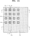
- FIGS. 1A through 1G are plan views of a semiconductor device having a vertical channel according to an embodiment of the present invention.
- FIGS. 2A through 2H are cross-sectional views of the semiconductor device having the vertical channel according to an embodiment of the present invention, which are taken along the lines x-x′ of FIGS. 1A through 1G ;
- FIGS. 3A through 3H are cross-sectional views of the semiconductor device having the vertical channel according to an embodiment of the present invention taken along the lines y-y′ of FIGS. 1A through 1G ;
- FIGS. 4A through 4H are cross-sectional views of the semiconductor device having the vertical channel according to an embodiment of the present invention taken along lines z-z′ of FIGS. 1A through 1G ;
- FIGS. 5A through 5E are plan views of a semiconductor device having a vertical channel according to another embodiment of the present invention.
- FIGS. 6A through 6E are cross-sectional views of the semiconductor device having the vertical channel according to another embodiment of the present invention taken along lines x-x′ of FIGS. 5A through 5E ;
- FIGS. 7A through 7E are cross-sectional views of the semiconductor device having the vertical channel according to another embodiment of the present invention taken along lines y-y′ of FIGS. 5A through 5E ;
- FIGS. 8A and 8B are plan views of a semiconductor device having a vertical channel using damascene process according to another embodiment of the present invention.
- FIGS. 9A through 9C are cross-sectional views of the semiconductor device having the vertical channel using damascene process according to another embodiment of the present invention taken along lines x-x′ of FIGS. 8A and 8B ;
- FIGS. 10A through 10C are cross-sectional views of the semiconductor device having the vertical channel using damascene process according to another embodiment of the present invention taken along lines y-y′ of FIGS. 8A and 8B .
- a pad oxide layer 105 is formed on a semiconductor substrate 100 , and a plurality of hard mask patterns 110 are formed on the pad oxide layer 105 .
- a silicon oxide layer or a silicon oxynitride layer may be used as hard mask pattern 110 which are spaced apart from each other by predetermined distances in the x-x′ direction (hereinafter, referred to as “row direction”) and y-y′ direction (hereinafter, referred to as “column direction”), respectively.
- the width of one side of the hard mask pattern 110 may be, for example, a minimum feature size of 1F and the distance between adjacent hard mask patterns 110 may also be 1F. Therefore, a cell area that one unit cell having one hard mask pattern 110 occupies is 4F2.
- An exposed semiconductor substrate 100 is etched to a relatively shallow depth for example, in a range of about 100 ⁇ to 300 ⁇ , using the hard mask pattern 110 .
- a first insulating spacer 115 is formed such that it surrounds both the hard mask pattern 110 and the sidewall of the exposed semiconductor substrate 100 .
- the semiconductor substrate 100 is then dry-etched to a predetermined depth, for example, in the range of about 800 ⁇ to 1,500 ⁇ using hard mask pattern 110 and the first insulating spacer 115 as a mask to form an upper pillar (or a preliminary pillar) 100 a .
- Sidewall of exposed upper pillar 100 a is isotropically etched using first insulating spacer 115 as a mask to form isotropic space S 1 .
- the isotropic etching may be performed such that an etched depth is in the range of about 150 ⁇ to 500 ⁇ .
- the first insulating spacer 115 positions isotropic space S 1 at a position spaced apart from the upper portion of upper pillar 100 a by a predetermined distance.
- a sacrificial gate insulating layer 120 is formed on the surface of semiconductor substrate 100 in which isotropic space S 1 is provided. Thereafter, a gate material is deposited to a predetermined thickness to fill isotropic space S 1 on the semiconductor substrate 100 on which the sacrificial gate insulating layer 120 is formed.
- the gate material may be, for example, polysilicon doped with n-type impurities, polysilicon doped with p-type impurities, silicon germanium, metal, metal silicide, etc.
- the gate material is anisotropically etched such that the hard mask pattern 110 and the sacrificial gate insulating layer 120 are exposed to form a sacrificial gate electrode 125 in isotropic space S 1 wherein the sacrificial gate electrode 125 surrounds the upper pillar 100 a .
- Impurities are implanted into the semiconductor substrate 100 between the upper pillars 100 a surrounded by the sacrificial gate electrode 125 so as to form a bottom source/drain region 130 .
- the implanted impurities may be, for example, phosphorus ions (31P) or arsenic ions (75As).
- the surface of the semiconductor substrate 100 into which the impurities are implanted is covered with the sacrificial gate insulating layer 120 .
- a second insulating spacer 135 is formed on respective sidewalls of first insulating spacer 115 and sacrificial gate electrode 125 .
- the second insulating spacer 135 may also be formed of a silicon oxide layer similar to first insulating spacer 115 .
- a capping layer 132 formed of a silicon nitride layer may be additionally formed on the respective sidewalls of the first insulating spacer 115 and the sacrificial gate electrode 125 before formation of second insulating layer 135 .
- a predetermined portion of semiconductor substrate 100 including the exposed bottom source/drain region 130 is etched to a desired depth using the second insulating spacer 135 as a mask to form active pillar 140 .
- the formation of the active pillar 140 disposes the bottom source/drain region 130 in a particular row to be separate from the bottom source/drain region in other rows. In this manner, each source/drain region of a particular row is isolated.
- An embedded bit line 150 is selectively formed on the exposed semiconductor substrate 100 between active pillars 140 .
- the embedded bit line 150 may be formed through a selective silicide process after depositing a transition metal layer.
- the embedded bit line 150 is self-aligned by sacrificial gate electrode 125 and second insulating spacer 135 disposed on the sidewall thereof. Since the embedded bit line 150 is defined by second insulating spacer 135 having a uniform linewidth, it has a uniform width and thus, a uniform resistance distribution.
- a first interlayer insulating layer 155 is deposited over the resultant structure of the semiconductor substrate 100 and planarized such that the hard mask 110 is exposed. The first interlayer insulating layer 155 may have the same etch selectivity as second insulating spacer 135 .
- first interlayer insulating layer 155 and second insulating spacer 135 are etched to a predetermined thickness such that the sidewall of sacrificial gate electrode 125 is partially exposed.
- the etching of the first interlayer insulating layer 155 may be performed using a wet etching process.
- the dotted section denotes an upper portion of first interlayer insulating layer 155 before the etching process and a reference numeral 155 a denotes a residue of the first interlayer insulating layer 155 after the etching process.
- Capping layer 132 plays a role in preventing the first insulating spacer 115 and the sacrificial gate insulating layer 120 from being lifted off while first interlayer insulating layer 155 is wet-etched.
- capping layer 132 is removed sacrificial gate electrode 125 is exposed and selectively removed so that isotropic space S 1 is again provided in active pillar 140 .
- Bottom source/drain region 130 and embedded bit line 150 are shielded by first interlayer insulating layer 155 a.
- gate insulating layer 158 is formed by a deposition process or oxidation process using, for example, silicon oxide (SiO2) layer, a hafnium oxide (HfO2) layer, a tantalum oxide (Ta2O5) layer, an oxide/nitride (ON) layer, an oxide/nitride/oxide (ONO) layer, or the like.
- Word line material 160 is deposited such that it sufficiently fills isotropic space SI and the space between active pillars 140 .
- Word line material 160 is planarized to expose the top surface of hard mask pattern 110 .
- Word line material 160 may be formed as a polysilicon layer doped with n-type or p-type impurities, a transition metal layer, a transition metal silicide layer, or a multi-stacked layer including at least one additional layer above.
- first word line mask pattern 165 is formed on word line material 160 where the mask pattern 165 may be extended in a direction perpendicular to the embedded bit line 150 , for example, in a row direction.
- First word line mask pattern 165 may be formed such that it shields at least one column of active pillars 140 .
- First word line mask pattern 165 may be formed in every column in a memory device such as a DRAM.
- a photoresist layer or a hard mask layer may be used as word line mask pattern 165 .
- word line material 160 is anisotropically etched using first word line mask pattern 165 and hard mask pattern 110 so that a ring-shaped gate electrode 161 a and a preliminary word line 161 b are formed.
- the ring-shaped gate electrode 161 a is formed in isotropic space S 1 of active pillar 140 and preliminary word line 161 b is integrally formed with ring-shaped gate electrode 161 a . That is, in the area that first word line mask pattern 165 does not exist, the word line material 160 is anisotropically etched corresponding to hard mask pattern 110 to form only ring-shaped gate electrode 161 surrounding active pillar 140 .
- preliminary word line 161 b is simultaneously formed with ring-shaped gate electrode 161 a , wherein the preliminary word line 161 b extends in the shape associated with first word line mask pattern 165 .
- Ring-shaped gate electrode 161 a and preliminary word line 161 b are integrally formed from the same material. In this manner, no contact interface is present which significantly differs from the prior art.
- First word line mask pattern 165 is then removed and second interlayer insulating layer 170 is formed on the resultant structure of semiconductor substrate 100 on which the ring-shaped gate electrode 161 a and the preliminary word line 161 b are formed. Second interlayer insulating layer 170 is planarized such that the hard mask pattern 110 is exposed.
- a second word line mask pattern 175 is formed to expose the region where preliminary word line 161 b has been formed.
- Second word line mask pattern 175 has a phase opposite to first word line mask pattern 165 so that it is formed using a reverse type photoresist while using only one reticle or mask.
- the exposed preliminary word line 161 b is then etched to a predetermined thickness to form word line 161 c .
- the top surface of word line 161 c may be disposed on a plane lower than the top surface of active pillar 140 .
- top surface of word line 161 c may be equal in height to or lower than the top surface of ring-shaped gate electrode 161 a .
- the gate electrode 161 a and word line 161 c are formed through a single process using the same material, no interface exists between the gate electrode 161 a and word line 161 c , thereby the contact resistance is reduced.
- second word line mask pattern 175 is removed by a well-known process and third interlayer insulating layer 180 is formed over exposed word line 161 c .
- third interlayer insulating layer 180 is then planarized. After forming the gate electrode 125 , the bottom source/drain region 130 and the embedded bit line 150 by a self-aligning scheme, sacrificial gate electrode 125 is removed.
- Ring-shaped gate electrode 161 a and word line 161 c connecting ring-shaped electrodes 161 a are simultaneously formed in the region where sacrificial gate electrode 125 is removed. Accordingly, it is possible to reduce the contact resistance because the contact interface does not exist between the gate electrode 161 a and the word line 161 c.
- ring-shaped gate electrode 161 a and word line 161 c may be integrally formed without using sacrificial gate electrode 125 in an embodiment in accordance with the present invention.
- FIGS. 5A , 6 A, and 7 A the manufacturing processes are the same as those of the aforementioned embodiment with the exception of the formation of upper pillar 200 a .
- FIGS illustrate semiconductor substrate 200 , pad oxide layer 205 , hard mask layer 210 and first insulating spacer 215 .
- signal line 222 is selectively formed on the bottom source/drain region 220 .
- Signal line 222 is a conductive layer that becomes a bit line using a predetermined patterning process to form a conductive layer such as a silicide layer on the bottom source/drain region 220 .
- First interlayer insulating layer 225 is formed over the resultant structure such that it sufficiently fills the space between upper pillars 200 a.
- a bit line mask pattern (not shown) is formed on first interlayer insulating layer 225 by well-known photolithography processes.
- the bit line mask pattern is formed in each row to cover all the hard mask patterns 210 disposed in the same row, e.g., in direction x-x′.
- the semiconductor substrate 200 incorporating first interlayer insulating layer 225 and the bottom source/drain region 220 is etched corresponding to the bit line mask pattern to define active pillar 230 and bit line 222 .
- active pillars 230 disposed in different rows are electrically isolated from one another.
- the bit line mask pattern is then removed by a well-known process.
- second interlayer insulating layer 235 is formed on semiconductor substrate 200 such that it sufficiently fills the space between active pillars 230 .
- Second interlayer insulating layer 235 is etched back to expose bottom source/drain region 220 .
- Second interlayer insulating layer 235 shown in FIG. 7C taken along the line y-y′ of FIG. 5C is buried between active pillars 230 .
- Sidewall of exposed active pillar 230 is isotropically etched to a predetermined thickness using hard mask pattern 210 and first insulating spacer 215 to form an isotropic space S 1 .
- gate oxide layer 240 is deposited on the exposed surface of semiconductor substrate 200 , i.e., the surface of active pillar 230 and the surface of the bottom source/drain region 220 incorporating bit line 222 .
- a word line material is then formed over the resultant structure which sufficiently fills isotropic space S 1 and the space between active pillars 230 .
- the word line material may be formed of a polysilicon layer, a transition metal layer, a transition metal nitride layer, a transition metal silicide layer, or a multi-stacked layer including at least one additional layer above.
- the word line material is planarized such that it becomes as high as hard mask pattern 210 .
- a word line mask pattern 250 is then formed on the word line material for simultaneously defining a word line and a gate electrode.
- Word line mask pattern 250 is formed perpendicular to bit line 222 and covers hard mask patterns 210 arranged in the same column. Although the word line mask pattern 250 is formed in every column in an alternative embodiment, the word line mask pattern 250 may be formed in a selected column similar to the embodiment referenced above.
- a photoresist layer or a hard mask layer may be used as word line mask pattern 250 .
- the word line material is anisotropically etched corresponding to word line mask pattern 250 to define a ring-shaped gate electrode 245 a and a preliminary word line 245 b .
- the ring-shaped gate electrode 245 a is buried in isotropic space S 1 of active pillar 230 and the preliminary word line 245 b crosses over bit line 222 .
- word line mask pattern 250 is removed and preliminary word line 245 b is etched back to a predetermined thickness so that preliminary word line 245 b becomes as high as ring-shaped gate electrode 245 a , thereby forming word line 245 c .
- Word line 245 c is integrally formed with ring-shaped gate electrode 245 a similar to the previous embodiment. In this manner, no contact interface is present between gate electrode 245 a and word line 245 c . Thus, it is possible to reduce the contact resistance caused by the contact interface.
- a third interlayer insulating layer 255 is formed over the resultant structure of the semiconductor substrate 200 such that adjacent active pillars 230 are electrically isolated from each other.
- Removing of the hard mask pattern and forming of a top source/drain region on the exposed active pillar 230 are performed so as to complete a semiconductor device having a vertical channel.
- these steps have been described in detail above and will not be described in connection with the present embodiment.
- Ring-shaped gate electrode 245 a and word line 245 c may be formed by a damascene process.
- FIGS. 8A and 8B are plan views of a semiconductor device having a vertical channel using a damascene process.
- FIGS. 9A through 9C are cross-sectional views taken along the lines x-x′ of FIGS. 8A and 8B
- FIGS. 10A through 10C are cross-sectional views taken along the lines y-y′ of FIGS. 8A and 8B .
- processes prior to a process illustrated in FIGS. 8A , 9 A and 10 A are identical to the processes illustrated in FIGS. 5A , 6 A and 7 A and FIGS. 5B , 6 B and 7 B and therefore, further descriptions have been omitted.
- second interlayer insulating layer 235 is deposited on semiconductor substrate 200 having an active pillar 230 so that the insulating layer fills the space between active pillars 230 .
- Second interlayer insulating layer 235 is planarized to expose hard mask pattern 210 .
- a damascene mask pattern (not shown) is formed on second interlayer insulating layer 235 to expose a predetermined region for a word line. The damascene mask pattern crosses over bit line 222 and exposes hard mask patterns 210 disposed in the same column.
- a width (W 1 ) of the exposed portion by the damascene mask pattern may be greater than the width (W 2 ) of the hard mask pattern 210 so that the sidewall of active pillar 230 can be exposed.
- second interlayer insulating layer 235 is anisotropically etched to a predetermined thickness corresponding to the shape of the damascene mask pattern. Second interlayer insulating layer 235 may be etched so that a predetermined thickness still remains on bit line 222 , as illustrated in FIG. 9A taken along line x-x′ of FIG. 8A .
- the damascene mask pattern is then removed by a well-known process.
- a word line material is formed on second interlayer insulating layer 235 such that it fills predetermined region PW for the word line.
- the word line material 245 and the second interlayer insulating layer 235 are etched back to expose first insulating layer 215 , but not too far to expose gate insulating layer 240 to integrally form gate electrode 245 a and a word line 245 c .
- the subsequent process steps are the same as those of the previously described.
- word line 245 c and gate electrode 245 a are integrally formed in predetermined region PW for the word line and a gate region (isotropic space) by a damascene process. Accordingly, there is no contact interface between gate electrode 245 a and word line 245 c .
- the word line is extended in y-y′ direction and the bit line is extended in x-x′ direction in the embodiments, it is not limited thereto. In particular, the word line may be extended in x-x′ direction and the bit line may be extended in y-y′ direction.
- both the embedded bit line 150 and bit line 222 formed by a selective scheme may also be utilized in any of the foregoing embodiments.
- a vertical channel transistor including a ring-shaped gate electrode surrounding an outer periphery of an active pillar, and bottom and top source/drain regions disposed under and over the ring-shaped gate electrode, the word line connecting the ring-shaped gate electrodes disposed in the same row or column is integrally formed with the ring-shaped gate electrode.
- the word line connecting the ring-shaped gate electrodes disposed in the same row or column is integrally formed with the ring-shaped gate electrode.
Landscapes
- Engineering & Computer Science (AREA)
- Microelectronics & Electronic Packaging (AREA)
- Power Engineering (AREA)
- Physics & Mathematics (AREA)
- Condensed Matter Physics & Semiconductors (AREA)
- General Physics & Mathematics (AREA)
- Computer Hardware Design (AREA)
- Ceramic Engineering (AREA)
- Manufacturing & Machinery (AREA)
- Semiconductor Memories (AREA)
Applications Claiming Priority (2)
| Application Number | Priority Date | Filing Date | Title |
|---|---|---|---|
| KR1020060012578A KR100734313B1 (ko) | 2006-02-09 | 2006-02-09 | 수직 채널을 갖는 반도체 소자 및 그 제조방법 |
| KR10-2006-0012578 | 2006-02-09 |
Publications (2)
| Publication Number | Publication Date |
|---|---|
| US20070181925A1 US20070181925A1 (en) | 2007-08-09 |
| US7776692B2 true US7776692B2 (en) | 2010-08-17 |
Family
ID=38333168
Family Applications (1)
| Application Number | Title | Priority Date | Filing Date |
|---|---|---|---|
| US11/702,601 Expired - Fee Related US7776692B2 (en) | 2006-02-09 | 2007-02-06 | Semiconductor device having a vertical channel and method of manufacturing same |
Country Status (3)
| Country | Link |
|---|---|
| US (1) | US7776692B2 (ko) |
| KR (1) | KR100734313B1 (ko) |
| CN (1) | CN101017825A (ko) |
Cited By (2)
| Publication number | Priority date | Publication date | Assignee | Title |
|---|---|---|---|---|
| US8614117B2 (en) | 2012-02-08 | 2013-12-24 | International Business Machines Corporation | Self-aligned process to fabricate a memory cell array with a surrounding-gate access transistor |
| US10943819B2 (en) * | 2018-12-20 | 2021-03-09 | Nanya Technology Corporation | Semiconductor structure having a plurality of capped protrusions |
Families Citing this family (38)
| Publication number | Priority date | Publication date | Assignee | Title |
|---|---|---|---|---|
| US7910986B2 (en) * | 2007-05-31 | 2011-03-22 | Elpida Memory, Inc. | Semiconductor memory device and data processing system |
| KR100924197B1 (ko) | 2007-10-30 | 2009-10-29 | 주식회사 하이닉스반도체 | 반도체 소자 및 그 제조 방법 |
| KR100967678B1 (ko) | 2007-11-22 | 2010-07-07 | 주식회사 하이닉스반도체 | 수직형 트랜지스터를 구비한 반도체 소자 및 그의 제조방법 |
| KR101179193B1 (ko) | 2007-12-07 | 2012-09-03 | 삼성전자주식회사 | 수직 채널 트랜지스터를 갖는 반도체 소자의 제조방법 |
| KR101045092B1 (ko) | 2007-12-21 | 2011-06-29 | 주식회사 하이닉스반도체 | 반도체 소자 제조 방법 |
| KR101073124B1 (ko) * | 2007-12-24 | 2011-10-12 | 주식회사 하이닉스반도체 | 수직 채널 트랜지스터의 필라 형성 방법 |
| KR100912965B1 (ko) * | 2007-12-24 | 2009-08-20 | 주식회사 하이닉스반도체 | 수직 채널 트랜지스터를 구비한 반도체 소자의 제조 방법 |
| KR100972900B1 (ko) | 2007-12-31 | 2010-07-28 | 주식회사 하이닉스반도체 | 반도체 소자 및 그 제조 방법 |
| KR101061174B1 (ko) | 2008-01-02 | 2011-09-01 | 주식회사 하이닉스반도체 | 수직형 트랜지스터를 구비한 반도체 소자의 제조방법 |
| KR101061176B1 (ko) | 2008-02-29 | 2011-09-01 | 주식회사 하이닉스반도체 | 반도체 소자의 제조방법 |
| KR100979360B1 (ko) * | 2008-03-13 | 2010-08-31 | 주식회사 하이닉스반도체 | 반도체 소자 및 그 제조 방법 |
| KR100949265B1 (ko) | 2008-04-01 | 2010-03-25 | 주식회사 하이닉스반도체 | 반도체 소자 제조 방법 |
| KR101094950B1 (ko) | 2008-04-01 | 2011-12-15 | 주식회사 하이닉스반도체 | 반도체 소자 제조 방법 |
| KR100971420B1 (ko) * | 2008-04-04 | 2010-07-21 | 주식회사 하이닉스반도체 | 반도체 소자 제조 방법 |
| KR100983693B1 (ko) * | 2008-04-10 | 2010-09-24 | 주식회사 하이닉스반도체 | 고집적 반도체 장치 내 수직형 트랜지스터의 제조 방법 |
| KR100973718B1 (ko) * | 2008-04-28 | 2010-08-04 | 주식회사 하이닉스반도체 | 반도체 소자의 필라 형성 방법 및 이를 이용한 수직 채널트랜지스터 형성 방법 |
| KR101062842B1 (ko) | 2008-04-30 | 2011-09-07 | 주식회사 하이닉스반도체 | 반도체 소자 및 그 제조 방법 |
| WO2009133623A1 (ja) * | 2008-05-02 | 2009-11-05 | 日本ユニサンティスエレクトロニクス株式会社 | 固体撮像素子 |
| KR101055747B1 (ko) | 2008-11-13 | 2011-08-11 | 주식회사 하이닉스반도체 | 수직 채널 트랜지스터를 구비하는 반도체 장치의 제조방법 |
| JP5491723B2 (ja) * | 2008-11-20 | 2014-05-14 | 株式会社東芝 | 電力用半導体装置 |
| KR101149043B1 (ko) | 2009-10-30 | 2012-05-24 | 에스케이하이닉스 주식회사 | 매립형 비트라인을 구비하는 반도체 장치 및 그 제조방법 |
| KR101569466B1 (ko) * | 2009-12-31 | 2015-11-17 | 삼성전자주식회사 | 반도체 기억 소자 및 그 형성 방법 |
| KR101140079B1 (ko) | 2010-07-13 | 2012-04-30 | 에스케이하이닉스 주식회사 | 수직형 트랜지스터를 포함하는 반도체 소자 및 그 형성방법 |
| KR20120043475A (ko) * | 2010-10-26 | 2012-05-04 | 에스케이하이닉스 주식회사 | 3차원 구조의 비휘발성 메모리 장치의 제조 방법 |
| US9041099B2 (en) * | 2011-04-11 | 2015-05-26 | Nanya Technology Corp. | Single-sided access device and fabrication method thereof |
| US9401363B2 (en) * | 2011-08-23 | 2016-07-26 | Micron Technology, Inc. | Vertical transistor devices, memory arrays, and methods of forming vertical transistor devices |
| US8934300B1 (en) * | 2013-11-07 | 2015-01-13 | Macronix International Co., Ltd. | Memory array structure and operating method and manufacturing method for the same |
| TWI506733B (zh) * | 2013-11-07 | 2015-11-01 | Macronix Int Co Ltd | 記憶體陣列結構與其操作方法與製造方法 |
| US9589962B2 (en) | 2014-06-17 | 2017-03-07 | Micron Technology, Inc. | Array of conductive vias, methods of forming a memory array, and methods of forming conductive vias |
| KR20160018221A (ko) * | 2014-08-08 | 2016-02-17 | 에스케이하이닉스 주식회사 | 3차원 반도체 집적 회로 장치 및 그 제조방법 |
| CN106298778A (zh) * | 2016-09-30 | 2017-01-04 | 中国科学院微电子研究所 | 半导体器件及其制造方法及包括该器件的电子设备 |
| US11081484B2 (en) | 2016-09-30 | 2021-08-03 | Institute of Microelectronics, Chinese Academy of Sciences | IC unit and method of manufacturing the same, and electronic device including the same |
| KR20180098446A (ko) * | 2017-02-24 | 2018-09-04 | 삼성전자주식회사 | 반도체 장치 및 이의 제조 방법 |
| CN109285836B (zh) * | 2018-08-28 | 2023-10-10 | 中国科学院微电子研究所 | 半导体存储设备及其制造方法及包括存储设备的电子设备 |
| CN111063684B (zh) * | 2019-12-06 | 2023-04-11 | 中国科学院微电子研究所 | 具有c形有源区的半导体装置及包括其的电子设备 |
| CN111261700A (zh) * | 2020-01-21 | 2020-06-09 | 中国科学院微电子研究所 | C形沟道部半导体器件及其制造方法及包括其的电子设备 |
| CN115249659B (zh) * | 2021-04-28 | 2024-05-03 | 长鑫存储技术有限公司 | 半导体结构的制作方法 |
| CN115249662B (zh) * | 2021-04-28 | 2024-05-17 | 长鑫存储技术有限公司 | 半导体结构及其制作方法 |
Citations (9)
| Publication number | Priority date | Publication date | Assignee | Title |
|---|---|---|---|---|
| US4974060A (en) * | 1988-02-03 | 1990-11-27 | Hitachi, Ltd. | Semiconductor integrated circuit device and method of manufacturing the same |
| KR0147584B1 (ko) | 1994-03-17 | 1998-08-01 | 윤종용 | 매몰 비트라인 셀의 제조방법 |
| US6018174A (en) * | 1998-04-06 | 2000-01-25 | Siemens Aktiengesellschaft | Bottle-shaped trench capacitor with epi buried layer |
| US6114725A (en) * | 1997-01-22 | 2000-09-05 | International Business Machines Corporation | Structure for folded architecture pillar memory cell |
| US6218236B1 (en) | 1999-01-28 | 2001-04-17 | International Business Machines Corporation | Method of forming a buried bitline in a vertical DRAM device |
| US6337497B1 (en) | 1997-05-16 | 2002-01-08 | International Business Machines Corporation | Common source transistor capacitor stack |
| US20050186740A1 (en) * | 2004-02-25 | 2005-08-25 | Samsung Electronics Co., Ltd. | Vertical transistor structure for use in semiconductor device and method of forming the same |
| US20070080385A1 (en) * | 2005-10-10 | 2007-04-12 | Samsung Electronics Co., Ltd. | Semiconductor device having vertical transistor and method of fabricating the same |
| US7531874B2 (en) * | 2006-06-19 | 2009-05-12 | Samsung Electronics Co., Ltd. | Field effect transistors including source/drain regions extending beneath pillars |
Family Cites Families (2)
| Publication number | Priority date | Publication date | Assignee | Title |
|---|---|---|---|---|
| JP3599873B2 (ja) * | 1996-01-26 | 2004-12-08 | 株式会社半導体エネルギー研究所 | 半導体装置の作製方法 |
| KR20050078145A (ko) * | 2004-01-30 | 2005-08-04 | 삼성전자주식회사 | 수직 채널을 갖는 전계 효과 트랜지스터를 포함하는반도체 소자 및 그 형성 방법 |
-
2006
- 2006-02-09 KR KR1020060012578A patent/KR100734313B1/ko not_active IP Right Cessation
-
2007
- 2007-01-30 CN CNA200710004792XA patent/CN101017825A/zh active Pending
- 2007-02-06 US US11/702,601 patent/US7776692B2/en not_active Expired - Fee Related
Patent Citations (9)
| Publication number | Priority date | Publication date | Assignee | Title |
|---|---|---|---|---|
| US4974060A (en) * | 1988-02-03 | 1990-11-27 | Hitachi, Ltd. | Semiconductor integrated circuit device and method of manufacturing the same |
| KR0147584B1 (ko) | 1994-03-17 | 1998-08-01 | 윤종용 | 매몰 비트라인 셀의 제조방법 |
| US6114725A (en) * | 1997-01-22 | 2000-09-05 | International Business Machines Corporation | Structure for folded architecture pillar memory cell |
| US6337497B1 (en) | 1997-05-16 | 2002-01-08 | International Business Machines Corporation | Common source transistor capacitor stack |
| US6018174A (en) * | 1998-04-06 | 2000-01-25 | Siemens Aktiengesellschaft | Bottle-shaped trench capacitor with epi buried layer |
| US6218236B1 (en) | 1999-01-28 | 2001-04-17 | International Business Machines Corporation | Method of forming a buried bitline in a vertical DRAM device |
| US20050186740A1 (en) * | 2004-02-25 | 2005-08-25 | Samsung Electronics Co., Ltd. | Vertical transistor structure for use in semiconductor device and method of forming the same |
| US20070080385A1 (en) * | 2005-10-10 | 2007-04-12 | Samsung Electronics Co., Ltd. | Semiconductor device having vertical transistor and method of fabricating the same |
| US7531874B2 (en) * | 2006-06-19 | 2009-05-12 | Samsung Electronics Co., Ltd. | Field effect transistors including source/drain regions extending beneath pillars |
Cited By (2)
| Publication number | Priority date | Publication date | Assignee | Title |
|---|---|---|---|---|
| US8614117B2 (en) | 2012-02-08 | 2013-12-24 | International Business Machines Corporation | Self-aligned process to fabricate a memory cell array with a surrounding-gate access transistor |
| US10943819B2 (en) * | 2018-12-20 | 2021-03-09 | Nanya Technology Corporation | Semiconductor structure having a plurality of capped protrusions |
Also Published As
| Publication number | Publication date |
|---|---|
| CN101017825A (zh) | 2007-08-15 |
| KR100734313B1 (ko) | 2007-07-02 |
| US20070181925A1 (en) | 2007-08-09 |
Similar Documents
| Publication | Publication Date | Title |
|---|---|---|
| US7776692B2 (en) | Semiconductor device having a vertical channel and method of manufacturing same | |
| US11696442B2 (en) | Vertical memory devices and methods of manufacturing the same | |
| US7348628B2 (en) | Vertical channel semiconductor devices and methods of manufacturing the same | |
| US7183164B2 (en) | Methods of reducing floating body effect | |
| US7696570B2 (en) | Transistors of semiconductor device having channel region in a channel-portion hole and methods of forming the same | |
| US7902026B2 (en) | Method of fabricating semiconductor device having vertical channel transistor | |
| US9209192B2 (en) | Semiconductor device and method of fabricating the same | |
| US11251188B2 (en) | Semiconductor memory device and a method of fabricating the same | |
| KR101552971B1 (ko) | 반도체 장치 및 그 제조 방법 | |
| US8906766B2 (en) | Method for manufacturing semiconductor device with first and second gates over buried bit line | |
| KR20230107960A (ko) | 반도체 소자 | |
| US20240276699A1 (en) | Semiconductor devices having landing pad structures | |
| US20240130116A1 (en) | Semiconductor device | |
| US11647627B2 (en) | Integrated circuit device | |
| US7351625B2 (en) | Recessed transistors and methods of forming the same | |
| KR20240127121A (ko) | 집적회로 장치 | |
| TW202434032A (zh) | 動態隨機存取記憶體及其製造方法 | |
| KR20090067594A (ko) | 수직채널트랜지스터를 구비한 반도체소자 및 그 제조 방법 |
Legal Events
| Date | Code | Title | Description |
|---|---|---|---|
| AS | Assignment |
Owner name: SAMSUNG ELECTRONICS CO., LTD., KOREA, REPUBLIC OF Free format text: ASSIGNMENT OF ASSIGNORS INTEREST;ASSIGNORS:YOON, JAE-MAN;KIM, BONG-SOO;SEO, HYEOUNG-WON;AND OTHERS;REEL/FRAME:018965/0970 Effective date: 20070115 |
|
| FPAY | Fee payment |
Year of fee payment: 4 |
|
| FEPP | Fee payment procedure |
Free format text: MAINTENANCE FEE REMINDER MAILED (ORIGINAL EVENT CODE: REM.) |
|
| LAPS | Lapse for failure to pay maintenance fees |
Free format text: PATENT EXPIRED FOR FAILURE TO PAY MAINTENANCE FEES (ORIGINAL EVENT CODE: EXP.); ENTITY STATUS OF PATENT OWNER: LARGE ENTITY |
|
| STCH | Information on status: patent discontinuation |
Free format text: PATENT EXPIRED DUE TO NONPAYMENT OF MAINTENANCE FEES UNDER 37 CFR 1.362 |
|
| FP | Lapsed due to failure to pay maintenance fee |
Effective date: 20180817 |