KR20180098446A - 반도체 장치 및 이의 제조 방법 - Google Patents
반도체 장치 및 이의 제조 방법 Download PDFInfo
- Publication number
- KR20180098446A KR20180098446A KR1020170024948A KR20170024948A KR20180098446A KR 20180098446 A KR20180098446 A KR 20180098446A KR 1020170024948 A KR1020170024948 A KR 1020170024948A KR 20170024948 A KR20170024948 A KR 20170024948A KR 20180098446 A KR20180098446 A KR 20180098446A
- Authority
- KR
- South Korea
- Prior art keywords
- insulating film
- source
- active
- gate electrode
- spacer
- Prior art date
- Legal status (The legal status is an assumption and is not a legal conclusion. Google has not performed a legal analysis and makes no representation as to the accuracy of the status listed.)
- Granted
Links
Images


Classifications
-
- H—ELECTRICITY
- H10—SEMICONDUCTOR DEVICES; ELECTRIC SOLID-STATE DEVICES NOT OTHERWISE PROVIDED FOR
- H10D—INORGANIC ELECTRIC SEMICONDUCTOR DEVICES
- H10D30/00—Field-effect transistors [FET]
- H10D30/60—Insulated-gate field-effect transistors [IGFET]
- H10D30/63—Vertical IGFETs
-
- H01L29/7827—
-
- H01L29/42368—
-
- H01L29/517—
-
- H01L29/66666—
-
- H—ELECTRICITY
- H10—SEMICONDUCTOR DEVICES; ELECTRIC SOLID-STATE DEVICES NOT OTHERWISE PROVIDED FOR
- H10D—INORGANIC ELECTRIC SEMICONDUCTOR DEVICES
- H10D30/00—Field-effect transistors [FET]
- H10D30/01—Manufacture or treatment
- H10D30/021—Manufacture or treatment of FETs having insulated gates [IGFET]
- H10D30/025—Manufacture or treatment of FETs having insulated gates [IGFET] of vertical IGFETs
-
- H—ELECTRICITY
- H10—SEMICONDUCTOR DEVICES; ELECTRIC SOLID-STATE DEVICES NOT OTHERWISE PROVIDED FOR
- H10D—INORGANIC ELECTRIC SEMICONDUCTOR DEVICES
- H10D30/00—Field-effect transistors [FET]
- H10D30/60—Insulated-gate field-effect transistors [IGFET]
- H10D30/67—Thin-film transistors [TFT]
- H10D30/6704—Thin-film transistors [TFT] having supplementary regions or layers in the thin films or in the insulated bulk substrates for controlling properties of the device
- H10D30/6713—Thin-film transistors [TFT] having supplementary regions or layers in the thin films or in the insulated bulk substrates for controlling properties of the device characterised by the properties of the source or drain regions, e.g. compositions or sectional shapes
-
- H—ELECTRICITY
- H10—SEMICONDUCTOR DEVICES; ELECTRIC SOLID-STATE DEVICES NOT OTHERWISE PROVIDED FOR
- H10D—INORGANIC ELECTRIC SEMICONDUCTOR DEVICES
- H10D30/00—Field-effect transistors [FET]
- H10D30/60—Insulated-gate field-effect transistors [IGFET]
- H10D30/67—Thin-film transistors [TFT]
- H10D30/6728—Vertical TFTs
-
- H—ELECTRICITY
- H10—SEMICONDUCTOR DEVICES; ELECTRIC SOLID-STATE DEVICES NOT OTHERWISE PROVIDED FOR
- H10D—INORGANIC ELECTRIC SEMICONDUCTOR DEVICES
- H10D30/00—Field-effect transistors [FET]
- H10D30/60—Insulated-gate field-effect transistors [IGFET]
- H10D30/67—Thin-film transistors [TFT]
- H10D30/6729—Thin-film transistors [TFT] characterised by the electrodes
- H10D30/673—Thin-film transistors [TFT] characterised by the electrodes characterised by the shapes, relative sizes or dispositions of the gate electrodes
- H10D30/6735—Thin-film transistors [TFT] characterised by the electrodes characterised by the shapes, relative sizes or dispositions of the gate electrodes having gates fully surrounding the channels, e.g. gate-all-around
-
- H—ELECTRICITY
- H10—SEMICONDUCTOR DEVICES; ELECTRIC SOLID-STATE DEVICES NOT OTHERWISE PROVIDED FOR
- H10D—INORGANIC ELECTRIC SEMICONDUCTOR DEVICES
- H10D30/00—Field-effect transistors [FET]
- H10D30/60—Insulated-gate field-effect transistors [IGFET]
- H10D30/67—Thin-film transistors [TFT]
- H10D30/6757—Thin-film transistors [TFT] characterised by the structure of the channel, e.g. transverse or longitudinal shape or doping profile
-
- H—ELECTRICITY
- H10—SEMICONDUCTOR DEVICES; ELECTRIC SOLID-STATE DEVICES NOT OTHERWISE PROVIDED FOR
- H10D—INORGANIC ELECTRIC SEMICONDUCTOR DEVICES
- H10D62/00—Semiconductor bodies, or regions thereof, of devices having potential barriers
- H10D62/10—Shapes, relative sizes or dispositions of the regions of the semiconductor bodies; Shapes of the semiconductor bodies
- H10D62/113—Isolations within a component, i.e. internal isolations
- H10D62/115—Dielectric isolations, e.g. air gaps
- H10D62/116—Dielectric isolations, e.g. air gaps adjoining the input or output regions of field-effect devices, e.g. adjoining source or drain regions
-
- H—ELECTRICITY
- H10—SEMICONDUCTOR DEVICES; ELECTRIC SOLID-STATE DEVICES NOT OTHERWISE PROVIDED FOR
- H10D—INORGANIC ELECTRIC SEMICONDUCTOR DEVICES
- H10D62/00—Semiconductor bodies, or regions thereof, of devices having potential barriers
- H10D62/10—Shapes, relative sizes or dispositions of the regions of the semiconductor bodies; Shapes of the semiconductor bodies
- H10D62/13—Semiconductor regions connected to electrodes carrying current to be rectified, amplified or switched, e.g. source or drain regions
- H10D62/149—Source or drain regions of field-effect devices
- H10D62/151—Source or drain regions of field-effect devices of IGFETs
-
- H—ELECTRICITY
- H10—SEMICONDUCTOR DEVICES; ELECTRIC SOLID-STATE DEVICES NOT OTHERWISE PROVIDED FOR
- H10D—INORGANIC ELECTRIC SEMICONDUCTOR DEVICES
- H10D62/00—Semiconductor bodies, or regions thereof, of devices having potential barriers
- H10D62/10—Shapes, relative sizes or dispositions of the regions of the semiconductor bodies; Shapes of the semiconductor bodies
- H10D62/17—Semiconductor regions connected to electrodes not carrying current to be rectified, amplified or switched, e.g. channel regions
- H10D62/213—Channel regions of field-effect devices
- H10D62/221—Channel regions of field-effect devices of FETs
- H10D62/235—Channel regions of field-effect devices of FETs of IGFETs
-
- H—ELECTRICITY
- H10—SEMICONDUCTOR DEVICES; ELECTRIC SOLID-STATE DEVICES NOT OTHERWISE PROVIDED FOR
- H10D—INORGANIC ELECTRIC SEMICONDUCTOR DEVICES
- H10D64/00—Electrodes of devices having potential barriers
- H10D64/01—Manufacture or treatment
- H10D64/013—Manufacture or treatment of electrodes having a conductor capacitively coupled to a semiconductor by an insulator
- H10D64/01302—Manufacture or treatment of electrodes having a conductor capacitively coupled to a semiconductor by an insulator the insulator being formed after the semiconductor body, the semiconductor being silicon
- H10D64/01304—Manufacture or treatment of electrodes having a conductor capacitively coupled to a semiconductor by an insulator the insulator being formed after the semiconductor body, the semiconductor being silicon characterised by the conductor
- H10D64/01324—Manufacture or treatment of electrodes having a conductor capacitively coupled to a semiconductor by an insulator the insulator being formed after the semiconductor body, the semiconductor being silicon characterised by the conductor characterised by the sectional shape, e.g. T or inverted-T
-
- H—ELECTRICITY
- H10—SEMICONDUCTOR DEVICES; ELECTRIC SOLID-STATE DEVICES NOT OTHERWISE PROVIDED FOR
- H10D—INORGANIC ELECTRIC SEMICONDUCTOR DEVICES
- H10D64/00—Electrodes of devices having potential barriers
- H10D64/01—Manufacture or treatment
- H10D64/018—Spacers formed inside holes at the prospective gate locations, e.g. holes left by removing dummy gates
-
- H—ELECTRICITY
- H10—SEMICONDUCTOR DEVICES; ELECTRIC SOLID-STATE DEVICES NOT OTHERWISE PROVIDED FOR
- H10D—INORGANIC ELECTRIC SEMICONDUCTOR DEVICES
- H10D64/00—Electrodes of devices having potential barriers
- H10D64/01—Manufacture or treatment
- H10D64/031—Manufacture or treatment of data-storage electrodes
-
- H—ELECTRICITY
- H10—SEMICONDUCTOR DEVICES; ELECTRIC SOLID-STATE DEVICES NOT OTHERWISE PROVIDED FOR
- H10D—INORGANIC ELECTRIC SEMICONDUCTOR DEVICES
- H10D64/00—Electrodes of devices having potential barriers
- H10D64/20—Electrodes characterised by their shapes, relative sizes or dispositions
- H10D64/27—Electrodes not carrying the current to be rectified, amplified, oscillated or switched, e.g. gates
- H10D64/311—Gate electrodes for field-effect devices
- H10D64/411—Gate electrodes for field-effect devices for FETs
- H10D64/511—Gate electrodes for field-effect devices for FETs for IGFETs
- H10D64/512—Disposition of the gate electrodes, e.g. buried gates
-
- H—ELECTRICITY
- H10—SEMICONDUCTOR DEVICES; ELECTRIC SOLID-STATE DEVICES NOT OTHERWISE PROVIDED FOR
- H10D—INORGANIC ELECTRIC SEMICONDUCTOR DEVICES
- H10D64/00—Electrodes of devices having potential barriers
- H10D64/20—Electrodes characterised by their shapes, relative sizes or dispositions
- H10D64/27—Electrodes not carrying the current to be rectified, amplified, oscillated or switched, e.g. gates
- H10D64/311—Gate electrodes for field-effect devices
- H10D64/411—Gate electrodes for field-effect devices for FETs
- H10D64/511—Gate electrodes for field-effect devices for FETs for IGFETs
- H10D64/514—Gate electrodes for field-effect devices for FETs for IGFETs characterised by the insulating layers
- H10D64/516—Gate electrodes for field-effect devices for FETs for IGFETs characterised by the insulating layers the thicknesses being non-uniform
-
- H—ELECTRICITY
- H10—SEMICONDUCTOR DEVICES; ELECTRIC SOLID-STATE DEVICES NOT OTHERWISE PROVIDED FOR
- H10D—INORGANIC ELECTRIC SEMICONDUCTOR DEVICES
- H10D64/00—Electrodes of devices having potential barriers
- H10D64/20—Electrodes characterised by their shapes, relative sizes or dispositions
- H10D64/27—Electrodes not carrying the current to be rectified, amplified, oscillated or switched, e.g. gates
- H10D64/311—Gate electrodes for field-effect devices
- H10D64/411—Gate electrodes for field-effect devices for FETs
- H10D64/511—Gate electrodes for field-effect devices for FETs for IGFETs
- H10D64/517—Gate electrodes for field-effect devices for FETs for IGFETs characterised by the conducting layers
- H10D64/519—Gate electrodes for field-effect devices for FETs for IGFETs characterised by the conducting layers characterised by their top-view geometrical layouts
-
- H—ELECTRICITY
- H10—SEMICONDUCTOR DEVICES; ELECTRIC SOLID-STATE DEVICES NOT OTHERWISE PROVIDED FOR
- H10D—INORGANIC ELECTRIC SEMICONDUCTOR DEVICES
- H10D64/00—Electrodes of devices having potential barriers
- H10D64/60—Electrodes characterised by their materials
- H10D64/66—Electrodes having a conductor capacitively coupled to a semiconductor by an insulator, e.g. MIS electrodes
- H10D64/68—Electrodes having a conductor capacitively coupled to a semiconductor by an insulator, e.g. MIS electrodes characterised by the insulator, e.g. by the gate insulator
- H10D64/691—Electrodes having a conductor capacitively coupled to a semiconductor by an insulator, e.g. MIS electrodes characterised by the insulator, e.g. by the gate insulator comprising metallic compounds, e.g. metal oxides or metal silicates
Landscapes
- Insulated Gate Type Field-Effect Transistor (AREA)
- Engineering & Computer Science (AREA)
- Manufacturing & Machinery (AREA)
Abstract
Description
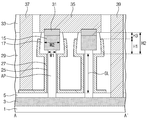
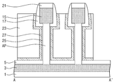
도 2는 도 1을 A-A' 선으로 자른 단면도이다.
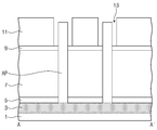
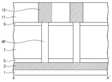
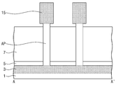
도 3 내지 도 15는 도 2의 단면을 가지는 반도체 장치를 제조하는 과정을 순차적으로 나타내는 공정 단면도들이다.
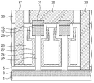
도 16 내지 도 18은 본 발명의 실시예들에 따른 반도체 장치들의 단면도들이다.
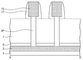
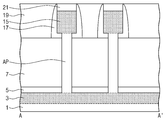
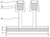
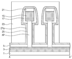
3: 제 1 소오스/드레인부
5, 29, 33: 절연막
7, 9, 11: 희생 절연막
13: 갭 영역
15: 제 2 소오스/드레인부
17: 스페이서
21: 캐핑 패턴
23: 마스크 패턴
25: 게이트 절연막
26: 고유전막
27: 게이트 전극
35: 상부전극
37: 게이트 전극 콘택
39: 하부전극 콘택
Claims (10)
- 기판으로부터 돌출된 활성 기둥;
상기 활성 기둥의 상단에 배치되며 상기 활성 기둥보다 넓은 폭을 가지는 제 1 소오스/드레인부;
상기 제 1 소오스/드레인부의 적어도 하부면을 덮는 스페이서;
상기 스페이서의 하부면과 상기 활성 기둥의 측면을 덮는 게이트 전극;
상기 게이트 전극과 상기 활성 기둥 사이에 개재된 게이트 절연막; 및
상기 활성 기둥 아래의 상기 기판 내에 배치되는 제 2 소오스/드레인부를 포함하는 반도체 장치. - 제 1 항에 있어서,
상기 스페이서는 연장되어 상기 제 1 소오스/드레인부의 측면을 일부 덮는 반도체 장치. - 제 1 항에 있어서,
상기 게이트 전극은 연장되어 상기 기판의 일부를 덮으며,
상기 게이트 전극과 상기 기판 사이에 개재되는 제 1 절연막을 더 포함하며,
상기 제 1 절연막은 상기 게이트 절연막보다 두꺼운 반도체 장치. - 제 1 항에 있어서,
상기 제 1 소오스/드레인부의 상부와 전기적으로 연결되는 상부전극을 더 포함하며,
상기 상부전극은 상기 게이트 전극과 이격되는 반도체 장치. - 제 4 항에 있어서,
상기 활성 기둥과 상기 제 1 소오스/드레인부는 복수개이며,
상기 상부전극은 복수개의 상기 제 1 소오스/드레인부들과 동시에 연결되는 반도체 장치. - 제 1 항에 있어서
상기 게이트 절연막은 고유전막을 포함하며,
상기 고유전막은 연장되어 상기 스페이서와 상기 게이트 전극 사이에 개재되는 반도체 장치. - 제 1 항에 있어서,
상기 활성 기둥은 복수개이며,
상기 게이트 전극은 연장되어 상기 활성 기둥들의 측면들을 덮는 반도체 장치. - 제 1 항에 있어서,
상기 활성 기둥과 상기 제 1 소오스/드레인부는 복수개이며,
상기 활성 기둥들 사이와 상기 제 1 소오스/드레인부들 사이를 채우며 상기 상부전극의 하부면과 접하는 제 1 층간절연막; 및
상기 제 1 층간절연막을 덮으며 상기 상부전극의 측면과 접하는 제 2 층간절연막을 더 포함하는 반도체 장치. - 반도체 기판의 표면으로부터 돌출된 활성 기둥을 형성하는 단계;
상기 활성 기둥 아래의 상기 반도체 기판에 제 1 소오스/드레인부를 형성하는 단계;
상기 반도체 기판 상에 제 1 절연막을 형성하여 상기 활성 기둥을 덮는 단계;
상기 제 1 절연막에 대하여 에치백 공정을 진행하여 상기 활성 기둥의 상부를 노출시키는 단계;
상기 노출된 상기 활성 기둥의 상부에 상기 활성 기둥보다 넓은 폭을 가지되 상기 제 1 절연막과 이격된 제 2 소오스/드레인부를 형성하는 단계;
상기 제 2 소오스/드레인부의 측벽과 하부면을 덮는 스페이서를 형성하는 단계;
상기 제 1 절연막을 제거하여 상기 스페이서의 하부면과 상기 활성 기둥의 측벽을 노출시키는 단계; 및
상기 스페이서의 하부면과 상기 활성 기둥의 측벽을 덮는 게이트 전극을 형성하는 단계를 포함하는 반도체 장치의 제조 방법. - 제 9 항에 있어서,
상기 제 2 소오스/드레인부를 형성하는 단계는,
상기 노출된 활성 기둥의 상부와 상기 제 1 절연막의 상부면을 콘포말하게 덮는 제 2 절연막을 형성하는 단계;
상기 제 3 절연막을 형성하여 상기 활성 기둥의 측면의 상기 제 2 절연막을 덮되, 상기 활성 기둥 상의 상기 제 2 절연막을 노출시키는 단계;
이방성 식각 공정을 진행하여 상기 제 3 절연막과 상기 활성 기둥 사이의 상기 제 2 절연막을 제거하여 상기 활성기둥의 상부면과 상부 측벽을 노출시키되, 상기 제 1 절연막의 상부면과 접하는 상기 제 2 절연막을 남기는 단계; 및
선택적 에피택시얼 성장 공정을 진행하고 불순물을 도핑하여 상기 노출된 활성 기둥을 상기 제 2 소오스/드레인부로 만드는 단계를 포함하는 반도체 장치의 제조 방법.
Priority Applications (4)
| Application Number | Priority Date | Filing Date | Title |
|---|---|---|---|
| KR1020170024948A KR102773973B1 (ko) | 2017-02-24 | 2017-02-24 | 반도체 장치 및 이의 제조 방법 |
| US15/664,226 US10256324B2 (en) | 2017-02-24 | 2017-07-31 | Semiconductor devices having vertical transistors with aligned gate electrodes |
| CN201810156564.2A CN108511526B (zh) | 2017-02-24 | 2018-02-24 | 有带对准栅电极的垂直晶体管的半导体器件及其制造方法 |
| US16/284,843 US10559673B2 (en) | 2017-02-24 | 2019-02-25 | Semiconductor devices having vertical transistors with aligned gate electrodes |
Applications Claiming Priority (1)
| Application Number | Priority Date | Filing Date | Title |
|---|---|---|---|
| KR1020170024948A KR102773973B1 (ko) | 2017-02-24 | 2017-02-24 | 반도체 장치 및 이의 제조 방법 |
Publications (2)
| Publication Number | Publication Date |
|---|---|
| KR20180098446A true KR20180098446A (ko) | 2018-09-04 |
| KR102773973B1 KR102773973B1 (ko) | 2025-03-05 |
Family
ID=63246449
Family Applications (1)
| Application Number | Title | Priority Date | Filing Date |
|---|---|---|---|
| KR1020170024948A Active KR102773973B1 (ko) | 2017-02-24 | 2017-02-24 | 반도체 장치 및 이의 제조 방법 |
Country Status (3)
| Country | Link |
|---|---|
| US (2) | US10256324B2 (ko) |
| KR (1) | KR102773973B1 (ko) |
| CN (1) | CN108511526B (ko) |
Cited By (2)
| Publication number | Priority date | Publication date | Assignee | Title |
|---|---|---|---|---|
| KR20210043414A (ko) * | 2019-10-11 | 2021-04-21 | 삼성전자주식회사 | 수직 전계 효과 트랜지스터 장치 및 수직 전계 효과 트랜지스터 장치의 형성방법 |
| KR20210154602A (ko) * | 2020-06-12 | 2021-12-21 | 삼성전자주식회사 | 반도체 장치 및 그 제조 방법 |
Families Citing this family (10)
| Publication number | Priority date | Publication date | Assignee | Title |
|---|---|---|---|---|
| KR102273365B1 (ko) * | 2017-05-12 | 2021-07-06 | 씨투에이엠피에스 에이비 | 수직 금속 산화막 반도체 전계 효과 트랜지스터 및 이를 형성하는 방법 |
| US10199278B2 (en) * | 2017-05-30 | 2019-02-05 | International Business Machines Corporation | Vertical field effect transistor (FET) with controllable gate length |
| EP3454378A1 (en) * | 2017-09-08 | 2019-03-13 | IMEC vzw | A method for forming a vertical channel device, and a vertical channel device |
| US10297507B2 (en) * | 2017-10-17 | 2019-05-21 | International Business Machines Corporation | Self-aligned vertical field-effect transistor with epitaxially grown bottom and top source drain regions |
| US10672887B2 (en) * | 2017-12-12 | 2020-06-02 | International Business Machines Corporation | Vertical FET with shaped spacer to reduce parasitic capacitance |
| US10535754B2 (en) * | 2018-06-05 | 2020-01-14 | International Business Machines Corporation | Method and structure for forming a vertical field-effect transistor |
| US11640987B2 (en) * | 2021-02-04 | 2023-05-02 | Applied Materials, Inc. | Implant to form vertical FETs with self-aligned drain spacer and junction |
| US12369295B2 (en) | 2022-04-26 | 2025-07-22 | Changxin Memory Technologies, Inc. | Semiconductor structure and manufacturing method thereof |
| US12414285B2 (en) | 2022-04-26 | 2025-09-09 | Changxin Memory Technologies, Inc. | Semiconductor structure and manufacturing method thereof |
| US12342524B2 (en) * | 2022-04-26 | 2025-06-24 | Changxin Memory Technologies, Inc. | Method for fabricating semiconductor device and semiconductor device |
Citations (5)
| Publication number | Priority date | Publication date | Assignee | Title |
|---|---|---|---|---|
| KR20030058633A (ko) * | 2001-12-31 | 2003-07-07 | 주식회사 하이닉스반도체 | 수직형 트랜지스터 및 그 제조 방법 |
| KR20140030019A (ko) * | 2012-08-30 | 2014-03-11 | 타이완 세미콘덕터 매뉴팩쳐링 컴퍼니 리미티드 | 융기된 드레인 구조물을 갖는 전계 효과 트랜지스터를 위한 시스템 및 방법 |
| KR20160123972A (ko) * | 2015-04-17 | 2016-10-26 | 타이완 세미콘덕터 매뉴팩쳐링 컴퍼니 리미티드 | 수직방향 디바이스를 갖춘 2 포트 sram 셀 구조 |
| US20170243974A1 (en) * | 2016-01-28 | 2017-08-24 | International Business Machines Corporation | Vertical field effect transistors with protective fin liner during bottom spacer recess etch |
| US20180076093A1 (en) * | 2016-09-12 | 2018-03-15 | International Business Machines Corporation | Vertical transistors having different gate lengths |
Family Cites Families (23)
| Publication number | Priority date | Publication date | Assignee | Title |
|---|---|---|---|---|
| CN1157480A (zh) * | 1995-08-30 | 1997-08-20 | 摩托罗拉公司 | 用栅电极易处置隔层形成单边缓变沟道半导体器件的方法 |
| KR100660881B1 (ko) * | 2005-10-12 | 2006-12-26 | 삼성전자주식회사 | 수직 채널 트랜지스터를 구비한 반도체 소자 및 그 제조방법 |
| US20070148939A1 (en) | 2005-12-22 | 2007-06-28 | International Business Machines Corporation | Low leakage heterojunction vertical transistors and high performance devices thereof |
| KR100725370B1 (ko) * | 2006-01-05 | 2007-06-07 | 삼성전자주식회사 | 반도체 장치의 제조 방법 및 그에 의해 제조된 반도체 장치 |
| KR100734313B1 (ko) * | 2006-02-09 | 2007-07-02 | 삼성전자주식회사 | 수직 채널을 갖는 반도체 소자 및 그 제조방법 |
| JP5317343B2 (ja) | 2009-04-28 | 2013-10-16 | ユニサンティス エレクトロニクス シンガポール プライベート リミテッド | 半導体装置及びその製造方法 |
| KR100971411B1 (ko) | 2008-05-21 | 2010-07-21 | 주식회사 하이닉스반도체 | 반도체 장치의 수직 채널 트랜지스터 형성 방법 |
| CN102709190B (zh) * | 2012-05-24 | 2017-04-26 | 上海华虹宏力半导体制造有限公司 | Ldmos场效应晶体管及其制作方法 |
| FR2991100B1 (fr) | 2012-05-25 | 2014-06-27 | Commissariat Energie Atomique | Transistor a base de nanofil, procede de fabrication du transistor, composant semi-conducteur integrant le transistor, programme informatique et support d'enregistrement associes au procede de fabrication |
| US8969963B2 (en) * | 2012-10-12 | 2015-03-03 | International Business Machines Corporation | Vertical source/drain junctions for a finFET including a plurality of fins |
| JP2014135359A (ja) | 2013-01-09 | 2014-07-24 | Tokyo Institute Of Technology | 電界効果トランジスタ |
| US10276664B2 (en) * | 2014-02-10 | 2019-04-30 | Taiwan Semiconductor Manufacturing Company Limited | Semiconductor structures and methods for multi-dimension of nanowire diameter to improve drive current |
| JP6287473B2 (ja) * | 2014-03-28 | 2018-03-07 | Tdk株式会社 | ブリッジレス力率改善コンバータ |
| US9755033B2 (en) * | 2014-06-13 | 2017-09-05 | Taiwan Semiconductor Manufacturing Co., Ltd. | Semiconductor device and method of forming vertical structure |
| US9698261B2 (en) * | 2014-06-30 | 2017-07-04 | Taiwan Semiconductor Manufacturing Co., Ltd. | Vertical device architecture |
| US9406793B2 (en) * | 2014-07-03 | 2016-08-02 | Broadcom Corporation | Semiconductor device with a vertical channel formed through a plurality of semiconductor layers |
| US9911848B2 (en) * | 2014-08-29 | 2018-03-06 | Taiwan Semiconductor Manufacturing Co., Ltd. | Vertical transistor and method of manufacturing the same |
| CN104218089B (zh) * | 2014-09-10 | 2017-02-15 | 北京大学 | 阶梯栅介质双层石墨烯场效应晶体管及其制备方法 |
| US9373620B2 (en) * | 2014-09-12 | 2016-06-21 | Taiwan Semiconductor Manufacturing Co., Ltd. | Series connected transistor structure and method of manufacturing the same |
| TWI662625B (zh) * | 2015-01-19 | 2019-06-11 | 聯華電子股份有限公司 | 半導體元件及其製作方法 |
| US9349860B1 (en) | 2015-03-31 | 2016-05-24 | Taiwan Semiconductor Manufacturing Company, Ltd. | Field effect transistors and methods of forming same |
| US20160336324A1 (en) * | 2015-05-15 | 2016-11-17 | Qualcomm Incorporated | Tunnel field effect transistor and method of making the same |
| US10170616B2 (en) * | 2016-09-19 | 2019-01-01 | Globalfoundries Inc. | Methods of forming a vertical transistor device |
-
2017
- 2017-02-24 KR KR1020170024948A patent/KR102773973B1/ko active Active
- 2017-07-31 US US15/664,226 patent/US10256324B2/en active Active
-
2018
- 2018-02-24 CN CN201810156564.2A patent/CN108511526B/zh active Active
-
2019
- 2019-02-25 US US16/284,843 patent/US10559673B2/en active Active
Patent Citations (5)
| Publication number | Priority date | Publication date | Assignee | Title |
|---|---|---|---|---|
| KR20030058633A (ko) * | 2001-12-31 | 2003-07-07 | 주식회사 하이닉스반도체 | 수직형 트랜지스터 및 그 제조 방법 |
| KR20140030019A (ko) * | 2012-08-30 | 2014-03-11 | 타이완 세미콘덕터 매뉴팩쳐링 컴퍼니 리미티드 | 융기된 드레인 구조물을 갖는 전계 효과 트랜지스터를 위한 시스템 및 방법 |
| KR20160123972A (ko) * | 2015-04-17 | 2016-10-26 | 타이완 세미콘덕터 매뉴팩쳐링 컴퍼니 리미티드 | 수직방향 디바이스를 갖춘 2 포트 sram 셀 구조 |
| US20170243974A1 (en) * | 2016-01-28 | 2017-08-24 | International Business Machines Corporation | Vertical field effect transistors with protective fin liner during bottom spacer recess etch |
| US20180076093A1 (en) * | 2016-09-12 | 2018-03-15 | International Business Machines Corporation | Vertical transistors having different gate lengths |
Cited By (2)
| Publication number | Priority date | Publication date | Assignee | Title |
|---|---|---|---|---|
| KR20210043414A (ko) * | 2019-10-11 | 2021-04-21 | 삼성전자주식회사 | 수직 전계 효과 트랜지스터 장치 및 수직 전계 효과 트랜지스터 장치의 형성방법 |
| KR20210154602A (ko) * | 2020-06-12 | 2021-12-21 | 삼성전자주식회사 | 반도체 장치 및 그 제조 방법 |
Also Published As
| Publication number | Publication date |
|---|---|
| KR102773973B1 (ko) | 2025-03-05 |
| US10559673B2 (en) | 2020-02-11 |
| US20190189778A1 (en) | 2019-06-20 |
| CN108511526B (zh) | 2024-01-02 |
| US10256324B2 (en) | 2019-04-09 |
| US20180248018A1 (en) | 2018-08-30 |
| CN108511526A (zh) | 2018-09-07 |
Similar Documents
| Publication | Publication Date | Title |
|---|---|---|
| KR102773973B1 (ko) | 반도체 장치 및 이의 제조 방법 | |
| US9590038B1 (en) | Semiconductor device having nanowire channel | |
| US11710736B2 (en) | Semiconductor device and method of manufacturing the same | |
| KR102593561B1 (ko) | 반도체 소자 | |
| US8129777B2 (en) | Semiconductor device having a multi-channel type MOS transistor | |
| KR101882360B1 (ko) | 매립 게이트 구조물을 포함하는 반도체 장치 및 그 제조 방법 | |
| GB2395603A (en) | Multichannel TFT having gate formed around channels | |
| US10050114B2 (en) | Semiconductor device and method of manufacturing the same | |
| US10332898B2 (en) | Semiconductor device and method of manufacturing the same | |
| CN101017825A (zh) | 具有垂直沟道的半导体器件及其制造方法 | |
| KR102363250B1 (ko) | 반도체 소자 | |
| KR20190029942A (ko) | 수직 채널을 가지는 반도체 소자 및 그 제조 방법 | |
| US10192966B2 (en) | Semiconductor devices including recessed gate electrode portions | |
| KR20170137637A (ko) | 반도체 장치 및 그 제조 방법 | |
| KR102755165B1 (ko) | 반도체 소자 | |
| US12249648B2 (en) | Semiconductor device having spacer between contract patterns | |
| US20170033217A1 (en) | Semiconductor devices and methods of manufacturing the same | |
| US12389688B2 (en) | Semiconductor device having dielectric layers of varying thicknesses | |
| KR20230062467A (ko) | 반도체 구조 및 이의 제조 방법 | |
| CN110718548B (zh) | 半导体器件 | |
| KR102568718B1 (ko) | 반도체 장치 | |
| KR102907655B1 (ko) | 상부 채널 및 하부 채널을 갖는 반도체 소자 및 그 제조 방법 | |
| KR102667811B1 (ko) | 반도체 소자 | |
| KR102845847B1 (ko) | 반도체 장치 | |
| TW202040697A (zh) | 形成半導體裝置的方法 |
Legal Events
| Date | Code | Title | Description |
|---|---|---|---|
| PA0109 | Patent application |
Patent event code: PA01091R01D Comment text: Patent Application Patent event date: 20170224 |
|
| PG1501 | Laying open of application | ||
| A201 | Request for examination | ||
| PA0201 | Request for examination |
Patent event code: PA02012R01D Patent event date: 20220224 Comment text: Request for Examination of Application Patent event code: PA02011R01I Patent event date: 20170224 Comment text: Patent Application |
|
| E902 | Notification of reason for refusal | ||
| PE0902 | Notice of grounds for rejection |
Comment text: Notification of reason for refusal Patent event date: 20240411 Patent event code: PE09021S01D |
|
| E701 | Decision to grant or registration of patent right | ||
| PE0701 | Decision of registration |
Patent event code: PE07011S01D Comment text: Decision to Grant Registration Patent event date: 20241202 |
|
| GRNT | Written decision to grant | ||
| PR0701 | Registration of establishment |
Comment text: Registration of Establishment Patent event date: 20250224 Patent event code: PR07011E01D |
|
| PR1002 | Payment of registration fee |
Payment date: 20250225 End annual number: 3 Start annual number: 1 |
|
| PG1601 | Publication of registration |