KR20180098446A - Semiconductor device and Method of fabricating the same - Google Patents
Semiconductor device and Method of fabricating the same Download PDFInfo
- Publication number
- KR20180098446A KR20180098446A KR1020170024948A KR20170024948A KR20180098446A KR 20180098446 A KR20180098446 A KR 20180098446A KR 1020170024948 A KR1020170024948 A KR 1020170024948A KR 20170024948 A KR20170024948 A KR 20170024948A KR 20180098446 A KR20180098446 A KR 20180098446A
- Authority
- KR
- South Korea
- Prior art keywords
- insulating film
- source
- active
- gate electrode
- spacer
- Prior art date
- Legal status (The legal status is an assumption and is not a legal conclusion. Google has not performed a legal analysis and makes no representation as to the accuracy of the status listed.)
- Granted
Links
Images


Classifications
-
- H—ELECTRICITY
- H10—SEMICONDUCTOR DEVICES; ELECTRIC SOLID-STATE DEVICES NOT OTHERWISE PROVIDED FOR
- H10D—INORGANIC ELECTRIC SEMICONDUCTOR DEVICES
- H10D30/00—Field-effect transistors [FET]
- H10D30/60—Insulated-gate field-effect transistors [IGFET]
- H10D30/63—Vertical IGFETs
-
- H01L29/7827—
-
- H01L29/42368—
-
- H01L29/517—
-
- H01L29/66666—
-
- H—ELECTRICITY
- H10—SEMICONDUCTOR DEVICES; ELECTRIC SOLID-STATE DEVICES NOT OTHERWISE PROVIDED FOR
- H10D—INORGANIC ELECTRIC SEMICONDUCTOR DEVICES
- H10D30/00—Field-effect transistors [FET]
- H10D30/01—Manufacture or treatment
- H10D30/021—Manufacture or treatment of FETs having insulated gates [IGFET]
- H10D30/025—Manufacture or treatment of FETs having insulated gates [IGFET] of vertical IGFETs
-
- H—ELECTRICITY
- H10—SEMICONDUCTOR DEVICES; ELECTRIC SOLID-STATE DEVICES NOT OTHERWISE PROVIDED FOR
- H10D—INORGANIC ELECTRIC SEMICONDUCTOR DEVICES
- H10D30/00—Field-effect transistors [FET]
- H10D30/60—Insulated-gate field-effect transistors [IGFET]
- H10D30/67—Thin-film transistors [TFT]
- H10D30/6704—Thin-film transistors [TFT] having supplementary regions or layers in the thin films or in the insulated bulk substrates for controlling properties of the device
- H10D30/6713—Thin-film transistors [TFT] having supplementary regions or layers in the thin films or in the insulated bulk substrates for controlling properties of the device characterised by the properties of the source or drain regions, e.g. compositions or sectional shapes
-
- H—ELECTRICITY
- H10—SEMICONDUCTOR DEVICES; ELECTRIC SOLID-STATE DEVICES NOT OTHERWISE PROVIDED FOR
- H10D—INORGANIC ELECTRIC SEMICONDUCTOR DEVICES
- H10D30/00—Field-effect transistors [FET]
- H10D30/60—Insulated-gate field-effect transistors [IGFET]
- H10D30/67—Thin-film transistors [TFT]
- H10D30/6728—Vertical TFTs
-
- H—ELECTRICITY
- H10—SEMICONDUCTOR DEVICES; ELECTRIC SOLID-STATE DEVICES NOT OTHERWISE PROVIDED FOR
- H10D—INORGANIC ELECTRIC SEMICONDUCTOR DEVICES
- H10D30/00—Field-effect transistors [FET]
- H10D30/60—Insulated-gate field-effect transistors [IGFET]
- H10D30/67—Thin-film transistors [TFT]
- H10D30/6729—Thin-film transistors [TFT] characterised by the electrodes
- H10D30/673—Thin-film transistors [TFT] characterised by the electrodes characterised by the shapes, relative sizes or dispositions of the gate electrodes
- H10D30/6735—Thin-film transistors [TFT] characterised by the electrodes characterised by the shapes, relative sizes or dispositions of the gate electrodes having gates fully surrounding the channels, e.g. gate-all-around
-
- H—ELECTRICITY
- H10—SEMICONDUCTOR DEVICES; ELECTRIC SOLID-STATE DEVICES NOT OTHERWISE PROVIDED FOR
- H10D—INORGANIC ELECTRIC SEMICONDUCTOR DEVICES
- H10D30/00—Field-effect transistors [FET]
- H10D30/60—Insulated-gate field-effect transistors [IGFET]
- H10D30/67—Thin-film transistors [TFT]
- H10D30/6757—Thin-film transistors [TFT] characterised by the structure of the channel, e.g. transverse or longitudinal shape or doping profile
-
- H—ELECTRICITY
- H10—SEMICONDUCTOR DEVICES; ELECTRIC SOLID-STATE DEVICES NOT OTHERWISE PROVIDED FOR
- H10D—INORGANIC ELECTRIC SEMICONDUCTOR DEVICES
- H10D62/00—Semiconductor bodies, or regions thereof, of devices having potential barriers
- H10D62/10—Shapes, relative sizes or dispositions of the regions of the semiconductor bodies; Shapes of the semiconductor bodies
- H10D62/113—Isolations within a component, i.e. internal isolations
- H10D62/115—Dielectric isolations, e.g. air gaps
- H10D62/116—Dielectric isolations, e.g. air gaps adjoining the input or output regions of field-effect devices, e.g. adjoining source or drain regions
-
- H—ELECTRICITY
- H10—SEMICONDUCTOR DEVICES; ELECTRIC SOLID-STATE DEVICES NOT OTHERWISE PROVIDED FOR
- H10D—INORGANIC ELECTRIC SEMICONDUCTOR DEVICES
- H10D62/00—Semiconductor bodies, or regions thereof, of devices having potential barriers
- H10D62/10—Shapes, relative sizes or dispositions of the regions of the semiconductor bodies; Shapes of the semiconductor bodies
- H10D62/13—Semiconductor regions connected to electrodes carrying current to be rectified, amplified or switched, e.g. source or drain regions
- H10D62/149—Source or drain regions of field-effect devices
- H10D62/151—Source or drain regions of field-effect devices of IGFETs
-
- H—ELECTRICITY
- H10—SEMICONDUCTOR DEVICES; ELECTRIC SOLID-STATE DEVICES NOT OTHERWISE PROVIDED FOR
- H10D—INORGANIC ELECTRIC SEMICONDUCTOR DEVICES
- H10D62/00—Semiconductor bodies, or regions thereof, of devices having potential barriers
- H10D62/10—Shapes, relative sizes or dispositions of the regions of the semiconductor bodies; Shapes of the semiconductor bodies
- H10D62/17—Semiconductor regions connected to electrodes not carrying current to be rectified, amplified or switched, e.g. channel regions
- H10D62/213—Channel regions of field-effect devices
- H10D62/221—Channel regions of field-effect devices of FETs
- H10D62/235—Channel regions of field-effect devices of FETs of IGFETs
-
- H—ELECTRICITY
- H10—SEMICONDUCTOR DEVICES; ELECTRIC SOLID-STATE DEVICES NOT OTHERWISE PROVIDED FOR
- H10D—INORGANIC ELECTRIC SEMICONDUCTOR DEVICES
- H10D64/00—Electrodes of devices having potential barriers
- H10D64/01—Manufacture or treatment
- H10D64/013—Manufacture or treatment of electrodes having a conductor capacitively coupled to a semiconductor by an insulator
- H10D64/01302—Manufacture or treatment of electrodes having a conductor capacitively coupled to a semiconductor by an insulator the insulator being formed after the semiconductor body, the semiconductor being silicon
- H10D64/01304—Manufacture or treatment of electrodes having a conductor capacitively coupled to a semiconductor by an insulator the insulator being formed after the semiconductor body, the semiconductor being silicon characterised by the conductor
- H10D64/01324—Manufacture or treatment of electrodes having a conductor capacitively coupled to a semiconductor by an insulator the insulator being formed after the semiconductor body, the semiconductor being silicon characterised by the conductor characterised by the sectional shape, e.g. T or inverted-T
-
- H—ELECTRICITY
- H10—SEMICONDUCTOR DEVICES; ELECTRIC SOLID-STATE DEVICES NOT OTHERWISE PROVIDED FOR
- H10D—INORGANIC ELECTRIC SEMICONDUCTOR DEVICES
- H10D64/00—Electrodes of devices having potential barriers
- H10D64/01—Manufacture or treatment
- H10D64/018—Spacers formed inside holes at the prospective gate locations, e.g. holes left by removing dummy gates
-
- H—ELECTRICITY
- H10—SEMICONDUCTOR DEVICES; ELECTRIC SOLID-STATE DEVICES NOT OTHERWISE PROVIDED FOR
- H10D—INORGANIC ELECTRIC SEMICONDUCTOR DEVICES
- H10D64/00—Electrodes of devices having potential barriers
- H10D64/01—Manufacture or treatment
- H10D64/031—Manufacture or treatment of data-storage electrodes
-
- H—ELECTRICITY
- H10—SEMICONDUCTOR DEVICES; ELECTRIC SOLID-STATE DEVICES NOT OTHERWISE PROVIDED FOR
- H10D—INORGANIC ELECTRIC SEMICONDUCTOR DEVICES
- H10D64/00—Electrodes of devices having potential barriers
- H10D64/20—Electrodes characterised by their shapes, relative sizes or dispositions
- H10D64/27—Electrodes not carrying the current to be rectified, amplified, oscillated or switched, e.g. gates
- H10D64/311—Gate electrodes for field-effect devices
- H10D64/411—Gate electrodes for field-effect devices for FETs
- H10D64/511—Gate electrodes for field-effect devices for FETs for IGFETs
- H10D64/512—Disposition of the gate electrodes, e.g. buried gates
-
- H—ELECTRICITY
- H10—SEMICONDUCTOR DEVICES; ELECTRIC SOLID-STATE DEVICES NOT OTHERWISE PROVIDED FOR
- H10D—INORGANIC ELECTRIC SEMICONDUCTOR DEVICES
- H10D64/00—Electrodes of devices having potential barriers
- H10D64/20—Electrodes characterised by their shapes, relative sizes or dispositions
- H10D64/27—Electrodes not carrying the current to be rectified, amplified, oscillated or switched, e.g. gates
- H10D64/311—Gate electrodes for field-effect devices
- H10D64/411—Gate electrodes for field-effect devices for FETs
- H10D64/511—Gate electrodes for field-effect devices for FETs for IGFETs
- H10D64/514—Gate electrodes for field-effect devices for FETs for IGFETs characterised by the insulating layers
- H10D64/516—Gate electrodes for field-effect devices for FETs for IGFETs characterised by the insulating layers the thicknesses being non-uniform
-
- H—ELECTRICITY
- H10—SEMICONDUCTOR DEVICES; ELECTRIC SOLID-STATE DEVICES NOT OTHERWISE PROVIDED FOR
- H10D—INORGANIC ELECTRIC SEMICONDUCTOR DEVICES
- H10D64/00—Electrodes of devices having potential barriers
- H10D64/20—Electrodes characterised by their shapes, relative sizes or dispositions
- H10D64/27—Electrodes not carrying the current to be rectified, amplified, oscillated or switched, e.g. gates
- H10D64/311—Gate electrodes for field-effect devices
- H10D64/411—Gate electrodes for field-effect devices for FETs
- H10D64/511—Gate electrodes for field-effect devices for FETs for IGFETs
- H10D64/517—Gate electrodes for field-effect devices for FETs for IGFETs characterised by the conducting layers
- H10D64/519—Gate electrodes for field-effect devices for FETs for IGFETs characterised by the conducting layers characterised by their top-view geometrical layouts
-
- H—ELECTRICITY
- H10—SEMICONDUCTOR DEVICES; ELECTRIC SOLID-STATE DEVICES NOT OTHERWISE PROVIDED FOR
- H10D—INORGANIC ELECTRIC SEMICONDUCTOR DEVICES
- H10D64/00—Electrodes of devices having potential barriers
- H10D64/60—Electrodes characterised by their materials
- H10D64/66—Electrodes having a conductor capacitively coupled to a semiconductor by an insulator, e.g. MIS electrodes
- H10D64/68—Electrodes having a conductor capacitively coupled to a semiconductor by an insulator, e.g. MIS electrodes characterised by the insulator, e.g. by the gate insulator
- H10D64/691—Electrodes having a conductor capacitively coupled to a semiconductor by an insulator, e.g. MIS electrodes characterised by the insulator, e.g. by the gate insulator comprising metallic compounds, e.g. metal oxides or metal silicates
Landscapes
- Insulated Gate Type Field-Effect Transistor (AREA)
- Engineering & Computer Science (AREA)
- Manufacturing & Machinery (AREA)
Abstract
Description
본 발명은 반도체 장치 및 이의 제조 방법에 관한 것이다.The present invention relates to a semiconductor device and a method of manufacturing the same.
소형화, 다기능화 및/또는 낮은 제조 단가 등의 특성들로 인하여 반도체 장치는 전자 산업에서 중요한 요소로 각광 받고 있다. 반도체 장치들은 논리 데이터를 저장하는 반도체 기억 장치, 논리 데이터를 연산 처리하는 반도체 논리 장치, 및 기억 요소와 논리 요소를 포함하는 하이브리드(hybrid) 반도체 장치 등으로 구분될 수 있다.The miniaturization, multifunctionality and / or low manufacturing cost characteristics make semiconductor devices an important element in the electronics industry. Semiconductor devices can be classified into a semiconductor storage device for storing logic data, a semiconductor logic device for computing and processing logic data, and a hybrid semiconductor device including a storage element and a logic element.
반도체 소자는 빠른 동작 속도 및/또는 낮은 동작 전압 등이 요구되고 있다. 이러한 요구 특성들을 충족시키기 위하여 반도체 장치는 보다 고집적화 되고 있다. 반도체 장치의 고집적화가 심화될수록, 반도체 장치의 신뢰성이 저하될 수 있다. 하지만, 전자 산업이 고도로 발전함에 따라, 반도체 장치의 높은 신뢰성에 대한 요구가 증가되고 있다. 따라서, 반도체 장치의 신뢰성을 향상시키기 위한 많은 연구가 진행되고 있다.Semiconductor devices require high operating speeds and / or low operating voltages. Semiconductor devices are becoming more highly integrated to meet these demanding characteristics. As the degree of integration of the semiconductor device increases, the reliability of the semiconductor device may deteriorate. However, as the electronics industry is highly developed, the demand for high reliability of semiconductor devices is increasing. Therefore, much research has been conducted to improve the reliability of the semiconductor device.
본 발명이 해결하고자 하는 과제는 균일한 문턱전압들을 가지는 수직 전계 효과 트랜지스터들을 포함하는 반도체 장치를 제공하는데 있다.SUMMARY OF THE INVENTION It is an object of the present invention to provide a semiconductor device including vertical field effect transistors having uniform threshold voltages.
본 발명이 해결하고자 하는 다른 과제는 게이트 길이(유효 게이트 길이)의 산포를 줄일 수 있는 반도체 장치의 제조 방법을 제공하는데 있다. Another object of the present invention is to provide a method of manufacturing a semiconductor device capable of reducing scattering of a gate length (effective gate length).
상기 과제를 달성하기 위한 본 발명에 실시예들에 따른 반도체 장치는, 기판으로부터 돌출된 활성 기둥; 상기 활성 기둥의 상단에 배치되며 상기 활성 기둥보다 넓은 폭을 가지는 제 1 소오스/드레인부; 상기 제 1 소오스/드레인부의 적어도 하부면을 덮는 스페이서; 적어도 상기 스페이서의 하부면과 상기 활성 기둥의 측면을 덮는 게이트 전극; 상기 게이트 전극과 상기 활성 기둥 사이에 개재된 게이트 절연막; 및 상기 활성 기둥 아래의 상기 기판 내에 배치되는 제 2 소오스/드레인부를 포함한다.According to an aspect of the present invention, there is provided a semiconductor device comprising: an active column protruded from a substrate; A first source / drain disposed at an upper end of the active column and having a width greater than that of the active column; A spacer covering at least the lower surface of the first source / drain portion; A gate electrode covering at least a lower surface of the spacer and a side surface of the active column; A gate insulating film interposed between the gate electrode and the active column; And a second source / drain portion disposed in the substrate under the active column.
상기 다른 과제를 달성하기 위한 본 발명에 실시예들에 따른 반도체 장치의 제조 방법은, 반도체 기판을 패터닝하여 반도체 기판의 표면으로부터 돌출된 활성 기둥을 형성하는 단계; 상기 활성 기둥 아래의 상기 반도체 기판에 제 1 소오스/드레인부를 형성하는 단계; 상기 반도체 기판 상에 제 1 절연막을 형성하여 상기 활성 기둥을 덮는 단계; 상기 제 1 절연막에 대하여 에치백 공정을 진행하여 상기 활성 기둥의 상부를 노출시키는 단계; 상기 노출된 상기 활성 기둥의 상부에 상기 활성 기둥보다 넓은 폭을 가지되 상기 제 1 절연막과 이격된 제 2 소오스/드레인부를 형성하는 단계; 상기 제 2 소오스/드레인부의 측벽과 하부면을 덮는 스페이서를 형성하는 단계; 상기 제 1 절연막을 제거하여 상기 스페이서의 하부면과 상기 활성 기둥의 측벽을 노출시키는 단계; 및 적어도 상기 스페이서의 하부면과 상기 활성 기둥의 측벽을 덮는 게이트 전극을 형성하는 단계를 포함한다. According to another aspect of the present invention, there is provided a method of manufacturing a semiconductor device, comprising: patterning a semiconductor substrate to form an active column protruding from a surface of the semiconductor substrate; Forming a first source / drain portion on the semiconductor substrate under the active pillars; Forming a first insulating film on the semiconductor substrate to cover the active column; Performing an etch-back process on the first insulating film to expose an upper portion of the active column; Forming a second source / drain portion having a width larger than that of the active column and spaced apart from the first insulating film on the exposed active pillars; Forming a spacer covering the side wall and the bottom surface of the second source / drain portion; Removing the first insulating film to expose a lower surface of the spacer and a side wall of the active column; And forming a gate electrode covering at least the lower surface of the spacer and the side wall of the active column.
본 발명의 실시예들에 따른 반도체 장치는 활성 기둥 상의 소오스/드레인부의 적어도 하부면을 덮는 스페이서를 포함하며, 게이트 전극이 상기 활성 기둥의 측면과 적어도 상기 스페이서의 하부면을 덮는다. 상기 스페이서에 의해 수직 전계 효과 트랜지스터들의 유효 게이트 길이들이 일정하게 되어 일정한 문턱전압을 나타낼 수 있다. A semiconductor device according to embodiments of the present invention includes a spacer covering at least a lower surface of a source / drain portion on an active column, and a gate electrode covers at least a side surface of the active column and at least a lower surface of the spacer. The effective gate lengths of the vertical field effect transistors may be constant by the spacers to exhibit a constant threshold voltage.
본 발명의 실시예들에 따른 반도체 장치의 제조 방법에서는, 후속에 형성되는 트랜지스터의 유효 게이트 길이를, 에치백된 희생 절연막의 두께로써 결정할 수 있다. 절연막을 식각하는 과정은 게이트 전극을 구성하는 금속을 식각하는 과정보다 컨트롤하기가 용이하여, 상대적으로 매우 적은 산포를 가진다. 따라서 최종 형성되는 트랜지스터들의 유효 게이트 길이의 산포를 상대적으로 줄일 수 있다. In the method of manufacturing a semiconductor device according to the embodiments of the present invention, the effective gate length of the transistor to be formed subsequently can be determined by the thickness of the sacrificial insulating film etched back. The process of etching the insulating film is easier to control than the process of etching the metal constituting the gate electrode, and has a relatively small scatter. Accordingly, the scattering of the effective gate length of the final formed transistors can be relatively reduced.
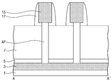
도 1은 본 발명의 실시예들에 따른 반도체 장치의 평면도이다.
도 2는 도 1을 A-A' 선으로 자른 단면도이다.
도 3 내지 도 15는 도 2의 단면을 가지는 반도체 장치를 제조하는 과정을 순차적으로 나타내는 공정 단면도들이다.
도 16 내지 도 18은 본 발명의 실시예들에 따른 반도체 장치들의 단면도들이다.1 is a plan view of a semiconductor device according to embodiments of the present invention.
2 is a sectional view taken along the line AA 'in Fig.
FIGS. 3 to 15 are process sectional views sequentially showing a process of manufacturing the semiconductor device having the section of FIG.
16 to 18 are sectional views of semiconductor devices according to embodiments of the present invention.
이하, 본 발명을 보다 구체적으로 설명하기 위하여 본 발명에 따른 실시예들을 첨부 도면을 참조하면서 보다 상세하게 설명하고자 한다. Hereinafter, embodiments of the present invention will be described in detail with reference to the accompanying drawings.
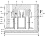
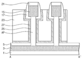
도 1은 본 발명의 실시예들에 따른 반도체 장치의 평면도이다. 도 2는 도 1을 A-A' 선으로 자른 단면도이다.1 is a plan view of a semiconductor device according to embodiments of the present invention. Fig. 2 is a cross-sectional view taken along line A-A 'of Fig. 1;
도 1 및 도 2를 참조하면, 반도체 기판(1)로부터 활성 기둥들(AP)이 돌출된다. 상기 반도체 기판(1)은 예를 들면 실리콘(Si) 기판, 저마늄(Ge) 기판, 실리콘-저마늄 기판, Ⅱ-Ⅵ족 화합물 반도체 기판, 또는 Ⅲ-Ⅴ족 화합물 반도체 기판일 수 있다. 상기 활성 기둥들(AP)은 상기 반도체 기판(1)으로부터 형성될 수 있다. 상기 활성 기둥들(AP) 아래의 상기 반도체 기판(1)에는 제 1 소오스/드레인부(3)가 배치된다. 상기 제 1 소오스/드레인부(3)에는 N형 또는 P형의 불순물이 도핑될 수 있다. 상기 제 1 소오스/드레인부(3)는 복수개의 활성 기둥들(AP)과 중첩될 수 있다. 상기 활성 기둥들(AP) 옆에 상기 반도체 기판(1) 상에는 제 1 절연막(5)이 배치된다. 상기 제 1 절연막(5)은 게이트 절연막(25) 보다 두꺼울 수 있다. 상기 제 1 절연막(5)은 질화막의 단일막이거나 또는 산화막과 질화막의 이중막일 수 있다. 이때 상기 제 1 절연막(5)을 구성하는 산화막은 상기 질화막과 상기 반도체 기판(1)사이의 스트레스를 완화시킬 수 있다. 상기 질화막은 후속의 패터닝 과정 중 식각 방지막의 역할을 할 수 있다. Referring to Figs. 1 and 2, active pillars AP are protruded from the
계속해서, 상기 활성 기둥들(AP) 상단에는 각각 제 2 소오스/드레인부(15)들이 배치된다. 상기 제 2 소오스/드레인부(15)도 상기 제 1 소오스/드레인부(3)와 동일하게 N형 또는 P형의 불순물이 도핑될 수 있다. 상기 활성 기둥(AP)의 제 1 폭(W1)은 상기 제 2 소오스/드레인부(15)의 제 2 폭(W2) 보다 좁다. 이로써 상기 제 2 소오스/드레인부(15)는 상기 활성 기둥(AP)의 양 옆으로 돌출될 수 있다. 상기 제 2 소오스/드레인부(15)의 하부면은 스페이서(17)로 덮인다. 상기 스페이서(17)는 상기 활성 기둥(AP)의 상부 측면과 접한다. 상기 스페이서(17)는 연장되어 상기 제 2 소오스/드레인부(15)의 측면과 접한다. 상기 제 2 소오스/드레인부(15) 상에는 오믹층(31)이 형성된다. 상기 오믹층(31)은 예를 들면 금속 실리사이드막일 수 있다. 상기 스페이서(17)는 연장되어 상기 오믹층(31)의 일부를 덮을 수 있다. 상기 스페이서(17)는 예를 들면 실리콘 질화막으로 형성될 수 있다. Subsequently, second source /
계속해서, 상기 활성 기둥(AP)의 측벽은 게이트 전극(27)으로 둘러싸인다. 상기 활성 기둥(AP)과 상기 게이트 전극(27) 사이에는 게이트 절연막(25)이 개재된다. 상기 게이트 전극(27)은 연장되어 상기 스페이서(17)의 하부면과 측벽의 일부를 덮을 수 있다. 상기 게이트 전극(27)은 연장되어 상기 제 1 절연막(5)의 상부면을 일부 덮을 수 있다. 본 예에서 상기 게이트 전극(27)은 연장되어 이웃하는 활성 기둥(AP)의 측벽을 둘러쌀 수 있다. 상기 게이트 전극(27)은 금속막을 포함할 수 있다. Subsequently, the side walls of the active pillars (AP) are surrounded by the gate electrode (27). A
상기 활성 기둥들(AP) 사이는 제 2 절연막(29)으로 채워진다. 상기 제 2 절연막(29)은 상기 스페이서(17)의 상부 측벽, 상기 게이트 전극(27) 및 상기 제 1 절연막(5)을 덮는다. 상기 제 2 절연막(29)은 상기 스페이서(17)의 상부면과 공면을 이루는 상부면을 가질 수 있다. 상기 제 2 절연막(29)은 제 3 절연막(33)으로 덮인다. 상기 제 3 절연막(33) 내에는 상부전극(35)이 배치되어 상기 오믹층(31)을 통해 상기 제 2 소오스/드레인부(15)와 전기적으로 연결된다. 상기 상부전극(35)은 상기 게이트 전극(27)과 이격된다. 상기 스페이서(17)의 하부면으로부터 상기 게이트 전극(27)의 상부면 까지의 제 1 수직 길이(H1)는 0 이상일 수 있다. 상기 스페이서(17)의 하부면으로부터 상부전극(35)의 하부면 까지의 제 2 수직 길이(H2)는 상기 제 1 수직 길이(H1) 보다 클 수 있다. 이로써 상기 게이트 전극(27)의 상부면으로부터 상기 상부전극(35)의 하부면 까지의 제 3 수직 길이(H3)는 0 초과가 되어, 상기 게이트 전극(27)은 상기 상부전극(35)으로부터 이격된다.The active pillars (AP) are filled with the second insulating film (29). The second
게이트 전극 콘택(37)은 상기 제 3 절연막(33)과 상기 제 2 절연막(29)을 관통하여 상기 제 1 절연막(5)을 덮는 상기 게이트 전극(27)과 접한다. 하부 전극 콘택(39)은 상기 제 3 절연막(33), 상기 제 2 절연막(29) 및 상기 제 1 절연막(5)을 관통하여 상기 제 1 소오스/드레인부(3)과 연결된다. The
상기 활성 기둥(AP)을 둘러싸는 상기 게이트 전극(27)과 상기 제 1 및 제 2 소오스 드레인부들(3, 15)은 하나의 수직 전계 효과 트랜지스터를 구성할 수 있다. 본 예에서 하나의 게이트 전극(27)은 이웃하는 두 개의 활성 기둥들(AP)을 동시에 둘러쌀 수 있으나, 경우에 따라 하나의 활성 기둥(AP)만을 둘러쌀 수도 있고, 세 개 이상의 활성 기둥들(AP)을 동시에 둘러쌀 수도 있다. 상기 제 1 및 제 2 소오스 드레인부들(3, 15)는 상기 활성 기둥(AP) 내부로 일부 침투할수도 있다. The
상기 수직 전계 트랜지스터에 있어서, 유효 게이트 길이(GL)는, 게이트 전극(GL)의 수직 길이가 아니라, 상기 제 1 절연막(5)의 상부면으로부터 상기 스페이서(17)의 하부면 까지의 수직 길이에 해당할 수 있다. 즉, 상기 유효 게이트 길이(GL)가 상기 스페이서(17)에 의해 결정된다. 여기서 유효 게이트 길이(GL)라 함은 하나의 수직 전계 효과 트랜지스터에서 게이트 전극(GL)이 활성 기둥(AP)에 인접하여 실질적으로 게이트 전극으로 기능을 할 수 있는 부분의 길이를 의미한다. 만약 상기 스페이서(17)가 없고, 게이트 전극(27)이 본 발명과 다르게 짧아, 활성 기둥의 일부만 덮도록 형성되는 경우에는 게이트 전극(27)의 수직 길이가 유효 게이트 길이와 동일해질 수 있다. 이 경우에는, 게이트 전극을 구성하는 금속을 식각할 때 발생하는 식각 산포에 의해 위치에 따라 유효 게이트 길이의 산포가 매우 크게 발생하게 된다. 그러나 스페이서(17)의 하부면의 높이는 절연막을 식각함으로써 결정될 수 있다. 절연막을 식각할 때 발생하는 식각 산포는 금속에 비하여 매우 적게 된다. 따라서 유효 게이트 길이의 산포가 작아지게 되어 문턱 전압의 산포도 줄일 수 있다. 상기 스페이서에 의해 수직 전계 효과 트랜지스터들의 유효 게이트 길이들이 일정하게 되어 일정한 문턱전압을 나타낼 수 있다. 또한 상기 제 2 소오스/드레인부(15)가 상기 활성 기둥(AP) 보다 넓은 폭을 가져 상기 트랜지스터의 구동시 저항을 줄일 수 있다. 상기 게이트 전극(27)이 상기 활성 기둥(AP)을 감싸므로 채널 전류를 증가시키며 쇼트 채널 효과를 해결할 수 있다. The effective gate length GL of the vertical electric field transistor is not a vertical length of the gate electrode GL but a vertical length from the upper surface of the first insulating
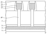
도 3 내지 도 15는 도 2의 단면을 가지는 반도체 장치를 제조하는 과정을 순차적으로 나타내는 공정 단면도들이다.FIGS. 3 to 15 are process sectional views sequentially showing a process of manufacturing the semiconductor device having the section of FIG.
도 3을 참조하면, 마스크 패턴(미도시)을 이용하여 반도체 기판(1)을 식각하여, 상기 반도체 기판(1)의 표면으로부터 돌출된 복수개의 활성 기둥들(AP)을 형성한다. 상기 활성 기둥들(AP)이 형성된 상기 반도체 기판(1) 상에 보호막(미도시)을 콘포말하게 형성한 후에, 이온 주입 공정을 진행하여 불순물을 상기 반도체 기판(1) 내에 주입한다. 그리고 어닐링 공정을 진행하여 상기 반도체 기판(1) 내에 주입된 불순물들을 확산시켜 상기 제 1 소오스/드레인부(3)를 형성한다. Referring to FIG. 3, the
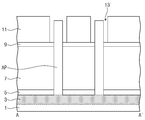
도 4를 참조하면, 상기 마스크 패턴(미도시)과 상기 보호막(미도시)을 제거한 후에, 상기 반도체 기판(1) 상에 제 1 절연막(5)을 형성하여 상기 활성 기둥들(AP)을 덮는다. 상기 제 1 절연막(5)은 예를 들면 실리콘 질화막 또는 차례로 적층된 실리콘 산화막과 실리콘 질화막으로 형성될 수 있다. 상기 제 1 절연막(5)에 대해 에치백 공정을 진행하여 상기 활성 기둥들(AP)의 측벽을 노출시키고 상기 반도체 기판(1) 상에 소정의 두께로 상기 제 1 절연막(5)을 남긴다. 상기 반도체 기판(1)의 전면 상에 제 1 희생 절연막(7)을 적층하여 상기 활성 기둥들(AP)을 덮는다. 상기 제 1 희생 절연막(7)은 예를 들면 상기 제 1 절연막(5) 및 상기 활성 기둥들(AP)과 식각 선택비를 가지는 물질로서, 예를 들면 실리콘 산화막으로 형성될 수 있다. 상기 제 1 희생 절연막(7)에 대해 에치백 공정을 진행하여 상기 활성 기둥들(AP)의 상부 측벽과 상부면을 노출시키되, 상기 활성 기둥들(AP)의 하부 측벽들 사이를 채우도록 제 1 희생 절연막(7)을 남긴다. 이때 남겨진 상기 제 1 희생 절연막(7)의 두께(T1)는 후속에 최종적으로 형성되는 수직 전계 트랜지스터의 유효 게이트 길이(도 2의 GL)과 동일/유사할 수 있다. 상기 제 1 희생 절연막(7)의 상부면의 높이는 후속에 형성되는 스페이서(17)의 하부면의 높이에 해당할 수 있다. 상기 제 1 희생 절연막(7)을 에치백 하는 과정에서 발생되는 식각 산포는 금속막을 식각하는 과정에서 발생되는 식각 산포의 거의 1/5~1/10 수준으로 매우 작다.Referring to FIG. 4, after removing the mask pattern (not shown) and the protective film (not shown), a first
도 5를 참조하여, 도 4의 상태에서 상기 반도체 기판(1)의 전면 상에 제 2 희생 절연막(9)을 콘포말하게 형성하여 상기 제 1 희생 절연막(7)의 상부면, 상기 활성 기둥(AP)의 측벽과 상부면을 덮는다. 상기 제 2 희생 절연막(9)은 상기 제 1 희생 절연막(7) 및 상기 활성 기둥(AP)와 동시에 식각 선택비를 가지는 물질로, 예를 들면 실리콘 질화막으로 형성될 수 있다. 상기 제 2 희생 절연막(9) 상에 제 3 희생 절연막(11)을 적층한 후 에치백이나 화학 기계적 연마 공정과 같은 평탄화 공정을 진행하여 상기 활성 기둥(AP) 상의 상기 제 2 희생 절연막(9)의 상부면을 노출시킨다. 상기 제 3 희생 절연막(11)은 예를 들면 실리콘 산화막으로 형성될 수 있다. 5, a second sacrificial insulating
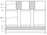
도 6을 참조하면, 노출된 상기 제 2 희생 절연막(9)에 대하여 이방성 식각 공정을 진행하여 상기 제 3 희생 절연막(11)과 상기 활성 기둥(AP) 사이의 상기 제 2 희생 절연막(9)을 제거하고 상기 제 3 희생 절연막(11)과 상기 제 1 희생 절연막(7) 사이에 상기 제 2 희생 절연막(9)을 남긴다. 이로써 상기 활성 기둥(AP)과 상기 제 3 희생 절연막(11)의 측면이 노출되고 이들 사이에 갭 영역(13)이 형성된다.6, an anisotropic etching process is performed on the exposed second
도 7을 참조하면, 선택적 에피택시얼 성장(Selective Epitaxial Growth) 방법을 이용하여 상기 갭 영역(13)에서 노출된 상기 활성 기둥(AP)의 표면으로부터 에피택시얼막을 성장시켜 상기 갭 영역(13)을 채운다. 상기 에피택시얼막은 상기 갭 영역(13) 밖으로 돌출될 수도 있다. 상기 갭 영역(13) 밖으로 돌출된 상기 에피택시얼막은 에치백 공정 등으로 제거할 수 있다. 이온주입 공정을 진행하여 상기 갭 영역(13) 안의 에피택시얼막에 불순물을 주입하여 제 2 소오스/드레인부(15)를 형성한다. 또는 상기 에피택시얼막을 성장시키는 동안 인시튜로 불순물을 도핑시킴으로써 상기 제 2 소오스/드레인부(15)를 형성할 수도 있다. 이로써 상기 제 2 소오스/드레인부(15)는 상기 활성 기둥(AP) 보다 넓은 폭을 가지도록 형성될 수 있다. 7, an epitaxial film is grown from the surface of the active pillar AP exposed in the
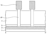
도 8을 참조하면, 상기 제 3 희생 절연막(11)과 상기 제 2 희생 절연막(9)을 순차적으로 제거하여 상기 제 2 소오스/드레인부(15)의 표면과 상기 활성 기둥(AP)의 상부 측면과 상기 제 1 희생 절연막(7)의 상부면을 노출시킨다. 이로써 상기 제 2 소오스/드레인부(15)의 하부면은 상기 제 1 희생 절연막(7)의 상부면으로부터 이격된다.8, the third
도 9를 참조하면, 도 8의 상태에서 상기 반도체 기판(1)의 전면 상에 스페이서막을 콘포말하게 형성하고 이방성 식각하여 상기 제 2 소오스/드레인부(15)의 측면을 덮는 스페이서(17)를 형성한다. 상기 스페이서(17)는 상기 제 2 소오스/드레인부(15)의 하부면과 상기 활성 기둥(AP)의 노출된 상부 측벽과 접하도록 형성된다. 상기 스페이서(17)은 예를 들면 실리콘 질화막으로 형성될 수 있다. 이로써 상기 스페이서(17)의 하부면의 높이는 상기 제 1 희생 절연막(7)의 상부면의 높이와 동일/유사해짐을 알 수 있다. Referring to FIG. 9, in the state of FIG. 8, a
도 10을 참조하면, 도 9의 상태에서 상기 반도체 기판(1)의 전면 상에 제 4 희생 절연막(19)을 적층하고 평탄화 공정을 진행하여 상기 제 2 소오스/드레인부(15)의 상부면을 노출시키는 동시에 상기 제 2 소오스/드레인부들(15) 사이의 공간을 채운다. 상기 제 4 희생 절연막(17)은 바람직하게는 상기 제 1 희생 절연막(7)과 동일한 물질로, 예를 들면 실리콘 산화막으로 형성될 수 있다. 노출된 상기 제 2 소오스/드레인부들(15)의 상부를 일부 제거하고 캐핑막으로 채우고 평탄화하여, 상기 제 2 소오스/드레인부들(15) 상에 캐핑 패턴들(21)을 각각 형성한다. 상기 캐핑 패턴들(21)은 상기 스페이서(17)와 동일한 물질로, 예를 들면 실리콘 질화막으로 형성될 수 있다.10, a fourth sacrificial insulating
도 11을 참조하면, 상기 제 4 희생 절연막(19)과 상기 제 1 희생 절연막(7)을 순차적으로 제거하여 상기 제 1 절연막들(5)의 상부면들, 상기 활성 기둥들(AP)의 측면들, 상기 스페이서들(17)의 측면들과 하부면들 그리고 상기 캐핑 패턴들(21)의 상부면들을 노출시킨다. 11, the fourth
도 12를 참조하면, 노출된 상기 활성 기둥들(AP)의 측벽에 게이트 절연막(25)을 형성한다. 상기 게이트 절연막(25)이 열산화 공정으로 형성될 경우, 상기 활성 기둥들(AP)의 측벽에만 형성될 수 있다. 상기 반도체 기판(1)의 전면 상에 게이트 전극막(27a)을 콘포말하게 형성한다. 그리고 상기 게이트 전극막(27a) 상에 게이트 패턴의 형태를 한정하는 마스크 패턴(23)을 형성한다. 상기 마스크 패턴(23)은 상기 캐핑 패턴(21), 상기 스페이서(17) 및 상기 게이트 전극막(27a)과 동시에 식각 선택비를 가지는 물질로, 예를 들면 실리콘 산화막으로 형성될 수 있다. 이때 상기 마스크 패턴(23)은 상기 제 1 절연막(5) 상의 상기 게이트 전극막(27a)의 일부를 노출시킬 수 있다. Referring to FIG. 12, a
도 13을 참조하면, 상기 마스크 패턴(23)의 상부를 에치백하여 상기 게이트 전극막(27a)의 상부를 노출시킨다. 노출된 상기 게이트 전극막(27a)에 대하여 이방성 식각 공정을 진행하여 상기 마스크 패턴(23) 밖으로 노출된 상기 게이트 전극막(27a)을 제거하고 게이트 전극(27)을 형성한다.Referring to FIG. 13, the upper portion of the
도 14를 참조하면, 상기 마스크 패턴(23)을 제거하여 상기 게이트 전극(27)의 표면을 노출시킨다. 상기 반도체 기판(1)의 전면 상에 제 2 절연막(29)을 적층하여 상기 캐핑 패턴(21), 상기 스페이서(17) 및 상기 게이트 전극(27)을 덮는다. 에치백이나 화학 기계적 연마 공정과 같은 평탄화 공정을 진행하여 상기 제 2 소오스/드레인부 상의 상기 제 2 절연막(29), 상기 캐핑 패턴(21) 및 상기 스페이서(17)의 일부를 제거하여 상기 제 2 소오스/드레인부(15)를 노출시킨다.Referring to FIG. 14, the
도 15를 참조하면, 상기 제 2 절연막(29) 상에 제 3 절연막(33)을 적층하고, 상기 제 3 절연막(33)을 일부 패터닝하여 상기 제 2 소오스/드레인부(15)를 노출시키는 개구부를 형성한다. 실리사이드화 공정을 진행하여 상기 소오스/드레인부(15)의 일부를 금속 실리사이드막으로 이루어지는 오믹층(31)으로 변환시킨다. 그리고 상기 개구부를 도전막으로 채운 후 평탄화하여 상부전극(35)을 형성한다. 후속으로 도 2를 참조하여, 게이트 전극 콘택(37)과 하부전극 콘택(39)을 형성한다. 15, a third insulating
위에서 설명한 바와 같이, 상기 제 1 희생 절연막(7)의 두께(T1)에 의해 유효 게이트 길이(GL)이 결정되므로, 유효 게이트 길이의 산포를 줄일 수 있다. As described above, since the effective gate length GL is determined by the thickness T1 of the first
도 16 내지 도 18은 본 발명의 실시예들에 따른 반도체 장치들의 단면도들이다.16 to 18 are sectional views of semiconductor devices according to embodiments of the present invention.
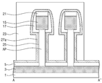
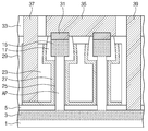
도 16을 참조하면, 게이트 절연막(25)이 열산화 공정에 의해 두껍게 형성될 경우, 활성 기둥(AP)의 표면의 일부가 산화되어 상기 게이트 절연막(25)으로 변하고, 상기 활성 기둥(AP)의 제 3 폭(W3)은 원래의 제 1 폭(W1) 보다 좁아질 수 있다. 도 16의 반도체 장치에서 그 외의 구성은 도 2를 참조하여 설명한 바와 동일/유사할 수 있다.16, when the
도 17을 참조하면, 본 예에 따른 반도체 장치는 고유전막(26)을 더 포함한다. 상기 고유전막(26)은 실리콘 산화막보다 높은 유전율을 가지는 물질로 예를 들면 금속산화막을 포함할 수 있다. 상기 고유전막(26)은 증착 공정으로 형성될 수 있다. 상기 고유전막(26)은 상기 게이트 절연막(26)과 상기 상기 게이트 전극(27) 사이 그리고 스페이서(17)과 상기 게이트 전극(27) 사이에 개재될 수 있다. 상기 고유전막(26)도 게이트 절연막으로서 역할을 하며, 수직 전계 트랜지스터의 문턱전압을 조절하기 위해 사용될 수 있다. 그 외의 구성은 도 2를 참조하여 설명한 바와 동일/유사할 수 있다. Referring to FIG. 17, the semiconductor device according to the present example further includes a high-
도 18을 참조하면, 본 예에 따른 반도체 장치는 도 13의 마스크 패턴(23)을 포함한다. 즉, 도 13의 마스크 패턴(23)을 제거하지 않고 후속 공정을 진행한 경우 형성될 수 있다. 이때에는 상기 마스크 패턴(23)을 제거하는 공정을 줄일 수 있어 공정을 단순화시킬 수 있다. 그 외의 구성은 도 2를 참조하여 설명한 바와 동일/유사할 수 있다. Referring to Fig. 18, the semiconductor device according to this example includes the
1: 반도체 기판
3: 제 1 소오스/드레인부
5, 29, 33: 절연막
7, 9, 11: 희생 절연막
13: 갭 영역
15: 제 2 소오스/드레인부
17: 스페이서
21: 캐핑 패턴
23: 마스크 패턴
25: 게이트 절연막
26: 고유전막
27: 게이트 전극
35: 상부전극
37: 게이트 전극 콘택
39: 하부전극 콘택1: semiconductor substrate
3: first source / drain portion
5, 29, 33: insulating film
7, 9, 11: a sacrificial insulating film
13: gap area
15: second source / drain portion
17: Spacer
21: capping pattern
23: mask pattern
25: Gate insulating film
26: high dielectric constant film
27: gate electrode
35: upper electrode
37: Gate electrode contact
39: Lower electrode contact
Claims (10)
상기 활성 기둥의 상단에 배치되며 상기 활성 기둥보다 넓은 폭을 가지는 제 1 소오스/드레인부;
상기 제 1 소오스/드레인부의 적어도 하부면을 덮는 스페이서;
상기 스페이서의 하부면과 상기 활성 기둥의 측면을 덮는 게이트 전극;
상기 게이트 전극과 상기 활성 기둥 사이에 개재된 게이트 절연막; 및
상기 활성 기둥 아래의 상기 기판 내에 배치되는 제 2 소오스/드레인부를 포함하는 반도체 장치. Active pillars protruding from the substrate;
A first source / drain disposed at an upper end of the active column and having a width greater than that of the active column;
A spacer covering at least the lower surface of the first source / drain portion;
A gate electrode covering a lower surface of the spacer and a side surface of the active column;
A gate insulating film interposed between the gate electrode and the active column; And
And a second source / drain portion disposed in the substrate under the active column.
상기 스페이서는 연장되어 상기 제 1 소오스/드레인부의 측면을 일부 덮는 반도체 장치. The method according to claim 1,
Wherein the spacer extends to partially cover a side surface of the first source / drain portion.
상기 게이트 전극은 연장되어 상기 기판의 일부를 덮으며,
상기 게이트 전극과 상기 기판 사이에 개재되는 제 1 절연막을 더 포함하며,
상기 제 1 절연막은 상기 게이트 절연막보다 두꺼운 반도체 장치. The method according to claim 1,
Wherein the gate electrode extends to cover a portion of the substrate,
And a first insulating film interposed between the gate electrode and the substrate,
Wherein the first insulating film is thicker than the gate insulating film.
상기 제 1 소오스/드레인부의 상부와 전기적으로 연결되는 상부전극을 더 포함하며,
상기 상부전극은 상기 게이트 전극과 이격되는 반도체 장치. The method according to claim 1,
And an upper electrode electrically connected to an upper portion of the first source / drain portion,
And the upper electrode is spaced apart from the gate electrode.
상기 활성 기둥과 상기 제 1 소오스/드레인부는 복수개이며,
상기 상부전극은 복수개의 상기 제 1 소오스/드레인부들과 동시에 연결되는 반도체 장치. 5. The method of claim 4,
Wherein the active pillars and the first source / drain portions are plural,
And the upper electrode is simultaneously connected to the plurality of first source / drain portions.
상기 게이트 절연막은 고유전막을 포함하며,
상기 고유전막은 연장되어 상기 스페이서와 상기 게이트 전극 사이에 개재되는 반도체 장치. The method of claim 1, wherein
Wherein the gate insulating film includes a high dielectric constant film,
Wherein the high-k film is extended and interposed between the spacer and the gate electrode.
상기 활성 기둥은 복수개이며,
상기 게이트 전극은 연장되어 상기 활성 기둥들의 측면들을 덮는 반도체 장치. The method according to claim 1,
The active pillars are plural,
Wherein the gate electrode extends to cover the sides of the active columns.
상기 활성 기둥과 상기 제 1 소오스/드레인부는 복수개이며,
상기 활성 기둥들 사이와 상기 제 1 소오스/드레인부들 사이를 채우며 상기 상부전극의 하부면과 접하는 제 1 층간절연막; 및
상기 제 1 층간절연막을 덮으며 상기 상부전극의 측면과 접하는 제 2 층간절연막을 더 포함하는 반도체 장치. The method according to claim 1,
Wherein the active pillars and the first source / drain portions are plural,
A first interlayer insulating film which fills between the active columns and the first source / drain regions and contacts the lower surface of the upper electrode; And
And a second interlayer insulating film covering the first interlayer insulating film and contacting a side surface of the upper electrode.
상기 활성 기둥 아래의 상기 반도체 기판에 제 1 소오스/드레인부를 형성하는 단계;
상기 반도체 기판 상에 제 1 절연막을 형성하여 상기 활성 기둥을 덮는 단계;
상기 제 1 절연막에 대하여 에치백 공정을 진행하여 상기 활성 기둥의 상부를 노출시키는 단계;
상기 노출된 상기 활성 기둥의 상부에 상기 활성 기둥보다 넓은 폭을 가지되 상기 제 1 절연막과 이격된 제 2 소오스/드레인부를 형성하는 단계;
상기 제 2 소오스/드레인부의 측벽과 하부면을 덮는 스페이서를 형성하는 단계;
상기 제 1 절연막을 제거하여 상기 스페이서의 하부면과 상기 활성 기둥의 측벽을 노출시키는 단계; 및
상기 스페이서의 하부면과 상기 활성 기둥의 측벽을 덮는 게이트 전극을 형성하는 단계를 포함하는 반도체 장치의 제조 방법.Forming an active column protruding from the surface of the semiconductor substrate;
Forming a first source / drain portion on the semiconductor substrate under the active pillars;
Forming a first insulating film on the semiconductor substrate to cover the active column;
Performing an etch-back process on the first insulating film to expose an upper portion of the active column;
Forming a second source / drain portion having a width larger than that of the active column and spaced apart from the first insulating film on the exposed active pillars;
Forming a spacer covering the side wall and the bottom surface of the second source / drain portion;
Removing the first insulating film to expose a lower surface of the spacer and a side wall of the active column; And
And forming a gate electrode covering the lower surface of the spacer and the sidewall of the active column.
상기 제 2 소오스/드레인부를 형성하는 단계는,
상기 노출된 활성 기둥의 상부와 상기 제 1 절연막의 상부면을 콘포말하게 덮는 제 2 절연막을 형성하는 단계;
상기 제 3 절연막을 형성하여 상기 활성 기둥의 측면의 상기 제 2 절연막을 덮되, 상기 활성 기둥 상의 상기 제 2 절연막을 노출시키는 단계;
이방성 식각 공정을 진행하여 상기 제 3 절연막과 상기 활성 기둥 사이의 상기 제 2 절연막을 제거하여 상기 활성기둥의 상부면과 상부 측벽을 노출시키되, 상기 제 1 절연막의 상부면과 접하는 상기 제 2 절연막을 남기는 단계; 및
선택적 에피택시얼 성장 공정을 진행하고 불순물을 도핑하여 상기 노출된 활성 기둥을 상기 제 2 소오스/드레인부로 만드는 단계를 포함하는 반도체 장치의 제조 방법.
10. The method of claim 9,
The forming of the second source / drain portion may include:
Forming a second insulating layer that conformally covers an upper portion of the exposed active column and an upper surface of the first insulating layer;
Forming the third insulating film to cover the second insulating film on a side surface of the active column, and exposing the second insulating film on the active column;
The second insulating film between the third insulating film and the active column is removed to expose the upper surface and the upper sidewall of the active column by conducting an anisotropic etching process and the second insulating film contacting the upper surface of the first insulating film, Leaving; And
And performing a selective epitaxial growth process and doping the impurities to form the exposed active pillars into the second source / drain portion.
Priority Applications (4)
| Application Number | Priority Date | Filing Date | Title |
|---|---|---|---|
| KR1020170024948A KR102773973B1 (en) | 2017-02-24 | 2017-02-24 | Semiconductor device and Method of fabricating the same |
| US15/664,226 US10256324B2 (en) | 2017-02-24 | 2017-07-31 | Semiconductor devices having vertical transistors with aligned gate electrodes |
| CN201810156564.2A CN108511526B (en) | 2017-02-24 | 2018-02-24 | Semiconductor device with vertical transistor with aligned gate electrode and method of manufacturing same |
| US16/284,843 US10559673B2 (en) | 2017-02-24 | 2019-02-25 | Semiconductor devices having vertical transistors with aligned gate electrodes |
Applications Claiming Priority (1)
| Application Number | Priority Date | Filing Date | Title |
|---|---|---|---|
| KR1020170024948A KR102773973B1 (en) | 2017-02-24 | 2017-02-24 | Semiconductor device and Method of fabricating the same |
Publications (2)
| Publication Number | Publication Date |
|---|---|
| KR20180098446A true KR20180098446A (en) | 2018-09-04 |
| KR102773973B1 KR102773973B1 (en) | 2025-03-05 |
Family
ID=63246449
Family Applications (1)
| Application Number | Title | Priority Date | Filing Date |
|---|---|---|---|
| KR1020170024948A Active KR102773973B1 (en) | 2017-02-24 | 2017-02-24 | Semiconductor device and Method of fabricating the same |
Country Status (3)
| Country | Link |
|---|---|
| US (2) | US10256324B2 (en) |
| KR (1) | KR102773973B1 (en) |
| CN (1) | CN108511526B (en) |
Cited By (2)
| Publication number | Priority date | Publication date | Assignee | Title |
|---|---|---|---|---|
| KR20210043414A (en) * | 2019-10-11 | 2021-04-21 | 삼성전자주식회사 | Vertical field-effect transistor(vfet) devices and methods of forming the same |
| KR20210154602A (en) * | 2020-06-12 | 2021-12-21 | 삼성전자주식회사 | Semiconductor device and a method for manufacturing the same |
Families Citing this family (10)
| Publication number | Priority date | Publication date | Assignee | Title |
|---|---|---|---|---|
| KR102273365B1 (en) * | 2017-05-12 | 2021-07-06 | 씨투에이엠피에스 에이비 | Vertical metal oxide semiconductor field effect transistor and method of forming same |
| US10199278B2 (en) * | 2017-05-30 | 2019-02-05 | International Business Machines Corporation | Vertical field effect transistor (FET) with controllable gate length |
| EP3454378A1 (en) * | 2017-09-08 | 2019-03-13 | IMEC vzw | A method for forming a vertical channel device, and a vertical channel device |
| US10297507B2 (en) * | 2017-10-17 | 2019-05-21 | International Business Machines Corporation | Self-aligned vertical field-effect transistor with epitaxially grown bottom and top source drain regions |
| US10672887B2 (en) * | 2017-12-12 | 2020-06-02 | International Business Machines Corporation | Vertical FET with shaped spacer to reduce parasitic capacitance |
| US10535754B2 (en) * | 2018-06-05 | 2020-01-14 | International Business Machines Corporation | Method and structure for forming a vertical field-effect transistor |
| US11640987B2 (en) * | 2021-02-04 | 2023-05-02 | Applied Materials, Inc. | Implant to form vertical FETs with self-aligned drain spacer and junction |
| US12369295B2 (en) | 2022-04-26 | 2025-07-22 | Changxin Memory Technologies, Inc. | Semiconductor structure and manufacturing method thereof |
| US12414285B2 (en) | 2022-04-26 | 2025-09-09 | Changxin Memory Technologies, Inc. | Semiconductor structure and manufacturing method thereof |
| US12342524B2 (en) * | 2022-04-26 | 2025-06-24 | Changxin Memory Technologies, Inc. | Method for fabricating semiconductor device and semiconductor device |
Citations (5)
| Publication number | Priority date | Publication date | Assignee | Title |
|---|---|---|---|---|
| KR20030058633A (en) * | 2001-12-31 | 2003-07-07 | 주식회사 하이닉스반도체 | Vertical transistor and method of manufacturing the same |
| KR20140030019A (en) * | 2012-08-30 | 2014-03-11 | 타이완 세미콘덕터 매뉴팩쳐링 컴퍼니 리미티드 | System and method for a field-effect transistor with a raised drain structure |
| KR20160123972A (en) * | 2015-04-17 | 2016-10-26 | 타이완 세미콘덕터 매뉴팩쳐링 컴퍼니 리미티드 | Two-port sram cell structure with vertical devices |
| US20170243974A1 (en) * | 2016-01-28 | 2017-08-24 | International Business Machines Corporation | Vertical field effect transistors with protective fin liner during bottom spacer recess etch |
| US20180076093A1 (en) * | 2016-09-12 | 2018-03-15 | International Business Machines Corporation | Vertical transistors having different gate lengths |
Family Cites Families (23)
| Publication number | Priority date | Publication date | Assignee | Title |
|---|---|---|---|---|
| CN1157480A (en) * | 1995-08-30 | 1997-08-20 | 摩托罗拉公司 | Method for forming unilateral slowly-varying channel semiconductor device with gate electrode easy-to-handle spacer |
| KR100660881B1 (en) * | 2005-10-12 | 2006-12-26 | 삼성전자주식회사 | Semiconductor device with vertical channel transistor and manufacturing method thereof |
| US20070148939A1 (en) | 2005-12-22 | 2007-06-28 | International Business Machines Corporation | Low leakage heterojunction vertical transistors and high performance devices thereof |
| KR100725370B1 (en) * | 2006-01-05 | 2007-06-07 | 삼성전자주식회사 | Method of manufacturing semiconductor device and semiconductor device manufactured thereby |
| KR100734313B1 (en) * | 2006-02-09 | 2007-07-02 | 삼성전자주식회사 | Semiconductor device having vertical channel and manufacturing method thereof |
| JP5317343B2 (en) | 2009-04-28 | 2013-10-16 | ユニサンティス エレクトロニクス シンガポール プライベート リミテッド | Semiconductor device and manufacturing method thereof |
| KR100971411B1 (en) | 2008-05-21 | 2010-07-21 | 주식회사 하이닉스반도체 | Method of forming vertical channel transistor in semiconductor device |
| CN102709190B (en) * | 2012-05-24 | 2017-04-26 | 上海华虹宏力半导体制造有限公司 | LDMOS (Laterally Diffused Metal Oxide Semiconductor) field effect transistor and manufacturing method thereof |
| FR2991100B1 (en) | 2012-05-25 | 2014-06-27 | Commissariat Energie Atomique | NANOFIL-BASED TRANSISTOR, PROCESS FOR PRODUCING THE TRANSISTOR, SEMICONDUCTOR COMPONENT INTEGRATING THE TRANSISTOR, COMPUTER PROGRAM, AND RECORDING MEDIUM ASSOCIATED WITH THE MANUFACTURING METHOD |
| US8969963B2 (en) * | 2012-10-12 | 2015-03-03 | International Business Machines Corporation | Vertical source/drain junctions for a finFET including a plurality of fins |
| JP2014135359A (en) | 2013-01-09 | 2014-07-24 | Tokyo Institute Of Technology | Field-effect transistor |
| US10276664B2 (en) * | 2014-02-10 | 2019-04-30 | Taiwan Semiconductor Manufacturing Company Limited | Semiconductor structures and methods for multi-dimension of nanowire diameter to improve drive current |
| JP6287473B2 (en) * | 2014-03-28 | 2018-03-07 | Tdk株式会社 | Bridgeless power factor correction converter |
| US9755033B2 (en) * | 2014-06-13 | 2017-09-05 | Taiwan Semiconductor Manufacturing Co., Ltd. | Semiconductor device and method of forming vertical structure |
| US9698261B2 (en) * | 2014-06-30 | 2017-07-04 | Taiwan Semiconductor Manufacturing Co., Ltd. | Vertical device architecture |
| US9406793B2 (en) * | 2014-07-03 | 2016-08-02 | Broadcom Corporation | Semiconductor device with a vertical channel formed through a plurality of semiconductor layers |
| US9911848B2 (en) * | 2014-08-29 | 2018-03-06 | Taiwan Semiconductor Manufacturing Co., Ltd. | Vertical transistor and method of manufacturing the same |
| CN104218089B (en) * | 2014-09-10 | 2017-02-15 | 北京大学 | Stepped gate-dielectric double-layer graphene field effect transistor and production method thereof |
| US9373620B2 (en) * | 2014-09-12 | 2016-06-21 | Taiwan Semiconductor Manufacturing Co., Ltd. | Series connected transistor structure and method of manufacturing the same |
| TWI662625B (en) * | 2015-01-19 | 2019-06-11 | 聯華電子股份有限公司 | Semiconductor device and method for fabricating the same |
| US9349860B1 (en) | 2015-03-31 | 2016-05-24 | Taiwan Semiconductor Manufacturing Company, Ltd. | Field effect transistors and methods of forming same |
| US20160336324A1 (en) * | 2015-05-15 | 2016-11-17 | Qualcomm Incorporated | Tunnel field effect transistor and method of making the same |
| US10170616B2 (en) * | 2016-09-19 | 2019-01-01 | Globalfoundries Inc. | Methods of forming a vertical transistor device |
-
2017
- 2017-02-24 KR KR1020170024948A patent/KR102773973B1/en active Active
- 2017-07-31 US US15/664,226 patent/US10256324B2/en active Active
-
2018
- 2018-02-24 CN CN201810156564.2A patent/CN108511526B/en active Active
-
2019
- 2019-02-25 US US16/284,843 patent/US10559673B2/en active Active
Patent Citations (5)
| Publication number | Priority date | Publication date | Assignee | Title |
|---|---|---|---|---|
| KR20030058633A (en) * | 2001-12-31 | 2003-07-07 | 주식회사 하이닉스반도체 | Vertical transistor and method of manufacturing the same |
| KR20140030019A (en) * | 2012-08-30 | 2014-03-11 | 타이완 세미콘덕터 매뉴팩쳐링 컴퍼니 리미티드 | System and method for a field-effect transistor with a raised drain structure |
| KR20160123972A (en) * | 2015-04-17 | 2016-10-26 | 타이완 세미콘덕터 매뉴팩쳐링 컴퍼니 리미티드 | Two-port sram cell structure with vertical devices |
| US20170243974A1 (en) * | 2016-01-28 | 2017-08-24 | International Business Machines Corporation | Vertical field effect transistors with protective fin liner during bottom spacer recess etch |
| US20180076093A1 (en) * | 2016-09-12 | 2018-03-15 | International Business Machines Corporation | Vertical transistors having different gate lengths |
Cited By (2)
| Publication number | Priority date | Publication date | Assignee | Title |
|---|---|---|---|---|
| KR20210043414A (en) * | 2019-10-11 | 2021-04-21 | 삼성전자주식회사 | Vertical field-effect transistor(vfet) devices and methods of forming the same |
| KR20210154602A (en) * | 2020-06-12 | 2021-12-21 | 삼성전자주식회사 | Semiconductor device and a method for manufacturing the same |
Also Published As
| Publication number | Publication date |
|---|---|
| KR102773973B1 (en) | 2025-03-05 |
| US10559673B2 (en) | 2020-02-11 |
| US20190189778A1 (en) | 2019-06-20 |
| CN108511526B (en) | 2024-01-02 |
| US10256324B2 (en) | 2019-04-09 |
| US20180248018A1 (en) | 2018-08-30 |
| CN108511526A (en) | 2018-09-07 |
Similar Documents
| Publication | Publication Date | Title |
|---|---|---|
| KR102773973B1 (en) | Semiconductor device and Method of fabricating the same | |
| US9590038B1 (en) | Semiconductor device having nanowire channel | |
| US11710736B2 (en) | Semiconductor device and method of manufacturing the same | |
| KR102593561B1 (en) | Semiconductor device | |
| US8129777B2 (en) | Semiconductor device having a multi-channel type MOS transistor | |
| KR101882360B1 (en) | Semiconductor device including buried gate structure and method of manufacturing the same | |
| GB2395603A (en) | Multichannel TFT having gate formed around channels | |
| US10050114B2 (en) | Semiconductor device and method of manufacturing the same | |
| US10332898B2 (en) | Semiconductor device and method of manufacturing the same | |
| CN101017825A (en) | Semiconductor device having vertical channel and method of manufacturing the same | |
| KR102363250B1 (en) | Semiconductor device | |
| KR20190029942A (en) | Semiconductor devices having a vertical channel and method of manufacturing the same | |
| US10192966B2 (en) | Semiconductor devices including recessed gate electrode portions | |
| KR20170137637A (en) | Semiconductor device and manufacturing method of the same | |
| KR102755165B1 (en) | Semiconductor device | |
| US12249648B2 (en) | Semiconductor device having spacer between contract patterns | |
| US20170033217A1 (en) | Semiconductor devices and methods of manufacturing the same | |
| US12389688B2 (en) | Semiconductor device having dielectric layers of varying thicknesses | |
| KR20230062467A (en) | Semiconductor structure and manufacturing method thereof | |
| CN110718548B (en) | Semiconductor Devices | |
| KR102568718B1 (en) | Semiconductor devices | |
| KR102907655B1 (en) | Semiconductor device having upper channels and lower channels and method of manufacturing the same | |
| KR102667811B1 (en) | Semiconductor device | |
| KR102845847B1 (en) | Semiconductor device | |
| TW202040697A (en) | A method for forming a semiconductor device |
Legal Events
| Date | Code | Title | Description |
|---|---|---|---|
| PA0109 | Patent application |
Patent event code: PA01091R01D Comment text: Patent Application Patent event date: 20170224 |
|
| PG1501 | Laying open of application | ||
| A201 | Request for examination | ||
| PA0201 | Request for examination |
Patent event code: PA02012R01D Patent event date: 20220224 Comment text: Request for Examination of Application Patent event code: PA02011R01I Patent event date: 20170224 Comment text: Patent Application |
|
| E902 | Notification of reason for refusal | ||
| PE0902 | Notice of grounds for rejection |
Comment text: Notification of reason for refusal Patent event date: 20240411 Patent event code: PE09021S01D |
|
| E701 | Decision to grant or registration of patent right | ||
| PE0701 | Decision of registration |
Patent event code: PE07011S01D Comment text: Decision to Grant Registration Patent event date: 20241202 |
|
| GRNT | Written decision to grant | ||
| PR0701 | Registration of establishment |
Comment text: Registration of Establishment Patent event date: 20250224 Patent event code: PR07011E01D |
|
| PR1002 | Payment of registration fee |
Payment date: 20250225 End annual number: 3 Start annual number: 1 |
|
| PG1601 | Publication of registration |