US7723016B2 - Method for forming resist pattern and method for manufacturing a semiconductor device - Google Patents
Method for forming resist pattern and method for manufacturing a semiconductor device Download PDFInfo
- Publication number
- US7723016B2 US7723016B2 US12/292,170 US29217008A US7723016B2 US 7723016 B2 US7723016 B2 US 7723016B2 US 29217008 A US29217008 A US 29217008A US 7723016 B2 US7723016 B2 US 7723016B2
- Authority
- US
- United States
- Prior art keywords
- resist
- resist pattern
- pattern
- film
- wavelength
- Prior art date
- Legal status (The legal status is an assumption and is not a legal conclusion. Google has not performed a legal analysis and makes no representation as to the accuracy of the status listed.)
- Expired - Lifetime
Links
- 238000000034 method Methods 0.000 title claims abstract description 80
- 238000004519 manufacturing process Methods 0.000 title claims abstract description 72
- 239000004065 semiconductor Substances 0.000 title claims abstract description 53
- 239000000463 material Substances 0.000 claims abstract description 109
- 239000002253 acid Substances 0.000 claims abstract description 54
- 238000000059 patterning Methods 0.000 claims abstract description 17
- 238000010521 absorption reaction Methods 0.000 claims abstract description 11
- 238000005530 etching Methods 0.000 claims abstract description 9
- 239000002245 particle Substances 0.000 claims description 12
- 230000001747 exhibiting effect Effects 0.000 claims 4
- 238000000576 coating method Methods 0.000 abstract description 8
- 239000011248 coating agent Substances 0.000 abstract description 7
- 239000010408 film Substances 0.000 description 137
- 239000010410 layer Substances 0.000 description 58
- 229920005989 resin Polymers 0.000 description 29
- 239000011347 resin Substances 0.000 description 29
- 229910021420 polycrystalline silicon Inorganic materials 0.000 description 24
- 229920005591 polysilicon Polymers 0.000 description 24
- 238000009413 insulation Methods 0.000 description 23
- VYPSYNLAJGMNEJ-UHFFFAOYSA-N Silicium dioxide Chemical compound O=[Si]=O VYPSYNLAJGMNEJ-UHFFFAOYSA-N 0.000 description 21
- 230000008569 process Effects 0.000 description 21
- 239000004020 conductor Substances 0.000 description 20
- 230000015654 memory Effects 0.000 description 18
- 239000000758 substrate Substances 0.000 description 18
- 230000002093 peripheral effect Effects 0.000 description 15
- 239000002904 solvent Substances 0.000 description 15
- WGTYBPLFGIVFAS-UHFFFAOYSA-M tetramethylammonium hydroxide Chemical compound [OH-].C[N+](C)(C)C WGTYBPLFGIVFAS-UHFFFAOYSA-M 0.000 description 12
- 239000003990 capacitor Substances 0.000 description 11
- -1 salt compound Chemical class 0.000 description 11
- 229910052681 coesite Inorganic materials 0.000 description 10
- 229910052906 cristobalite Inorganic materials 0.000 description 10
- 239000012528 membrane Substances 0.000 description 10
- 125000006239 protecting group Chemical group 0.000 description 10
- 239000000377 silicon dioxide Substances 0.000 description 10
- 229910052682 stishovite Inorganic materials 0.000 description 10
- 239000000126 substance Substances 0.000 description 10
- 229910052905 tridymite Inorganic materials 0.000 description 10
- 239000007864 aqueous solution Substances 0.000 description 9
- 125000003178 carboxy group Chemical group [H]OC(*)=O 0.000 description 9
- 229920001577 copolymer Polymers 0.000 description 9
- 230000008018 melting Effects 0.000 description 9
- 238000002844 melting Methods 0.000 description 9
- 238000006243 chemical reaction Methods 0.000 description 8
- 238000007667 floating Methods 0.000 description 8
- 150000002596 lactones Chemical group 0.000 description 8
- 229920000642 polymer Polymers 0.000 description 8
- 239000010409 thin film Substances 0.000 description 8
- 239000003513 alkali Substances 0.000 description 7
- 150000001875 compounds Chemical class 0.000 description 7
- 239000003431 cross linking reagent Substances 0.000 description 7
- 230000008719 thickening Effects 0.000 description 7
- 125000000524 functional group Chemical group 0.000 description 6
- 239000011229 interlayer Substances 0.000 description 6
- 230000005855 radiation Effects 0.000 description 6
- 238000004528 spin coating Methods 0.000 description 6
- 125000001424 substituent group Chemical group 0.000 description 6
- 230000015572 biosynthetic process Effects 0.000 description 5
- 239000012535 impurity Substances 0.000 description 5
- 229920002120 photoresistant polymer Polymers 0.000 description 5
- 239000010936 titanium Substances 0.000 description 5
- OAICVXFJPJFONN-UHFFFAOYSA-N Phosphorus Chemical compound [P] OAICVXFJPJFONN-UHFFFAOYSA-N 0.000 description 4
- 125000005073 adamantyl group Chemical group C12(CC3CC(CC(C1)C3)C2)* 0.000 description 4
- 229910052785 arsenic Inorganic materials 0.000 description 4
- RQNWIZPPADIBDY-UHFFFAOYSA-N arsenic atom Chemical compound [As] RQNWIZPPADIBDY-UHFFFAOYSA-N 0.000 description 4
- 238000010276 construction Methods 0.000 description 4
- 238000004132 cross linking Methods 0.000 description 4
- 238000004090 dissolution Methods 0.000 description 4
- LZCLXQDLBQLTDK-UHFFFAOYSA-N ethyl 2-hydroxypropanoate Chemical compound CCOC(=O)C(C)O LZCLXQDLBQLTDK-UHFFFAOYSA-N 0.000 description 4
- 238000007747 plating Methods 0.000 description 4
- 229920001665 Poly-4-vinylphenol Polymers 0.000 description 3
- 230000009471 action Effects 0.000 description 3
- 238000011161 development Methods 0.000 description 3
- 238000010894 electron beam technology Methods 0.000 description 3
- 238000000609 electron-beam lithography Methods 0.000 description 3
- 238000005516 engineering process Methods 0.000 description 3
- 238000003475 lamination Methods 0.000 description 3
- 238000001459 lithography Methods 0.000 description 3
- 230000007246 mechanism Effects 0.000 description 3
- 230000003647 oxidation Effects 0.000 description 3
- 238000007254 oxidation reaction Methods 0.000 description 3
- 238000002360 preparation method Methods 0.000 description 3
- LLHKCFNBLRBOGN-UHFFFAOYSA-N propylene glycol methyl ether acetate Chemical compound COCC(C)OC(C)=O LLHKCFNBLRBOGN-UHFFFAOYSA-N 0.000 description 3
- 230000004044 response Effects 0.000 description 3
- 230000035945 sensitivity Effects 0.000 description 3
- ARXJGSRGQADJSQ-UHFFFAOYSA-N 1-methoxypropan-2-ol Chemical compound COCC(C)O ARXJGSRGQADJSQ-UHFFFAOYSA-N 0.000 description 2
- JESXATFQYMPTNL-UHFFFAOYSA-N 2-ethenylphenol Chemical compound OC1=CC=CC=C1C=C JESXATFQYMPTNL-UHFFFAOYSA-N 0.000 description 2
- YEJRWHAVMIAJKC-UHFFFAOYSA-N 4-Butyrolactone Chemical compound O=C1CCCO1 YEJRWHAVMIAJKC-UHFFFAOYSA-N 0.000 description 2
- VZCYOOQTPOCHFL-OWOJBTEDSA-N Fumaric acid Chemical compound OC(=O)\C=C\C(O)=O VZCYOOQTPOCHFL-OWOJBTEDSA-N 0.000 description 2
- 229910003271 Ni-Fe Inorganic materials 0.000 description 2
- XUIMIQQOPSSXEZ-UHFFFAOYSA-N Silicon Chemical compound [Si] XUIMIQQOPSSXEZ-UHFFFAOYSA-N 0.000 description 2
- PPBRXRYQALVLMV-UHFFFAOYSA-N Styrene Chemical compound C=CC1=CC=CC=C1 PPBRXRYQALVLMV-UHFFFAOYSA-N 0.000 description 2
- 229920001807 Urea-formaldehyde Polymers 0.000 description 2
- 238000002835 absorbance Methods 0.000 description 2
- 229920006222 acrylic ester polymer Polymers 0.000 description 2
- 239000000654 additive Substances 0.000 description 2
- 125000002723 alicyclic group Chemical group 0.000 description 2
- 125000003545 alkoxy group Chemical group 0.000 description 2
- 239000002585 base Substances 0.000 description 2
- 150000001768 cations Chemical class 0.000 description 2
- OZLBDYMWFAHSOQ-UHFFFAOYSA-N diphenyliodanium Chemical compound C=1C=CC=CC=1[I+]C1=CC=CC=C1 OZLBDYMWFAHSOQ-UHFFFAOYSA-N 0.000 description 2
- 229940116333 ethyl lactate Drugs 0.000 description 2
- 229910052739 hydrogen Inorganic materials 0.000 description 2
- 230000002209 hydrophobic effect Effects 0.000 description 2
- YAMHXTCMCPHKLN-UHFFFAOYSA-N imidazolidin-2-one Chemical compound O=C1NCCN1 YAMHXTCMCPHKLN-UHFFFAOYSA-N 0.000 description 2
- 238000005468 ion implantation Methods 0.000 description 2
- 239000004973 liquid crystal related substance Substances 0.000 description 2
- 150000007974 melamines Chemical class 0.000 description 2
- QSHDDOUJBYECFT-UHFFFAOYSA-N mercury Chemical compound [Hg] QSHDDOUJBYECFT-UHFFFAOYSA-N 0.000 description 2
- BDJSOPWXYLFTNW-UHFFFAOYSA-N methyl 3-methoxypropanoate Chemical compound COCCC(=O)OC BDJSOPWXYLFTNW-UHFFFAOYSA-N 0.000 description 2
- 230000003287 optical effect Effects 0.000 description 2
- 229910000889 permalloy Inorganic materials 0.000 description 2
- 125000002924 primary amino group Chemical group [H]N([H])* 0.000 description 2
- 150000003839 salts Chemical class 0.000 description 2
- 229910052710 silicon Inorganic materials 0.000 description 2
- 239000010703 silicon Substances 0.000 description 2
- 238000004544 sputter deposition Methods 0.000 description 2
- 238000010897 surface acoustic wave method Methods 0.000 description 2
- 239000002344 surface layer Substances 0.000 description 2
- 150000003672 ureas Chemical class 0.000 description 2
- XLYOFNOQVPJJNP-UHFFFAOYSA-N water Substances O XLYOFNOQVPJJNP-UHFFFAOYSA-N 0.000 description 2
- SJHPCNCNNSSLPL-CSKARUKUSA-N (4e)-4-(ethoxymethylidene)-2-phenyl-1,3-oxazol-5-one Chemical compound O1C(=O)C(=C/OCC)\N=C1C1=CC=CC=C1 SJHPCNCNNSSLPL-CSKARUKUSA-N 0.000 description 1
- JAHNSTQSQJOJLO-UHFFFAOYSA-N 2-(3-fluorophenyl)-1h-imidazole Chemical compound FC1=CC=CC(C=2NC=CN=2)=C1 JAHNSTQSQJOJLO-UHFFFAOYSA-N 0.000 description 1
- XUDBVJCTLZTSDC-UHFFFAOYSA-N 2-ethenylbenzoic acid Chemical compound OC(=O)C1=CC=CC=C1C=C XUDBVJCTLZTSDC-UHFFFAOYSA-N 0.000 description 1
- RHLVCLIPMVJYKS-UHFFFAOYSA-N 3-octanone Chemical compound CCCCCC(=O)CC RHLVCLIPMVJYKS-UHFFFAOYSA-N 0.000 description 1
- GZVHEAJQGPRDLQ-UHFFFAOYSA-N 6-phenyl-1,3,5-triazine-2,4-diamine Chemical compound NC1=NC(N)=NC(C=2C=CC=CC=2)=N1 GZVHEAJQGPRDLQ-UHFFFAOYSA-N 0.000 description 1
- DKPFZGUDAPQIHT-UHFFFAOYSA-N Butyl acetate Natural products CCCCOC(C)=O DKPFZGUDAPQIHT-UHFFFAOYSA-N 0.000 description 1
- 229920000089 Cyclic olefin copolymer Polymers 0.000 description 1
- 229920000877 Melamine resin Polymers 0.000 description 1
- SECXISVLQFMRJM-UHFFFAOYSA-N N-Methylpyrrolidone Chemical compound CN1CCCC1=O SECXISVLQFMRJM-UHFFFAOYSA-N 0.000 description 1
- 229910052581 Si3N4 Inorganic materials 0.000 description 1
- DHXVGJBLRPWPCS-UHFFFAOYSA-N Tetrahydropyran Chemical group C1CCOCC1 DHXVGJBLRPWPCS-UHFFFAOYSA-N 0.000 description 1
- RTAQQCXQSZGOHL-UHFFFAOYSA-N Titanium Chemical compound [Ti] RTAQQCXQSZGOHL-UHFFFAOYSA-N 0.000 description 1
- XSQUKJJJFZCRTK-UHFFFAOYSA-N Urea Chemical compound NC(N)=O XSQUKJJJFZCRTK-UHFFFAOYSA-N 0.000 description 1
- UGACIEPFGXRWCH-UHFFFAOYSA-N [Si].[Ti] Chemical compound [Si].[Ti] UGACIEPFGXRWCH-UHFFFAOYSA-N 0.000 description 1
- 238000009825 accumulation Methods 0.000 description 1
- 150000007513 acids Chemical class 0.000 description 1
- 230000000996 additive effect Effects 0.000 description 1
- 125000000217 alkyl group Chemical group 0.000 description 1
- 150000001450 anions Chemical class 0.000 description 1
- 150000001491 aromatic compounds Chemical class 0.000 description 1
- LKXGYGYFPTZHLC-UHFFFAOYSA-N bicyclo[2.2.1]heptane-4-carboxylic acid Chemical compound C1CC2CCC1(C(=O)O)C2 LKXGYGYFPTZHLC-UHFFFAOYSA-N 0.000 description 1
- 239000004202 carbamide Substances 0.000 description 1
- 125000004432 carbon atom Chemical group C* 0.000 description 1
- 230000003197 catalytic effect Effects 0.000 description 1
- 238000006555 catalytic reaction Methods 0.000 description 1
- 239000000919 ceramic Substances 0.000 description 1
- 230000008859 change Effects 0.000 description 1
- 239000003795 chemical substances by application Substances 0.000 description 1
- 239000002131 composite material Substances 0.000 description 1
- 229910052802 copper Inorganic materials 0.000 description 1
- 125000006165 cyclic alkyl group Chemical group 0.000 description 1
- 125000004122 cyclic group Chemical group 0.000 description 1
- 238000010494 dissociation reaction Methods 0.000 description 1
- 230000005593 dissociations Effects 0.000 description 1
- 238000001312 dry etching Methods 0.000 description 1
- 230000000694 effects Effects 0.000 description 1
- 230000008030 elimination Effects 0.000 description 1
- 238000003379 elimination reaction Methods 0.000 description 1
- BHXIWUJLHYHGSJ-UHFFFAOYSA-N ethyl 3-ethoxypropanoate Chemical compound CCOCCC(=O)OCC BHXIWUJLHYHGSJ-UHFFFAOYSA-N 0.000 description 1
- 230000008020 evaporation Effects 0.000 description 1
- 238000001704 evaporation Methods 0.000 description 1
- 239000001530 fumaric acid Substances 0.000 description 1
- 230000006870 function Effects 0.000 description 1
- 125000005843 halogen group Chemical group 0.000 description 1
- CATSNJVOTSVZJV-UHFFFAOYSA-N heptan-2-one Chemical compound CCCCCC(C)=O CATSNJVOTSVZJV-UHFFFAOYSA-N 0.000 description 1
- PYGSKMBEVAICCR-UHFFFAOYSA-N hexa-1,5-diene Chemical group C=CCCC=C PYGSKMBEVAICCR-UHFFFAOYSA-N 0.000 description 1
- FUZZWVXGSFPDMH-UHFFFAOYSA-N hexanoic acid Chemical compound CCCCCC(O)=O FUZZWVXGSFPDMH-UHFFFAOYSA-N 0.000 description 1
- 125000004435 hydrogen atom Chemical group [H]* 0.000 description 1
- 230000006872 improvement Effects 0.000 description 1
- 239000012212 insulator Substances 0.000 description 1
- 238000010884 ion-beam technique Methods 0.000 description 1
- 150000002500 ions Chemical class 0.000 description 1
- JDSHMPZPIAZGSV-UHFFFAOYSA-N melamine Chemical compound NC1=NC(N)=NC(N)=N1 JDSHMPZPIAZGSV-UHFFFAOYSA-N 0.000 description 1
- 229910052751 metal Inorganic materials 0.000 description 1
- 239000002184 metal Substances 0.000 description 1
- LVHBHZANLOWSRM-UHFFFAOYSA-N methylenebutanedioic acid Natural products OC(=O)CC(=C)C(O)=O LVHBHZANLOWSRM-UHFFFAOYSA-N 0.000 description 1
- 125000000325 methylidene group Chemical group [H]C([H])=* 0.000 description 1
- 239000000178 monomer Substances 0.000 description 1
- UMRZSTCPUPJPOJ-KNVOCYPGSA-N norbornane Chemical group C1C[C@H]2CC[C@@H]1C2 UMRZSTCPUPJPOJ-KNVOCYPGSA-N 0.000 description 1
- 239000003960 organic solvent Substances 0.000 description 1
- 238000006116 polymerization reaction Methods 0.000 description 1
- 238000006862 quantum yield reaction Methods 0.000 description 1
- 238000011160 research Methods 0.000 description 1
- 238000012827 research and development Methods 0.000 description 1
- 230000027756 respiratory electron transport chain Effects 0.000 description 1
- 229910021332 silicide Inorganic materials 0.000 description 1
- FVBUAEGBCNSCDD-UHFFFAOYSA-N silicide(4-) Chemical compound [Si-4] FVBUAEGBCNSCDD-UHFFFAOYSA-N 0.000 description 1
- 229910052814 silicon oxide Inorganic materials 0.000 description 1
- 238000006467 substitution reaction Methods 0.000 description 1
- 125000000999 tert-butyl group Chemical group [H]C([H])([H])C(*)(C([H])([H])[H])C([H])([H])[H] 0.000 description 1
- ISXSCDLOGDJUNJ-UHFFFAOYSA-N tert-butyl prop-2-enoate Chemical compound CC(C)(C)OC(=O)C=C ISXSCDLOGDJUNJ-UHFFFAOYSA-N 0.000 description 1
- 229920001187 thermosetting polymer Polymers 0.000 description 1
- 229910052719 titanium Inorganic materials 0.000 description 1
- VZCYOOQTPOCHFL-UHFFFAOYSA-N trans-butenedioic acid Natural products OC(=O)C=CC(O)=O VZCYOOQTPOCHFL-UHFFFAOYSA-N 0.000 description 1
- WLOQLWBIJZDHET-UHFFFAOYSA-N triphenylsulfonium Chemical compound C1=CC=CC=C1[S+](C=1C=CC=CC=1)C1=CC=CC=C1 WLOQLWBIJZDHET-UHFFFAOYSA-N 0.000 description 1
- WFKWXMTUELFFGS-UHFFFAOYSA-N tungsten Chemical compound [W] WFKWXMTUELFFGS-UHFFFAOYSA-N 0.000 description 1
- 229910052721 tungsten Inorganic materials 0.000 description 1
- 239000010937 tungsten Substances 0.000 description 1
- 238000001771 vacuum deposition Methods 0.000 description 1
Images


Classifications
-
- G—PHYSICS
- G03—PHOTOGRAPHY; CINEMATOGRAPHY; ANALOGOUS TECHNIQUES USING WAVES OTHER THAN OPTICAL WAVES; ELECTROGRAPHY; HOLOGRAPHY
- G03F—PHOTOMECHANICAL PRODUCTION OF TEXTURED OR PATTERNED SURFACES, e.g. FOR PRINTING, FOR PROCESSING OF SEMICONDUCTOR DEVICES; MATERIALS THEREFOR; ORIGINALS THEREFOR; APPARATUS SPECIALLY ADAPTED THEREFOR
- G03F7/00—Photomechanical, e.g. photolithographic, production of textured or patterned surfaces, e.g. printing surfaces; Materials therefor, e.g. comprising photoresists; Apparatus specially adapted therefor
- G03F7/004—Photosensitive materials
- G03F7/039—Macromolecular compounds which are photodegradable, e.g. positive electron resists
- G03F7/0392—Macromolecular compounds which are photodegradable, e.g. positive electron resists the macromolecular compound being present in a chemically amplified positive photoresist composition
- G03F7/0397—Macromolecular compounds which are photodegradable, e.g. positive electron resists the macromolecular compound being present in a chemically amplified positive photoresist composition the macromolecular compound having an alicyclic moiety in a side chain
-
- G—PHYSICS
- G03—PHOTOGRAPHY; CINEMATOGRAPHY; ANALOGOUS TECHNIQUES USING WAVES OTHER THAN OPTICAL WAVES; ELECTROGRAPHY; HOLOGRAPHY
- G03F—PHOTOMECHANICAL PRODUCTION OF TEXTURED OR PATTERNED SURFACES, e.g. FOR PRINTING, FOR PROCESSING OF SEMICONDUCTOR DEVICES; MATERIALS THEREFOR; ORIGINALS THEREFOR; APPARATUS SPECIALLY ADAPTED THEREFOR
- G03F7/00—Photomechanical, e.g. photolithographic, production of textured or patterned surfaces, e.g. printing surfaces; Materials therefor, e.g. comprising photoresists; Apparatus specially adapted therefor
- G03F7/004—Photosensitive materials
- G03F7/0045—Photosensitive materials with organic non-macromolecular light-sensitive compounds not otherwise provided for, e.g. dissolution inhibitors
-
- Y—GENERAL TAGGING OF NEW TECHNOLOGICAL DEVELOPMENTS; GENERAL TAGGING OF CROSS-SECTIONAL TECHNOLOGIES SPANNING OVER SEVERAL SECTIONS OF THE IPC; TECHNICAL SUBJECTS COVERED BY FORMER USPC CROSS-REFERENCE ART COLLECTIONS [XRACs] AND DIGESTS
- Y10—TECHNICAL SUBJECTS COVERED BY FORMER USPC
- Y10S—TECHNICAL SUBJECTS COVERED BY FORMER USPC CROSS-REFERENCE ART COLLECTIONS [XRACs] AND DIGESTS
- Y10S430/00—Radiation imagery chemistry: process, composition, or product thereof
- Y10S430/1053—Imaging affecting physical property or radiation sensitive material, or producing nonplanar or printing surface - process, composition, or product: radiation sensitive composition or product or process of making binder containing
- Y10S430/1055—Radiation sensitive composition or product or process of making
- Y10S430/114—Initiator containing
- Y10S430/115—Cationic or anionic
-
- Y—GENERAL TAGGING OF NEW TECHNOLOGICAL DEVELOPMENTS; GENERAL TAGGING OF CROSS-SECTIONAL TECHNOLOGIES SPANNING OVER SEVERAL SECTIONS OF THE IPC; TECHNICAL SUBJECTS COVERED BY FORMER USPC CROSS-REFERENCE ART COLLECTIONS [XRACs] AND DIGESTS
- Y10—TECHNICAL SUBJECTS COVERED BY FORMER USPC
- Y10S—TECHNICAL SUBJECTS COVERED BY FORMER USPC CROSS-REFERENCE ART COLLECTIONS [XRACs] AND DIGESTS
- Y10S430/00—Radiation imagery chemistry: process, composition, or product thereof
- Y10S430/1053—Imaging affecting physical property or radiation sensitive material, or producing nonplanar or printing surface - process, composition, or product: radiation sensitive composition or product or process of making binder containing
- Y10S430/1055—Radiation sensitive composition or product or process of making
- Y10S430/114—Initiator containing
- Y10S430/12—Nitrogen compound containing
- Y10S430/121—Nitrogen in heterocyclic ring
-
- Y—GENERAL TAGGING OF NEW TECHNOLOGICAL DEVELOPMENTS; GENERAL TAGGING OF CROSS-SECTIONAL TECHNOLOGIES SPANNING OVER SEVERAL SECTIONS OF THE IPC; TECHNICAL SUBJECTS COVERED BY FORMER USPC CROSS-REFERENCE ART COLLECTIONS [XRACs] AND DIGESTS
- Y10—TECHNICAL SUBJECTS COVERED BY FORMER USPC
- Y10S—TECHNICAL SUBJECTS COVERED BY FORMER USPC CROSS-REFERENCE ART COLLECTIONS [XRACs] AND DIGESTS
- Y10S430/00—Radiation imagery chemistry: process, composition, or product thereof
- Y10S430/1053—Imaging affecting physical property or radiation sensitive material, or producing nonplanar or printing surface - process, composition, or product: radiation sensitive composition or product or process of making binder containing
- Y10S430/1055—Radiation sensitive composition or product or process of making
- Y10S430/114—Initiator containing
- Y10S430/122—Sulfur compound containing
-
- Y—GENERAL TAGGING OF NEW TECHNOLOGICAL DEVELOPMENTS; GENERAL TAGGING OF CROSS-SECTIONAL TECHNOLOGIES SPANNING OVER SEVERAL SECTIONS OF THE IPC; TECHNICAL SUBJECTS COVERED BY FORMER USPC CROSS-REFERENCE ART COLLECTIONS [XRACs] AND DIGESTS
- Y10—TECHNICAL SUBJECTS COVERED BY FORMER USPC
- Y10S—TECHNICAL SUBJECTS COVERED BY FORMER USPC CROSS-REFERENCE ART COLLECTIONS [XRACs] AND DIGESTS
- Y10S430/00—Radiation imagery chemistry: process, composition, or product thereof
- Y10S430/1053—Imaging affecting physical property or radiation sensitive material, or producing nonplanar or printing surface - process, composition, or product: radiation sensitive composition or product or process of making binder containing
- Y10S430/1055—Radiation sensitive composition or product or process of making
- Y10S430/128—Radiation-activated cross-linking agent containing
-
- Y—GENERAL TAGGING OF NEW TECHNOLOGICAL DEVELOPMENTS; GENERAL TAGGING OF CROSS-SECTIONAL TECHNOLOGIES SPANNING OVER SEVERAL SECTIONS OF THE IPC; TECHNICAL SUBJECTS COVERED BY FORMER USPC CROSS-REFERENCE ART COLLECTIONS [XRACs] AND DIGESTS
- Y10—TECHNICAL SUBJECTS COVERED BY FORMER USPC
- Y10S—TECHNICAL SUBJECTS COVERED BY FORMER USPC CROSS-REFERENCE ART COLLECTIONS [XRACs] AND DIGESTS
- Y10S430/00—Radiation imagery chemistry: process, composition, or product thereof
- Y10S430/143—Electron beam
Definitions
- the present invention relates to a resist pattern which forms a fine pattern suitable for manufacturing a semiconductor device, a method for forming a resist pattern to form the resist pattern efficiently in a short time, a resist material suitable for forming a fine pattern by the resist pattern efficiently in a short time, a semiconductor device comprising a fine pattern formed by the resist pattern, and a method for manufacturing a semiconductor device for manufacturing the semiconductor device efficiently in a short time.
- This chemically amplified type resist material contains a photo-acid generator. If a resist film of this chemically amplified type resist material is exposed to light, such as ultraviolet radiation, an electron beam, X-rays or a focused ion beam, an acid is produced from a photo-acid generator, and the exposed part changes due to a catalytic reaction in a bake performed after the exposure, to an alkali soluble (positive type) or insoluble (negative type) substance. This permits developing to be performed.
- light such as ultraviolet radiation, an electron beam, X-rays or a focused ion beam
- an onium salt photo-acid generator with high acid generating efficiency (high quantum yield) is added to the chemically amplified type resist material for the purpose of improving throughput.
- this onium salt photo-acid generator reacts to far ultraviolet radiation having a wavelength of less than 300 nm but not to near-ultraviolet light having a wavelength of 300 nm or more.
- resist materials which would allow fine patterns to be formed efficiently in a short time suitable for manufacture of semiconductor devices, and their related technology, have not yet been developed in spite of the demand.
- the resist material of the present invention contains a first photo-acid generator showing an absorption peak to exposure light having a wavelength of less than 300 nm, and a second photo-acid generator showing an absorption peak to exposure light having a wavelength of 300 nm or more.
- the resist material according to the present invention by using two types of exposure light on the resist film formed by the resist material, a fine pattern can be exposed with one exposure light, and the comparatively large remaining patterns can be exposed at high speed by the other exposure light. Hence, various patterns can be obtained efficiently from the resist patterns in a short time.
- the resist material described in second aspect contains two kinds of acid generators which have different absorption peaks and numbers of molecules reactive to exposure light, so by using two types of exposure light on a resist film formed by the resist material, a fine pattern can be exposed with one exposure light, and the comparatively large remaining patterns can be exposed at high speed by the other exposure light. Hence, various patterns can be obtained efficiently from the resist patterns in a short time.
- a fine pattern can be exposed with a charged electron particle beam, and the comparatively large remaining patterns can be exposed at high speed by ultraviolet light. Hence, various patterns can be obtained efficiently from the resist patterns in a short time.
- the method for manufacturing the resist pattern of the present invention comprises A) a step for selectively exposing which selectively uses exposure light having a wavelength of less than 300 nm, and B) a step for selectively exposing which selectively uses exposure light having a wavelength of 300 nm or more, to expose a coating film of resist material according to the present invention.
- a fine pattern is formed by performing the A) step for selectively exposing, and a comparatively large pattern is formed by performing the B) step for selectively exposing, on the resist film of the resist material according to the present invention.
- the overall pattern is formed efficiently in a short time.
- the resist pattern of the present invention is formed by the method for manufacturing the resist pattern of the present invention.
- the resist pattern of the present invention is suitable for forming of fine patterns suitable for manufacture of semiconductor devices by performing etching treatment, etc.
- the semiconductor device of the present invention comprises at least a pattern formed by the resist pattern of the present invention.
- the semiconductor device of the present invention has a fine pattern formed by the aforementioned resist pattern, it is of high quality and is highly efficient.
- the method for manufacturing the semiconductor device of the present invention comprises a step for forming resist pattern which forms a resist pattern on an underlying layer by the method for manufacturing the resist pattern of the present invention, and a step for patterning which patterns the aforementioned underlying layer by etching using this resist pattern as a mask.
- a fine resist pattern is formed on the base by performing an step for selectively exposing on a resist film formed by the resist material of the present invention, and a comparatively large resist pattern is formed on the base by performing a step for selectively exposing. Then, the aforementioned underlying layer is patterned using the resist pattern as a mask by a step for patterning, so a semiconductor device having a very fine pattern can be manufactured efficiently.
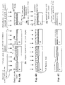
- FIG. 1 is a schematic view describing an example of forming a resist pattern for manufacturing a T type gate electrode using the resist material of the present invention.
- FIG. 2 is a schematic view describing another example of forming a resist pattern for manufacturing a T type gate electrode using the resist material of the present invention.
- FIGS. 3A and 3B are upper surface views of a FLASH EPROM that is one example of a semiconductor device according to the present invention.
- FIG. 4A through 4C are schematic sectional views (1) for describing a manufacturing method for FLASH EPROM that is one example of a manufacturing method for semiconductor device according to the present invention.
- FIG. 5D through 5F are schematic sectional views (2) for describing a manufacturing method for FLASH EPROM that is one example of a manufacturing method for semiconductor device according to the present invention.
- FIG. 6G through 6I are schematic sectional views (3) for describing a manufacturing method for FLASH EPROM that is one example of a manufacturing method for semiconductor device according to the present invention.
- FIG. 7A through 7C are schematic sectional views for describing a manufacturing method for EPROM that is another embodiment of the manufacturing method for semiconductor device according to the present invention.
- FIG. 8A through 8C are schematic sectional views for describing a manufacturing method for EPROM that is another embodiment of the manufacturing method for semiconductor device according to the present invention.
- FIG. 9A through 9D are schematic sectional views for describing one example of the application of a resist pattern thickened by use of the resist pattern thickening material of the present invention to manufacture of a magnetic head.
- FIG. 10 is a schematic sectional view for describing a process (1) of another example of the application of the resist pattern thickened by use of the resist pattern thickening material of the present invention to manufacture of a magnetic head.
- FIG. 11 is a schematic sectional view for describing a process (2) of another example of the application of the resist pattern thickened by use of the resist pattern thickening material of the present invention to manufacture of a magnetic head.
- FIG. 12 is a schematic sectional view for describing a process (3) of another example of the application of the resist pattern thickened by use of the resist pattern thickening material of the present invention to manufacture of a magnetic head.
- FIG. 13 is a schematic sectional view for describing a process (4) of another example of the application of the resist pattern thickened by use of the resist pattern thickening material of the present invention to manufacture of a magnetic head.
- FIG. 14 is a schematic sectional view for describing a process (5) of another example of the application of the resist pattern thickened by use of the resist pattern thickening material of the present invention to manufacture of a magnetic head.
- FIG. 15 is a schematic sectional view for describing a process (6) of another example of the application of the resist pattern thickened by use of the resist pattern thickening material of the present invention to manufacture of a magnetic head.
- FIG. 16 is a plan view showing one example of the magnetic head manufactured in the processes of FIGS. 10-15 .
- the resist material of the present invention contains a first photo-acid generator and a second photo-acid generator. It also contains a resin (also referred to as a “base material resin”), a solvent, and other suitable components which may be selected as necessary.
- a resin also referred to as a “base material resin”
- solvent also referred to as a “base material resin”
- This first photo-acid generator is a compound which exhibits an absorption peak to exposure light having a wavelength of less than 300 nm, and which generates an acid when irradiated by this exposure light.
- the aforementioned first photo-acid generator there is no particular limitation on the aforementioned first photo-acid generator provided that it is the aforementioned compound. It may be selected according to the purpose, but it is preferred that the number of molecules which react to exposure light having a wavelength of 300 nm or more, is 1 ⁇ 5 of the number of molecules which react to exposure light having a wavelength of less than 300 nm. Also, it is more preferred that it is an onium salt compound. From a viewpoint of sensitivity and resolution of the aforementioned resist material, it is particularly preferred that it is an onium salt compound expressed by the general formula I: (R 1 ) + X ⁇ . One of these compounds may be used alone, or two or more may be used together.
- (R 1 ) + represents a cation having the following structural formula, and specifically represents triallyl sulphonium cation or diallyl iodinium cation. Of these, triphenylsulphonium cation and diphenyliodonium cation are particularly preferred.
- R 2 represents a substituent, for example a hydrogen atom, a halogen atom, a straight chain, branched or cyclic alkyl group, or a straight chain, branched or cyclic alkoxy group. These may be substituted by substituent groups. It is preferred that the number of carbon atoms in the alkyl group or alkoxy group is, for example, about one to six. There is no particular limitation on the substitution position of R 2 , which may be suitably selected according to the purpose.
- X ⁇ represents an anion, and specifically, C n F 2n+1 SO 3 — or the like is preferred.
- the exposure light having a wavelength of less than 300 nm there is no particular limitation on the exposure light having a wavelength of less than 300 nm and it may be suitably selected according to the purpose, but a charged particle beam or the like is more preferred.
- the amount of the first photo-acid generator in the resist material and the second photo-acid generator, resin, solvent and other components may be suitably selected as required.
- This second photo-acid generator is a compound which exhibits an absorption peak to exposure light having a wavelength of higher than 300 nm, and which generates an acid when irradiated by this exposure light.
- the aforementioned second photo-acid generator there is no particular limitation on the aforementioned second photo-acid generator provided that it is the aforementioned compound. It may be selected according to the purpose, but it is preferred that the number of molecules which react to exposure light having a wavelength of less than 300 nm, is 1 ⁇ 5 of the number of molecules which react to exposure light having a wavelength of 300 nm or more. It is preferred that it is at least one type of compounds expressed by the following general formulae (II)-(1)-(9). One of these compounds may be used alone, or two or more may be used together.
- the exposure light of wavelength 300 nm or more which may be suitably selected according to the purpose, from the viewpoint of performing efficient patterning, ultraviolet radiation is preferred, and the g line (wavelength 436 nm) or i line (wavelength 365 nm) of a mercury vapor lamp is more preferred.
- the amount of the resist material in the second photo-acid generator there is no particular limitation on the amount of the resist material in the second photo-acid generator, and it may be suitably selected according to the second photo-acid generator, resin, solvent and other components.
- the resin which may be suitably selected from resins known as base material resins in resist materials according to the art, but it preferably contains at least one species selected from (meth)acrylic ester polymer, vinyl phenol polymer, N-substituted maleimide polymer, styrene polymer, cycloolefin maleic acid anhydride (COMA) polymer, cycloolefin polymer, (meth)acrylic ester/cycloolefin maleic acid anhydride copolymer, fumaric acid polymer, vinyl benzoic acid polymer, norbornane carboxylic acid and itaconic acid polymer.
- COMPA cycloolefin maleic acid anhydride
- (Meth)acrylic ester polymer is more preferred in the deep ultraviolet range from the viewpoint that high transparency can be maintained.
- a polarity changeable resin using a catalytic proton reaction is preferred.
- One of these may be used alone, or two or more may be used together.
- the resist material is a chemically amplified type resist material.
- the aforementioned protective group which is acid dissociative in a positive resist dissociates and the alkali dissolution rate improves, whereas in a negative resist, due to the crosslinking reaction of the crosslinking agent, the alkali dissociation rate falls.
- the polarity changeable resin it is preferred from the viewpoint of balance between ease of patterning and solubility in a basic aqueous solution, that 5-80% of all polar groups in this resin are replaced by a protective group, and if the resin is a copolymer, that the crosslinking rate in this copolymer is 5-80%. Moreover, from the viewpoint of maintaining ease of patterning and solubility in a basic aqueous solution at a high level, that 20-80% of all polar groups in this resin are replaced by a protective group, and that the crosslinking rate in the copolymer is 20-80%.
- the protective group which may be suitably selected according to the purpose, but from the viewpoint of utilizing a change of polarity in hydrophilicity by elimination of the protective group, a hydrophobic protective group is preferred.
- hydrophobic protective group which may be suitably selected according to the purpose, but it is preferably at least one of t-butoxy carbonyl, tetrahydropyrane, t-butyl or an alicyclic functional group.
- the alicyclic functional group is at least one species selected from substituents expressed by the following structural formula A, and substituents expressed by the following structural formula B.
- a lactone functional group is preferred among the substituents expressed by the structural formula A.
- the 5-member lactone ring dissociates due to the action of the first photo-acid generator or second photo-acid generator represented by “PAG” when irradiated by light, the carboxyl group substituted by the 5-member lactone ring becomes a carboxyl group, H + (protons) are generated and the alkali dissolution rate improves, as shown by the following reaction equation.
- the substituent expressed by the following structural formula B has the following structural formula, and particularly preferred that it is an adamantyl functional group or a norbornane functional group.
- the aforementioned resin is a copolymer
- the monomer unit of this copolymer there is no particular limitation on the monomer unit of this copolymer, and it may be suitably selected according to the purpose. Examples are ⁇ -butyrolactone-3-ilmethacrylate or 2-alkyl-2-adamantyl methacrylate.
- a suitable example of the copolymer is the copolymer of ⁇ -butyrolactone-3-ilmethacrylate and 2-alkyl-2-adamantyl methacrylate shown below.
- n and m in the formula represent the degree of polymerization.
- the mass average molecular weight of the aforementioned resin which may be suitably selected according to the purpose, but it is preferably 2,000-1,000,000 and more preferably 3,000-50,000.
- solvents used in the art for resist materials there is no particular limitation on the aforementioned solvent which may be suitably selected from solvents used in the art for resist materials according to the purpose, convenient examples are ethyl lactate, methyl amyl ketone, methyl-3-methoxypropionate, ethyl amyl ketone, methyl-3-methoxypropionate, ethyl-3-ethoxypropionate and propylene glycol methyl ether acetate. One of these may be used alone, or two or more may be used together.
- the amount of the aforementioned resist material in the solvent which may be suitably selected according to fitness for application such as coating homogeneity at the time of application, and thickness of the resist formed.
- an auxiliary solvent may be added to the aforementioned solvent (main solvent).
- butyl acetate, ⁇ -butyrolactone and propylene glycol methyl ether may for example be mentioned.
- One of these may be used alone, or two or more may be used together.
- the amount of auxiliary solvent used is preferably 1-30 mass %, and more preferably 10-20 mass %, relative to the main solvent.
- the crosslinking agent when the aforementioned resist material is a negative type may be various well-known additives, for example, N-methylpyrrolidone (basic additive).
- the type and amount of other components in the aforementioned resist material differ according to the first photo-acid generator, second photo-acid generator, resin and organic solvent, and cannot be uniquely specified, but they may be suitably selected according to the purpose.
- the aforementioned crosslinking agent is used when the aforementioned resist material is a negative type.
- it may be suitably selected according to the purpose, but an alkali soluble agent which produces crosslinking due to acids is preferred, for example, an amino crosslinking agent.
- the amino crosslinking agent may for example conveniently be a melamine derivative, urea derivative or uril derivative. One of these may be used alone, or two or more may be used together.
- the urea derivative may for example be urea, alkoxy methylene urea, N-alkoxy methylene urea, ethylene urea, ethylene urea carboxylic acid or their derivatives.
- the melamine derivative may for example be methylene or alkoxymethylene melamine, or its derivatives.
- the uril derivative may for example be benzoguanamine or glycouril, or their derivatives.
- the amount of crosslinking agent in the resist material is different according to the type and content of the resin or water-soluble aromatic compound and cannot be specified uniquely, it may be determined suitably according to the purpose.
- the absorbance in the wavelength region of this ultraviolet radiation is 1.75 or less, and more preferred that the absorbance in the far ultraviolet range is 1.6 or less.
- the resist material of the present invention in the case of a positive resist, may be obtained by forming a resist film by coating on a substrate, exposing it in a fine pattern using exposure light (e.g., a charged particle beam) having a wavelength of less than 300 nm, and exposing a relatively large pattern using exposure light (e.g., ultraviolet light) having a wavelength of 300 nm or more, or the exposure is performed in the reverse sequence. After each individual exposure or after all the exposures, the product is baked and developed to form a fine pattern by the resist pattern. On the other hand, in the case of a negative resist, baking and developing are performed after all exposures so as to form a fine pattern by the resist pattern.
- exposure light e.g., a charged particle beam
- exposure light e.g., ultraviolet light
- the method for forming the resist pattern by the resist material of the present invention and the size and thickness of the resist pattern are not particularly limited, and may be suitably selected according to the purpose.
- the thickness may be suitably determined by the underlying layer (substrate) which is being patterned and by etching conditions, but it is generally of the order of 0.1-10 ⁇ m and preferred that it is of the order of 0.2-2 ⁇ m.
- the resist material of the present invention may be conveniently used to form patterns in which the opening diameter (an opening diameter in a case of hole pattern, and a distance between adjacent patterns, in a case of line pattern) is less than 10 ⁇ m, and in particular to form patterns in which the opening diameter (an opening diameter in a case of hole pattern, and a distance between adjacent patterns, in a case of line pattern) is less than 0.2 ⁇ m when the exposure light is a charged particle beam or to manufacture high electron transfer transistor devices.
- the following may be used for the resist pattern, the method for manufacturing the resist pattern, the semiconductor devices and the method for manufacturing semiconductor devices according to the present invention.
- the resist pattern of the present invention may conveniently be formed by the method for manufacturing resist patterns of the present invention, described hereafter.
- the resist pattern of the present invention may for example conveniently be used for functional parts such as mask patterns, reticle patterns, magnetic heads, LCD (Liquid Crystal Displays), PDP (Plasma Display Panels) or SAW filters (Surface Acoustic Wave Filters), optical parts used for wiring by light, minute devices such as micro-actuators and semiconductor devices, and may also be conveniently used for the semiconductor device of the present invention, described later.
- functional parts such as mask patterns, reticle patterns, magnetic heads, LCD (Liquid Crystal Displays), PDP (Plasma Display Panels) or SAW filters (Surface Acoustic Wave Filters), optical parts used for wiring by light, minute devices such as micro-actuators and semiconductor devices, and may also be conveniently used for the semiconductor device of the present invention, described later.
- the method for manufacturing the resist pattern of the present invention comprises a step for forming resist film, A) a step for selectively exposing and B) a step for selectively exposing, and may also comprise a step for baking, a step for developing and another step if required.
- the step for forming resist film is a step which forms a resist film using the resist material of the present invention.
- the method for forming the resist film which may be conveniently selected from among those known in the art, but for example it is convenient to form the resist film by coating the resist material.
- the resist film may be formed on an underlying layer (substrate).
- an underlying layer substrate
- the underlying layer substrate
- the underlying layer is a substrate such as a silicon wafer or the like.
- the step for selectively exposing is a step which selectively exposes the resist film formed in the step for forming resist film using exposure light having a wavelength of less than 300 nm.
- the exposure light having a wavelength of less than 300 nm there is no particular limitation on the exposure light having a wavelength of less than 300 nm and this may be conveniently selected according to the purpose, but a charged particle beam is particularly preferred.
- An exposure device may be used for the exposure, such as for example an EB exposure device.
- the step for selectively exposing is a step which selectively exposes the resist film formed in the step for forming resist film using exposure light having a wavelength of 300 nm or more.
- the exposure light having a wavelength of 300 nm or more there is no particular limitation on the exposure light having a wavelength of 300 nm or more, and this may be conveniently selected according to the purpose, but from the viewpoint of efficient patterning, ultraviolet light is preferred and the g line (wavelength 436 nm) or i line (wavelength 365 nm) is particularly preferred.
- An exposure device may be used for the exposure, such as for example a mercury vapor lamp.
- the A) step for selectively exposing or B) step for selectively exposing may be performed first.
- Baking is a step which bakes the resist film which has been exposed after the step for selectively exposing and step for selectively exposing.
- the conditions and method for baking there is no particular limitation on the conditions and method for baking, and these may be conveniently selected according to the purpose, however the temperature is for example of the order of 70-150° C. but preferably 90-130° C., and the time is of the order of 10 secs-5 minutes but preferably 40 secs-100 secs.
- Developing is a step which develops the resist film after exposure.
- developing in water or developing in a weakly alkaline aqueous solution may be performed, but from the viewpoint of low cost and efficiency, developing in water is preferred.
- a resist film is formed by coating on a substrate, exposing it in a step for selectively exposing which exposes fine patterns using exposure light (e.g., a charged particle beam) having a wavelength of less than 300 nm, and exposing it in a step for selectively exposing which exposes relatively large patterns using exposure light (e.g., ultraviolet light) having a wavelength of 300 nm or more, or conversely, the step for selectively exposing is performed after the step for selectively exposing.
- exposure light e.g., a charged particle beam
- exposure light e.g., ultraviolet light
- the step for baking and step for developing are performed after the step for selectively exposing or step for selectively exposing, or after the step for selectively exposing and step for selectively exposing, so as to form the fine patterns by the resist pattern.
- the step for baking and step for developing are performed after the step for selectively exposing and step for selectively exposing so as to form fine patterns from the resist pattern.
- the resist pattern formed by the method for forming a resist pattern of the present invention is the resist pattern of the present invention.
- This resist pattern may for example conveniently be used for functional parts such as mask patterns, reticle patterns, magnetic heads, LCD (Liquid Crystal Displays), PDP (Plasma Display Panels) or SAW filters (Surface Acoustic Wave Filters), optical parts used for wiring by light, minute devices such as micro-actuators and semiconductor devices, and may also be conveniently used for the semiconductor device of the present invention, described later.
- the method for manufacturing the resist pattern of the present invention may conveniently be used for forming a pattern having an opening diameter (an opening diameter in a case of hole pattern, and a distance between adjacent patterns, in a case of line pattern) of 0.2 ⁇ m or less, may conveniently be used for manufacturing a high electron mobility transistor device, and may, in particular, conveniently be used for the semiconductor device and method for manufacturing a semiconductor device for the present invention.
- the semiconductor device of the present invention comprises a pattern from the resist pattern of the present invention, and it comprises parts known in the art which may be suitably selected according to the purpose.
- semiconductor device of the present invention are flash memories, DRAM, FRAM and high electron mobility transistor devices.
- the semiconductor device of the present invention may be conveniently manufactured by the method for manufacturing a semiconductor device for the present invention described below.
- the method for manufacturing a semiconductor device for the present invention comprises a step for forming resist pattern and a step for patterning, and may also comprise other steps which are suitably selected according to the need.
- the step for forming resist pattern is a step which forms a resist pattern on the underlying layer by the aforementioned method for forming a resist pattern.
- the underlying layer on which the resist pattern is formed may be a surface layer of various parts of the semiconductor device, the substrate of a silicon wafer or its surface layer.
- the resist film formed by the resist material comprises at least two layers.
- a large opening may be formed in the upper layer, and a smaller opening than this opening may be formed in the lower layer.
- a large opening may be formed in the middle layer, and a smaller opening than this opening may be formed in the lower layer.
- the resist material of the present invention may be used for the resist film.
- a chemically amplified material when the resist film has a two-layer construction, a chemically amplified material may conveniently be used in the upper layer, and when the resist film has a three-layer construction, a chemically amplified material may conveniently be used in the middle layer, i.e., in the layer above the lower layer.
- the upper layer when the upper layer is patterned, the upper layer may be formed into a reverse taper shape after developing by suitably selecting exposure conditions, as shown in FIGS. 1 and 2 .
- the step for patterning is a step for patterning wherein etching is performed using the resist pattern formed by the step for forming resist pattern as a mask.
- etching method which may be suitably selected according to the purpose from the methods known in the art, e.g., dry etching.
- etching conditions which may be suitably selected according to the purpose.
- various types of semiconductor device may be efficiently manufactured including for example, flash memories, DRAM, FRAM and high electron mobility transistor devices.
- a positive type resist material comprising 100 mass parts of polyvinyl phenol (wherein 30 percent of total polarity is substituted by t-butoxycarbonyl groups) as the resin, 2 mass parts of diphenyliodonium triphlate as the first photo-acid generator, 5 mass parts of a substance wherein, in the general formula (II)-(1), R ⁇ CH 3 as the second photo-acid generator, and 400 mass parts of propylene glycol monomethylether acetate as the solvent.
- a resist pattern was formed using this positive resist material.
- the positive resist material was coated on a Si substrate by spin coating, and a resist film was formed by baking at 100° C. for 60 seconds.
- This resist film was exposed to the i line (365 nm) to form a rectangle of 1 ⁇ m side using an exposure device.
- a post-exposure bake (PEB) was performed at 100° C. for 60 seconds, and it was then exposed to a charged particle beam to give an isolated line pattern of 0.10 ⁇ m width at a different position from the exposure position of the i line using an EB exposure device. After exposure, it was baked at 100° C. for 60 seconds. Subsequently, it was developed for 60 seconds using a 2.38 mass % aqueous solution of tetramethylammonium hydroxide.
- a resist pattern was formed using this positive resist material by the following processes A and B.
- the positive resist material prepared in Example 1 was coated on a Si substrate by spin coating, and a resist film was formed by baking at 120° C. for 60 seconds.
- this resist film was exposed to the g line (436 nm) to form a rectangle of 20 ⁇ m side using an exposure device.
- a post-exposure bake (PEB) was performed at 120° C. for 60 seconds.
- the product was developed for 60 seconds using a 2.38 mass % aqueous solution of tetramethylammonium hydroxide.
- it was exposed to a charged particle beam to give an isolated line pattern of 0.05 ⁇ m width at a different position from the exposure position of the g line using an EB exposure device. After exposure, it was baked at 120° C. for 60 seconds. Subsequently, it was developed for 60 seconds using a 2.38 mass % aqueous solution of tetramethylammonium hydroxide.
- the positive resist material prepared in Example 1 was coated on a Si substrate by spin coating, and a resist film was formed by baking at 120° C. for 60 seconds.
- this resist film was exposed to the g line (436 nm) to form a rectangle of 20 ⁇ m side using an exposure device.
- it was exposed to a charged particle beam to give an isolated line pattern of 0.05 ⁇ m width at a different position from the exposure position of the g line using an EB exposure device. After exposure, it was baked at 120° C. for 60 seconds. Subsequently, it was developed for 60 seconds using a 2.38 mass % aqueous solution of tetramethylammonium hydroxide.
- a resist pattern was formed using this negative resist material.
- the negative resist material was coated on a Si substrate by spin coating, and a resist film was formed by baking at 100° C. for 60 seconds.
- This resist film was exposed to the i line (365 nm) to form a rectangle of 10 ⁇ m side using an exposure device.
- a post-exposure bake (PEB) was performed at 100° C. for 60 seconds.
- PEB post-exposure bake
- a positive resist material was prepared as in Example 1 except that, in Example 1, the second photo-acid generator was a substance expressed by the general formula (II)-(4) wherein R ⁇ H, and a resist pattern was formed using this positive resist material.
- a positive resist material was prepared as in Example 1 except that, in Example 1, the second photo-acid generator was a substance expressed by the general formula (II)-(5), and a resist pattern was formed using this positive resist material.
- a positive resist material was prepared as in Example 1 except that, in Example 1, the second photo-acid generator was a substance expressed by the general formula (II)-(6) wherein R 1 , R 2 ⁇ H, and a resist pattern was formed using this positive resist material.
- a positive resist material was prepared as in Example 1 except that, in Example 1, the second photo-acid generator was a substance expressed by the general formula (II)-(9), and a resist pattern was formed using this positive resist material.
- Example 10 is an example of the semiconductor device of the present invention using the resist material of the present invention, and its method for manufacture.
- the resist films 26 , 27 , 29 , 32 and 34 described below are formed by an identical method to that of Example 1 using the resist material of the present invention.
- FIGS. 3A and 3B are upper surface views (plan views) of a FLASH EPROM called FLOTOX type or ETOX type.
- FIGS. 4A-C , FIGS. 5D-F , and FIGS. 6G-I are schematic sectional views for illustrating one example for the manufacturing method for the FLASH EPROM, wherein the left views in FIGS. 4A-6I are schematic sectional (A-directional sectional) views in the gate lateral direction (X-direction in FIG. 3A ) of the part for forming a MOS transistor having a floating gate electrode in a memory cell part (first element region), the central views are schematic sectional (B-directional sectional) views in the gate longitudinal direction (Y-direction in FIG.
- FIG. 3A orthogonal to the X-direction in the memory cell part of the same part as in the left views, and the right views are schematic sectional (A-directional sectional in FIG. 3B ) views of the part for forming a MOS transistor in a peripheral circuit part (second element region).
- a field oxide film 23 by SiO 2 film was selectively formed on the element separating region on a p-type Si substrate 22 as shown in FIG. 4A . Thereafter, a first gate insulation film 24 a in the MOS transistor of the memory cell part (first element region) was formed with SiO 2 film by thermal oxidation so as to have a thickness of 100-300 ⁇ , and a second gate insulation film 24 b in the MOS transistor of the peripheral circuit part (second element region) was also formed with SiO 2 film by thermal oxidation so as to have a thickness of 100-500 ⁇ in another process. When the first gate insulation film 24 a and the second gate insulation film 24 b are formed in the same thickness, the oxide films may be formed simultaneously in the same process.
- the peripheral circuit part (the right view in FIG. 4A ) was masked with a resist film 26 for the purpose of controlling threshold voltage.
- a resist film 26 for the purpose of controlling threshold voltage.
- phosphor (P) or arsenic (As) was introduced as n-type impurity in a dose of 1 ⁇ 10 11 -1 ⁇ 10 14 cm ⁇ 2 by ion implantation to form a first threshold control layer 25 a .
- the dose and conductive type of the impurity can be properly selected depending on selection of depression type or accumulation type.
- the memory cell part (the left and central views in FIG. 4B ) was masked with a resist film 27 for the purpose of controlling the threshold voltage.
- a resist film 27 for the purpose of controlling the threshold voltage.
- phosphor (P) or arsenic (As) was introduced as n-type impurity in a dose of 1 ⁇ 10 11 -1 ⁇ 10 14 cm ⁇ 2 by ion implantation to form a second threshold control layer 25 b.
- a first polysilicon film (first conductor film) 28 500-2000 ⁇ thick was formed on the whole surface as the floating gate electrode of the MOS transistor of the memory cell part (the left and central views in FIG. 4C ) and the gate electrode of the MOS transistor of the peripheral circuit part (the right view in FIG. 4C ).
- the first polysilicon film 28 was patterned with a resist film 29 formed as a mask, as shown in FIG. 5D , to form a floating gate electrode 28 a in the MOS transistor of the memory cell part (the left and central views in FIG. 5D ). At this time, the patterning was performed in X-direction so as to have a final dimension width, as shown in FIG. 5D , but not in Y-direction to leave the region for forming a S/D region layer as covered with the resist film 29 .
- a capacitor insulation film 30 a consisting of SiO 2 film was formed in a thickness of about 200-500 ⁇ by thermal oxidation so as to cover the floating gate electrode 28 a .
- a capacitor insulating film 30 b consisting of SiO 2 film is also formed on the first polysilicon film 28 of the peripheral circuit part (the right view in FIG. 5E ).
- the capacitor insulation films 30 a and 30 b which were formed of only SiO 2 films herein, may be formed of a composite film consisting of SiO 2 film and Si 3 N 4 film laminated in 2-3 layers.
- a second polysilicon film (second conductor film) 31 forming a control gate electrode was formed in a thickness of 500-2000 ⁇ , as shown in FIG. 5E , so as to cover the floating gate electrode 28 a and the capacitor insulation film 30 a.
- the memory cell part (the left and central views in FIG. 5F ) was masked with a resist film 32 as shown in FIG. 5F , and the second polysilicon film 31 and capacitor insulation film 30 b of the peripheral circuit part (the right view in FIG. 5F ) were successively removed by etching to expose the first polysilicon film 28 .
- the second polysilicon film 31 , capacitor insulation film 30 a and first polysilicon film 28 a patterned only in X-direction of the memory cell part were patterned in Y-direction with the resist film 32 as a mask so as to have the final dimension of a first gate part 33 a as shown in FIG. 6G , whereby a lamination by a control gate electrode 31 a/a capacitor insulation film 30 c /a floating gate electrode 28 c about 1 ⁇ m in width was formed in Y-direction.
- the first polysilicon film 28 of the peripheral circuit part (the right view in FIG. 6G ) was also patterned with the resist film 32 as a mask so as to have the final dimension of a second gate part 33 b , whereby a gate electrode 28 b about 1 ⁇ m in width was formed.
- phosphor (P) or arsenic (As) was introduced as n-type impurity in a dose of 1 ⁇ 10 14 -1 ⁇ 10 16 cm ⁇ 2 to the Si substrate 22 in the element forming region to form S/D region layers 36 a and 36 b.
- An interlayer insulation film 37 by PSG film was formed in a thickness of about 5000 ⁇ so as to cover the first gate part 33 a of the memory cell part (the left and central views in FIG. 6I ) and the second gate part 33 b of the peripheral circuit part (the right view in FIG. 6I ).
- contact holes 38 a and 38 b and contact holes 39 a and 39 b were formed in the interlayer insulating film 37 formed on the S/D region layers 35 a and 35 b and the S/D region layers 36 a and 36 b , and S/D electrodes 40 a and 40 b and S/D electrodes 41 a and 41 b were then formed.
- a FLASH EPROM was manufactured as semiconductor device as shown in FIG. 6I .
- the second gate insulating film 24 b of the peripheral circuit part (the right views in FIGS. 4A-5F ) are always covered with the first polysilicon film 28 or gate electrode 28 b after the formation (the right views in FIGS. 5C-5F ), the second gate insulating film 24 b keeps the originally formed thickness. Therefore, the thickness control of the second gate insulating film 24 b can be facilitated, and the adjustment of conductive impurity concentration for the control of threshold voltage can be also facilitated.
- the patterning for the formation of the first gate part 33 a is performed with a prescribed width first in the gate lateral direction (X-direction in FIG. 3A ) and then in the gate longitudinal direction (Y-direction in FIG. 3A ) to form a final prescribed width, but the patterning may be reversely performed with the prescribed width first in the gate longitudinal direction (Y-direction in FIG. 3A ) and then in the gate lateral direction (X-direction in FIG. 3A ) to form the final prescribed width.
- the example of manufacture of FLASH EPROM shown in FIGS. 7A-C is the same as the above example except changing the following process after the process shown in FIG. 5F in the above embodiment as shown in FIGS. 7A-C .
- the different point from the above example is that a high melting point metallic membrane (fourth conductor film) 42 consisting of tungsten (W) film or titanium (Ti) film was formed in a thickness of about 2000 ⁇ on the second polysilicon film 31 of the memory cell part (the left and central views in FIG. 7A ) and the first polysilicon film 28 of the peripheral circuit part (the right view in FIG. 7A ) to provide a polycide film.
- FIGS. 7B-C were performed in the same manner as in FIGS. 6G-I .
- the description for the same process as FIGS. 6G-I was omitted, and the same part as in FIGS. 6G-I was shown by the same reference mark in FIGS. 7A-C .
- a FLASH EPROM was manufactured as semiconductor device as shown in FIG. 7C .
- a high melting point metal silicide membrane such as titanium silicide (TiSi) membrane, etc. may be used in addition to the above-mentioned high melting point metallic membranes (fourth conductor films) 42 a and 42 b.
- the example of manufacture of FLASH EPROM shown in FIGS. 8A-C is the same as the above example except constituting the second gate part 33 c of the peripheral circuit part (second element region) (the right view in FIG. 8A ) to have a structure consisting of a first polysilicon film 28 b (first conductor film)/a SiO 2 film 30 d (capacitor insulation film)/a second polysilicon film 31 b (second conductor film) similarly to the first gate part 33 a of the memory cell part (first element region) (the left and central views in FIG. 8A ), and short-circuiting the first polysilicon film 28 b and the second polysilicon film 31 b to form a gate electrode as shown in FIG. 8B or C.
- an opening part 52 a extending through the first polysilicon film 28 b (first conductor film)/the SiO 2 film 30 d (capacitor insulation film)/the second polysilicon film 31 b (the second conductor film) is formed, for example, in a position different from the second gate part 33 c shown in FIG. 8A , e.g., on an insulation film 54 , and a third conductor film, for example, a high melting point metallic membrane 53 a such as W film, Ti film, etc. is buried in the opening part 52 a , whereby the first polysilicon film 28 b and the second polysilicon film 31 b are short-circuited.
- a third conductor film for example, a high melting point metallic membrane 53 a such as W film, Ti film, etc.
- an opening part 52 b extending through the first polysilicon film 28 b (first conductor film)/the SiO 2 film 30 d (capacitor insulation film) is formed to expose the first polysilicon film 28 b of the lower layer to the bottom of the opening part 52 b , and a third conductor film, for example, a high melting point metallic membrane 53 b such as W film, Ti film, etc. is buried in the opening part 52 b , whereby the first polysilicon film 28 b and the second polysilicon film 31 b are short-circuited.
- a third conductor film for example, a high melting point metallic membrane 53 b such as W film, Ti film, etc.
- the peripheral circuit part can be formed simultaneously with the formation of the memory cell part to effectively simplify the manufacturing process.
- the third conductor film 53 a or 53 b and the high melting point metallic membrane (fourth conductor film) 42 may be simultaneously formed as a common high melting point metallic membrane in addition to the above independent formation.
- Example 11 relates to the manufacture of a magnetic head, which is an example of the application of the resist pattern of the present invention using the resist material of the present invention.
- the resist patterns 102 and 126 described below are formed by an identical method to that of Example 1 using the resist material of the present invention.
- FIGS. 9A-D are flowcharts for illustrating the manufacture of the magnetic head.
- a resist film was formed on an interlayer insulation layer 100 in a thickness of 6 ⁇ m, as shown in FIG. 9A , followed by exposure and development to form a resist pattern 102 having an opening pattern for forming a spiroid thin film magnetic coil.
- a plating underlying layer 106 consisting of the lamination of a Ti adhesion layer 0.01 ⁇ m thick and a Cu adhesion layer 0.05 ⁇ m thick was formed by evaporation, as shown in FIG. 9B , on the resist pattern 102 and the part having no resist pattern 102 formed thereon or the exposed surface of the opening part 104 on the interlayer insulation layer 100 .
- a thin film conductor 108 consisting of a Cu plating film 3 ⁇ m thick was formed, as shown in FIG. 9C , in the part having no resist pattern 102 formed thereon, or on the surface of the plating underlying layer 106 formed on the exposed surface of the opening part 104 on the interlayer insulation layer 100 .
- the magnetic head was manufactured.
- the magnetic head obtained herein is finely formed as a spiroid pattern from the resist pattern 102 using the resist material of the present invention, so the thin film magnetic coil 110 is detailed and highly precise, and it is also excellent for mass production.
- FIGS. 10-15 are flowcharts for illustrating the manufacture of another magnetic head.
- a gap layer 114 was formed on a ceramic nonmagnetic substrate 112 by sputtering as shown in FIG. 10 .
- a resin insulation film 116 was formed by use of a thermosetting resin in a prescribed region on the gap layer 114 except the part forming the magnetic tip of the lower magnetic layer not shown. A resist material was then applied to the resin insulation film 116 to form a resist film 118 .
- the resist film 118 was then subjected to exposure and development, as shown in FIG. 11 , to form a spiroid pattern.
- the resist film 118 of the spiroid pattern was thermally set at several hundreds ° C. for about 1 hr as shown in FIG. 12 to form a projection-like first spiroid pattern 120 .
- a conductive underlying layer 122 consisting of Cu was further formed on the surface thereof so as to cover it.
- a resist material was applied onto the conductive underlying layer 122 by spin coating to form a resist film 124 , as shown in FIG. 13 , and the resist film 124 was patterned on the first spiroid pattern 120 to form a resist pattern 126 .
- a Cu conductor layer 128 is formed by plating, as shown in FIG. 14 , on the exposed surface of the conductive underlying layer 122 , or on the part having no resist pattern 126 formed thereon. Thereafter, the resist pattern 126 was lifted off, as shown in FIG. 15 , from the conductive underlying layer 122 by being dissolved and removed to form a spiroid thin film magnetic coil 130 by the Cu conductor layer 128 .
- the thin film magnetic coil 130 is minute and fine, and also excellent in mass-productivity.
- Example 12 is related to the manufacture of a T gate electrode, which is in example of the application of the resist pattern of the present invention using the resist material of the present invention.
- the lower layer 5 and upper layer 9 described below are formed from a chemically amplified type resist material.
- the lower layer 5 comprises a photo-acid generator which is photosensitive to a charged particle beam
- the upper layer 9 comprises a photo-acid generator which is sensitive to light (i line, g line, KrF laser, ArF laser).
- the resist material of the present invention was coated on a substrate 1 , the aforementioned step for selectively exposing was performed to form a reverse taper shaped pattern having a large opening, the step for selectively exposing was performed in this opening to form a smaller opening than this opening, a step for baking was performed wherein the product was baked at 70° C. for 120 seconds, developing was performed using a 2.38 mass % aqueous solution of tetramethylammonium hydroxide, and a resist pattern was formed to manufacture a T-gate electrode for high electron mobility transistor devices.
- the T gate electrode was formed by implanting a conductor by vacuum deposition inside the pattern (opening 3 ) due to this resist pattern.
- the above problems inherent in the prior art can be resolved in response to the demand, and a resist pattern which forms fine patterns suitable for semiconductor device manufacture, a method for forming a resist pattern which can manufacture these resist patterns efficiently in a short time, a resist material which is suitable for use in this resist pattern manufacture and can form fine patterns efficiently in a short time, a semiconductor device having these fine patterns formed by the resist pattern and a semiconductor manufacturing method which can manufacture this semiconductor device efficiently in a short time, are provided.
Priority Applications (2)
| Application Number | Priority Date | Filing Date | Title |
|---|---|---|---|
| US12/292,170 US7723016B2 (en) | 2001-11-27 | 2008-11-13 | Method for forming resist pattern and method for manufacturing a semiconductor device |
| US12/756,914 US8057986B2 (en) | 2001-11-27 | 2010-04-08 | Method for forming resist pattern and method for manufacturing a semiconductor device |
Applications Claiming Priority (4)
| Application Number | Priority Date | Filing Date | Title |
|---|---|---|---|
| JP2001361506A JP3901997B2 (ja) | 2001-11-27 | 2001-11-27 | レジスト材料、レジストパターン及びその製造方法、並びに、半導体装置及びその製造方法 |
| JP2001-361506 | 2001-11-27 | ||
| US10/107,203 US7465527B2 (en) | 2001-11-27 | 2002-03-28 | Resist material, resist pattern and forming method for the same, and a semiconductor device and manufacturing method for the same |
| US12/292,170 US7723016B2 (en) | 2001-11-27 | 2008-11-13 | Method for forming resist pattern and method for manufacturing a semiconductor device |
Related Parent Applications (1)
| Application Number | Title | Priority Date | Filing Date |
|---|---|---|---|
| US10/107,203 Division US7465527B2 (en) | 2001-11-27 | 2002-03-28 | Resist material, resist pattern and forming method for the same, and a semiconductor device and manufacturing method for the same |
Related Child Applications (1)
| Application Number | Title | Priority Date | Filing Date |
|---|---|---|---|
| US12/756,914 Division US8057986B2 (en) | 2001-11-27 | 2010-04-08 | Method for forming resist pattern and method for manufacturing a semiconductor device |
Publications (2)
| Publication Number | Publication Date |
|---|---|
| US20090081593A1 US20090081593A1 (en) | 2009-03-26 |
| US7723016B2 true US7723016B2 (en) | 2010-05-25 |
Family
ID=19172154
Family Applications (3)
| Application Number | Title | Priority Date | Filing Date |
|---|---|---|---|
| US10/107,203 Expired - Lifetime US7465527B2 (en) | 2001-11-27 | 2002-03-28 | Resist material, resist pattern and forming method for the same, and a semiconductor device and manufacturing method for the same |
| US12/292,170 Expired - Lifetime US7723016B2 (en) | 2001-11-27 | 2008-11-13 | Method for forming resist pattern and method for manufacturing a semiconductor device |
| US12/756,914 Expired - Fee Related US8057986B2 (en) | 2001-11-27 | 2010-04-08 | Method for forming resist pattern and method for manufacturing a semiconductor device |
Family Applications Before (1)
| Application Number | Title | Priority Date | Filing Date |
|---|---|---|---|
| US10/107,203 Expired - Lifetime US7465527B2 (en) | 2001-11-27 | 2002-03-28 | Resist material, resist pattern and forming method for the same, and a semiconductor device and manufacturing method for the same |
Family Applications After (1)
| Application Number | Title | Priority Date | Filing Date |
|---|---|---|---|
| US12/756,914 Expired - Fee Related US8057986B2 (en) | 2001-11-27 | 2010-04-08 | Method for forming resist pattern and method for manufacturing a semiconductor device |
Country Status (6)
Families Citing this family (27)
| Publication number | Priority date | Publication date | Assignee | Title |
|---|---|---|---|---|
| TW573227B (en) * | 2001-02-19 | 2004-01-21 | Sumitomo Chemical Co | Chemical amplifying type positive resist compositions |
| JP3901997B2 (ja) | 2001-11-27 | 2007-04-04 | 富士通株式会社 | レジスト材料、レジストパターン及びその製造方法、並びに、半導体装置及びその製造方法 |
| JP4410977B2 (ja) * | 2002-07-09 | 2010-02-10 | 富士通株式会社 | 化学増幅レジスト材料及びそれを用いたパターニング方法 |
| US7256873B2 (en) * | 2004-01-28 | 2007-08-14 | Asml Netherlands B.V. | Enhanced lithographic resolution through double exposure |
| JP4606136B2 (ja) | 2004-06-09 | 2011-01-05 | 富士通株式会社 | 多層体、レジストパターン形成方法、微細加工パターンを有する装置の製造方法および電子装置 |
| JP2006196034A (ja) * | 2005-01-11 | 2006-07-27 | Hitachi Global Storage Technologies Netherlands Bv | 磁気ヘッドの製造方法 |
| JP2006208546A (ja) * | 2005-01-26 | 2006-08-10 | Tokyo Ohka Kogyo Co Ltd | レジストパターン形成方法 |
| JP4801550B2 (ja) | 2006-09-26 | 2011-10-26 | 富士通株式会社 | レジスト組成物、レジストパターンの形成方法、及び半導体装置の製造方法 |
| KR100964787B1 (ko) * | 2007-04-16 | 2010-06-21 | 주식회사 엘지화학 | 광학필름 및 이를 포함하는 액정표시장치 |
| US7608865B1 (en) * | 2008-04-28 | 2009-10-27 | Northrop Grumman Space & Mission Systems Corp. | Club extension to a T-gate high electron mobility transistor |
| WO2011139073A2 (ko) * | 2010-05-04 | 2011-11-10 | 주식회사 엘지화학 | 네가티브 포토레지스트 조성물 및 소자의 패터닝 방법 |
| JP2012022227A (ja) * | 2010-07-16 | 2012-02-02 | San Apro Kk | フッ素化アルキルリン酸ヨードニウム系光酸発生剤含有エネルギー線硬化性組成物 |
| JP5659872B2 (ja) | 2010-10-22 | 2015-01-28 | 富士通株式会社 | レジストパターン改善化材料、レジストパターンの形成方法、及び半導体装置の製造方法 |
| JP5659873B2 (ja) | 2010-12-16 | 2015-01-28 | 富士通株式会社 | レジストパターン改善化材料、レジストパターンの形成方法、及び半導体装置の製造方法 |
| JP5708071B2 (ja) | 2011-03-11 | 2015-04-30 | 富士通株式会社 | レジストパターン改善化材料、レジストパターンの形成方法、及び半導体装置の製造方法 |
| JP5853844B2 (ja) * | 2011-05-20 | 2016-02-09 | 信越化学工業株式会社 | マイクロ構造体の製造方法及び光パターン形成性犠牲膜形成用組成物 |
| US9048184B2 (en) * | 2013-03-15 | 2015-06-02 | Northrop Grumman Systems Corporation | Method of forming a gate contact |
| JP2015015291A (ja) * | 2013-07-03 | 2015-01-22 | 東京エレクトロン株式会社 | 基板処理装置、基板処理システム、基板処理方法及び基板処理用記録媒体 |
| DE112015000546T5 (de) * | 2014-02-25 | 2016-11-10 | Tokyo Electron Limited | Chemische Verstärkungsverfahren und -methoden für entwickelbare untere Antireflexbeläge und gefärbte Implantationsresists |
| CN103885300B (zh) * | 2014-03-19 | 2016-01-27 | 南京晶奥微光电技术有限公司 | 一种疏水表面光刻工艺 |
| CN104465985A (zh) * | 2014-04-16 | 2015-03-25 | 贵州雅光电子科技股份有限公司 | 一种各向异性磁阻芯片的剥离法制备工艺 |
| JP6175455B2 (ja) * | 2015-01-22 | 2017-08-02 | 東京エレクトロン株式会社 | レジストパターン形成方法 |
| JP7185630B2 (ja) * | 2017-08-31 | 2022-12-07 | 富士フイルム株式会社 | 感活性光線性又は感放射線性樹脂組成物、レジスト膜、パターン形成方法、及び電子デバイスの製造方法 |
| TWI816764B (zh) | 2018-03-19 | 2023-10-01 | 日商東京威力科創股份有限公司 | 使用校準修整用劑之臨界尺寸校正方法 |
| US11269252B2 (en) * | 2019-07-22 | 2022-03-08 | Rohm And Haas Electronic Materials Llc | Method for forming pattern using antireflective coating composition including photoacid generator |
| US20210302839A1 (en) * | 2020-03-30 | 2021-09-30 | Taiwan Semiconductor Manufacturing Co., Ltd. | Method of manufacturing a semiconductor device |
| DE102020111895A1 (de) | 2020-04-30 | 2021-11-04 | Laser Imaging Systems Gmbh | Herstellung von dreidimensionalen Strukturen mittels Photoresisten |
Citations (28)
| Publication number | Priority date | Publication date | Assignee | Title |
|---|---|---|---|---|
| US4491628A (en) | 1982-08-23 | 1985-01-01 | International Business Machines Corporation | Positive- and negative-working resist compositions with acid generating photoinitiator and polymer with acid labile groups pendant from polymer backbone |
| JPH05197151A (ja) | 1992-01-21 | 1993-08-06 | Japan Synthetic Rubber Co Ltd | 感放射線性樹脂組成物 |
| EP0594452A2 (en) | 1992-10-22 | 1994-04-27 | Japan Synthetic Rubber Co., Ltd. | Radiation sensitive resin composition for microlens |
| US5403695A (en) | 1991-04-30 | 1995-04-04 | Kabushiki Kaisha Toshiba | Resist for forming patterns comprising an acid generating compound and a polymer having acid decomposable groups |
| JPH0798499A (ja) | 1993-09-28 | 1995-04-11 | Konica Corp | 感光性平版印刷版 |
| JPH07130651A (ja) | 1993-09-10 | 1995-05-19 | Toshiba Corp | 薄膜形成方法 |
| JPH07219216A (ja) | 1994-01-31 | 1995-08-18 | Nippon Kayaku Co Ltd | ポジ型感放射線性樹脂組成物及びそれを用いるパターン形成法 |
| JPH08262743A (ja) | 1995-03-24 | 1996-10-11 | Mitsubishi Electric Corp | レジスト材料およびレジストパターン形成方法 |
| JPH1073927A (ja) | 1996-07-05 | 1998-03-17 | Mitsubishi Electric Corp | 微細パターン形成材料及びこれを用いた半導体装置の製造方法並びに半導体装置 |
| JPH1097060A (ja) | 1996-09-20 | 1998-04-14 | Fuji Photo Film Co Ltd | ポジ型感光性組成物 |
| JPH11297597A (ja) | 1998-04-10 | 1999-10-29 | Toshiba Corp | パターン形成材料及びパターン形成方法 |
| US5994022A (en) * | 1996-11-14 | 1999-11-30 | Jsr Corporation | Radiation sensitive resin composition |
| US6027856A (en) | 1998-04-28 | 2000-02-22 | Fujitsu Limited | Negative-type resist composition and process for forming resist patterns |
| US6096478A (en) * | 1998-02-23 | 2000-08-01 | Nec Corporation | Resist material for forming a chemically amplified negative type resist pattern and method of manufacturing a semiconductor device employing the resist pattern |
| JP2000347414A (ja) | 1999-06-01 | 2000-12-15 | Tokyo Ohka Kogyo Co Ltd | レジストパターン微細化用塗膜形成剤及びそれを用いた微細パターン形成方法 |
| US6200728B1 (en) | 1999-02-20 | 2001-03-13 | Shipley Company, L.L.C. | Photoresist compositions comprising blends of photoacid generators |
| US6261743B1 (en) | 1997-02-07 | 2001-07-17 | Shipley Company, L.L.C. | Antireflective coating compositions comprising photoacid generators |
| JP2001228616A (ja) | 2000-02-16 | 2001-08-24 | Mitsubishi Electric Corp | 微細パターン形成材料及びこれを用いた半導体装置の製造方法 |
| US6280911B1 (en) | 1998-09-10 | 2001-08-28 | Shipley Company, L.L.C. | Photoresist compositions comprising blends of ionic and non-ionic photoacid generators |
| JP2002006491A (ja) | 2000-06-27 | 2002-01-09 | Fuji Photo Film Co Ltd | 電子線又はx線用ネガ型レジスト組成物 |
| JP2002049161A (ja) | 2000-08-04 | 2002-02-15 | Clariant (Japan) Kk | 被覆層現像用界面活性剤水溶液 |
| US6391520B1 (en) | 1998-05-25 | 2002-05-21 | Daicel Chemical Industries, Ltd. | Compounds for photoresist and resin composition for photoresist |
| US6440632B2 (en) * | 1997-12-19 | 2002-08-27 | Kansai Research Institute | Photosensitive resin composition and process for producing the same |
| US20030098464A1 (en) | 2001-11-27 | 2003-05-29 | Fujitsu Limited | Resist material, resist pattern and forming method for the same, and a semiconductor device and manufacturing method for the same |
| US6605417B2 (en) | 2000-02-04 | 2003-08-12 | Tokyo Ohka Kogyo Co., Ltd. | Method for decreasing surface defects of patterned resist layer |
| US6692888B1 (en) | 1999-10-07 | 2004-02-17 | Shipley Company, L.L.C. | Copolymers having nitrile and alicyclic leaving groups and photoresist compositions comprising same |
| US6749989B2 (en) | 2000-12-04 | 2004-06-15 | Tokyo Ohka Kogyo Co., Ltd. | Positive-working photoresist composition |
| US20050202352A1 (en) * | 2004-03-11 | 2005-09-15 | Worcester Polytechnic Institute | Systems and methods for sub-wavelength imaging |
Family Cites Families (1)
| Publication number | Priority date | Publication date | Assignee | Title |
|---|---|---|---|---|
| JP4533639B2 (ja) * | 2003-07-22 | 2010-09-01 | 富士フイルム株式会社 | 感刺激性組成物、化合物及び該感刺激性組成物を用いたパターン形成方法 |
-
2001
- 2001-11-27 JP JP2001361506A patent/JP3901997B2/ja not_active Expired - Lifetime
-
2002
- 2002-03-28 US US10/107,203 patent/US7465527B2/en not_active Expired - Lifetime
- 2002-03-28 DE DE60231077T patent/DE60231077D1/de not_active Expired - Lifetime
- 2002-03-28 EP EP02007431A patent/EP1315044B1/en not_active Expired - Lifetime
- 2002-03-29 TW TW091106378A patent/TWI305609B/zh not_active IP Right Cessation
- 2002-03-30 KR KR1020020017643A patent/KR100843909B1/ko active IP Right Grant
-
2008
- 2008-11-13 US US12/292,170 patent/US7723016B2/en not_active Expired - Lifetime
-
2010
- 2010-04-08 US US12/756,914 patent/US8057986B2/en not_active Expired - Fee Related
Patent Citations (31)
| Publication number | Priority date | Publication date | Assignee | Title |
|---|---|---|---|---|
| US4491628A (en) | 1982-08-23 | 1985-01-01 | International Business Machines Corporation | Positive- and negative-working resist compositions with acid generating photoinitiator and polymer with acid labile groups pendant from polymer backbone |
| US5403695A (en) | 1991-04-30 | 1995-04-04 | Kabushiki Kaisha Toshiba | Resist for forming patterns comprising an acid generating compound and a polymer having acid decomposable groups |
| JPH05197151A (ja) | 1992-01-21 | 1993-08-06 | Japan Synthetic Rubber Co Ltd | 感放射線性樹脂組成物 |
| EP0594452A2 (en) | 1992-10-22 | 1994-04-27 | Japan Synthetic Rubber Co., Ltd. | Radiation sensitive resin composition for microlens |
| JPH07130651A (ja) | 1993-09-10 | 1995-05-19 | Toshiba Corp | 薄膜形成方法 |
| JPH0798499A (ja) | 1993-09-28 | 1995-04-11 | Konica Corp | 感光性平版印刷版 |
| JPH07219216A (ja) | 1994-01-31 | 1995-08-18 | Nippon Kayaku Co Ltd | ポジ型感放射線性樹脂組成物及びそれを用いるパターン形成法 |
| US5679497A (en) | 1995-03-24 | 1997-10-21 | Mitsubishi Denki Kabushiki Kaisha | Resist material and method for forming resist pattern |
| JPH08262743A (ja) | 1995-03-24 | 1996-10-11 | Mitsubishi Electric Corp | レジスト材料およびレジストパターン形成方法 |
| JPH1073927A (ja) | 1996-07-05 | 1998-03-17 | Mitsubishi Electric Corp | 微細パターン形成材料及びこれを用いた半導体装置の製造方法並びに半導体装置 |
| JPH1097060A (ja) | 1996-09-20 | 1998-04-14 | Fuji Photo Film Co Ltd | ポジ型感光性組成物 |
| US5981140A (en) | 1996-09-20 | 1999-11-09 | Fuji Photo Film Co., Ltd. | Positive photosensitive composition |
| US5994022A (en) * | 1996-11-14 | 1999-11-30 | Jsr Corporation | Radiation sensitive resin composition |
| US6261743B1 (en) | 1997-02-07 | 2001-07-17 | Shipley Company, L.L.C. | Antireflective coating compositions comprising photoacid generators |
| US6440632B2 (en) * | 1997-12-19 | 2002-08-27 | Kansai Research Institute | Photosensitive resin composition and process for producing the same |
| US6096478A (en) * | 1998-02-23 | 2000-08-01 | Nec Corporation | Resist material for forming a chemically amplified negative type resist pattern and method of manufacturing a semiconductor device employing the resist pattern |
| JPH11297597A (ja) | 1998-04-10 | 1999-10-29 | Toshiba Corp | パターン形成材料及びパターン形成方法 |
| US6027856A (en) | 1998-04-28 | 2000-02-22 | Fujitsu Limited | Negative-type resist composition and process for forming resist patterns |
| US6391520B1 (en) | 1998-05-25 | 2002-05-21 | Daicel Chemical Industries, Ltd. | Compounds for photoresist and resin composition for photoresist |
| US6280911B1 (en) | 1998-09-10 | 2001-08-28 | Shipley Company, L.L.C. | Photoresist compositions comprising blends of ionic and non-ionic photoacid generators |
| US6200728B1 (en) | 1999-02-20 | 2001-03-13 | Shipley Company, L.L.C. | Photoresist compositions comprising blends of photoacid generators |
| JP2000347414A (ja) | 1999-06-01 | 2000-12-15 | Tokyo Ohka Kogyo Co Ltd | レジストパターン微細化用塗膜形成剤及びそれを用いた微細パターン形成方法 |
| US6692888B1 (en) | 1999-10-07 | 2004-02-17 | Shipley Company, L.L.C. | Copolymers having nitrile and alicyclic leaving groups and photoresist compositions comprising same |
| US6605417B2 (en) | 2000-02-04 | 2003-08-12 | Tokyo Ohka Kogyo Co., Ltd. | Method for decreasing surface defects of patterned resist layer |
| JP2001228616A (ja) | 2000-02-16 | 2001-08-24 | Mitsubishi Electric Corp | 微細パターン形成材料及びこれを用いた半導体装置の製造方法 |
| JP2002006491A (ja) | 2000-06-27 | 2002-01-09 | Fuji Photo Film Co Ltd | 電子線又はx線用ネガ型レジスト組成物 |
| JP2002049161A (ja) | 2000-08-04 | 2002-02-15 | Clariant (Japan) Kk | 被覆層現像用界面活性剤水溶液 |
| US6749989B2 (en) | 2000-12-04 | 2004-06-15 | Tokyo Ohka Kogyo Co., Ltd. | Positive-working photoresist composition |
| US20030098464A1 (en) | 2001-11-27 | 2003-05-29 | Fujitsu Limited | Resist material, resist pattern and forming method for the same, and a semiconductor device and manufacturing method for the same |
| JP3901997B2 (ja) | 2001-11-27 | 2007-04-04 | 富士通株式会社 | レジスト材料、レジストパターン及びその製造方法、並びに、半導体装置及びその製造方法 |
| US20050202352A1 (en) * | 2004-03-11 | 2005-09-15 | Worcester Polytechnic Institute | Systems and methods for sub-wavelength imaging |
Non-Patent Citations (2)
| Title |
|---|
| Japanese Office Action dated Sep. 12, 2006 of JP2001-361506. |
| Taiwanese Office Action dated Jun. 23, 2008 of TW 91106378. |
Also Published As
| Publication number | Publication date |
|---|---|
| US20100193841A1 (en) | 2010-08-05 |
| TWI305609B (en) | 2009-01-21 |
| US20090081593A1 (en) | 2009-03-26 |
| EP1315044B1 (en) | 2009-02-04 |
| KR20030043576A (ko) | 2003-06-02 |
| US8057986B2 (en) | 2011-11-15 |
| KR100843909B1 (ko) | 2008-07-03 |
| EP1315044A1 (en) | 2003-05-28 |
| JP2003162060A (ja) | 2003-06-06 |
| US7465527B2 (en) | 2008-12-16 |
| JP3901997B2 (ja) | 2007-04-04 |
| DE60231077D1 (de) | 2009-03-19 |
| US20030098464A1 (en) | 2003-05-29 |
Similar Documents
| Publication | Publication Date | Title |
|---|---|---|
| US7723016B2 (en) | Method for forming resist pattern and method for manufacturing a semiconductor device | |
| US7364829B2 (en) | Resist pattern thickening material, process for forming resist pattern, and process for manufacturing semiconductor device | |
| KR101439394B1 (ko) | 산 확산을 이용하는 더블 패터닝 공정에 의한 반도체소자의 미세 패턴 형성 방법 | |
| JP3690847B2 (ja) | レジスト組成物及びパターン形成方法 | |
| US6207342B1 (en) | Chemically amplified resist material and process for the formation of resist patterns | |
| US6800423B2 (en) | Radiation-sensitive composition and method for forming patterns and fabricating semiconductor devices | |
| KR19990081720A (ko) | 중합체 및 이를 이용한 미세패턴의 형성방법 | |
| KR101294510B1 (ko) | 레지스트 증감막 형성용 재료, 및 반도체 장치의 제조 방법 | |
| US20040029047A1 (en) | Micropattern forming material, micropattern forming method and method for manufacturing semiconductor device | |
| KR101690798B1 (ko) | 화학 증폭 포지티브형 레지스트 조성물 및 패턴 형성 방법 | |
| US8338072B2 (en) | Resist composition, resist pattern forming process, and method for manufacturing semiconductor device | |
| JP4686393B2 (ja) | レジスト組成物、レジストパターンの形成方法、半導体装置及びその製造方法 | |
| JP2004086203A (ja) | 微細パターン形成材料および電子デバイスの製造方法 | |
| US5994007A (en) | Pattern forming method utilizing first insulative and then conductive overlayer and underlayer | |
| US8029975B2 (en) | Fused aromatic structures and methods for photolithographic applications | |
| KR100732301B1 (ko) | 포토레지스트 중합체, 포토레지스트 조성물 및 이를 이용한반도체 소자의 제조 방법 | |
| JP5098592B2 (ja) | レジストパターン形状制御材料、半導体装置の製造方法、及び磁気ヘッドの製造方法 | |
| JP4127937B2 (ja) | レジスト組成物及びレジストパターンの形成方法 | |
| JP3619037B2 (ja) | パターン形成方法 | |
| JP3766235B2 (ja) | パタン形成方法および半導体装置の製造方法 | |
| JP2001174993A (ja) | 感放射線組成物およびパタン形成方法 | |
| JP2003098670A (ja) | レジスト組成物及びこれを用いたパターン形成方法 | |
| JP2002049149A (ja) | 電子線又はx線用ネガ型レジスト組成物 | |
| JPH04269756A (ja) | リフトオフ加工に適したレジスト膜 | |
| JP2002139834A (ja) | パタン形成方法および半導体装置の製造方法および感光性組成物 |
Legal Events
| Date | Code | Title | Description |
|---|---|---|---|
| STCF | Information on status: patent grant |
Free format text: PATENTED CASE |
|
| FEPP | Fee payment procedure |
Free format text: PAYOR NUMBER ASSIGNED (ORIGINAL EVENT CODE: ASPN); ENTITY STATUS OF PATENT OWNER: LARGE ENTITY |
|
| FPAY | Fee payment |
Year of fee payment: 4 |
|
| MAFP | Maintenance fee payment |
Free format text: PAYMENT OF MAINTENANCE FEE, 8TH YEAR, LARGE ENTITY (ORIGINAL EVENT CODE: M1552) Year of fee payment: 8 |
|
| MAFP | Maintenance fee payment |
Free format text: PAYMENT OF MAINTENANCE FEE, 12TH YEAR, LARGE ENTITY (ORIGINAL EVENT CODE: M1553); ENTITY STATUS OF PATENT OWNER: LARGE ENTITY Year of fee payment: 12 |