US7473929B2 - Semiconductor device and method for fabricating the same - Google Patents
Semiconductor device and method for fabricating the same Download PDFInfo
- Publication number
- US7473929B2 US7473929B2 US10/880,550 US88055004A US7473929B2 US 7473929 B2 US7473929 B2 US 7473929B2 US 88055004 A US88055004 A US 88055004A US 7473929 B2 US7473929 B2 US 7473929B2
- Authority
- US
- United States
- Prior art keywords
- layer
- channel layer
- region
- semiconductor device
- source region
- Prior art date
- Legal status (The legal status is an assumption and is not a legal conclusion. Google has not performed a legal analysis and makes no representation as to the accuracy of the status listed.)
- Active, expires
Links
- 239000004065 semiconductor Substances 0.000 title claims description 99
- 238000000034 method Methods 0.000 title description 46
- 239000002019 doping agent Substances 0.000 claims abstract description 110
- 239000000758 substrate Substances 0.000 claims abstract description 108
- 230000003746 surface roughness Effects 0.000 claims abstract description 67
- 229910052799 carbon Inorganic materials 0.000 claims abstract description 53
- OKTJSMMVPCPJKN-UHFFFAOYSA-N Carbon Chemical compound [C] OKTJSMMVPCPJKN-UHFFFAOYSA-N 0.000 claims abstract description 52
- 229910010271 silicon carbide Inorganic materials 0.000 claims description 162
- HBMJWWWQQXIZIP-UHFFFAOYSA-N silicon carbide Chemical compound [Si+]#[C-] HBMJWWWQQXIZIP-UHFFFAOYSA-N 0.000 claims description 161
- 238000001994 activation Methods 0.000 claims description 29
- 238000005498 polishing Methods 0.000 claims description 7
- 238000000137 annealing Methods 0.000 abstract description 49
- 238000005468 ion implantation Methods 0.000 abstract description 23
- 150000002500 ions Chemical class 0.000 abstract description 14
- 230000003213 activating effect Effects 0.000 abstract description 6
- 239000010410 layer Substances 0.000 description 370
- 238000002513 implantation Methods 0.000 description 36
- 239000007789 gas Substances 0.000 description 32
- 230000008569 process Effects 0.000 description 32
- VYPSYNLAJGMNEJ-UHFFFAOYSA-N Silicium dioxide Chemical compound O=[Si]=O VYPSYNLAJGMNEJ-UHFFFAOYSA-N 0.000 description 29
- 230000004913 activation Effects 0.000 description 27
- 229910052814 silicon oxide Inorganic materials 0.000 description 26
- PXHVJJICTQNCMI-UHFFFAOYSA-N nickel Substances [Ni] PXHVJJICTQNCMI-UHFFFAOYSA-N 0.000 description 21
- XKRFYHLGVUSROY-UHFFFAOYSA-N Argon Chemical compound [Ar] XKRFYHLGVUSROY-UHFFFAOYSA-N 0.000 description 16
- IJGRMHOSHXDMSA-UHFFFAOYSA-N Atomic nitrogen Chemical compound N#N IJGRMHOSHXDMSA-UHFFFAOYSA-N 0.000 description 15
- 229910052782 aluminium Inorganic materials 0.000 description 13
- XAGFODPZIPBFFR-UHFFFAOYSA-N aluminium Chemical compound [Al] XAGFODPZIPBFFR-UHFFFAOYSA-N 0.000 description 13
- 238000005530 etching Methods 0.000 description 13
- 238000004519 manufacturing process Methods 0.000 description 13
- KRHYYFGTRYWZRS-UHFFFAOYSA-N Fluorane Chemical compound F KRHYYFGTRYWZRS-UHFFFAOYSA-N 0.000 description 12
- ATUOYWHBWRKTHZ-UHFFFAOYSA-N Propane Chemical compound CCC ATUOYWHBWRKTHZ-UHFFFAOYSA-N 0.000 description 12
- BLRPTPMANUNPDV-UHFFFAOYSA-N Silane Chemical compound [SiH4] BLRPTPMANUNPDV-UHFFFAOYSA-N 0.000 description 12
- 239000000463 material Substances 0.000 description 12
- 230000015556 catabolic process Effects 0.000 description 9
- 238000001312 dry etching Methods 0.000 description 9
- 238000007254 oxidation reaction Methods 0.000 description 9
- 229910052786 argon Inorganic materials 0.000 description 8
- 239000001257 hydrogen Substances 0.000 description 8
- 229910052739 hydrogen Inorganic materials 0.000 description 8
- 238000000206 photolithography Methods 0.000 description 8
- 230000015572 biosynthetic process Effects 0.000 description 7
- 238000010438 heat treatment Methods 0.000 description 7
- 230000003647 oxidation Effects 0.000 description 7
- 238000001020 plasma etching Methods 0.000 description 7
- 230000002829 reductive effect Effects 0.000 description 7
- 229910052710 silicon Inorganic materials 0.000 description 7
- 229910000990 Ni alloy Inorganic materials 0.000 description 6
- XUIMIQQOPSSXEZ-UHFFFAOYSA-N Silicon Chemical compound [Si] XUIMIQQOPSSXEZ-UHFFFAOYSA-N 0.000 description 6
- QAOWNCQODCNURD-UHFFFAOYSA-N Sulfuric acid Chemical compound OS(O)(=O)=O QAOWNCQODCNURD-UHFFFAOYSA-N 0.000 description 6
- -1 boron ions Chemical class 0.000 description 6
- 239000012159 carrier gas Substances 0.000 description 6
- 238000000151 deposition Methods 0.000 description 6
- 230000008021 deposition Effects 0.000 description 6
- 230000008020 evaporation Effects 0.000 description 6
- 238000001704 evaporation Methods 0.000 description 6
- 150000002431 hydrogen Chemical class 0.000 description 6
- 229910052759 nickel Inorganic materials 0.000 description 6
- 229910052757 nitrogen Inorganic materials 0.000 description 6
- 239000001294 propane Substances 0.000 description 6
- 229910000077 silane Inorganic materials 0.000 description 6
- 239000010703 silicon Substances 0.000 description 6
- 238000004544 sputter deposition Methods 0.000 description 6
- 238000002230 thermal chemical vapour deposition Methods 0.000 description 6
- 229910052796 boron Inorganic materials 0.000 description 5
- 239000000969 carrier Substances 0.000 description 5
- 230000007547 defect Effects 0.000 description 5
- 230000000694 effects Effects 0.000 description 5
- 238000009499 grossing Methods 0.000 description 5
- QVGXLLKOCUKJST-UHFFFAOYSA-N atomic oxygen Chemical compound [O] QVGXLLKOCUKJST-UHFFFAOYSA-N 0.000 description 4
- 238000006243 chemical reaction Methods 0.000 description 4
- 239000011261 inert gas Substances 0.000 description 4
- 239000011229 interlayer Substances 0.000 description 4
- 239000001301 oxygen Substances 0.000 description 4
- 229910052760 oxygen Inorganic materials 0.000 description 4
- 229910052698 phosphorus Inorganic materials 0.000 description 4
- 239000011574 phosphorus Substances 0.000 description 4
- 239000000243 solution Substances 0.000 description 4
- 238000001771 vacuum deposition Methods 0.000 description 4
- ZOXJGFHDIHLPTG-UHFFFAOYSA-N Boron Chemical compound [B] ZOXJGFHDIHLPTG-UHFFFAOYSA-N 0.000 description 3
- 238000011109 contamination Methods 0.000 description 3
- 238000009826 distribution Methods 0.000 description 3
- QOSATHPSBFQAML-UHFFFAOYSA-N hydrogen peroxide;hydrate Chemical compound O.OO QOSATHPSBFQAML-UHFFFAOYSA-N 0.000 description 3
- 239000000203 mixture Substances 0.000 description 3
- 239000010453 quartz Substances 0.000 description 3
- 239000000126 substance Substances 0.000 description 3
- UFHFLCQGNIYNRP-UHFFFAOYSA-N Hydrogen Chemical compound [H][H] UFHFLCQGNIYNRP-UHFFFAOYSA-N 0.000 description 2
- 239000006061 abrasive grain Substances 0.000 description 2
- 239000013078 crystal Substances 0.000 description 2
- 230000003247 decreasing effect Effects 0.000 description 2
- 238000009792 diffusion process Methods 0.000 description 2
- 229910052736 halogen Inorganic materials 0.000 description 2
- 150000002367 halogens Chemical class 0.000 description 2
- 238000009616 inductively coupled plasma Methods 0.000 description 2
- 239000000155 melt Substances 0.000 description 2
- 239000011259 mixed solution Substances 0.000 description 2
- 229910021334 nickel silicide Inorganic materials 0.000 description 2
- RUFLMLWJRZAWLJ-UHFFFAOYSA-N nickel silicide Chemical compound [Ni]=[Si]=[Ni] RUFLMLWJRZAWLJ-UHFFFAOYSA-N 0.000 description 2
- 229910021420 polycrystalline silicon Inorganic materials 0.000 description 2
- 229920005591 polysilicon Polymers 0.000 description 2
- 230000009467 reduction Effects 0.000 description 2
- 230000002441 reversible effect Effects 0.000 description 2
- 229910000838 Al alloy Inorganic materials 0.000 description 1
- PXGOKWXKJXAPGV-UHFFFAOYSA-N Fluorine Chemical compound FF PXGOKWXKJXAPGV-UHFFFAOYSA-N 0.000 description 1
- 229910052581 Si3N4 Inorganic materials 0.000 description 1
- WGLPBDUCMAPZCE-UHFFFAOYSA-N Trioxochromium Chemical compound O=[Cr](=O)=O WGLPBDUCMAPZCE-UHFFFAOYSA-N 0.000 description 1
- 238000009825 accumulation Methods 0.000 description 1
- 230000002411 adverse Effects 0.000 description 1
- 230000008901 benefit Effects 0.000 description 1
- 238000005513 bias potential Methods 0.000 description 1
- 230000000903 blocking effect Effects 0.000 description 1
- 230000005587 bubbling Effects 0.000 description 1
- 230000008859 change Effects 0.000 description 1
- 229910000423 chromium oxide Inorganic materials 0.000 description 1
- 238000004140 cleaning Methods 0.000 description 1
- 238000001035 drying Methods 0.000 description 1
- 230000001747 exhibiting effect Effects 0.000 description 1
- 230000002349 favourable effect Effects 0.000 description 1
- 229910052731 fluorine Inorganic materials 0.000 description 1
- 239000011737 fluorine Substances 0.000 description 1
- 229910000449 hafnium oxide Inorganic materials 0.000 description 1
- WIHZLLGSGQNAGK-UHFFFAOYSA-N hafnium(4+);oxygen(2-) Chemical compound [O-2].[O-2].[Hf+4] WIHZLLGSGQNAGK-UHFFFAOYSA-N 0.000 description 1
- 229910052751 metal Inorganic materials 0.000 description 1
- 239000002184 metal Substances 0.000 description 1
- 229910044991 metal oxide Inorganic materials 0.000 description 1
- 150000004706 metal oxides Chemical class 0.000 description 1
- 230000007935 neutral effect Effects 0.000 description 1
- BPUBBGLMJRNUCC-UHFFFAOYSA-N oxygen(2-);tantalum(5+) Chemical compound [O-2].[O-2].[O-2].[O-2].[O-2].[Ta+5].[Ta+5] BPUBBGLMJRNUCC-UHFFFAOYSA-N 0.000 description 1
- 230000036961 partial effect Effects 0.000 description 1
- HQVNEWCFYHHQES-UHFFFAOYSA-N silicon nitride Chemical compound N12[Si]34N5[Si]62N3[Si]51N64 HQVNEWCFYHHQES-UHFFFAOYSA-N 0.000 description 1
- 238000000859 sublimation Methods 0.000 description 1
- 230000008022 sublimation Effects 0.000 description 1
- 229910001936 tantalum oxide Inorganic materials 0.000 description 1
- 238000005019 vapor deposition process Methods 0.000 description 1
Images


Classifications
-
- H—ELECTRICITY
- H01—ELECTRIC ELEMENTS
- H01L—SEMICONDUCTOR DEVICES NOT COVERED BY CLASS H10
- H01L29/00—Semiconductor devices adapted for rectifying, amplifying, oscillating or switching, or capacitors or resistors with at least one potential-jump barrier or surface barrier, e.g. PN junction depletion layer or carrier concentration layer; Details of semiconductor bodies or of electrodes thereof ; Multistep manufacturing processes therefor
- H01L29/66—Types of semiconductor device ; Multistep manufacturing processes therefor
- H01L29/68—Types of semiconductor device ; Multistep manufacturing processes therefor controllable by only the electric current supplied, or only the electric potential applied, to an electrode which does not carry the current to be rectified, amplified or switched
- H01L29/76—Unipolar devices, e.g. field effect transistors
- H01L29/772—Field effect transistors
- H01L29/78—Field effect transistors with field effect produced by an insulated gate
- H01L29/7827—Vertical transistors
- H01L29/7828—Vertical transistors without inversion channel, e.g. vertical ACCUFETs, normally-on vertical MISFETs
-
- H—ELECTRICITY
- H01—ELECTRIC ELEMENTS
- H01L—SEMICONDUCTOR DEVICES NOT COVERED BY CLASS H10
- H01L21/00—Processes or apparatus adapted for the manufacture or treatment of semiconductor or solid state devices or of parts thereof
- H01L21/02—Manufacture or treatment of semiconductor devices or of parts thereof
- H01L21/04—Manufacture or treatment of semiconductor devices or of parts thereof the devices having at least one potential-jump barrier or surface barrier, e.g. PN junction, depletion layer or carrier concentration layer
- H01L21/0445—Manufacture or treatment of semiconductor devices or of parts thereof the devices having at least one potential-jump barrier or surface barrier, e.g. PN junction, depletion layer or carrier concentration layer the devices having semiconductor bodies comprising crystalline silicon carbide
- H01L21/0455—Making n or p doped regions or layers, e.g. using diffusion
- H01L21/046—Making n or p doped regions or layers, e.g. using diffusion using ion implantation
-
- H—ELECTRICITY
- H01—ELECTRIC ELEMENTS
- H01L—SEMICONDUCTOR DEVICES NOT COVERED BY CLASS H10
- H01L21/00—Processes or apparatus adapted for the manufacture or treatment of semiconductor or solid state devices or of parts thereof
- H01L21/02—Manufacture or treatment of semiconductor devices or of parts thereof
- H01L21/04—Manufacture or treatment of semiconductor devices or of parts thereof the devices having at least one potential-jump barrier or surface barrier, e.g. PN junction, depletion layer or carrier concentration layer
- H01L21/0445—Manufacture or treatment of semiconductor devices or of parts thereof the devices having at least one potential-jump barrier or surface barrier, e.g. PN junction, depletion layer or carrier concentration layer the devices having semiconductor bodies comprising crystalline silicon carbide
- H01L21/0475—Changing the shape of the semiconductor body, e.g. forming recesses
-
- H—ELECTRICITY
- H01—ELECTRIC ELEMENTS
- H01L—SEMICONDUCTOR DEVICES NOT COVERED BY CLASS H10
- H01L21/00—Processes or apparatus adapted for the manufacture or treatment of semiconductor or solid state devices or of parts thereof
- H01L21/02—Manufacture or treatment of semiconductor devices or of parts thereof
- H01L21/04—Manufacture or treatment of semiconductor devices or of parts thereof the devices having at least one potential-jump barrier or surface barrier, e.g. PN junction, depletion layer or carrier concentration layer
- H01L21/0445—Manufacture or treatment of semiconductor devices or of parts thereof the devices having at least one potential-jump barrier or surface barrier, e.g. PN junction, depletion layer or carrier concentration layer the devices having semiconductor bodies comprising crystalline silicon carbide
- H01L21/048—Making electrodes
- H01L21/0485—Ohmic electrodes
-
- H—ELECTRICITY
- H01—ELECTRIC ELEMENTS
- H01L—SEMICONDUCTOR DEVICES NOT COVERED BY CLASS H10
- H01L29/00—Semiconductor devices adapted for rectifying, amplifying, oscillating or switching, or capacitors or resistors with at least one potential-jump barrier or surface barrier, e.g. PN junction depletion layer or carrier concentration layer; Details of semiconductor bodies or of electrodes thereof ; Multistep manufacturing processes therefor
- H01L29/66—Types of semiconductor device ; Multistep manufacturing processes therefor
- H01L29/66007—Multistep manufacturing processes
- H01L29/66053—Multistep manufacturing processes of devices having a semiconductor body comprising crystalline silicon carbide
- H01L29/66068—Multistep manufacturing processes of devices having a semiconductor body comprising crystalline silicon carbide the devices being controllable only by the electric current supplied or the electric potential applied, to an electrode which does not carry the current to be rectified, amplified or switched, e.g. three-terminal devices
-
- H—ELECTRICITY
- H01—ELECTRIC ELEMENTS
- H01L—SEMICONDUCTOR DEVICES NOT COVERED BY CLASS H10
- H01L29/00—Semiconductor devices adapted for rectifying, amplifying, oscillating or switching, or capacitors or resistors with at least one potential-jump barrier or surface barrier, e.g. PN junction depletion layer or carrier concentration layer; Details of semiconductor bodies or of electrodes thereof ; Multistep manufacturing processes therefor
- H01L29/66—Types of semiconductor device ; Multistep manufacturing processes therefor
- H01L29/68—Types of semiconductor device ; Multistep manufacturing processes therefor controllable by only the electric current supplied, or only the electric potential applied, to an electrode which does not carry the current to be rectified, amplified or switched
- H01L29/76—Unipolar devices, e.g. field effect transistors
- H01L29/772—Field effect transistors
- H01L29/78—Field effect transistors with field effect produced by an insulated gate
- H01L29/7838—Field effect transistors with field effect produced by an insulated gate without inversion channel, e.g. buried channel lateral MISFETs, normally-on lateral MISFETs, depletion-mode lateral MISFETs
-
- H—ELECTRICITY
- H01—ELECTRIC ELEMENTS
- H01L—SEMICONDUCTOR DEVICES NOT COVERED BY CLASS H10
- H01L29/00—Semiconductor devices adapted for rectifying, amplifying, oscillating or switching, or capacitors or resistors with at least one potential-jump barrier or surface barrier, e.g. PN junction depletion layer or carrier concentration layer; Details of semiconductor bodies or of electrodes thereof ; Multistep manufacturing processes therefor
- H01L29/66—Types of semiconductor device ; Multistep manufacturing processes therefor
- H01L29/68—Types of semiconductor device ; Multistep manufacturing processes therefor controllable by only the electric current supplied, or only the electric potential applied, to an electrode which does not carry the current to be rectified, amplified or switched
- H01L29/76—Unipolar devices, e.g. field effect transistors
- H01L29/772—Field effect transistors
- H01L29/80—Field effect transistors with field effect produced by a PN or other rectifying junction gate, i.e. potential-jump barrier
- H01L29/812—Field effect transistors with field effect produced by a PN or other rectifying junction gate, i.e. potential-jump barrier with a Schottky gate
-
- H—ELECTRICITY
- H01—ELECTRIC ELEMENTS
- H01L—SEMICONDUCTOR DEVICES NOT COVERED BY CLASS H10
- H01L21/00—Processes or apparatus adapted for the manufacture or treatment of semiconductor or solid state devices or of parts thereof
- H01L21/02—Manufacture or treatment of semiconductor devices or of parts thereof
- H01L21/04—Manufacture or treatment of semiconductor devices or of parts thereof the devices having at least one potential-jump barrier or surface barrier, e.g. PN junction, depletion layer or carrier concentration layer
- H01L21/18—Manufacture or treatment of semiconductor devices or of parts thereof the devices having at least one potential-jump barrier or surface barrier, e.g. PN junction, depletion layer or carrier concentration layer the devices having semiconductor bodies comprising elements of Group IV of the Periodic System or AIIIBV compounds with or without impurities, e.g. doping materials
- H01L21/30—Treatment of semiconductor bodies using processes or apparatus not provided for in groups H01L21/20 - H01L21/26
- H01L21/302—Treatment of semiconductor bodies using processes or apparatus not provided for in groups H01L21/20 - H01L21/26 to change their surface-physical characteristics or shape, e.g. etching, polishing, cutting
- H01L21/306—Chemical or electrical treatment, e.g. electrolytic etching
- H01L21/30625—With simultaneous mechanical treatment, e.g. mechanico-chemical polishing
-
- H—ELECTRICITY
- H01—ELECTRIC ELEMENTS
- H01L—SEMICONDUCTOR DEVICES NOT COVERED BY CLASS H10
- H01L29/00—Semiconductor devices adapted for rectifying, amplifying, oscillating or switching, or capacitors or resistors with at least one potential-jump barrier or surface barrier, e.g. PN junction depletion layer or carrier concentration layer; Details of semiconductor bodies or of electrodes thereof ; Multistep manufacturing processes therefor
- H01L29/02—Semiconductor bodies ; Multistep manufacturing processes therefor
- H01L29/06—Semiconductor bodies ; Multistep manufacturing processes therefor characterised by their shape; characterised by the shapes, relative sizes, or dispositions of the semiconductor regions ; characterised by the concentration or distribution of impurities within semiconductor regions
- H01L29/10—Semiconductor bodies ; Multistep manufacturing processes therefor characterised by their shape; characterised by the shapes, relative sizes, or dispositions of the semiconductor regions ; characterised by the concentration or distribution of impurities within semiconductor regions with semiconductor regions connected to an electrode not carrying current to be rectified, amplified or switched and such electrode being part of a semiconductor device which comprises three or more electrodes
- H01L29/1025—Channel region of field-effect devices
- H01L29/1029—Channel region of field-effect devices of field-effect transistors
- H01L29/1033—Channel region of field-effect devices of field-effect transistors with insulated gate, e.g. characterised by the length, the width, the geometric contour or the doping structure
- H01L29/105—Channel region of field-effect devices of field-effect transistors with insulated gate, e.g. characterised by the length, the width, the geometric contour or the doping structure with vertical doping variation
-
- H—ELECTRICITY
- H01—ELECTRIC ELEMENTS
- H01L—SEMICONDUCTOR DEVICES NOT COVERED BY CLASS H10
- H01L29/00—Semiconductor devices adapted for rectifying, amplifying, oscillating or switching, or capacitors or resistors with at least one potential-jump barrier or surface barrier, e.g. PN junction depletion layer or carrier concentration layer; Details of semiconductor bodies or of electrodes thereof ; Multistep manufacturing processes therefor
- H01L29/02—Semiconductor bodies ; Multistep manufacturing processes therefor
- H01L29/12—Semiconductor bodies ; Multistep manufacturing processes therefor characterised by the materials of which they are formed
- H01L29/16—Semiconductor bodies ; Multistep manufacturing processes therefor characterised by the materials of which they are formed including, apart from doping materials or other impurities, only elements of Group IV of the Periodic System
- H01L29/1608—Silicon carbide
-
- H—ELECTRICITY
- H01—ELECTRIC ELEMENTS
- H01L—SEMICONDUCTOR DEVICES NOT COVERED BY CLASS H10
- H01L29/00—Semiconductor devices adapted for rectifying, amplifying, oscillating or switching, or capacitors or resistors with at least one potential-jump barrier or surface barrier, e.g. PN junction depletion layer or carrier concentration layer; Details of semiconductor bodies or of electrodes thereof ; Multistep manufacturing processes therefor
- H01L29/02—Semiconductor bodies ; Multistep manufacturing processes therefor
- H01L29/36—Semiconductor bodies ; Multistep manufacturing processes therefor characterised by the concentration or distribution of impurities in the bulk material
- H01L29/365—Planar doping, e.g. atomic-plane doping, delta-doping
-
- H—ELECTRICITY
- H01—ELECTRIC ELEMENTS
- H01L—SEMICONDUCTOR DEVICES NOT COVERED BY CLASS H10
- H01L29/00—Semiconductor devices adapted for rectifying, amplifying, oscillating or switching, or capacitors or resistors with at least one potential-jump barrier or surface barrier, e.g. PN junction depletion layer or carrier concentration layer; Details of semiconductor bodies or of electrodes thereof ; Multistep manufacturing processes therefor
- H01L29/40—Electrodes ; Multistep manufacturing processes therefor
- H01L29/41—Electrodes ; Multistep manufacturing processes therefor characterised by their shape, relative sizes or dispositions
- H01L29/417—Electrodes ; Multistep manufacturing processes therefor characterised by their shape, relative sizes or dispositions carrying the current to be rectified, amplified or switched
- H01L29/41725—Source or drain electrodes for field effect devices
- H01L29/41766—Source or drain electrodes for field effect devices with at least part of the source or drain electrode having contact below the semiconductor surface, e.g. the source or drain electrode formed at least partially in a groove or with inclusions of conductor inside the semiconductor
Definitions
- the present invention relates to a power device that utilizes a silicon carbide substrate (SiC substrate) used to handle high voltages and high currents.
- SiC substrate silicon carbide substrate
- a power device has been desired to be low-loss since it is a semiconductor device that handles high voltages and high currents.
- a power device that uses a silicon (Si) substrate has been the prevailing device.
- SiC silicon carbide
- a power device that uses a SiC (silicon carbide) substrate made of a semiconductor material containing Si and C in the ratio 1:1 is getting attention and being developed. Since the dielectric breakdown field of SiC is ten times greater than that of silicon, SiC makes it possible to maintain high reverse blocking voltage even if a depletion layer at a pn junction or a Schottky junction is thinned.
- SiC substrates include a substrate which is made of a material different from SiC and on which a SiC crystal layer is epitaxially grown.
- Silicon carbide represented by “SiC” is a material whose physical and chemical properties are different from those of silicon that is represented by “Si:C” and contains a small amount (a few percent or less) of C.
- the carrier mobility of a MISFET that uses a SiC substrate, in a channel region is disadvantageously lower that that of a MISFET that uses a silicon substrate.
- a thermal oxide film on a silicon substrate is made of pure silicon oxide, whereas carbon remains in a thermal oxide film on a SiC substrate, and the interface state density at an interface between the thermal oxide film and a SiC layer (semiconductor layer) is high.
- an accumulation-mode MISFET is recently proposed as a MISFET that uses a SiC substrate, instead of a normal inversion-mode MISFET.
- Document 1 Japanese Unexamined Patent Publication No. 2001-144288 (pp. 3-7, FIGS. 5 through 10) discloses a double-implantation MISFET in which a channel layer at a surface region is epitaxially grown.
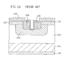
- FIG. 14 is a cross-sectional view illustrating the structure of a conventional accumulation-mode MISFET that uses a SiC substrate, i.e., a conventional double-implantation MISFET.
- the double-implantation MISFET includes: a SiC substrate 131 ; a high resistance SiC layer 132 provided on the SiC substrate 131 ; a p-well region 133 formed by implanting p-type dopant ions into a part of a surface region of the high resistance SiC layer 132 ; a channel layer 135 formed on upper surfaces of the p-well region 133 and the high resistance SiC layer 132 and containing n-type dopant; a source region 136 formed by implanting n-type dopant ions into parts of the channel layer 135 and the p-well region 133 ; a gate insulating film 137 formed of a thermal oxide film provided on a surface of the channel layer 135 ; a gate electrode 110 provided on the gate insulating film 137 ; a source electrode 138 that is provided on a wall surface of a groove passing through the source region 136 to reach the p-well region 133 , and that is formed so as to be
- the source region 136 and the high resistance SiC layer 132 are electrically connected with each other via the channel layer 135 that is also an n-type semiconductor layer. Furthermore, a portion of the channel layer 135 located in an upper part of the source region 136 is partially removed.
- the source electrode 138 , the source region 136 and the p-well region 133 are annealed so that they are in ohmic contact with each other.
- the SiC substrate 131 and the drain electrode 139 are in ohmic contact with each other.
- FIGS. 15A through 15E and FIGS. 16A through 16E are cross-sectional views illustrating process steps for fabricating a conventional double-implantation MISFET.
- a high resistance SiC layer 132 whose resistance is higher than that of the SiC substrate 131 (and whose dopant concentration is low) is epitaxially grown.
- p-type dopant ions are selectively implanted into a part of a surface region of the high resistance SiC layer 132 , thereby forming a p-well region 133 .
- annealing for activating the dopants that have been implanted thus far is performed. At this time, a surface of the p-well region 133 becomes rough.
- a channel layer 135 containing an n-type dopant is epitaxially grown on the surfaces of the p-well region 133 and the high resistance SiC layer 132 .
- n-type dopant ions are implanted into parts of the channel layer 135 and the p-well region 133 , thus forming a source region 136 that passes through the channel layer 135 to reach an inner portion of the p-well region 133 .
- the source region 136 and the high resistance SiC layer 132 are electrically connected via the channel layer 135 that is also an n-type semiconductor layer.
- annealing for activating the dopant implanted into the source region 136 is performed. At this time, surfaces of the channel layer 135 and the source region 136 become rough.
- a groove 134 that passes through the source region 136 to reach an upper portion of the p-well region 133 is formed, and then exposed surfaces of the channel layer 135 , the source region 136 and the p-well region 133 are thermally oxidized, thus providing a gate insulating film 137 formed of a thermal oxide film.
- portions of the gate insulating film 137 located on a wall surface of the groove 134 and around the groove 134 are removed.
- a source electrode 138 is formed on an exposed portion of the source region 136 from which the gate insulating film 137 has been removed. Further, a drain electrode 139 is formed on the backside of the SiC substrate 131 .
- a gate electrode 110 is formed on the gate insulating film 137 . Furthermore, annealing is performed so that the source electrode 138 , the source region 136 and the p-well region 133 are in ohmic contact with each other, and the SiC substrate 131 and the drain electrode 139 are in ohmic contact with each other.
- the channel layer 135 , the source region 136 and the high resistance SiC layer 132 are each formed by an n-type semiconductor layer; therefore, this MISFET is not an inversion-mode MISFET (i.e., a typical MISFET) that utilizes inversion of the channel layer, but an accumulation-mode MISFET that utilizes an accumulation state of the channel layer.
- an accumulation-mode MISFET having such a channel layer as compared with an inversion-mode MISFET, electric current flows to a deep region separated from an MIS interface; therefore, the accumulation-mode MISFET is unlikely to be influenced by a region in the vicinity of the MIS interface where interface state density is high, and thus channel mobility (carrier mobility) is improved.
- an off substrate whose principal surface is deviated and inclined from a nominal crystal plane (e.g., a (0001) plane) is used. This is because if such an off substrate is used, the high resistance SiC layer 132 is subjected to step flow growth when it is epitaxially grown, and thus the crystallinity of the high resistance SiC layer 132 is improved.
- a nominal crystal plane e.g., a (0001) plane
- an average surface roughness Ra prior to annealing is 1 nm or less; however, if activation annealing is performed at a temperature of 1700° C.
- the average surface roughness Ra becomes about 10 nm, which is ten times or more greater than that prior to the activation annealing (see, for example, Document 2 (Materials Science Forum Vols. 389-393, pp 831-834)).
- the step height of a macro step is as high as 50 nm or more, and thus a maximum surface roughness Rmax is 50 nm or more.
- the channel layer 135 is epitaxially grown on the surface of the well region 133 whose surface roughness is aggravated and whose smoothness is poor. Therefore, the surface roughness of the channel layer 135 is also aggravated, and thus the smoothness thereof is also poor.
- the channel layer 135 has an average surface roughness Ra of about 10 nm, and a maximum surface roughness Rmax of 50 nm or more.
- the channel layer 135 has been deposited, ion implantation for the source region 136 is carried out in the step shown in FIG. 15E , and activation annealing is carried out in the step shown in FIG. 16A ; therefore, the surface roughness of the channel layer 135 is further aggravated, and the smoothness thereof becomes poorer. Thus, the more the surface roughness is aggravated, the more the carrier mobility in the channel layer of the MISFET is reduced.
- the present inventors proposed a structure (stacked doped layer structure) in which an intentionally undoped first semiconductor layer, and a heavily doped and extremely thin second semiconductor layer ( ⁇ -doped layer) are alternately stacked, and we proved that a MISFET having the channel layer formed of such a stacked doped layer structure exhibits a considerably high carrier mobility (see Document 3 (Materials Science Forum Vols. 389-393, pp 1211-1214)).
- the second semiconductor layer ( ⁇ -doped layer) has to be extremely thinned such that the thickness thereof is about 10 nm, and thus the average surface roughness of the channel layer needs to be considerably reduced in accordance with the thickness of the second semiconductor layer. That is, the surface roughness of the channel layer has to be at least equal to or smaller than the thickness of the second semiconductor layer, and must be at least 10 nm or less. Moreover, in order to actually achieve a high functionality using a widegap semiconductor, the surface roughness of the channel layer is preferably 1 nm or less.
- the average surface roughness Ra refers to a centerline average roughness, and is defined by the JIS Standard as follows.
- dX ⁇ where a portion of a measured length L is extracted from a roughness curve in a centerline direction thereof, the X axis is taken in the centerline direction of the extracted portion, the Y axis is taken in the axial magnification direction (which is perpendicular to the X axis) of the extracted portion, and the roughness curve is represented by Y F(X).
- the present inventors found that if a large step such as step bunching exists at a surface of a channel layer, a thermal oxide film serving as a gate insulating film of a MISFET is thinned at the step portion, and the dielectric voltage of the oxide film is reduced in this portion.
- FIG. 17 is an SEM photograph showing the structure of an accumulation-mode double-implantation MISFET in the vicinity of its channel layer.
- the structure of this MISFET is substantially similar to that of the MISFET disclosed in Nonpatent Document 2.
- FIG. 17 three undoped layers each not subjected to intentional doping and having a thickness of 40 nm, and three doped layers each doped with an n-type dopant at a concentration of 5 ⁇ 10 17 cm ⁇ 3 and having a thickness of 10 nm are alternately stacked in an n-epitaxial layer (SiC) serving as the channel layer.
- the upper most portion of the channel layer is formed by the undoped layer having a thickness of 40 nm.
- a thermal oxide film is formed by dry oxidization that is performed at a temperature of 1180° C. for 3 hours.
- a p-well region is provided below the n-epitaxial layer, and Al ions are implanted so that the p-well region has a dopant concentration of 1 ⁇ 10 18 cm ⁇ 3 and a thickness of about 800 nm.
- activation annealing is carried out at a temperature of 1750° C. for 30 minutes.
- a step having a height of 50 nm or more is formed due to this activation annealing.
- a step having a height substantially similar to that of the step at the surface of the p-well region is also formed at the surface of the channel layer.
- the step does not rise perpendicularly, but forms a gentle slope.
- the thermal oxide film has a thickness of about 56 nm on a flat portion of the channel layer, and has a thickness of about 30 nm on a slope of the step, which is only a half of the thickness of the thermal oxide film on the flat portion. This is considered to be due to the fact that the flat portion and the step have different crystallographic plane orientations at their exposed surfaces, which varies the growth rate of the thermal oxide film.
- this MISFET since a leakage current flows through a thin portion of the thermal oxide film on the slope of the step, this MISFET has a gate dielectric breakdown voltage of 10 V or less; accordingly, a sufficient voltage cannot be applied to a gate, and thus a sufficient electric current cannot be obtained.
- the present invention has been made in view of the above-described problems, and its object is to provide a semiconductor device in which carrier mobility in a channel layer is high, and a method for fabricating the semiconductor device.
- An inventive semiconductor device is provided with an epitaxially grown layer on a silicon carbide layer including a high-concentration dopant diffused region; and a channel layer whose upper surface at a part of the epitaxially grown layer is smoother than that of the silicon carbide layer.
- the carrier mobility of the channel layer can be maintained at a high level. Further, even if the silicon carbide layer has a macro step due to step bunching, leakage current is small, and a high breakdown voltage is maintained because the upper surface of the channel layer is smooth.
- the semiconductor device may be further provided with an electrode that passes through the epitaxially grown layer to reach the high-concentration dopant diffused region.
- the semiconductor device having a high current drive capability can be easily obtained.
- an upper surface of the silicon carbide layer may be smoothed by polishing.
- the upper surface of the epitaxial grown layer i.e., the upper surface of the channel layer, is smoothed.
- the upper surface of the silicon carbide layer may be subjected to annealing with the silicon carbide layer covered with a carbon film.
- the need for a process such as polishing is eliminated, and practical application of the resulting device is facilitated.
- the lateral size of a region where the channel layer and the high-concentration dopant diffused layer are overlapped may be greater than the thickness of the channel layer. In such an embodiment, the supply of carriers from the high-concentration dopant diffused region to the channel layer is ensured.
- the average surface roughness of a surface of the silicon carbide layer in contact with the channel layer is preferably 2 nm or less.
- the average surface roughness of the upper surface of the channel layer is preferably 1 nm or less.
- the channel layer has a stacked doped layer structure.
- the semiconductor device with an extremely high carrier mobility is obtained.
- a high current drive capability is achieved if the above structure is employed in a vertical-type MISFET, a lateral-type MISFET and a lateral-type MESFET.
- annealing for activating a dopant which has been implanted into a high-concentration dopant diffused region formed in a part of a silicon carbide layer on a substrate, is carried out. Thereafter, an exposed surface of the silicon carbide layer including the high-concentration dopant diffused region is smoothed by CMP, mechanochemical polishing, dry etching or the like, and then a channel layer is formed on the silicon carbide layer including the high-concentration dopant diffused region.
- the surface of the silicon carbide layer including the high-concentration dopant diffused region becomes rough through the ion implantation and activation annealing.
- the channel layer is formed on the surface of the silicon carbide layer smoothed by the subsequent process, the surface of the channel layer is also smooth. Accordingly, the semiconductor device in which carrier mobility at the channel layer is high is obtained.
- a semiconductor device such as a MISFET or MESFET that uses a SiC substrate is provided with a channel layer whose surface is smooth, the semiconductor device having a high carrier mobility and a method for fabricating such a semiconductor device can be provided.
- FIG. 1 a cross-sectional view illustrating the structure of a double-implantation MISFET according to a first embodiment of the present invention.
- FIGS. 2A through 2F are cross-sectional views illustrating the first half of the process for fabricating the double-implantation MISFET of the first embodiment.
- FIGS. 3A through 3E are cross-sectional views illustrating the latter half of the process for fabricating the double-implantation MISFET of the first embodiment.
- FIGS. 4A and 4B are cross-sectional views showing a difference in the way a source region and a channel layer are overlapped between a conventional MISFET that uses a SiC substrate and an inventive MISFET.
- FIGS. 5A through 5F are cross-sectional views illustrating the first half of the process for fabricating a double-implantation MISFET according to a second embodiment of the present invention.
- FIGS. 6A through 6F are cross-sectional views illustrating the first half of the process for fabricating a double-implantation MISFET according to a third embodiment of the present invention.
- FIG. 7 is a cross-sectional view illustrating the structure of a MESFET that is a lateral-type transistor according to a fourth embodiment of the present invention.
- FIGS. 8A through 8E are cross-sectional views illustrating the first half of the process for fabricating a MESFET of the fourth embodiment.
- FIGS. 9A through 9C are cross-sectional views illustrating the latter half of the process for fabricating the MESFET of the fourth embodiment.
- FIG. 10 is a cross-sectional view illustrating the structure of a MESFET that is a lateral-type transistor according to a fifth embodiment of the present invention.
- FIGS. 11A and 11B are graphs showing the I-V characteristics of a vertical-type MISFET according to a reference example and a vertical-type MISFET according to the present embodiment.
- FIG. 12 is a graph showing the I-V characteristic of the vertical-type MISFET of the present embodiment.
- FIGS. 13A and 13B are graphs showing threshold voltage distributions in a lateral-type MISFET according to a reference example and a lateral-type MISFET according to the present embodiment.
- FIG. 14 is a cross-sectional view illustrating the structure of a conventional accumulation-mode MISFET that uses a SiC substrate, i.e., a conventional double-implantation MISFET.
- FIGS. 15A through 15E are cross-sectional views illustrating the first half of the process for fabricating the conventional double-implantation MISFET.
- FIGS. 16A through 16E are cross-sectional views illustrating the latter half of the process for fabricating the conventional double-implantation MISFET.
- FIG. 17 is an SEM photograph showing the structure of an accumulation-mode double-implantation MISFET in the vicinity of a channel layer, which is substantially similar to that of the MISFET disclosed in Nonpatent Document 2.
- FIG. 18 is a graph showing a correlation between an average surface roughness Ra of an underlying layer before epitaxial growth and an average surface roughness Ra of an epitaxially grown layer in the process for fabricating the double-implantation MISFET according to the second embodiment of the present invention.
- FIG. 1 is a cross-sectional view illustrating the structure of the double-implantation MISFET according to the first embodiment of the present invention.
- FIG. 1 shows only a partial cross-sectional structure of the MISFET, the planar structure thereof is similar to one disclosed in FIG. 2 or 10 of International Application PCT/JP01/07810, for example.
- the double-implantation MISFET includes: a low resistance SiC substrate 1 containing an n-type dopant at a concentration of 1 ⁇ 10 18 cm ⁇ 3 or more; a high resistance SiC layer 2 provided on a principal surface of the SiC substrate 1 and containing an n-type dopant at a concentration of about 1 ⁇ 10 15 cm ⁇ 3 to about 1 ⁇ 10 16 cm ⁇ 3 ; a p-well region 3 formed by doping a part of a surface region of the high resistance SiC layer 2 with a p-type dopant at a concentration of 1 ⁇ 10 16 cm ⁇ 3 to 1 ⁇ 10 18 cm ⁇ 3 ; a p+ contact region 4 formed by doping a part of the p-well region 3 with a p-type dopant at a concentration of about 5 ⁇ 10 19 cm ⁇ 3 ; a source region 6 formed by doping a part of the p-well region 3 with an n-type dopant at a concentration of about 1
- the cannel layer means a region of the epitaxially grown layer which is located underneath the gate electrode in a MISFET and means a region located between the source region and the drain region in a MESFET.
- a bias equal to or higher than a threshold voltage is applied to the gate electrode 10 with a predetermined voltage applied between the source electrode 8 and the drain electrode 9 , carriers are injected from the source electrode 8 into the channel layer 5 x through the source region 6 , and the carries travel from the channel layer 5 x to the drain electrode 9 through the high resistance SiC layer 2 and the SiC substrate 1 .
- the surfaces of the high resistance SiC layer 2 , the well region 3 and the source region 6 are smoothed, and the channel layer 5 x is epitaxially grown on these surfaces.
- the channel layer 5 x has a stacked doped layer structure formed by alternately stacking: a first semiconductor layer 5 a functioning as a carrier-traveling region; and a second semiconductor layer 5 b that is thinner than the first semiconductor layer 5 a and contains a high-concentration n-type dopant for enabling supply of carries to the first semiconductor layer 5 a .
- each first semiconductor layer 5 a has a dopant concentration of 1 ⁇ 10 16 cm ⁇ 3 or less and a thickness of about 40 nm
- each second semiconductor layer 5 b has a dopant concentration of about 1 ⁇ 10 17 cm ⁇ 3 to about 1 ⁇ 10 18 cm ⁇ 3 and a thickness of about 10 nm.
- the first and second semiconductor layers 5 a and 5 b are alternately deposited for three cycles with the first semiconductor layer 5 a formed as the lowermost layer of the channel layer 5 x , and the first semiconductor layer 5 a is further formed as the uppermost layer of the channel layer 5 x .
- the resulting channel layer 5 x has a thickness of 190 nm.
- a structure formed by alternately stacking: an undoped or not intentionally doped first semiconductor layer; and an extremely thin second semiconductor layer ( ⁇ -doped layer) doped at a high concentration, may be used.
- the source region 6 and the high resistance SiC layer 2 are electrically continuous via the channel layer 5 x that is also an n-type semiconductor layer.
- a portion of the channel layer 5 x located on a part of the source region 6 and the p+ contact region 4 is alloyed with Ni by annealing, thereby changing this portion into the source electrode 8 .
- the source electrode 8 is in ohmic contact with the source region 6 and the p+ contact region 4
- the drain electrode 9 is in ohmic contact with the SiC substrate 1 .
- FIGS. 2A through 2F and FIGS. 3A through 3E are cross-sectional views illustrating the process for fabricating the double-implantation MISFET of the first embodiment.
- a SiC substrate 1 that is an off substrate having an off angle of 8° from the (0001) plane of 4H—SiC is prepared, and a high resistance SiC layer 2 having an n-type dopant concentration lower than that of the SiC substrate 1 is epitaxially grown on a principal surface of the SiC substrate 1 by a thermal CVD or the like.
- silane (SiH 4 ) and propane (C 3 H 8 ) are used as a material gas
- hydrogen (H 2 ) is used as a carrier gas
- nitrogen (N 2 ) is used as a dopant gas.
- the high resistance SiC layer 2 preferably has a dopant concentration of 1 ⁇ 10 15 cm ⁇ 3 to 1 ⁇ 10 16 cm ⁇ 3 and a thickness of 10 ⁇ m or more.
- p-type dopant e.g., aluminum or boron
- p-type dopant e.g., aluminum or boron
- substrate temperature is kept at as high as 500° C.
- the p-well region 3 normally has a p-type dopant concentration of about 1 ⁇ 10 17 cm ⁇ 3 to about 1 ⁇ 10 18 cm ⁇ 3 and a depth of about 1 ⁇ m so as not to cause pinch-off.
- a p+ contact region 4 is formed by implanting high-concentration p-type dopant ions into a part of a surface region of the p-well region 3 .
- the p+ contact region 4 has a thickness of about 300 nm and a dopant concentration of about 5 ⁇ 10 19 cm ⁇ 3 or more.
- the ion implantation is performed in the same way as in the step of forming the p-well region 3 . Since activation annealing is performed at a time after the subsequent ion implantation for a source region 6 , no activation annealing is performed between the step shown in FIG. 2C and the step shown in FIG. 2D .
- n-type dopant ions are implanted into a part of the surface region of the p-well region 3 , thus forming the source region 6 .
- a silicon oxide film serving as an implantation mask and having a thickness of about 1 ⁇ m is deposited over the substrate, and then photolithography and dry etching are carried out to provide an opening only in a portion of the silicon oxide film which will form the source region 6 .
- nitrogen or phosphorus ions are implanted while the substrate temperature is kept at as high as 500° C. or more in order to reduce implantation defects.
- the silicon oxide film used as the mask is removed by hydrofluoric acid.
- the source region 6 has a dopant concentration of about 1 ⁇ 10 19 cm ⁇ 3 which is lower than the dopant concentration of the p+ contact region 4 . If the dopant concentration of the source region 6 is approximately similar to that of the p+ contact region 4 , the implantation mask for formation of the source region 6 has to cover the p+ contact region 4 . Furthermore, the source region 6 has a depth of about 300 nm, for example, which is shallower than that of the p+ contact region 4 .
- activation annealing is performed at 1700° C. for 30 minutes in an atmosphere of an inert gas such as argon.
- an inert gas such as argon.
- a macro step or a hillock is formed at exposed surfaces of the high resistance SiC layer 2 , the p-well region 3 , the p+ contact region 4 and the source region 6 , thus aggravating surface roughness and making surface smoothness poor.
- mechanochemical polishing for example, is performed to smooth the exposed surfaces of the high resistance SiC layer 2 , the p-well region 3 , the p+ contact region 4 and the source region 6 .
- the exposed surfaces are smoothed until an average surface roughness Ra of the surfaces becomes 2 nm or less, preferably 1 nm or less.
- chromium oxide for example, is used as abrasive grain.
- reactive ion etching or sacrificial oxidation is performed.
- both of the reactive ion etching and the sacrificial oxidation may be performed.
- a gas mixture of, for example, CF 4 and O 2 is used, and the reactive ion etching is carried out at a minimum sample bias voltage so as not to cause damage resulting from ion impact.
- sample bias potential can be suppressed to 1 V or less.
- the surfaces are very shallowly etched to a depth of 0.1 ⁇ m or less, for example, such that doping profile is not damaged.
- the substrate is placed in a quartz tube, for example, and is kept at 1180° C. for 90 minutes while dry oxygen is flowing at a flow rate of 1 (1/min), thus forming a thermal oxide film with a thickness of about 40 nm at the surface. Thereafter, the thermal oxide film is removed by hydrofluoric acid. In this step, the SiC layer 2 is removed at its surface to a depth of a few tens of nanometers. By changing the conditions of the thermal oxidation, the depth of a portion of the SiC layer 2 to be removed can be controlled.
- thermal CVD for example, is carried out to epitaxially grow an epitaxially grown layer 5 including a channel layer 5 x on the high resistance SiC layer 2 , the p-well region 3 , the source region 6 and the p+ contact region 4 .
- silane (SiH 4 ) and propane (C 3 H 8 ) are used as a material gas
- hydrogen (H 2 ) is used as a carrier gas
- nitrogen (N 2 ) is used as a dopant gas, for example.
- each first semiconductor layer 5 a see FIG.
- silane (SiH 4 ) and propane (C 3 H 8 ) are supplied as a material gas, and hydrogen (H 2 ) is supplied as a carrier gas, but a dopant gas is not supplied.
- hydrogen (H 2 ) is supplied as a carrier gas, but a dopant gas is not supplied.
- the surface of the epitaxially grown layer 5 (channel layer 5 x ), i.e., the stacked doped layer structure, is thermally oxidized, thus forming a silicon oxide film.
- the SiC substrate is placed in a quartz tube, for example, bubbling oxygen is introduced into the quartz tube at a flow rate of 2.5 (1/min), and thermal oxidation is carried out for 2.5 hours with the substrate temperature kept at 1180° C., thus forming the silicon oxide film that is a thermal oxide film having a thickness of about 60 nm.
- a drain electrode 9 formed of a nickel film with a thickness of 200 nm is formed on the backside of the SiC substrate 1 by a vapor deposition process. Annealing for the drain electrode 9 is performed after the subsequent formation of the source electrode 8 .
- a nickel film (Ni film) having a thickness of 200 nm is deposited over the substrate by vacuum deposition while the resist film Re is still remaining, and then a lift-off process is performed, thus allowing a nickel film 8 x serving as the source electrode 8 to remain.
- the Ni film 8 x is annealed at a temperature of 1000° C. for 2 minutes in an atmosphere of an inert gas such as nitrogen.
- an inert gas such as nitrogen.
- this annealing mutual diffusion and reaction of nickel (Ni) and silicon carbide (SiC) occur, thus forming the source electrode 8 that mainly consists of nickel silicide and passes through the epitaxially grown layer 5 to reach the source region 6 and the p+ contact region 4 .
- this annealing allows the drain electrode 9 to be in ohmic contact with the SiC substrate 1 .
- Annealing for allowing the source and drain electrodes 8 and 9 to be in ohmic contact with each other may be performed at the same time, or may be performed separately.
- a gate electrode 10 is formed at a position on the gate insulating film 7 located at a distance from the source electrode 8 .
- an aluminum film having a thickness of about 200 nm is deposited by vacuum deposition or the like, and then normal photolithography and etching are carried out to pattern the aluminum film, thus forming the gate electrode 10 .
- a silicon oxide film having a thickness of about 1 ⁇ m is deposited as an interlayer dielectric film that covers the source and gate electrodes 8 and 10 .
- RIE or the like is performed to form via holes that pass through the interlayer dielectric film and reach the source and gate electrodes 8 and 10
- an aluminum film having a thickness of about 2 ⁇ m is deposited by vacuum deposition or the like, and then normal photolithography and etching are carried out to pattern the aluminum film, thus forming electrode pads and/or interconnects.
- the double-implantation MISFET is completed.
- the thickness of the gate insulating film 7 is 50 nm to 65 nm, which is uniform in the range of about 10%.
- the breakdown voltage of the gate insulating film 7 is maintained at 40 V or more.
- the channel mobility of this MISFET is as high as 100 cm 2 /Vsec or more, the off-state breakdown voltage thereof is 600 V, and the on-state resistance thereof is 10 m ⁇ cm 2 or less.
- the surfaces of the underlying layers (which are the high resistance SiC layer 2 and the p-well region 3 in the present embodiment) are smoothed, and then the epitaxially grown layer 5 is epitaxially grown. Therefore, the irregularities that prevent travel of carriers in the channel layer 5 x can be reduced, and the carrier mobility can be maintained at a high level.
- the upper and lower surfaces of the channel layer 5 x are flat, carries are not dispersed when they travel, thus making it possible to increase the channel mobility and to reduce the on-state resistance.
- the channel layer 5 x has the stacked doped layer structure, in particular.
- the irregularities of the channel layer 5 x are greater than the thickness of the ⁇ -doped layer (which is the second semiconductor layer 5 b shown in FIG. 1 )
- the travel of carriers is adversely affected.
- the source region 6 is located below the channel layer 5 x , activation annealing does not have to be performed after the deposition of the channel layer 5 x , thus maintaining the surface smoothness after the deposition.
- the source region is formed after the deposition of the channel layer; therefore, activation annealing has to be performed prior to and subsequent to the step of carrying out epitaxial growth.
- activation annealing for ion-implanted regions can be performed at a time. That is, the present invention also achieves the advantage that the fabrication process can be simplified.
- the present embodiment carries out the above-described fabrication process to employ the structure in which the source region 6 and the channel layer 5 x overlap with each other.
- the contact area between the source region 6 and the channel layer 5 x can be increased, resulting in a reduction in contact resistance.
- FIGS. 4A and 4B are cross-sectional views showing a difference in the way the source region and the channel layer are overlapped between the conventional MISFET that uses a SiC substrate and the inventive MISFET.
- the source region 136 passes through the channel layer 135 ; therefore, the contact length between the source region 136 and the channel layer 135 in this cross section cannot be equal to or greater than the thickness t of the channel layer 135 (which is about 200 nm).
- the upper surface of the source region 6 and the lower surface of the channel layer 5 x are in contact with each other; therefore, the contact length A between the channel layer 5 x and the source region 6 in this cross section can be comparatively freely set.
- the contact length A in this cross section is preferably equal to or greater than the thickness of the channel layer 5 x .
- the contact length A is preferably 1 ⁇ m or more.
- the channel layer 5 x has the stacked doped layer structure in which the first and second semiconductor layers 5 a and 5 b having different concentrations are stacked.
- the entire channel layer may have a substantially uniform n-type dopant concentration.
- the n-type dopant concentration is preferably about 1 ⁇ 10 16 cm ⁇ 3 to about 5 ⁇ 10 17 cm ⁇ 3
- the thickness of the channel layer is preferably about 200 nm.
- no stacked doped layer structure is provided, and a channel layer having concentration distribution in which an n-type dopant concentration is varied in a depth direction may be provided.
- the present embodiment utilizes a chemical reaction between the metal film deposited on the surface of the epitaxially grown layer 5 (which is the Ni film in the present embodiment) and SiC without etching the epitaxially grown layer 5 , thereby forming the source electrode 8 that passes through the epitaxially grown layer 5 to reach the source region 6 . Therefore, the fabrication process can be considerably simplified, a reduction in fabrication cost can be achieved, and practical application of the resulting device is facilitated.
- mechanochemical polishing is performed as a process for smoothing surface irregularities created by annealing after ion implantation.
- isotropic dry etching may be performed in a plasma atmosphere using a gas containing a halogen element such as fluorine.
- abrasive grain directly contacts the surface, and a chemical. solution is used; therefore, contamination is likely to occur, and cleaning has to be carried out.
- dry etching that uses radicals is performed, contamination is unlikely to occur because the dry etching is a dry process.
- a so-called down-flow etching may be performed.
- a sample is separated from a plasma-generating chamber, for example, only neutral activated species (radicals) are transported to the sample, and etching is carried out by a chemical reaction between the activated species and the sample surface.
- etching is carried out by a chemical reaction between the activated species and the sample surface.
- contamination is unlikely to occur as long as an etching method that can set a sample bias independently of a bias for plasma generation as in ICP etching is employed so that the sample bias is set at a minimum level and ion energy is minimized.
- a gas containing a halogen element such as a gas mixture of CF 4 and O 2 , is used.
- the gate insulating film does not necessarily have to be a thermal oxide film.
- the gate insulating film may be a silicon oxide film deposited by CVD or the like.
- the gate insulating film may have a multilayer structure including a thermal oxide film and a deposition film.
- the gate insulating film does not have to be a silicon oxide film.
- the gate insulating film may be a metal oxide film such as a silicon nitride film, a silicon oxynitride film, a tantalum oxide film, or a hafnium oxide film.
- a semiconductor device has a structure apparently similar to that of the double-implantation MISFET in the first embodiment shown in FIG. 1 , and therefore, the structure of the MISFET according to the second embodiment is not shown.
- the MISFET of the present embodiment is greatly different from that of the first embodiment in that the surfaces of the high resistance SiC layer 2 , the well region 3 and the source region 6 are not smoothed, and the surface smoothness is maintained by activation annealing performed with the high resistance SiC layer 2 , the well region 3 and the source region 6 covered with a carbon film.
- the epitaxially grown layer 5 including the channel layer 5 x is epitaxially grown on the high resistance SiC layer 2 , the well region 3 and the source region 6 .
- the channel layer 5 x (the epitaxially grown layer 5 ) according to the present embodiment has an internal structure similar to that of the channel layer 5 x according to the first embodiment shown in FIG. 1 , and has the stacked doped layer structure as described in the first embodiment.
- FIGS. 5A through 5F are cross-sectional views illustrating the process for fabricating the double-implantation MISFET according to the second embodiment.
- the steps similar to those shown in FIGS. 2A through 2D are carried out.
- the high resistance SiC layer 2 is epitaxially grown on the principal surface of the SiC substrate 1 , and then ion implantation masks each of which is a hard mask are individually used so that the epitaxially grown high resistance SiC layer 2 is partially doped with a p-type dopant (such as aluminum or boron) by ion implantation to form the p-well region 3 , and the surface region of the p-well region 3 is partially doped with a high-concentration n-type dopant by ion implantation to form the source region 6 .
- a p-type dopant such as aluminum or boron
- a carbon film 55 is deposited on the high resistance SiC layer 2 , the well region 3 and the source region 6 .
- the carbon film 55 is deposited in the following manner. First, the SiC substrate 1 is placed at a substrate mounting part of a sputtering evaporation apparatus (not shown), and the evacuation of a chamber is carried out using a gas exhaust system. At this time, the degree of vacuum is approximately 10 ⁇ 4 Pa.
- an Ar gas is introduced, and an electric power of 100 W is applied to a target of a carbon plate at a pressure of about 10 ⁇ 2 Pa and a frequency as high as 13.56 MHz, thus carrying out sputtering evaporation.
- the carbon film 55 having a thickness of 50 nm is formed. It is confirmed that the content of components contained in the carbon film 55 , such as hydrogen other than carbon, is small, and the carbon film 55 has a carbon content of 99% or more.
- the SiC substrate 1 covered with the carbon film 55 is placed in an annealing apparatus (not shown), and a gas for anneal atmosphere is supplied through a gas supply system.
- a gas for anneal atmosphere an argon gas is selected.
- the flow rate of the argon gas is set at 0.5 l/min.
- the pressure within a chamber is kept constant at 91 kPa.
- the substrate temperature is increased to 1750° C., and annealing for activating the dopant, implanted into the high resistance SiC layer 2 , the well region 3 and the source region 6 , is carried out for 30 minutes while the substrate is maintained at this temperature.
- the application of high-frequency electric power to a coil is stopped to finish heating while the argon gas is still supplied, and the substrate is cooled down.
- the carbon film 55 is uniformly melted and removed using a solution of sulfuric acid and hydrogen peroxide water mixed at 3:1.
- the mixed solution hardly melts SiC layer 2 , and removes only the carbon film 55 .
- the SiC substrate is placed within a furnace for thermal oxidation in order to completely remove the carbon film 55 , and oxygen is supplied at a flow rate of 5 l/min and the substrate is heated to 800° C.
- oxygen is supplied at a flow rate of 5 l/min and the substrate is heated to 800° C.
- the carbon film 55 over the surface of the substrate is substantially completely removed by heating the substrate for 30 minutes, the heating is carried out for 60 minutes in the present embodiment.
- the percentage of activation of aluminum is 90% or more, meaning that the sufficient percentage of activation has been obtained.
- the average surface roughness Ra of the high resistance SiC layer 2 , the well region 3 and the source region 6 after the removal of the carbon film 55 is about 2 nm or less.
- the average surface roughness Ra is about 0.9 nm to about 1.3 nm. That is, less surface roughness is caused due to the activation annealing.
- the ion-implanted regions are covered with the carbon film 55 that is formed by the sputtering process, the surface roughness caused by sublimation of substance from the ion-implanted regions is suppressed. That is, the carbon film formed by the sputtering process has a high density, and is stable at a temperature as high as 1600° C., and therefore, the composition, structure and thickness of the carbon film substantially do not change. Accordingly, if the surfaces of the ion-implanted regions before the annealing are smooth, the smoothness of the surfaces of the ion-implanted regions can be maintained even after the annealing.
- the epitaxially grown layer 5 including the channel layer 5 x is epitaxially grown on the high resistance SiC layer 2 , the well region 3 and the source region 6 from which the carbon film 55 has been removed.
- the conditions of the epitaxial growth are similar to those described in the step shown in FIG. 3A according to the first embodiment.
- FIG. 18 is a graph showing the correlation between the average surface roughness Ra of the underlying layer before the epitaxial growth and the average surface roughness Ra of the epitaxially grown layer epitaxially grown thereon.
- the average surface roughness Ra of the underlying layer is 7 nm or more
- the average surface roughness Ra of the epitaxially grown layer epitaxially grown thereon is increased more than the average surface roughness Ra of the underlying layer.
- the average surface roughness Ra of the underlying layer is 2 nm or less
- the average surface roughness of the epitaxially grown layer epitaxially grown thereon is 1 nm or less, meaning that the epitaxially grown layer is smoothed.
- the semiconductor device has the source region (or source/drain region in the case of lateral-type MISFET and MESFET) as the underlying layer for epitaxial growth for formation of the channel layer, and the surface roughness of the channel layer after the epitaxial growth is smaller than that of the underlying layer. That is, the structural feature of each of the inventive vertical-type MISFET and the MESFET and lateral-type MISFET according to the aftermentioned embodiments is that the surface of the resulting device is smoother.
- the average surface roughness Ra of the underlying layers for epitaxial growth (which are the high resistance SiC layer 2 , the well region 3 and the source region 6 in the present embodiment) is 2 nm or less due to the dopant activation process with the carbon film being deposited, the average surface roughness Ra of the channel layer 5 x immediately after the epitaxial growth can be further reduced.
- Such a smoothing phenomenon in the epitaxial growth becomes conspicuous when the average surface roughness Ra of the underlying layers is about 1.5 nm or less.
- the average surface roughness Ra of the underlying layers does not necessarily have to be 1.5 nm or less.
- the MISFET of the present embodiment can achieve a high current drive capability, in particular.
- FIGS. 11A and 11B are graphs showing the I-V characteristics of a vertical-type MISFET according to a reference example and a vertical-type MISFET according to the present embodiment. It is to be noted that the data shown in FIG. 11A is not about the MISFET having the structure of the conventional MISFET shown in FIG. 14 , but about the MISFET whose basic shape is substantially similar to the structure shown in FIG. 14 . In this MISFET, after ion implantation for formation of the source region 136 has been performed, the source region is covered with a carbon film to perform dopant activation annealing, and the average surface roughness Ra of the channel layer 135 is about 1 nm.
- the average surface roughness Ra of the channel layer 5 x of the MISFET according to the present embodiment shown in FIG. 11B is about 0.1 nm.
- Each of the MISFETs has a gate length of 3 ⁇ m and a well spacing of 3 ⁇ m.
- FIGS. 11A and 11B if comparison is made using a common gate bias, it is seen that the current drive capability of the vertical-type MISFET according to the present embodiment is higher than that of the vertical-type MISFET according to the reference example. Since the current drive capability of the vertical-type MISFET according to the reference example is higher than that of the conventional vertical-type MISFET shown in FIG. 14 , the current drive capability of the vertical-type MISFET according to the present embodiment is considerably higher than that of the conventional vertical-type MISFET.
- FIG. 12 is a graph showing the I-V characteristic of the vertical-type MISFET of the present embodiment.
- the data shown in FIG. 12 is about a vertical-type MISFET including 9 cells (the actual vertical-type MISFET often includes about 1000 cells).
- the cell structure is the same as the sample with which the data shown in FIGS. 11A and 11B are obtained.
- an on-state resistance from the I-V characteristic shown in FIG. 12 , a value of 12 m ⁇ cm 2 is obtained. Since the on-state resistance of a vertical-type MISFET formed on a Si substrate is about 100 m ⁇ cm 2 , it is seen that the vertical MISFET of the present embodiment exhibits a high current drive capability and a low on-state resistance.
- the vertical-type MISFET of the present embodiment exhibits a high carrier mobility of 70 cm 2 /Vs, and a small threshold voltage variation.
- Epitaxial growth may be performed after the surfaces of the high resistance SiC layer 2 and the well region 3 have been smoothed by MCP as in the step shown in FIG. 2F according to the first embodiment. Even in such a case, the surface of the channel layer 5 x immediately after the epitaxial growth can be further smoothed.
- the fabrication method of the present embodiment is more advantageous than that of the first embodiment since the fabrication method of the present embodiment can further reduce the fabrication cost.
- FIGS. 6A through 6F are cross-sectional views illustrating the process for fabricating a double-implantation MISFET according to a third embodiment of the present invention.
- the step similar to that shown in FIG. 2A according to the first embodiment is carried out, thus epitaxially growing a high resistance SiC layer 2 on a principal surface of a SiC substrate 1 that is an off-substrate having an off angle of 8° from the (0001) plane of 4H—SiC.
- a p+ contact region 4 is formed by implanting high-concentration p-type dopant ions into a part of a surface region of the high resistance SiC layer 2 in order to allow a p-well region and a source electrode, which will be subsequently formed, to be in electrical contact with each other.
- the p+ contact region 4 has a dopant concentration of about 5 ⁇ 10 19 cm ⁇ 3 or more.
- the high resistance SiC layer 2 is partially doped with p-type dopant ions (such as aluminum or boron ions), thus forming the p-well region 3 .
- p-type dopant ions such as aluminum or boron ions
- a silicon oxide film 21 that serves as an implantation mask and has a thickness of about 3 ⁇ m is deposited on an upper surface of the high resistance SiC layer 2 , and only a portion of the silicon oxide film 21 where the p-well region 3 is to be formed is provided with an opening.
- aluminum (Al) or boron (B) ions are implanted while substrate temperature is kept at a high temperature of 500° C. or more in order to reduce implantation defects.
- the p-well region 3 normally has a p-type dopant concentration of about 1 ⁇ 10 17 cm ⁇ 3 to 1 ⁇ 10 18 cm ⁇ 3 and a depth of about 1 ⁇ m so as not to cause pinch-off.
- a polysilicon film for covering the silicon oxide film 21 (which has been used as the implantation mask), the well region 3 and the p+ contact region 4 is deposited, and the polysilicon film is subjected to selective and anisotropic etching, thus forming sidewalls 22 on side surfaces of the silicon oxide film 21 .
- a photolithography process is required, and a photo mask does not have to be used; therefore, a source region 6 will be formed to be self-aligned with the p-well region 3 .
- a surface region of the p-well region 3 is partially doped with a high-concentration n-type dopant by ion implantation, thus forming the source region 6 .
- nitrogen or phosphorus ions are implanted while the substrate is maintained at a temperature as high as 500° C. or more.
- the silicon oxide film 21 and the sidewalls 2 which have been used as a mask, are removed by selective dry etching or a process that uses hydrofluoric acid.
- the source region 6 has a dopant concentration of about 5 ⁇ 10 19 cm ⁇ 3 which is lower than that of p+ contact region 4 . Further, the depth of the source region 6 is shallower than that of the p+ contact region 4 , and is about 300 nm, for example.
- a carbon film 55 is deposited on the high resistance SiC layer 2 , the well region 3 and the source region 6 .
- the carbon film 55 is deposited in the following manner.
- the SiC substrate 1 is placed at a substrate mounting part of a sputtering evaporation apparatus not shown), and the evacuation of a chamber is carried out using a gas exhaust system. At this time, the degree of vacuum is approximately 10 ⁇ 4 Pa.
- an Ar gas is introduced, and an electric power of 100 W is applied to a target of a carbon plate at a pressure of about 10 ⁇ 2 Pa and a frequency as high as 13.56 MHz, thus carrying out sputtering evaporation.
- the carbon film 55 having a thickness of 50 nm is formed. It is confirmed that the content of components contained in the carbon film 55 , such as hydrogen other than carbon, is small, and the carbon film 55 has a carbon content of 99% or more.
- the SiC substrate 1 covered with the carbon film 55 is placed in an annealing apparatus (not shown), and a gas for anneal atmosphere is supplied through a gas supply system.
- a gas for anneal atmosphere an argon gas is selected.
- the flow rate of the argon gas is set at 0.5 l/min.
- the pressure within a chamber is kept constant at 91 kPa.
- the substrate temperature is increased to 1750° C., and annealing for activating the dopant, implanted into the high resistance SiC layer 2 , the well region 3 and the source region 6 , is carried out for 30 minutes while the substrate is maintained at this temperature.
- the application of high-frequency electric power to a coil is stopped to finish heating while the argon gas is still supplied, and the substrate is cooled down.
- the carbon film 55 is uniformly melted and removed using a solution of sulfuric acid and hydrogen peroxide water mixed at 3:1.
- the mixed solution hardly melts SiC layer 2 , and removes only the carbon film 55 .
- the SiC substrate is placed within a furnace for thermal oxidation in order to completely remove the carbon film 55 , and oxygen is supplied at a flow rate of 5 l/min and the substrate is heated to 800° C.
- oxygen is supplied at a flow rate of 5 l/min and the substrate is heated to 800° C.
- the carbon film 55 over the surface of the substrate is substantially completely removed by heating the substrate for 30 minutes, the heating is carried out for 60 minutes in the present embodiment.
- the percentage of activation of aluminum is 90% or more, meaning that the sufficient percentage of activation has been obtained.
- the average surface roughness Ra of the high resistance SiC layer 2 , the well region 3 and the source region 6 after the removal of the carbon film 55 is about 2 nm or less as in the second embodiment.
- the average surface roughness Ra is about 0.9 nm to about 1.3 nm. That is, no surface roughness is caused due to the activation annealing.
- the epitaxially grown layer 5 including the channel layer 5 x is epitaxially grown on the high resistance SiC layer 2 , the well region 3 and the source region 6 from which the carbon film 55 has been removed.
- the conditions of the epitaxial growth are similar to those described in the step shown in FIG. 3A according to the first embodiment.
- the average surface roughness Ra of the channel layer 5 x immediately after the epitaxial growth is about 0.08 nm to about 0.8 nm. That is, the surface roughness of the channel layer 5 x is smaller than that of the epitaxially grown underlying layers, thus causing a smoothing phenomenon in the epitaxial growth.
- the sidewalls 22 are formed on the side surfaces of the silicon oxide film 21 that is an implantation mask for the formation of the p-well region 3 , and then ion implantation for the formation of the source region 6 is carried out using the silicon oxide film 21 and the sidewalls 22 as an implantation mask. Therefore, since the source region 6 is formed so as to be self-aligned with the p-well region 3 , the width of the p-well region 3 in the cross section shown in FIG. 6E (i.e., the distance between the source region 6 and the high resistance SiC layer 2 ) becomes nearly constant, thus making the channel length substantially uniform. That is, the electrical characteristic of the MISFET that uses the SiC substrate is stabilized.
- FIG. 7 is a cross-sectional view illustrating the structure of a MESFET that is a lateral-type transistor according to a fourth embodiment of the present invention.
- the MESFET of the present embodiment includes: an intrinsic SiC substrate 41 that is an insulating substrate; an undoped high resistance SiC layer 42 epitaxially grown on the SiC substrate 41 ; source and drain regions 44 and 45 formed by doping each of two separate regions within the high resistance SiC layer 42 with an n-type dopant; an epitaxially grown layer 46 including a channel layer 46 x epitaxially grown on the high resistance SiC layer 42 ; a source electrode 49 formed of a Ni alloy film that passes through a portion of the channel layer 46 x , located above the source region 44 , to reach the source region 44 ; a drain electrode 50 formed of a Ni alloy film that passes through a portion of the channel layer 46 x , located above the drain region 45 , to reach the drain region 45 ; and a Schottky gate electrode 51 that is formed on a region of the channel layer 46 x located between the source electrode 49 and the drain electrode 50 .
- the channel layer 46 x has a stacked doped layer structure formed by alternately stacking: a first semiconductor layer 46 a functioning as a carrier-traveling region; and a second semiconductor layer 46 b that is thinner than the first semiconductor layer 46 a and contains a high-concentration n-type dopant for enabling supply of carries to the first semiconductor layer 46 a .
- each first semiconductor layer 46 a has a dopant concentration of 1 ⁇ 10 16 cm ⁇ 3 or less and a thickness of about 40 nm
- each second semiconductor layer 46 b has a dopant concentration of about 1 ⁇ 10 17 cm ⁇ 3 to about 1 ⁇ 10 18 cm ⁇ 3 and a thickness of about 10 nm.
- the first and second semiconductor layers 46 a and 46 b are alternately deposited for three cycles with the first semiconductor layer 46 a formed as the lowermost layer of the channel layer 46 x , and the first semiconductor layer 46 a is further formed as the uppermost layer of the channel layer 46 x .
- the resulting channel layer 46 x has a thickness of 190 nm.
- FIGS. 8A through 8E and FIGS. 9A through 9C are cross-sectional views illustrating the process for fabricating the MESFET of the present embodiment.
- thermal CVD or the like is performed to epitaxially grow an undoped high resistance SiC layer 42 on a principal surface of a SiC substrate 41 that is an off-substrate having an off angle of 8° from the (0001) plane of 4H—SiC.
- silane (SiH 4 ) and propane (C 3 H 8 ) are used as a material gas
- hydrogen (H 2 ) is used as a carrier gas.
- the high resistance SiC layer 42 preferably has a thickness of a few ⁇ m, for example.
- nitrogen or phosphorus ions as an n-type dopant are implanted into the separate regions of the high resistance SiC layer 42 , thus forming source and drain regions 44 and 45 .
- a CVD process is performed to deposit a silicon oxide film with a thickness of about 1 ⁇ m, which serves as an implantation mask, on the high resistance SiC layer 42 , and thereafter photolithography and dry etching are performed to form openings in portions of the silicon oxide film 43 located above the source and drain regions 44 and 45 .
- nitrogen or phosphorus ions are implanted while the substrate is maintained at a temperature as high as 500° C. in order to reduce implantation defects.
- the silicon oxide film 43 is removed by using hydrofluoric acid.
- the source and drain regions 44 and 45 normally have an n-type dopant concentration of 1 ⁇ 10 18 cm ⁇ 3 or more, and a depth of about 0.3 ⁇ m.
- activation annealing is performed at a temperature of 1750° C. for 30 minutes in an atmosphere of an inert gas such as argon, with a carbon film 55 deposited over the substrate.
- an inert gas such as argon
- the carbon film 55 is removed.
- a process that uses a solution of sulfuric acid and hydrogen peroxide water mixed at 3:1, and a heating process in a furnace for thermal oxidation are performed in the same way as in the step shown in FIG. 5F according to the second embodiment, and the conditions of the processes are the same as those in the step shown in FIG. 5F according to the second embodiment.
- the epitaxially grown layer 46 including the channel layer 46 x is epitaxially grown by thermal CVD, for example.
- the second semiconductor layer 46 b silane (SiH 4 ) and propane (C 3 H 8 ) are used as a material gas
- hydrogen (H 2 ) is used as a carrier gas
- nitrogen (N 2 ) is used as a dopant gas.
- each first semiconductor layer 46 a see FIG.
- silane (SiH 4 ) and propane (C 3 H 8 ) are used as a material gas, and hydrogen (H 2 ) is used as a carrier gas.
- hydrogen (H 2 ) is used as a carrier gas.
- the process similar to the shown in FIG. 3C according to the first embodiment is performed on a portion of the epitaxially grown layer 46 located on the source and drain regions 44 and 45 . More specifically, a lift-off process is performed using a resist film Re (not shown), thereby allowing Ni films 49 x and 50 x , each having a thickness of 200 nm, to remain over the substrate.
- the Ni films 49 x and 50 x will serve as source and drain electrodes 49 and 50 , respectively.
- the Ni films 49 x and 50 x are annealed at temperature of 1000° C. for 2 minutes in an atmosphere of an inert gas such as nitrogen. During this annealing, mutual diffusion and reaction of nickel (Ni) and silicon carbide (SiC) occur, thus forming the source and drain electrodes 49 and 50 mainly consisting of nickel silicide and passing through the channel layer 46 x to reach the source and drain regions 44 and 45 , respectively.
- an inert gas such as nitrogen.
- a Schottky gate electrode 51 is formed on a region located on the channel layer 46 x and between the source and drain electrodes 44 and 46 .
- a method for lifting off a nickel film for example, may be utilized.
- the thickness of the Schottky gate electrode 51 is preferably about 200 nm, for example.
- a silicon oxide film with a thickens of about 1 ⁇ m is deposited as an interlayer dielectric film that covers the source electrode 44 , the drain electrode 45 , the Schottky gate electrode 51 and the channel layer 46 x , and then RIE or the like is performed to form via holes that pass through the interlayer dielectric film and reach the source electrode 44 , the drain electrode 45 and the Schottky gate electrode 51 .
- an aluminum film with a thickness of about 2 ⁇ m is deposited by vacuum deposition or the like, and the aluminum film is patterned by normal photolithography and/or etching, thus forming electrode pads and/or interconnects.
- the MESFET with a high carrier mobility and a high current drive capability is obtained as in the second embodiment.
- the MESFET of the present embodiment since the channel layer 46 x has the stacked doped layer structure, the MESFET with a high breakdown voltage and a high current drive capability is obtained.
- the semiconductor device of the present embodiment is the MESFET having no gate insulating film.
- the semiconductor device is a lateral-type MISFET provided with: a gate insulating film located on the channel layer 46 x; and a gate electrode located on the gate insulating film, the effects similar to those of the first embodiment can be achieved.
- the MESFET or lateral-type MISFET according to the present embodiment may each be formed using not only a bulk SiC substrate, but also a SiC substrate that is obtained by epitaxially growing a SiC layer on, for example, a substrate made of various oxides.
- FIG. 10 is a cross-sectional view illustrating the structure of a MISFET that is a lateral-type transistor according to a fifth embodiment of the present invention.
- the MISFET of the present embodiment includes: a SiC substrate 61 containing a p-type dopant at a low concentration; an undoped high resistance SiC layer 62 epitaxially grown on the SiC substrate 61 and containing a p-type dopant at a concentration of about 1 ⁇ 10 15 cm ⁇ 3 to about 1 ⁇ 10 16 cm ⁇ 3 ; source and drain regions 64 and 65 formed by doping each of two separate regions within the high resistance SiC layer 62 with an n-type dopant; an epitaxially grown layer 66 including a channel layer 66 x epitaxially grown on the high resistance SiC layer 62 ; a source electrode 69 formed of a Ni alloy film that passes through a portion of the epitaxially grown layer 66 , located above the source region 64 , to reach the source region 64 ; a drain electrode 70 formed of a Ni alloy film that passes through a portion of the channel layer 66 x , located above the drain region 65 ,
- the channel layer 66 x has a stacked doped layer structure formed by alternately stacking: a first semiconductor layer 66 a functioning as a carrier-traveling region; and a second semiconductor layer 66 b that is thinner than the first semiconductor layer 66 a and contains a high-concentration n-type dopant for enabling supply of carries to the first semiconductor layer 66 a .
- each first semiconductor layer 66 a has a dopant concentration of 1 ⁇ 10 16 cm ⁇ 3 or less and a thickness of about 40 nm
- each second semiconductor layer 66 b has a dopant concentration of about 1 ⁇ 10 17 cm ⁇ 3 to about 1 ⁇ 10 18 cm ⁇ 3 and a thickness of about 10 nm.
- the first and second semiconductor layers 66 a and 66 b are alternately deposited for three cycles with the first semiconductor layer 66 a formed as the lowermost layer of the channel layer 66 x , and the first semiconductor layer 66 a is further formed as the uppermost layer of the channel layer 66 x .
- the resulting channel layer 66 x has a thickness of 190 nm.
- the fabrication method of the present embodiment is not shown and not described since the fabrication method of the present embodiment is basically similar to that of the fourth embodiment, except that the step of forming the gate insulating film 72 is added Since the surface of the channel layer 66 x is smoothed the lateral-type MISFET according to the present embodiment can achieve a high current drive capability and a high carrier mobility like the vertical-type MISFET according to the second embodiment. Besides, threshold voltage variations due to the production lot of the MISFETs and the positions thereof within a wafer are reduced.
- FIGS. 13A and 13B are graphs showing threshold voltage distributions in a lateral-type MISFET according to a reference example and a lateral-type MISFET according to the present embodiment.
- a channel layer is epitaxially grown, ion implantation for forming source/drain regions is carried out from above the channel layer, a carbon film is further deposited, and then dopant activation annealing is performed.
- the threshold voltage of the lateral-type MISFET according to the reference example is varied in the range of ⁇ 7.5 V to 5.0 V, whereas the threshold voltage of the lateral-type MISFET according to the present embodiment is concentratedly varied in the rage of 2.0 V to 4.5 V, and the present embodiment can achieve the lateral-type MISFET having a small threshold voltage variation.
- the carrier mobility of the lateral-type MISFET according to the present embodiment is 20 cm 2 /Vs, whereas that of the lateral-type MISFET according to the present embodiment is 70 cm 2 /Vs. That is, the carrier mobility of the lateral-type MISFET according to the present embodiment is more significantly improved than that of the lateral-type MISFET according to the present embodiment.
- the data shown in FIG. 13B is about the lateral-type MISFET, the similar data is obtained with regard to a vertical-type MISFET. Therefore, in the vertical-type MISFET, ion implantation for forming a source region is carried out; on the other hand, in the lateral-type MISFET and MESFET, ion implantation for forming source/drain regions is carried out. Thereafter, annealing for dopant activation is performed with a carbon film being deposited, the carbon film is then removed, and annealing for forming a channel layer is performed, thus obtaining the channel layer having a surface roughness smaller than that of an underlying layer for epitaxial growth. As a result, it becomes possible to obtain the vertical-type MISFET, the lateral-type MISFET or MESFET exhibiting a high current drive capability.
- the MISFET including the vertical-type MISFET and the lateral-type MISFET which has a small threshold voltage variation.
- the inventive semiconductor device and the fabrication method thereof can be utilized for a MISFET, MESFET or the like that uses a SiC substrate, which is particularly suitable for a power device or a high-frequency device.
Priority Applications (1)
| Application Number | Priority Date | Filing Date | Title |
|---|---|---|---|
| US12/338,395 US7846828B2 (en) | 2003-07-02 | 2008-12-18 | Semiconductor device and method for fabricating the same |
Applications Claiming Priority (2)
| Application Number | Priority Date | Filing Date | Title |
|---|---|---|---|
| JP2003-189980 | 2003-07-02 | ||
| JP2003189980 | 2003-07-02 |
Related Child Applications (1)
| Application Number | Title | Priority Date | Filing Date |
|---|---|---|---|
| US12/338,395 Division US7846828B2 (en) | 2003-07-02 | 2008-12-18 | Semiconductor device and method for fabricating the same |
Publications (2)
| Publication Number | Publication Date |
|---|---|
| US20050001217A1 US20050001217A1 (en) | 2005-01-06 |
| US7473929B2 true US7473929B2 (en) | 2009-01-06 |
Family
ID=33432317
Family Applications (2)
| Application Number | Title | Priority Date | Filing Date |
|---|---|---|---|
| US10/880,550 Active 2024-07-31 US7473929B2 (en) | 2003-07-02 | 2004-07-01 | Semiconductor device and method for fabricating the same |
| US12/338,395 Active 2024-11-02 US7846828B2 (en) | 2003-07-02 | 2008-12-18 | Semiconductor device and method for fabricating the same |
Family Applications After (1)
| Application Number | Title | Priority Date | Filing Date |
|---|---|---|---|
| US12/338,395 Active 2024-11-02 US7846828B2 (en) | 2003-07-02 | 2008-12-18 | Semiconductor device and method for fabricating the same |
Country Status (3)
| Country | Link |
|---|---|
| US (2) | US7473929B2 (zh) |
| EP (1) | EP1494268A3 (zh) |
| CN (1) | CN100481497C (zh) |
Cited By (12)
| Publication number | Priority date | Publication date | Assignee | Title |
|---|---|---|---|---|
| US20070287276A1 (en) * | 2006-06-08 | 2007-12-13 | Vladimir Frank Drobny | Unguarded schottky barrier diodes |
| US20090026497A1 (en) * | 2005-07-05 | 2009-01-29 | Nissan Motor Co., Ltd. | Method for Producing Semiconductor Device |
| US20090104762A1 (en) * | 2003-07-02 | 2009-04-23 | Panasonic Corporation | Semiconductor device and method for fabricating the same |
| US20100055858A1 (en) * | 2007-07-20 | 2010-03-04 | Masashi Hayashi | Silicon carbide semiconductor device and method for manufacturing the same |
| US20110223694A1 (en) * | 2010-03-09 | 2011-09-15 | Mitsubishi Electric Corporation | Method of manufacturing silicon carbide semiconductor device |
| US20130032797A1 (en) * | 2010-12-27 | 2013-02-07 | Koichi Hirano | Field-effect transistor and method for manufacturing the same |
| US20130244407A1 (en) * | 2008-02-15 | 2013-09-19 | Hitachi, Ltd. | Manufacturing method of semiconductor device |
| US20140183562A1 (en) * | 2012-11-09 | 2014-07-03 | Panasonic Corporation | Semiconductor device and method for fabricating the same |
| US9041049B2 (en) | 2011-02-01 | 2015-05-26 | Renesas Electronics Corporation | Power JFET |
| US20150287613A1 (en) * | 2014-04-04 | 2015-10-08 | Marko J. Tadjer | Basal plane dislocation elimination in 4h-sic by pulsed rapid thermal annealing |
| DE102015111891A1 (de) * | 2015-07-22 | 2017-01-26 | Infineon Technologies Ag | Verfahren zum Schützen einer Oberfläche eines Substrats und Halbleiterbauelement |
| US20230026927A1 (en) * | 2021-07-13 | 2023-01-26 | Showa Denko K.K. | SiC EPITAXIAL WAFER AND METHOD FOR MANUFACTURING SiC EPITAXIAL WAFER |
Families Citing this family (46)
| Publication number | Priority date | Publication date | Assignee | Title |
|---|---|---|---|---|
| EP1713117B1 (en) * | 2004-02-06 | 2011-01-19 | Panasonic Corporation | Process for producing a silicon carbide semiconductor device |
| DE112006000832B4 (de) * | 2005-04-06 | 2018-09-27 | Fairchild Semiconductor Corporation | Trenched-Gate-Feldeffekttransistoren und Verfahren zum Bilden derselben |
| US7528040B2 (en) * | 2005-05-24 | 2009-05-05 | Cree, Inc. | Methods of fabricating silicon carbide devices having smooth channels |
| US20070013012A1 (en) * | 2005-07-13 | 2007-01-18 | Taiwan Semiconductor Manufacturing Co., Ltd. | Etch-stop layer structure |
| US20070015373A1 (en) * | 2005-07-13 | 2007-01-18 | General Electric Company | Semiconductor device and method of processing a semiconductor substrate |
| JP5011493B2 (ja) | 2005-09-14 | 2012-08-29 | 関西電力株式会社 | 炭化珪素半導体素子の製造方法 |
| DE102006004870A1 (de) * | 2006-02-02 | 2007-08-16 | Siltronic Ag | Halbleiterschichtstruktur und Verfahren zur Herstellung einer Halbleiterschichtstruktur |
| US7700975B2 (en) * | 2006-03-31 | 2010-04-20 | Intel Corporation | Schottky barrier metal-germanium contact in metal-germanium-metal photodetectors |
| US20070235877A1 (en) * | 2006-03-31 | 2007-10-11 | Miriam Reshotko | Integration scheme for semiconductor photodetectors on an integrated circuit chip |
| US7781312B2 (en) * | 2006-12-13 | 2010-08-24 | General Electric Company | Silicon carbide devices and method of making |
| WO2008148095A1 (en) * | 2007-05-25 | 2008-12-04 | Astralux, Inc. | Hybrid silicon/non-silicon electronic device with heat spreader |
| JP4365894B2 (ja) * | 2007-08-07 | 2009-11-18 | パナソニック株式会社 | 炭化珪素半導体素子の製造方法 |
| CN101569015B (zh) * | 2007-10-15 | 2011-01-05 | 松下电器产业株式会社 | 半导体装置及其制造方法 |
| JP5518326B2 (ja) | 2008-12-26 | 2014-06-11 | 昭和電工株式会社 | 炭化珪素半導体装置の製造方法 |
| JP5438992B2 (ja) * | 2009-02-20 | 2014-03-12 | 昭和電工株式会社 | 炭化珪素半導体装置の製造方法 |
| CN102422396B (zh) | 2009-03-26 | 2014-07-02 | 佳能安内华股份有限公司 | 基板处理方法和结晶性碳化硅(sic)基板的制造方法 |
| KR20110133542A (ko) | 2009-03-27 | 2011-12-13 | 스미토모덴키고교가부시키가이샤 | Mosfet 및 mosfet의 제조 방법 |
| US8288220B2 (en) * | 2009-03-27 | 2012-10-16 | Cree, Inc. | Methods of forming semiconductor devices including epitaxial layers and related structures |
| CN102414818B (zh) | 2009-04-30 | 2013-03-20 | 松下电器产业株式会社 | 半导体元件、半导体装置及电力变换器 |
| WO2011027540A1 (ja) * | 2009-09-02 | 2011-03-10 | パナソニック株式会社 | 半導体素子およびその製造方法 |
| JP5443908B2 (ja) * | 2009-09-09 | 2014-03-19 | 株式会社東芝 | 半導体装置の製造方法 |
| CN102576723B (zh) | 2009-10-23 | 2014-09-24 | 松下电器产业株式会社 | 半导体装置及其制造方法 |
| WO2011061918A1 (ja) * | 2009-11-17 | 2011-05-26 | パナソニック株式会社 | 半導体素子及びその製造方法 |
| JP5601848B2 (ja) * | 2010-02-09 | 2014-10-08 | 三菱電機株式会社 | SiC半導体装置の製造方法 |
| WO2012032735A1 (ja) * | 2010-09-06 | 2012-03-15 | パナソニック株式会社 | 半導体装置およびその製造方法 |
| CN102468326B (zh) * | 2010-10-29 | 2015-01-07 | 中国科学院微电子研究所 | 接触电极制造方法和半导体器件 |
| EP2482315B1 (en) * | 2010-10-29 | 2015-08-12 | Panasonic Intellectual Property Management Co., Ltd. | Semiconductor element |
| WO2013035842A1 (ja) * | 2011-09-08 | 2013-03-14 | 株式会社タムラ製作所 | Ga2O3系半導体素子 |
| KR101603567B1 (ko) * | 2011-09-21 | 2016-03-15 | 미쓰비시덴키 가부시키가이샤 | 탄화 규소 반도체장치 및 그 제조방법 |
| JP5884357B2 (ja) * | 2011-09-22 | 2016-03-15 | 株式会社デンソー | 炭化珪素半導体装置 |
| WO2014068813A1 (ja) | 2012-10-30 | 2014-05-08 | パナソニック株式会社 | 半導体装置 |
| JP5802231B2 (ja) | 2013-03-22 | 2015-10-28 | 株式会社東芝 | 半導体装置及びその製造方法 |
| TWI626746B (zh) * | 2014-04-03 | 2018-06-11 | 財團法人工業技術研究院 | 半導體結構 |
| CN103928322B (zh) * | 2014-04-21 | 2016-08-17 | 西安电子科技大学 | 穿通型碳化硅绝缘栅双极型晶体管的制备方法 |
| CN104810293B (zh) * | 2015-03-27 | 2017-10-20 | 西安电子科技大学 | 分区复合栅结构SiC DMISFET器件的制作方法 |
| CN105140283A (zh) * | 2015-07-28 | 2015-12-09 | 国网智能电网研究院 | 一种碳化硅MOSFETs功率器件及其制作方法 |
| JP6406274B2 (ja) * | 2016-02-05 | 2018-10-17 | 株式会社デンソー | 半導体装置 |
| JPWO2017138247A1 (ja) * | 2016-02-10 | 2018-11-29 | 住友電気工業株式会社 | 炭化珪素エピタキシャル基板および炭化珪素半導体装置の製造方法 |
| JP6965499B2 (ja) * | 2016-03-16 | 2021-11-10 | 富士電機株式会社 | 炭化珪素半導体装置および炭化珪素半導体装置の製造方法 |
| JP2018082114A (ja) * | 2016-11-18 | 2018-05-24 | ルネサスエレクトロニクス株式会社 | 半導体装置の製造方法 |
| EP3358626B1 (en) * | 2017-02-02 | 2022-07-20 | Nxp B.V. | Method of making a semiconductor switch device |
| DE102017102127B4 (de) * | 2017-02-03 | 2023-03-09 | Infineon Technologies Ag | Verfahren zum Herstellen von Halbleitervorrichtungen unter Verwendung einer Epitaxie und Halbleitervorrichtungen mit einer lateralen Struktur |
| US10354922B1 (en) * | 2017-12-27 | 2019-07-16 | International Business Machines Corporation | Simplified block patterning with wet strippable hardmask for high-energy implantation |
| JP7113221B2 (ja) * | 2018-02-08 | 2022-08-05 | パナソニックIpマネジメント株式会社 | 炭化珪素半導体装置 |
| CN114335152B (zh) * | 2022-03-02 | 2022-05-24 | 江苏游隼微电子有限公司 | 一种碳化硅功率半导体器件及其制备方法 |
| CN117253784A (zh) * | 2023-11-15 | 2023-12-19 | 深圳天狼芯半导体有限公司 | 一种通过P离子注入钝化SiC MOS界面缺陷的方法 |
Citations (11)
| Publication number | Priority date | Publication date | Assignee | Title |
|---|---|---|---|---|
| US5753938A (en) * | 1996-08-08 | 1998-05-19 | North Carolina State University | Static-induction transistors having heterojunction gates and methods of forming same |
| US5977564A (en) * | 1996-10-16 | 1999-11-02 | Kabushiki Kaisha Toshiba | Semiconductor device |
| WO2000016382A1 (en) | 1998-09-16 | 2000-03-23 | Cree, Inc. | Low temperature formation of backside ohmic contacts for vertical devices |
| JP2001144288A (ja) | 1999-11-17 | 2001-05-25 | Denso Corp | 炭化珪素半導体装置 |
| US20020139992A1 (en) * | 2001-03-30 | 2002-10-03 | Rajesh Kumar | Silicon carbide semiconductor device and method of fabricating the same |
| US20020158251A1 (en) * | 2001-04-27 | 2002-10-31 | Kunimasa Takahashi | Semiconductor device and method for fabricating the same |
| WO2003028110A1 (fr) * | 2001-09-14 | 2003-04-03 | Matsushita Electric Industrial Co., Ltd. | Semi-conducteur |
| US6580125B2 (en) * | 2000-11-21 | 2003-06-17 | Matsushita Electric Industrial Co., Ltd. | Semiconductor device and method for fabricating the same |
| US20030137010A1 (en) * | 2000-07-25 | 2003-07-24 | Peter Friedrichs | Semiconductor construction with buried island region and contact region |
| US6617653B1 (en) * | 2000-05-31 | 2003-09-09 | Matsushita Electric Industrial Co., Ltd. | Misfet |
| WO2004008512A1 (ja) * | 2002-07-11 | 2004-01-22 | Matsushita Electric Industrial Co., Ltd. | 半導体装置及びその製造方法 |
Family Cites Families (9)
| Publication number | Priority date | Publication date | Assignee | Title |
|---|---|---|---|---|
| JPH11238742A (ja) * | 1998-02-23 | 1999-08-31 | Denso Corp | 炭化珪素半導体装置の製造方法 |
| JP3968860B2 (ja) * | 1998-03-20 | 2007-08-29 | 株式会社デンソー | 炭化珪素半導体装置の製造方法 |
| EP1114465B1 (de) | 1998-09-02 | 2007-03-21 | SiCED Electronics Development GmbH & Co KG | Halbleitervorrichtung mit ohmscher kontaktierung und verfahren zur ohmschen kontaktierung einer halbleitervorrichtung |
| DE19919905A1 (de) * | 1999-04-30 | 2000-11-02 | Siemens Ag | Halbleitervorrichtung mit ohmscher Kontaktierung und Verfahren zur ohmschen Kontaktierung einer Halbleitervorrichtung |
| US6884644B1 (en) * | 1998-09-16 | 2005-04-26 | Cree, Inc. | Low temperature formation of backside ohmic contacts for vertical devices |
| JP3760688B2 (ja) * | 1999-08-26 | 2006-03-29 | 富士電機ホールディングス株式会社 | 炭化けい素半導体素子の製造方法 |
| US6956238B2 (en) * | 2000-10-03 | 2005-10-18 | Cree, Inc. | Silicon carbide power metal-oxide semiconductor field effect transistors having a shorting channel and methods of fabricating silicon carbide metal-oxide semiconductor field effect transistors having a shorting channel |
| US7221010B2 (en) * | 2002-12-20 | 2007-05-22 | Cree, Inc. | Vertical JFET limited silicon carbide power metal-oxide semiconductor field effect transistors |
| US7473929B2 (en) * | 2003-07-02 | 2009-01-06 | Panasonic Corporation | Semiconductor device and method for fabricating the same |
-
2004
- 2004-07-01 US US10/880,550 patent/US7473929B2/en active Active
- 2004-07-02 EP EP04015637A patent/EP1494268A3/en not_active Withdrawn
- 2004-07-02 CN CNB2004100621855A patent/CN100481497C/zh active Active
-
2008
- 2008-12-18 US US12/338,395 patent/US7846828B2/en active Active
Patent Citations (13)
| Publication number | Priority date | Publication date | Assignee | Title |
|---|---|---|---|---|
| US5753938A (en) * | 1996-08-08 | 1998-05-19 | North Carolina State University | Static-induction transistors having heterojunction gates and methods of forming same |
| US5977564A (en) * | 1996-10-16 | 1999-11-02 | Kabushiki Kaisha Toshiba | Semiconductor device |
| WO2000016382A1 (en) | 1998-09-16 | 2000-03-23 | Cree, Inc. | Low temperature formation of backside ohmic contacts for vertical devices |
| JP2001144288A (ja) | 1999-11-17 | 2001-05-25 | Denso Corp | 炭化珪素半導体装置 |
| US6617653B1 (en) * | 2000-05-31 | 2003-09-09 | Matsushita Electric Industrial Co., Ltd. | Misfet |
| US20030137010A1 (en) * | 2000-07-25 | 2003-07-24 | Peter Friedrichs | Semiconductor construction with buried island region and contact region |
| US6580125B2 (en) * | 2000-11-21 | 2003-06-17 | Matsushita Electric Industrial Co., Ltd. | Semiconductor device and method for fabricating the same |
| US20020139992A1 (en) * | 2001-03-30 | 2002-10-03 | Rajesh Kumar | Silicon carbide semiconductor device and method of fabricating the same |
| US20020158251A1 (en) * | 2001-04-27 | 2002-10-31 | Kunimasa Takahashi | Semiconductor device and method for fabricating the same |
| WO2003028110A1 (fr) * | 2001-09-14 | 2003-04-03 | Matsushita Electric Industrial Co., Ltd. | Semi-conducteur |
| US20040051104A1 (en) * | 2001-09-14 | 2004-03-18 | Kenya Yamashita | Semiconductor device |
| WO2004008512A1 (ja) * | 2002-07-11 | 2004-01-22 | Matsushita Electric Industrial Co., Ltd. | 半導体装置及びその製造方法 |
| US20050173739A1 (en) * | 2002-07-11 | 2005-08-11 | Osamu Kusumoto | Semiconductor device and method for manufacturing same |
Non-Patent Citations (4)
| Title |
|---|
| "Schotty and Ohmic Contacts to SiC", Process Technology for Silicon Carbide Devices, p. 120, The Institute of Electrical Engineering. |
| A. Ohi et al., "Post-Implantation Annealing Effects on the Surface Morphology and Electrical Characteristics of 6H-SiC Implanted with Aluminum", Materials Science Forum, vol. 389-393, (2002), pp. 831-834. |
| O. Kusumoto et al., SiC Vertical DACFET (Vertical Delta-Doped Accumulation Channel MOSFET), Materials Science Forum, vol. 389-393, (2002), pp. 1211-1214. |
| Roccaforte, et al., "Ohmic Contacts to SiC", International Journal of High Speed Electronics and Systems, 2005, pp. 781-786. |
Cited By (23)
| Publication number | Priority date | Publication date | Assignee | Title |
|---|---|---|---|---|
| US20090104762A1 (en) * | 2003-07-02 | 2009-04-23 | Panasonic Corporation | Semiconductor device and method for fabricating the same |
| US7846828B2 (en) * | 2003-07-02 | 2010-12-07 | Panasonic Corporation | Semiconductor device and method for fabricating the same |
| US9048103B2 (en) * | 2005-07-05 | 2015-06-02 | Nissan Motor Co., Ltd. | Method for producing semiconductor device |
| US20090026497A1 (en) * | 2005-07-05 | 2009-01-29 | Nissan Motor Co., Ltd. | Method for Producing Semiconductor Device |
| US10535783B2 (en) | 2006-06-08 | 2020-01-14 | Texas Instruments Incorporated | Unguarded schottky barrier diodes |
| US8435873B2 (en) * | 2006-06-08 | 2013-05-07 | Texas Instruments Incorporated | Unguarded Schottky barrier diodes with dielectric underetch at silicide interface |
| US20070287276A1 (en) * | 2006-06-08 | 2007-12-13 | Vladimir Frank Drobny | Unguarded schottky barrier diodes |
| US20100055858A1 (en) * | 2007-07-20 | 2010-03-04 | Masashi Hayashi | Silicon carbide semiconductor device and method for manufacturing the same |
| US7829374B2 (en) * | 2007-07-20 | 2010-11-09 | Panasonic Corporation | Silicon carbide semiconductor device and method for manufacturing the same |
| US20130244407A1 (en) * | 2008-02-15 | 2013-09-19 | Hitachi, Ltd. | Manufacturing method of semiconductor device |
| US9449814B2 (en) * | 2008-02-15 | 2016-09-20 | Hitachi, Ltd. | Manufacturing method of semiconductor device |
| US20110223694A1 (en) * | 2010-03-09 | 2011-09-15 | Mitsubishi Electric Corporation | Method of manufacturing silicon carbide semiconductor device |
| US8084278B2 (en) * | 2010-03-09 | 2011-12-27 | Mitsubishi Electric Corporation | Method of manufacturing silicon carbide semiconductor device |
| US8871567B2 (en) * | 2010-12-27 | 2014-10-28 | Panasonic Corporation | Field-effect transistor and method for manufacturing the same |
| US20130032797A1 (en) * | 2010-12-27 | 2013-02-07 | Koichi Hirano | Field-effect transistor and method for manufacturing the same |
| US9041049B2 (en) | 2011-02-01 | 2015-05-26 | Renesas Electronics Corporation | Power JFET |
| US9543395B2 (en) | 2011-02-01 | 2017-01-10 | Renesas Electronics Corporation | Normally-off power JFET and manufacturing method thereof |
| US8847238B2 (en) * | 2012-11-09 | 2014-09-30 | Panasonic Corporation | Semiconductor device which can withstand high voltage or high current and method for fabricating the same |
| US20140183562A1 (en) * | 2012-11-09 | 2014-07-03 | Panasonic Corporation | Semiconductor device and method for fabricating the same |
| US20150287613A1 (en) * | 2014-04-04 | 2015-10-08 | Marko J. Tadjer | Basal plane dislocation elimination in 4h-sic by pulsed rapid thermal annealing |
| US10403509B2 (en) * | 2014-04-04 | 2019-09-03 | The Government Of The United States Of America, As Represented By The Secretary Of The Navy | Basal plane dislocation elimination in 4H—SiC by pulsed rapid thermal annealing |
| DE102015111891A1 (de) * | 2015-07-22 | 2017-01-26 | Infineon Technologies Ag | Verfahren zum Schützen einer Oberfläche eines Substrats und Halbleiterbauelement |
| US20230026927A1 (en) * | 2021-07-13 | 2023-01-26 | Showa Denko K.K. | SiC EPITAXIAL WAFER AND METHOD FOR MANUFACTURING SiC EPITAXIAL WAFER |
Also Published As
| Publication number | Publication date |
|---|---|
| US20050001217A1 (en) | 2005-01-06 |
| US7846828B2 (en) | 2010-12-07 |
| EP1494268A2 (en) | 2005-01-05 |
| EP1494268A3 (en) | 2010-04-21 |
| CN1577891A (zh) | 2005-02-09 |
| CN100481497C (zh) | 2009-04-22 |
| US20090104762A1 (en) | 2009-04-23 |
Similar Documents
| Publication | Publication Date | Title |
|---|---|---|
| US7473929B2 (en) | Semiconductor device and method for fabricating the same | |
| JP3784393B2 (ja) | 半導体装置及びその製造方法 | |
| US9559188B2 (en) | Trench gate type semiconductor device and method of producing the same | |
| US8564060B2 (en) | Semiconductor device with large blocking voltage and manufacturing method thereof | |
| EP1450394B1 (en) | Semiconductor device and method for manufacturing same | |
| US10263082B2 (en) | Semiconductor device having a gate electrode formed inside a trench | |
| US7241694B2 (en) | Method for manufacturing semiconductor device having trench in silicon carbide semiconductor substrate | |
| EP0671056B1 (en) | Power mosfet in silicon carbide | |
| US7265388B2 (en) | Semiconductor device | |
| US7691711B2 (en) | Method for fabricating silicon carbide vertical MOSFET devices | |
| US8847238B2 (en) | Semiconductor device which can withstand high voltage or high current and method for fabricating the same | |
| US20100314626A1 (en) | Silicon carbide semiconductor device and method of manufacturing the same | |
| JP5774261B2 (ja) | 炭化シリコン自己整合エピタキシャルmosfetおよびその製造方法 | |
| JP2007115875A (ja) | 炭化珪素半導体装置およびその製造方法 | |
| EP1523032A2 (en) | Silicon carbide-oxide layered structure, production method thereof, and semiconductor device | |
| JP2002329670A (ja) | 半導体装置及びその製造方法 | |
| JP2006066439A (ja) | 半導体装置およびその製造方法 | |
| JP2003234301A (ja) | 半導体基板、半導体素子及びその製造方法 | |
| JP4842527B2 (ja) | 半導体装置の製造方法 | |
| US9893162B2 (en) | Silicon carbide semiconductor device and method of manufacturing silicon carbide semiconductor device | |
| US20090159896A1 (en) | Silicon carbide mosfet devices and methods of making | |
| JP2011091125A (ja) | 炭化珪素半導体装置及びその製造方法 | |
| JPH11274481A (ja) | 炭化珪素半導体装置の製造方法 | |
| JP2008004726A (ja) | 半導体素子およびその製造方法 | |
| JP2020181967A (ja) | 炭化珪素半導体装置および炭化珪素半導体装置の製造方法 |
Legal Events
| Date | Code | Title | Description |
|---|---|---|---|
| AS | Assignment |
Owner name: MATSUSHITA ELECTRIC INDUSTRIAL CO., LTD., JAPAN Free format text: ASSIGNMENT OF ASSIGNORS INTEREST;ASSIGNORS:KUSUMOTO, OSAMU;KITABATAKE, MAKOTO;UCHIDA, MASAO;AND OTHERS;REEL/FRAME:015547/0076 Effective date: 20040628 |
|
| AS | Assignment |
Owner name: PANASONIC CORPORATION, JAPAN Free format text: CHANGE OF NAME;ASSIGNOR:MATSUSHITA ELECTRIC INDUSTRIAL CO., LTD.;REEL/FRAME:021897/0653 Effective date: 20081001 Owner name: PANASONIC CORPORATION,JAPAN Free format text: CHANGE OF NAME;ASSIGNOR:MATSUSHITA ELECTRIC INDUSTRIAL CO., LTD.;REEL/FRAME:021897/0653 Effective date: 20081001 |
|
| FEPP | Fee payment procedure |
Free format text: PAYOR NUMBER ASSIGNED (ORIGINAL EVENT CODE: ASPN); ENTITY STATUS OF PATENT OWNER: LARGE ENTITY |
|
| STCF | Information on status: patent grant |
Free format text: PATENTED CASE |
|
| FPAY | Fee payment |
Year of fee payment: 4 |
|
| FEPP | Fee payment procedure |
Free format text: PAYOR NUMBER ASSIGNED (ORIGINAL EVENT CODE: ASPN); ENTITY STATUS OF PATENT OWNER: LARGE ENTITY Free format text: PAYER NUMBER DE-ASSIGNED (ORIGINAL EVENT CODE: RMPN); ENTITY STATUS OF PATENT OWNER: LARGE ENTITY |
|
| FPAY | Fee payment |
Year of fee payment: 8 |
|
| MAFP | Maintenance fee payment |
Free format text: PAYMENT OF MAINTENANCE FEE, 12TH YEAR, LARGE ENTITY (ORIGINAL EVENT CODE: M1553); ENTITY STATUS OF PATENT OWNER: LARGE ENTITY Year of fee payment: 12 |