US7281180B2 - Memory system and test method therefor - Google Patents
Memory system and test method therefor Download PDFInfo
- Publication number
- US7281180B2 US7281180B2 US11/173,735 US17373505A US7281180B2 US 7281180 B2 US7281180 B2 US 7281180B2 US 17373505 A US17373505 A US 17373505A US 7281180 B2 US7281180 B2 US 7281180B2
- Authority
- US
- United States
- Prior art keywords
- data
- section
- memory
- write
- signal
- Prior art date
- Legal status (The legal status is an assumption and is not a legal conclusion. Google has not performed a legal analysis and makes no representation as to the accuracy of the status listed.)
- Expired - Fee Related, expires
Links
Images


Classifications
-
- G—PHYSICS
- G11—INFORMATION STORAGE
- G11C—STATIC STORES
- G11C29/00—Checking stores for correct operation ; Subsequent repair; Testing stores during standby or offline operation
- G11C29/04—Detection or location of defective memory elements, e.g. cell constructio details, timing of test signals
- G11C29/08—Functional testing, e.g. testing during refresh, power-on self testing [POST] or distributed testing
- G11C29/12—Built-in arrangements for testing, e.g. built-in self testing [BIST] or interconnection details
- G11C29/14—Implementation of control logic, e.g. test mode decoders
-
- G—PHYSICS
- G11—INFORMATION STORAGE
- G11C—STATIC STORES
- G11C29/00—Checking stores for correct operation ; Subsequent repair; Testing stores during standby or offline operation
- G11C29/02—Detection or location of defective auxiliary circuits, e.g. defective refresh counters
Definitions
- the present invention relates to an access operation test for a memory section in a memory system, and more particularly to an access operation test for a memory section in the case of access operations which take a longer time than the operation speed of the memory system.
- Patent Document 1 Japanese Kokai Publication No. 2001-256213
- a switch section 630 connects change terminal 630 a and change terminal 630 b , and an erase voltage supply end 249 is set to a ground potential.
- Erase pulse signal ERSM supplied from input terminal 620 is outputted to signal output pad P 1 by way of buffer 628 , and erase pulse signal ERSM can be externally detected.
- the erase operation is checked to determine if correct or not, by checking if erase pulse signal ERSM is outputted or not outputted from the memory cell subject to be erased to the outside of the microcomputer by way of signal output pads P 1 to Pn.
- a semiconductor memory IC disclosed in Japanese Kokai Publication No. H5-198200 (“Patent Document 2”) comprises, as shown in FIG. 15 , memory cells A 1 , A 2 ; signal lines L 1 , L 3 for writing data D 1 , D 3 into memory cells A 1 , A 2 , respectively; signal lines L 5 , L 6 for reading out memory data D 5 , D 6 ; signal lines L 2 , L 4 branched from the signal lines L 5 , L 6 ; selectors S 1 , S 2 for selecting data D 1 or D 5 and data D 3 or D 6 , respectively; correction circuit C for receiving signals D 7 , D 8 outputted from selectors S 1 , S 2 ; and signal line L 9 for outputting correction circuit signal D 9 from correction circuit C.
- the selectors S 1 , S 2 are set to select input data D 1 , D 3 during a test mode.
- correction circuit C insures that data D 9 is the normal data and is outputted without correction.
- correction circuit C insures that corrected normal data D 1 R is outputted on signal line L 9 .
- the test mode of the correction circuit C by directly selecting input data and supplying it from the correction circuit C, data writing or reading in the memory cell is not required, and, thus, the test time is shortened.
- Patent Document 3 operation of each address can be checked by comparing the address data of the input address signal and the output address data from address shift register 100 .
- data signals outputted from external signal input and output pads 103 , 104 to bus wirings 143 , 144 by way of wirings 123 , 124 and logic section 1000 are stored in data shift register 200 through wirings 153 , 154 .
- the data signals stored in the data shift register 200 are serially outputted therefrom to pad 107 as write data by way of data output line 127 .
- a counter 300 is used in place of a memory cell, and the operation is checked.
- the counter 300 is initialized, and predetermined data is preset in the counter 300 .
- a clock signal is entered in the counter 300 from clock pad 108 by way of clock line 128 , and the data signal of the data preset in the counter 300 is outputted from the counter 300 .
- the logic section 1000 takes in the data signal outputted from the counter 300 , and outputs it to pads 103 , 104 . When the data of the data signal outputted to the pads 103 , 104 and the data set in the counter 300 are equal to each other, the operation of this data line is normal.
- Patent Document 3 the operation of the logic section is tested without operating the memory section 3000 .
- exclusive test circuits are necessary for confirming normal address input or normal data input, or generating expectation value data for data output, and the circuit configuration is complicated and the chip size is increased.
- routing is different from propagation routing of address and data during normal operation. As a specific operation may occur in testing, the circuit in the memory section cannot be tested.
- the present invention is devised to solve at least one of the problems of the prior art, and it is hence an object of the present invention to present a memory system capable of checking the internal control operation of a memory control section or a memory section, and checking the wiring of each signal route, in simple configuration and procedure not accompanied by an increase in chip size and without requiring a data writing operation into the memory cell when testing the access operation of writing or reading in the memory section by control of the memory control section and its test method.
- the memory system of the present invention comprises a memory control section for providing a data write instruction and a memory section for storing and providing data in response to the memory control section, the memory section comprising a data output section for providing data to the memory control section upon recognition of the data write instruction during test.
- the data output section outputs the input data toward the memory control section.
- the test method of a memory system in accordance with the present invention is a test method of a memory system comprising a memory control section for providing a data write instruction and a memory section for storing and providing data in response to the memory control section.
- the data is outputted to the memory control section upon recognition of the data write instruction.
- the input data is outputted toward the memory control section.
- test time for a write instruction can be shortened.
- the test time for a write instruction can be shortened in the memory system having the memory section taking a long time in the write operation of data into the memory cell.
- the invention thus, provides a memory system capable of checking the generation of an access command in a memory control section, internal control operation of the memory section in regards to an access command input, and wiring of signal routes of access commands and data in a simple configuration and procedure not requiring an increase in chip size, when testing the access operation of writing or the like in the memory section by control of the memory control section.
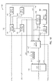
- FIG. 1 is a block diagram showing a first embodiment of the present invention.
- FIG. 2 is a circuit block diagram showing a memory section in accordance with the first embodiment of FIG. 1 .
- FIG. 3 is a circuit example of test circuit in accordance with the first embodiment of FIG. 1 .
- FIG. 4 is an operation waveform showing a test procedure in accordance with the first embodiment of FIG. 1 .
- FIG. 5 is a block diagram showing a second embodiment of the present invention.
- FIG. 6 is a circuit block diagram showing a memory section in accordance with the second embodiment of FIG. 5 .
- FIG. 7 is a circuit example of test circuit in accordance with the second embodiment of FIG. 5 .
- FIG. 8 is an operation waveform showing a test procedure in accordance with the second embodiment of FIG. 5 .
- FIG. 9 is a block diagram showing a third embodiment of the present invention.
- FIG. 10 is a circuit block diagram showing a memory section in accordance with the third embodiment of FIG. 9 .
- FIG. 11 is an operation waveform showing a test procedure in accordance with the third embodiment of FIG. 9 .
- FIG. 12 is a diagram showing a measure for reducing current consumption when not testing in a data/address register.
- FIG. 13 is a diagram showing a measure for reducing current consumption when not testing in a comparator.
- FIG. 14 is a conventional circuit diagram in accordance with Japanese Kokai Publication No. 2001-256213.
- FIG. 15 is a conventional circuit block diagram in accordance with Japanese Kokai Publication No. H5-198200.
- FIG. 16 is a conventional circuit block diagram in accordance with Japanese Kokai Publication No. H11-101858.
- FIG. 1 to FIG. 4 refer to a first embodiment of the present invention
- FIG. 5 to FIG. 8 refer to a second embodiment of the present invention
- FIG. 9 to FIG. 11 refer to a third embodiment of the present invention
- FIG. 12 and FIG. 13 refer to an embodiment of the present invention depicting reduction of current consumption when not testing.
- FIG. 1 is a block diagram showing a first embodiment of the present invention.
- a memory system 1 A comprises a memory section 2 A and a memory control section 3 A.
- the memory control section 3 A sends out access command CMD and data DI to the memory section 2 A, and receives output data DO from the memory section 2 A.
- the memory section 2 A includes a memory core section 9 A for input and output of data DI/DMC in a memory cell array (not shown) depending on access command CMD, data DI/DMC, and an address signal (not shown).
- the data DI is inputted into the memory core section 9 A by way of an input route not shown.
- the memory section 2 A includes a test circuit 4 A, a data register 5 A, and a data output section 6 A.
- the test circuit 4 A is activated by test signal TEST and outputs a write inhibit signal WINH to the memory core section 9 A. It also receives a write instruction recognition signal WR outputted when the memory core section 9 A recognizes a write command. Further, a select signal S, inverted depending on presence or absence of write instruction recognition signal WR, is outputted to the data output section 6 A.
- data DI outputted from the memory control section 3 A is entered and held.
- the retained data DR is outputted to the data output section 6 A.
- the data output section 6 A receives the retained data DR outputted from the data register 5 A and the cell data DMC outputted from the memory core section 9 A, and selects either one depending on the select signal S outputted from the test circuit 4 A to output as output data DO to the memory control section 3 A.
- write inhibit signal WINH is outputted from the test circuit 4 A, and the write operation in a memory cell of memory core section 9 A is inhibited regardless of the write command.
- the memory control section 3 A outputs write command CMD and data DI.
- the data DI is held in the data register 5 A and the write command CMD is inputted to the memory core section 9 A.
- the command is decoded, and when it is recognized as write command CMD, a write instruction recognition signal WR is generated.
- the write instruction recognition signal WR is a control signal when taking in the data DI or writing into the memory cell in the memory core section 9 A. However, at the time of testing, writing into the memory cell is inhibited by the write inhibit signal WINH.
- the test circuit 4 A inverts the select signal on the basis of generation of the write instruction recognition signal WR. That is, the select signal S is inverted when the write command CMD outputted from the memory control section 3 A is a command transmitted to the memory core section 9 A in the memory section 2 A which, when decoded in the memory core section 9 A, is recognized to be a write command.
- the data output section 6 A usually selects cell data DMC to output as output data DO. Only when the select signal S is inverted, the output data DO is switched to the retained data DR. As a result, at the time of testing when the write command CMD is recognized, the data DI entered along with the write command CMD is outputted as output data DO without being written into the memory cell.
- FIG. 2 is a circuit block diagram of memory section 12 A in the first embodiment.
- a memory core section 19 A comprises a command decoder 21 A, a data input buffer 22 A, a write control circuit 24 A, a write circuit 25 A, a read circuit 27 A, and a memory cell array 28 A, and receives access command CMD and data DI from the memory control section not shown.
- the command decoder 21 A receives access command CMD, and the data input buffer 22 A receives data DI.
- Write signal W outputted from the command decoder 21 A is inputted into the write control circuit 24 A.
- Data uptake signal WR 1 is inputted into the data input buffer 22 A and test circuit 14 A.
- An output terminal of the data input buffer 22 A is connected to the write circuit 25 A and also connected to the data register 15 A, and uptake data DIN taken into the data input buffer 22 A is outputted to the write circuit 25 A and data register 15 A.
- An output terminal of the write control circuit 24 A is connected to a trigger terminal (T) of the write circuit 25 A and also connected to the test circuit 14 A.
- Write execute signal WR 2 outputted on the basis of the write signal W outputted from the command decoder 21 A is outputted into the write circuit 25 A and test circuit 14 A.
- An output terminal of the write circuit 25 A is connected to the memory cell array 28 A for executing the write operation of uptake data DIN into the memory cell array 28 A on the basis of the write execute signal WR 2 entered in the trigger terminal (T).
- the read circuit 27 A is connected to the memory cell array 28 A and outputs the cell data DMC of the memory cell to the data output section 16 A.
- the test circuit 14 A outputs write inhibit signal WINH and select signal S.
- the write inhibit signal WINH is put into an inhibit terminal (INH) of the write circuit 25 A.
- the select signal S is put into a select terminal (SEL) of the data output section 16 A.
- the data register 15 A outputs the held retained data DR to the data output section 16 A.
- the data output section 16 A selects either the retained data DR or the cell data DMC depending on the select signal S to output as output data DO.
- FIG. 3 A circuit example of the test circuit 14 A is shown in FIG. 3 .
- NOR gates G 1 , G 2 have their output terminals connected to the input terminals of each other, and the gate G 1 receives a write execute signal WR 2 while the gate G 2 receives a data uptake signal WR 1 , thereby together forming a flip-flop circuit.
- the gate G 2 receives an inverted signal of test signal TEST from the output of an inverter gate G 5 .
- An output terminal of the gate G 2 is the output terminal of the flip-flop circuit, and is inputted into a NAND gate G 3 , together with an in-phase signal of test signal TEST by way of inverter gates G 5 and G 6 .
- An output terminal of the gate G 3 is connected to an inverter gate G 4 which outputs the select signal S.
- An inverted signal of test signal TEST outputted from the gate G 5 serves as the reset signal of the flip-flop circuit.
- the signal level of the select signal S is also at low level. As the select signal S is low level, cell data DMC is selected as output data DO, and the data is outputted from the memory cell array 28 A ( FIG. 2 ) when not testing.
- the select signal S is set to a low level by the data uptake signal WR 1 generated in the first instance, out of the two internal signals generated by recognition of write command CMD, and then inverted to a high level by the write execute signal WR 2 .
- the data output section 16 A (FIG. 2 ) selects the cell data DMC and is controlled to select the retained data DR at a predetermined timing
- the predetermined timing is a preparation completion timing necessary for writing the uptake data into the memory cell after uptake of data into the data input buffer 22 A and is, for example, a start-up completion timing of a bias voltage source necessary for the writing of data.
- test procedure by the circuit block shown in FIG. 2 is further explained by the operation waveform in FIG. 4 .
- write data DA is set as data DI and write command WCMD is inputted into the memory section 19 A
- the write command WCMD is decoded by the command decoder 21 A, and the data uptake signal WR 1 and write signal W are activated to high level.
- write data DA is taken into the data input buffer 22 A.
- the write data DA taken into the data input buffer 22 A is also held in the data register 15 A as uptake data DIN, and write data DA is held as retained data DR and outputted to the write circuit 25 A.
- the select signal S is inverted to a low level. Then, since the cell data DMC is selected as output data DO, the write data DA will not be outputted.
- the write control circuit 24 A along with an input of write signal W, activates the write execute signal WR 2 to switch to a high level after a predetermined timing. After transition of write execute signal WR 2 to a high level, the select signal S is inverted to a high level. As a result, retained data DR is selected as output data DO and, along with activation of data uptake signal WR 1 , the write data DA held in the data register 15 A is outputted.
- the cell data DMC is outputted as output data DO and, by activation of write execute signal WR 2 , the write data DA is outputted.
- the timing of two recognition signals activated successively can be detected, and the time delay from generation of data uptake signal WR 1 to generation of write execute signal WR 2 can also be inspected. At the same time, it is also tested whether generation or propagation of write data is normal or not.
- the write command and data lines can be tested without actually writing the write data into the memory cell, thereby shortening the test time required.
- FIG. 5 is a block diagram showing a second embodiment of the present invention.
- a memory system 1 B comprises, similar to the memory system 1 A in the first embodiment of the present invention ( FIG. 1 ), a memory section 2 B and a memory control section 3 B.
- the memory control section 3 B sends out access command CMD and data DI to the memory section 2 B, and receives output data DO from the memory section 2 B.
- the memory control section 3 B sends out address signal ADD.
- the memory section 2 B includes a data register 5 B, a data output section 6 B, and a memory core section 9 B, which have the same structure and action as the data register 5 A, data output section 6 A, and memory core section 9 A of the memory section 2 A of FIG. 1 .
- the memory section 2 B further includes a test circuit 4 B instead of the test circuit 4 A, and also comprises an address register section 7 B and a comparator 8 B. Only the structure and action different from the memory section 2 A ( FIG. 1 ) are explained hereinbelow, and description of similar structure and action is omitted.
- the address register section 7 B receives and holds address signal ADD outputted from the memory control section 3 B on the basis of write instruction recognition signal WR. Retained address signal ADR is then outputted to the comparator 8 B.
- the comparator 8 B receives address signal ADD in addition to the retained address signal ADR, and compares the two signals. When the two signals coincide, a coincidence signal E is outputted to the test circuit 4 B.
- write inhibit signal WINH is outputted from the test circuit 4 B, and the write operation in a memory cell of memory core section 9 B is inhibited regardless of the write command CMD.
- writing command CMD, data DI and address signal ADD are input to the memory section 2 B by the memory control section 3 B.
- the data DI is held in the data register 5 B and the write command CMD is inputted into the memory core section 9 B.
- the command is decoded and, when it is recognized as write command CMD, a write instruction recognition signal WR is generated.
- the write instruction recognition signal WR is a control signal when taking in the data DI or writing into the memory cell in the memory core section 9 B and, at the time of testing, writing into the memory cell is inhibited by the write inhibit signal WINH.
- the test circuit 4 B changes the select signal S depending on coincidence or non-coincidence of the comparison result as indicated by comparison coincidence signal E outputted from the comparator 8 B. That is, the select signal S is inverted when the write command CMD outputted from the memory control section 3 B is a normal command, normally transmitted to the memory core section 9 B in the memory section 2 B, and normally decoded in the memory core 9 B and recognized to be a write command, and when the same address signal ADD outputted twice from the memory control section 3 B during the cycle of a write command and after is confirmed to be normally generated and propagated to the memory section 2 B.
- FIG. 6 is a circuit block diagram of memory section 12 B of the second embodiment.
- a data register 15 B, a data output section 16 B, and a memory core section 19 B, a command decoder 21 B, a data input buffer 22 B, a write control circuit 24 B, a write circuit 25 B, a read circuit 27 B, and a memory cell array 28 B have the same structure and action as the memory section 12 A ( FIG. 2 ) of the first embodiment.
- the memory section 12 B also includes a test circuit 14 B instead of the test circuit 14 A, and further comprises an address register section 17 B and a comparator 18 B. From the memory control section (not shown), access command CMD, data DI, and address signal ADD are received.
- the structure and action different from the memory section 12 A ( FIG. 2 ) are explained below, and description of the same structure and action is omitted.
- An output terminal of address input buffer 23 B is connected to the address decoder not shown, and is also connected to the address register section 17 B for outputting the uptake address signal AD received by the address input buffer 23 B to the address decoder and the address register section 17 B.
- the data uptake signal WR 1 outputted from the command decoder 21 B is inputted into the address register section 17 B and the test circuit 14 B, as well as the data input buffer 22 B.
- the write execute signal WR 2 outputted from the write control circuit 24 B is outputted to the test circuit 14 B and the write circuit 25 B, as in the first embodiment.
- the address register section 17 B outputs retained address ADR held on the basis of data uptake signal WR 1 to the comparator 18 B.
- the comparator 18 B also receives address signal ADD and compares both address signals. When coinciding as a result of the comparison, a coincidence signal E is outputted to the test circuit 14 B.
- FIG. 7 A circuit example of the test circuit 14 B in accordance with the second embodiment of the present invention is shown in FIG. 7 .
- a NAND gate G 7 having one more input terminal than the gate G 3 is provided. In the increased input terminal in the gate G 7 , the coincidence signal E outputted from the comparator 18 B is entered.
- this circuit in addition to the inversion operation of the select signal S depending on the comparison result of the address signal ADD entered before and after write operation explained in the description of FIG. 5 , this circuit inverts the select signal S by the data uptake signal WR 1 and write execute signal WR 2 , as the write command recognition signal explained in connection with FIG. 3 .
- test procedure by the circuit shown in FIG. 6 is further explained by the operation waveform in FIG. 8 .
- write data DA is set as data DI
- address signal ADD 1 is set as address signal ADD
- write command WCMD is put into the memory section 19 B
- the write command WCMD is decoded by the command decoder 21 B
- the data uptake signal WR 1 and write signal W are activated to a high level.
- the uptake address signal AD is held in the address register section 17 B, and address signal ADD 1 is held as retained address signal ADR.
- the comparator 18 B compares the address signal ADD and retained address signal ADR, both having the address signal ADD 1 of same value, and the coincidence signal E is activated to a high level but, as a result of activation of data uptake signal WR 1 , the output of the flip-flop circuit ( FIG. 7 ) of the test circuit 14 B becomes a low level and, hence, the select signal S becomes low level.
- comparison of address signal ADD and retained address signal ADR may be also executed by a signal of an address transition detector.
- write data DA is taken into the data input buffer 22 B.
- the write data DA taken into the data input buffer 22 B is held in the data register 15 B as uptake data DIN, and write data DA is held as retained data DR, and is outputted to the write circuit 25 B.
- the write control circuit 24 B activates the write execute signal WR 2 to a high level after a predetermined timing. After transition of write execute signal WR 2 to a high level, the select signal S is inverted to the high level on the condition that the address signal ADD is not transitional. As a result, retained data DR is selected as output data DO and, along with activation of data uptake signal WR 1 , the write data DA held in the data register 15 B is outputted.
- the address signal ADD is transitioned from the address signal ADD 1 to address signal ADD 2 .
- the retained address signal ADR is held in the address signal ADD 1 and, thus, an output of non-coincidence is outputted from the comparator 18 B.
- the coincidence signal E is set to a low level and the select signal S is also set to the low level. Further, when the address signal ADD 2 is transitioned to address signal ADD 1 , the result of comparison coincides.
- the coincidence signal E is activated to a high level and the select signal S is also changed to a high level. Detection of transition from address signal ADD 1 to address signal ADD 2 may also be executed by an address transition detector not shown.
- the cell data DMC By activation of data uptake signal WR 1 , the cell data DMC is outputted as output data DO, and by activation of write execute signal WR 2 , the write data DA is outputted. Further, by changing the address signal ADD to a value different from the retained address ADR, cell data DMC is outputted, and by returning the address signal ADD to the value of retained address signal ADR, the write data DA is outputted again.
- detection of data outputted as output data DO it is tested whether generation, propagation or recognition of write command WCMD is normal or not, whether generation or propagation of write data is normal or not, and whether generation or propagation of address signal is normal or not. In this case, as in the first embodiment, it is possible to detect the time delay from generation of data uptake signal WR 1 until generation of write execute signal WR 2 .
- a nonvolatile memory capable of rewriting electrically such as a flash memory
- FIG. 9 is a block diagram showing a third embodiment of the present invention.
- a memory system IC comprises, similar to the memory system 1 A of the first embodiment of the present invention ( FIG. 1 ), a memory section 2 C and a memory control section 3 C.
- the memory control section 3 C sends out access command CMD and data DI to the memory section 2 C, and receives output data DO from the memory section 2 C.
- the memory section 2 C includes a data output section 6 C similar to the data output section 6 A in the memory section 2 A, and has the same structure and action.
- the memory section 2 C further includes a test circuit 4 C instead of the test circuit 4 A, and also comprises a data register 5 C instead of the data register 5 A. Only the structure and action different from the memory section 2 A ( FIG. 1 ) are explained, and description of same structure and action is omitted.
- the data register 5 C receives and holds data DI outputted from the memory control section 3 C on the basis of write instruction recognition signal WR. Retained data DR is outputted to the data output section 6 C.
- write inhibit signal WINH is outputted from the test circuit 4 C, and the write operation in a memory cell of memory core section 9 C is inhibited regardless of the write command CMD.
- write command CMD and data DI, and successively read command CMD are output from the memory control section 3 C.
- the write command CMD is inputted into the memory core section 9 C, the command is decoded and, when it is recognized to be write command CMD, a write instruction recognition signal WR is generated.
- the data DI is held in the data register 5 C.
- the write instruction recognition signal WR is a control signal when taking in the data DI or writing into the memory cell in the memory core section 9 C and, at the time of testing, writing into the memory cell is inhibited by the write inhibit signal WINH.
- read command CMD is inputted into the memory core section 9 C.
- the command is decoded and, when it is recognized to be read command CMD, a read instruction recognition signal RR is generated.
- the read instruction recognition signal RR is outputted from the memory cell in the memory core section 9 C and is inputted to the test circuit 4 C.
- the test circuit 4 C inverts the select signal S on the basis of the write instruction recognition signal WR and read instruction recognition signal RR. That is, the select signal S is inverted when the write command CMD and read command CMD outputted from the memory control section 3 C are normal commands, normally transmitted to the memory core section 9 C in the memory section 2 C, normally decoded in the memory core section 9 C and, thus, recognized to be normal commands.
- FIG. 10 is a circuit block diagram of memory section 12 C in accordance with the third embodiment of the present invention.
- the data register 15 C, data output section 16 C, and memory core section 19 C, the data input buffer 22 C, write control circuit 24 C, write circuit 25 C, and memory cell array 28 C have the same structure and action as the memory section 12 A ( FIG. 2 ) of the first embodiment.
- the memory section 12 C includes a test circuit 14 C instead of the test circuit 14 A, and further comprises a command decoder 21 C for decoding the read command CMD instead of the command decoder 21 A, and further comprises a read control circuit 26 C.
- the memory section 12 C also comprises a read circuit 27 C controlled by a data output signal RR 1 instead of a read circuit 27 A. From the memory control section not shown, access command CMD and data DI are entered. The structure and action different from the memory section 12 A ( FIG. 2 ) are explained below, and description of the same structure and action is omitted.
- the data register 15 C has a similar structure as the data register 15 A ( FIG. 2 ).
- the data DI during a write cycle is directly controlled by write instruction recognition signal WR and is held, but in the configuration shown in FIG. 10 , the data uptake signal WR 1 controls the data input buffer 22 C and takes in the data DI.
- the taken in data DIN is held.
- the data DI can be held during the write cycle and the same action and effect of the third embodiment of the present invention can be obtained.
- write execute signal WR 2 outputted from the write control circuit 24 C is inputted to the write circuit 25 C.
- the data output signal RR 1 outputted from the read control circuit 26 C is inputted to the read circuit 27 C and is also inputted to the test circuit 14 C.
- the circuit of test circuit 14 C has a circuit configuration similar to that of the circuit ( FIG. 3 ) in accordance with the first embodiment.
- Data output signal RR 1 is entered as an input signal instead of the write execute signal WR 2 in the circuit of the first embodiment.
- the test procedure of the circuit block diagram shown in FIG. 10 is explained by the operation waveform of FIG. 11 .
- write data DA is set as data DI and write command WCMD is put into the memory section 19 C
- the write command WCMD is decoded by the command decoder 21 C and the data uptake signal WR 1 and write signal W are activated to a high level. Further, as the data uptake signal WR 1 is activated to a high level, the select data S outputted from the test circuit 14 C becomes low level.
- write data DA is taken into the data input buffer 22 C.
- the write data DA taken into the data input buffer 22 C is held in the data register 15 C as uptake data DIN and write data DA is held as retained data DR and is outputted toward the write circuit 25 C.
- the write control circuit 24 C along with input of write signal W, activates the write execute signal WR 2 to a high level after a predetermined timing.
- the write execute signal WR 2 at a high level triggers the write circuit 25 C.
- write inhibit signal WINH is outputted from the test circuit 14 C, write operation into memory cell array 28 C is not executed.
- read command RCMD is put into the memory section 19 C. Being decoded by the command decoder 21 C, the read signal R is activated to a high level.
- the read control circuit 26 C along with the input of the read signal R, activates the data output signal RR 1 to a high level.
- the data output signal RR 1 at a high level triggers the read circuit 27 C and is outputted toward the test circuit 14 C, and inverts the select signal S to a high level.
- the retained data DR is selected as output data DO and the write data DA held in the data register 15 C is outputted as write data DA.
- the cell data DMC is outputted as output data DO, and by activation of data output signal RR 1 , the write data DA is outputted.
- the write data DA is outputted.
- detection of data outputted as output data DO it is tested whether generation, propagation or recognition of write command WCMD and read command RCMD is normal or not, and whether generation or propagation of write data is normal or not.
- a nonvolatile memory capable of rewriting electrically such as flash memory
- the circuit for holding the data DI comprises the data register 15 A to 15 C, aside from the data input buffer 21 A to 21 C, but it may alternatively be defined as one function of the data input buffer 21 A to 21 C.
- the data input buffer 21 A to 21 C takes in the data DI and the data register 15 A to 15 C holds the data DIN statically as explained above, but the data register 15 A to 15 C may alternatively be configured to hold the data on the basis of the data uptake signal WR 1 .
- FIG. 12 and FIG. 13 schematically show a configuration for saving current consumption when not testing by activating the test circuit only when testing.
- FIG. 12 shows a case of activating the data register and address register by test signal TEST. By disposing the data register and address register separately from the data input buffer or address input buffer, these registers can be activated only when testing.
- FIG. 13 shows a configuration of activating the comparator by test signal TEST. Since the comparator is not necessary for access operation when not testing, it can be activated only when testing.
- a logic gate for receiving an enable signal By disposing a logic gate for receiving an enable signal, only when activating the test signal TEST in the case of testing, it may be defined to propagate a signal from the logic gate, or it may be composed to connect or disconnect the supply voltage or bias current/voltage directly by the test signal TEST.
- the data uptake signal WR 1 and write execute signal WR 2 are examples of write instruction recognition signal WR, and the data output signal RR 1 is an example of read instruction recognition signal RR.
- the test time associated with a write command can be shortened.
- first to third embodiments are intended to test independently, but optional tests may be combined and executed therewith.
- testing of the erase command can be similarly executed.
- known data is held preliminarily in a data register and when the erase command is decoded by the command decoder, the select signal S is changed over on the basis of a recognition signal showing that the erase command is recognized, so that the generation, propagation or recognition of the erase command can be tested in the memory system without waiting for completion of data erasure in the memory cell.
- the erase operation inhibit signal should be generated instead of the write inhibit signal, and the actual erase operation should be inhibited.
Applications Claiming Priority (1)
| Application Number | Priority Date | Filing Date | Title |
|---|---|---|---|
| PCT/JP2004/009414 WO2006003704A1 (ja) | 2004-07-02 | 2004-07-02 | メモリシステム、およびその試験方法 |
Related Parent Applications (1)
| Application Number | Title | Priority Date | Filing Date |
|---|---|---|---|
| PCT/JP2004/009414 Continuation WO2006003704A1 (ja) | 2004-07-02 | 2004-07-02 | メモリシステム、およびその試験方法 |
Publications (2)
| Publication Number | Publication Date |
|---|---|
| US20060002196A1 US20060002196A1 (en) | 2006-01-05 |
| US7281180B2 true US7281180B2 (en) | 2007-10-09 |
Family
ID=35782521
Family Applications (1)
| Application Number | Title | Priority Date | Filing Date |
|---|---|---|---|
| US11/173,735 Expired - Fee Related US7281180B2 (en) | 2004-07-02 | 2005-07-01 | Memory system and test method therefor |
Country Status (3)
| Country | Link |
|---|---|
| US (1) | US7281180B2 (ja) |
| JP (1) | JP4757196B2 (ja) |
| WO (1) | WO2006003704A1 (ja) |
Families Citing this family (1)
| Publication number | Priority date | Publication date | Assignee | Title |
|---|---|---|---|---|
| KR100738969B1 (ko) * | 2006-08-16 | 2007-07-12 | 주식회사 하이닉스반도체 | 반도체 메모리의 온-다이 터미네이션 제어 장치 및 방법 |
Citations (12)
| Publication number | Priority date | Publication date | Assignee | Title |
|---|---|---|---|---|
| JPH04148446A (ja) * | 1990-10-12 | 1992-05-21 | Nec Corp | 記憶装置 |
| JPH0554684A (ja) | 1991-08-29 | 1993-03-05 | Fujitsu Ltd | 半導体記憶装置 |
| JPH0587890A (ja) | 1991-09-30 | 1993-04-06 | Nec Corp | 半導体集積回路 |
| JPH05198200A (ja) | 1992-01-20 | 1993-08-06 | Nec Ic Microcomput Syst Ltd | 半導体メモリic |
| US5297029A (en) | 1991-12-19 | 1994-03-22 | Kabushiki Kaisha Toshiba | Semiconductor memory device |
| US5677913A (en) * | 1996-07-01 | 1997-10-14 | Sun Microsystems, Inc. | Method and apparatus for efficient self testing of on-chip memory |
| JPH11101858A (ja) | 1997-09-29 | 1999-04-13 | Toshiba Microelectronics Corp | 半導体集積回路 |
| JPH11272643A (ja) | 1998-03-26 | 1999-10-08 | Sanyo Electric Co Ltd | マイクロコンピュータ |
| JP2000346905A (ja) | 1999-06-04 | 2000-12-15 | Nec Corp | 半導体装置およびそのテスト方法 |
| US20010022744A1 (en) | 2000-03-10 | 2001-09-20 | Kabushiki Kaisha Toshiba | Semiconductor memory device having a page latch circuit and a test method thereof |
| JP2001256213A (ja) | 2000-03-09 | 2001-09-21 | Mitsubishi Electric Corp | マイクロコンピュータ |
| US6574763B1 (en) * | 1999-12-28 | 2003-06-03 | International Business Machines Corporation | Method and apparatus for semiconductor integrated circuit testing and burn-in |
Family Cites Families (1)
| Publication number | Priority date | Publication date | Assignee | Title |
|---|---|---|---|---|
| JPH05282882A (ja) * | 1991-12-19 | 1993-10-29 | Toshiba Corp | 不揮発性半導体メモリ |
-
2004
- 2004-07-02 WO PCT/JP2004/009414 patent/WO2006003704A1/ja active Application Filing
- 2004-07-02 JP JP2006527622A patent/JP4757196B2/ja not_active Expired - Fee Related
-
2005
- 2005-07-01 US US11/173,735 patent/US7281180B2/en not_active Expired - Fee Related
Patent Citations (12)
| Publication number | Priority date | Publication date | Assignee | Title |
|---|---|---|---|---|
| JPH04148446A (ja) * | 1990-10-12 | 1992-05-21 | Nec Corp | 記憶装置 |
| JPH0554684A (ja) | 1991-08-29 | 1993-03-05 | Fujitsu Ltd | 半導体記憶装置 |
| JPH0587890A (ja) | 1991-09-30 | 1993-04-06 | Nec Corp | 半導体集積回路 |
| US5297029A (en) | 1991-12-19 | 1994-03-22 | Kabushiki Kaisha Toshiba | Semiconductor memory device |
| JPH05198200A (ja) | 1992-01-20 | 1993-08-06 | Nec Ic Microcomput Syst Ltd | 半導体メモリic |
| US5677913A (en) * | 1996-07-01 | 1997-10-14 | Sun Microsystems, Inc. | Method and apparatus for efficient self testing of on-chip memory |
| JPH11101858A (ja) | 1997-09-29 | 1999-04-13 | Toshiba Microelectronics Corp | 半導体集積回路 |
| JPH11272643A (ja) | 1998-03-26 | 1999-10-08 | Sanyo Electric Co Ltd | マイクロコンピュータ |
| JP2000346905A (ja) | 1999-06-04 | 2000-12-15 | Nec Corp | 半導体装置およびそのテスト方法 |
| US6574763B1 (en) * | 1999-12-28 | 2003-06-03 | International Business Machines Corporation | Method and apparatus for semiconductor integrated circuit testing and burn-in |
| JP2001256213A (ja) | 2000-03-09 | 2001-09-21 | Mitsubishi Electric Corp | マイクロコンピュータ |
| US20010022744A1 (en) | 2000-03-10 | 2001-09-20 | Kabushiki Kaisha Toshiba | Semiconductor memory device having a page latch circuit and a test method thereof |
Non-Patent Citations (2)
| Title |
|---|
| "Automated Test Equipment for Research on Nonvolatile Memories" by Pellati et al. This paper appears in: IEEE Transactions on Instrumentation and Measurement, Publication Date: Oct. 2001 vol.: 50, Issue: 5 pp. 1162-1166 ISSN: 0018-9456 INSPEC Accession No.: 7164900. * |
| "Using Device ATE Testers to Solve Anomalies" by Swail This paper appears in: AUTOTESTCON Proceedings, 2002. IEEE Publication Date: 2002 pp.: 650-660 ISSN: 1080-7725 INSPEC Accession No.: 7597176. * |
Also Published As
| Publication number | Publication date |
|---|---|
| US20060002196A1 (en) | 2006-01-05 |
| JPWO2006003704A1 (ja) | 2008-07-31 |
| WO2006003704A1 (ja) | 2006-01-12 |
| JP4757196B2 (ja) | 2011-08-24 |
Similar Documents
| Publication | Publication Date | Title |
|---|---|---|
| KR100901404B1 (ko) | 패리티 셀 어레이를 구비한 메모리 회로 | |
| KR100217215B1 (ko) | 내장 기록 기능을 갖는 플래시 메모리를 끼워넣은 마이크로컴퓨터 | |
| KR101075091B1 (ko) | 반도체 메모리 장치 및 그 테스트 방법 | |
| US7508724B2 (en) | Circuit and method for testing multi-device systems | |
| US7414914B2 (en) | Semiconductor memory device | |
| US8605533B2 (en) | Apparatus and method for protecting data in flash memory | |
| KR100319733B1 (ko) | 불휘발성 반도체 메모리ic 및 그 번인 테스트 방법 | |
| US5659549A (en) | Memory test system having a pattern generator for a multi-bit test | |
| US6275428B1 (en) | Memory-embedded semiconductor integrated circuit device and method for testing same | |
| US20020188900A1 (en) | Test method and test system for semiconductor device | |
| US7257752B2 (en) | Circuit and method for performing built-in self test and computer readable recording medium for storing program thereof | |
| US7281180B2 (en) | Memory system and test method therefor | |
| US8055936B2 (en) | System and method for data recovery in a disabled integrated circuit | |
| JP3791956B2 (ja) | 不揮発性半導体記憶装置の検査方法 | |
| KR100632338B1 (ko) | 반도체 장치 및 그 시험 방법 | |
| KR100793221B1 (ko) | 반도체 장치 및 그 시험 방법 | |
| US6226753B1 (en) | Single chip integrated circuit with external bus interface | |
| JP2001243797A (ja) | 半導体装置及びその試験方法 | |
| JPH0263280B2 (ja) | ||
| JP4121594B2 (ja) | 不揮発メモリ内蔵マイクロコンピュータ | |
| US5307313A (en) | Flag circuit for memory | |
| JP3217548B2 (ja) | 半導体記憶装置 | |
| JPH08329698A (ja) | 半導体メモリ | |
| JP2001256213A (ja) | マイクロコンピュータ | |
| CN114822621A (zh) | 信号接收电路、存储器及控制方法 |
Legal Events
| Date | Code | Title | Description |
|---|---|---|---|
| AS | Assignment |
Owner name: SPANSION LLC, CALIFORNIA Free format text: ASSIGNMENT OF ASSIGNORS INTEREST;ASSIGNORS:FURUYAMA, TAKAAKI;KAWAMOTO, SATORU;REEL/FRAME:016756/0340;SIGNING DATES FROM 20050629 TO 20050630 |
|
| STCF | Information on status: patent grant |
Free format text: PATENTED CASE |
|
| AS | Assignment |
Owner name: BARCLAYS BANK PLC,NEW YORK Free format text: SECURITY AGREEMENT;ASSIGNORS:SPANSION LLC;SPANSION INC.;SPANSION TECHNOLOGY INC.;AND OTHERS;REEL/FRAME:024522/0338 Effective date: 20100510 Owner name: BARCLAYS BANK PLC, NEW YORK Free format text: SECURITY AGREEMENT;ASSIGNORS:SPANSION LLC;SPANSION INC.;SPANSION TECHNOLOGY INC.;AND OTHERS;REEL/FRAME:024522/0338 Effective date: 20100510 |
|
| FPAY | Fee payment |
Year of fee payment: 4 |
|
| AS | Assignment |
Owner name: SPANSION LLC, CALIFORNIA Free format text: RELEASE BY SECURED PARTY;ASSIGNOR:BARCLAYS BANK PLC;REEL/FRAME:035201/0159 Effective date: 20150312 Owner name: SPANSION TECHNOLOGY LLC, CALIFORNIA Free format text: RELEASE BY SECURED PARTY;ASSIGNOR:BARCLAYS BANK PLC;REEL/FRAME:035201/0159 Effective date: 20150312 Owner name: SPANSION INC., CALIFORNIA Free format text: RELEASE BY SECURED PARTY;ASSIGNOR:BARCLAYS BANK PLC;REEL/FRAME:035201/0159 Effective date: 20150312 |
|
| AS | Assignment |
Owner name: MORGAN STANLEY SENIOR FUNDING, INC., NEW YORK Free format text: SECURITY INTEREST;ASSIGNORS:CYPRESS SEMICONDUCTOR CORPORATION;SPANSION LLC;REEL/FRAME:035240/0429 Effective date: 20150312 |
|
| FPAY | Fee payment |
Year of fee payment: 8 |
|
| FPAY | Fee payment |
Year of fee payment: 8 |
|
| SULP | Surcharge for late payment |
Year of fee payment: 7 |
|
| AS | Assignment |
Owner name: CYPRESS SEMICONDUCTOR CORPORATION, CALIFORNIA Free format text: ASSIGNMENT OF ASSIGNORS INTEREST;ASSIGNOR:SPANSION, LLC;REEL/FRAME:036036/0738 Effective date: 20150601 |
|
| AS | Assignment |
Owner name: CYPRESS SEMICONDUCTOR CORPORATION, CALIFORNIA Free format text: PARTIAL RELEASE OF SECURITY INTEREST IN PATENTS;ASSIGNOR:MORGAN STANLEY SENIOR FUNDING, INC., AS COLLATERAL AGENT;REEL/FRAME:039708/0001 Effective date: 20160811 Owner name: SPANSION LLC, CALIFORNIA Free format text: PARTIAL RELEASE OF SECURITY INTEREST IN PATENTS;ASSIGNOR:MORGAN STANLEY SENIOR FUNDING, INC., AS COLLATERAL AGENT;REEL/FRAME:039708/0001 Effective date: 20160811 |
|
| FEPP | Fee payment procedure |
Free format text: PAYOR NUMBER ASSIGNED (ORIGINAL EVENT CODE: ASPN); ENTITY STATUS OF PATENT OWNER: LARGE ENTITY |
|
| AS | Assignment |
Owner name: MONTEREY RESEARCH, LLC, CALIFORNIA Free format text: ASSIGNMENT OF ASSIGNORS INTEREST;ASSIGNOR:CYPRESS SEMICONDUCTOR CORPORATION;REEL/FRAME:040911/0238 Effective date: 20160811 |
|
| FEPP | Fee payment procedure |
Free format text: MAINTENANCE FEE REMINDER MAILED (ORIGINAL EVENT CODE: REM.); ENTITY STATUS OF PATENT OWNER: LARGE ENTITY |
|
| LAPS | Lapse for failure to pay maintenance fees |
Free format text: PATENT EXPIRED FOR FAILURE TO PAY MAINTENANCE FEES (ORIGINAL EVENT CODE: EXP.); ENTITY STATUS OF PATENT OWNER: LARGE ENTITY |
|
| STCH | Information on status: patent discontinuation |
Free format text: PATENT EXPIRED DUE TO NONPAYMENT OF MAINTENANCE FEES UNDER 37 CFR 1.362 |
|
| FP | Lapsed due to failure to pay maintenance fee |
Effective date: 20191009 |
|
| AS | Assignment |
Owner name: MORGAN STANLEY SENIOR FUNDING, INC., NEW YORK Free format text: CORRECTIVE ASSIGNMENT TO CORRECT THE 8647899 PREVIOUSLY RECORDED ON REEL 035240 FRAME 0429. ASSIGNOR(S) HEREBY CONFIRMS THE SECURITY INTERST;ASSIGNORS:CYPRESS SEMICONDUCTOR CORPORATION;SPANSION LLC;REEL/FRAME:058002/0470 Effective date: 20150312 |