US7002803B2 - Electronic product with heat radiating plate - Google Patents
Electronic product with heat radiating plate Download PDFInfo
- Publication number
- US7002803B2 US7002803B2 US10/374,602 US37460203A US7002803B2 US 7002803 B2 US7002803 B2 US 7002803B2 US 37460203 A US37460203 A US 37460203A US 7002803 B2 US7002803 B2 US 7002803B2
- Authority
- US
- United States
- Prior art keywords
- frame member
- electronic product
- set forth
- electronic
- heat radiating
- Prior art date
- Legal status (The legal status is an assumption and is not a legal conclusion. Google has not performed a legal analysis and makes no representation as to the accuracy of the status listed.)
- Expired - Fee Related, expires
Links
- 229920005989 resin Polymers 0.000 claims abstract description 41
- 239000011347 resin Substances 0.000 claims abstract description 41
- 239000000463 material Substances 0.000 claims abstract description 27
- 239000002131 composite material Substances 0.000 claims abstract description 21
- 239000007769 metal material Substances 0.000 claims abstract description 13
- 229910010293 ceramic material Inorganic materials 0.000 claims abstract description 6
- 238000007789 sealing Methods 0.000 claims abstract description 5
- 229910052751 metal Inorganic materials 0.000 claims description 45
- 239000002184 metal Substances 0.000 claims description 45
- 238000007747 plating Methods 0.000 claims description 36
- 238000000034 method Methods 0.000 claims description 28
- 230000008569 process Effects 0.000 claims description 25
- 238000000465 moulding Methods 0.000 claims description 20
- 239000011248 coating agent Substances 0.000 claims description 6
- 238000000576 coating method Methods 0.000 claims description 6
- 239000000945 filler Substances 0.000 claims description 6
- 230000007935 neutral effect Effects 0.000 claims description 4
- 239000000047 product Substances 0.000 description 69
- 239000000919 ceramic Substances 0.000 description 27
- 230000004048 modification Effects 0.000 description 20
- 238000012986 modification Methods 0.000 description 20
- 238000004519 manufacturing process Methods 0.000 description 19
- RYGMFSIKBFXOCR-UHFFFAOYSA-N Copper Chemical compound [Cu] RYGMFSIKBFXOCR-UHFFFAOYSA-N 0.000 description 10
- 229910052802 copper Inorganic materials 0.000 description 10
- 239000010949 copper Substances 0.000 description 10
- 230000003071 parasitic effect Effects 0.000 description 10
- BQCADISMDOOEFD-UHFFFAOYSA-N Silver Chemical compound [Ag] BQCADISMDOOEFD-UHFFFAOYSA-N 0.000 description 8
- 239000013067 intermediate product Substances 0.000 description 8
- 230000000116 mitigating effect Effects 0.000 description 8
- 229910052709 silver Inorganic materials 0.000 description 8
- 239000004332 silver Substances 0.000 description 8
- 238000009713 electroplating Methods 0.000 description 6
- 230000004907 flux Effects 0.000 description 6
- 229910000679 solder Inorganic materials 0.000 description 6
- 229920001187 thermosetting polymer Polymers 0.000 description 6
- 239000000853 adhesive Substances 0.000 description 5
- 239000004593 Epoxy Substances 0.000 description 4
- 230000008901 benefit Effects 0.000 description 4
- 239000010931 gold Substances 0.000 description 4
- 230000012447 hatching Effects 0.000 description 4
- PXHVJJICTQNCMI-UHFFFAOYSA-N Nickel Chemical compound [Ni] PXHVJJICTQNCMI-UHFFFAOYSA-N 0.000 description 3
- 230000015572 biosynthetic process Effects 0.000 description 3
- 239000004020 conductor Substances 0.000 description 3
- 230000001747 exhibiting effect Effects 0.000 description 3
- 150000002500 ions Chemical class 0.000 description 3
- 230000002265 prevention Effects 0.000 description 3
- 229910000881 Cu alloy Inorganic materials 0.000 description 2
- 230000006866 deterioration Effects 0.000 description 2
- PCHJSUWPFVWCPO-UHFFFAOYSA-N gold Chemical compound [Au] PCHJSUWPFVWCPO-UHFFFAOYSA-N 0.000 description 2
- 229910052737 gold Inorganic materials 0.000 description 2
- 230000006872 improvement Effects 0.000 description 2
- 230000009545 invasion Effects 0.000 description 2
- 239000012811 non-conductive material Substances 0.000 description 2
- 230000035515 penetration Effects 0.000 description 2
- 230000005855 radiation Effects 0.000 description 2
- 230000035882 stress Effects 0.000 description 2
- 230000008646 thermal stress Effects 0.000 description 2
- 239000002023 wood Substances 0.000 description 2
- OKTJSMMVPCPJKN-UHFFFAOYSA-N Carbon Chemical compound [C] OKTJSMMVPCPJKN-UHFFFAOYSA-N 0.000 description 1
- 229910001182 Mo alloy Inorganic materials 0.000 description 1
- ZOKXTWBITQBERF-UHFFFAOYSA-N Molybdenum Chemical compound [Mo] ZOKXTWBITQBERF-UHFFFAOYSA-N 0.000 description 1
- 229910001080 W alloy Inorganic materials 0.000 description 1
- 229910052782 aluminium Inorganic materials 0.000 description 1
- XAGFODPZIPBFFR-UHFFFAOYSA-N aluminium Chemical compound [Al] XAGFODPZIPBFFR-UHFFFAOYSA-N 0.000 description 1
- 239000007767 bonding agent Substances 0.000 description 1
- 239000011231 conductive filler Substances 0.000 description 1
- 238000005520 cutting process Methods 0.000 description 1
- 230000007423 decrease Effects 0.000 description 1
- 230000001934 delay Effects 0.000 description 1
- 238000010586 diagram Methods 0.000 description 1
- 239000003822 epoxy resin Substances 0.000 description 1
- 238000004299 exfoliation Methods 0.000 description 1
- 238000010438 heat treatment Methods 0.000 description 1
- 239000004850 liquid epoxy resins (LERs) Substances 0.000 description 1
- 230000000873 masking effect Effects 0.000 description 1
- 238000013508 migration Methods 0.000 description 1
- 239000011733 molybdenum Substances 0.000 description 1
- 229910052759 nickel Inorganic materials 0.000 description 1
- 229920000647 polyepoxide Polymers 0.000 description 1
- 238000004321 preservation Methods 0.000 description 1
- 238000004080 punching Methods 0.000 description 1
- 230000009467 reduction Effects 0.000 description 1
- 230000008054 signal transmission Effects 0.000 description 1
- 238000004544 sputter deposition Methods 0.000 description 1
- -1 such as Substances 0.000 description 1
- WFKWXMTUELFFGS-UHFFFAOYSA-N tungsten Chemical compound [W] WFKWXMTUELFFGS-UHFFFAOYSA-N 0.000 description 1
- 239000010937 tungsten Substances 0.000 description 1
Images


Classifications
-
- H—ELECTRICITY
- H01—ELECTRIC ELEMENTS
- H01L—SEMICONDUCTOR DEVICES NOT COVERED BY CLASS H10
- H01L23/00—Details of semiconductor or other solid state devices
- H01L23/02—Containers; Seals
- H01L23/04—Containers; Seals characterised by the shape of the container or parts, e.g. caps, walls
- H01L23/043—Containers; Seals characterised by the shape of the container or parts, e.g. caps, walls the container being a hollow construction and having a conductive base as a mounting as well as a lead for the semiconductor body
- H01L23/047—Containers; Seals characterised by the shape of the container or parts, e.g. caps, walls the container being a hollow construction and having a conductive base as a mounting as well as a lead for the semiconductor body the other leads being parallel to the base
-
- H—ELECTRICITY
- H05—ELECTRIC TECHNIQUES NOT OTHERWISE PROVIDED FOR
- H05K—PRINTED CIRCUITS; CASINGS OR CONSTRUCTIONAL DETAILS OF ELECTRIC APPARATUS; MANUFACTURE OF ASSEMBLAGES OF ELECTRICAL COMPONENTS
- H05K7/00—Constructional details common to different types of electric apparatus
- H05K7/20—Modifications to facilitate cooling, ventilating, or heating
-
- H—ELECTRICITY
- H01—ELECTRIC ELEMENTS
- H01L—SEMICONDUCTOR DEVICES NOT COVERED BY CLASS H10
- H01L21/00—Processes or apparatus adapted for the manufacture or treatment of semiconductor or solid state devices or of parts thereof
- H01L21/02—Manufacture or treatment of semiconductor devices or of parts thereof
- H01L21/04—Manufacture or treatment of semiconductor devices or of parts thereof the devices having potential barriers, e.g. a PN junction, depletion layer or carrier concentration layer
- H01L21/50—Assembly of semiconductor devices using processes or apparatus not provided for in a single one of the subgroups H01L21/06 - H01L21/326, e.g. sealing of a cap to a base of a container
- H01L21/56—Encapsulations, e.g. encapsulation layers, coatings
- H01L21/565—Moulds
-
- H—ELECTRICITY
- H01—ELECTRIC ELEMENTS
- H01L—SEMICONDUCTOR DEVICES NOT COVERED BY CLASS H10
- H01L23/00—Details of semiconductor or other solid state devices
- H01L23/02—Containers; Seals
- H01L23/06—Containers; Seals characterised by the material of the container or its electrical properties
- H01L23/08—Containers; Seals characterised by the material of the container or its electrical properties the material being an electrical insulator, e.g. glass
-
- H—ELECTRICITY
- H01—ELECTRIC ELEMENTS
- H01L—SEMICONDUCTOR DEVICES NOT COVERED BY CLASS H10
- H01L23/00—Details of semiconductor or other solid state devices
- H01L23/34—Arrangements for cooling, heating, ventilating or temperature compensation ; Temperature sensing arrangements
- H01L23/42—Fillings or auxiliary members in containers or encapsulations selected or arranged to facilitate heating or cooling
- H01L23/433—Auxiliary members in containers characterised by their shape, e.g. pistons
- H01L23/4334—Auxiliary members in encapsulations
-
- H—ELECTRICITY
- H01—ELECTRIC ELEMENTS
- H01L—SEMICONDUCTOR DEVICES NOT COVERED BY CLASS H10
- H01L23/00—Details of semiconductor or other solid state devices
- H01L23/552—Protection against radiation, e.g. light or electromagnetic waves
-
- H—ELECTRICITY
- H01—ELECTRIC ELEMENTS
- H01L—SEMICONDUCTOR DEVICES NOT COVERED BY CLASS H10
- H01L2224/00—Indexing scheme for arrangements for connecting or disconnecting semiconductor or solid-state bodies and methods related thereto as covered by H01L24/00
- H01L2224/01—Means for bonding being attached to, or being formed on, the surface to be connected, e.g. chip-to-package, die-attach, "first-level" interconnects; Manufacturing methods related thereto
- H01L2224/02—Bonding areas; Manufacturing methods related thereto
- H01L2224/04—Structure, shape, material or disposition of the bonding areas prior to the connecting process
- H01L2224/05—Structure, shape, material or disposition of the bonding areas prior to the connecting process of an individual bonding area
- H01L2224/0554—External layer
- H01L2224/0555—Shape
- H01L2224/05552—Shape in top view
- H01L2224/05554—Shape in top view being square
-
- H—ELECTRICITY
- H01—ELECTRIC ELEMENTS
- H01L—SEMICONDUCTOR DEVICES NOT COVERED BY CLASS H10
- H01L2224/00—Indexing scheme for arrangements for connecting or disconnecting semiconductor or solid-state bodies and methods related thereto as covered by H01L24/00
- H01L2224/01—Means for bonding being attached to, or being formed on, the surface to be connected, e.g. chip-to-package, die-attach, "first-level" interconnects; Manufacturing methods related thereto
- H01L2224/02—Bonding areas; Manufacturing methods related thereto
- H01L2224/04—Structure, shape, material or disposition of the bonding areas prior to the connecting process
- H01L2224/05—Structure, shape, material or disposition of the bonding areas prior to the connecting process of an individual bonding area
- H01L2224/0554—External layer
- H01L2224/05599—Material
-
- H—ELECTRICITY
- H01—ELECTRIC ELEMENTS
- H01L—SEMICONDUCTOR DEVICES NOT COVERED BY CLASS H10
- H01L2224/00—Indexing scheme for arrangements for connecting or disconnecting semiconductor or solid-state bodies and methods related thereto as covered by H01L24/00
- H01L2224/01—Means for bonding being attached to, or being formed on, the surface to be connected, e.g. chip-to-package, die-attach, "first-level" interconnects; Manufacturing methods related thereto
- H01L2224/26—Layer connectors, e.g. plate connectors, solder or adhesive layers; Manufacturing methods related thereto
- H01L2224/31—Structure, shape, material or disposition of the layer connectors after the connecting process
- H01L2224/32—Structure, shape, material or disposition of the layer connectors after the connecting process of an individual layer connector
- H01L2224/321—Disposition
- H01L2224/32151—Disposition the layer connector connecting between a semiconductor or solid-state body and an item not being a semiconductor or solid-state body, e.g. chip-to-substrate, chip-to-passive
- H01L2224/32153—Disposition the layer connector connecting between a semiconductor or solid-state body and an item not being a semiconductor or solid-state body, e.g. chip-to-substrate, chip-to-passive the body and the item being arranged next to each other, e.g. on a common substrate
- H01L2224/32175—Disposition the layer connector connecting between a semiconductor or solid-state body and an item not being a semiconductor or solid-state body, e.g. chip-to-substrate, chip-to-passive the body and the item being arranged next to each other, e.g. on a common substrate the item being metallic
- H01L2224/32188—Disposition the layer connector connecting between a semiconductor or solid-state body and an item not being a semiconductor or solid-state body, e.g. chip-to-substrate, chip-to-passive the body and the item being arranged next to each other, e.g. on a common substrate the item being metallic the layer connector connecting to a bonding area protruding from the surface of the item
-
- H—ELECTRICITY
- H01—ELECTRIC ELEMENTS
- H01L—SEMICONDUCTOR DEVICES NOT COVERED BY CLASS H10
- H01L2224/00—Indexing scheme for arrangements for connecting or disconnecting semiconductor or solid-state bodies and methods related thereto as covered by H01L24/00
- H01L2224/01—Means for bonding being attached to, or being formed on, the surface to be connected, e.g. chip-to-package, die-attach, "first-level" interconnects; Manufacturing methods related thereto
- H01L2224/42—Wire connectors; Manufacturing methods related thereto
- H01L2224/44—Structure, shape, material or disposition of the wire connectors prior to the connecting process
- H01L2224/45—Structure, shape, material or disposition of the wire connectors prior to the connecting process of an individual wire connector
- H01L2224/45001—Core members of the connector
- H01L2224/45099—Material
-
- H—ELECTRICITY
- H01—ELECTRIC ELEMENTS
- H01L—SEMICONDUCTOR DEVICES NOT COVERED BY CLASS H10
- H01L2224/00—Indexing scheme for arrangements for connecting or disconnecting semiconductor or solid-state bodies and methods related thereto as covered by H01L24/00
- H01L2224/01—Means for bonding being attached to, or being formed on, the surface to be connected, e.g. chip-to-package, die-attach, "first-level" interconnects; Manufacturing methods related thereto
- H01L2224/42—Wire connectors; Manufacturing methods related thereto
- H01L2224/47—Structure, shape, material or disposition of the wire connectors after the connecting process
- H01L2224/48—Structure, shape, material or disposition of the wire connectors after the connecting process of an individual wire connector
- H01L2224/4805—Shape
- H01L2224/4809—Loop shape
- H01L2224/48091—Arched
-
- H—ELECTRICITY
- H01—ELECTRIC ELEMENTS
- H01L—SEMICONDUCTOR DEVICES NOT COVERED BY CLASS H10
- H01L2224/00—Indexing scheme for arrangements for connecting or disconnecting semiconductor or solid-state bodies and methods related thereto as covered by H01L24/00
- H01L2224/01—Means for bonding being attached to, or being formed on, the surface to be connected, e.g. chip-to-package, die-attach, "first-level" interconnects; Manufacturing methods related thereto
- H01L2224/42—Wire connectors; Manufacturing methods related thereto
- H01L2224/47—Structure, shape, material or disposition of the wire connectors after the connecting process
- H01L2224/48—Structure, shape, material or disposition of the wire connectors after the connecting process of an individual wire connector
- H01L2224/481—Disposition
- H01L2224/48151—Connecting between a semiconductor or solid-state body and an item not being a semiconductor or solid-state body, e.g. chip-to-substrate, chip-to-passive
- H01L2224/48221—Connecting between a semiconductor or solid-state body and an item not being a semiconductor or solid-state body, e.g. chip-to-substrate, chip-to-passive the body and the item being stacked
- H01L2224/48245—Connecting between a semiconductor or solid-state body and an item not being a semiconductor or solid-state body, e.g. chip-to-substrate, chip-to-passive the body and the item being stacked the item being metallic
- H01L2224/48247—Connecting between a semiconductor or solid-state body and an item not being a semiconductor or solid-state body, e.g. chip-to-substrate, chip-to-passive the body and the item being stacked the item being metallic connecting the wire to a bond pad of the item
-
- H—ELECTRICITY
- H01—ELECTRIC ELEMENTS
- H01L—SEMICONDUCTOR DEVICES NOT COVERED BY CLASS H10
- H01L2224/00—Indexing scheme for arrangements for connecting or disconnecting semiconductor or solid-state bodies and methods related thereto as covered by H01L24/00
- H01L2224/01—Means for bonding being attached to, or being formed on, the surface to be connected, e.g. chip-to-package, die-attach, "first-level" interconnects; Manufacturing methods related thereto
- H01L2224/42—Wire connectors; Manufacturing methods related thereto
- H01L2224/47—Structure, shape, material or disposition of the wire connectors after the connecting process
- H01L2224/49—Structure, shape, material or disposition of the wire connectors after the connecting process of a plurality of wire connectors
- H01L2224/491—Disposition
- H01L2224/4912—Layout
- H01L2224/49175—Parallel arrangements
-
- H—ELECTRICITY
- H01—ELECTRIC ELEMENTS
- H01L—SEMICONDUCTOR DEVICES NOT COVERED BY CLASS H10
- H01L2224/00—Indexing scheme for arrangements for connecting or disconnecting semiconductor or solid-state bodies and methods related thereto as covered by H01L24/00
- H01L2224/80—Methods for connecting semiconductor or other solid state bodies using means for bonding being attached to, or being formed on, the surface to be connected
- H01L2224/85—Methods for connecting semiconductor or other solid state bodies using means for bonding being attached to, or being formed on, the surface to be connected using a wire connector
- H01L2224/8538—Bonding interfaces outside the semiconductor or solid-state body
- H01L2224/85399—Material
- H01L2224/854—Material with a principal constituent of the material being a metal or a metalloid, e.g. boron (B), silicon (Si), germanium (Ge), arsenic (As), antimony (Sb), tellurium (Te) and polonium (Po), and alloys thereof
- H01L2224/85438—Material with a principal constituent of the material being a metal or a metalloid, e.g. boron (B), silicon (Si), germanium (Ge), arsenic (As), antimony (Sb), tellurium (Te) and polonium (Po), and alloys thereof the principal constituent melting at a temperature of greater than or equal to 950°C and less than 1550°C
- H01L2224/85444—Gold (Au) as principal constituent
-
- H—ELECTRICITY
- H01—ELECTRIC ELEMENTS
- H01L—SEMICONDUCTOR DEVICES NOT COVERED BY CLASS H10
- H01L24/00—Arrangements for connecting or disconnecting semiconductor or solid-state bodies; Methods or apparatus related thereto
- H01L24/01—Means for bonding being attached to, or being formed on, the surface to be connected, e.g. chip-to-package, die-attach, "first-level" interconnects; Manufacturing methods related thereto
- H01L24/42—Wire connectors; Manufacturing methods related thereto
- H01L24/47—Structure, shape, material or disposition of the wire connectors after the connecting process
- H01L24/48—Structure, shape, material or disposition of the wire connectors after the connecting process of an individual wire connector
-
- H—ELECTRICITY
- H01—ELECTRIC ELEMENTS
- H01L—SEMICONDUCTOR DEVICES NOT COVERED BY CLASS H10
- H01L24/00—Arrangements for connecting or disconnecting semiconductor or solid-state bodies; Methods or apparatus related thereto
- H01L24/01—Means for bonding being attached to, or being formed on, the surface to be connected, e.g. chip-to-package, die-attach, "first-level" interconnects; Manufacturing methods related thereto
- H01L24/42—Wire connectors; Manufacturing methods related thereto
- H01L24/47—Structure, shape, material or disposition of the wire connectors after the connecting process
- H01L24/49—Structure, shape, material or disposition of the wire connectors after the connecting process of a plurality of wire connectors
-
- H—ELECTRICITY
- H01—ELECTRIC ELEMENTS
- H01L—SEMICONDUCTOR DEVICES NOT COVERED BY CLASS H10
- H01L2924/00—Indexing scheme for arrangements or methods for connecting or disconnecting semiconductor or solid-state bodies as covered by H01L24/00
- H01L2924/0001—Technical content checked by a classifier
- H01L2924/00014—Technical content checked by a classifier the subject-matter covered by the group, the symbol of which is combined with the symbol of this group, being disclosed without further technical details
-
- H—ELECTRICITY
- H01—ELECTRIC ELEMENTS
- H01L—SEMICONDUCTOR DEVICES NOT COVERED BY CLASS H10
- H01L2924/00—Indexing scheme for arrangements or methods for connecting or disconnecting semiconductor or solid-state bodies as covered by H01L24/00
- H01L2924/01—Chemical elements
- H01L2924/01004—Beryllium [Be]
-
- H—ELECTRICITY
- H01—ELECTRIC ELEMENTS
- H01L—SEMICONDUCTOR DEVICES NOT COVERED BY CLASS H10
- H01L2924/00—Indexing scheme for arrangements or methods for connecting or disconnecting semiconductor or solid-state bodies as covered by H01L24/00
- H01L2924/01—Chemical elements
- H01L2924/01078—Platinum [Pt]
-
- H—ELECTRICITY
- H01—ELECTRIC ELEMENTS
- H01L—SEMICONDUCTOR DEVICES NOT COVERED BY CLASS H10
- H01L2924/00—Indexing scheme for arrangements or methods for connecting or disconnecting semiconductor or solid-state bodies as covered by H01L24/00
- H01L2924/01—Chemical elements
- H01L2924/01079—Gold [Au]
-
- H—ELECTRICITY
- H01—ELECTRIC ELEMENTS
- H01L—SEMICONDUCTOR DEVICES NOT COVERED BY CLASS H10
- H01L2924/00—Indexing scheme for arrangements or methods for connecting or disconnecting semiconductor or solid-state bodies as covered by H01L24/00
- H01L2924/10—Details of semiconductor or other solid state devices to be connected
- H01L2924/1015—Shape
- H01L2924/1016—Shape being a cuboid
- H01L2924/10161—Shape being a cuboid with a rectangular active surface
-
- H—ELECTRICITY
- H01—ELECTRIC ELEMENTS
- H01L—SEMICONDUCTOR DEVICES NOT COVERED BY CLASS H10
- H01L2924/00—Indexing scheme for arrangements or methods for connecting or disconnecting semiconductor or solid-state bodies as covered by H01L24/00
- H01L2924/10—Details of semiconductor or other solid state devices to be connected
- H01L2924/11—Device type
- H01L2924/13—Discrete devices, e.g. 3 terminal devices
- H01L2924/1304—Transistor
- H01L2924/1306—Field-effect transistor [FET]
- H01L2924/13091—Metal-Oxide-Semiconductor Field-Effect Transistor [MOSFET]
-
- H—ELECTRICITY
- H01—ELECTRIC ELEMENTS
- H01L—SEMICONDUCTOR DEVICES NOT COVERED BY CLASS H10
- H01L2924/00—Indexing scheme for arrangements or methods for connecting or disconnecting semiconductor or solid-state bodies as covered by H01L24/00
- H01L2924/15—Details of package parts other than the semiconductor or other solid state devices to be connected
- H01L2924/161—Cap
- H01L2924/1615—Shape
- H01L2924/16195—Flat cap [not enclosing an internal cavity]
-
- H—ELECTRICITY
- H01—ELECTRIC ELEMENTS
- H01L—SEMICONDUCTOR DEVICES NOT COVERED BY CLASS H10
- H01L2924/00—Indexing scheme for arrangements or methods for connecting or disconnecting semiconductor or solid-state bodies as covered by H01L24/00
- H01L2924/30—Technical effects
- H01L2924/301—Electrical effects
- H01L2924/3025—Electromagnetic shielding
Definitions
- the present invention relates to an electronic product equipped with a heat radiating plate, and more particularly relates to an electronic product wherein an electronic component, including a high power transistor, is mounted on and adhered to a heat radiating plate, and is encapsulated in an enveloper.
- a high power transistor such as a power MOSFET or the like, which is frequently utilized in an analog amplifier or the like, generates a large amount of heat in operation.
- an electronic component includes the high power transistor
- an electronic product which uses the electronic component including the high power transistor is equipped with a heat radiating plate made of a suitable metal material, such as copper or the like, to thereby facilitate radiation of heat from the electronic component.
- the electronic product is provided with an enveloper for encapsulating the electronic component, to protect the electronic component from the outside, and leads of the electronic component pass and extend through the enveloper.
- the enveloper is made of a suitable thermosetting resin
- the electronic product is called a resin-sealed package.
- the enveloper is made of a suitable ceramic material
- the electronic product is called a suitable ceramic package.
- the enveloper is made of a suitable metal material
- the electronic product is called a metal package.
- the electronic product of resin-sealed package type including, for example, the power MOSFET, is manufactured as explained below.
- the electronic component is mounted on and adhered to the heat radiating plate, such that electrode pads of the electronic component, provided on a bottom face thereof, are electrically connected to the heat radiating plate. Also, the electronic component has two sets of electrode pads provided on a top face thereof, and the respective sets of electrode pads are connected to inner lead sections of two leads through bonding-wires. Thereafter, the electronic component and the inner lead sections are put in a molding cavity of a metal mold, and then sealing-resin is injected into the molding cavity, whereby the electronic component and the inner lead sections are enclosed with and encapsulated in the molded resin, with outer lead sections of the leads being protruded from the molded resin. Thus, in the conventional resin-sealed package, the electronic component and the inner lead sections are in direct contact with the molded resin.
- the molded resin since the molded resin is in direct contact with the electronic component and the inner lead sections, it may serve as a dielectric layer, resulting in production of a parasitic capacitance. Accordingly, due to the interference based on the production of the parasitic capacitance, the frequency characteristics of the electronic product may be deteriorated in a high-frequency band of more than 1 GHz. In particular, the deterioration of the high-frequency characteristics causes serious problems in microwave applications of the electronic product.
- the electronic component is mounted on and adhered to the heat radiating plate, such that the bottom electrode pads of the electronic component are electrically connected to the heat radiating plate. Then, a rectangular ceramic or metal frame member is securely attached to the heat radiating plate such that the electronic component is encompassed by the ceramic or metal frame. Thereafter, the respective two leads are put on tops of opposing side walls of the ceramic or metal frame, and the respective sets of top electrode pads are connected to the inner lead sections of the two leads through bonding-wires.
- a ceramic or metal lid member is securely adhered to the top opening end of the ceramic or metal frame, thereby forming the ceramic or metal package for accommodating and sealing the electronic component, with the outer lead sections of the leads being protruded from the interface between the frame member and the lid member.
- the ceramic or metal package has been used in a high-power transistor, such as the power MOSFET or the like, for obtaining a high operational reliability.
- a high-power transistor such as the power MOSFET or the like
- the ceramic or metal package it is possible to obtain a higher operational reliability and a higher operational performance, in comparison with the resin-sealed package. Nevertheless, the manufacturing cost of the ceramic or metal package, including the cost of materials, is higher than that of the resin-sealed package.
- thermal expansion coefficients of materials for manufacturing must be matched with that of the ceramic enveloper.
- the scope of choice of the materials for manufacturing the ceramic package is considerably restricted, because there are not many kinds of materials having thermal expansion coefficients which can be matched with that of the ceramic enveloper.
- metal materials having thermal expansion coefficients which can be matched with that of the ceramic enveloper, although there are tungsten/copper alloy, molybdenum/copper alloy or the like, these metal materials are relatively expensive.
- the electronic product which should be conventionally manufactured as a ceramic or metal package, is constituted as a resin-sealed package, it could be expected that the manufacturing cost of the electronic product can be considerably lowered.
- an object of the present invention is to provide an electronic product comprising a heat radiating plate, an electronic component, including a high power transistor, mounted on the heat radiating plate, and an enveloper securely attached to the heat radiating plate, which can be constituted such that a superior operational reliability can be ensured during a high power operation of the electronic product.
- Another object of the present invention is to provide an electronic product of the above-mentioned type, which is constituted so as to improve high-frequency-operational characteristics thereof.
- Yet another object of the present invention is to provide an electronic product of the above-mentioned type, which can be manufactured at a low cost.
- an electronic product which comprises a heat radiating plate, an electronic component securely mounted on the heat radiating plate, an enveloper including a frame member securely associated with the heat radiating plate to encompass the electronic component, and a lid member securely attached to an upper opening end of the frame member, thereby accommodating and sealing the electronic component in the enveloper, and at least one electrically conductive element passing and extending through the frame member.
- the frame member is made of a suitable resin material
- the lid member is made of one material selected from the group consisting of a ceramic material, a metal material, and a composite material.
- the composite material may be composed of a suitable resin material, and a suitable filler material comprising either an electrically conductive material or a non-conductive material.
- the composite material may be composed of a metal sheet element enveloped as a core body in a resin plate element.
- the composite material may comprise a resin plate element in which a metal sheet element is embedded in a surface of the resin plate element such that a surface of the metal sheet element is exposed.
- the composite material may be composed of a non-conductive plate element, and an electronic conductive layer formed on a surface of the non-conductive plate element.
- the lid member exhibits an electrical conductivity.
- the lid member may be made of a suitable metal material.
- the lid member may be made of an electrically conductive resin material.
- the lid member may be constituted as a composite lid member composed of an electrically conductive element and a non-conductive element.
- the lid member may comprise a non-conductive plate element, and an electronic conductive layer formed on a surface of the non-conductive plate element.
- the electronic conductive layer may comprise a suitable metal sheet securely adhered to the surface of the non-conductive plate element, and otherwise may be formed by coating the surface of the non-conductive plate element with a suitable electrically conductive paste material.
- the electronic conductive layer is configured such that a thermal expansion difference between the non-conductive plate element and the electronic conductive layer is mitigated.
- the electronic conductive layer may be formed from a plurality of thick portions and a plurality of thin portions which are regularly arranged on the surface of the plate element for the mitigation of the thermal expansion difference between the non-conductive plate element and the electronic conductive layer.
- the electronic conductive layer may be formed with a plurality of openings for the mitigation of the thermal expansion difference between the non-conductive plate element and the electronic conductive layer.
- the frame member is provided with an electrically conductive element through which the lid member is electrically connected to the heat radiating plate.
- the electrically conductive element may be embedded in the molded frame member.
- the electrically conductive element may be constituted as an electronic conductive layer formed on an inner wall face of the frame member.
- the electronic conductive layer may comprise a suitable metal sheet securely adhered to the inner wall face of the frame member, and otherwise may be formed by coating the inner wall face of the frame member with a suitable electrically conductive paste material.
- the electronic conductive layer is configured such that a thermal expansion difference between the frame member and the electronic conductive layer is mitigated.
- the electronic conductive layer may be formed from a plurality of thick portions and a plurality of thin portions which are regularly arranged on the inner wall face of the frame member for the mitigation of the thermal expansion difference between the frame member and the electronic conductive layer.
- the electronic conductive layer may be formed with a plurality of openings for the mitigation of the thermal expansion difference between the frame member and the electronic conductive layer.
- the frame member may be molded from the resin by a molding process, and the heat radiating plate is configured so as to be mechanically engaged with the molded frame member.
- the heat radiating plate may be formed with at least one recess embedded in the molded frame member, so as to be mechanically engaged with the molded frame member.
- the heat radiating plate may be formed with at least one projection arranged on a wall face forming the recess, thereby further ensuring the mechanical engagement between the radiating plate and the molded frame member.
- the electrically conductive element is configured so as to be mechanically engaged with the molded frame member.
- the electrically conductive element may be formed with at least one perforation embedded in the molded frame member so as to be mechanically engaged with the molded frame member.
- the electrically conductive element may be formed with an alignment of perforations embedded in the molded frame member.
- the electrically conductive element may be formed with an alignment of perforations and endmost cutouts embedded in the molded frame member.
- the electrically conductive element may be formed with another alignment of perforations arranged along an outer wall face of the molded frame member, to thereby reduce a rigidity of an outer sections of the electrically conductive element.
- the electrically conductive element may be formed with a first alignment of perforations embedded in the molded frame member to be mechanically engaged with the molded frame member, and a second alignment of perforations arranged along an outer wall face of the molded frame member to thereby reduce a rigidity of an outer sections of the electrically conductive element.
- the perforations included in the second alignment are alternately arranged with respect to the perforations included in the first alignment.
- the lid member may be formed with two rectangular land portions, which are integrally swelled from opposing wall faces thereof, and which are symmetrically arranged with respect to a geometrical neutral plane of the lid member, and each land portion is sized to be fitted into the upper opening end of the frame member.
- the heat radiating plate includes inner and outer portions which are divided and defined by the frame member.
- the inner portion of the heat radiating plate, which is inside the frame member, is surfaced with silver-plating
- the outer portion of the heat radiating plate, which are outside the frame member are surfaced with gold-plating.
- the electrically conductive element also includes inner and outer lead sections which are divided and defined by the frame member, and preferably the inner and outer lead section are surfaced with gold-plating.
- the electrically conductive element is derived from a lead frame, and the heat radiating plate is prepared as a part which is independent from the lead frame.
- the electronic component may comprises a high power transistor.
- the aforesaid electrically conductive element is defined as a first lead
- the electronic product further comprises a second lead passing and extending through the frame member.
- the respective first and second leads are electrically connected to the high power transistor so as to form input and output terminals of the high power transistor, and the heat radiating plate is electrically connected to form a grounded terminal of the high power transistor.
- FIG. 1 is a partially-cutaway perspective view of a first embodiment of an electronic product according to the present invention
- FIG. 2 is a plan view of the electronic product, shown in FIG. 1 , from which a lid member is removed;
- FIG. 3 is a longitudinal cross-sectional view, taken along the III—III line of FIG. 1 , but illustrating the lid member;
- FIG. 4 is a lateral cross-sectional view, taken along the IV—IV line of FIG. 1 , but illustrating the lid member;
- FIG. 5 is a partially-cutaway perspective view of the electronic product shown in FIG. 1 , observed from a bottom side of the electronic product;
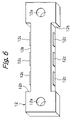
- FIG. 6 is a perspective view of a heat radiating plate forming a part of the electronic product
- FIG. 7A is a plan view of the lid member
- FIG. 7B is a side view of the lid member shown in FIG. 7A ;
- FIG. 7C is an elevation view of the lid member shown FIG. 7A ;
- FIG. 8 is a partial plan view of a lead frame used in manufacturing the electronic product
- FIG. 9 is a partial longitudinal cross-sectional view of a metal mold for molding a rectangular frame member forming a part of the electronic product
- FIG. 10 is a partial lateral cross-sectional view of the metal mold shown in FIG. 9 ;
- FIG. 11 is a perspective view of an intermediate product for the electronic product
- FIG. 12A is a perspective view of the intermediate product subjected to a first plating process
- FIG. 12B is a perspective view of the intermediate product subjected to a second plating process
- FIG. 12C is a perspective view of the intermediate product subjected to a third plating process
- FIG. 12D is a perspective view of the intermediate product subjected to a fourth plating process
- FIG. 13 is a partial plan view of a modification of the lead frame shown in FIG. 8 ;
- FIG. 14 is a lateral cross-sectional view, similar to FIG. 4 , showing a modification of the electronic product
- FIG. 15 is a lateral cross-sectional view, similar to FIG. 4 , showing another modification of the electronic product
- FIG. 16 shows a lateral cross-sectional view showing a modification of a composite lid member shown in FIG. 15 ;
- FIG. 17 shows a lateral cross-sectional view showing another modification of the composite lid member shown in FIG. 15 ;
- FIG. 18 is a lateral cross-sectional view, similar to FIG. 4 , showing a second embodiment of an electronic product according to the present invention.
- FIG. 19 is a lateral cross-sectional view, similar to FIG. 18 , showing a modification of the second embodiment of the electronic product
- FIG. 20 is a partial lateral cross-sectional view showing a modification of a lid member used in the electronic product in shown in either FIG. 18 or FIG. 19 ;
- FIG. 21 is a partial lateral cross-sectional view showing another modification of the lid member used in the electronic product in shown in either FIG. 18 or FIG. 19 ;
- FIG. 22 is a partially-cutaway perspective view, similar to FIG. 1 , showing a third embodiment of an electronic product according to the present invention
- FIG. 23 is a partially-cutaway perspective view, similar to FIG. 1 , showing a modification of the third embodiment of the electronic product according to the present invention
- FIG. 24 is a vertical cross-sectional view showing a modification of an electrically conductive layer formed on an inner wall face of a lateral side wall of a rectangular frame member which is used in the electronic product shown in FIG. 23 ;
- FIG. 25 is a vertical cross-sectional view showing another modification of the electrically conductive layer formed on the inner wall face of the lateral side wall of the rectangular frame member which is used in the electronic product shown in FIG. 23 .
- a first embodiment of an electronic product according to the present invention is generally indicated by reference 10 .
- the electronic product 10 comprises a heat radiating plate 12 made of a suitable metal material such as copper or the like, and the heat radiating plate 12 is subjected to electroplating processes, as stated in detail hereinafter.
- the heat radiating plate 12 is formed with a pair of screw holes 12 a at the ends thereof, and the screw holes 12 a are used for attaching the electronic product 10 to a suitable base frame, such as an aluminum chassis or the like, by screws (not shown), when being assembled in a piece of electronic equipment.
- the electronic product 10 comprises an electronic component 14 mounted on and adhered to the heat radiating plate 12 .
- the electronic component 14 includes a power MOSFET as a high power transistor, which is utilized in an analog amplifier or the like, and is provided with three sets of pads: first, second and third sets of pads.
- the first set of pads is provided on a top face of the electronic component 14 , and forms a drain (D) of the power MOSFET.
- the second set of pads is provided on the top face of the electronic component 14 , and forms a gate (G) of the power MOSFET.
- the third set of pads is provided on a bottom face of the electronic component 14 (not visible), and forms a source (S) of the power MOSFET.
- the electronic product 10 further comprises an enveloper 18 for encapsulating the electronic component 14 to thereby protect it from the outside.
- the enveloper 18 comprises a rectangular frame member 19 made of a suitable thermosetting resin such as epoxy resin or the like, and a lid member 20 securely attached to a top opening end of the frame member 19 .
- the lid member 20 is made of a suitable ceramic material.
- the rectangular frame member 19 is formed by a molding process, and is mechanically engaged with and attached to the heat radiating plate 12 at a bottom end thereof when being molded.
- the heat radiating plate 12 is provided with a pair of side recesses 12 b formed along the opposing longitudinal sides thereof, and three projections 12 c are integrally protruded from the inmost wall face of each side recess 12 b.
- FIG. 5 it is possible to establish the secure mechanical attachment of the frame member 14 to the heat radiating plate 12 .
- the rectangular frame member 14 is provided with a pair of shelf elements 21 and 22 , which are integrally protruded from the inner wall faces of the opposing longitudinal side walls of the frame member 14 , and which are extended between the opposing lateral side walls of the frame member 14 . Note that the functions of the shelf elements 21 and 22 are explained hereinafter.
- the lid member 20 may be securely adhered to the top opening end of the frame member 19 , using a suitable adhesive agent, to thereby close the top opening end of the frame member 19 .
- the electronic component 14 is encapsulated in the enveloper 18 , whereby it is possible to seal and protect the electronic component 14 from the outside.
- the lid member 20 is configured as shown in FIGS. 7A to 7C .
- the lid member 20 is shaped as a rectangular plate having the same rectangular profile as that of the frame member 19 , and is formed with two rectangular land portions 20 a and 20 b integrally swelled from the opposing wall faces thereof.
- the land portions 20 a are symmetrically arranged with respect to a geometrical neutral plane of the lid member 20 , and each land portion ( 20 a, 20 b ) is sized so as to be fitted into the upper opening end of the rectangular frame member 19 .
- the lid member 20 is subjected to variations in temperature, due to the symmetrical configuration of the lid member 20 , it is possible to considerably reduce warpage of the lid member 20 .
- the electronic product 10 comprises a pair of leads 23 and 24 made of a suitable metal such as copper or the like, and the respective leads 23 and 24 pass and extend through the opposing longitudinal side walls of the frame member 19 , as shown in FIGS. 1 , 2 , and 4 .
- Each of the leads 23 and 24 is mechanically held by the corresponding longitudinal side wall of the frame member 19 when the frame member 19 is molded.
- the pair of leads 23 and 24 are also subjected to electroplating processes, as stated in detail hereinafter.
- the lead frame 30 comprises an elongated metal (e.g. copper) sheet in which pairs of lead patterns 23 ′ and 24 ′ are successively formed in an openwork manner.
- a pair of lead patterns 23 ′ and 24 ′ is disposed in a molding cavity of the metal mold together with the heat radiating plate 12 .
- the pair of lead patterns 23 ′ and 24 ′ is cut off from the lead frame 30 , thereby producing the pair of leads 23 and 24 .
- each lead pattern 23 ′ is formed with a first alignment of three slots or perforations 32 and two endmost cutouts 34 , and a second alignment of three through slots or perforations 36 .
- each lead pattern 24 ′ is formed with a first alignment of three slots or perforations 38 and endmost cutouts 40 and a second alignment of three slots or perforations 42 .
- the first alignment of perforations 32 and endmost cutouts 34 in the lead pattern 23 ′ and the first alignment of perforations 38 and endmost cutouts 40 in the lead pattern 24 ′ are respectively buried in the opposing longitudinal side walls of the frame member 19 , resulting in a mechanical and secure engagement between the lead patterns 23 ′ and 24 ′ and the opposing longitudinal side walls of the frame member 19 .
- the inner lead section 23 a is electrically connected to the first set of pads 16 with bonding-wires 26 , and thus the outer lead section 23 b forms the drain terminal (D) of the power MOSFET.
- the inner lead section 24 a is electrically connected to the second set of pads 17 with bonding-wires 28 , and thus the outer lead section 24 b forms the gate terminal (G) of the power MOSFET.
- the electronic product 10 as mentioned above may be manufactured below.
- the aforesaid metal mold for molding the rectangular frame member 19 is generally indicated by reference 44 .
- the metal mold 44 comprises upper and lower mold dies 44 a and 44 b, which define a molding cavity 46 , corresponding to the profile of the rectangular frame member 19 , when being combined with each other. Namely, an upper half of the molding cavity 46 is defined by the upper mold die 44 a, and a lower half of the molding cavity 46 is defined by the lower mold die 44 b.
- the heat radiating plate 12 and the pair of lead patterns 23 ′ and 24 ′ are sandwiched by the upper and lower mold dies 44 a and 44 b such that these elements 12 , 23 ′, and 24 ′ are disposed in place in the molding cavity 46 .
- liquid epoxy resin is injected into the molding cavity 26 , and is hardened.
- the perforations 32 and 38 and cutouts 34 and 40 of the lead patterns 23 ′ and 24 ′ are filled with the injected resin, and thus the lead patterns 23 ′ and 24 ′ are mechanically and firmly engaged with the molded piece when being hardened.
- the metal mold 44 is opened, thereby obtaining an intermediate product 10 ′ as shown in FIG. 11 .
- the intermediate product 10 ′ is subjected to plating processes in accordance with a plating flow diagram shown in FIGS. 12A to 12D .
- both the heat radiating plate 12 and the lead frame 30 are plated with nickel (Ni), as represented by hatching in FIG. 12A .
- Ni nickel
- areas of these elements 12 and 30 covered by the resin material of the rectangular frame member 19 , cannot be subjected to the nickel-plating.
- the nickel-plating of the heat radiating plate 12 are further plated with silver (Ag), using an electroplating method, as represented by hatching in FIG. 12B .
- the heat radiating plate 12 is immersed together with the lead frame 30 in a solution containing Ag ions, and a negative voltage is applied to the heat radiating plate 12 , whereby the nickel-plating of the heat radiating plate 12 is further subjected to the silver plating.
- the nickel-plating surfaces of the lead frame 30 are further plated with gold, using an electroplating method, as represented by hatching in FIG. 12C .
- the lead frame 30 is immersed together with the heat radiating plate 12 in a solution containing Au ions, and a negative voltage is applied to the lead frame 30 , whereby the nickel-plating of the lead frame 30 is further subjected to the gold-plating.
- the outer portions of the heat radiating plate 12 which are outside the rectangular frame member 19 , are further plated with gold, using an electroplating method, as represented by hatching in FIG. 12D .
- the inner portion of the heat radiating plate 12 which is inside the rectangular frame member 19 , is masked with a photo-resist or the like, and the heat radiating plate 12 is immersed together with the lead frame 30 in a solution containing Au ions, and a negative voltage is applied to the heat radiating plate 12 , whereby only the silver-plating of the outer portions of the heat radiating plate 12 is further subjected to the gold-plating.
- the electronic component 14 is mounted on and adhered to the silver-plating surface of the heat radiating plate 12 , using a suitable electrically conductive bonding agent. Accordingly, as already stated, the third set of pads (not visible), provided on the bottom face of the electronic component 14 , are electrically connected to the heat radiating plate 12 , and thus the heat radiating plate 12 serves as the source terminal (S) of the power MOSFET.
- a wire-bonding process is performed to establish the electrical connections between the first set of pads 16 and the inner lead section 23 a of the lead pattern 23 ′ with the bonding-wires 26 , and between the second set pads 17 and the inner lead section 24 a of the lead pattern 24 ′ with the bonding-wires 28 .
- the respective inner lead sections 23 a and 24 a lie on the shelf elements 21 and 22 , to thereby prevent deformation of the inner lead sections 21 and 22 .
- the intermediate product 10 ′ is removed from the lead frame 30 by cutting off the lead patterns 23 ′ and 24 ′ therefrom, and then the top opening end of the frame member 19 is closed by the lid member 20 , thereby encapsulating the electronic component 14 in the enveloper 18 , resulting in a completion of the manufacture of the electronic product 10 in which the electronic component 14 is sealed and protected in the enveloper 18 from the outside.
- the molding process contributes to a flattening of the heat radiating plate 12 .
- the heat radiating plate 12 is frequently produced from a copper sheet, using a punching machine.
- the heat radiating plate 12 has a residual strain or stress, which is inevitably brought about when being punched, and thus may be warped due to the residual strain or stress.
- it is possible to flatten the warped heat radiating plate 12 during the molding process because the warped heat radiating plate 12 is clamped by the upper and lower mold dies 44 a and 44 b while the metal mold 44 is closed, as is apparent from FIGS. 9 and 10 .
- the heat radiating plate 12 is necessarily clamped by the upper and lower mold dies 44 a and 44 b, resulting in achievement of the flattening of the warped heat radiating plate 12 .
- the heat radiating plate 12 is prepared as a part which is independent from the lead frame 30 , and since the heat radiating plate 12 and the lead frame 30 are electrically isolated from each other, it is possible to individually and separately electroplate the heat radiating plate 12 and the lead frame 30 without masking either of the heat radiating plate 12 or the lead frame 30 .
- FIG. 12B while the heat radiating plate 12 is subjected to the silver-plating, it is unnecessary to mask the lead frame 30 .
- the electroplating processes FIGS. 12A to 12D ) can be easily performed at a low cost.
- the heat radiating plate 12 is independent from the lead frame 30 , the heat radiating plate 12 can be made thicker than the lead frame 30 , and thus it is possible to facilitate the radiation of heat from the heat radiating plate 12 .
- the electronic component 10 itself according to the present invention also features various advantages.
- the electronic component 10 since the electronic component 14 , the inner lead sections 23 a and 24 a, and the bonding-wires 26 and 28 are arranged in the interior space of the enveloper 18 , i.e. since these elements ( 14 , 23 a, 24 a, 26 , 28 ) are not directly covered with and sealed in a molded resin, the electronic component 10 has no relation with problems accompanying production of parasitic capacitance, resulting in an improvement in high frequency characteristics thereof.
- the enveloper 18 cannot be subjected to a thermal influence from the heated electronic component 14 , because the enveloper 18 is not in direct contact with the electronic component 14 , resulting in improvement and preservation of an operational reliability of the electronic product 10 during a high-power-output operation.
- the outer lead sections 23 b and 24 b exhibit a flexibility based on the reduction of the rigidity of the outer sections 23 b and 24 b.
- the excessive external force may be absorbed by the deformation of the outer lead sections 23 b and 24 b, resulting in the protection of the lead sections 23 b and 24 b from the damage.
- the electronic product 10 entirely exhibits a superior corrosive resistance, because the outer portions of the heat radiating plate 12 , which are outside the frame member 19 , are surfaced with the gold-plating, and because the outer lead sections 23 b and 24 b of the leads 23 and 24 are surfaced with the gold-plating.
- the gold-plating of the inner and outer lead sections ( 23 a; 23 b and 24 a; 24 b ) of the leads 23 and 24 it is possible to improve anti-migration characteristics on the leads 23 and 24 , resulting in promotion of operational reliability of the electronic product 10 .
- the inner area of the heat radiating plate 12 encompassed by the frame member 19 , is surfaced not with the gold-plating but the silver-plating, it is possible to reduce cost required for the plating processes.
- the four perforations 36 ′ included in the second alignment are alternately arranged with respect to the three perforations 32 and endmost cutouts 34 included in the first alignment.
- each of the two endmost perforations 36 ′ in the first alignment is opposed to a space area between the corresponding endmost cutout 34 and the adjacent perforations 32
- each of the two middle slots 36 ′, intervened between the two endmost perforations 36 ′ is opposed to a space area between the two corresponding adjacent perforations 32 in the second alignment.
- the same is true for a relationship between the second alignment of four perforations 42 ′ and the first alignment of three perforations 38 and two endmost cutouts 40 , formed in the lead pattern 24 ′.
- the modified lead frame 30 ′ When the modified lead frame 30 ′ is used for the manufacture of the electronic product 10 , it is possible to more effectively impede the penetration of the fused solder and flux into the interfaces between the resin frame member 19 and the leads 23 and 24 and the invasion of the fused solder and flux into the interior of the enveloper 18 through the aforesaid interfaces, due to the alternate arrangement of the four perforations ( 36 ′, 42 ′) in the second alignment with respect to the three perforations ( 32 , 38 ) and two endmost cutouts ( 34 , 40 ) in the first alignment.
- the lid member 20 is made of the ceramic material.
- the lid member 20 is made of a suitable metal material, such as, copper, silver or the like.
- the metal lid member 20 serves as an electromagnetic shield due to an electrical conductivity thereof, whereby it is possible to suppress an emission of high frequency noises from the electronic product 10 .
- the lid member 20 is made of a composite material composed of a suitable thermosetting resin, such as epoxy or the like, and suitable filler represented by a plurality of small open-triangles “ ⁇ ” in FIG. 15 .
- the filler may comprise a suitable non-conductive material, such as wood chips or pieces, ceramic chips or pieces or the like.
- the filler should comprise a suitable conductive material, such as metal chips or pieces, carbon powder or the like.
- the lid member 20 serves as an electromagnetic shield for suppressing the emission of high frequency noises from the electronic product 10 .
- FIG. 16 shows a modification of the lid member 20 , a part of which exhibits an electrical conductivity.
- the modified lid member 20 is constituted as a composite lid member comprising a metal sheet element 21 a made of a suitable metal material, such as copper, silver or the like, which is enveloped as a core body in a resin plate element 21 b made of a suitable material, such as epoxy or the like.
- This composite lid member 20 also serves as the electromagnetic shield for suppressing the emission of high frequency noises from the electronic product 10 .
- FIG. 18 similar to FIG. 4 , shows a second embodiment of an electronic product according to the present invention.
- the elements similar to those of FIG. 4 are indicated by the same references.
- the electronic product is substantially identical to the electronic product 10 except that a lid member 50 is substituted for the lid member 20 .
- the lid member 50 comprises a rectangular ceramic plate element 52 having the same profile as the lid member 20 ( FIG. 7A ), and an electrically conductive layer 54 applied to a surface of the ceramic plate element 52 , and is adhered to the top opening end of the frame member 19 with a suitable adhesive agent.
- the electrically conductive layer 54 may be formed by attaching or adhering a suitable metal sheet, made of copper, silver or the like, to the surface of the ceramic plate element 52 . Also, it is possible to perform the formation of the conductive layer 54 by a deposit of metal layer based on a sputtering process. Further, the conductive layer 54 may be formed by coating the surface of the ceramic plate element 52 with electrically conductive paste.
- the electronic product 48 is suited to the case where a high frequency signal is processed in the electronic component 14 .
- the electronic product 10 may be modified as shown in FIG. 19 .
- a resin plate element 52 ′ made of a suitable thermosetting resin material, is substituted for the ceramic plate element 52 of the lid member 50 .
- the resin plate element 52 ′ may be replaced with a composite plate element which is made of a non-conductive composite material as explained with reference to FIG. 15 .
- the composite plate element is composed of a suitable thermosetting resin, such as epoxy or the like, and a suitable non-conductive filler, such as wood chips or pieces, ceramic chips or pieces or the like.
- the lid member 50 When the lid member 50 is subjected to variation in temperature, it is possible to absorb the thermal expansion difference between the plate element ( 52 , 52 ′) and the conductive layer 54 by the regular-arrangement of the thick and thin portions 56 and 58 , resulting in mitigation of the thermal expansion difference between the plate element ( 52 , 52 ′) and the conductive layer 54 a.
- an upper end of the conductive element 62 is exposed.
- the lid member ( 20 , 50 ) exhibiting the electrical conductivity
- the lid member ( 20 , 50 ) is grounded to the heat radiating plate 12 , resulting in the prevention of the production of the parasitic capacitance.
- the electrical connection of the lid member ( 20 , 50 ) to the upper end face of the conductive element 62 can be established by adhering the lid member ( 20 , 50 ) to the upper opening end of the frame member 19 , using an electrically conductive adhesive agent.
- the conductive element 62 is embedded in only one of the opposing lateral side walls thereof, it is possible to embed an electrically conductive element in the other lateral side wall. Also, an electrically conductive element may be embedded in at least one of the opposing longitudinal side walls of the frame member 19 without being in contact with the corresponding lead ( 23 , 24 ).
- FIG. 23 shows a modification of the third embodiment shown in FIG. 22 .
- the elements similar to those of FIG. 1 are indicated by the same references.
- an electrically conductive layer 64 is applied to one inner wall face of the opposing lateral side walls of the frame member 19 .
- the electrically conductive layer 64 may be formed by attaching or adhering a suitable metal sheet, made of copper, silver or the like, to the inner surface of the lateral side wall of the frame member 19 with a suitable adhesive agent. Also, the conductive layer 64 may be formed by coating the inner surface of the lateral side wall of the frame member 19 with electrically conductive paste.
- the conductive layer 64 is in electrical contact with the heat radiating plate 12 , and is electrically connected to the lid member ( 20 , 50 ), exhibiting electrical conductivity, by adhering the lid member ( 20 , 50 ) to the upper opening end to the frame member 19 with a suitable electrically conductive adhesive agent.
- the lid member ( 20 , 50 ) is grounded to the heat radiating plate 12 , resulting in the prevention of the production of the parasitic capacitance.
- the conductive layer 64 a When the conductive layer 64 a is subjected to variation in temperature, it is possible to absorb the thermal expansion difference between the lateral side wall of the frame member 19 and the conductive layer 64 a by the regular arrangement of the thick and thin portions 66 and 88 , resulting in mitigation of the thermal expansion difference between the lateral side wall of the frame member 19 and the conductive layer 64 a.
- FIG. 25 shows another modification of the conductive layer 64 illustrated in FIG. 24 .
- the conductive layer 64 is replaced with an electrically conductive layer 64 b which is formed with a plurality of regular openings 70 .
- the conductive layer 64 b is subjected to variation in temperature, it is possible to absorb the thermal expansion difference between the lateral side wall of the frame member 19 and the conductive layer 64 b by the regular arrangement of the openings 70 , resulting in mitigation of the thermal expansion difference between the lateral side wall of the frame member 19 and the conductive layer 64 b.
Landscapes
- Engineering & Computer Science (AREA)
- Physics & Mathematics (AREA)
- Microelectronics & Electronic Packaging (AREA)
- Power Engineering (AREA)
- Condensed Matter Physics & Semiconductors (AREA)
- General Physics & Mathematics (AREA)
- Computer Hardware Design (AREA)
- Toxicology (AREA)
- Electromagnetism (AREA)
- Health & Medical Sciences (AREA)
- Manufacturing & Machinery (AREA)
- Thermal Sciences (AREA)
- Cooling Or The Like Of Semiconductors Or Solid State Devices (AREA)
- Structures Or Materials For Encapsulating Or Coating Semiconductor Devices Or Solid State Devices (AREA)
Applications Claiming Priority (2)
| Application Number | Priority Date | Filing Date | Title |
|---|---|---|---|
| JP2002052295A JP2003258141A (ja) | 2002-02-27 | 2002-02-27 | 電子部品及びその製造方法 |
| JP2002-052295 | 2002-02-27 |
Publications (2)
| Publication Number | Publication Date |
|---|---|
| US20030161109A1 US20030161109A1 (en) | 2003-08-28 |
| US7002803B2 true US7002803B2 (en) | 2006-02-21 |
Family
ID=27678532
Family Applications (1)
| Application Number | Title | Priority Date | Filing Date |
|---|---|---|---|
| US10/374,602 Expired - Fee Related US7002803B2 (en) | 2002-02-27 | 2003-02-25 | Electronic product with heat radiating plate |
Country Status (6)
| Country | Link |
|---|---|
| US (1) | US7002803B2 (de) |
| EP (1) | EP1341228A3 (de) |
| JP (1) | JP2003258141A (de) |
| KR (1) | KR20030071570A (de) |
| CN (1) | CN1226783C (de) |
| TW (1) | TW594956B (de) |
Cited By (2)
| Publication number | Priority date | Publication date | Assignee | Title |
|---|---|---|---|---|
| US20060145317A1 (en) * | 2004-12-31 | 2006-07-06 | Brennan John M | Leadframe designs for plastic cavity transistor packages |
| US20140226283A1 (en) * | 2013-02-13 | 2014-08-14 | Gerald Ho Kim | Isolation Of Thermal Ground For Multiple Heat-Generating Devices On A Substrate |
Families Citing this family (21)
| Publication number | Priority date | Publication date | Assignee | Title |
|---|---|---|---|---|
| JP4779614B2 (ja) * | 2005-12-08 | 2011-09-28 | ヤマハ株式会社 | 半導体装置 |
| US7518880B1 (en) * | 2006-02-08 | 2009-04-14 | Bi-Link | Shielding arrangement for electronic device |
| US20070230185A1 (en) * | 2006-03-31 | 2007-10-04 | Shuy Geoffrey W | Heat exchange enhancement |
| US8183680B2 (en) * | 2006-05-16 | 2012-05-22 | Broadcom Corporation | No-lead IC packages having integrated heat spreader for electromagnetic interference (EMI) shielding and thermal enhancement |
| US8450842B2 (en) * | 2007-03-20 | 2013-05-28 | Kyocera Corporation | Structure and electronics device using the structure |
| FR2939562B1 (fr) * | 2008-12-10 | 2011-01-21 | Astrium Sas | Circuit integre hyperfrequence encapsule dans un boitier. |
| JP2011096753A (ja) * | 2009-10-28 | 2011-05-12 | Kyocera Corp | 電子部品収納用パッケージおよびこれを用いた電子装置 |
| JP5293579B2 (ja) * | 2009-12-07 | 2013-09-18 | トヨタ自動車株式会社 | 電子部品用パッケージ、電子部品装置、及び電子部品用パッケージの製造方法 |
| CA2704683A1 (en) * | 2010-05-28 | 2010-08-12 | Ibm Canada Limited - Ibm Canada Limitee | Grounded lid for micro-electronic assemblies |
| JP5948693B2 (ja) * | 2012-02-24 | 2016-07-06 | 住友電工デバイス・イノベーション株式会社 | パッケージ |
| JP6296687B2 (ja) | 2012-04-27 | 2018-03-20 | キヤノン株式会社 | 電子部品、電子モジュールおよびこれらの製造方法。 |
| JP5885690B2 (ja) | 2012-04-27 | 2016-03-15 | キヤノン株式会社 | 電子部品および電子機器 |
| JP2013243340A (ja) | 2012-04-27 | 2013-12-05 | Canon Inc | 電子部品、実装部材、電子機器およびこれらの製造方法 |
| US20160071777A1 (en) * | 2013-03-28 | 2016-03-10 | Panasonic Intellectual Property Management Co., Ltd. | Semiconductor package and semiconductor device |
| JP6027569B2 (ja) * | 2014-03-26 | 2016-11-16 | エムテックスマツムラ株式会社 | 中空パッケージの製造方法および中空パッケージ |
| JP6554699B2 (ja) * | 2015-09-25 | 2019-08-07 | エムテックスマツムラ株式会社 | 中空パッケージの製造方法及び中空パッケージ |
| JP6620725B2 (ja) * | 2016-11-14 | 2019-12-18 | 株式会社オートネットワーク技術研究所 | 電気接続箱 |
| US10418291B2 (en) | 2017-09-29 | 2019-09-17 | Intel Corporation | Induced warpage of a thermal conductor |
| US10999957B2 (en) * | 2018-02-12 | 2021-05-04 | Samsung Electro-Mechanics Co., Ltd. | Communication module and mounting structure thereof |
| WO2022107697A1 (ja) * | 2020-11-17 | 2022-05-27 | 三菱電機株式会社 | パワー半導体モジュール及びその製造方法並びに電力変換装置 |
| TWI779811B (zh) * | 2021-09-01 | 2022-10-01 | 豪傑長宏科技有限公司 | 用於半導體晶片封裝的複合式封閉型金屬蓋板 |
Citations (18)
| Publication number | Priority date | Publication date | Assignee | Title |
|---|---|---|---|---|
| US3767839A (en) | 1971-06-04 | 1973-10-23 | Wells Plastics Of California I | Plastic micro-electronic packages |
| JPS50133860A (de) | 1974-04-09 | 1975-10-23 | ||
| US4139859A (en) | 1975-06-30 | 1979-02-13 | Burroughs Corporation | Semiconductor device package |
| US4458291A (en) * | 1981-07-22 | 1984-07-03 | Fujitsu Limited | Package for enclosing semiconductor elements |
| JPS607741A (ja) | 1983-06-27 | 1985-01-16 | Nec Corp | 混成集積回路装置 |
| US4876588A (en) * | 1987-09-16 | 1989-10-24 | Nec Corporation | Semiconductor device having ceramic package incorporated with a heat-radiator |
| US5012386A (en) * | 1989-10-27 | 1991-04-30 | Motorola, Inc. | High performance overmolded electronic package |
| US5041902A (en) * | 1989-12-14 | 1991-08-20 | Motorola, Inc. | Molded electronic package with compression structures |
| US5103292A (en) | 1989-11-29 | 1992-04-07 | Olin Corporation | Metal pin grid array package |
| US5315153A (en) | 1989-09-29 | 1994-05-24 | Toyo Aluminium Kabushiki Kaisha | Packages for semiconductor integrated circuit |
| EP0658935A2 (de) | 1993-12-16 | 1995-06-21 | Seiko Epson Corporation | Harzvergossenes Halbleiterbauteil und dessen Herstellungsverfahren |
| US5657203A (en) * | 1991-05-31 | 1997-08-12 | Nippondenso Co., Ltd. | Electronic device having a plurality of circuit boards arranged therein |
| US5801435A (en) * | 1995-02-27 | 1998-09-01 | Seiko Epson Corporation | Resin sealing type semiconductor device and method of making the same |
| US5814883A (en) | 1995-10-04 | 1998-09-29 | Mitsubishi Denki Kabushiki Kaisha | Packaged semiconductor chip |
| US5869883A (en) | 1997-09-26 | 1999-02-09 | Stanley Wang, President Pantronix Corp. | Packaging of semiconductor circuit in pre-molded plastic package |
| JPH11176966A (ja) | 1997-12-10 | 1999-07-02 | Hitachi Ltd | 半導体素子収納パッケージ |
| JP2001094006A (ja) | 1999-09-22 | 2001-04-06 | Hitachi Cable Ltd | 半導体素子搭載用基板及び半導体装置 |
| EP1187197A2 (de) | 2000-08-31 | 2002-03-13 | Nec Corporation | Gehäuse für ein Halbleiterchip mit einer thermisch leitenden Platte und Harzwänden |
Family Cites Families (4)
| Publication number | Priority date | Publication date | Assignee | Title |
|---|---|---|---|---|
| JPH11233696A (ja) * | 1998-02-17 | 1999-08-27 | Mitsubishi Electric Corp | パワー半導体モジュール及びパワー半導体モジュールと冷却装置の接合体 |
| US6362964B1 (en) * | 1999-11-17 | 2002-03-26 | International Rectifier Corp. | Flexible power assembly |
| JP3433732B2 (ja) * | 2000-11-22 | 2003-08-04 | 住友電気工業株式会社 | 光半導体気密封止容器及び光半導体モジュール並びに光ファイバー増幅器 |
| KR20030046795A (ko) * | 2001-12-06 | 2003-06-18 | 삼성전자주식회사 | 안내 벽이 형성된 방열판을 갖는 고전력 패키지 |
-
2002
- 2002-02-27 JP JP2002052295A patent/JP2003258141A/ja active Pending
-
2003
- 2003-02-25 US US10/374,602 patent/US7002803B2/en not_active Expired - Fee Related
- 2003-02-26 TW TW092104134A patent/TW594956B/zh not_active IP Right Cessation
- 2003-02-27 KR KR10-2003-0012481A patent/KR20030071570A/ko not_active Application Discontinuation
- 2003-02-27 EP EP03004467A patent/EP1341228A3/de not_active Withdrawn
- 2003-02-27 CN CNB031064744A patent/CN1226783C/zh not_active Expired - Fee Related
Patent Citations (20)
| Publication number | Priority date | Publication date | Assignee | Title |
|---|---|---|---|---|
| US3767839A (en) | 1971-06-04 | 1973-10-23 | Wells Plastics Of California I | Plastic micro-electronic packages |
| JPS50133860A (de) | 1974-04-09 | 1975-10-23 | ||
| US4139859A (en) | 1975-06-30 | 1979-02-13 | Burroughs Corporation | Semiconductor device package |
| US4458291A (en) * | 1981-07-22 | 1984-07-03 | Fujitsu Limited | Package for enclosing semiconductor elements |
| JPS607741A (ja) | 1983-06-27 | 1985-01-16 | Nec Corp | 混成集積回路装置 |
| US4876588A (en) * | 1987-09-16 | 1989-10-24 | Nec Corporation | Semiconductor device having ceramic package incorporated with a heat-radiator |
| US5315153A (en) | 1989-09-29 | 1994-05-24 | Toyo Aluminium Kabushiki Kaisha | Packages for semiconductor integrated circuit |
| US5012386A (en) * | 1989-10-27 | 1991-04-30 | Motorola, Inc. | High performance overmolded electronic package |
| US5103292A (en) | 1989-11-29 | 1992-04-07 | Olin Corporation | Metal pin grid array package |
| US5041902A (en) * | 1989-12-14 | 1991-08-20 | Motorola, Inc. | Molded electronic package with compression structures |
| US5657203A (en) * | 1991-05-31 | 1997-08-12 | Nippondenso Co., Ltd. | Electronic device having a plurality of circuit boards arranged therein |
| EP0658935A2 (de) | 1993-12-16 | 1995-06-21 | Seiko Epson Corporation | Harzvergossenes Halbleiterbauteil und dessen Herstellungsverfahren |
| US5801435A (en) * | 1995-02-27 | 1998-09-01 | Seiko Epson Corporation | Resin sealing type semiconductor device and method of making the same |
| US5814883A (en) | 1995-10-04 | 1998-09-29 | Mitsubishi Denki Kabushiki Kaisha | Packaged semiconductor chip |
| US5869883A (en) | 1997-09-26 | 1999-02-09 | Stanley Wang, President Pantronix Corp. | Packaging of semiconductor circuit in pre-molded plastic package |
| JPH11176966A (ja) | 1997-12-10 | 1999-07-02 | Hitachi Ltd | 半導体素子収納パッケージ |
| EP0928026A1 (de) | 1997-12-10 | 1999-07-07 | Hitachi, Ltd. | Gegossenes Kunststoffgehäuse für ein Halbleiterbauelement |
| JP2001094006A (ja) | 1999-09-22 | 2001-04-06 | Hitachi Cable Ltd | 半導体素子搭載用基板及び半導体装置 |
| EP1187197A2 (de) | 2000-08-31 | 2002-03-13 | Nec Corporation | Gehäuse für ein Halbleiterchip mit einer thermisch leitenden Platte und Harzwänden |
| JP2002076158A (ja) | 2000-08-31 | 2002-03-15 | Nec Corp | 半導体装置及びその製造方法 |
Cited By (3)
| Publication number | Priority date | Publication date | Assignee | Title |
|---|---|---|---|---|
| US20060145317A1 (en) * | 2004-12-31 | 2006-07-06 | Brennan John M | Leadframe designs for plastic cavity transistor packages |
| US20140226283A1 (en) * | 2013-02-13 | 2014-08-14 | Gerald Ho Kim | Isolation Of Thermal Ground For Multiple Heat-Generating Devices On A Substrate |
| US9258878B2 (en) * | 2013-02-13 | 2016-02-09 | Gerald Ho Kim | Isolation of thermal ground for multiple heat-generating devices on a substrate |
Also Published As
| Publication number | Publication date |
|---|---|
| CN1226783C (zh) | 2005-11-09 |
| JP2003258141A (ja) | 2003-09-12 |
| CN1441484A (zh) | 2003-09-10 |
| EP1341228A2 (de) | 2003-09-03 |
| US20030161109A1 (en) | 2003-08-28 |
| KR20030071570A (ko) | 2003-09-03 |
| TW200303608A (en) | 2003-09-01 |
| TW594956B (en) | 2004-06-21 |
| EP1341228A3 (de) | 2004-04-07 |
Similar Documents
| Publication | Publication Date | Title |
|---|---|---|
| US7002803B2 (en) | Electronic product with heat radiating plate | |
| US6965157B1 (en) | Semiconductor package with exposed die pad and body-locking leadframe | |
| US6002165A (en) | Multilayered lead frame for semiconductor packages | |
| EP3226292B1 (de) | Leiterrahmen, halbleiterbauelement, verfahren zur herstellung eines leiterrahmens und verfahren zur herstellung eines halbleiterbauelements | |
| US5703398A (en) | Semiconductor integrated circuit device and method of producing the semiconductor integrated circuit device | |
| US7495323B2 (en) | Semiconductor package structure having multiple heat dissipation paths and method of manufacture | |
| US7566955B2 (en) | High-frequency chip packages | |
| CN109935574B (zh) | 半导体模块和用于生产半导体模块的方法 | |
| US5672908A (en) | Thin semiconductor integrated circuit device assembly | |
| US6983537B2 (en) | Method of making a plastic package with an air cavity | |
| US9142492B2 (en) | Leadframe package with integrated partial waveguide interface | |
| JP3533159B2 (ja) | 半導体装置及びその製造方法 | |
| US5229918A (en) | Metal heat sink baseplate for a semiconductor device | |
| US20220108931A1 (en) | Semiconductor package, semiconductor device, and method for manufacturing semiconductor device | |
| KR102396096B1 (ko) | 고주파 반도체 소자 패키지 및 그 제조 방법 | |
| US9230831B2 (en) | Semiconductor device and a manufacturing method thereof | |
| JP2740977B2 (ja) | 半導体装置 | |
| JPH11260968A (ja) | 複合半導体装置 | |
| US6312976B1 (en) | Method for manufacturing leadless semiconductor chip package | |
| JP3274452B2 (ja) | 高周波回路用パッケージ及びその製造方法 | |
| JPH0278298A (ja) | 電子装置 | |
| JPH06326227A (ja) | 多層リードフレームの製造方法及び構造 | |
| KR19980033656A (ko) | 반도체 패키지 및 그 제조방법 | |
| CN117012651A (zh) | 用于制造半导体设备的方法和对应的半导体设备 | |
| JPH06291243A (ja) | 半導体装置用パッケージ及びその製造方法並びに半導体装置 |
Legal Events
| Date | Code | Title | Description |
|---|---|---|---|
| AS | Assignment |
Owner name: NEC COMPOUND SEMICONDUCTOR DEVICES, LTD., JAPAN Free format text: ASSIGNMENT OF ASSIGNORS INTEREST;ASSIGNORS:KURIHARA, TOSHIMICHI;UEDA, TAKASHI;REEL/FRAME:013824/0627 Effective date: 20030212 |
|
| FEPP | Fee payment procedure |
Free format text: PAYOR NUMBER ASSIGNED (ORIGINAL EVENT CODE: ASPN); ENTITY STATUS OF PATENT OWNER: LARGE ENTITY |
|
| AS | Assignment |
Owner name: NEC ELECTRONICS CORPORATION, JAPAN Free format text: ASSIGNMENT OF ASSIGNORS INTEREST;ASSIGNOR:NEC COMPOUND SEMICONDUCTOR DEVICES, LTD.;REEL/FRAME:017730/0697 Effective date: 20060315 |
|
| FPAY | Fee payment |
Year of fee payment: 4 |
|
| AS | Assignment |
Owner name: RENESAS ELECTRONICS CORPORATION, JAPAN Free format text: CHANGE OF NAME;ASSIGNOR:NEC ELECTRONICS CORPORATION;REEL/FRAME:025525/0154 Effective date: 20100401 |
|
| FPAY | Fee payment |
Year of fee payment: 8 |
|
| FEPP | Fee payment procedure |
Free format text: MAINTENANCE FEE REMINDER MAILED (ORIGINAL EVENT CODE: REM.) |
|
| LAPS | Lapse for failure to pay maintenance fees |
Free format text: PATENT EXPIRED FOR FAILURE TO PAY MAINTENANCE FEES (ORIGINAL EVENT CODE: EXP.) |
|
| STCH | Information on status: patent discontinuation |
Free format text: PATENT EXPIRED DUE TO NONPAYMENT OF MAINTENANCE FEES UNDER 37 CFR 1.362 |
|
| FP | Lapsed due to failure to pay maintenance fee |
Effective date: 20180221 |