US6483136B1 - Semiconductor integrated circuit and method of fabricating the same - Google Patents
Semiconductor integrated circuit and method of fabricating the same Download PDFInfo
- Publication number
- US6483136B1 US6483136B1 US09/446,302 US44630200A US6483136B1 US 6483136 B1 US6483136 B1 US 6483136B1 US 44630200 A US44630200 A US 44630200A US 6483136 B1 US6483136 B1 US 6483136B1
- Authority
- US
- United States
- Prior art keywords
- bit lines
- integrated circuit
- memory cell
- semiconductor integrated
- circuit device
- Prior art date
- Legal status (The legal status is an assumption and is not a legal conclusion. Google has not performed a legal analysis and makes no representation as to the accuracy of the status listed.)
- Expired - Lifetime
Links
- 239000004065 semiconductor Substances 0.000 title claims abstract description 143
- 238000004519 manufacturing process Methods 0.000 title claims description 38
- 239000000758 substrate Substances 0.000 claims abstract description 90
- 229910052751 metal Inorganic materials 0.000 claims abstract description 18
- 239000002184 metal Substances 0.000 claims abstract description 18
- 230000005669 field effect Effects 0.000 claims abstract description 14
- 239000012212 insulator Substances 0.000 claims abstract description 14
- 238000000034 method Methods 0.000 claims description 48
- 238000005530 etching Methods 0.000 claims description 42
- 238000009825 accumulation Methods 0.000 claims description 35
- 229910021420 polycrystalline silicon Inorganic materials 0.000 claims description 30
- 238000002955 isolation Methods 0.000 claims description 27
- 238000000206 photolithography Methods 0.000 claims description 24
- 238000000926 separation method Methods 0.000 claims description 19
- 239000012535 impurity Substances 0.000 claims description 16
- 238000000059 patterning Methods 0.000 claims description 9
- 230000003071 parasitic effect Effects 0.000 claims description 5
- 238000013500 data storage Methods 0.000 claims description 4
- 239000004020 conductor Substances 0.000 claims 2
- HQVNEWCFYHHQES-UHFFFAOYSA-N silicon nitride Chemical compound N12[Si]34N5[Si]62N3[Si]51N64 HQVNEWCFYHHQES-UHFFFAOYSA-N 0.000 description 60
- VYPSYNLAJGMNEJ-UHFFFAOYSA-N Silicium dioxide Chemical compound O=[Si]=O VYPSYNLAJGMNEJ-UHFFFAOYSA-N 0.000 description 58
- 229910052814 silicon oxide Inorganic materials 0.000 description 58
- 229910052581 Si3N4 Inorganic materials 0.000 description 43
- 239000010410 layer Substances 0.000 description 26
- 238000010586 diagram Methods 0.000 description 24
- 229920005591 polysilicon Polymers 0.000 description 22
- 229920002120 photoresistant polymer Polymers 0.000 description 20
- 238000005229 chemical vapour deposition Methods 0.000 description 17
- 229910052698 phosphorus Inorganic materials 0.000 description 13
- 239000011574 phosphorus Substances 0.000 description 13
- OAICVXFJPJFONN-UHFFFAOYSA-N Phosphorus Chemical compound [P] OAICVXFJPJFONN-UHFFFAOYSA-N 0.000 description 12
- 125000006850 spacer group Chemical group 0.000 description 9
- 238000000151 deposition Methods 0.000 description 8
- ATJFFYVFTNAWJD-UHFFFAOYSA-N Tin Chemical compound [Sn] ATJFFYVFTNAWJD-UHFFFAOYSA-N 0.000 description 6
- 239000003990 capacitor Substances 0.000 description 5
- 238000005468 ion implantation Methods 0.000 description 5
- 230000008569 process Effects 0.000 description 5
- 230000001133 acceleration Effects 0.000 description 4
- 230000015572 biosynthetic process Effects 0.000 description 4
- 238000005498 polishing Methods 0.000 description 3
- 238000004544 sputter deposition Methods 0.000 description 3
- ZOXJGFHDIHLPTG-UHFFFAOYSA-N Boron Chemical compound [B] ZOXJGFHDIHLPTG-UHFFFAOYSA-N 0.000 description 2
- NBIIXXVUZAFLBC-UHFFFAOYSA-N Phosphoric acid Chemical compound OP(O)(O)=O NBIIXXVUZAFLBC-UHFFFAOYSA-N 0.000 description 2
- 230000004913 activation Effects 0.000 description 2
- 229910052796 boron Inorganic materials 0.000 description 2
- 230000008030 elimination Effects 0.000 description 2
- 238000003379 elimination reaction Methods 0.000 description 2
- 238000009413 insulation Methods 0.000 description 2
- 239000011229 interlayer Substances 0.000 description 2
- 238000003475 lamination Methods 0.000 description 2
- 239000011159 matrix material Substances 0.000 description 2
- 230000003647 oxidation Effects 0.000 description 2
- 238000007254 oxidation reaction Methods 0.000 description 2
- BPUBBGLMJRNUCC-UHFFFAOYSA-N oxygen(2-);tantalum(5+) Chemical compound [O-2].[O-2].[O-2].[O-2].[O-2].[Ta+5].[Ta+5] BPUBBGLMJRNUCC-UHFFFAOYSA-N 0.000 description 2
- 230000002093 peripheral effect Effects 0.000 description 2
- 230000002265 prevention Effects 0.000 description 2
- 230000000717 retained effect Effects 0.000 description 2
- 239000000126 substance Substances 0.000 description 2
- 230000001629 suppression Effects 0.000 description 2
- 238000001039 wet etching Methods 0.000 description 2
- 229910015900 BF3 Inorganic materials 0.000 description 1
- 241000293849 Cordylanthus Species 0.000 description 1
- XUIMIQQOPSSXEZ-UHFFFAOYSA-N Silicon Chemical compound [Si] XUIMIQQOPSSXEZ-UHFFFAOYSA-N 0.000 description 1
- 229910000147 aluminium phosphate Inorganic materials 0.000 description 1
- 230000008901 benefit Effects 0.000 description 1
- WTEOIRVLGSZEPR-UHFFFAOYSA-N boron trifluoride Chemical compound FB(F)F WTEOIRVLGSZEPR-UHFFFAOYSA-N 0.000 description 1
- 238000004140 cleaning Methods 0.000 description 1
- 239000000470 constituent Substances 0.000 description 1
- 230000007547 defect Effects 0.000 description 1
- 238000000280 densification Methods 0.000 description 1
- 230000000694 effects Effects 0.000 description 1
- 238000005516 engineering process Methods 0.000 description 1
- 230000006872 improvement Effects 0.000 description 1
- 230000010354 integration Effects 0.000 description 1
- 239000000463 material Substances 0.000 description 1
- 238000013508 migration Methods 0.000 description 1
- 238000007517 polishing process Methods 0.000 description 1
- 230000002250 progressing effect Effects 0.000 description 1
- 230000009467 reduction Effects 0.000 description 1
- 230000003252 repetitive effect Effects 0.000 description 1
- 229910052710 silicon Inorganic materials 0.000 description 1
- 239000010703 silicon Substances 0.000 description 1
- 238000005245 sintering Methods 0.000 description 1
- 238000009751 slip forming Methods 0.000 description 1
- WFKWXMTUELFFGS-UHFFFAOYSA-N tungsten Chemical compound [W] WFKWXMTUELFFGS-UHFFFAOYSA-N 0.000 description 1
- 229910052721 tungsten Inorganic materials 0.000 description 1
- 239000010937 tungsten Substances 0.000 description 1
- 238000009279 wet oxidation reaction Methods 0.000 description 1
Images


Classifications
-
- H—ELECTRICITY
- H10—SEMICONDUCTOR DEVICES; ELECTRIC SOLID-STATE DEVICES NOT OTHERWISE PROVIDED FOR
- H10B—ELECTRONIC MEMORY DEVICES
- H10B12/00—Dynamic random access memory [DRAM] devices
- H10B12/30—DRAM devices comprising one-transistor - one-capacitor [1T-1C] memory cells
- H10B12/31—DRAM devices comprising one-transistor - one-capacitor [1T-1C] memory cells having a storage electrode stacked over the transistor
- H10B12/318—DRAM devices comprising one-transistor - one-capacitor [1T-1C] memory cells having a storage electrode stacked over the transistor the storage electrode having multiple segments
-
- H—ELECTRICITY
- H10—SEMICONDUCTOR DEVICES; ELECTRIC SOLID-STATE DEVICES NOT OTHERWISE PROVIDED FOR
- H10B—ELECTRONIC MEMORY DEVICES
- H10B12/00—Dynamic random access memory [DRAM] devices
-
- H—ELECTRICITY
- H10—SEMICONDUCTOR DEVICES; ELECTRIC SOLID-STATE DEVICES NOT OTHERWISE PROVIDED FOR
- H10B—ELECTRONIC MEMORY DEVICES
- H10B12/00—Dynamic random access memory [DRAM] devices
- H10B12/01—Manufacture or treatment
- H10B12/02—Manufacture or treatment for one transistor one-capacitor [1T-1C] memory cells
- H10B12/03—Making the capacitor or connections thereto
- H10B12/033—Making the capacitor or connections thereto the capacitor extending over the transistor
Definitions
- the present invention relates generally to semiconductor integrated circuit devices and manufacturing architectures of the same. More particularly but not exclusively, the invention relates to those technologies adaptable for use with semiconductor integrated circuit devices having dynamic random access memory (“DRAM”) modules.
- DRAM dynamic random access memory
- DRAMs are typically designed to include an array of rows and columns of memory cells as disposed in a matrix form on a principal surface of a semiconductive substrate at those cross points or “intersections” between a plurality of word lines and a plurality of bit lines, wherein each of the memory cells consists essentially of a capacitive element for accumulation of information and a metal insulator semiconductor field effect transistor (MISFET) for use in selecting a single memory cell, which is serially connected to the capacitive element.
- MISFET metal insulator semiconductor field effect transistor
- the MISFET is generally designed to consist of a gate oxide film and a gate electrode integral with a corresponding one of the word lines plus a pair of semiconductor active regions for use as a source and drain of the transistor.
- a bit line is disposed to overlie the memory cell selecting MISFET in a manner such that it is electrically connected to one of the source and drain which is commonly shared by two memory cell selection MISFETs.
- the information accumulation capacitive element is laid out at a location overlying the memory cell select MISFET and is electrically coupled to the remaining one of the source and drain.
- a DRAM device with the memory cell structure of this type has been disclosed in Published Unexamined Japanese Patent Laid-Open No. 5-291532 and other publications.
- the memory cells of the DRAM as disclosed therein are designed so that word lines are increased in width or made “fat” in active regions (the regions in each of which a word line serves as the gate electrode of a memory cell select MISFET) and reduced in width or “thinned” in the remaining regions in order to retain the required gate length when miniaturizing or “downsizing” the memory cell select MISFETs while at the same time minimizing the pitch of word lines.
- the DRAM memory cells as taught by the Japanese Application above is arranged so that the bit lines are partly fattened to extend up to those portions overlying the active regions and that a planar pattern of such active regions is designed into a gull-wing shape with part of it being bent toward the bit line side in order to achieve successful electrical conduction of more than one contact hole for use in connecting between one of the source and drain of a memory cell select MISFET and its corresponding bit line operatively associated therewith.
- the DRAM memory cells taught by the above Japanese Application is faced with a problem as to an inability to provide any excellent size/dimension accuracy when partly increasing the widths of word lines and bit lines or when employing the gullwing-shaped planar pattern of the active regions due to the fact that present available photolithography techniques suffer from difficulties in accurately achieving ultra-fine resolution of curved-line patterns and/or folded-line patterns in cases where the minimal fabricatable size becomes at or near a limit of resolution in photolithography processes as a result of further progressing in microfabrication or miniaturization of such memory cells.
- Another problem faced with the prior art DRAM device is that as a through-going hole for use in connecting between the lower-side electrode of an information accumulation capacitive element and the remaining one of the source and drain of its associated memory cell select MISFET is inherently disposed between a bit line and a bit line, partly fattening the bit lines makes it difficult to attain the intended through-hole opening margin, which leads to incapability of assuring elimination of unwanted electrical short-circuiting between the lower-side electrode within a though-hole and its associative one of the bit lines.
- a semiconductor integrated circuit device incorporating the principles of the invention is arranged to a semiconductor integrated circuit device comprising a plurality of word lines extending in a first direction on a principal surface of a semiconductive substrate, a plurality of bits lines extending in a second direction at right angles to the first direction, and an array of memory cells of a DRAM as disposed at cross points of said word lines and said bit lines, each said memory cell including a serial combination of a memory cell selecting MISFET with a gate electrode as integrally formed with a corresponding one of said word lines and a capacitive element for information accumulation, wherein said plurality of word lines are arranged to linearly extend in the first direction on the principal surface of said semiconductive substrate with an identical width, and wherein a distance between adjacent ones of said word lines is less than said width.
- the semiconductor integrated circuit device of the invention is such that the distance between the adjacent ones of said gate electrodes is set at a minimal size as determinable by a resolution limit of photolithography.
- the semiconductor integrated circuit device of the invention is such that said word lines and the gate electrode of said memory cell selecting MISFET as integrally formed with a corresponding one of said word lines are comprised of a conductive film at least partially including a metallic film therein.
- the semiconductor integrated circuit device of the invention is such that said semiconductive substrate has an active region with said memory cell selecting MISFET formed therein and being arranged to have an island-like pattern extending in the second direction on the principal surface of said semiconductive substrate while having its periphery as surrounded by an element isolation region.
- the semiconductor integrated circuit device of the invention is such that the element isolation region surrounding said active region is formed of an element separation groove having a dielectric film embedded therein as defined in the principal surface of said semiconductive substrate.
- the semiconductor integrated circuit device of the invention is such that said bit lines are formed overlying said memory cell selecting MISFET with an insulative film laid there between, wherein a contact hole for electrical connection between one of a source and drain of said memory cell selecting MISFET and a corresponding one of said bit lines is formed in self-alignment with the gate electrode of said memory cell selecting MISFET.
- the semiconductor integrated circuit device of the invention is such that said information accumulation capacitive element is formed to overlie said memory cell selecting MISFET with an insulative film laid therebetween, wherein a contact hole for electrical connection between the other of the source and drain of said memory cell selecting MISFET and one electrode of said information accumulation capacitive element is formed in self-alignment with the gate electrode of said memory cell selecting MISFET.
- the present invention also provides a semiconductor integrated circuit device comprising a plurality of word lines extending in a first direction on a principal surface of a semiconductive substrate, a plurality of bit lines extending in a second direction at right angles to the first direction, and an array of DRAM memory cells as disposed at intersections of said word lines and said bit lines, each said memory cell including a serial combination of a memory cell selecting MISFET with a gate electrode as integrally formed with a corresponding one of said word lines and a capacitive element for information accumulation, wherein said bit lines straightly extend in the second direction on the principal surface of said semiconductive substrate with an identical width and wherein a distance between adjacent ones of said bit lines is greater than said width.
- the semiconductor integrated circuit device of the invention is such that the width of each said bit lines is equal to or less than a minimal size determinable by a resolution limit of photolithography.
- the semiconductor integrated circuit device of the invention is such that said bit lines are comprised of a conductive film at least partially containing a metallic film.
- the invention further provides a semiconductor integrated circuit device comprising a plurality of word lines extending in a first direction on a principal surface of a semiconductor substrate, a plurality of bit lines extending in a second direction at right angles to the first direction, and an array of DRAM memory cells as disposed at intersections of said word lines and said bit lines, each said memory cell including a serial combination of a memory cell selecting MISFET with a gate electrode as integrally formed with a corresponding one of said word lines and a capacitive element for information accumulation, wherein an active region with said memory cell selecting MISFET formed therein is arranged to have an island-like pattern extending in the second direction on the principal surface of said semiconductive substrate while having its periphery as surrounded by an element isolation region, wherein said plurality of word lines extend along the first direction on the principal surface of said semiconductive substrate with an identical width at a distance between adjacent ones thereof, wherein certain one of said bit lines as formed overlying said element isolation region with a first insulative film laid therebetween extends in
- the semiconductor integrated circuit device of the invention is such that said first contact hole includes a polycrystalline silicon film as formed therein, wherein said polycrystalline silicon film is doped with a chosen impurity equal in conductivity type to the source and drain of said memory cell selecting MISFET.
- the semiconductor integrated circuit device of the invention is such that the corresponding one of said bit lines and said one of the source and drain of said memory cell selecting MISFET are electrically connected together via a first through-hole as formed in a second insulative film sandwiched between said bit lines and said first insulative film.
- the semiconductor integrated circuit device of the invention is such that the width of said bit lines is less than a diameter of said first through-hole.
- the semiconductor integrated circuit device of the invention is such that said first contact hole has a diameter in the first direction greater than in the second direction, where a portion of the contact hole consists essentially of a first region extending to overlie said element isolation region and a second region as formed beneath said first region to have a diameter in the first direction and diameter in the second direction being substantially equal thereto, wherein said first region is formed overlying said memory cell selecting MISFET.
- the semiconductor integrated circuit device of the invention is such that said information accumulation capacitive element is formed over said bit lines with a third insulative film laid therebetween and is electrically connected to a remaining one of the source and drain of said memory cell selecting MISFET via a second through-hole formed in said third insulative film and a second contact hole as formed in said first insulative film at a location underlying said second through-hole.
- the semiconductor integrated circuit device of the invention is such that said second contact hole includes a polycrystalline silicon film being embedded therein and doped with an impurity equal in conductivity type to the source and drain of said memory cell selecting MISFET.
- the semiconductor integrated circuit device of the invention is such that said second through-hole is disposed between neighboring ones of said bit lines and is formed in self-alignment therewith.
- a semiconductor integrated circuit device of the present invention comprises: an array of memory cells each including a serial combination of a MISFET for memory cell selection having a source and drain plus insulated gate electrode and a capacitive element for data storage having first and second electrodes with a dielectric film laid therebetween; word lines including first, second and third ones extending in a first direction on a principal surface of a semiconductive substrate and each having part used as the gate electrode of its associated memory cell selecting MISFET; and, bit lines including first and second ones as disposed adjacent to each other to extend in a second direction at right angles to the first direction on the principal surface of the semiconductive substrate, wherein the first to third word lines are substantially identical in width to one another, a distance between the first word line and the second word line neighboring thereto is substantially equal to a distance between the second word line and the third word line next thereto, the distance is less than the width, the first and second bit lines are substantially the same as each other in width, which is greater than the width of these bit lines.
- the semiconductor integrated circuit device of this invention further comprises a first conductive layer provided between the first and second word lines for connecting the first bit line to either one of the source and drain of the memory-cell selecting MISFET and a second conductive layer laid between the second and third word lines for connecting the remaining one of the source and drain of the memory-cell selecting MISFET to the first electrode of the data storage capacitive element, wherein the aforesaid one of the source and drain of the memory-cell selecting MISFET and the first conductive layer are in self-alignment with the first word line and the second word line whereas the remaining one of the source and drain of the memory-cell selecting MISFET and the second conductive layer are self-aligned with the second word line and the third word line.
- the invention further provides a method for manufacturing a semiconductor integrated circuit device comprising a plurality of word lines extending in a first direction on a principal surface of a semiconductive substrate, a plurality of bit lines extending in a second direction at right angles to the first direction, and an array of DRAM memory cells as disposed at intersections of said word lines and said bit lines, each said memory cell including a serial combination of a memory cell selecting MISFET with a gate electrode as integrally formed with a corresponding one of said word lines and a capacitive element for information accumulation, said method comprising the steps of:
- the gate electrodes are fabricated so that the distance of adjacent ones thereof is set at a minimal size determinable by a resolution limit in photolithography.
- the semiconductor integrated circuit device manufacturing method is arranged to include, after said step (c), further process steps of:
- the semiconductor integrated circuit device manufacturing method is such that the width of said bit lines is formed to be equal in dimension to or less than a minimal size determinable by a photolithography resolution limit.
- the semiconductor integrated circuit device manufacturing method is arranged to include, after said step (g), further steps of:
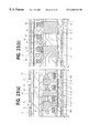
- FIG. 1 is a diagram depicting equivalent circuitry of a DRAM device in accordance with Embodiment 1 of the present invention.
- FIG. 2 is a diagram schematically showing a plan view of major part of memory array of the DRAM in accordance with the Embodiment 1 of this invention.
- FIG. 3 is a diagram showing an enlarged plan view of a portion of the FIG. 2 .
- FIG. 4 is a diagram showing a sectional view of a semiconductor substrate along both line A—A′ line and B—B′ of FIG. 3 .
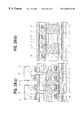
- FIGS. 5 to 7 are each a diagram illustrating, in cross-section, main part of the semiconductor substrate at a process step in the manufacture of memory cells of the DRAM of the Embodiment 1 of the invention.
- FIG. 8 is a diagram depicting a plan view of the main part of the semiconductor substrate at the step during manufacture of the DRAM memory cells of Embodiment 1 of the invention.
- FIGS. 9 and 10 are each a diagram depicting in cross-section main part of the semiconductor substrate at a step during manufacture of the DRAM memory cells of Embodiment 1 of the invention.
- FIG. 11 is a diagram showing in plan view main part of the semiconductor substrate at the step during manufacture of the DRAM memory cells of Embodiment 1 of the invention.
- FIGS. 12 to 14 are each a diagram showing in cross-section main part of the semiconductor substrate at a process step during manufacture of the DRAM memory cells of Embodiment 1 of the invention.
- FIG. 15 is a diagram showing, in plan view, main part of the semiconductor substrate at the step during manufacture of the DRAM memory cells of Embodiment 1 of the invention.
- FIGS. 16 and 17 are each a diagram showing in cross-section main part of the semiconductor substrate at a step during manufacture of the DRAM memory cells of Embodiment 1 of the invention.
- FIG. 18 is a diagram depicting, in plan view, main part of the semiconductor substrate at the step during manufacture of the DRAM memory cells of Embodiment 1 of the invention.
- FIG. 19 is a diagram showing in cross-section main part of the semiconductor substrate at a step during manufacture of the DRAM memory cells of Embodiment 1 of the invention.
- FIG. 20 is a digram showing in plan view main part of the semiconductor substrate at the step during manufacture of the DRAM memory cell of Embodiment 1 of the invention.
- FIGS. 21 to 24 are each a diagram showing in cross-section main part of the semiconductor substrate at a step during manufacture of the DRAM memory cell of Embodiment 1 of the invention.
- FIG. 25 is a diagram showing a plan view of the main part of the semiconductor substrate at the step during manufacture of the DRAM memory cell of Embodiment 1 of the invention.
- FIGS. 26 to 30 are each a diagram showing in cross-section main part of the semiconductor substrate at a step during manufacture of the DRAM memory cell of Embodiment 1 of the invention.
- FIG. 31 is a diagram showing a plan view of the main part of a semiconductor substrate at a step in the manufacture of a memory cell of a DRAM of Embodiment 2 of the invention.
- FIG. 32 is a diagram showing in cross-section main part of the semiconductor substrate at a step during manufacture of the DRAM memory cell of Embodiment 2 of the invention.
- FIG. 33 is a diagram depicting an enlarged plan view of the main part of the semiconductor substrate at a step during manufacture of the DRAM memory cell of Embodiment 2 of the invention.
- FIGS. 34 to 36 are each a diagram showing in cross-section main part of the semiconductor substrate at a step during manufacture of the DRAM memory cell of Embodiment 2 of the invention.
- FIG. 37 is a diagram showing plan view of the main part of the semiconductor substrate at a process step during manufacture of the DRAM memory cell of Embodiment 3 of the invention.
- FIGS. 38 to 42 are each a diagram showing in cross-section main part of the semiconductor substrate at a process step during manufacture of the DRAM memory cell of Embodiment 3 of the invention.
- FIG. 1 is a diagram illustrating electrical equivalent circuitry of a dynamic random access memory (DRAM) device in accordance with one embodiment of the present invention.
- the DRAM clip includes a memory array (MARY) that is configured from a plurality of memory cells (MC) organized into a matrix form at those intersections between a plurality of word lies WL (WLn- 1 , WLn, WLn+ 1 •••) and a plurality of bit lies BL.
- a single memory cell for storing therein a 1-bit information or data is comprised of a serial combination of a capacitive element C for information accumulation and a metal insulator semiconductor field effect transistor (MISFET) Qs for memory cell selection.
- MISFET metal insulator semiconductor field effect transistor
- the memory-cell selecting MISFET Qs has its source and drain, one of which is electrically connected to the information accumulation capacitive element C and the other of which is electrically coupled to a corresponding one of the bit lines BL.
- the word lines WL are connected at certain ends thereof to a word driver circuit WD whereas the bit lines BL are coupled at their selected ends to sense amplifier circuits SA operatively associated therewith.
- FIG. 2 is a diagram schematically depicting an enlarged plan view of part of the memory array integrated on the semiconductor substrate;
- FIG. 3 is an enlarged plan view of part of FIG. 2; and
- FIG. 4 shows at its left-hand portion a cross-sectional view as taken along line A—A′ of FIG. 3 and also shows at its right-hand portion a sectional view along line B—B′ of the same.
- FIG. 2 and FIG. 3 indicate only those conductive layers (expect plate electrodes) which make up the memory cells while illustration of any dielectric films between conductive layers and on-chip leads overlying the memory cells is eliminated therein.
- the memory cells of the DRAM are each formed in a p-type well 2 that is formed on the principal surface of a semiconductive substrate 1 of p-type conductivity.
- the planar size of each memory cell is, for example, 0.46 ⁇ m ⁇ 0.46 ⁇ m.
- the p-type well 2 with the memory cell formed therein is electrically separated from the p-type semiconductor substrate 1 by an n-type semiconductor region 3 that is formed beneath the well in order to eliminate the influence of noises from circuitry formed in the other regions of the semiconductor substrate 1 (such as for example an input/output circuit as part of peripheral circuitry).
- the memory-cell select MISFET Qs of a memory cell may be an n-channel type one which is formed in an active region L of the p-type well 2 .
- this active region L is designed to have an elongate island-like shape that linearly extends along the lateral direction (X direction) in the drawings, wherein its size in the X direction is 1.16 ⁇ m whereas the size in up-down direction (Y direction) is 0.24 ⁇ m.
- any hard-to-resolve ultrafine pattern will no longer take place even when downsizing or miniaturization is done to the extent that is equivalent to a limit of resolvability in photolithography techniques, which makes it possible to achieve good dimension accuracy required. It is noted here that the dimensions of the active region L and of respective constituent components of a memory cell as will be discussed later are mere examples and should not be used for purposes of limitative interpretation of the present invention.
- an element isolation region surrounding the active region L consists essentially of an element separation groove 5 , which may be a shallow groove defined in the p-type well 2 with a silicon oxide film 4 embedded therein.
- the silicon oxide film 4 buried in the element separation groove 5 is planarized so that its top surface is substantially identical in height to the surface of the active region L—namely the film 4 is flush with active region L.
- the effective area of the active region L may be increased as compared to the same-size element isolation region (field oxide film) as formed by the conventional local oxidation of silicon (LOCOS) process (selective oxidation method).
- LOCS local oxidation of silicon
- One memory-cell select MISFET Qs consists mainly of a gate oxide film 6 and an insulated gate electrode 7 as well as a pair of n-type semiconductor regions 8 , 8 forming the source and drain thereof.
- the gate electrode 7 of the memory-cell select MISFET Qs is formed integrally with a corresponding one of the word lines WL to extend straightly (linearly) in the Y direction up to the terminate end of the memory array with the same width and same distance or interval retained along the length thereof.
- the width of the gate electrode 7 (word line WL), or gate length, is arranged to have a size (0.24 ⁇ m, for example) capable of suppressing the so-called short-channel effect of the memory-cell select MISFET Qs to thereby allow the threshold voltage to be more than or equal to a prespecified value.
- the distance or interval of two neighboring gate electrodes 7 is set designed to be a minimal size determinable by the photolithography resolution limit (0.22 ⁇ m, for example), which is shorter than the gate length of the gate electrode 7 (word line WL).
- the gate electrode 7 (word line WL) is designed into such simple straight line pattern, it is possible to achieve excellent size accuracy even when the distance thereof is highly miniaturized or shrunk down at the photolithography resolution limit level.
- the gate electrode 7 (word line WL) is constituted for example from a multilayer structure (polymetal structure) of a low-resistivity polycrystalline silicon film with a chosen n-type impurity such as for example phosphorus (P) doped thereinto a tungsten (W) film insulatively stacked thereover with a TiN film sandwiched between them.
- a multilayer structure polymetal structure
- a chosen n-type impurity such as for example phosphorus (P) doped thereinto a tungsten (W) film insulatively stacked thereover with a TiN film sandwiched between them.
- the gate electrode 5 (word line WL) is partly comprised of such low-resistivity metal (W)
- the resultant sheet resistivity may be reduced to approximately 2 ⁇ / ⁇ , which in turn enables suppression of any possible word line delay.
- word line delay may be suppressed without backplating the gate electrode 5 (word line WL) by use of any low-resistivity metal lead, it becomes possible to reduce by one the requisite number of those lead layers as formed overlying the memory cells involved.
- the gate electrodes 7 are covered at their upper portions by a silicon nitride film 9 , wherein another silicon nitride film 10 is formed on the side walls of this silicon nitride film 9 and of gate electrode 7 (word line WL) and also on the surface of the element separation groove 5 .
- a double-layered structure of silicon oxide films 11 , 12 is formed to overlie the silicon nitride film 9 that covers the gate electrode 7 (word line WL), the upper film 12 of which is planarized in such a manner that its surface is substantially identical in height with respect to an overall surface area of the semiconductor substrate 1 .
- contact holes 13 and 14 are formed which extend through the silicon oxide films 12 , 11 and gate oxide film 6 to reach the n-type semiconductor regions 8 .
- These contact holes 13 , 14 are filled with plugs (conductive layers) 15 embedded therein, which are made of low-resistivity polysilicon film components with a chosen impurity of n-type conductivity (phosphorus (P), for example) doped therein.
- the contact holes 13 , 14 and the plugs (conductive layers) 15 are formed so that each is self-aligned with the silicon nitride film 10 against the gate electrode 7 (word line WL). More specifically, the diameter of each contact hole 13 , 14 at the bottom portion thereof in the X direction is equal in dimension to a distance between the silicon nitride film 10 on the sidewall of one of two neighboring gate electrodes 7 (word lines WL) and the silicon nitride film 10 on the sidewall of a remaining one thereof.
- each contact hole 13 , 14 is set at 0.24 ⁇ m, or more or less.
- the contact holes 13 , 14 are each formed in self-alignment with the gate electrode 7 (word lines WL)
- the distance between the word lines can be set to be a minimal size as determined by the resolution limit of the photolithography.
- the contact hole 14 which is one of the above-noted contact holes 13 , 14 , has its diameter in the Y direction that is the same as the size (0.24 ⁇ m) of the active region L in the Y direction.
- the along-the-Y-direction diameter of the remaining contact hole (a contact hole overlying the n-type semiconductor region 8 as commonly shared by two memory-cell select MISFETs Qs) 13 is set at a preselected value (0.48 ⁇ m, for example) that is greater than the diameter of the active region L in the Y direction (0.24 ⁇ m).
- the contact hole 13 is designed to have a substantially rectangular planar pattern wherein the diameter in the Y direction if greater than the diameter in the X direction (at the upper end portion thereof), part of which is arranged to go out of the active region L and extend up to the upper portion of the element separation groove 5 .
- a silicon oxide film 16 is formed overlying the silicon oxide film 12 with the contact holes 13 , 14 formed therein; further, the bit lines BL are formed overlying it. As shown in FIGS. 2-3 the bit lines BL are disposed overlying the element separation grooves 5 in a manner such that they extend straightly (linearly) in the X direction up to the terminate end of the memory array with the same width and same intervals kept along the entire lengths thereof.
- the pitch of two neighboring bit lines BL is the same as the memory cell size (0.46 ⁇ m) in the X direction.
- the bit lines BL are such that the distance or interval therebetween is longer than the width thereof in order to maximally reduce any inherent parasitic or stray capacitance that will possibly be formed between adjacent ones of the bit lines BL to thereby improve information reading/writing speeds.
- bit lines BL are designed into such simple linear pattern, it is possible to attain good size accuracy even when the width thereof is reduced by microfabrication down at the photolithography resolution limit level.
- letting the distance of bit lines BL be greater than the width thereof makes it possible, even when the memory cell size is shrunk, to reserve the required opening margin of through-going holes (those through-holes each connecting between an information accumulation capacitive element C and its associated contact hole 14 ) 21 each disposed at an intersection between a bit line BL and its associative gate electrode 7 as will be described later.
- bit lines BL are each constituted from a multilayer structure of a TiN film and an overlying W film laminated over each other.
- bit line BL is made of a certain low-resistivity metal (W)
- its resultant sheet resistivity may be reduced down at about 2 ⁇ / ⁇ thereby enabling information reading and writing to be performed at high speeds.
- on-chip leads of peripheral circuitry of the DRAM are manufacturable simultaneously at a process step of fabricating the bit lines BL, it is possible to simplify the manufacturing processes of such DRAM.
- bit lines BL are comprised of specific materials (W, TiN) of greater electro-migration durability, it is possible to reduce the rate of open-circuit defects even when miniaturizing the width of the bit lines BL down to a minimal level at or near the photolithography resolution limit level.
- the bit lines BL are arranged so that each is electrically connected to the plug (conductive layer) 15 within said contact hole 13 via a through-hole 17 as formed in the silicon oxide film 16 and is further electrically coupled through this plug (conductive layer) 15 to the n-type semiconductor region 8 (one of the source and drain) as commonly shared by two memory-cell select MISFETs Qs.
- the through-hole 17 for use in connecting between such bit line BL and its associated plug (conductive layer) 15 within the contact hole 13 is formed immediately beneath the bit line BL as disposed overlying the element separation groove 5 and is designed to have a diameter that is greater than the width of bit line BL.
- letting the Y-directional diameter of the contact hole 13 be greater than its X-directional diameter while at the same time causing part of it to extend up to a location overlying the element separation groove 5 may ensure successful electrical connection between the bit line BL and the n-type semiconductor region 8 without having to designe either to partially fatten the width of bit line BL and let it extend up to the location overlying the active region L or to fold part of the active region L in the direction of bit line BL.
- Silicon oxide films 18 , 19 are provided to overlie the bit lines BL; further, a silicon nitride film 20 is formed overlying such films.
- the silicon oxide film 19 is planarized to ensure that its surface is kept substantially identical in height over the entire area of the semiconductor substrate 1 .
- Formed over the silicon nitride film 20 is the information accumulation capacitive element C.
- the information accumulation capacitive element C is formed of a lamination, called a stacked structure in the art to which the invention pertains, of a lower-side electrode (accumulation electrode) 22 and an intermediate capacitor dielectric film 23 plus an upper-side electrode (plate electrode) 24 in this order of sequence as looking at from the lowest layer.
- the lower electrode 22 and upper electrode 24 are each made of a low-resistivity polysilicon film with a chosen impurity—phosphorus (P) for example—doped thereinto whereas the capacitor dielectric film 23 is of an insulative film with high resistivity such as tantalum oxide (Ta 2 O 5 ) by way of example.
- the lower electrode 22 of the information accumulation capacitive element C is designed to have an elongate pattern that linearly extends in the X direction shown in the drawings, wherein it measures 0.77 ⁇ m in size in the X direction and 0.31 ⁇ m in Y direction. Additionally a distance between neighboring lower electrodes 22 is 0.15 ⁇ m in both the X direction and Y direction. In case the lower electrode 22 is arranged to have such simple straight line pattern, any resolution-difficult ultrafine patterns will no longer take place even when the distance is reduced down to the photolithography resolution limit level, which in turn makes it possible to attain good size accuracy required.
- the lower electrode 22 of the information accumulation capacitive element C is electrically connected to the plug (conductive layer) 15 residing within said contact hole 14 via a through-hole 21 as formed to penetrate the silicon nitride film 20 and silicon oxide films 19 , 18 plus the underlying silicon oxide film 16 and is further electrically coupled via this plug (conductive layer) 15 to the remaining one of the source and drain of the memory-cell select MISFET Qs.
- the through-hole 21 for use in connecting together the lower electrode 22 and the plug (conductive layer) 15 within the contact hole 14 is laid out between a bit line BL and another bit line BL next thereto, the opening area of such through-hole 21 is determinable by the distance of bit lines BL.
- bit lines BL are designed so that each linearly extends in the X direction with the same width and same interval retained along the overall length thereof in the way stated supra, it becomes possible to ensure elimination or preclusion of any unwanted electrical shorting between the lower electrode 22 within the through-hole 21 and its associated bit line(s) BL due to the fact that the required opening margin of such through-hole 21 is obtainable even when the memory cell size is shrunk.
- an interlayer dielectric film is formed overlying the information accumulation capacitive element C while letting one or a couple of metal leads be formed to overlie such interlayer dielectric film.
- a semiconductive substrate 1 of p conductivity type is prepared which is subjected to thermal processing to form a silicon oxide film 30 on the surface thereof; thereafter, a silicon nitride film 31 is deposited by chemical vapor deposition (CVD) techniques on the silicon oxide film 30 . Then, form on the silicon nitride film 31 a photoresist film 32 covering an active region and having more than one opening defined therein as an element isolation region, which photoresist film 32 is used as a mask to pattern the silicon nitride film 31 .
- CVD chemical vapor deposition
- a silicon oxide film 4 is deposited by CVD techniques on the semiconductor substrate 1 and is then subject to thermal processing for densification (sintering) at a temperature of about 1,000° C.; thereafter, use known chemical-mechanical polishing (CMP) techniques to abrade or polish this silicon oxide film 4 while allowing the groove 5 a to reside inside of it, thereby forming an element separation groove 5 and active region L.
- CMP chemical-mechanical polishing
- the n-type semiconductor region 3 is manufacturable in a way which follows:
- the semiconductor substrate 1 is doped with a chosen impurity, such as phosphorus (P), by ion implantation techniques at a dose of approximately 1 ⁇ 10 12 atoms per square centimeter (cm 2 ) with an acceleration energy of 500 to 1,000 kilo-electronvolts (KeV); thereafter, the resultant structure is then subject to thermal processing for activation at a temperature of about 1,000° C.
- the n-type semiconductor region 3 is continuously formed at a level beneath a plurality of memory cells.
- the p-type well 2 is fabricated in a way such that a specific impurity—here, boron (B)—is doped by ion implantation techniques into the n-type semiconductor region 3 at a dose of about 1 ⁇ 10 13 atoms/cm 2 with an acceleration energy of 200 to 300 KeV; then, the doped boron (B) impurity is activated through thermal processing at a temperature of about 950° C.
- an impurity typically, boron fluoride or BF 2
- MISFET Qs the threshold voltage of a memory-cell select MISFET Qs at a dose of about 2 ⁇ 10 12 /cm 2 with an acceleration energy of 40 KeV or therearound.
- any residual components of the silicon oxide film 30 on the surface of the active region L fabricate on the surface of the p-type well 2 of the active region L a gate oxide film 6 of the memory-cell select MISFET Qs; then further form thereon a gate electrode 7 (word line WL).
- the gate oxide film 6 is formed through wet oxidation of the surface of the p-type well 2 at a temperature ranging from 800 to 900° C.
- the gate electrode 7 may be formed by a method that includes the steps of depositing by CVD techniques a phosphorus (P)-doped polysilicon film 33 on the semiconductor substrate 1 , depositing thereon a TiN film 34 and W film 35 by sputtering techniques, further depositing thereon a silicon nitride film 9 by CVD techniques, and thereafter patterning these films through etching treatment with a photoresist film used as a mask therefor.
- the gate electrode 7 (word line WL) is formed so that it extends like a straight line segment in the Y direction up to the terminate end of a memory array while maintaining an identical width (0.24 ⁇ m) and equal interval (0.22 ⁇ m) along the length thereof.
- n-type semiconductor regions 8 source, drain
- CVD techniques to deposit on this memory-cell select MISFET Qs a silicon nitride film 10 and two silicon oxide films 11 , 12 .
- the n-type semiconductor regions 8 may be formed by a method including the steps of doping by ion implantation a phosphorus (P) impurity into the p-type well at a dose of approximately 1 ⁇ 10 14 atoms/cm 2 with an acceleration energy of about 30 KeV, and thereafter applying thermal processing thereto at a temperature of about 900° C. for activation of the phosphorus (P) impurity doped.
- the overlying silicon oxide film 12 is planarized to ensure that its surface is virtually identical in height with respect to the entire area of the semiconductor substrate 1 .
- etching is done with a patterned photoresist film 36 used as a mask to remove selected portions of silicon oxide films 12 , 11 which overlie the n-type semiconductor regions 8 (source and drain) of each memory-cell select MISFET Qs.
- This etching process is performed under the condition that the etching rate of silicon oxide films 12 , 11 with respect to the silicon nitride 10 becomes greater while preventing unwanted removal of the silicon nitride film 10 overlying the n-type semiconductor regions 8 and element separation groove 5 .
- etching is done with the photoresist film 36 as a mask to remove away selected portions of the silicon nitride film 10 and gate oxide film 6 overlying the n-type semiconductor regions 8 of memory-cell select MISFET Qs to thereby fabricate a contact hole 13 at a location overlying one of the source and drain and also a contact hole 14 overlying the other of them.
- the contact hole 13 is formed into a pattern of substantially rectangular shape with a diameter in the Y direction greater than that in the X direction whereas the contact hole 14 is formed to have a pattern with its diameter in the Y direction almost equal to that in the X direction.
- This etching is done under the condition that the etching rate of silicon nitride film 10 relative to certain silicon oxide film (gate oxide film 6 and silicon oxide film 4 within the element separation groove 5 ) becomes greater while eliminating deep cutaway of the n-type semiconductor regions 8 and element separation groove 5 .
- This etching is also designed so that the silicon nitride film 10 is anisotropically etched causing a portion of silicon nitride film 10 to reside on the sidewall of a gate electrode 7 (word line WL). Through such etching treatment the contact holes 13 , 14 are formed in self-alignment with the silicon nitride film 10 on the sidewall of gate electrode 7 (word line WL).
- This formation of such contact holes 13 , 14 as self-aligned with silicon nitride film 10 may alternatively be carried out by a method including the steps of anisotropically etching in advance the silicon nitride film 10 and then forming a sidewall spacer on the sidewall of gate electrode 7 (word line WL).
- plugs (conductive layers) 15 are manufacturable by depositing on the silicon oxide film 12 a polycrystalline silicon film with an n-type impurity (for example, phosphorus (P)) doped therein by using CVD methods and thereafter applying chemical-mechanical polishing processing to this polysilicon film thereby letting portions thereof reside inside of the contact holes 13 , 14 .
- n-type impurity for example, phosphorus (P)
- the n-type impurity doped in the polysilicon films constituting the plugs (conductive layers) 15 behaves to outdiffuse from the bottom portions of the contact holes 13 , 14 into the n-type semiconductor regions 8 (source, drain) thereby lowering the electrical resistivity of such n-type semiconductor regions 8 .
- the through-hole 17 is formed at a location that overlies the element separation groove 5 and is out of the active region L.
- a plug comprised of a conductive film made of a polysilicon film or W film may be buried in this through-hole 17 .
- bit lines BL are fabricatable by depositing a TiN film and W film by sputtering techniques on the silicon oxide film 12 and then patterning these films through etching with a photoresist film used as a mask therefor. As stated supra, the bit lines BL are so formed as to straightly extend along the X direction at an equal width (0.14 ⁇ m) and an equal interval (0.32 ⁇ m).
- etching is done with a photoresist film 40 used as a mask to define openings 25 in the polysilicon film 39 at specified locations overlying the contact holes 14 .
- a respective one of these openings 25 is formed to have a minimal size as determinable by a limit of resolution in photolithography.
- a sidewall spacer 41 made of polysilicon. Formation of the sidewall spacer 41 is aimed at reservation of sufficient opening margins of through-hole 21 as will be formed underlying the opening 25 at a later process step for prevention of unwanted electrical shorting between the bit lines BL and a lower-side electrode 22 within the through-hole 21 .
- the sidewall spacer 41 is formed by depositing on the polysilicon film 39 a phosphorus (P)-doped polysilicon film by CVD techniques and then apply anisotropic etching to this polysilicon film to have a desired pattern.
- this through-hole 21 has its diameter that is made finer to the extent that it is less than the diameter of openings 25 —i.e. smaller than the minimal size determinable by the limit of resolution in photolithography.
- n-type impurity e.g. phosphorus (P)
- CVD method to cover the polysilicon film 39 and fill the through-holes 21 .
- a high dielectric film such as tantalum oxide (Ta 2 O 5 ) by CVD methods to thereby fabricate a capacitor insulation film 23 of the information accumulation capacitive element C.
- a phosphorus (P)-doped polysilicon film on the capacitor insulation film 23 to form an upper-side electrode 24 of the information accumulation capacitive element C whereby the DRAM memory cells shown in FIGS. 2-4 are thus completed.
- each through-hole 46 is formed to have a substantially rectangular pattern with its diameter in the Y direction greater than a diameter in the X direction like the contact hole 13 of the same Embodiment 1, the through-hole is formed shallower so that its bottom portion is higher in level than gate electrodes 7 (word lines WL).
- etching with a second photoresist film 47 used as a mask is done to form a contact hole 48 overlying either one of the source and drain of a memory-cell select MISFET Qs and also form a contact hole 49 overlying the other of them.
- These contact holes 48 , 49 are each formed to have a pattern that causes a diameter in the Y direction to be virtually equal to that in the X direction.
- the contact holes 48 , 49 are formed by two-step etching treatment using the silicon nitride film 10 as an etching stopper in a way similar to that in fabrication of the contact holes 13 , 14 in said Embodiment 1 to thereby preclude deep cutaway of the n-type semiconductor regions 8 and element separation groove 5 .
- FIG. 36 use the same method as in said Embodiment 1 to form a silicon oxide film 16 on the silicon oxide film 12 ; after fabrication of through-holes 17 by etching of specified portions of the silicon oxide film 16 overlying the through-holes 46 , form bit lines BL on the silicon oxide film 16 .
- a plug comprised of a conductive film such as a polysilicon film or W film may be buried in each through-hole 17 .
- the following process steps are the same as those in said Embodiment 1.
- forming on or over the gate electrode 7 (word line WL) the through-hole 46 having its diameter in the Y direction greater than the diameter in the X direction while forming beneath this through-hole 46 the contact hole 48 with its diameter in the Y direction almost identical to the diameter in the X direction permits the area in which the plug (conductive layer) 15 buried in the contact hole 48 and the sidewall of the gate electrode 7 (word line WL) oppose each other to becomes less than that in said Embodiment 1. This makes it possible to reduce the parasitic capacitance possibly formed between the plug (conductive layer) 15 and gate electrode 7 (word line WL), which in turn enables suppression of word line delay accordingly.
- the through-hole for use in connecting together the through-hole 14 as formed overlying the n-type semiconductor region 8 of a memory-cell select MISFET Qs and the lower electrode 22 of an information accumulation capacitive element C may alternatively be formed in self-alignment with a corresponding one of the bit lines BL.
- FIG. 37 a schematical plan view of a semiconductor substrate for indication of part of the memory array thereof
- FIG. 38 its left-side portion is a sectional view along line A-A′ of FIG.
- bit lines BL are manufacturable by depositing on the silicon oxide film 12 a TiN film and W film by sputtering techniques and then depositing on the W film a silicon nitride film 50 by CVD techniques and thereafter patterning these films through etching with a photoresist film used as a mask therefor.
- the bit lines BL thus formed are such that they straightly extend in the X direction at an equal interval with an identical width kept along the length thereof.
- the bit lines BL are specifically arranged so that the distance or interval between adjacent ones thereof is greater than the width of each bit line in order to minimize any possible parasitic capacitance as formed between neighboring ones of the bit lines BL for improvement of information read/write rates.
- the interval of bit lines BL is set at 0.24 ⁇ m.
- bit lines BL sidewall spacers 51 each made of a silicon nitride film; thereafter, use CVD techniques to sequentially deposit on or over the bit lines BL a silicon oxide film 19 and silicon nitride film 20 plus silicon oxide film 38 in this order.
- the sidewall spacers 51 may be fabricated by anisotropically etching the CVD-deposited silicon nitride film overlying the bit lines BL.
- the silicon oxide film 38 is subjected to chemical/mechanical polishing processes to ensure that its resultant surface is kept substantially identical with respect to the entire surface area of the semiconductor substrate 1 .
- This etching process is done under the condition that the etching rate of the silicon oxide film 38 relative to the silicon nitride film 20 becomes greater while preventing removal of the silicon nitride film 20 .
- an information accumulation capacitive element C with a stacked structure overlying the through-hole 53 by the same method as that used in said Embodiment 1, which element consists essentially of a lamination of a lower-side electrode (charge accumulation electrode) 22 and capacitor dielectric film 23 plus upper-side electrode (plate electrode) 24 .
- the method for manufacturing a semiconductor of the present invention it becomes possible to retain the required size/dimension accuracy along with resolution margins of photoresist films while at the same time enabling successful reduction of any limits as to on-chip layout of integrated circuit components.
- This makes it possible to reduce or “shrink” both the pitch of gate electrodes (word lines) and the pitch of bit lines thereby enabling miniaturization of DRAM memory cells, which leads to an ability to accomplish further enhanced on-chip integration density.
- Another advantage of the invention lies in the capability of reducing the area of a semiconductor chip, which in turn makes it possible to increase production yields of DRAM devices.
Landscapes
- Engineering & Computer Science (AREA)
- Manufacturing & Machinery (AREA)
- Semiconductor Memories (AREA)
Priority Applications (2)
| Application Number | Priority Date | Filing Date | Title |
|---|---|---|---|
| US10/227,799 US6649956B2 (en) | 1997-06-20 | 2002-08-27 | Semiconductor integrated circuit device and manufacturing method thereof |
| US10/653,889 US7042038B2 (en) | 1997-06-20 | 2003-09-04 | Semiconductor integrated circuit device and manufacturing method thereof |
Applications Claiming Priority (3)
| Application Number | Priority Date | Filing Date | Title |
|---|---|---|---|
| JP9-164766 | 1997-06-20 | ||
| JP16476697 | 1997-06-20 | ||
| PCT/JP1998/002726 WO1998059372A1 (fr) | 1997-06-20 | 1998-06-18 | Circuit integre a semiconducteur et son procede de fabrication |
Related Child Applications (1)
| Application Number | Title | Priority Date | Filing Date |
|---|---|---|---|
| US10/227,799 Continuation US6649956B2 (en) | 1997-06-20 | 2002-08-27 | Semiconductor integrated circuit device and manufacturing method thereof |
Publications (1)
| Publication Number | Publication Date |
|---|---|
| US6483136B1 true US6483136B1 (en) | 2002-11-19 |
Family
ID=15799531
Family Applications (3)
| Application Number | Title | Priority Date | Filing Date |
|---|---|---|---|
| US09/446,302 Expired - Lifetime US6483136B1 (en) | 1997-06-20 | 1998-06-18 | Semiconductor integrated circuit and method of fabricating the same |
| US10/227,799 Expired - Lifetime US6649956B2 (en) | 1997-06-20 | 2002-08-27 | Semiconductor integrated circuit device and manufacturing method thereof |
| US10/653,889 Expired - Lifetime US7042038B2 (en) | 1997-06-20 | 2003-09-04 | Semiconductor integrated circuit device and manufacturing method thereof |
Family Applications After (2)
| Application Number | Title | Priority Date | Filing Date |
|---|---|---|---|
| US10/227,799 Expired - Lifetime US6649956B2 (en) | 1997-06-20 | 2002-08-27 | Semiconductor integrated circuit device and manufacturing method thereof |
| US10/653,889 Expired - Lifetime US7042038B2 (en) | 1997-06-20 | 2003-09-04 | Semiconductor integrated circuit device and manufacturing method thereof |
Country Status (7)
| Country | Link |
|---|---|
| US (3) | US6483136B1 (ko) |
| EP (1) | EP1018766A1 (ko) |
| JP (1) | JP4215280B2 (ko) |
| KR (1) | KR100760791B1 (ko) |
| CN (1) | CN1190848C (ko) |
| TW (1) | TW454339B (ko) |
| WO (1) | WO1998059372A1 (ko) |
Cited By (32)
| Publication number | Priority date | Publication date | Assignee | Title |
|---|---|---|---|---|
| US20020154556A1 (en) * | 2001-03-30 | 2002-10-24 | Tetsuo Endoh | Semiconductor memory and its production process |
| US20020197868A1 (en) * | 2001-06-22 | 2002-12-26 | Tetsuo Endoh | Method for evaluating dependence of properties of semiconductor substrate on plane orientation and semiconductor device using the same |
| US20020195668A1 (en) * | 2001-06-22 | 2002-12-26 | Tetsuo Endoh | Semiconductor memory and its production process |
| US6570205B2 (en) * | 2001-02-09 | 2003-05-27 | Samsung Electronics Co., Ltd. | DRAM cell |
| US20030157763A1 (en) * | 2001-06-22 | 2003-08-21 | Tetsuo Endoh | Semiconductor memory and its production process |
| US20040005755A1 (en) * | 2002-07-08 | 2004-01-08 | Masahiro Moniwa | Semiconductor memory device and a method of manufacturing the same |
| US6693008B1 (en) * | 2000-01-20 | 2004-02-17 | Renesas Technology Corporation | Method of manufacturing a semiconductor integrated circuit device and a semiconductor integrated circuit device |
| US20050012157A1 (en) * | 2003-07-15 | 2005-01-20 | Man-Hyoung Ryoo | Semiconductor device having sufficient process margin and method of forming same |
| US20060228852A1 (en) * | 2005-04-12 | 2006-10-12 | Promos Technologies, Inc. | Method of forming contact plugs |
| US7135726B2 (en) * | 2000-08-11 | 2006-11-14 | Fujio Masuoka | Semiconductor memory and its production process |
| US20070075336A1 (en) * | 2005-10-04 | 2007-04-05 | Samsung Electronics Co., Ltd. | Flash memory devices having shared sub active regions and methods of fabricating the same |
| US20070082471A1 (en) * | 2005-10-12 | 2007-04-12 | Kang Dae-Hyuk | Method of fabricating semiconductor memory device having plurality of storage node electrodes |
| US20070114631A1 (en) * | 2000-01-20 | 2007-05-24 | Hidenori Sato | Method of manufacturing a semiconductor integrated circuit device and a semiconductor integrated circuit device |
| US20090256190A1 (en) * | 2008-04-09 | 2009-10-15 | Kabushiki Kaisha Toshiba | Semiconductor device and manufacturing method thereof |
| US20090273051A1 (en) * | 2008-05-05 | 2009-11-05 | Parekh Kunal R | Methods of forming isolated active areas, trenches, and conductive lines in semiconductor structures and semiconductor structures including the same |
| US20090291397A1 (en) * | 2008-05-22 | 2009-11-26 | Devilliers Anton | Methods Of Forming Structures Supported By Semiconductor Substrates |
| US20100155783A1 (en) * | 2008-12-18 | 2010-06-24 | Law Oscar M K | Standard Cell Architecture and Methods with Variable Design Rules |
| US8247302B2 (en) | 2008-12-04 | 2012-08-21 | Micron Technology, Inc. | Methods of fabricating substrates |
| US8268543B2 (en) | 2009-03-23 | 2012-09-18 | Micron Technology, Inc. | Methods of forming patterns on substrates |
| US8273634B2 (en) | 2008-12-04 | 2012-09-25 | Micron Technology, Inc. | Methods of fabricating substrates |
| US8455341B2 (en) | 2010-09-02 | 2013-06-04 | Micron Technology, Inc. | Methods of forming features of integrated circuitry |
| US8518788B2 (en) | 2010-08-11 | 2013-08-27 | Micron Technology, Inc. | Methods of forming a plurality of capacitors |
| US8575032B2 (en) | 2011-05-05 | 2013-11-05 | Micron Technology, Inc. | Methods of forming a pattern on a substrate |
| US8629048B1 (en) | 2012-07-06 | 2014-01-14 | Micron Technology, Inc. | Methods of forming a pattern on a substrate |
| US8796155B2 (en) | 2008-12-04 | 2014-08-05 | Micron Technology, Inc. | Methods of fabricating substrates |
| US8852851B2 (en) | 2006-07-10 | 2014-10-07 | Micron Technology, Inc. | Pitch reduction technology using alternating spacer depositions during the formation of a semiconductor device and systems including same |
| US9076680B2 (en) | 2011-10-18 | 2015-07-07 | Micron Technology, Inc. | Integrated circuitry, methods of forming capacitors, and methods of forming integrated circuitry comprising an array of capacitors and circuitry peripheral to the array |
| US9177794B2 (en) | 2012-01-13 | 2015-11-03 | Micron Technology, Inc. | Methods of patterning substrates |
| US9330934B2 (en) | 2009-05-18 | 2016-05-03 | Micron Technology, Inc. | Methods of forming patterns on substrates |
| CN105870122A (zh) * | 2015-02-05 | 2016-08-17 | 瑞萨电子株式会社 | 半导体器件 |
| US9576968B2 (en) | 2011-06-28 | 2017-02-21 | Kabushiki Kaisha Toshiba | Semiconductor memory device with a three-dimensional stacked memory cell structure |
| CN111128881A (zh) * | 2018-10-30 | 2020-05-08 | 台湾积体电路制造股份有限公司 | 半导体器件及其形成方法 |
Families Citing this family (22)
| Publication number | Priority date | Publication date | Assignee | Title |
|---|---|---|---|---|
| JP2006245625A (ja) * | 1997-06-20 | 2006-09-14 | Hitachi Ltd | 半導体集積回路装置およびその製造方法 |
| JP2003273245A (ja) * | 2002-03-15 | 2003-09-26 | Hitachi Ltd | 半導体記憶装置 |
| KR100866710B1 (ko) * | 2002-07-18 | 2008-11-03 | 주식회사 하이닉스반도체 | 반도체 소자의 워드라인 형성 방법 |
| JP2004146522A (ja) * | 2002-10-23 | 2004-05-20 | Renesas Technology Corp | キャパシタを有する半導体装置 |
| KR100914972B1 (ko) * | 2003-03-12 | 2009-09-02 | 주식회사 하이닉스반도체 | 반도체 소자의 제조방법 |
| JP4591809B2 (ja) * | 2003-06-27 | 2010-12-01 | エルピーダメモリ株式会社 | 微細化に対応したメモリアレイ領域のレイアウト方法 |
| US8452316B2 (en) | 2004-06-18 | 2013-05-28 | Qualcomm Incorporated | Power control for a wireless communication system utilizing orthogonal multiplexing |
| US7197692B2 (en) | 2004-06-18 | 2007-03-27 | Qualcomm Incorporated | Robust erasure detection and erasure-rate-based closed loop power control |
| US8942639B2 (en) | 2005-03-15 | 2015-01-27 | Qualcomm Incorporated | Interference control in a wireless communication system |
| US8848574B2 (en) | 2005-03-15 | 2014-09-30 | Qualcomm Incorporated | Interference control in a wireless communication system |
| CN101331698B (zh) | 2005-10-27 | 2012-07-18 | 高通股份有限公司 | 用于估计无线通信系统中的反向链路负载的方法和设备 |
| US8670777B2 (en) | 2006-09-08 | 2014-03-11 | Qualcomm Incorporated | Method and apparatus for fast other sector interference (OSI) adjustment |
| JP2008300381A (ja) * | 2007-05-29 | 2008-12-11 | Oki Electric Ind Co Ltd | 半導体装置及びその製造方法 |
| US8087985B2 (en) * | 2007-07-03 | 2012-01-03 | Katz Marcus A | Late bet Baccarat |
| KR101087830B1 (ko) * | 2009-01-05 | 2011-11-30 | 주식회사 하이닉스반도체 | 반도체 소자의 레이아웃 |
| CA2759708C (en) | 2009-04-21 | 2019-06-18 | Tetrasun, Inc. | High-efficiency solar cell structures and methods of manufacture |
| US20110129991A1 (en) * | 2009-12-02 | 2011-06-02 | Kyle Armstrong | Methods Of Patterning Materials, And Methods Of Forming Memory Cells |
| WO2011119910A2 (en) * | 2010-03-26 | 2011-09-29 | Tetrasun, Inc. | Shielded electrical contact and doping through a passivating dielectric layer in a high-efficiency crystalline solar cell, including structure and methods of manufacture |
| WO2012146630A1 (en) | 2011-04-29 | 2012-11-01 | F. Hoffmann-La Roche Ag | N-terminal acylated polypeptides, methods for their production and uses thereof |
| US8635573B2 (en) * | 2011-08-01 | 2014-01-21 | Taiwan Semiconductor Manufacturing Company, Ltd. | Method of fabricating a semiconductor device having a defined minimum gate spacing between adjacent gate structures |
| CN111640743B (zh) * | 2019-06-05 | 2022-02-08 | 福建省晋华集成电路有限公司 | 存储器及其形成方法 |
| US10998319B1 (en) * | 2020-02-25 | 2021-05-04 | Nanya Technology Corporation | Memory structure |
Citations (3)
| Publication number | Priority date | Publication date | Assignee | Title |
|---|---|---|---|---|
| JPH05291532A (ja) | 1992-03-04 | 1993-11-05 | Gold Star Electron Co Ltd | ダイナミックランダムアクセスメモリおよびそのメモリセルの配置方法 |
| US5472893A (en) * | 1992-09-25 | 1995-12-05 | Rohm Co., Ltd. | Method of making a floating gate memory device |
| JPH0997882A (ja) * | 1995-07-21 | 1997-04-08 | Toshiba Corp | 半導体記憶装置及びその製造方法 |
Family Cites Families (6)
| Publication number | Priority date | Publication date | Assignee | Title |
|---|---|---|---|---|
| JP2624736B2 (ja) * | 1988-01-14 | 1997-06-25 | 株式会社東芝 | 半導体装置の製造方法 |
| KR910008650Y1 (ko) * | 1989-05-16 | 1991-10-26 | 원정희 | 형광등 기구 |
| JPH0350770A (ja) * | 1989-07-18 | 1991-03-05 | Seiko Epson Corp | Mos型半導体集積回路装置 |
| JPH06151748A (ja) * | 1992-10-30 | 1994-05-31 | Nec Corp | 半導体装置の製造方法 |
| JP3355511B2 (ja) * | 1995-02-28 | 2002-12-09 | 日本テキサス・インスツルメンツ株式会社 | 半導体装置の製造方法 |
| JP2000077620A (ja) * | 1998-08-31 | 2000-03-14 | Nec Corp | Dram及びその製造方法 |
-
1998
- 1998-05-29 TW TW087108442A patent/TW454339B/zh not_active IP Right Cessation
- 1998-06-18 WO PCT/JP1998/002726 patent/WO1998059372A1/ja not_active Application Discontinuation
- 1998-06-18 KR KR1019997011868A patent/KR100760791B1/ko not_active IP Right Cessation
- 1998-06-18 EP EP98928574A patent/EP1018766A1/en not_active Withdrawn
- 1998-06-18 US US09/446,302 patent/US6483136B1/en not_active Expired - Lifetime
- 1998-06-18 CN CNB988064448A patent/CN1190848C/zh not_active Expired - Fee Related
- 1998-06-18 JP JP50415099A patent/JP4215280B2/ja not_active Expired - Fee Related
-
2002
- 2002-08-27 US US10/227,799 patent/US6649956B2/en not_active Expired - Lifetime
-
2003
- 2003-09-04 US US10/653,889 patent/US7042038B2/en not_active Expired - Lifetime
Patent Citations (3)
| Publication number | Priority date | Publication date | Assignee | Title |
|---|---|---|---|---|
| JPH05291532A (ja) | 1992-03-04 | 1993-11-05 | Gold Star Electron Co Ltd | ダイナミックランダムアクセスメモリおよびそのメモリセルの配置方法 |
| US5472893A (en) * | 1992-09-25 | 1995-12-05 | Rohm Co., Ltd. | Method of making a floating gate memory device |
| JPH0997882A (ja) * | 1995-07-21 | 1997-04-08 | Toshiba Corp | 半導体記憶装置及びその製造方法 |
Cited By (88)
| Publication number | Priority date | Publication date | Assignee | Title |
|---|---|---|---|---|
| US20050148155A1 (en) * | 2000-01-20 | 2005-07-07 | Hidenori Sato | Method of manufacturing a semiconductor integrated circuit device and a semiconductor integrated circuit device |
| US20070114631A1 (en) * | 2000-01-20 | 2007-05-24 | Hidenori Sato | Method of manufacturing a semiconductor integrated circuit device and a semiconductor integrated circuit device |
| US7208391B2 (en) | 2000-01-20 | 2007-04-24 | Renesas Technology Corp. | Method of manufacturing a semiconductor integrated circuit device that includes forming an isolation trench around active regions and filling the trench with two insulating films |
| US7074691B2 (en) | 2000-01-20 | 2006-07-11 | Hitachi, Ltd. | Method of manufacturing a semiconductor integrated circuit device that includes forming dummy patterns in an isolation region prior to filling with insulating material |
| US6693008B1 (en) * | 2000-01-20 | 2004-02-17 | Renesas Technology Corporation | Method of manufacturing a semiconductor integrated circuit device and a semiconductor integrated circuit device |
| US7060589B2 (en) | 2000-01-20 | 2006-06-13 | Hitachi, Ltd. | Method for manufacturing a semiconductor integrated circuit device that includes covering the bottom of an isolation trench with spin-on glass and etching back the spin-on glass to a predetermined depth |
| US20040106292A1 (en) * | 2000-01-20 | 2004-06-03 | Hidenori Sato | Method of manufacturing a semiconductor integrated circuit device and a semiconductor integrated circuit device |
| US20050239257A1 (en) * | 2000-01-20 | 2005-10-27 | Hidenori Sato | Method of manufacturing a semiconductor integrated circuit device and a semiconductor integrated circuit device |
| US7135726B2 (en) * | 2000-08-11 | 2006-11-14 | Fujio Masuoka | Semiconductor memory and its production process |
| US6570205B2 (en) * | 2001-02-09 | 2003-05-27 | Samsung Electronics Co., Ltd. | DRAM cell |
| US20030203569A1 (en) * | 2001-02-09 | 2003-10-30 | Chul-Ho Shin | Dram cell |
| US6855597B2 (en) | 2001-02-09 | 2005-02-15 | Samsung Electronics Co., Ltd. | DRAM cell |
| US20020154556A1 (en) * | 2001-03-30 | 2002-10-24 | Tetsuo Endoh | Semiconductor memory and its production process |
| US6727544B2 (en) | 2001-03-30 | 2004-04-27 | Fujio Masuoka | Semiconductor memory including cell(s) with both charge storage layer(s) and control gate laterally surrounding island-like semiconductor layer |
| US7141506B2 (en) | 2001-06-22 | 2006-11-28 | Sharp Kabushiki Kaisha | Method for evaluating dependence of properties of semiconductor substrate on plane orientation and semiconductor device using the same |
| US6933556B2 (en) | 2001-06-22 | 2005-08-23 | Fujio Masuoka | Semiconductor memory with gate at least partially located in recess defined in vertically oriented semiconductor layer |
| US20020197868A1 (en) * | 2001-06-22 | 2002-12-26 | Tetsuo Endoh | Method for evaluating dependence of properties of semiconductor substrate on plane orientation and semiconductor device using the same |
| US6870215B2 (en) | 2001-06-22 | 2005-03-22 | Fujio Masuoka | Semiconductor memory and its production process |
| US20020195668A1 (en) * | 2001-06-22 | 2002-12-26 | Tetsuo Endoh | Semiconductor memory and its production process |
| US20030157763A1 (en) * | 2001-06-22 | 2003-08-21 | Tetsuo Endoh | Semiconductor memory and its production process |
| US20040005755A1 (en) * | 2002-07-08 | 2004-01-08 | Masahiro Moniwa | Semiconductor memory device and a method of manufacturing the same |
| US8652895B2 (en) | 2002-07-08 | 2014-02-18 | Renesas Electronics Corporation | Semiconductor memory device and a method of manufacturing the same |
| US7981738B2 (en) * | 2002-07-08 | 2011-07-19 | Renesas Electronics Corporation | Semiconductor memory device and a method of manufacturing the same |
| US20110034017A1 (en) * | 2002-07-08 | 2011-02-10 | Masahiro Moniwa | Semiconductor memory device and a method of manufacturing the same |
| US20090261390A1 (en) * | 2002-07-08 | 2009-10-22 | Masahiro Moniwa | semiconductor memory device and a method of manufacturing the same |
| US7829952B2 (en) | 2002-07-08 | 2010-11-09 | Renesas Electronics Corporation | Semiconductor memory device and a method of manufacturing the same |
| US20070173006A1 (en) * | 2002-07-08 | 2007-07-26 | Masahiro Moniwa | Semiconductor memory device and a method of manufacturing the same |
| US7598133B2 (en) | 2002-07-08 | 2009-10-06 | Renesas Technology Corp | Semiconductor memory device and a method of manufacturing the same |
| US7279754B2 (en) * | 2002-07-08 | 2007-10-09 | Renesas Technology Corp. | Semiconductor memory device and a method of manufacturing the same |
| US20070190812A1 (en) * | 2003-07-15 | 2007-08-16 | Samsung Electronics Co., Ltd. | Semiconductor device having sufficient process margin and method of forming same |
| US20100190303A1 (en) * | 2003-07-15 | 2010-07-29 | Man-Hyoung Ryoo | Semiconductor device having sufficient process margin and method of forming same |
| US8193047B2 (en) | 2003-07-15 | 2012-06-05 | Samsung Electronics Co., Ltd. | Semiconductor device having sufficient process margin and method of forming same |
| US7221031B2 (en) | 2003-07-15 | 2007-05-22 | Samsung Electronics Co., Ltd. | Semiconductor device having sufficient process margin and method of forming same |
| US9673195B2 (en) | 2003-07-15 | 2017-06-06 | Samsung Electronics Co., Ltd. | Semiconductor device having sufficient process margin and method of forming same |
| US20110156159A1 (en) * | 2003-07-15 | 2011-06-30 | Man-Hyoung Ryoo | Semiconductor device having sufficient process margin and method of forming same |
| US20050012157A1 (en) * | 2003-07-15 | 2005-01-20 | Man-Hyoung Ryoo | Semiconductor device having sufficient process margin and method of forming same |
| US20090004793A1 (en) * | 2005-04-12 | 2009-01-01 | Jung-Wu Chien | Method of forming contact plugs |
| US7479452B2 (en) * | 2005-04-12 | 2009-01-20 | Promos Technologies Inc. | Method of forming contact plugs |
| US20060228852A1 (en) * | 2005-04-12 | 2006-10-12 | Promos Technologies, Inc. | Method of forming contact plugs |
| US20070075336A1 (en) * | 2005-10-04 | 2007-04-05 | Samsung Electronics Co., Ltd. | Flash memory devices having shared sub active regions and methods of fabricating the same |
| US8021978B2 (en) | 2005-10-04 | 2011-09-20 | Samsung Electronics Co., Ltd. | Methods of fabricating flash memory devices having shared sub active regions |
| US8329574B2 (en) | 2005-10-04 | 2012-12-11 | Samsung Electronics Co., Ltd. | Methods of fabricating flash memory devices having shared sub active regions |
| US7723776B2 (en) * | 2005-10-04 | 2010-05-25 | Samsung Electronics Co., Ltd. | Flash memory devices having shared sub active regions |
| US20100184263A1 (en) * | 2005-10-04 | 2010-07-22 | Samsung Electronics Co., Ltd. | Methods of fabricating flash memory devices having shared sub active regions |
| US20070082471A1 (en) * | 2005-10-12 | 2007-04-12 | Kang Dae-Hyuk | Method of fabricating semiconductor memory device having plurality of storage node electrodes |
| US7459370B2 (en) * | 2005-10-12 | 2008-12-02 | Samsung Electronics Co., Ltd. | Method of fabricating semiconductor memory device having plurality of storage node electrodes |
| US11335563B2 (en) | 2006-07-10 | 2022-05-17 | Micron Technology, Inc. | Pitch reduction technology using alternating spacer depositions during the formation of a semiconductor device and systems including same |
| US9305782B2 (en) | 2006-07-10 | 2016-04-05 | Micron Technology, Inc. | Pitch reduction technology using alternating spacer depositions during the formation of a semiconductor device and systems including same |
| US10607844B2 (en) | 2006-07-10 | 2020-03-31 | Micron Technology, Inc. | Pitch reduction technology using alternating spacer depositions during the formation of a semiconductor device and systems including same |
| US8852851B2 (en) | 2006-07-10 | 2014-10-07 | Micron Technology, Inc. | Pitch reduction technology using alternating spacer depositions during the formation of a semiconductor device and systems including same |
| US11935756B2 (en) | 2006-07-10 | 2024-03-19 | Lodestar Licensing Group Llc | Pitch reduction technology using alternating spacer depositions during the formation of a semiconductor device and systems including same |
| US10096483B2 (en) | 2006-07-10 | 2018-10-09 | Micron Technology, Inc. | Pitch reduction technology using alternating spacer depositions during the formation of a semiconductor device and systems including same |
| US9761457B2 (en) | 2006-07-10 | 2017-09-12 | Micron Technology, Inc. | Pitch reduction technology using alternating spacer depositions during the formation of a semiconductor device and systems including same |
| US8390076B2 (en) | 2008-04-09 | 2013-03-05 | Kabushiki Kaisha Toshiba | Semiconductor device and manufacturing method thereof |
| US20090256190A1 (en) * | 2008-04-09 | 2009-10-15 | Kabushiki Kaisha Toshiba | Semiconductor device and manufacturing method thereof |
| US8629527B2 (en) | 2008-05-05 | 2014-01-14 | Micron Technology, Inc. | Semiconductor structures |
| US7989307B2 (en) | 2008-05-05 | 2011-08-02 | Micron Technology, Inc. | Methods of forming isolated active areas, trenches, and conductive lines in semiconductor structures and semiconductor structures including the same |
| US8901700B2 (en) | 2008-05-05 | 2014-12-02 | Micron Technology, Inc. | Semiconductor structures |
| US20090273051A1 (en) * | 2008-05-05 | 2009-11-05 | Parekh Kunal R | Methods of forming isolated active areas, trenches, and conductive lines in semiconductor structures and semiconductor structures including the same |
| US10151981B2 (en) | 2008-05-22 | 2018-12-11 | Micron Technology, Inc. | Methods of forming structures supported by semiconductor substrates |
| US20090291397A1 (en) * | 2008-05-22 | 2009-11-26 | Devilliers Anton | Methods Of Forming Structures Supported By Semiconductor Substrates |
| US9653315B2 (en) | 2008-12-04 | 2017-05-16 | Micron Technology, Inc. | Methods of fabricating substrates |
| US8247302B2 (en) | 2008-12-04 | 2012-08-21 | Micron Technology, Inc. | Methods of fabricating substrates |
| US8603884B2 (en) | 2008-12-04 | 2013-12-10 | Micron Technology, Inc. | Methods of fabricating substrates |
| US8796155B2 (en) | 2008-12-04 | 2014-08-05 | Micron Technology, Inc. | Methods of fabricating substrates |
| US8273634B2 (en) | 2008-12-04 | 2012-09-25 | Micron Technology, Inc. | Methods of fabricating substrates |
| US8173491B2 (en) | 2008-12-18 | 2012-05-08 | Taiwan Semiconductor Manufacturing Co., Ltd. | Standard cell architecture and methods with variable design rules |
| US7919792B2 (en) * | 2008-12-18 | 2011-04-05 | Taiwan Semiconductor Manufacturing Company, Ltd. | Standard cell architecture and methods with variable design rules |
| US20110177658A1 (en) * | 2008-12-18 | 2011-07-21 | Taiwan Semiconductor Manufacturing Company, Ltd. | Standard Cell Architecture and Methods with Variable Design Rules |
| US20100155783A1 (en) * | 2008-12-18 | 2010-06-24 | Law Oscar M K | Standard Cell Architecture and Methods with Variable Design Rules |
| US8563228B2 (en) | 2009-03-23 | 2013-10-22 | Micron Technology, Inc. | Methods of forming patterns on substrates |
| US8268543B2 (en) | 2009-03-23 | 2012-09-18 | Micron Technology, Inc. | Methods of forming patterns on substrates |
| US9330934B2 (en) | 2009-05-18 | 2016-05-03 | Micron Technology, Inc. | Methods of forming patterns on substrates |
| US8518788B2 (en) | 2010-08-11 | 2013-08-27 | Micron Technology, Inc. | Methods of forming a plurality of capacitors |
| US8455341B2 (en) | 2010-09-02 | 2013-06-04 | Micron Technology, Inc. | Methods of forming features of integrated circuitry |
| US8575032B2 (en) | 2011-05-05 | 2013-11-05 | Micron Technology, Inc. | Methods of forming a pattern on a substrate |
| US9153458B2 (en) | 2011-05-05 | 2015-10-06 | Micron Technology, Inc. | Methods of forming a pattern on a substrate |
| US9576968B2 (en) | 2011-06-28 | 2017-02-21 | Kabushiki Kaisha Toshiba | Semiconductor memory device with a three-dimensional stacked memory cell structure |
| US10586806B2 (en) | 2011-06-28 | 2020-03-10 | Toshiba Memory Corporation | Semiconductor memory device with a three-dimensional stacked memory cell structure |
| US10068916B2 (en) | 2011-06-28 | 2018-09-04 | Toshiba Memory Corporation | Semiconductor memory device with a three-dimensional stacked memory cell structure |
| US9076680B2 (en) | 2011-10-18 | 2015-07-07 | Micron Technology, Inc. | Integrated circuitry, methods of forming capacitors, and methods of forming integrated circuitry comprising an array of capacitors and circuitry peripheral to the array |
| US9177794B2 (en) | 2012-01-13 | 2015-11-03 | Micron Technology, Inc. | Methods of patterning substrates |
| US8629048B1 (en) | 2012-07-06 | 2014-01-14 | Micron Technology, Inc. | Methods of forming a pattern on a substrate |
| US8846517B2 (en) | 2012-07-06 | 2014-09-30 | Micron Technology, Inc. | Methods of forming a pattern on a substrate |
| US9472289B2 (en) * | 2015-02-05 | 2016-10-18 | Renesas Electronics Corporation | Semiconductor device |
| CN105870122A (zh) * | 2015-02-05 | 2016-08-17 | 瑞萨电子株式会社 | 半导体器件 |
| CN105870122B (zh) * | 2015-02-05 | 2021-06-04 | 瑞萨电子株式会社 | 半导体器件 |
| CN111128881A (zh) * | 2018-10-30 | 2020-05-08 | 台湾积体电路制造股份有限公司 | 半导体器件及其形成方法 |
Also Published As
| Publication number | Publication date |
|---|---|
| TW454339B (en) | 2001-09-11 |
| WO1998059372A1 (fr) | 1998-12-30 |
| US7042038B2 (en) | 2006-05-09 |
| CN1261461A (zh) | 2000-07-26 |
| KR100760791B1 (ko) | 2007-09-20 |
| JP4215280B2 (ja) | 2009-01-28 |
| US20030001214A1 (en) | 2003-01-02 |
| EP1018766A1 (en) | 2000-07-12 |
| US6649956B2 (en) | 2003-11-18 |
| KR20010013847A (ko) | 2001-02-26 |
| US20040043546A1 (en) | 2004-03-04 |
| CN1190848C (zh) | 2005-02-23 |
Similar Documents
| Publication | Publication Date | Title |
|---|---|---|
| US6483136B1 (en) | Semiconductor integrated circuit and method of fabricating the same | |
| US11778838B2 (en) | Memory arrays comprising vertically-alternating tiers of insulative material and memory cells and methods of forming a memory array | |
| US6906372B2 (en) | Semiconductor device with vertical transistor formed in a silicon-on-insulator substrate | |
| US8404542B2 (en) | Semiconductor device having transistor with vertical gate electrode and method of fabricating the same | |
| US6541333B2 (en) | Semiconductor integrated circuit device and method of manufacturing the same | |
| USRE42004E1 (en) | Method for fabricating a semiconductor storage device having an increased dielectric film area | |
| JP2006245625A (ja) | 半導体集積回路装置およびその製造方法 | |
| US6707092B2 (en) | Semiconductor memory having longitudinal cell structure | |
| CN112385039B (zh) | 集成电路系统构造 | |
| JPH10144886A (ja) | 半導体装置及びその製造方法 | |
| EP1717852A2 (en) | Manufacturing method for a trench capacitor for use in a semiconductor memory cell | |
| KR100693249B1 (ko) | 수직한 게이트 전극의 트랜지스터들을 구비하는 반도체장치 및 그 제조 방법 | |
| TWI848374B (zh) | 半導體裝置及其形成方法 | |
| US7948053B2 (en) | Semiconductor device and method of fabricating the same | |
| US20140353745A1 (en) | Semiconductor device having vertical channel | |
| KR100648287B1 (ko) | 플래시 메모리 장치 및 그 제조 방법 | |
| JPH05110019A (ja) | 半導体メモリ装置 | |
| US6080622A (en) | Method for fabricating a DRAM cell capacitor including forming a conductive storage node by depositing and etching an insulative layer, filling with conductive material, and removing the insulative layer | |
| US10553703B2 (en) | Array of elevationally-extending transistors and a method used in forming an array of elevationally-extending transistors | |
| US6204113B1 (en) | Method of forming data storage capacitors in dynamic random access memory cells | |
| KR20230152607A (ko) | 반도체 메모리 구조체 | |
| JP2005252289A (ja) | 半導体集積回路装置の製造方法および半導体集積回路装置 | |
| JPH08274276A (ja) | 半導体装置およびその製造方法 | |
| KR20000001035A (ko) | 드레인 오프셋 길이가 증가된 스태틱 랜덤 억세스 메모리소자및 그 제조방법 | |
| JPH10107217A (ja) | データ記憶コンデンサの形成方法 |
Legal Events
| Date | Code | Title | Description |
|---|---|---|---|
| AS | Assignment |
Owner name: HITACHI, LTD., JAPAN Free format text: ASSIGNMENT OF ASSIGNORS INTEREST;ASSIGNORS:YOSHIDA, MAKOTO;KUMAUCHI, TAKAHIRO;TADAKI, TOSHITAKA;AND OTHERS;REEL/FRAME:010725/0430;SIGNING DATES FROM 19991115 TO 19991129 |
|
| STCF | Information on status: patent grant |
Free format text: PATENTED CASE |
|
| FEPP | Fee payment procedure |
Free format text: PAYOR NUMBER ASSIGNED (ORIGINAL EVENT CODE: ASPN); ENTITY STATUS OF PATENT OWNER: LARGE ENTITY |
|
| FPAY | Fee payment |
Year of fee payment: 4 |
|
| AS | Assignment |
Owner name: ELPIDA MEMORY, INC., JAPAN Free format text: ASSIGNMENT OF ASSIGNORS INTEREST;ASSIGNOR:HITACHI, LTD.;REEL/FRAME:018420/0080 Effective date: 20060614 |
|
| FPAY | Fee payment |
Year of fee payment: 8 |
|
| AS | Assignment |
Owner name: APPLE INC., CALIFORNIA Free format text: SECURITY AGREEMENT;ASSIGNOR:ELPIDA MEMORY, INC.;REEL/FRAME:028209/0477 Effective date: 20120410 |
|
| AS | Assignment |
Owner name: ELPIDA MEMORY INC., JAPAN Free format text: SECURITY AGREEMENT;ASSIGNOR:PS4 LUXCO S.A.R.L.;REEL/FRAME:032414/0261 Effective date: 20130726 |
|
| AS | Assignment |
Owner name: ELPIDA MEMORY, INC., JAPAN Free format text: RELEASE BY SECURED PARTY;ASSIGNOR:APPLE, INC;REEL/FRAME:032331/0637 Effective date: 20140114 |
|
| FPAY | Fee payment |
Year of fee payment: 12 |
|
| AS | Assignment |
Owner name: PS4 LUXCO S.A.R.L., LUXEMBOURG Free format text: ASSIGNMENT OF ASSIGNORS INTEREST;ASSIGNOR:ELPIDA MEMORY, INC.;REEL/FRAME:032901/0196 Effective date: 20130726 |
|
| AS | Assignment |
Owner name: PS5 LUXCO S.A.R.L., LUXEMBOURG Free format text: ASSIGNMENT OF ASSIGNORS INTEREST;ASSIGNOR:PS4 LUXCO S.A.R.L.;REEL/FRAME:039818/0506 Effective date: 20130829 Owner name: LONGITUDE SEMICONDUCTOR S.A.R.L., LUXEMBOURG Free format text: CHANGE OF NAME;ASSIGNOR:PS5 LUXCO S.A.R.L.;REEL/FRAME:039793/0880 Effective date: 20131112 |