US6064580A - Switching power supply - Google Patents
Switching power supply Download PDFInfo
- Publication number
- US6064580A US6064580A US09/262,917 US26291799A US6064580A US 6064580 A US6064580 A US 6064580A US 26291799 A US26291799 A US 26291799A US 6064580 A US6064580 A US 6064580A
- Authority
- US
- United States
- Prior art keywords
- power supply
- primary winding
- circuit
- terminal
- choke coil
- Prior art date
- Legal status (The legal status is an assumption and is not a legal conclusion. Google has not performed a legal analysis and makes no representation as to the accuracy of the status listed.)
- Expired - Lifetime
Links
Images


Classifications
-
- H—ELECTRICITY
- H02—GENERATION; CONVERSION OR DISTRIBUTION OF ELECTRIC POWER
- H02M—APPARATUS FOR CONVERSION BETWEEN AC AND AC, BETWEEN AC AND DC, OR BETWEEN DC AND DC, AND FOR USE WITH MAINS OR SIMILAR POWER SUPPLY SYSTEMS; CONVERSION OF DC OR AC INPUT POWER INTO SURGE OUTPUT POWER; CONTROL OR REGULATION THEREOF
- H02M3/00—Conversion of dc power input into dc power output
- H02M3/22—Conversion of dc power input into dc power output with intermediate conversion into ac
- H02M3/24—Conversion of dc power input into dc power output with intermediate conversion into ac by static converters
- H02M3/28—Conversion of dc power input into dc power output with intermediate conversion into ac by static converters using discharge tubes with control electrode or semiconductor devices with control electrode to produce the intermediate ac
- H02M3/325—Conversion of dc power input into dc power output with intermediate conversion into ac by static converters using discharge tubes with control electrode or semiconductor devices with control electrode to produce the intermediate ac using devices of a triode or a transistor type requiring continuous application of a control signal
- H02M3/335—Conversion of dc power input into dc power output with intermediate conversion into ac by static converters using discharge tubes with control electrode or semiconductor devices with control electrode to produce the intermediate ac using devices of a triode or a transistor type requiring continuous application of a control signal using semiconductor devices only
- H02M3/33569—Conversion of dc power input into dc power output with intermediate conversion into ac by static converters using discharge tubes with control electrode or semiconductor devices with control electrode to produce the intermediate ac using devices of a triode or a transistor type requiring continuous application of a control signal using semiconductor devices only having several active switching elements
- H02M3/33576—Conversion of dc power input into dc power output with intermediate conversion into ac by static converters using discharge tubes with control electrode or semiconductor devices with control electrode to produce the intermediate ac using devices of a triode or a transistor type requiring continuous application of a control signal using semiconductor devices only having several active switching elements having at least one active switching element at the secondary side of an isolation transformer
- H02M3/33592—Conversion of dc power input into dc power output with intermediate conversion into ac by static converters using discharge tubes with control electrode or semiconductor devices with control electrode to produce the intermediate ac using devices of a triode or a transistor type requiring continuous application of a control signal using semiconductor devices only having several active switching elements having at least one active switching element at the secondary side of an isolation transformer having a synchronous rectifier circuit or a synchronous freewheeling circuit at the secondary side of an isolation transformer
-
- Y—GENERAL TAGGING OF NEW TECHNOLOGICAL DEVELOPMENTS; GENERAL TAGGING OF CROSS-SECTIONAL TECHNOLOGIES SPANNING OVER SEVERAL SECTIONS OF THE IPC; TECHNICAL SUBJECTS COVERED BY FORMER USPC CROSS-REFERENCE ART COLLECTIONS [XRACs] AND DIGESTS
- Y02—TECHNOLOGIES OR APPLICATIONS FOR MITIGATION OR ADAPTATION AGAINST CLIMATE CHANGE
- Y02B—CLIMATE CHANGE MITIGATION TECHNOLOGIES RELATED TO BUILDINGS, e.g. HOUSING, HOUSE APPLIANCES OR RELATED END-USER APPLICATIONS
- Y02B70/00—Technologies for an efficient end-user side electric power management and consumption
- Y02B70/10—Technologies improving the efficiency by using switched-mode power supplies [SMPS], i.e. efficient power electronics conversion e.g. power factor correction or reduction of losses in power supplies or efficient standby modes
Definitions
- the present invention relates to a switching power supply which is highly efficient in operation.
- FIGS. 1 and 2 of the accompanying drawings show conventional switching power supplies.
- the conventional switching power supply shown in FIG. 1 is of the general forward type.
- a highly efficient switching power supply particularly a switching power supply with a low-voltage (e.g., 5 V or 3.3 V), high-current output capability
- a switching power supply with a low-voltage e.g., 5 V or 3.3 V
- synchronous rectifying MOSFETs in place of the rectifying diodes D 101 , D 102 . It is of importance to consider how these synchronous rectifying MOSFETs (also referred to as synchronous rectifying transistors) are to be driven to achieve a highly efficient switching power supply.
- the conventional switching power supply shown in FIG. 2 employs synchronous rectifying transistors Q 102 , Q 103 instead of the rectifying diodes.
- the conventional switching power supply shown in FIG. 1 which employs the rectifying diodes suffers the same problems as those of the conventional switching power supply shown in FIG. 2 which employs the synchronous rectifying transistors, except that the synchronous rectifying transistors are driven in the conventional switching power supply shown in FIG. 2. Therefore, the conventional switching power supply shown in FIG. 2 will be described below.
- FIG. 3 of the accompanying drawings shows the waveforms of voltages and currents in various parts of the conventional switching power supply shown in FIG. 2.
- FIG. 4 of the accompanying drawings shows an output voltage of the conventional switching power supply shown in FIG. 2 with respect to a duty cycle (the ratio of an on-time to an operating period of a switching element Q 101 ) thereof.
- T 1 represents an operating period of the switching element Q 101
- T ON1 represents an on-time thereof
- T off1 , T off2 represent an off-time thereof.
- V gs (Q 101 ), I d (Q 101 ), and V ds (Q 101 ) represent agate voltage, a drain current, and a drain-to-source voltage, respectively, of the switching element Q 101
- V(N 11 ) represents a voltage across the primary winding N 11 of the transformer T 101 .
- a voltage V( 1 ) in the off-time T off1 of the switching element Q 101 is generated to reset the transformer T 101 , after it has been excited in the on-time T ON1 of the switching element Q 101 .
- the voltage V(h 1 ) is generated such that an integral of the voltage with respect to time in the on-time will be equal to an integral of the voltage with respect to time in the off-time.
- the waveform of the voltage V(N 11 ) in the off-time T off1 is determined depending on the magnetizing inductance and the capacitance between output terminals of the switching element Q 101 .
- the duty cycle of the switching element Q 101 varies to keep the output voltage constant, and the voltage V(h 1 ) and the off-times T off1 , T off2 also vary.
- V ds (Q 102 ) represents a drain-to-source voltage of the synchronous rectifying transistor Q 102
- V ds (Q 103 ) represents a drain-to-source voltage of the synchronous rectifying transistor Q 103 .
- These voltages are voltages converted from the voltage V(N 11 ), in the respective off-and on-times T off1 , T ON1 , across the primary winding N 11 of the transformer T 101 with the turns ratio of the primary and secondary windings N 11 , N 12 of the transformer T 101 .
- MOSFETs have such a general tendency that their on-state resistance is higher as the drain-source breakdown voltage is higher.
- the voltage V(N 11 ) in the off-time T off1 across the primary winding N 11 of the transformer T 101 is of a sine wave because it resonates with the magnetizing inductance and the capacitance between the drain and source of the switching element Q 101 , and hence has a large maximum level. Furthermore, since the voltage V(N 11 ) varies greatly depending on the input and output conditions, the synchronous rectifying transistor Q 102 is required to have a large dielectric strength between the drain and source thereof and hence a large on-state resistance.
- the problem of the dielectric strength of the synchronous rectifying transistor Q 102 is also the problem of the dielectric strength of the switching element Q 101 .
- One conventional way of limiting the dielectric strength to a certain voltage is to use a clamping circuit, which comprises a diode, a capacitor, and a resistor, between the terminals of the primary winding N 11 of the transformer T 101 .
- the clamping circuit is capable of clamping the voltage to a certain level, however, the efficiency is lowered because the magnetization energy of the transformer T 101 is consumed by the resistance of the clamping circuit.
- a tertiary winding is added to the transformer T 101 , and connected to the input power supply V in via a diode, thus providing a clamping circuit.
- the synchronous rectifying transistor Q 102 is turned off and the synchronous rectifying transistor Q 103 is turned on, and a current through a choke coil L 10 flows through the synchronous rectifying transistor Q 103 .
- the gate terminals of the synchronous rectifying transistors Q 102 , Q 103 are energized by the voltage across the secondary winding N 12 of the transformer T 101 .
- the gate voltage thereof comes from the drain-to-source voltage of the other synchronous rectifying transistor which is turned off.
- the switching element Q 101 has the off-times T off1 , T off2 .
- the synchronous rectifying transistor Q 103 can be energized in the off-time T off1 .
- the synchronous rectifying transistor Q103 cannot be energized because the drain-to-source voltage V ds (Q 102 ) is nil. Therefore, the synchronous rectifying transistor Q 103 is turned off in the off-time T off2 .
- a current through the choke coil L 10 flows through a body diode of the synchronous rectifying transistor Q 103 , i.e., a parasitic diode inserted from the source terminal to the drain terminal thereof because of the MOSFET structure.
- a voltage drop across the body diode is much greater than a voltage drop caused when the synchronous rectifying transistor Q 103 is turned on, the power loss in the off-time T off2 is increased, reducing the switching power supply efficiency.
- Still another shortcoming is that the choke coil of the output filter is large because an output ripple voltage is high. Stated otherwise, if a chock coil of a certain size is used to keep the output ripple voltage to a prescribed level, then the iron loss and copper loss of the chock coil are increased, indirectly lowering the efficiency of the switching power supply.
- the drain-to-source voltage V ds (Q 103 ) of the synchronous rectifying transistor Q 103 is the same as a voltage V(P) at a point P shown in FIG. 2.
- the voltage V(P) is averaged by an output filter, which comprises the choke coil L 10 and a capacitor C 10 , into an output voltage V out free of alternating current components.
- the output voltage V out is indicated in relation to the drain-to-source voltage V ds (Q 103 ) in FIG. 3.
- the drain-to-source voltage V ds (Q 103 ) and the output voltage V out across the capacitor C 10 are applied respectively to the terminals of the choke coil L 10 .
- the difference between the drain-to-source voltage V ds (Q 103 ) and the output voltage V out determines a ripple current I(L 10 ) flowing through the choke coil L 10 .
- the product of the ripple current I(L 10 ) and the equivalent series resistance of the capacitor C 10 approximately determines the value of an output ripple voltage.
- FIG. 4 shows an output voltage of the conventional switching power supply shown in FIG. 2 with respect to a duty cycle thereof, as described above.
- the duty cycle is set to nearly 0.5 generally when the input and output conditions are rated conditions.
- the waveform of the drain-to-source voltage V ds (Q 103 ) the ratio of the period in which the drain-to-source voltage V ds (Q 103 ) is nil, i.e., the sum of the off-times T off1 , T off2 , to the entire time, i.e., the operating period T 1 , is about 50%, so that the output ripple voltage is large.
- a chock coil of a certain size is used to keep the output ripple voltage to a prescribed level, then the iron loss and copper loss of the chock coil are increased, indirectly lowering the efficiency of the switching power supply.
- a power supply circuit comprising first and second choke coils, first and second capacitors, first and second switching elements each comprising a MOSFET, first and second synchronous rectifying transistors each comprising a MOSFET, a transformer having a primary winding and first and second secondary windings which are magnetically coupled to the primary winding, the first and second switching elements being connected in series with each other at a junction, jointly making up a series-connected circuit, the primary winding and the first choke coil having respective terminals connected to the junction between the first and second switching elements, the first and second capacitors being connected in series with each other at a junction, jointly making up a series-connected circuit, the primary winding having another terminal connected to the junction between the first and second capacitors, the series-connected circuit of the first and second switching elements and the series-connected circuit of the first and second capacitors being connected parallel to each other, jointly making up a parallel-connected circuit, and a power supply for applying a voltage between a terminal of the parallel-connected circuit and
- a power supply circuit comprising first and second choke coils, first and second capacitors, first and second switching elements each comprising a MOSFET, first and second synchronous rectifying transistors each comprising a MOSFET, a transformer having a primary winding and first and second secondary windings which are magnetically coupled to the primary winding, the first and second switching elements being connected in series with each other at a junction, jointly making up a series-connected circuit, the primary winding and the first choke coil having respective terminals connected to the junction between the first and second switching elements, the second capacitor being connected parallel to the series-connected circuit of the first and second switching elements, jointly making up a parallel-connected circuit, the parallel-connected circuit having a terminal connected by the first capacitor to another terminal of the primary winding, and a power supply for applying a voltage between a junction between the parallel-connected circuit and the first capacitor, and another terminal of the first choke coil, the arrangement being such that when the first and second switching elements are alternately turned on, an alternating current
- a power supply circuit comprising first and second choke coils, first and second capacitors, first and second switching elements each comprising a MOSFET, first and second synchronous rectifying transistors each comprising a MOSFET, a transformer having a primary winding, first and second secondary windings which are magnetically coupled to the primary winding, and a tertiary winding which is magnetically coupled to the primary winding and the first and second secondary windings, the primary winding and the first capacitor being connected in series with each other, jointly making up a series-connected circuit, the first switching element being connected parallel to the series-connected circuit of the primary winding and the first capacitor, jointly making up a parallel-connected circuit, the parallel-connected circuit having a terminal connected to a terminal of the first choke coil, and a power supply for applying a voltage between another terminal of the parallel-connected circuit and another terminal of the first choke coil, the tertiary winding and the second capacitor being connected in series with each other, jointly making up
- the first and second secondary windings have respective terminals connected to each other at a junction
- the second choke coil having a terminal connected to the junction between the first and second secondary windings
- the first and second secondary windings have respective other terminals connected to each other by the first or second synchronous rectifying transistor at a junction, with an output voltage being extracted between the junction between the other terminals of the first and second secondary windings and another terminal of the second choke coil, the arrangement being such that a voltage at the other terminal of the second secondary winding is applied to a gate terminal of one of the first and second synchronous rectifying transistors which is connected to the first secondary winding, and a voltage at the other terminal of the first secondary winding is applied to a gate terminal of one of the first and second synchronous rectifying transistors which is connected to the second secondary winding.
- Either one of the first and second switching elements is turned on for an on-time except for a relatively short off-time in which both of the first and second switching elements are prevented from being turned on at the same time, the on-time being variable to keep constant the output voltage extracted from the second choke coil.
- the power supply circuit further comprises an output capacitor for smoothing the output voltage.
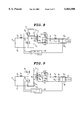
- FIG. 1 is a circuit diagram of a conventional switching power supply
- FIG. 2 is a circuit diagram of another conventional switching power supply
- FIG. 3 is a diagram showing the waveforms of voltages and currents in various parts of the conventional switching power supply shown in FIG. 2;
- FIG. 4 is a diagram showing an output voltage of the conventional switching power supply shown in FIG. 2 with respect to a duty cycle (the ratio of on-time to operating period of a switching element Q 101 ) thereof;
- FIG. 5 is a circuit diagram of a switching power supply according to a first embodiment of the present invention.
- FIG. 6 is a circuit diagram showing a current path in the switching power supply according to the first embodiment of the present invention.
- FIG. 7 is a circuit diagram showing another current path in the switching power supply according to the first embodiment of the present invention.
- FIG. 8 is a circuit diagram showing other current paths in the switching power supply according to the first embodiment of the present invention.
- FIG. 9 is a circuit diagram showing other current paths in the switching power supply according to the first embodiment of the present invention.
- FIG. 10 is a diagram showing the waveforms of voltages and currents in various parts of the switching power supply according to the first embodiment of the present invention.
- FIG. 11 is a diagram showing an output voltage of the switching power supply according to the first embodiment of the present invention with respect to a duty cycle (the ratio of on-time to operating period of a switching element Q 1 ) thereof;
- FIGS. 12a through 12c are circuit diagrams illustrative of the manner in which the switching power supply according to the first embodiment of the present invention operates;
- FIG. 13 is a circuit diagram illustrative of another process of driving synchronous rectifying MOSFETs
- FIG. 14 is a circuit diagram of a switching power supply according to a second embodiment of the present invention.
- FIGS. 15a and 15b are circuit diagrams illustrative of the manner in which the switching power supply according to the second embodiment of the present invention operates;
- FIG. 16 is a circuit diagram of a switching power supply according to a third embodiment of the present invention.
- FIG. 17 is a circuit diagram showing a current path in the switching power supply according to the third embodiment of the present invention.
- FIG. 18 is a circuit diagram showing current paths in the switching power supply according to the third embodiment of the present invention.
- FIG. 19 is a circuit diagram showing current paths in the switching power supply according to the third embodiment of the present invention.
- a switching power supply has an input power supply V in , a pair of input terminals 2 a , 2 b , a first choke coil L 1 , a pair of first and second switching elements Q 1 , Q 2 , a pair of first and second capacitors C 1 , C 2 , a transformer T having a primary winding N 1 and a pair of first and second secondary windings N a , N b , a pair of first and second synchronous rectifying transistors Q 3 , Q 4 , an output filter comprising a second choke coil L 2 and an output capacitor C out , a pair of output terminals 16 a , 16 b , a load 17, and a control circuit 18.
- the input power supply V in has a positive terminal connected to the input terminal 2 a and a negative terminal connected to the input terminal 2 b which is kept at ground potential.
- Each of the first and second switching elements Q 1 , Q 2 comprises an n-channel MOSFET.
- the first switching element Q 1 has a drain terminal connected to the source terminal of the second switching element Q 2 and a source terminal connected to ground.
- the first and second switching elements Q 1 , Q 2 jointly make up a series-connected circuit 41. Diodes which are shown connected respectively across the first and second switching elements Q 1 , Q 2 are parasitic diodes in their MOSFETS.
- the first and second capacitors C 1 , C 2 are connected in series with other and jointly make up a series-connected circuit 42 which has a terminal connected to the drain terminal of the second switching element Q 2 and an opposite terminal connected to ground.
- the series-connected circuit 42 is connected parallel to the series-connected circuit 41, jointly making up a parallel-connected circuit 43.
- the first choke coil L 1 has a terminal connected to the input terminal 2a connected to the positive terminal of the input power supply V in .
- the other terminal of the first choke coil L 1 is connected to the junction between the first and second switching elements Q 1 , Q 2 .
- the junction between the first and second switching elements Q 1 , Q 2 is connected to a terminal of the primary winding N 1 of the transformer T.
- the other terminal of the primary winding N 1 is connected to the junction between the first and second capacitors C 1 , C 2 .
- Each of the first and second synchronous rectifying transistors Q 3 , Q 4 comprises an n-channel MOSFET.
- the first and second secondary windings N a , N b have terminals connected to each other and other terminals connected to the gate terminals of the first and second synchronous rectifying transistors Q 3 , Q 4 .
- the junction between the first secondary winding N a and the gate terminal of the first synchronous rectifying transistor Q 3 is connected to the drain terminal of the second synchronous rectifying transistor Q 4 .
- the junction between the second secondary winding N b and the gate terminal of the second synchronous rectifying transistor Q 4 is connected to the drain terminal of the first synchronous rectifying transistor Q 3 .
- the first and second synchronous rectifying transistors Q 3 , Q 4 have respective source terminals connected to each other, and the output terminal 16 b which is held at ground potential is connected to the junction between the source terminals of the first and second synchronous rectifying transistors Q 3 , Q 4 .
- the first and second secondary windings N a , N b are magnetically coupled to the primary winding N 1 of the transformer T.
- the terminal of the primary winding N 1 which is connected to the first and second switching elements Q 1 , Q 2 is of the same polarity as that of the terminal of the first secondary winding N a which is connected to the second synchronous rectifying transistor Q 4 , and also of the same polarity as that of the terminal of the second secondary winding N b which is connected to the first secondary winding N a .
- the junction between the first and second secondary windings N a , N b is connected to a terminal of the second choke coil L 2 , whose other terminal is connected to the output terminal 16 a which is kept at a positive potential.
- the output capacitor C out is connected between the output terminals 16 a , 16 b .
- the load 17 is also connected between the output terminals 16 a , 16 b parallel to the output capacitor C out .
- the state in which the first and second capacitors C 1 , C 2 are charged is referred to as a steady state.
- the second capacitor C 2 is discharged, causing a current to flow from the drain terminal of the second switching element Q 2 to the source terminal thereof to the primary winding N 1 along a path indicated by J 3 in FIG. 8.
- the first capacitor C 1 When the first switching element Q 1 is turned on and the second switching element Q 2 is turned off in the steady state, the first capacitor C 1 is discharged, causing a current to flow from the drain terminal of the first switching element Q 1 to the source terminal thereof to the primary winding N 1 along a path indicated by J 4 in FIG. 9. At this time, the current flows through the primary winding N 1 in the direction opposite to the direction in which it flows when the second switching element Q 2 is turned on.
- T 31 represents an operating period of the switching elements
- T ON31 represents an on-time of the first switching element Q 1
- T ON32 represents an on-time of the second switching element Q 2
- T off31 , T off32 represent off-times in which both the first and second switching elements Q 1 , Q 2 are turned off.
- the off-times T off31 , T off32 are a period in which both the first and second switching elements Q 1 , Q 2 are prevented from being turned on at the same time, so that series-connected circuit of the first and second capacitors C 1 , C 2 is prevented from being short-circuited.
- the off-times T off31 , T off32 may be of a minimum required period in view of delay times of the first and second switching elements Q 1 , Q 2 upon switching thereof.
- V gs (Q 1 ), V gs (Q 2 ) represent gate drive voltages of the first and second switching elements Q 1 , Q 2 , respectively.
- the first and second switching elements Q 1 , Q 2 are controlled by the control circuit 18 such that when one of the first and second switching elements Q 1 , Q 2 is turned on, the other is turned off, and vice versa except for the short off-times T off31 , T off32 , and that the ratio of the on-time of one of the first and second switching elements Q 1 , Q 2 to the operating period T 31 , i.e., the duty cycle, is varied to produce a constant output voltage V out .
- I(L 1 ) represents a current flowing through the first choke coil L 1
- I(N 1 ) and V(N 1 ) represent a current flowing through and a voltage developed across the primary winding N 1 of the transformer T, respectively
- I(Q 1 ) and I(Q 2 ) represent currents flowing through the first and second switching elements Q 1 , Q 2 , respectively
- V ds (Q 3 ), V ds (Q 4 ) represent drain-to-source voltages of the first and second synchronous rectifying transistors Q 3 , Q 4 , respectively
- V(R) represents a voltage at the junction (point R in FIG. 5) between the first and second secondary windings N a , N b of the transformer T
- I(L 2 ) represents a current flowing through the second choke coil L 2 .
- Operation of the switching power supply shown in FIG. 5 may be considered as a combination of operation of the circuits shown in FIGS. 12a, 12b.
- the second switching element Q 2 is turned off in the on-time of the first switching element Q 1 , and turned on in the off-time of the first switching element Q 1 . Therefore, the second switching element Q 2 operates in the same manner as a commutating diode D 21 in a booster chopper circuit shown in FIG. 12c. Therefore, the circuit shown in FIG. 12a may be replaced with the circuit shown in FIG. 12c, and hence may be regarded as a booster chopper circuit.
- the series-connected circuit of the first and second capacitors C 1 , C 2 shown in FIG. 12b is charged to the single polarity as described above with reference to FIG. 7, it is possible for the first and second capacitors C 1 , C 2 to maintain a certain DC voltage if the first and second capacitors C 1 , C 2 have a sufficiently large capacitance. Consequently, the series-connected circuit of the first and second switching elements Q 1 , Q 2 may be considered as a half-bridge circuit with the series-connected circuit of the first and second capacitors C 1 , C 2 serving as its input power supply.
- the operation of the switching power supply shown in FIG. 5 may be considered as a combination of the operation of the booster chopper circuit shown in FIG. 12a in which the input power supply V in supplies electric energy to the series-connected circuit of the first and second capacitors C 1 , C 2 and the operation of the half-bridge circuit shown in FIG. 12b in which the series-connected circuit of the first and second capacitors C 1 , C 2 supplies electric energy to the load 17 (a quantitative analysis of the above operation will be described later on).
- the first and second capacitors C 1 , C 2 operate with a certain DC voltage because of the operation of the booster chopper circuit shown in FIG. 12a.
- the ratio of the on-time of one of the first switching element Q 1 to the operating period T 31 is varied.
- the current I(L 1 ) flows from the input power supply V in through the first choke coil L 1 to the first switching element Q 1 .
- the current I(L 1 ) flows along the path indicated by J 1 in FIG. 6, and has a waveform those gradient is indicated by V a /L a where V a represents the voltage of the input power supply V in and L a represents the inductance of the first choke coil L 1 .
- the current I(N 1 ) flows from the positive-voltage terminal of the first capacitor C 1 through the primary winding N 1 of the transformer T and the first switching element Q 1 back to the negative-voltage terminal (ground terminal) of the first capacitor C 1 , along the path indicated by J 4 in FIG. 9.
- the current I(N 1 ) flows through the primary winding N 1 , it induces a voltage across the second secondary winding N b , turning on the second synchronous rectifying transistor Q 4 .
- a voltage is then induced across the first secondary winding N a , causing a current to flow along a path indicated by J 6 in FIG. 9.
- the current supplies electric energy to the load 17, and charges the output capacitor C out . It is assumed that at this time the current flows through the primary winding N 1 in a positive direction.
- the current flowing through the primary winding N 1 is equal to the sum of a current converted from the current flowing through the second choke current L 2 with the turns ratio of the transformer T and an magnetizing current of the transformer T.
- the current which is equal to the sum of the current flowing through the first choke coil L 1 along the path indicated by J 1 in FIG. 6 and the current flowing through the primary winding N 1 along the path indicated by J 4 in FIG. 9 flows through the first switching element Q 1 .
- This current has a waveform I(Q 1 ) as shown in FIG. 10.
- the current I (L 1 ) flows through the first choke coil L 1 .
- the current I(L 1 ) is generated by an electromotive force induced across the first choke coil L 1 , and flows from the positive-voltage terminal of the first choke coil L 1 through the second switching element Q 2 , the second capacitor C 2 , the first capacitor C 1 , and the input power supply V in back to the negative-voltage terminal of the first choke coil L 1 , along the path indicated by J 2 in FIG. 7, charging the series-connected circuit of the first and second capacitors C 1 , C 2 .
- This current corresponds to the current flowing through the first choke coil L 1 and the diode D 21 with the first switching element Q 1 being turned off, in the booster chopper circuit shown in FIG. 12c.
- the current has a wavef orm whose gradient is indicated by (V a -V b )/L a where V a represents the voltage of the input power supply V in , L a represents the inductance of the first choke coil L 1 , and V b represents the voltage across the series-connected circuit of the first and second capacitors C 1 , C 2 .
- the second capacitor C 2 is discharged, causing the current I(N 1 ) to flow through the primary winding N 1 of the transformer T, along the path indicated by J 3 in FIG. 8. This current flows from the positive-voltage terminal of the second capacitor C 2 through the second switching element Q 2 and the primary winding N 1 back to the negative-voltage terminal of the second capacitor C 2 .
- the current flowing through the primary winding N 1 is equal to the sum of a current converted from the current flowing through the second choke current L 2 with the turns ratio of the transformer T and an magnetizing current of the transformer T.
- the electromotive force developed across the first choke coil L 1 causes a current to flow through the second switching element Q 2 in the direction to charge the first and second capacitors C 1 , C 2 along the path indicated by J 2 in FIG. 7.
- the current flows from the drain terminal to the source terminal of the second switching element Q 2 along the path indicated by J 3 in FIG. 8 because of the discharging of the second capacitor C 2 , and the current flows from the source terminal to the drain terminal of the second switching element Q 2 along the path indicated by J 2 in FIG. 7 because of the electromotive force developed across the first choke coil L 1 .
- V(N 1 ) represents a voltage developed across the primary winding N 1 of the transformer T.
- This voltage in the on-time T ON31 corresponds to the voltage across the first capacitor C 1 because the first switching element Q 1 is turned on, and in the on-time T ON32 corresponds to the voltage across the second capacitor C 2 because the second switching element Q 2 is turned on.
- V ds (Q 3 ), V ds (Q 4 ) represent, respectively, drain-to-source voltages of the first and second synchronous rectifying transistors Q 3 , Q 4 in FIG. 5. These drain-to-source voltages serve as respective gate drive voltages of the second and first synchronous rectifying transistors Q 4 , Q 3 .
- V(R) represents a voltage at the point R in FIG. 5 between the first and second secondary windings N a , N b of the transformer T, and I(L 2 ) represents a current flowing through the second choke coil L 2 .
- the drain-to-source voltages V ds (Q 3 ), V ds (Q 4 ) are voltages converted from the voltage V(N 1 ) across the primary winding N 1 respectively in the on-times T ON31 , T ON32 with the turns ratio between the primary winding N 1 and the first secondary winding N a (or the second secondary winding N b ).
- the voltage V(R) at the point R is equal to the sum of the drain-to-source voltages V ds (Q 3 ), V ds (Q 4 ).
- V out represents the output voltage between the output terminals 16 a , 16 b .
- the voltage V(R) at the point R and the output voltage V out are applied across the second choke coil L 2 , causing a ripple current I(L 2 ) to flow through the second choke coil L 2 .
- a ripple voltage whose value is substantially determined by the product of the ripple current I(L 2 ) and an equivalent series resistance of the output capacitor C out is generated in the output voltage.
- either one of the drain-to-source voltages V ds (Q 3 ), V ds (Q 4 ) of the first and second synchronous rectifying transistors Q 3 , Q 4 is generated at all times except for the short off-times T off31 , T off32 .
- the switching power supply according to the present invention may thus employ synchronous rectifying transistors having a low dielectric strength and a low on-state resistance.
- V a the voltage of the input power supply V in is represented by V a
- the duty cycles of the respective first and second switching elements Q 1 , Q 2 are represented by D, 1-D, respectively
- the voltages across the first and second capacitors C 1 , C 2 are represented by V(C 1 ), V(C 2 ), respectively
- the turns ratio between the primary winding N 1 and the first secondary winding N a (or the second secondary winding N b ) is represented by n: 1
- the drain-to-source voltages of the first and second synchronous rectifying transistors Q 3 , Q 4 are represented by V ds (Q 3 ), V ds (Q 4 ), respectively
- the output voltage between the output terminals 16 a , 16 b is represented by V out .
- the output voltage between the output terminals 16 a , 16 b is of a value produced by averaging the voltage at the point R with the output filter, and the voltage at the point R is equal to the sum of the drain-to-source voltages V ds (Q 3 ), V ds (Q 4 ) of the first and second synchronous rectifying transistors Q 3 , Q 4 . Therefore, if the switching period is represented by T 0 , then the following equation (7) is satisfied: ##EQU1##
- V ds (Q 3 ), V ds (Q 4 ) are variable about the value V a /n while keeping the rectangular waveform even when the input and output conditions are varied, the first and second synchronous rectifying transistors Q 3 , Q 4 are not required to be of large dielectric strength and large on-state resistance unlike those of the conventional switching power supply.
- V ds (Q 3 ), V ds (Q 4 ) are equal to each other (actually, they are slightly different from each other as the numbers of turns of the transformer T are integers) means that any changes in the voltage V(R) at the point R are very small.
- the second choke coil L 2 may be small, and any power loss caused by the second choke coil L 2 may be small, so that the switching power supply may be highly efficient.
- the output filter is designed taking into account variations in the input and output conditions, but the second choke coil L 2 may still be small.
- I(N 1 ) represents a current flowing through the primary winding N 1 of the transformer T. Since the transformer T has a leakage inductance, the off-times T off31 , T off31 in which both the first and second switching elements Q 1 , Q 2 are turned off may be adjusted appropriately such that after one of the first and second switching elements Q 1 , Q 2 is turned off and before the other of the first and second switching elements Q 1 , Q 2 is turned on, a current due to the leakage inductance discharges the parasitic capacitor between the drain and source of the other switching element. As a result, the switching power supply can operate as a ZVS (Zero Voltage Switching) power supply.
- ZVS Zero Voltage Switching
- either one of the first and second synchronous rectifying transistors Q 3 , Q 4 is energized at all times except for the short off-times T off31 , T off32 , i.e., the synchronous rectifying transistor through which the current flowing through the second choke coil L 2 flows is energized, and their applied drain-to-source voltage is low. Therefore, the first and second synchronous rectifying transistors Q 3 , Q 4 may be of small dielectric strength and small on-state resistance, and at the same time the output filter may be small and any power loss caused by the output filter may be small.
- the switching power supply is highly efficient in operation.
- each of the first and second switching elements Q 1 , Q 2 comprises an n-channel MOSFET.
- one or both of the first and second switching elements Q 1 , Q 2 may comprise a p-channel MOSFET.
- each of the first and second switching elements Q 1 , Q 2 is not limited to a MOSFET, but may comprise an IGBT.
- the series-connected circuit of the input power supply V in and the first choke coil L 1 may be connected between the drain and source of the second switching element Q 2 rather than between the drain and source of the first switching element Q 1 .
- the switching power supply thus modified operates in the same manner as described above except that the first and second switching elements Q 1 , Q 2 are switched around.
- the full-wave rectifier circuit comprising two rectifiers is connected to the secondary windings N a , N b of the transformer T.
- a half-wave rectifier circuit with one of the two rectifiers used as a freewheeling rectifier may be connected to the secondary windings N a , N b of the transformer T, or a full-wave rectifier circuit comprising a bridge of four rectifiers may be connected to the secondary windings N a , N b of the transformer T.
- each of the first and second synchronous rectifying transistors Q 3 , Q 4 in the switching power supply shown in FIG. 5 is turned on by the drain-to-source voltage of the other first and second synchronous rectifying transistors Q 3 , Q 4 .
- the gate terminal of each of the first and second synchronous rectifying transistors Q 3 , Q 4 may be turned on by a voltage obtained from the windings of the transformer T.
- FIG. 13 Another process of driving the first and second synchronous rectifying transistors Q 3 , Q 4 is shown in FIG. 13.
- a switching power supply shown in FIG. 13 operates in a manner equivalent to the switching power supply shown in FIG. 5.
- the source terminal of a second switching element Q 52 is connected to the drain terminal of the first switching element Q 1 , and the first and second switching element Q 1 , Q 52 are connected in series with each other, thus jointly making up a series-connected circuit 44.
- a second capacitor C 52 is connected parallel to the series-connected circuit 44, jointly making up a parallel-connected circuit 45.
- the switching power supply shown in FIG. 14 is equivalent to the switching power supply shown in FIG. 5, and operates in the same manner as the switching power supply shown in FIG. 5.
- the switching power supply shown in FIG. 14 is equivalent to the switching power supply shown in FIG. 5 for the reasons which will be described below with reference to FIGS. 15a and 15b.
- FIGS. 15a and 15b show half-bridge circuits which correspond to the switching power supplies according to the first and second embodiments, respectively.
- the second switching element Q 2 and the second capacitor C 2 are connected in series with each other.
- the second switching element Q 52 and the second capacitor C 52 are connected in series with each other. If the capacitor C 52 shown in FIG. 15b has a capacitance equivalent to the combined capacitance of the series-connected capacitors C 1 , C 2 , then the capacitor C 52 shown in FIG. 15b may be replaced with a capacitor C 100 shown in FIG. 15b which has the same capacitance as the capacitance of the capacitor C 2 .
- the switching power supply shown in FIG. 14 offers the same advantages as those of the switching power supply according to the second embodiment shown in FIG. 5.
- FIG. 16 shows a switching power supply according to a third embodiment of the present invention.
- the first choke coil L 1 has a terminal connected to the input terminal 2 a which is connected to the positive-voltage terminal of the input power supply V in .
- the other terminal of the first choke coil L 1 is connected to a terminal of the primary winding N 1 of a transformer T.
- the other terminal of the primary winding N 1 is connected by the first capacitor C 1 to the input terminal 2 b which is kept at ground potential.
- the primary winding N 1 and the first capacitor C 1 jointly make up a series-connected circuit 47.
- the first switching element Q 1 which comprises an n-channel MOSFET is connected parallel to the series-connected circuit 47.
- the first switching element Q 1 has a source terminal connected to ground and a drain terminal connected to the junction between the first choke coil L 1 and the primary winding N 1 .
- the parts connected to the first and second secondary windings N a , N b of the transformer T are identical to those of the switching power supply according to the first embodiment.
- the first and second secondary windings N a , N b are magnetically coupled to the primary winding N 1 of the transformer T.
- the switching power supply shown in FIG. 16 additionally has a tertiary winding N 3 magnetically coupled to the primary winding N 1 and the first and second secondary windings N a , N b .
- the tertiary winding N 3 has a terminal connected by a second capacitor C 62 to the drain terminal of a second switching element Q 62 which comprises an n-channel MOSFET.
- the other terminal of the tertiary winding N 3 is connected to the source terminal of the second switching element Q 62 .
- the tertiary winding N 3 and the second capacitor C 62 jointly make up a series-connected circuit 48.
- the second switching element Q 62 is connected parallel to the series-connected circuit 48.
- the terminal of the tertiary winding N 3 which is connected to the second switching element Q 62 is of the same polarity as that of the terminal of the primary winding N 1 which is connected to the drain terminal of the first switching element Q 1 .
- the current starts to flow from the terminal of the first choke coil L 1 where a positive voltage is induced, and flows through the primary winding N 1 , thereby inducing voltages across the respective first and second secondary windings N a , N b .
- the current flowing through the primary winding N 1 flows into the first capacitor C 1 , thus charging first capacitor C 1 .
- the current thus passes through the input power supply V in , and flows back to the terminal of the first choke coil L 1 where a negative voltage is induced.
- the first and second capacitors C 1 , C 62 are thus charged when the first and second switching element Q 1 , Q 62 are alternately rendered conductive.
- the state in which the first and second capacitors C 1 , C 62 are charged is referred to as a steady state.
- a current flows along a path indicated by J 15 in FIG. 18 due to the discharging of the second capacitor C 62 at the same time that the current flows along the path indicated by J 14 .
- the current flowing along the path indicated by J 15 is opposite in direction to the current flowing along the path indicated by J 14 , and these current cancel out each other.
- the induced voltages are of such polarity that the second synchronous rectifying transistor Q 4 is turned on, and a current flows from the terminal of the first secondary windings N a where a positive voltage is induced, through the second choke coil L 2 , the output capacitor C out (or the load), the source terminal of the second synchronous rectifying transistor Q 4 , and the drain terminal thereof, to the terminal of the first secondary windings N a where a negative voltage is induced, along a path indicated by J 13 in FIG. 18.
- the first and second synchronous rectifying transistors Q 3 , Q 4 are also alternately rendered conductive, supplying electric energy to the output capacitor C out and the load. While voltages are being induced across the first and second secondary windings N a , N b , the first synchronous rectifying transistor Q 3 or the second synchronous rectifying transistor Q 4 is rendered conductive, with no current flowing through the internal parasitic diode. This operation is the same as the operation of the switching power supplies according to the first and second embodiments.
- the switching power supply according to the third embodiment shown in FIG. 16 voltages can be converted from the secondary side to the primary side of the transformer T with the turns ratio of the transformer T.
- the switching power supply according to the third embodiment has an equivalent circuit which is the same as the equivalent circuit of the switching power supply according to the first embodiment shown in FIG. 5.
- the switching power supply according to the third embodiment shown in FIG. 16 offers the same advantages as those of the switching power supply according to the first embodiment shown in FIG. 5.
- either one of the first and second synchronous rectifying transistors Q 3 , Q 4 is energized at all times except for the short off-times T off31 , T off32 . Therefore, the first and second synchronous rectifying transistors Q 3 , Q 4 may be of small dielectric strength and small on-state resistance, and at the same time the output filter may be small. Consequently, the switching power supply may be highly efficient in operation.
Landscapes
- Engineering & Computer Science (AREA)
- Power Engineering (AREA)
- Dc-Dc Converters (AREA)
- Rectifiers (AREA)
Applications Claiming Priority (2)
| Application Number | Priority Date | Filing Date | Title |
|---|---|---|---|
| JP07493098A JP3673075B2 (ja) | 1998-03-09 | 1998-03-09 | スイッチング電源装置 |
| JP10-074930 | 1998-03-09 |
Publications (1)
| Publication Number | Publication Date |
|---|---|
| US6064580A true US6064580A (en) | 2000-05-16 |
Family
ID=13561576
Family Applications (1)
| Application Number | Title | Priority Date | Filing Date |
|---|---|---|---|
| US09/262,917 Expired - Lifetime US6064580A (en) | 1998-03-09 | 1999-03-05 | Switching power supply |
Country Status (6)
| Country | Link |
|---|---|
| US (1) | US6064580A (fr) |
| EP (1) | EP0942519B1 (fr) |
| JP (1) | JP3673075B2 (fr) |
| CA (1) | CA2264443C (fr) |
| DE (1) | DE69901918T2 (fr) |
| HK (1) | HK1022218A1 (fr) |
Cited By (49)
| Publication number | Priority date | Publication date | Assignee | Title |
|---|---|---|---|---|
| US6188586B1 (en) * | 2000-04-21 | 2001-02-13 | Lucent Technologies Inc. | Asymmetrical half-bridge power converter having reduced input ripple and method of manufacturing the same |
| US6198644B1 (en) * | 1998-09-03 | 2001-03-06 | Nagano Japan Radio Co., Ltd. | Rectifying/smoothing circuit and double-ended converter |
| US6246598B1 (en) * | 2000-08-02 | 2001-06-12 | Polarity, Inc. | High-voltage modulator system |
| US6288919B1 (en) * | 1999-12-16 | 2001-09-11 | Chippower.Com, Inc. | Single stage AC/DC converter high frequency AC distribution systems |
| US6349044B1 (en) * | 1999-09-09 | 2002-02-19 | Virginia Tech Intellectual Properties, Inc. | Zero voltage zero current three level dc-dc converter |
| US6353544B1 (en) * | 2000-07-27 | 2002-03-05 | Hua-In Co., Ltd. | Flyback converter with synchronous rectifier |
| US20020122321A1 (en) * | 2001-03-01 | 2002-09-05 | Alain Chapuis | Voltage converter |
| US6483722B2 (en) * | 2000-11-10 | 2002-11-19 | Fuji Electric Co., Ltd. | DC/DC converter and control method thereof |
| US6483205B1 (en) * | 2000-07-28 | 2002-11-19 | Ricky Martin | Distributed transformer control |
| US6545883B2 (en) * | 2001-05-07 | 2003-04-08 | Artesyn Technologies, Inc. | Integrated boost-asymmetrical half-bridge converter |
| US20030086282A1 (en) * | 2001-11-02 | 2003-05-08 | Jianhong Zeng | DC-to-DC converter |
| US6621722B1 (en) * | 1998-12-07 | 2003-09-16 | Lovoltech, Inc. | Rectifier circuits with low forward voltage JFET device |
| US6650552B2 (en) * | 2001-05-25 | 2003-11-18 | Tdk Corporation | Switching power supply unit with series connected converter circuits |
| US6696706B1 (en) | 2002-10-22 | 2004-02-24 | Lovoltech, Inc. | Structure and method for a junction field effect transistor with reduced gate capacitance |
| US6734715B1 (en) | 1999-11-29 | 2004-05-11 | Lovoltech, Inc. | Two terminal rectifier using normally off JFET |
| US20040145930A1 (en) * | 2002-12-27 | 2004-07-29 | Yamaha Corporation | Power supply circuit |
| US6777722B1 (en) | 2002-07-02 | 2004-08-17 | Lovoltech, Inc. | Method and structure for double dose gate in a JFET |
| US20040179378A1 (en) * | 2003-03-11 | 2004-09-16 | Denso Corporation | Insulating switching DC/DC converter |
| US6807073B1 (en) | 2001-05-02 | 2004-10-19 | Oltronics, Inc. | Switching type power converter circuit and method for use therein |
| US20050068792A1 (en) * | 2003-09-30 | 2005-03-31 | Masayuki Yasumura | Switching power supply circuit |
| US6900506B1 (en) | 2002-04-04 | 2005-05-31 | Lovoltech, Inc. | Method and structure for a high voltage junction field effect transistor |
| US6921932B1 (en) | 2002-05-20 | 2005-07-26 | Lovoltech, Inc. | JFET and MESFET structures for low voltage, high current and high frequency applications |
| US20050237771A1 (en) * | 2004-04-22 | 2005-10-27 | Patent-Treuhand-Gesellschaft Fur Elektrisch Gluhlampen Mbh | Circuit for converting an AC voltage to a DC voltage |
| US7038260B1 (en) | 2003-03-04 | 2006-05-02 | Lovoltech, Incorporated | Dual gate structure for a FET and method for fabricating same |
| US7075132B1 (en) | 2002-12-30 | 2006-07-11 | Lovoltech, Inc. | Programmable junction field effect transistor and method for programming the same |
| US20060226819A1 (en) * | 2005-03-31 | 2006-10-12 | Ming Xu | Self-driven scheme for synchronous rectifier |
| US20070103005A1 (en) * | 2005-11-08 | 2007-05-10 | Toshio Nagasawa | Switching power supply device, semiconductor integrated circuit device and power supply device |
| US7262461B1 (en) | 2002-05-20 | 2007-08-28 | Qspeed Semiconductor Inc. | JFET and MESFET structures for low voltage, high current and high frequency applications |
| US7268378B1 (en) | 2002-05-29 | 2007-09-11 | Qspeed Semiconductor Inc. | Structure for reduced gate capacitance in a JFET |
| US20070247123A1 (en) * | 2006-04-19 | 2007-10-25 | International Rectifier Corporation | Single stage integrated boost inverter motor drive circuit |
| US20080049456A1 (en) * | 2005-10-19 | 2008-02-28 | Murata Manufacturing Co., Ltd. | Synchronous rectifying forward converter |
| US20080049455A1 (en) * | 2006-02-09 | 2008-02-28 | Murata Manufacturing Co., Ltd. | Forward converter with synchronous rectification |
| US20080285311A1 (en) * | 2007-05-18 | 2008-11-20 | Sanken Electric Co., Ltd. | Dc-dc converter |
| US20090219006A1 (en) * | 2008-02-28 | 2009-09-03 | Fuji Electric Device Technology Co., Ltd. | Electric power converter |
| US20100232189A1 (en) * | 2009-03-13 | 2010-09-16 | American Power Conversion Corporation | Method for portioning output current of a dc-dc converter |
| US20110058396A1 (en) * | 2006-01-19 | 2011-03-10 | Conergy Ag | Flyback-type inverter circuit for network supply or for network-independent operation |
| US20110188269A1 (en) * | 2010-01-29 | 2011-08-04 | Murata Manufacturing Co., Ltd. | Switching power-supply apparatus |
| US20120033453A1 (en) * | 2010-04-30 | 2012-02-09 | Infineon Technologies Ag | Controller for a Resonant Switched-Mode Power Converter |
| US20130294114A1 (en) * | 2012-05-07 | 2013-11-07 | Sanken Electric Co., Ltd. | Direct-Current Converter |
| US20140268908A1 (en) * | 2013-03-15 | 2014-09-18 | Solarbridge Technologies, Inc. | Converter topologies |
| CN104094378A (zh) * | 2012-02-29 | 2014-10-08 | 英福康有限责任公司 | 质谱仪阴极的电压供应装置 |
| US20150043263A1 (en) * | 2013-08-11 | 2015-02-12 | Anatoly Diber | Dc-ac inverter having controlled magnetization reversal of isolation transformer core |
| US20150333640A1 (en) * | 2013-02-28 | 2015-11-19 | Telefonaktiebolaget L M Ericsson (Publ) | Forward-Flyback Topology Switched Mode Power Supply |
| US20160036337A1 (en) * | 2013-05-21 | 2016-02-04 | Murata Manufacturing Co | Switching power supply apparatus |
| US9973073B2 (en) * | 2016-08-24 | 2018-05-15 | Omron Automotive Electronics Co., Ltd. | Voltage conversion device that ensures supply of power to a controller even if the input voltage decreases |
| US20180191260A1 (en) * | 2017-01-05 | 2018-07-05 | Rohm Co., Ltd. | Rectifier ic and isolated switching power supply using same |
| US20180198373A1 (en) * | 2016-07-07 | 2018-07-12 | Huawei Technologies Co., Ltd. | Four-switch three phase dc-dc resonant converter |
| US10103638B1 (en) * | 2017-08-09 | 2018-10-16 | Infineon Technologies Austria Ag | Flyback converter with capacitor module and switching module |
| US11139746B2 (en) * | 2019-01-31 | 2021-10-05 | Rockwell Automation Technologies, Inc. | Power converter with reduced switch mode power supply EMI |
Families Citing this family (15)
| Publication number | Priority date | Publication date | Assignee | Title |
|---|---|---|---|---|
| US6169683B1 (en) * | 1999-10-07 | 2001-01-02 | Ericsson Inc. | Resonant gate drive for synchronous rectifiers |
| US6188592B1 (en) * | 1999-11-05 | 2001-02-13 | Ericsson Inc. | Externally-driven scheme for synchronous rectification |
| WO2001044655A2 (fr) | 1999-12-17 | 2001-06-21 | Fleck Carl M | Interrupteur d'allumage controlable |
| US7733069B2 (en) * | 2000-09-29 | 2010-06-08 | Canon Kabushiki Kaisha | Power converting apparatus and power generating apparatus |
| JP2003009530A (ja) * | 2001-06-21 | 2003-01-10 | Shindengen Electric Mfg Co Ltd | スイッチング電源安定化回路 |
| EP1646122A1 (fr) * | 2004-10-06 | 2006-04-12 | Nokia Corporation | Panneau à circuit imprimé multicouche portant un circuit de charge de batterie et une bobine d'induction |
| JP4335871B2 (ja) * | 2005-12-27 | 2009-09-30 | 新電元工業株式会社 | スイッチング電源装置及びサージ吸収回路 |
| JP4812433B2 (ja) * | 2006-01-13 | 2011-11-09 | 新電元工業株式会社 | スイッチング電源装置 |
| JP4689648B2 (ja) * | 2007-08-31 | 2011-05-25 | 新電元工業株式会社 | スイッチング電源装置 |
| JP5103671B2 (ja) * | 2008-02-06 | 2012-12-19 | 新電元工業株式会社 | トランスおよびこのトランスを備えたスイッチング電源装置 |
| JP5012715B2 (ja) * | 2008-07-25 | 2012-08-29 | 株式会社デンソー | Dc−dcコンバータ |
| JP5284188B2 (ja) * | 2009-06-16 | 2013-09-11 | 株式会社東芝 | スイッチング電源装置 |
| JP5831275B2 (ja) * | 2012-02-10 | 2015-12-09 | 日産自動車株式会社 | 電力変換装置及びその駆動方法 |
| WO2016017257A1 (fr) * | 2014-07-31 | 2016-02-04 | 株式会社村田製作所 | Dispositif de conversion de courant et système de transmission d'énergie sans fil |
| DE102018218367A1 (de) * | 2018-10-26 | 2020-04-30 | Conti Temic Microelectronic Gmbh | Gleichspannungswandler |
Citations (6)
| Publication number | Priority date | Publication date | Assignee | Title |
|---|---|---|---|---|
| US4441146A (en) * | 1982-02-04 | 1984-04-03 | Vicor Corporation | Optimal resetting of the transformer's core in single ended forward converters |
| EP0165087A1 (fr) * | 1984-04-16 | 1985-12-18 | Alcatel N.V. | Alimentation de puissance à découpage |
| US5243509A (en) * | 1990-08-14 | 1993-09-07 | General Electric Cgr S.A. | Variable frequency resonant converter |
| EP0670624A1 (fr) * | 1994-03-03 | 1995-09-06 | Alcatel Converters | Alimentation à découpage adaptée pour permettre des commutations sous tension réduite |
| US5822198A (en) * | 1996-06-21 | 1998-10-13 | Lucent Technologies Inc. | Single stage power converter and method of operation thereof |
| US5907481A (en) * | 1997-10-31 | 1999-05-25 | Telefonaktiebolaget Lm Ericsson | Double ended isolated D.C.--D.C. converter |
-
1998
- 1998-03-09 JP JP07493098A patent/JP3673075B2/ja not_active Expired - Lifetime
-
1999
- 1999-03-05 US US09/262,917 patent/US6064580A/en not_active Expired - Lifetime
- 1999-03-05 CA CA002264443A patent/CA2264443C/fr not_active Expired - Fee Related
- 1999-03-08 DE DE69901918T patent/DE69901918T2/de not_active Expired - Lifetime
- 1999-03-08 EP EP99104598A patent/EP0942519B1/fr not_active Expired - Lifetime
-
2000
- 2000-02-25 HK HK00101169A patent/HK1022218A1/xx not_active IP Right Cessation
Patent Citations (6)
| Publication number | Priority date | Publication date | Assignee | Title |
|---|---|---|---|---|
| US4441146A (en) * | 1982-02-04 | 1984-04-03 | Vicor Corporation | Optimal resetting of the transformer's core in single ended forward converters |
| EP0165087A1 (fr) * | 1984-04-16 | 1985-12-18 | Alcatel N.V. | Alimentation de puissance à découpage |
| US5243509A (en) * | 1990-08-14 | 1993-09-07 | General Electric Cgr S.A. | Variable frequency resonant converter |
| EP0670624A1 (fr) * | 1994-03-03 | 1995-09-06 | Alcatel Converters | Alimentation à découpage adaptée pour permettre des commutations sous tension réduite |
| US5822198A (en) * | 1996-06-21 | 1998-10-13 | Lucent Technologies Inc. | Single stage power converter and method of operation thereof |
| US5907481A (en) * | 1997-10-31 | 1999-05-25 | Telefonaktiebolaget Lm Ericsson | Double ended isolated D.C.--D.C. converter |
Non-Patent Citations (6)
| Title |
|---|
| Eiji Sakai et al.; "synchronous Rectifier for Low Voltage Switching Converter"; Technical Report of IEICE; PE95-14 (1995-07); p9-p16.(with translation of relevant passages). |
| Eiji Sakai et al.; synchronous Rectifier for Low Voltage Switching Converter ; Technical Report of IEICE; PE95 14 (1995 07); p9 p16.(with translation of relevant passages). * |
| Ionel Dan Jitaru et al.; "Increasing the Utilization of the Transformer's Magnetic Core by Using Quasi-integrated Magnetics"; HFPC Power Conversion (Sep. 1996); p238-p908. |
| Ionel Dan Jitaru et al.; Increasing the Utilization of the Transformer s Magnetic Core by Using Quasi integrated Magnetics ; HFPC Power Conversion (Sep. 1996); p238 p908. * |
| J.A. Cobos, et al.; "Optimized Synchronous Rectification Stage for Low Output voltage (3.3V) DC/DC Conversion"; IEEE Power Electronics Specialists Conference (PESC) (1994); p902-p908, May 1994. |
| J.A. Cobos, et al.; Optimized Synchronous Rectification Stage for Low Output voltage (3.3V) DC/DC Conversion ; IEEE Power Electronics Specialists Conference (PESC) (1994); p902 p908, May 1994. * |
Cited By (79)
| Publication number | Priority date | Publication date | Assignee | Title |
|---|---|---|---|---|
| US6198644B1 (en) * | 1998-09-03 | 2001-03-06 | Nagano Japan Radio Co., Ltd. | Rectifying/smoothing circuit and double-ended converter |
| US6621722B1 (en) * | 1998-12-07 | 2003-09-16 | Lovoltech, Inc. | Rectifier circuits with low forward voltage JFET device |
| US6349044B1 (en) * | 1999-09-09 | 2002-02-19 | Virginia Tech Intellectual Properties, Inc. | Zero voltage zero current three level dc-dc converter |
| US6734715B1 (en) | 1999-11-29 | 2004-05-11 | Lovoltech, Inc. | Two terminal rectifier using normally off JFET |
| US6288919B1 (en) * | 1999-12-16 | 2001-09-11 | Chippower.Com, Inc. | Single stage AC/DC converter high frequency AC distribution systems |
| US6188586B1 (en) * | 2000-04-21 | 2001-02-13 | Lucent Technologies Inc. | Asymmetrical half-bridge power converter having reduced input ripple and method of manufacturing the same |
| US6353544B1 (en) * | 2000-07-27 | 2002-03-05 | Hua-In Co., Ltd. | Flyback converter with synchronous rectifier |
| US6483205B1 (en) * | 2000-07-28 | 2002-11-19 | Ricky Martin | Distributed transformer control |
| US6246598B1 (en) * | 2000-08-02 | 2001-06-12 | Polarity, Inc. | High-voltage modulator system |
| US6483722B2 (en) * | 2000-11-10 | 2002-11-19 | Fuji Electric Co., Ltd. | DC/DC converter and control method thereof |
| US20020122321A1 (en) * | 2001-03-01 | 2002-09-05 | Alain Chapuis | Voltage converter |
| US6657872B2 (en) * | 2001-03-01 | 2003-12-02 | Power-One Ag | Voltage converter |
| US20050036340A1 (en) * | 2001-05-02 | 2005-02-17 | Oltronics | Switching type power converter circuit and method for use therein |
| US7002815B2 (en) | 2001-05-02 | 2006-02-21 | Oltronics, Inc. | Switching type power converter circuit and method for use therein |
| US6807073B1 (en) | 2001-05-02 | 2004-10-19 | Oltronics, Inc. | Switching type power converter circuit and method for use therein |
| US6545883B2 (en) * | 2001-05-07 | 2003-04-08 | Artesyn Technologies, Inc. | Integrated boost-asymmetrical half-bridge converter |
| US6650552B2 (en) * | 2001-05-25 | 2003-11-18 | Tdk Corporation | Switching power supply unit with series connected converter circuits |
| US20040070994A1 (en) * | 2001-05-25 | 2004-04-15 | Tdk Corp. | Switching power supply unit |
| US6888728B2 (en) | 2001-05-25 | 2005-05-03 | Tdk Corporation | Switching power supply unit |
| US20030086282A1 (en) * | 2001-11-02 | 2003-05-08 | Jianhong Zeng | DC-to-DC converter |
| US6778410B2 (en) * | 2001-11-02 | 2004-08-17 | Delta Electronics, Inc. | DC-to-DC converter |
| US6900506B1 (en) | 2002-04-04 | 2005-05-31 | Lovoltech, Inc. | Method and structure for a high voltage junction field effect transistor |
| US7262461B1 (en) | 2002-05-20 | 2007-08-28 | Qspeed Semiconductor Inc. | JFET and MESFET structures for low voltage, high current and high frequency applications |
| US6921932B1 (en) | 2002-05-20 | 2005-07-26 | Lovoltech, Inc. | JFET and MESFET structures for low voltage, high current and high frequency applications |
| US7268378B1 (en) | 2002-05-29 | 2007-09-11 | Qspeed Semiconductor Inc. | Structure for reduced gate capacitance in a JFET |
| US6777722B1 (en) | 2002-07-02 | 2004-08-17 | Lovoltech, Inc. | Method and structure for double dose gate in a JFET |
| US6696706B1 (en) | 2002-10-22 | 2004-02-24 | Lovoltech, Inc. | Structure and method for a junction field effect transistor with reduced gate capacitance |
| US7209374B2 (en) * | 2002-12-27 | 2007-04-24 | Yamaha Corporation | Capacitor-input positive and negative power supply circuit |
| US20040145930A1 (en) * | 2002-12-27 | 2004-07-29 | Yamaha Corporation | Power supply circuit |
| US7075132B1 (en) | 2002-12-30 | 2006-07-11 | Lovoltech, Inc. | Programmable junction field effect transistor and method for programming the same |
| US7655964B1 (en) | 2002-12-30 | 2010-02-02 | Qspeed Semiconductor Inc. | Programmable junction field effect transistor and method for programming same |
| US7038260B1 (en) | 2003-03-04 | 2006-05-02 | Lovoltech, Incorporated | Dual gate structure for a FET and method for fabricating same |
| US6961254B2 (en) | 2003-03-11 | 2005-11-01 | Denso Corporation | Insulating switching DC/DC converter |
| US20040179378A1 (en) * | 2003-03-11 | 2004-09-16 | Denso Corporation | Insulating switching DC/DC converter |
| US20050068792A1 (en) * | 2003-09-30 | 2005-03-31 | Masayuki Yasumura | Switching power supply circuit |
| US7218534B2 (en) * | 2003-09-30 | 2007-05-15 | Sony Corporation | Switching power supply circuit |
| US20050237771A1 (en) * | 2004-04-22 | 2005-10-27 | Patent-Treuhand-Gesellschaft Fur Elektrisch Gluhlampen Mbh | Circuit for converting an AC voltage to a DC voltage |
| US7265525B2 (en) * | 2005-03-31 | 2007-09-04 | Virginia Tech Intellectual Properties, Inc. | Self-driven scheme for synchronous rectifier having no body diode |
| US20060226819A1 (en) * | 2005-03-31 | 2006-10-12 | Ming Xu | Self-driven scheme for synchronous rectifier |
| US20080049456A1 (en) * | 2005-10-19 | 2008-02-28 | Murata Manufacturing Co., Ltd. | Synchronous rectifying forward converter |
| US7480158B2 (en) * | 2005-10-19 | 2009-01-20 | Murata Manufacturing Co., Ltd. | Synchronous rectifying forward converter |
| US7408388B2 (en) * | 2005-11-08 | 2008-08-05 | Renesas Technology Corp. | Switching power supply device, semiconductor integrated circuit device and power supply device |
| US20070103005A1 (en) * | 2005-11-08 | 2007-05-10 | Toshio Nagasawa | Switching power supply device, semiconductor integrated circuit device and power supply device |
| US20110058396A1 (en) * | 2006-01-19 | 2011-03-10 | Conergy Ag | Flyback-type inverter circuit for network supply or for network-independent operation |
| US20080049455A1 (en) * | 2006-02-09 | 2008-02-28 | Murata Manufacturing Co., Ltd. | Forward converter with synchronous rectification |
| US7423889B2 (en) * | 2006-02-09 | 2008-09-09 | Murata Manufacturing Co., Ltd. | Forward converter with synchronous rectification |
| US20070247123A1 (en) * | 2006-04-19 | 2007-10-25 | International Rectifier Corporation | Single stage integrated boost inverter motor drive circuit |
| US7589986B2 (en) * | 2006-04-19 | 2009-09-15 | International Rectifier Corporation | Single stage integrated boost inverter motor drive circuit |
| US20080285311A1 (en) * | 2007-05-18 | 2008-11-20 | Sanken Electric Co., Ltd. | Dc-dc converter |
| US7589980B2 (en) * | 2007-05-18 | 2009-09-15 | Sanken Electric Co., Ltd. | DC-DC converter |
| US20090219006A1 (en) * | 2008-02-28 | 2009-09-03 | Fuji Electric Device Technology Co., Ltd. | Electric power converter |
| US20100232189A1 (en) * | 2009-03-13 | 2010-09-16 | American Power Conversion Corporation | Method for portioning output current of a dc-dc converter |
| US20110188269A1 (en) * | 2010-01-29 | 2011-08-04 | Murata Manufacturing Co., Ltd. | Switching power-supply apparatus |
| US8837174B2 (en) * | 2010-01-29 | 2014-09-16 | Murata Manufacturing Co., Ltd. | Switching power-supply apparatus including switching elements having a low threshold voltage |
| US20120033453A1 (en) * | 2010-04-30 | 2012-02-09 | Infineon Technologies Ag | Controller for a Resonant Switched-Mode Power Converter |
| US8665611B2 (en) * | 2010-04-30 | 2014-03-04 | Infineon Technologies Ag | Controller for a resonant switched-mode power converter |
| CN104094378A (zh) * | 2012-02-29 | 2014-10-08 | 英福康有限责任公司 | 质谱仪阴极的电压供应装置 |
| CN104094378B (zh) * | 2012-02-29 | 2016-08-17 | 英福康有限责任公司 | 质谱仪阴极的电压供应装置 |
| US20150028743A1 (en) * | 2012-02-29 | 2015-01-29 | Inficon Gmbh | Device for supplying voltage to the cathode of a mass spectrometer |
| RU2638303C2 (ru) * | 2012-02-29 | 2017-12-13 | Инфикон Гмбх | Устройство для питания напряжением катода масс-спектрометра |
| US9530634B2 (en) * | 2012-02-29 | 2016-12-27 | Inficon Gmbh | Device for supplying voltage to the cathode of a mass spectrometer |
| US20130294114A1 (en) * | 2012-05-07 | 2013-11-07 | Sanken Electric Co., Ltd. | Direct-Current Converter |
| US9246393B2 (en) * | 2012-05-07 | 2016-01-26 | Sanken Electric Co., Ltd. | Direct-current converter capable of increasing operating frequency |
| US9559601B2 (en) * | 2013-02-28 | 2017-01-31 | Telefonaktiebolaget Lm Ericsson (Publ) | Forward-flyback topology switched mode power supply |
| US20150333640A1 (en) * | 2013-02-28 | 2015-11-19 | Telefonaktiebolaget L M Ericsson (Publ) | Forward-Flyback Topology Switched Mode Power Supply |
| US20140268908A1 (en) * | 2013-03-15 | 2014-09-18 | Solarbridge Technologies, Inc. | Converter topologies |
| US9584044B2 (en) * | 2013-03-15 | 2017-02-28 | Sunpower Corporation | Technologies for converter topologies |
| US9748851B2 (en) * | 2013-05-21 | 2017-08-29 | Murata Manufacturing Co., Ltd. | Switching power supply apparatus with snubber circuit |
| US20160036337A1 (en) * | 2013-05-21 | 2016-02-04 | Murata Manufacturing Co | Switching power supply apparatus |
| US20150043263A1 (en) * | 2013-08-11 | 2015-02-12 | Anatoly Diber | Dc-ac inverter having controlled magnetization reversal of isolation transformer core |
| US9407170B2 (en) * | 2013-08-11 | 2016-08-02 | Anatoly Diber | DC-AC inverter having controlled magnetization reversal of isolation transformer core |
| US20180198373A1 (en) * | 2016-07-07 | 2018-07-12 | Huawei Technologies Co., Ltd. | Four-switch three phase dc-dc resonant converter |
| CN109874380A (zh) * | 2016-07-07 | 2019-06-11 | 华为技术有限公司 | 四开关三相dc-dc谐振转换器 |
| US10715050B2 (en) * | 2016-07-07 | 2020-07-14 | Huawei Technologies Co., Ltd. | Four-switch three phase DC-DC resonant converter |
| US9973073B2 (en) * | 2016-08-24 | 2018-05-15 | Omron Automotive Electronics Co., Ltd. | Voltage conversion device that ensures supply of power to a controller even if the input voltage decreases |
| US20180191260A1 (en) * | 2017-01-05 | 2018-07-05 | Rohm Co., Ltd. | Rectifier ic and isolated switching power supply using same |
| US10381940B2 (en) * | 2017-01-05 | 2019-08-13 | Rohm Co., Ltd. | Rectifier IC and isolated switching power supply using same |
| US10103638B1 (en) * | 2017-08-09 | 2018-10-16 | Infineon Technologies Austria Ag | Flyback converter with capacitor module and switching module |
| US11139746B2 (en) * | 2019-01-31 | 2021-10-05 | Rockwell Automation Technologies, Inc. | Power converter with reduced switch mode power supply EMI |
Also Published As
| Publication number | Publication date |
|---|---|
| EP0942519B1 (fr) | 2002-06-26 |
| DE69901918D1 (de) | 2002-08-01 |
| CA2264443A1 (fr) | 1999-09-09 |
| HK1022218A1 (en) | 2000-07-28 |
| JP3673075B2 (ja) | 2005-07-20 |
| JPH11262263A (ja) | 1999-09-24 |
| DE69901918T2 (de) | 2003-02-06 |
| CA2264443C (fr) | 2006-02-14 |
| EP0942519A1 (fr) | 1999-09-15 |
Similar Documents
| Publication | Publication Date | Title |
|---|---|---|
| US6064580A (en) | Switching power supply | |
| US5907481A (en) | Double ended isolated D.C.--D.C. converter | |
| US7825765B2 (en) | DC-DC converter | |
| US5726869A (en) | Synchronous rectifier type DC-to-DC converter in which a saturable inductive device is connected in series with a secondary-side switching device | |
| US6757184B2 (en) | Step-down buck converter with full bridge circuit | |
| JP2005503099A (ja) | 調整された2つの出力を有する電力コンバータ | |
| JPS59178970A (ja) | 調節されたdc−dcコンバ−タ | |
| US20060104097A1 (en) | DC converter | |
| US6504735B2 (en) | Regulated voltage reducing high-voltage isolated DC/DC converter system | |
| US6181578B1 (en) | Synchronous rectifier drive mechanism for resonant reset forward converters | |
| JP4123231B2 (ja) | 直流変換装置 | |
| JP3790256B2 (ja) | スイッチング電源装置の制御方法 | |
| US11641165B2 (en) | Flyback converter and method of operating the same | |
| JP4337376B2 (ja) | 直流変換装置 | |
| JP4329450B2 (ja) | 直流変換装置 | |
| JPWO2004001937A1 (ja) | Dc−dcコンバータ | |
| JP2000125560A (ja) | スイッチング電源装置 | |
| JPH10136646A (ja) | 同期整流器 | |
| US11632051B2 (en) | Flyback converter and method of operating the same | |
| JP4265199B2 (ja) | 直流変換装置 | |
| JP3557385B2 (ja) | スイッチング電源装置 | |
| JP2002199726A (ja) | スイッチング電源装置 | |
| JP2005020948A (ja) | Dc−dcコンバータ | |
| JP2004320916A (ja) | Dc−dcコンバータ | |
| JP2001086747A (ja) | 電源装置 |
Legal Events
| Date | Code | Title | Description |
|---|---|---|---|
| AS | Assignment |
Owner name: SHINDENGEN ELECTRIC MANUFACTURING CO., LTD., JAPAN Free format text: ASSIGNMENT OF ASSIGNORS INTEREST;ASSIGNORS:WATANABE, HARUO;HATAKEYAMA, HARUHIKO;REEL/FRAME:009814/0765 Effective date: 19990127 |
|
| STCF | Information on status: patent grant |
Free format text: PATENTED CASE |
|
| FEPP | Fee payment procedure |
Free format text: PAT HOLDER NO LONGER CLAIMS SMALL ENTITY STATUS, ENTITY STATUS SET TO UNDISCOUNTED (ORIGINAL EVENT CODE: STOL); ENTITY STATUS OF PATENT OWNER: LARGE ENTITY |
|
| REFU | Refund |
Free format text: REFUND - SURCHARGE, PETITION TO ACCEPT PYMT AFTER EXP, UNINTENTIONAL (ORIGINAL EVENT CODE: R2551); ENTITY STATUS OF PATENT OWNER: LARGE ENTITY |
|
| FPAY | Fee payment |
Year of fee payment: 4 |
|
| FEPP | Fee payment procedure |
Free format text: ENTITY STATUS SET TO UNDISCOUNTED (ORIGINAL EVENT CODE: BIG.); ENTITY STATUS OF PATENT OWNER: LARGE ENTITY |
|
| FPAY | Fee payment |
Year of fee payment: 8 |
|
| REMI | Maintenance fee reminder mailed | ||
| FPAY | Fee payment |
Year of fee payment: 12 |