US5732465A - Method of manufacturing one side resin sealing type semiconductor devices - Google Patents
Method of manufacturing one side resin sealing type semiconductor devices Download PDFInfo
- Publication number
- US5732465A US5732465A US08/502,811 US50281195A US5732465A US 5732465 A US5732465 A US 5732465A US 50281195 A US50281195 A US 50281195A US 5732465 A US5732465 A US 5732465A
- Authority
- US
- United States
- Prior art keywords
- carrier frame
- circuit board
- resin
- circuit boards
- wiring patterns
- Prior art date
- Legal status (The legal status is an assumption and is not a legal conclusion. Google has not performed a legal analysis and makes no representation as to the accuracy of the status listed.)
- Expired - Fee Related
Links
- 229920005989 resin Polymers 0.000 title claims abstract description 111
- 239000011347 resin Substances 0.000 title claims abstract description 111
- 239000004065 semiconductor Substances 0.000 title claims abstract description 85
- 238000007789 sealing Methods 0.000 title claims abstract description 57
- 238000004519 manufacturing process Methods 0.000 title claims abstract description 28
- 238000000034 method Methods 0.000 claims description 50
- 229910000679 solder Inorganic materials 0.000 claims description 21
- 239000010410 layer Substances 0.000 claims description 16
- 238000003825 pressing Methods 0.000 claims description 10
- 238000000576 coating method Methods 0.000 claims description 9
- 239000012790 adhesive layer Substances 0.000 claims description 8
- 239000011248 coating agent Substances 0.000 claims description 8
- 230000000630 rising effect Effects 0.000 claims description 5
- 238000004382 potting Methods 0.000 claims description 4
- 230000002093 peripheral effect Effects 0.000 claims 2
- 238000005476 soldering Methods 0.000 abstract description 3
- 239000000463 material Substances 0.000 description 6
- 238000000465 moulding Methods 0.000 description 6
- 238000005304 joining Methods 0.000 description 5
- 238000010521 absorption reaction Methods 0.000 description 3
- 238000005520 cutting process Methods 0.000 description 3
- XEEYBQQBJWHFJM-UHFFFAOYSA-N Iron Chemical compound [Fe] XEEYBQQBJWHFJM-UHFFFAOYSA-N 0.000 description 2
- 239000000853 adhesive Substances 0.000 description 2
- 239000002313 adhesive film Substances 0.000 description 2
- 230000000694 effects Effects 0.000 description 2
- 229910015365 Au—Si Inorganic materials 0.000 description 1
- 239000004593 Epoxy Substances 0.000 description 1
- 230000001070 adhesive effect Effects 0.000 description 1
- 230000015572 biosynthetic process Effects 0.000 description 1
- 239000000919 ceramic Substances 0.000 description 1
- 230000005496 eutectics Effects 0.000 description 1
- 229920006015 heat resistant resin Polymers 0.000 description 1
- 229910052742 iron Inorganic materials 0.000 description 1
- 239000002184 metal Substances 0.000 description 1
- 229910052751 metal Inorganic materials 0.000 description 1
- 238000012986 modification Methods 0.000 description 1
- 230000004048 modification Effects 0.000 description 1
- 238000007747 plating Methods 0.000 description 1
- 239000012858 resilient material Substances 0.000 description 1
- 239000003566 sealing material Substances 0.000 description 1
- 229910052710 silicon Inorganic materials 0.000 description 1
- 239000010703 silicon Substances 0.000 description 1
- 239000002699 waste material Substances 0.000 description 1
- XLYOFNOQVPJJNP-UHFFFAOYSA-N water Substances O XLYOFNOQVPJJNP-UHFFFAOYSA-N 0.000 description 1
Images


Classifications
-
- H—ELECTRICITY
- H01—ELECTRIC ELEMENTS
- H01L—SEMICONDUCTOR DEVICES NOT COVERED BY CLASS H10
- H01L21/00—Processes or apparatus adapted for the manufacture or treatment of semiconductor or solid state devices or of parts thereof
- H01L21/02—Manufacture or treatment of semiconductor devices or of parts thereof
- H01L21/04—Manufacture or treatment of semiconductor devices or of parts thereof the devices having at least one potential-jump barrier or surface barrier, e.g. PN junction, depletion layer or carrier concentration layer
- H01L21/50—Assembly of semiconductor devices using processes or apparatus not provided for in a single one of the subgroups H01L21/06 - H01L21/326, e.g. sealing of a cap to a base of a container
- H01L21/56—Encapsulations, e.g. encapsulation layers, coatings
- H01L21/568—Temporary substrate used as encapsulation process aid
-
- H—ELECTRICITY
- H01—ELECTRIC ELEMENTS
- H01L—SEMICONDUCTOR DEVICES NOT COVERED BY CLASS H10
- H01L21/00—Processes or apparatus adapted for the manufacture or treatment of semiconductor or solid state devices or of parts thereof
- H01L21/02—Manufacture or treatment of semiconductor devices or of parts thereof
- H01L21/04—Manufacture or treatment of semiconductor devices or of parts thereof the devices having at least one potential-jump barrier or surface barrier, e.g. PN junction, depletion layer or carrier concentration layer
- H01L21/50—Assembly of semiconductor devices using processes or apparatus not provided for in a single one of the subgroups H01L21/06 - H01L21/326, e.g. sealing of a cap to a base of a container
- H01L21/56—Encapsulations, e.g. encapsulation layers, coatings
- H01L21/565—Moulds
-
- H—ELECTRICITY
- H01—ELECTRIC ELEMENTS
- H01L—SEMICONDUCTOR DEVICES NOT COVERED BY CLASS H10
- H01L23/00—Details of semiconductor or other solid state devices
- H01L23/28—Encapsulations, e.g. encapsulating layers, coatings, e.g. for protection
- H01L23/31—Encapsulations, e.g. encapsulating layers, coatings, e.g. for protection characterised by the arrangement or shape
- H01L23/3107—Encapsulations, e.g. encapsulating layers, coatings, e.g. for protection characterised by the arrangement or shape the device being completely enclosed
- H01L23/3121—Encapsulations, e.g. encapsulating layers, coatings, e.g. for protection characterised by the arrangement or shape the device being completely enclosed a substrate forming part of the encapsulation
- H01L23/3128—Encapsulations, e.g. encapsulating layers, coatings, e.g. for protection characterised by the arrangement or shape the device being completely enclosed a substrate forming part of the encapsulation the substrate having spherical bumps for external connection
-
- H—ELECTRICITY
- H01—ELECTRIC ELEMENTS
- H01L—SEMICONDUCTOR DEVICES NOT COVERED BY CLASS H10
- H01L2224/00—Indexing scheme for arrangements for connecting or disconnecting semiconductor or solid-state bodies and methods related thereto as covered by H01L24/00
- H01L2224/01—Means for bonding being attached to, or being formed on, the surface to be connected, e.g. chip-to-package, die-attach, "first-level" interconnects; Manufacturing methods related thereto
- H01L2224/42—Wire connectors; Manufacturing methods related thereto
- H01L2224/47—Structure, shape, material or disposition of the wire connectors after the connecting process
- H01L2224/48—Structure, shape, material or disposition of the wire connectors after the connecting process of an individual wire connector
- H01L2224/4805—Shape
- H01L2224/4809—Loop shape
- H01L2224/48091—Arched
-
- H—ELECTRICITY
- H01—ELECTRIC ELEMENTS
- H01L—SEMICONDUCTOR DEVICES NOT COVERED BY CLASS H10
- H01L2224/00—Indexing scheme for arrangements for connecting or disconnecting semiconductor or solid-state bodies and methods related thereto as covered by H01L24/00
- H01L2224/01—Means for bonding being attached to, or being formed on, the surface to be connected, e.g. chip-to-package, die-attach, "first-level" interconnects; Manufacturing methods related thereto
- H01L2224/42—Wire connectors; Manufacturing methods related thereto
- H01L2224/47—Structure, shape, material or disposition of the wire connectors after the connecting process
- H01L2224/48—Structure, shape, material or disposition of the wire connectors after the connecting process of an individual wire connector
- H01L2224/481—Disposition
- H01L2224/48151—Connecting between a semiconductor or solid-state body and an item not being a semiconductor or solid-state body, e.g. chip-to-substrate, chip-to-passive
- H01L2224/48221—Connecting between a semiconductor or solid-state body and an item not being a semiconductor or solid-state body, e.g. chip-to-substrate, chip-to-passive the body and the item being stacked
- H01L2224/48225—Connecting between a semiconductor or solid-state body and an item not being a semiconductor or solid-state body, e.g. chip-to-substrate, chip-to-passive the body and the item being stacked the item being non-metallic, e.g. insulating substrate with or without metallisation
- H01L2224/48227—Connecting between a semiconductor or solid-state body and an item not being a semiconductor or solid-state body, e.g. chip-to-substrate, chip-to-passive the body and the item being stacked the item being non-metallic, e.g. insulating substrate with or without metallisation connecting the wire to a bond pad of the item
-
- H—ELECTRICITY
- H01—ELECTRIC ELEMENTS
- H01L—SEMICONDUCTOR DEVICES NOT COVERED BY CLASS H10
- H01L24/00—Arrangements for connecting or disconnecting semiconductor or solid-state bodies; Methods or apparatus related thereto
- H01L24/01—Means for bonding being attached to, or being formed on, the surface to be connected, e.g. chip-to-package, die-attach, "first-level" interconnects; Manufacturing methods related thereto
- H01L24/42—Wire connectors; Manufacturing methods related thereto
- H01L24/47—Structure, shape, material or disposition of the wire connectors after the connecting process
- H01L24/48—Structure, shape, material or disposition of the wire connectors after the connecting process of an individual wire connector
-
- H—ELECTRICITY
- H01—ELECTRIC ELEMENTS
- H01L—SEMICONDUCTOR DEVICES NOT COVERED BY CLASS H10
- H01L2924/00—Indexing scheme for arrangements or methods for connecting or disconnecting semiconductor or solid-state bodies as covered by H01L24/00
- H01L2924/0001—Technical content checked by a classifier
- H01L2924/00014—Technical content checked by a classifier the subject-matter covered by the group, the symbol of which is combined with the symbol of this group, being disclosed without further technical details
-
- H—ELECTRICITY
- H01—ELECTRIC ELEMENTS
- H01L—SEMICONDUCTOR DEVICES NOT COVERED BY CLASS H10
- H01L2924/00—Indexing scheme for arrangements or methods for connecting or disconnecting semiconductor or solid-state bodies as covered by H01L24/00
- H01L2924/01—Chemical elements
- H01L2924/01078—Platinum [Pt]
-
- H—ELECTRICITY
- H01—ELECTRIC ELEMENTS
- H01L—SEMICONDUCTOR DEVICES NOT COVERED BY CLASS H10
- H01L2924/00—Indexing scheme for arrangements or methods for connecting or disconnecting semiconductor or solid-state bodies as covered by H01L24/00
- H01L2924/01—Chemical elements
- H01L2924/01079—Gold [Au]
-
- H—ELECTRICITY
- H01—ELECTRIC ELEMENTS
- H01L—SEMICONDUCTOR DEVICES NOT COVERED BY CLASS H10
- H01L2924/00—Indexing scheme for arrangements or methods for connecting or disconnecting semiconductor or solid-state bodies as covered by H01L24/00
- H01L2924/013—Alloys
- H01L2924/0132—Binary Alloys
- H01L2924/01322—Eutectic Alloys, i.e. obtained by a liquid transforming into two solid phases
-
- H—ELECTRICITY
- H01—ELECTRIC ELEMENTS
- H01L—SEMICONDUCTOR DEVICES NOT COVERED BY CLASS H10
- H01L2924/00—Indexing scheme for arrangements or methods for connecting or disconnecting semiconductor or solid-state bodies as covered by H01L24/00
- H01L2924/15—Details of package parts other than the semiconductor or other solid state devices to be connected
- H01L2924/181—Encapsulation
-
- Y—GENERAL TAGGING OF NEW TECHNOLOGICAL DEVELOPMENTS; GENERAL TAGGING OF CROSS-SECTIONAL TECHNOLOGIES SPANNING OVER SEVERAL SECTIONS OF THE IPC; TECHNICAL SUBJECTS COVERED BY FORMER USPC CROSS-REFERENCE ART COLLECTIONS [XRACs] AND DIGESTS
- Y10—TECHNICAL SUBJECTS COVERED BY FORMER USPC
- Y10T—TECHNICAL SUBJECTS COVERED BY FORMER US CLASSIFICATION
- Y10T29/00—Metal working
- Y10T29/49—Method of mechanical manufacture
- Y10T29/49002—Electrical device making
- Y10T29/49117—Conductor or circuit manufacturing
- Y10T29/49124—On flat or curved insulated base, e.g., printed circuit, etc.
- Y10T29/4913—Assembling to base an electrical component, e.g., capacitor, etc.
- Y10T29/49146—Assembling to base an electrical component, e.g., capacitor, etc. with encapsulating, e.g., potting, etc.
-
- Y—GENERAL TAGGING OF NEW TECHNOLOGICAL DEVELOPMENTS; GENERAL TAGGING OF CROSS-SECTIONAL TECHNOLOGIES SPANNING OVER SEVERAL SECTIONS OF THE IPC; TECHNICAL SUBJECTS COVERED BY FORMER USPC CROSS-REFERENCE ART COLLECTIONS [XRACs] AND DIGESTS
- Y10—TECHNICAL SUBJECTS COVERED BY FORMER USPC
- Y10T—TECHNICAL SUBJECTS COVERED BY FORMER US CLASSIFICATION
- Y10T29/00—Metal working
- Y10T29/51—Plural diverse manufacturing apparatus including means for metal shaping or assembling
- Y10T29/5136—Separate tool stations for selective or successive operation on work
- Y10T29/5137—Separate tool stations for selective or successive operation on work including assembling or disassembling station
Definitions
- the present invention relates to a method for manufacturing a one side resin sealing type semiconductor device in which a circuit board such as a BGA (Ball Grid Array) is used, and also relates to a carrier frame used for manufacturing such a one side resin sealing type semiconductor device.
- a circuit board such as a BGA (Ball Grid Array)
- An over molded BGA type semiconductor device is manufactured in such a manner that a semiconductor element is mounted on a printed board, and one of the surfaces of the printed board on which the semiconductor element is mounted is sealed with resin, and then solder balls are attached onto the other surface of the board.
- a printed board of a large size on both surfaces of which the predetermined wiring patterns are provided (these wiring patterns on the both surfaces being connected by through-hole patterns), is cut into several rectangular pieces, and each of the thus obtained rectangular printed boards 5 is conveyed to the processes of mounting a semiconductor element, bonding wires, sealing with resin and attaching solder balls. In this way, the product of the semiconductor device is manufactured.
- the semiconductor elements are mounted on one of the surfaces of the printed board and subjected to resin molding, and then external terminals such as solder balls are joined onto the other surface of the printed board. After that, the printed board is cut off to obtain several BGAs. Accordingly, the area of the printed board outside the cutting position is not used for the product of the semiconductor device, so that material of the periphery of the rectangular printed board is wasted. Besides, when the rectangular printed board is made of a printed board of a large size, it is necessary to provide a flap for cutting of the printed board. Therefore, material of the printed board corresponding to the flap for cutting is wasted in the process of making the printed board.
- the base board is individually formed, being separated into each piece of the product size, and each piece is conveyed one by one so that a semiconductor element is mounted on each base board and then each base board is subjected to resin molding.
- a semiconductor element is mounted on each base board and then each base board is subjected to resin molding.
- a method of manufacturing one side resin sealing type semiconductor devices of the present invention is characterized in that: a circuit board, the size of which is formed into an individual piece of the product, is disposed in a carrier frame having a predetermined through-hole shape in such a manner that the circuit board is opposed to the through-hole; and the circuit board is conveyed to each process by each carrier frame, so that the processes of mounting a semiconductor element, wire bonding and resin sealing are effected.
- On the circuit board there is provided a wiring pattern for joining the semiconductor mount face to the external terminals, and it is possible to mount a semiconductor element, to bond wires, to seal the circuit board with resin, and to join the external terminals under the condition that the circuit board is supported by the carrier frame.
- the carrier frame is formed into a rectangle so that a plurality of individual pieces of circuit boards can be supported by the carrier frame, and the individual circuit boards are positioned and supported by the support means so that they can be positioned in the carrier frame.
- the circuit board is engaged with the carrier frame by an engaging piece and engaging portion, the circuit board is conveyed while the carrier frame is reversed.
- the method of manufacturing one side resin sealing type semiconductor devices of the present invention it is possible to effectively reduce the manufacturing cost of the one side resin sealing type semiconductor device.
- the existing apparatus can be used for the effective manufacture of the one side resin sealing type semiconductor device.
- the carrier frame of the present invention it is possible to preferably manufacture the one side resin sealing type semiconductor device.
- FIGS. 1(a) to 1(d) are schematic illustrations for explaining the method of manufacturing one side resin sealing type semiconductor devices
- FIG. 2 is a schematic cross-sectional view for explaining the method of manufacturing one side resin sealing type semiconductor devices
- FIG. 3 is a schematic plan view showing a state in which the circuit board is attached to the carrier frame having a groove
- FIG. 4 is a schematic perspective view showing a state in which a plurality of circuit boards are attached to the carrier frame
- FIG. 5 is a schematic cross-sectional view showing a support means for supporting the circuit board by the carrier frame
- FIG. 6 is a schematic plan view showing the support means for supporting the circuit board
- FIGS. 7(a) to 7(c) are schematic illustrations showing an embodiment of the method of manufacturing one side resin sealing type semiconductor devices
- FIGS. 8(a) to 8(c) are schematic illustrations showing another embodiment of the method of manufacturing one side resin sealing type semiconductor devices
- FIG. 9 is a cross-sectional view showing an embodiment of the carrier frame on which a resilient layer is provided.
- FIG. 10 is a partially enlarged cross-sectional view showing a state of resin sealing in which the circuit board is attached to the carrier frame provided with a resilient layer;
- FIG. 11 is a cross-sectional view showing a state in which the circuit board is attached to the carrier frame provided with an adhesive layer;
- FIG. 12 is a schematic perspective view showing a state in which the circuit boards are attached to the carrier frame
- FIGS. 13, 14 and 15 are schematic cross-sectional views showing support means for supporting the circuit board by the carrier frame
- FIGS. 16(a) to 16(d) are schematic illustrations showing an embodiment of the method of manufacturing one type of side resin sealing type semiconductor devices
- FIGS. 17(a) to 17(c) are schematic illustrations showing an embodiment of the method of manufacturing one type of side resin sealing type semiconductor devices
- FIGS. 18(a) to 18(c) are schematic illustrations showing another embodiment of the method of manufacturing one type of side resin sealing type semiconductor devices
- FIGS. 19 and 20 are cross-sectional views showing a state of resin sealing in which the circuit board is attached to the carrier frame having fixing pins;
- FIG. 21 is a plan view showing a state in which the circuit boards are attached to the carrier frame
- FIGS. 22(a) and 22(b) are schematic cross-sectional views showing other examples of the fixing pins formed on the carrier frame; and FIG. 23 is a plan view of a one side resin sealing type semiconductor device.
- FIGS. 1(a) to 1(d) are views showing a series of assembly processes of BGA type semiconductor devices, which is an embodiment of the method of manufacturing one side resin sealing type semiconductor devices.
- a semiconductor element 20 is mounted on a circuit board 10, which is a body of a BGA, and the circuit board 10 is subjected to resin sealing after wire bonding, and then solder balls 30 are joined to the circuit board 10.
- individual pieces of circuit boards 10, the sizes of which are the same as those of the products, are used, and a plurality of such circuit boards 10 are disposed in a carrier frame 12, and the individual carrier frame 12 is conveyed to each process so that the circuit board 10 is subjected to the predetermined processing.
- the carrier frame 12 is made of a metal, such as iron, or heat-resistant resin.
- circuit board 10 One side of the circuit board 10 is a semiconductor element mount face 10a. On the semiconductor element mount face 10a, there is provided a wiring pattern which is subjected to wire bonding with a mounted semiconductor element. On the other side of the circuit board 10, there is provided a wiring pattern to which external terminals are joined. In a portion of the carrier frame 12 where the circuit board 10 is disposed, there is provided a through-hole 13 used for processing so that the predetermined processing can be conducted under the condition that the circuit board 10 is attached to the carrier frame 12.
- circuit board 10 it is possible to process the circuit board 10 either when the circuit board 10 is attached onto an upper side of the carrier frame 12 or when the circuit board 10 is attached onto a lower side of the carrier frame 12.
- the circuit board 10 is supported on the lower face of the carrier frame 12.
- the circuit board 10 is attached to the carrier frame 12 while the semiconductor element mount face 10a comes into contact with the carrier frame 12.
- FIG. 4 shows a state in which a plurality of above-mentioned circuit boards 10 are supported by the carrier frame 12.
- three sheets of circuit boards 10 are supported by a single carrier frame 12, and rectangular through-holes 13 are formed at positions of the carrier frame 12 where the circuit boards 10 are disposed.
- the through-holes 13 are provided for mounting the semiconductor elements 20 on the semiconductor element mount face 10a of the circuit board 10 so that the semiconductor elements 20 can be electrically connected with the wiring pattern by means of wire bonding.
- the through-holes 13 are provided for defining resin seal regions into which resin is supplied when using resin sealing.
- Reference numeral 28' denotes a region to which a runner passage 28 is to be arranged.
- FIG. 5 is a schematic illustration to explain a support means for positioning and supporting the circuit board 10 by the carrier frame 12.
- FIG. 6 is a schematic illustration for explaining a plan arrangement of the support means.
- the carrier frame 12 includes: engaging pieces 14 which are a support means for supporting three sides of the circuit board 10; and an engaging portion 16 for supporting the remaining one side of the circuit board 10. As illustrated in FIG.
- the engaging piece 14 is made in such a manner that a portion of the sheet member composing the carrier frame 12 is cut and raised, and a fore end of the engaging piece 14 is open outwardly so that the circuit board 10 can easily be arranged, and further a middle portion of the engaging piece 14 is a little constricted in accordance with the thickness of the circuit board 10, so that the circuit board 10 can be easily engaged with the carrier frame 12.
- the circuit board 10 is engaged with the engaging piece 14 and positioned in the carrier frame 12 by the engaging piece 14.
- the engaging portion 16 is made in such a manner that a portion of the sheet member composing the carrier frame 12 is cut and raised.
- the engaging portion 16 includes a rising piece portion 16a at which the sheet member is cut and raised, and a pair of pressing piece portions 16b provided at the free end of the rising piece portion 16a.
- the pressing piece portions 16b support the circuit board 10 by pressing the circuit board 10 against the carrier frame 12. As illustrated in FIG. 6, the pressing piece portions 16b are disposed on the respective sides of the rising piece portion 16a. A side of the pressing piece portion 16b where the circuit board 10 is pressed is curved outwardly in an inclined condition so that the circuit board 10 can be easily attached to and detached from the carrier frame 12.
- reference numeral 18 is a pilot hole used when the carrier frame 12 is fed by a predetermined distance in the processing, further the pilot hole 18 is used for positioning the carrier frame 12 in the apparatus.
- FIGS. 1(a) to 1(d) the manufacturing process shown in FIGS. 1(a) to 1(d) is explained as follows.
- the circuit board 10 is positioned in the carrier frame 12 by the support means described above while the semiconductor element mount face 10a of the circuit board 10 comes into contact with the carrier frame 12, and the semiconductor element 20 is fixed onto the semiconductor element mount face 10a.
- a heater block 22 is made to contact a lower face of the circuit board 10, and the fixing portion is heated by the heater block 22 and joined by means of Au-Si eutectic joining or soldering.
- the semiconductor element 20 may be fixed onto the circuit board 10 with thermo-setting resin at room temperature.
- the semiconductor element 20 is electrically connected with the wiring pattern by means of wire bonding.
- Reference numeral 24 is a bonder used for wire bonding.
- the electrical connection between the semiconductor element 20 and the wiring pattern on the circuit board 10 is not limited to the wire bonding, but other methods such as a gang bonding method or a flip chip bonding method may be adaptable.
- FIG. 1(c) shows a state in which the circuit board 10 and the carrier frame 12 are clamped by the metallic molds 26a and 26b, and the circuit board 10 is sealed with resin. Since the resin sealing operation is conducted on one side of the circuit board 10 on which the semiconductor element 20 is mounted, a cavity portion is formed in the metallic mold 26a on the upper side, and a runner passage 28 is provided on the upper face of the carrier frame 12 and the cavity portion is filled with resin. As illustrated in FIG.
- the circuit board 10 is detached from the carrier frame 12 in the after-process (such as, after external connector terminals, i.e., solder balls 30, are attached), it is necessary to design the metallic mold 26a in such a manner that the resin formation region is not larger than the region of the through-hole 13.
- resin molding is conducted under the condition that the circuit board 10 is disposed on the lower side of the carrier frame 12, as illustrated in FIG. 1(c)
- only the runner passage 28 adheres to the carrier frame 12, and no resin adheres to the circuit board 10 when resin is molded for sealing.
- solder balls 30 used as the external terminals to be connected with an assembly board are attached onto the lower face of the circuit board 10. Since the circuit board 10 is only resiliently held by the carrier frame 12 through the support means, it is easy to detach the circuit board 10 from the carrier frame 12, and a single body of the BGA product can be provided.
- reference numeral 29 is a resin sealing portion.
- solder balls are used as the external terminals, however, it is possible to use lead pins as the external terminals of the one side resin sealing type semiconductor device.
- a printed board is used for the circuit board 10 of the one side resin sealing type semiconductor device.
- the water-absorption and moisture-absorption properties of the printed board are higher than those of the ceramic package, and moisture tends to be absorbed from a side portion since the side of the circuit board 10 is exposed.
- the following resin sealing method may be adopted: As illustrated in FIGS. 2 and 3, grooves 15 are formed on the face of the carrier frame 12 on which the circuit board 10 is supported, wherein the grooves 15 communicate the corners of the through-hole 13 with the periphery of the circuit board 10.
- the metallic mold 26b on the lower side is formed in such a manner that the size of a recess portion in which the circuit board 10 is set is a little larger than the outer size of the circuit board 10, so that resin flows from the grooves 15 into a clearance formed between the side wall of the recess portion of the metallic mold 26b and the side of the circuit board 10 when resin is supplied for sealing.
- FIG. 2 is a cross-sectional view taken along line A--A in FIG. 3.
- the carrier frame 12 is conveyed under the condition that the circuit boards 10 are set upwardly, however, depending upon the apparatus, it is preferable that the carrier frame 12 is reversed in the process.
- FIGS. 7(a) to 7(c) are views showing an embodiment in which the processing is conducted as follows.
- the semiconductor element 20 is mounted on the circuit board 10 and subjected to wire bonding.
- the carrier frame 12 is reversed, and the circuit board 10 is sealed with resin and the solder balls 30 are joined.
- the circuit board 10 is located on the upper side of the carrier frame 12 in the case of resin sealing. Therefore, the circuit board 10 can be more positively supported, and further the solder balls 30 are joined on the upper side of the circuit board 10. Accordingly, it is easy to join the solder balls 30 onto the circuit board 10.
- FIGS. 8(a) to 8(c) are views showing an embodiment in which the processes from the beginning to the resin sealing are conducted under the condition that the circuit board 10 is supported on the lower face of the carrier frame 12, and after the resin sealing has been completed, the carrier frame 12 is reversed and the solder balls 30 are joined.
- the semiconductor element 20 is sealed with resin by means of resin molding in which the metallic molds 26a, 26b are used.
- sealing of the semiconductor element 20 is not necessarily limited to resin molding.
- the carrier frame 12 is reversed only once during the processing, however, it is possible to further reverse the carrier frame 12.
- the carrier frame after the resin sealing has been completed, it is possible to reverse the carrier frame again so that the solder ball joining face is set downwardly and the solder balls 30 are joined.
- FIG. 9 is a view showing another embodiment in which the circuit board 10 is supported in such a manner that the semiconductor element mount face 10a comes into contact with the carrier frame 12.
- the carrier frame 12 of this embodiment is characterized in that the resilient layers 12a, 12b are provided on both sides of the base material of the carrier frame 12.
- FIG. 10 is a view showing a state in which the circuit board 10 is attached to the carrier frame 12 provided with the resilient layers 12a and 12b, and the metallic molds 26a and 26b are clamped so as to seal the circuit board 10 with resin.
- the circuit board 10 is clamped together with the carrier frame 12 by the metallic molds 26a and 26b, and then sealed with resin. Since both sides of the carrier frame 12 of this embodiment are covered with the resilient layers 12a and 12b, the circuit board 10 can be appropriately clamped by the metallic molds 26a and 26b and sealed with resin.
- the resilient layers 12a and 12b provided on both sides of the carrier frame 12 function in such a manner that the clamping force appropriately acts on the circuit board 10 so that resin can be prevented from leaking out from the resin sealing region. Due to the cushioning effect of the resilient layers 12a and 12b, it is possible to prevent the occurrence of damage such as cracks and dents of a resist layer provided on the surface of the circuit board 10 when the circuit board 10 is strongly clamped by the metallic molds 26a and 26b through the carrier frame 12.
- the material of the resilient layers 12a and 12b is not particularly limited, but a resilient material such as heat resistant silicon may be appropriately used.
- the resilient layers 12a and 12b are provided on both sides of the base material of the carrier frame 12, however, when the resilient layers 12a and 12b are provided at least on the faces of the carrier frame 12 with which the circuit board 10 comes into contact, it is possible to prevent the occurrence of leakage of resin and damage of the resist layer of the wiring pattern.
- the resilient layers 12a and 12b may be provided over the entire surface of the carrier frame 12. Alternatively the resilient layers 12a and 12b may be provided only in a portion where the circuit board 10 comes into contact with the metallic mold 26a as illustrated in FIG. 9.
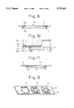
- FIG. 11 is a view showing still another embodiment of the carrier frame 12.
- This embodiment is characterized in that: an adhesive layer 12c is provided in the periphery of the through-hole 13 on the carrier frame 12 where the circuit board 10 is supported, and the circuit board 10 adheres to the carrier frame 12 and is supported.
- the circuit board 10 is supported by the engaging pieces 14.
- the adhesive layer 12c has the same cushioning effect as that of the resilient layers 12a and 12b of the above embodiment.
- the adhesive layer 12c may be formed in such a manner that an adhesive agent is coated on the face of the carrier frame 12, or an adhesive film is adhered onto the face of the carrier frame 12.
- Examples of usable adhesive films are: an ultraviolet ray hardening film, and a track dry epoxy film. Since the circuit board 10 is separated from the carrier frame 12 after the completion of assembly, it is preferable that the adhesive layer 12c has a feature in which the circuit board 12 can be easily detached from the adhesive layer 12c after the completion of assembly.
- circuit board 10 is supported on the upper face of the carrier frame 12 and subjected to the necessary assembly process.
- the circuit board 10 is attached in such a manner that the semiconductor element mount face comes into contact with the carrier frame 12 and then the circuit board 10 is subjected to resin sealing.
- the circuit board 10 is supported in such a manner that a joining face onto which the solder balls 30 are joined is contacted with the carrier frame 12.
- FIG. 12 is a view showing a state in which the circuit board 10 is attached onto the upper face of the carrier frame 12.
- the through-hole 13 is formed in the carrier frame 12, and the circuit board 10 is positioned by the engaging pieces 14.
- FIGS. 13, 14 and 15 show the other embodiments in which the circuit board 10 is supported on the upper face of the rectangular carrier frame 12.
- FIG. 13 The embodiment shown in FIG. 13 is composed as follows. A sheet member composing the carrier frame 12 is cut and raised so as to form the engaging piece 14. When this engaging piece 14 comes into contact with the side of the circuit board 10, the circuit board 10 can be positioned with respect to the tarrier frame 12. A resilient movable engaging piece 32 composed differently from the carrier frame 12 is fixed to the lower face of the carrier frame 12 by means of soldering, and the circuit board 10 is held being pressed against the carrier frame 12 by the movable engaging piece 32.
- the movable engaging piece 32 When the circuit board 10 is attached to and detached from the carrier frame 12, the movable engaging piece 32 is pushed open. Since the carrier frame 12 is composed differently from the movable engaging piece 32, the number of parts is increased, however, the circuit board 10 can be positively supported by the resilient movable engaging piece 32.
- the embodiment shown in FIG. 14 is composed as follows.
- a movable engaging piece 33 pressing the circuit board 10 against the carrier frame 12 is made when a sheet member composing the carrier frame 12 is cut and raised relatively long, and an inner face of the movable engaging piece 33 presses an upper edge of the side of the circuit board 10, so that the circuit board 10 is supported by the carrier frame 12.
- the movable engaging piece 33 can be easily pushed open, and the circuit board 10 can be easily attached to and detached from the carrier frame 12. Since the movable engaging piece 33 is composed integrally with the carrier frame 12 in this embodiment, it is advantageous that the structure of the carrier frame 12 is simplified.
- the embodiment shown in FIG. 15 is composed as follows.
- a sheet member composing the carrier frame 12 is subjected to burring in order to engage the circuit board 10 with the carrier frame 12, and engaging pins 34 are attached at the engaging positions of the circuit board 10.
- the engaging pins 34 are provided with slits, so that they can be resilient.
- An upper edge of the engaging pin 34 is open outwardly.
- FIGS. 16(a) to 16(d) are views showing an assembling process in which the carrier frame 12 shown in FIG. 12 is attached to the circuit board 10 and assembled. After the circuit board 10 has been put onto the carrier frame 12 (FIG. 16(a)), the semiconductor element 20 is mounted on the semiconductor mount face 10a of the circuit board 10 and electrically connected with the wiring pattern on the circuit board 10 by means of wire bonding (FIG. 16(b)).
- the circuit board 10 and the carrier frame 12 are clamped with each other by the metallic molds 26a and 26b, and sealed with resin (FIG. 16(c)).
- the metallic mold 26a directly comes into contact with the circuit board 10, and resin is contacted with the side of the circuit board 10 when the resin flows into the cavity from the runner passage 28.
- solder balls 30 are joined onto the lower face of the circuit board 10.
- the circuit board 10 is removed from the carrier frame 12, a single product can be provided.
- the predetermined assembling process can be effectively carried out.
- the support means provided in the carrier frame 12 may be composed of pins for positioning by which the circuit board 10 can be positioned in the carrier frame 12.
- FIGS. 17(a) to 17(c) are views showing another embodiment in which the assembling process is carried out under the condition that the joining face of solder balls is contacted with the carrier frame 12 so that the circuit board 10 is supported by the carrier frame 12.
- the semiconductor element 20 is sealed with resin under the condition that the carrier frame 12 is reversed (FIG. 17(b)). Then the solder balls 30 are joined (FIG. 17(c)). In this way, the product is provided.
- FIGS. 18(a) to 18(c) are views showing still another embodiment.
- the carrier frame 12 is reversed (FIG. 18(b)) and the solder balls 30 are joined (FIG. 18(c)).
- the semiconductor element 20 may be sealed with resin by means of resin coating such as potting.
- the solder balls 30 are used as the external terminals, however, it is possible to utilize lead pins as the external terminals.
- a plurality of through-holes 13 are formed in the carrier frame 12, however, it is possible to apply the present invention to a case in which one circuit board 10 is attached to one carrier frame 12, and it is also possible to apply the present invention to a case in which a plurality of rows of through-holes 13 are formed in the carrier frame in the longitudinal and transverse directions so that a plurality of rows of circuit boards 10 can be attached to the carrier frame.
- FIGS. 19 and 20 are views showing still another embodiment of the carrier frame 12 to which the circuit board 10 is attached. These embodiments are characterized in that: fixing pins 40 protruding from the carrier frame 12 are inserted into the through-holes 11 disposed outside the resin sealing region on the circuit board 10.
- FIG. 21 is a plan view showing a state in which the circuit board 10 is attached to the carrier frame 12. In this embodiment, through-holes 11 are provided in the 4 corners of the circuit board 10, and a fixing pin 40 is inserted into each through-hole 11 so that the circuit board 10 can be fixed.
- Reference numeral 28' denote a region to which a runner passage is to be arranged.
- FIG. 19 shows a state in which the circuit board 10 is attached onto an upper face of the carrier frame 12 and sealed with resin
- FIG. 20 shows a state in which the circuit board 10 is attached onto a lower face of the carrier frame 12 and sealed with resin.
- an end of the fixing pin 40 is formed into a sphere, the diameter of which is larger than the inner diameter of the through-hole 11, so that the circuit board 10 can be positively fixed to the carrier frame 12 when the fixing pin 40 is inserted into the through-hole 11.
- FIGS. 22(a) and 22(b) are views showing the other shapes of the fixing pin 40 provided in the carrier frame 12.
- a protruding end of the fixing pin 40 is formed to be elliptical.
- a fore end of the fixing pin 40 is formed to be conical (the section is lozenge-shaped).
- FIG. 22(a) shows an embodiment in which the inside of the through-hole 11 is subjected to plating 42
- FIG. 22(b) shows an embodiment in which the inside of the through-hole 11 is subjected to fluororesin coating 44.
- this embodiment in which the circuit board 10 is fixed by the fixing pins 40 provided in the carrier frame 12, is advantageous in that the positioning accuracy of the circuit board 10 can be enhanced and the circuit board 10 can be positively fixed, and further the side edge of the circuit board 10 is not damaged when it is attached to the carrier frame 12. Further, this embodiment is advantageous in that the carrier frame 12 can be easily reused.
Priority Applications (1)
| Application Number | Priority Date | Filing Date | Title |
|---|---|---|---|
| US08/960,336 US5918746A (en) | 1994-07-15 | 1997-10-29 | Carrier frame used for circuit boards |
Applications Claiming Priority (4)
| Application Number | Priority Date | Filing Date | Title |
|---|---|---|---|
| JP16363194 | 1994-07-15 | ||
| JP6-163631 | 1994-07-15 | ||
| JP7-056861 | 1995-03-16 | ||
| JP7056861A JPH0883866A (ja) | 1994-07-15 | 1995-03-16 | 片面樹脂封止型半導体装置の製造方法及びこれに用いるキャリアフレーム |
Related Child Applications (1)
| Application Number | Title | Priority Date | Filing Date |
|---|---|---|---|
| US08/960,336 Division US5918746A (en) | 1994-07-15 | 1997-10-29 | Carrier frame used for circuit boards |
Publications (1)
| Publication Number | Publication Date |
|---|---|
| US5732465A true US5732465A (en) | 1998-03-31 |
Family
ID=26397853
Family Applications (2)
| Application Number | Title | Priority Date | Filing Date |
|---|---|---|---|
| US08/502,811 Expired - Fee Related US5732465A (en) | 1994-07-15 | 1995-07-14 | Method of manufacturing one side resin sealing type semiconductor devices |
| US08/960,336 Expired - Fee Related US5918746A (en) | 1994-07-15 | 1997-10-29 | Carrier frame used for circuit boards |
Family Applications After (1)
| Application Number | Title | Priority Date | Filing Date |
|---|---|---|---|
| US08/960,336 Expired - Fee Related US5918746A (en) | 1994-07-15 | 1997-10-29 | Carrier frame used for circuit boards |
Country Status (5)
| Country | Link |
|---|---|
| US (2) | US5732465A (ja) |
| EP (1) | EP0692820B1 (ja) |
| JP (1) | JPH0883866A (ja) |
| KR (1) | KR100190981B1 (ja) |
| DE (1) | DE69528421T2 (ja) |
Cited By (25)
| Publication number | Priority date | Publication date | Assignee | Title |
|---|---|---|---|---|
| US5927504A (en) * | 1998-06-23 | 1999-07-27 | Samsung Electronics Co., Ltd. | Apparatus for carrying plural printed circuit boards for semiconductor module |
| US5985695A (en) * | 1996-04-24 | 1999-11-16 | Amkor Technology, Inc. | Method of making a molded flex circuit ball grid array |
| US6062799A (en) * | 1998-06-23 | 2000-05-16 | Samsung Electronics Co., Ltd. | Apparatus and method for automatically loading or unloading printed circuit boards for semiconductor modules |
| US6081997A (en) * | 1997-08-14 | 2000-07-04 | Lsi Logic Corporation | System and method for packaging an integrated circuit using encapsulant injection |
| US6120301A (en) * | 1995-08-17 | 2000-09-19 | Hitachi, Ltd. | Semiconductor device and method of manufacturing the same |
| US6204162B1 (en) * | 1998-11-05 | 2001-03-20 | Shinko Electric Industries Co., Ltd. | Production of semiconductor device |
| US6243945B1 (en) * | 1998-07-02 | 2001-06-12 | Murata Manufacturing Co., Ltd. | Method for manufacturing electronic parts |
| US6329606B1 (en) * | 1996-04-24 | 2001-12-11 | Amkor Technology, Inc. | Grid array assembly of circuit boards with singulation grooves |
| US6408510B1 (en) | 1998-02-13 | 2002-06-25 | Micron Technology, Inc. | Method for making chip scale packages |
| US6415505B1 (en) * | 1999-11-15 | 2002-07-09 | Amkor Technology, Inc. | Micromachine package fabrication method |
| US6532650B1 (en) * | 1999-06-24 | 2003-03-18 | Remy Kirchdoerffer | Process of making an encapsulated electronic device |
| US20030057550A1 (en) * | 2000-12-22 | 2003-03-27 | Broadcom Corporation | Ball grid array package enhanced with a thermal and electrical connector |
| US6547122B1 (en) * | 2001-10-24 | 2003-04-15 | Acer Incorporated | Method of mounting components on a plurality of abutted circuit board |
| US20030146509A1 (en) * | 2002-02-01 | 2003-08-07 | Broadcom Corporation | Ball grid array package with separated stiffener layer |
| US6605492B2 (en) * | 1997-12-05 | 2003-08-12 | Intel Corporation | Plastic ball grid array assembly |
| US20040093721A1 (en) * | 2002-11-20 | 2004-05-20 | Jeffrey Watson | Electronic package carrier tape |
| US20050280139A1 (en) * | 2004-06-21 | 2005-12-22 | Broadcom Corporation | Multipiece apparatus for thermal and electromagnetic interference (EMI) shielding enhancement in die-up array packages and method of making the same |
| US20050280127A1 (en) * | 2004-06-21 | 2005-12-22 | Broadcom Corporation | Apparatus and method for thermal and electromagnetic interference (EMI) shielding enhancement in die-up array packages |
| US20070267734A1 (en) * | 2006-05-16 | 2007-11-22 | Broadcom Corporation | No-lead IC packages having integrated heat spreader for electromagnetic interference (EMI) shielding and thermal enhancement |
| US20080124843A1 (en) * | 1999-12-27 | 2008-05-29 | Shinji Ohuchi | Resin for sealing semiconductor device, resin-sealed semiconductor device and the method of manufacturing the semiconductor device |
| US20080284045A1 (en) * | 2007-05-18 | 2008-11-20 | Texas Instruments Incorporated | Method for Fabricating Array-Molded Package-On-Package |
| US20080315385A1 (en) * | 2007-06-22 | 2008-12-25 | Texas Instruments Incorporated | Array molded package-on-package having redistribution lines |
| US20100038781A1 (en) * | 2008-08-14 | 2010-02-18 | Dongsam Park | Integrated circuit packaging system having a cavity |
| US20110303442A1 (en) * | 2010-06-11 | 2011-12-15 | Unimicron Technology Corp. | Substrate strip with wiring and method of manufacturing the same |
| CN102315202A (zh) * | 2010-07-02 | 2012-01-11 | 欣兴电子股份有限公司 | 具有线路的基板条及其制造方法 |
Families Citing this family (13)
| Publication number | Priority date | Publication date | Assignee | Title |
|---|---|---|---|---|
| DE19729179C2 (de) * | 1997-01-08 | 2001-09-13 | Orient Semiconductor Elect Ltd | Verfahren und Vorrichtungen zum Vergießen einer Halbleiteranordnung mit Kunststoff |
| FR2772987A1 (fr) * | 1997-12-23 | 1999-06-25 | Orient Semiconductor Elect Ltd | Procede et appareil de moulage de puces a semi-conducteurs |
| US6372553B1 (en) * | 1998-05-18 | 2002-04-16 | St Assembly Test Services, Pte Ltd | Disposable mold runner gate for substrate based electronic packages |
| NL1012488C2 (nl) * | 1999-07-01 | 2001-01-03 | Fico Bv | Inrichting en werkwijze voor het omhullen van op een drager bevestigde elektronische componenten. |
| DE19935441A1 (de) * | 1999-07-28 | 2001-03-01 | Siemens Ag | Verfahren und Moldwerkzeug zum Umhüllen von elektronischen Bauelementen |
| US6398034B1 (en) * | 2000-02-29 | 2002-06-04 | National Semiconductor Corporation | Universal tape for integrated circuits |
| KR100401148B1 (ko) * | 2001-02-06 | 2003-10-10 | 앰코 테크놀로지 코리아 주식회사 | 반도체 패키지 제조용 부재 |
| TW559960B (en) * | 2002-09-19 | 2003-11-01 | Siliconware Precision Industries Co Ltd | Fabrication method for ball grid array semiconductor package |
| TWI244145B (en) * | 2004-06-24 | 2005-11-21 | Siliconware Precision Industries Co Ltd | Method for fabricating semiconductor package |
| US8683674B2 (en) * | 2010-12-07 | 2014-04-01 | Centipede Systems, Inc. | Method for stacking microelectronic devices |
| US8453843B1 (en) | 2012-07-27 | 2013-06-04 | International Business Machines Corporation | Tray for transporting semiconductor devices of a BGA type |
| US11516926B2 (en) * | 2018-11-30 | 2022-11-29 | Innolux Corporation | Method for manufacturing flexible circuit board |
| TWI754577B (zh) * | 2021-04-12 | 2022-02-01 | 頎邦科技股份有限公司 | 載盤 |
Citations (16)
| Publication number | Priority date | Publication date | Assignee | Title |
|---|---|---|---|---|
| US4617708A (en) * | 1982-12-23 | 1986-10-21 | At&T Technologies, Inc. | Component module for piggyback mounting on a circuit package having dual-in-line leads, and methods of fabricating same |
| JPS62160734A (ja) * | 1986-01-09 | 1987-07-16 | Toshiba Corp | Tab式ボンデイングシステム |
| JPH0256940A (ja) * | 1988-08-22 | 1990-02-26 | Nec Corp | ダイボンディング装置 |
| JPH02129933A (ja) * | 1988-11-09 | 1990-05-18 | Mitsubishi Electric Corp | Icカード用のモジュールの製造方法 |
| JPH031560A (ja) * | 1989-02-08 | 1991-01-08 | Oki Electric Ind Co Ltd | 樹脂封止用回路基板 |
| EP0424530A1 (en) * | 1988-07-08 | 1991-05-02 | Oki Electric Industry Company, Limited | Resin-sealed semiconductor device |
| US5085362A (en) * | 1991-01-16 | 1992-02-04 | Atmel Corporation | Gravity-held alignment member for manufacture of a leadless chip carrier |
| US5119934A (en) * | 1989-07-14 | 1992-06-09 | Seiko Epson Corporation | Transport carrier tape with integral component engaging means |
| JPH04291737A (ja) * | 1991-03-20 | 1992-10-15 | Toshiba Corp | Tabフィルムキャリアテープ |
| JPH0547836A (ja) * | 1991-08-09 | 1993-02-26 | Seiko Epson Corp | 半導体装置の実装構造 |
| US5218759A (en) * | 1991-03-18 | 1993-06-15 | Motorola, Inc. | Method of making a transfer molded semiconductor device |
| EP0564865A1 (en) * | 1992-04-06 | 1993-10-13 | Motorola, Inc. | Semiconductor device with test-only contacts and method for making the same |
| US5297331A (en) * | 1992-04-03 | 1994-03-29 | Hewlett-Packard Company | Method for aligning a substrate with respect to orifices in an inkjet printhead |
| US5309322A (en) * | 1992-10-13 | 1994-05-03 | Motorola, Inc. | Leadframe strip for semiconductor packages and method |
| JPH0724273A (ja) * | 1993-07-07 | 1995-01-27 | Nok Corp | 中空糸膜モジュールの欠陥検出方法 |
| US5472085A (en) * | 1994-05-16 | 1995-12-05 | Gpax International, Inc. | Gated-pocket tape-form packaging system |
Family Cites Families (9)
| Publication number | Priority date | Publication date | Assignee | Title |
|---|---|---|---|---|
| US3171535A (en) * | 1962-01-12 | 1965-03-02 | Western Electric Co | Belt conveyor for transporting electrical components |
| US3858721A (en) * | 1971-10-01 | 1975-01-07 | Western Electric Co | Loading of compliant tape |
| EP0016522B1 (en) * | 1979-02-19 | 1982-12-22 | Fujitsu Limited | Semiconductor device and method for manufacturing the same |
| FR2511549A1 (fr) * | 1981-08-14 | 1983-02-18 | Comatel | Perfectionnements apportes aux ensembles de contacts a souder |
| US4611262A (en) * | 1984-05-11 | 1986-09-09 | Amp Incorporated | Electrical circuit package for greeting cards |
| US4600971A (en) * | 1984-05-11 | 1986-07-15 | Amp Incorporated | Lead frames with dielectric housings molded thereon |
| JP2957227B2 (ja) * | 1990-04-24 | 1999-10-04 | 日本板硝子株式会社 | 光学素子と光ファイバとの結合構造 |
| US5309332A (en) * | 1991-12-20 | 1994-05-03 | Evans Majorie L | Light table quilting/craft system |
| US5349236A (en) * | 1992-07-21 | 1994-09-20 | Mitsui Toatsu Chemicals, Incorporated | Reusable fixture for carrier tape |
-
1995
- 1995-03-16 JP JP7056861A patent/JPH0883866A/ja active Pending
- 1995-07-06 KR KR1019950019843A patent/KR100190981B1/ko not_active IP Right Cessation
- 1995-07-14 EP EP95304933A patent/EP0692820B1/en not_active Expired - Lifetime
- 1995-07-14 DE DE69528421T patent/DE69528421T2/de not_active Expired - Fee Related
- 1995-07-14 US US08/502,811 patent/US5732465A/en not_active Expired - Fee Related
-
1997
- 1997-10-29 US US08/960,336 patent/US5918746A/en not_active Expired - Fee Related
Patent Citations (16)
| Publication number | Priority date | Publication date | Assignee | Title |
|---|---|---|---|---|
| US4617708A (en) * | 1982-12-23 | 1986-10-21 | At&T Technologies, Inc. | Component module for piggyback mounting on a circuit package having dual-in-line leads, and methods of fabricating same |
| JPS62160734A (ja) * | 1986-01-09 | 1987-07-16 | Toshiba Corp | Tab式ボンデイングシステム |
| EP0424530A1 (en) * | 1988-07-08 | 1991-05-02 | Oki Electric Industry Company, Limited | Resin-sealed semiconductor device |
| JPH0256940A (ja) * | 1988-08-22 | 1990-02-26 | Nec Corp | ダイボンディング装置 |
| JPH02129933A (ja) * | 1988-11-09 | 1990-05-18 | Mitsubishi Electric Corp | Icカード用のモジュールの製造方法 |
| JPH031560A (ja) * | 1989-02-08 | 1991-01-08 | Oki Electric Ind Co Ltd | 樹脂封止用回路基板 |
| US5119934A (en) * | 1989-07-14 | 1992-06-09 | Seiko Epson Corporation | Transport carrier tape with integral component engaging means |
| US5085362A (en) * | 1991-01-16 | 1992-02-04 | Atmel Corporation | Gravity-held alignment member for manufacture of a leadless chip carrier |
| US5218759A (en) * | 1991-03-18 | 1993-06-15 | Motorola, Inc. | Method of making a transfer molded semiconductor device |
| JPH04291737A (ja) * | 1991-03-20 | 1992-10-15 | Toshiba Corp | Tabフィルムキャリアテープ |
| JPH0547836A (ja) * | 1991-08-09 | 1993-02-26 | Seiko Epson Corp | 半導体装置の実装構造 |
| US5297331A (en) * | 1992-04-03 | 1994-03-29 | Hewlett-Packard Company | Method for aligning a substrate with respect to orifices in an inkjet printhead |
| EP0564865A1 (en) * | 1992-04-06 | 1993-10-13 | Motorola, Inc. | Semiconductor device with test-only contacts and method for making the same |
| US5309322A (en) * | 1992-10-13 | 1994-05-03 | Motorola, Inc. | Leadframe strip for semiconductor packages and method |
| JPH0724273A (ja) * | 1993-07-07 | 1995-01-27 | Nok Corp | 中空糸膜モジュールの欠陥検出方法 |
| US5472085A (en) * | 1994-05-16 | 1995-12-05 | Gpax International, Inc. | Gated-pocket tape-form packaging system |
Non-Patent Citations (2)
| Title |
|---|
| Patent Abstracts Of Japan, vol. 015 No. 108 (E 1045), 14 Mar. 1991, & JP A 03 001560 (Oki Electric Ind Co Ltd) 8 Jan. 1991. * |
| Patent Abstracts Of Japan, vol. 015 No. 108 (E-1045), 14 Mar. 1991, & JP-A-03 001560 (Oki Electric Ind Co Ltd) 8 Jan. 1991. |
Cited By (41)
| Publication number | Priority date | Publication date | Assignee | Title |
|---|---|---|---|---|
| US6120301A (en) * | 1995-08-17 | 2000-09-19 | Hitachi, Ltd. | Semiconductor device and method of manufacturing the same |
| US6329606B1 (en) * | 1996-04-24 | 2001-12-11 | Amkor Technology, Inc. | Grid array assembly of circuit boards with singulation grooves |
| US5985695A (en) * | 1996-04-24 | 1999-11-16 | Amkor Technology, Inc. | Method of making a molded flex circuit ball grid array |
| US6124637A (en) * | 1996-04-24 | 2000-09-26 | Amkor Technology, Inc. | Carrier strip and molded flex circuit ball grid array and method of making |
| US6081997A (en) * | 1997-08-14 | 2000-07-04 | Lsi Logic Corporation | System and method for packaging an integrated circuit using encapsulant injection |
| US6605492B2 (en) * | 1997-12-05 | 2003-08-12 | Intel Corporation | Plastic ball grid array assembly |
| US6867506B2 (en) | 1997-12-05 | 2005-03-15 | Intel Corporation | Plastic ball grid array assembly |
| US6408510B1 (en) | 1998-02-13 | 2002-06-25 | Micron Technology, Inc. | Method for making chip scale packages |
| US5927504A (en) * | 1998-06-23 | 1999-07-27 | Samsung Electronics Co., Ltd. | Apparatus for carrying plural printed circuit boards for semiconductor module |
| US6062799A (en) * | 1998-06-23 | 2000-05-16 | Samsung Electronics Co., Ltd. | Apparatus and method for automatically loading or unloading printed circuit boards for semiconductor modules |
| US6243945B1 (en) * | 1998-07-02 | 2001-06-12 | Murata Manufacturing Co., Ltd. | Method for manufacturing electronic parts |
| US6204162B1 (en) * | 1998-11-05 | 2001-03-20 | Shinko Electric Industries Co., Ltd. | Production of semiconductor device |
| US6532650B1 (en) * | 1999-06-24 | 2003-03-18 | Remy Kirchdoerffer | Process of making an encapsulated electronic device |
| US6415505B1 (en) * | 1999-11-15 | 2002-07-09 | Amkor Technology, Inc. | Micromachine package fabrication method |
| US7704801B2 (en) * | 1999-12-27 | 2010-04-27 | Oki Semiconductor Co., Ltd. | Resin for sealing semiconductor device, resin-sealed semiconductor device and the method of manufacturing the semiconductor device |
| US20080124843A1 (en) * | 1999-12-27 | 2008-05-29 | Shinji Ohuchi | Resin for sealing semiconductor device, resin-sealed semiconductor device and the method of manufacturing the semiconductor device |
| US20030057550A1 (en) * | 2000-12-22 | 2003-03-27 | Broadcom Corporation | Ball grid array package enhanced with a thermal and electrical connector |
| US7161239B2 (en) * | 2000-12-22 | 2007-01-09 | Broadcom Corporation | Ball grid array package enhanced with a thermal and electrical connector |
| US6547122B1 (en) * | 2001-10-24 | 2003-04-15 | Acer Incorporated | Method of mounting components on a plurality of abutted circuit board |
| US7550845B2 (en) | 2002-02-01 | 2009-06-23 | Broadcom Corporation | Ball grid array package with separated stiffener layer |
| US20030146509A1 (en) * | 2002-02-01 | 2003-08-07 | Broadcom Corporation | Ball grid array package with separated stiffener layer |
| US20040093721A1 (en) * | 2002-11-20 | 2004-05-20 | Jeffrey Watson | Electronic package carrier tape |
| US7228622B2 (en) | 2002-11-20 | 2007-06-12 | Intel Corporation | Electronic device carrier and manufacture tape |
| US20050016898A1 (en) * | 2002-11-20 | 2005-01-27 | Jeffrey Watson | Electronic package carrier tape |
| US7127805B2 (en) * | 2002-11-20 | 2006-10-31 | Intel Corporation | Electronic device carrier and manufacturing tape |
| US20050280139A1 (en) * | 2004-06-21 | 2005-12-22 | Broadcom Corporation | Multipiece apparatus for thermal and electromagnetic interference (EMI) shielding enhancement in die-up array packages and method of making the same |
| US7482686B2 (en) | 2004-06-21 | 2009-01-27 | Braodcom Corporation | Multipiece apparatus for thermal and electromagnetic interference (EMI) shielding enhancement in die-up array packages and method of making the same |
| US7432586B2 (en) | 2004-06-21 | 2008-10-07 | Broadcom Corporation | Apparatus and method for thermal and electromagnetic interference (EMI) shielding enhancement in die-up array packages |
| US20050280127A1 (en) * | 2004-06-21 | 2005-12-22 | Broadcom Corporation | Apparatus and method for thermal and electromagnetic interference (EMI) shielding enhancement in die-up array packages |
| US7791189B2 (en) | 2004-06-21 | 2010-09-07 | Broadcom Corporation | Multipiece apparatus for thermal and electromagnetic interference (EMI) shielding enhancement in die-up array packages and method of making the same |
| US8183680B2 (en) | 2006-05-16 | 2012-05-22 | Broadcom Corporation | No-lead IC packages having integrated heat spreader for electromagnetic interference (EMI) shielding and thermal enhancement |
| US20070267734A1 (en) * | 2006-05-16 | 2007-11-22 | Broadcom Corporation | No-lead IC packages having integrated heat spreader for electromagnetic interference (EMI) shielding and thermal enhancement |
| US20080284045A1 (en) * | 2007-05-18 | 2008-11-20 | Texas Instruments Incorporated | Method for Fabricating Array-Molded Package-On-Package |
| US20080315385A1 (en) * | 2007-06-22 | 2008-12-25 | Texas Instruments Incorporated | Array molded package-on-package having redistribution lines |
| US7944034B2 (en) * | 2007-06-22 | 2011-05-17 | Texas Instruments Incorporated | Array molded package-on-package having redistribution lines |
| US20100038781A1 (en) * | 2008-08-14 | 2010-02-18 | Dongsam Park | Integrated circuit packaging system having a cavity |
| US7989950B2 (en) * | 2008-08-14 | 2011-08-02 | Stats Chippac Ltd. | Integrated circuit packaging system having a cavity |
| US8704365B2 (en) | 2008-08-14 | 2014-04-22 | Stats Chippac Ltd. | Integrated circuit packaging system having a cavity |
| US9380706B2 (en) * | 2010-06-11 | 2016-06-28 | Unimicron Technology Corp. | Method of manufacturing a substrate strip with wiring |
| US20110303442A1 (en) * | 2010-06-11 | 2011-12-15 | Unimicron Technology Corp. | Substrate strip with wiring and method of manufacturing the same |
| CN102315202A (zh) * | 2010-07-02 | 2012-01-11 | 欣兴电子股份有限公司 | 具有线路的基板条及其制造方法 |
Also Published As
| Publication number | Publication date |
|---|---|
| JPH0883866A (ja) | 1996-03-26 |
| KR100190981B1 (ko) | 1999-06-15 |
| DE69528421D1 (de) | 2002-11-07 |
| EP0692820B1 (en) | 2002-10-02 |
| DE69528421T2 (de) | 2003-06-18 |
| US5918746A (en) | 1999-07-06 |
| EP0692820A1 (en) | 1996-01-17 |
Similar Documents
| Publication | Publication Date | Title |
|---|---|---|
| US5732465A (en) | Method of manufacturing one side resin sealing type semiconductor devices | |
| KR100400949B1 (ko) | 볼-그리드어레이조립들을위한멀티-스트랜드기판및방법 | |
| US6329220B1 (en) | Packages for semiconductor die | |
| US6902955B2 (en) | Method of manufacturing a semiconductor device having a flexible wiring substrate | |
| JP3544895B2 (ja) | 樹脂封止型半導体装置及びその製造方法 | |
| US5075760A (en) | Semiconductor device package assembly employing flexible tape | |
| KR100369386B1 (ko) | 볼그리드어레이반도체패키지용인쇄회로기판및이를이용한볼그리드어레이반도체패키지의봉지방법 | |
| KR100216840B1 (ko) | 반도체 패키지용 인쇄회로기판 스트립 | |
| KR20010082113A (ko) | 수지몰드방법, 몰드성형용금형 및 배선기재 | |
| US5382546A (en) | Semiconductor device and method of fabricating same, as well as lead frame used therein and method of fabricating same | |
| US5445995A (en) | Method for manufacturing plastic-encapsulated semiconductor devices with exposed metal heat sink | |
| JP3129660B2 (ja) | Sonパッケージの樹脂封止方法及び樹脂封止装置 | |
| JPH04213867A (ja) | 電子部品搭載用基板フレーム | |
| US20050106786A1 (en) | Method of manufacturing a semiconductor device | |
| JP3226244B2 (ja) | 樹脂封止型半導体装置 | |
| JPH0936155A (ja) | 半導体装置の製造方法 | |
| KR100194361B1 (ko) | Bga 반도체패키지용 패키지 성형금형의 pcb 클램프장치 | |
| WO1999056313A1 (fr) | Dispositif semi-conducteur et son procede de production | |
| KR200276091Y1 (ko) | 가요성 회로기판을 이용한 볼 그리드 어레이 반도체 패키지 제조용 몰딩 금형 | |
| JP4695863B2 (ja) | 樹脂モールド装置 | |
| JP2003109988A (ja) | 装着ツール及びicチップの装着方法 | |
| JP2000138265A (ja) | 半導体装置用中間製品 | |
| JPH0745663A (ja) | 放熱体付半導体装置及びその製造方法 | |
| KR100194362B1 (ko) | Bga 반도체패키지용 몰드금형 | |
| JPH0794674A (ja) | 半導体装置およびその製造方法 |
Legal Events
| Date | Code | Title | Description |
|---|---|---|---|
| AS | Assignment |
Owner name: SHINKO ELECTRIC INDUSTRIES CO., LTD., JAPAN Free format text: ASSIGNMENT OF ASSIGNORS INTEREST;ASSIGNORS:TOKITA, MASAKUNI;HIGASHI, MITSUTOSHI;REEL/FRAME:007608/0114 Effective date: 19950706 |
|
| FEPP | Fee payment procedure |
Free format text: PAYOR NUMBER ASSIGNED (ORIGINAL EVENT CODE: ASPN); ENTITY STATUS OF PATENT OWNER: LARGE ENTITY |
|
| FPAY | Fee payment |
Year of fee payment: 4 |
|
| REMI | Maintenance fee reminder mailed | ||
| LAPS | Lapse for failure to pay maintenance fees | ||
| STCH | Information on status: patent discontinuation |
Free format text: PATENT EXPIRED DUE TO NONPAYMENT OF MAINTENANCE FEES UNDER 37 CFR 1.362 |
|
| FP | Lapsed due to failure to pay maintenance fee |
Effective date: 20060331 |