US11228110B2 - Patch antenna and antenna module having the same - Google Patents
Patch antenna and antenna module having the same Download PDFInfo
- Publication number
- US11228110B2 US11228110B2 US16/173,218 US201816173218A US11228110B2 US 11228110 B2 US11228110 B2 US 11228110B2 US 201816173218 A US201816173218 A US 201816173218A US 11228110 B2 US11228110 B2 US 11228110B2
- Authority
- US
- United States
- Prior art keywords
- slit
- conductor
- patch
- outer peripheral
- patch conductor
- Prior art date
- Legal status (The legal status is an assumption and is not a legal conclusion. Google has not performed a legal analysis and makes no representation as to the accuracy of the status listed.)
- Active
Links
Images


Classifications
-
- H—ELECTRICITY
- H01—ELECTRIC ELEMENTS
- H01Q—ANTENNAS, i.e. RADIO AERIALS
- H01Q9/00—Electrically-short antennas having dimensions not more than twice the operating wavelength and consisting of conductive active radiating elements
- H01Q9/04—Resonant antennas
- H01Q9/16—Resonant antennas with feed intermediate between the extremities of the antenna, e.g. centre-fed dipole
-
- H—ELECTRICITY
- H01—ELECTRIC ELEMENTS
- H01Q—ANTENNAS, i.e. RADIO AERIALS
- H01Q9/00—Electrically-short antennas having dimensions not more than twice the operating wavelength and consisting of conductive active radiating elements
- H01Q9/04—Resonant antennas
- H01Q9/0407—Substantially flat resonant element parallel to ground plane, e.g. patch antenna
- H01Q9/045—Substantially flat resonant element parallel to ground plane, e.g. patch antenna with particular feeding means
- H01Q9/0457—Substantially flat resonant element parallel to ground plane, e.g. patch antenna with particular feeding means electromagnetically coupled to the feed line
-
- H—ELECTRICITY
- H01—ELECTRIC ELEMENTS
- H01Q—ANTENNAS, i.e. RADIO AERIALS
- H01Q1/00—Details of, or arrangements associated with, antennas
- H01Q1/12—Supports; Mounting means
- H01Q1/22—Supports; Mounting means by structural association with other equipment or articles
- H01Q1/2283—Supports; Mounting means by structural association with other equipment or articles mounted in or on the surface of a semiconductor substrate as a chip-type antenna or integrated with other components into an IC package
-
- H—ELECTRICITY
- H01—ELECTRIC ELEMENTS
- H01Q—ANTENNAS, i.e. RADIO AERIALS
- H01Q1/00—Details of, or arrangements associated with, antennas
- H01Q1/36—Structural form of radiating elements, e.g. cone, spiral, umbrella; Particular materials used therewith
- H01Q1/38—Structural form of radiating elements, e.g. cone, spiral, umbrella; Particular materials used therewith formed by a conductive layer on an insulating support
-
- H—ELECTRICITY
- H01—ELECTRIC ELEMENTS
- H01Q—ANTENNAS, i.e. RADIO AERIALS
- H01Q11/00—Electrically-long antennas having dimensions more than twice the shortest operating wavelength and consisting of conductive active radiating elements
- H01Q11/12—Resonant antennas
- H01Q11/14—Resonant antennas with parts bent, folded, shaped or screened or with phasing impedances, to obtain desired phase relation of radiation from selected sections of the antenna or to obtain desired polarisation effect
-
- H—ELECTRICITY
- H01—ELECTRIC ELEMENTS
- H01Q—ANTENNAS, i.e. RADIO AERIALS
- H01Q21/00—Antenna arrays or systems
- H01Q21/06—Arrays of individually energised antenna units similarly polarised and spaced apart
- H01Q21/061—Two dimensional planar arrays
- H01Q21/065—Patch antenna array
-
- H—ELECTRICITY
- H01—ELECTRIC ELEMENTS
- H01Q—ANTENNAS, i.e. RADIO AERIALS
- H01Q5/00—Arrangements for simultaneous operation of antennas on two or more different wavebands, e.g. dual-band or multi-band arrangements
- H01Q5/30—Arrangements for providing operation on different wavebands
- H01Q5/307—Individual or coupled radiating elements, each element being fed in an unspecified way
- H01Q5/314—Individual or coupled radiating elements, each element being fed in an unspecified way using frequency dependent circuits or components, e.g. trap circuits or capacitors
- H01Q5/335—Individual or coupled radiating elements, each element being fed in an unspecified way using frequency dependent circuits or components, e.g. trap circuits or capacitors at the feed, e.g. for impedance matching
-
- H—ELECTRICITY
- H01—ELECTRIC ELEMENTS
- H01Q—ANTENNAS, i.e. RADIO AERIALS
- H01Q5/00—Arrangements for simultaneous operation of antennas on two or more different wavebands, e.g. dual-band or multi-band arrangements
- H01Q5/30—Arrangements for providing operation on different wavebands
- H01Q5/378—Combination of fed elements with parasitic elements
-
- H—ELECTRICITY
- H01—ELECTRIC ELEMENTS
- H01Q—ANTENNAS, i.e. RADIO AERIALS
- H01Q9/00—Electrically-short antennas having dimensions not more than twice the operating wavelength and consisting of conductive active radiating elements
- H01Q9/04—Resonant antennas
- H01Q9/0407—Substantially flat resonant element parallel to ground plane, e.g. patch antenna
- H01Q9/0442—Substantially flat resonant element parallel to ground plane, e.g. patch antenna with particular tuning means
Definitions
- the present invention relates to a patch antenna and an antenna module having the same and, more particularly, to a patch antenna capable of easily adjusting characteristics such as impedance and an antenna module having the same.
- a method of adjusting the impedance of a patch antenna there is known a method that shifts the position of a feed point for feeding power to a patch conductor.
- the shape of a conductor pattern positioned in the lower layer needs to be changed in accordance with the shift amount, resulting in a large design change.
- a shift of the position of the feeding point involves a shift of a connection point between a feed conductor and the filter circuit, causing a change in filter characteristics.
- JP 2005-348345 A As a method of adjusting the impedance of the patch antenna while fixing the feed point position, methods described in JP 2005-348345 A and JP 2013-150112 A are known.
- a slit is formed in a ground pattern overlapping a patch conductor so as to adjust characteristics such as impedance.
- a slit extending from the outer peripheral end of a patch conductor toward the center thereof is formed for adjustment of characteristics such as impedance.
- the adjustment amount of impedance is small. Further, there is a need to change the shape of the ground pattern overlapping the patch conductor, so that when a filter circuit is disposed in the lower layer of the patch antenna, filter characteristics may be changed. In the method described in JP 2013-150112 A, the outer peripheral shape of the patch conductor is changed due to the formation of the slit, causing a bend in a polarization plane.
- a patch antenna according to the present invention includes a patch conductor and a feed conductor for feeding power to a feed point positioned within the surface of the patch conductor.
- a slit separated from the outer peripheral end of the patch conductor is formed around the feed point.
- the slit separated from the outer peripheral end of the patch conductor is formed, so that it is possible to adjust characteristics such as impedance by the shape and position of the slit while fixing the position of the feed point.
- the slit is separated from the outer peripheral end of the patch conductor, thus preventing a bent from occurring in a polarization plane.
- At least a part of the slit may be positioned between the center point of the patch conductor and the feed point.
- the slit may include a first region that surrounds the feed point by 180°. This allows impedance adjustment effect to be enhanced.
- the slit may further include a second region extending in a direction opposite to the center point from one end of the first region and a third region extending in a direction opposite to the center point from the other end of the first region.
- At least a part of the slit may be positioned opposite across the feed point from the center point of the patch conductor. This can reduce the impedance as compared to a case where the slit is absent.
- the patch antenna according to the present invention may further include a parasitic patch conductor overlapping the patch conductor. This allows wide bandwidth to be achieved.
- An antenna module includes an antenna layer in which the above-described patch antenna is formed and a circuit layer laminated on the antenna layer and having a filter circuit connected to a feed conductor.
- the impedance of the patch antenna is adjusted by the position and shape of the slit, there is no need to change the design of the filter circuit, and the characteristics of the filter circuit are not changed, thereby facilitating designing.
- the filter circuit may include a band-pass filter. This allows only an antenna signal of a specific band to pass.
- a plurality of patch conductors may be arranged in an array. This allows a so-called phased array to be achieved.
- the present invention it is possible to easily adjust characteristics such as impedance without the need for changing the shape of a conductor layer other than the patch conductor and without causing a bend in a polarization plane.
- the present invention is suitably applied to an antenna module having a configuration in which an antenna layer in which a patch antenna is formed and a circuit layer having a filter circuit are laminated one on the other.
- FIG. 1 is a cross-sectional view illustrating the configuration of an antenna module according to a preferred embodiment of the present invention
- FIG. 2 is a plan view for explaining the shape of the patch conductor
- FIG. 3 is a perspective view for explaining the shape of the slit
- FIG. 4 is a plan view for explaining in more detail the shape of the slit
- FIG. 5 is a graph illustrating the frequency characteristics of the patch antenna according to the embodiment of the present invention.
- FIGS. 6A to 6D are plan views of the slit corresponding to the characteristics (a) to (d) shown in FIG. 5 ;
- FIG. 7 is a plan view for explaining the shape of the slit according to a modification
- FIG. 8 is a graph illustrating the frequency characteristics of the patch antenna according to the modification.
- FIGS. 9A to 9C are plan views illustrating variations of the slit.
- FIG. 10 is a schematic perspective view for explaining the configuration of an antenna module in which a plurality of antenna modules shown in FIG. 1 are laid out in an array.
- FIG. 1 is a cross-sectional view illustrating the configuration of an antenna module 100 according to the preferred embodiment of the present invention.
- the antenna module 100 has a configuration in which an antenna layer AL and a circuit layer CL are laminated one on the other, and a semiconductor chip 110 is mounted on the surface of the circuit layer CL.
- a semiconductor chip 110 is mounted on the surface of the circuit layer CL.
- an amplifier circuit, a phase control circuit, a switch circuit, and the like are integrated on the semiconductor chip 110 .
- the antenna layer AL and the circuit layer CL each have a plurality of conductor layers formed inside an insulating layer 101 , and conductor layers located at mutually different positions are connected through through-hole conductors 102 .
- the antenna layer AL and the circuit layer CL are separated by a ground pattern 103 .
- the antenna layer AL has a patch conductor PA 1 and a parasitic patch conductor PA 2 overlapping each other in the z-direction which is the lamination direction, and a feed conductor FE is connected, from the back surface side, to a predetermined planar position of the patch conductor PA 1 , whereby a patch antenna is constituted in the antenna layer AL.
- the feed conductor FE is a pillar-shaped conductor for feeding an antenna signal to the patch conductor PA 1 and is connected at the lower end thereof to a band-pass filter BPF included in the circuit layer CL.
- the parasitic patch conductor PA 2 may not necessarily be provided in the present invention, it is possible to extend an antenna band by providing the parasitic patch conductor PA 2 .
- the circuit layer CL includes, in addition to the band-pass filter BPF, rewiring for connecting the band-pass filter BPF and a land pattern 104 .
- a region other than a portion where the land pattern 104 is exposed is covered with a solder resist 105 .
- the land pattern 104 is connected to the semiconductor chip 110 through a solder ball 106 .
- FIG. 2 is a plan view for explaining the shape of the patch conductor PA 1 .
- the patch conductor PA 1 has a substantially square planar shape, and a feed point FP is disposed at a position offset from a center point C.
- the feed point FP is a planar position to which the feed conductor FE is connected.
- a slit SL is formed in the patch conductor PA 1 .
- the slit SL is a portion where a part of the patch conductor PA 1 is removed and has a substantially U-shape in the example of FIG. 2 .
- FIG. 3 illustrates a region where the slit SL is formed as viewed obliquely from above. As illustrated in FIGS. 2 and 3 , the slit SL is not connected to the outer peripheral end of the patch conductor PA 1 (separated from the outer peripheral end). That is, the edges of the slit SL are closed.
- FIG. 4 is a plan view for explaining in more detail the shape of the slit SL.
- the slit SL is positioned between the center point C and the feed point FP and has a substantially C-shaped first region SL 1 that surrounds the feed point FP by 180°, a second region SL 2 extending in the x-direction from one end of the first region SL 1 so as to go away from the center point C, and a third region SL 3 extending in the x-direction from the other end of the first region SL 1 so as to go away from the center point C.
- the amount of change in impedance can be adjusted by the lengths of the second and third regions SL 2 and SL 3 in the x-direction. Specifically, the longer the lengths of the second and third regions SL 2 and SL 3 in the x-direction is, the more largely the current flowing from the feed point FP toward the center point C detours, so that a result equivalent to that of extending the distance between the center point C and the feed point FP can be obtained.
- FIG. 5 is a graph illustrating the frequency characteristics of the patch antenna according to the present embodiment.
- FIG. 5 the characteristic curves indicated by (a) to (d) correspond respectively to the slits SL of FIGS. 6A to 6D .
- FIG. 6A is an example in which the slit SL is not formed
- FIG. 6B is an example in which the slit SL is constituted of only the first region SL 1
- FIGS. 6C and 6D are each an example in which the slit SL is constituted of the first to third regions SL 1 to SL 3 .
- the positions of the both end portions of the first region SL 1 in the x-direction coincide with the center of the feed point FP, and the slit SL surrounds the feed point FP by 180°.
- the end portions of the respective second and third regions SL 2 and SL 3 in the x-direction coincide with the end portion (i.e., end portion of the feed conductor FE in a plan view) of the feed point FP in the x-direction.
- the end portions of the respective second and third regions SL 2 and SL 3 in the x-direction extend beyond the end portion (i.e., end portion of the feed conductor FE in a plan view) of the feed point FP in the x-direction.
- the graph of FIG. 5 reveals that the frequency characteristics of the patch antenna are significantly changed depending on the presence or absence of the slit SL and by the shape of the slit SL.
- change in the frequency characteristics is achieved by a shift of the position of the feed point FP, while in the patch antenna according to the present embodiment, it is possible to change the frequency characteristics by changing the shape of the slit SL while fixing the position of the feed point FP.
- This not only eliminates the need to change the design of the circuit layer CL associated with the adjustment of the frequency characteristics of the patch antenna, but also involves no change in the characteristics of the band-pass filter BPF included in the circuit layer CL.
- FIG. 7 is a plan view for explaining the shape of the slit SL according to a modification.
- the example of FIG. 7 differs from the example of FIG. 2 in that the direction of the slit SL is rotated by 180°. Specifically, the slit SL is not positioned between the center point CP and the feed point FP, but instead the slit SL is positioned between the feed point FP and an outer peripheral end Lo adjacent to the feed point FP. That is, the slit SL is positioned opposite across the feed point FP from the center point C.
- the slit SL of FIG. 7 is formed in the patch conductor PA 1 , the impedance is reduced as compared to a case where the slit is absent. As a result, the frequency characteristic curve indicated by (e) of FIG. 8 can be obtained. Like the characteristic curves (a) and (d) illustrated in FIG. 5 , the characteristic curves (a) and (d) of FIG. 8 correspond respectively to the slits SL of FIGS. 6A and 6D .
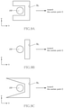
- FIGS. 9A to 9C are plan views illustrating variations of the slit SL.
- the slit SL of FIG. 9A has a shape in which a portion extending in the x-direction and a portion extending in the y-direction are each formed linearly to thereby linearly surround the feed point FP in three directions.
- the slit SL surrounding the feed point FP may not necessarily have a rounded shape but may have a linear shape.
- the slit SL of FIG. 9B is constituted of only a portion positioned between the feed point FP and the center point C and extending in the y-direction. As illustrated in FIG. 9B , the slit SL may not necessarily surround the feed point FP.
- the slit SL of FIG. 9A has a shape in which a portion extending in the x-direction and a portion extending in the y-direction are each formed linearly to thereby linearly surround the feed point FP in three directions.
- the slit SL surrounding the feed point FP may not necessarily have a rounded shape but may have
- 9C has a shape in which the width of a portion extending in the x-direction is reduced with the increasing distance from the center point C. This gradually increases the width of the conductor from the feed point FP toward the outer peripheral end of the patch conductor PA 1 .
- the slit SL in such a shape, the flow of current on the patch conductor PA 1 becomes smoother.
- FIG. 10 is a schematic perspective view for explaining the configuration of an antenna module 100 A in which a plurality of antenna modules 100 are laid out in an array.
- nine antenna modules 100 are laid out in an array on the xy plane.
- a so-called phased array can be achieved.
- the direction of beam can be changed as desired.
Landscapes
- Physics & Mathematics (AREA)
- Electromagnetism (AREA)
- Engineering & Computer Science (AREA)
- Microelectronics & Electronic Packaging (AREA)
- Waveguide Aerials (AREA)
- Aerials With Secondary Devices (AREA)
- Variable-Direction Aerials And Aerial Arrays (AREA)
Applications Claiming Priority (3)
| Application Number | Priority Date | Filing Date | Title |
|---|---|---|---|
| JP2017-207900 | 2017-10-27 | ||
| JP2017207900A JP6705435B2 (ja) | 2017-10-27 | 2017-10-27 | パッチアンテナ及びこれを備えるアンテナモジュール |
| JPJP2017-207900 | 2017-10-27 |
Publications (2)
| Publication Number | Publication Date |
|---|---|
| US20190131711A1 US20190131711A1 (en) | 2019-05-02 |
| US11228110B2 true US11228110B2 (en) | 2022-01-18 |
Family
ID=66244314
Family Applications (1)
| Application Number | Title | Priority Date | Filing Date |
|---|---|---|---|
| US16/173,218 Active US11228110B2 (en) | 2017-10-27 | 2018-10-29 | Patch antenna and antenna module having the same |
Country Status (3)
| Country | Link |
|---|---|
| US (1) | US11228110B2 (ja) |
| JP (1) | JP6705435B2 (ja) |
| CN (1) | CN109728423B (ja) |
Families Citing this family (2)
| Publication number | Priority date | Publication date | Assignee | Title |
|---|---|---|---|---|
| CN109742525B (zh) * | 2018-12-31 | 2021-02-23 | 瑞声科技(南京)有限公司 | 一种滤波天线 |
| CN112751168B (zh) * | 2019-10-31 | 2022-11-08 | Oppo广东移动通信有限公司 | 天线模组及电子设备 |
Citations (25)
| Publication number | Priority date | Publication date | Assignee | Title |
|---|---|---|---|---|
| US3978488A (en) * | 1975-04-24 | 1976-08-31 | The United States Of America As Represented By The Secretary Of The Navy | Offset fed electric microstrip dipole antenna |
| US4771291A (en) * | 1985-08-30 | 1988-09-13 | The United States Of America As Represented By The Secretary Of The Air Force | Dual frequency microstrip antenna |
| US5099249A (en) * | 1987-10-13 | 1992-03-24 | Seavey Engineering Associates, Inc. | Microstrip antenna for vehicular satellite communications |
| US5400041A (en) * | 1991-07-26 | 1995-03-21 | Strickland; Peter C. | Radiating element incorporating impedance transformation capabilities |
| US6014105A (en) * | 1999-01-19 | 2000-01-11 | The United States Of America As Represented By The Secretary Of The Navy | Microstrip antenna having an internal feed |
| US6195048B1 (en) * | 1997-12-01 | 2001-02-27 | Kabushiki Kaisha Toshiba | Multifrequency inverted F-type antenna |
| US6774853B2 (en) * | 2002-11-07 | 2004-08-10 | Accton Technology Corporation | Dual-band planar monopole antenna with a U-shaped slot |
| US20050243005A1 (en) * | 2004-04-27 | 2005-11-03 | Gholamreza Rafi | Low profile hybrid phased array antenna system configuration and element |
| JP2005348345A (ja) | 2004-06-07 | 2005-12-15 | Alps Electric Co Ltd | パッチアンテナ |
| US7038631B2 (en) * | 2001-06-18 | 2006-05-02 | Centre National De Le Recherche Scientifique (Cnrs) | Multi-frequency wire-plate antenna |
| US7221321B2 (en) * | 2004-11-17 | 2007-05-22 | Jasco Trading (Proprietary) Limited | Dual-frequency dual polarization antenna |
| US20080316110A1 (en) * | 2007-06-22 | 2008-12-25 | Suncall Corporation | Patch Antenna and RFID Inlet |
| US20090153404A1 (en) * | 2005-12-16 | 2009-06-18 | E.M.W. Antenna Co., Ltd. | Single layer dual band antenna with circular polarization and single feed point |
| US20100253583A1 (en) * | 2008-01-07 | 2010-10-07 | Fujitsu Limited | Electronic device, antenna and article |
| US20110012788A1 (en) * | 2009-07-14 | 2011-01-20 | Hong Kong Applied Science And Technology Research Institute Co., Ltd. | Miniature Circularly Polarized Folded Patch Antenna |
| JP2013150112A (ja) | 2012-01-18 | 2013-08-01 | Mitsumi Electric Co Ltd | アンテナモジュールおよびその特性調整方法 |
| US20140210674A1 (en) * | 2011-08-26 | 2014-07-31 | Yoshiyuki Yonei | Planar inverted f antenna |
| US20150084208A1 (en) * | 2013-09-25 | 2015-03-26 | Kabushiki Kaisha Toshiba | Connection member, semiconductor device, and stacked structure |
| US20150303576A1 (en) * | 2012-11-21 | 2015-10-22 | Eseo | Miniaturized Patch Antenna |
| US20160079676A1 (en) * | 2014-09-12 | 2016-03-17 | Taoglas Group Holdings Limited | Wifi patch antenna with dual u-shaped slots |
| US20160190868A1 (en) * | 2014-12-29 | 2016-06-30 | Shuai SHAO | Individual antenna element |
| US20160308402A1 (en) * | 2015-04-20 | 2016-10-20 | Babak Alavikia | Electromagnetic Energy Harvesting Using Complementary Split-Ring Resonators |
| EP3200278A1 (en) | 2014-09-25 | 2017-08-02 | Nec Corporation | Antenna system |
| JP2017191961A (ja) | 2016-04-11 | 2017-10-19 | 三菱電機株式会社 | アンテナ装置 |
| US20180337148A1 (en) * | 2017-05-19 | 2018-11-22 | Samsung Electro-Mechanics Co., Ltd. | Composite antenna substrate and semiconductor package module |
Family Cites Families (6)
| Publication number | Priority date | Publication date | Assignee | Title |
|---|---|---|---|---|
| TW431030B (en) * | 1999-10-22 | 2001-04-21 | Weng Jin Lu | A broadband rectangular patch antenna with a pair of wide slits |
| CN101080849B (zh) * | 2004-12-14 | 2012-07-25 | 富士通株式会社 | 天线 |
| JP5737048B2 (ja) * | 2011-08-12 | 2015-06-17 | カシオ計算機株式会社 | パッチアンテナ装置及び電波受信機器 |
| CN203039102U (zh) * | 2013-01-15 | 2013-07-03 | 厦门松元电子有限公司 | 一种变大阻抗的圆极化陶瓷天线 |
| CN104868243A (zh) * | 2015-05-28 | 2015-08-26 | 电子科技大学 | 一种工作模式可切换的双频段可穿戴天线 |
| CN205039246U (zh) * | 2015-09-29 | 2016-02-17 | 辽宁普天数码股份有限公司 | 一种基于e型贴片的数字电视发射天线 |
-
2017
- 2017-10-27 JP JP2017207900A patent/JP6705435B2/ja active Active
-
2018
- 2018-10-26 CN CN201811257974.2A patent/CN109728423B/zh active Active
- 2018-10-29 US US16/173,218 patent/US11228110B2/en active Active
Patent Citations (26)
| Publication number | Priority date | Publication date | Assignee | Title |
|---|---|---|---|---|
| US3978488A (en) * | 1975-04-24 | 1976-08-31 | The United States Of America As Represented By The Secretary Of The Navy | Offset fed electric microstrip dipole antenna |
| US4771291A (en) * | 1985-08-30 | 1988-09-13 | The United States Of America As Represented By The Secretary Of The Air Force | Dual frequency microstrip antenna |
| US5099249A (en) * | 1987-10-13 | 1992-03-24 | Seavey Engineering Associates, Inc. | Microstrip antenna for vehicular satellite communications |
| US5400041A (en) * | 1991-07-26 | 1995-03-21 | Strickland; Peter C. | Radiating element incorporating impedance transformation capabilities |
| US6195048B1 (en) * | 1997-12-01 | 2001-02-27 | Kabushiki Kaisha Toshiba | Multifrequency inverted F-type antenna |
| US6014105A (en) * | 1999-01-19 | 2000-01-11 | The United States Of America As Represented By The Secretary Of The Navy | Microstrip antenna having an internal feed |
| US7038631B2 (en) * | 2001-06-18 | 2006-05-02 | Centre National De Le Recherche Scientifique (Cnrs) | Multi-frequency wire-plate antenna |
| US6774853B2 (en) * | 2002-11-07 | 2004-08-10 | Accton Technology Corporation | Dual-band planar monopole antenna with a U-shaped slot |
| US20050243005A1 (en) * | 2004-04-27 | 2005-11-03 | Gholamreza Rafi | Low profile hybrid phased array antenna system configuration and element |
| US7161537B2 (en) * | 2004-04-27 | 2007-01-09 | Intelwaves Technologies Ltd. | Low profile hybrid phased array antenna system configuration and element |
| JP2005348345A (ja) | 2004-06-07 | 2005-12-15 | Alps Electric Co Ltd | パッチアンテナ |
| US7221321B2 (en) * | 2004-11-17 | 2007-05-22 | Jasco Trading (Proprietary) Limited | Dual-frequency dual polarization antenna |
| US20090153404A1 (en) * | 2005-12-16 | 2009-06-18 | E.M.W. Antenna Co., Ltd. | Single layer dual band antenna with circular polarization and single feed point |
| US20080316110A1 (en) * | 2007-06-22 | 2008-12-25 | Suncall Corporation | Patch Antenna and RFID Inlet |
| US20100253583A1 (en) * | 2008-01-07 | 2010-10-07 | Fujitsu Limited | Electronic device, antenna and article |
| US20110012788A1 (en) * | 2009-07-14 | 2011-01-20 | Hong Kong Applied Science And Technology Research Institute Co., Ltd. | Miniature Circularly Polarized Folded Patch Antenna |
| US20140210674A1 (en) * | 2011-08-26 | 2014-07-31 | Yoshiyuki Yonei | Planar inverted f antenna |
| JP2013150112A (ja) | 2012-01-18 | 2013-08-01 | Mitsumi Electric Co Ltd | アンテナモジュールおよびその特性調整方法 |
| US20150303576A1 (en) * | 2012-11-21 | 2015-10-22 | Eseo | Miniaturized Patch Antenna |
| US20150084208A1 (en) * | 2013-09-25 | 2015-03-26 | Kabushiki Kaisha Toshiba | Connection member, semiconductor device, and stacked structure |
| US20160079676A1 (en) * | 2014-09-12 | 2016-03-17 | Taoglas Group Holdings Limited | Wifi patch antenna with dual u-shaped slots |
| EP3200278A1 (en) | 2014-09-25 | 2017-08-02 | Nec Corporation | Antenna system |
| US20160190868A1 (en) * | 2014-12-29 | 2016-06-30 | Shuai SHAO | Individual antenna element |
| US20160308402A1 (en) * | 2015-04-20 | 2016-10-20 | Babak Alavikia | Electromagnetic Energy Harvesting Using Complementary Split-Ring Resonators |
| JP2017191961A (ja) | 2016-04-11 | 2017-10-19 | 三菱電機株式会社 | アンテナ装置 |
| US20180337148A1 (en) * | 2017-05-19 | 2018-11-22 | Samsung Electro-Mechanics Co., Ltd. | Composite antenna substrate and semiconductor package module |
Also Published As
| Publication number | Publication date |
|---|---|
| CN109728423B (zh) | 2022-03-01 |
| JP2019080277A (ja) | 2019-05-23 |
| US20190131711A1 (en) | 2019-05-02 |
| CN109728423A (zh) | 2019-05-07 |
| JP6705435B2 (ja) | 2020-06-03 |
Similar Documents
| Publication | Publication Date | Title |
|---|---|---|
| JP6930591B2 (ja) | アンテナモジュールおよび通信装置 | |
| US10854950B2 (en) | Antenna device | |
| WO2013027824A1 (ja) | アンテナ及び電子装置 | |
| JP6915745B2 (ja) | アンテナモジュールおよびそれを搭載した通信装置 | |
| CN111200184B (zh) | 天线模块 | |
| US20210119337A1 (en) | Antenna device | |
| US11228110B2 (en) | Patch antenna and antenna module having the same | |
| JP2018050207A (ja) | アンテナ装置 | |
| WO2013099286A1 (ja) | 多層配線基板 | |
| JP5675934B1 (ja) | アンテナ装置 | |
| JP6690672B2 (ja) | パッチアンテナ及びこれを備えるアンテナモジュール | |
| JP6533560B2 (ja) | アンテナ装置 | |
| US20140043190A1 (en) | Planar inverted f antenna structure | |
| KR20150011711A (ko) | 이중 급전방식의 광대역 패치안테나 및 그 제조방법 | |
| JP4148941B2 (ja) | 複合アンテナ | |
| JP5737095B2 (ja) | アンテナ装置 | |
| JP6589815B2 (ja) | アンテナ装置 | |
| JP6909766B2 (ja) | アンテナ装置 | |
| KR102600023B1 (ko) | 안테나 장치 | |
| WO2017068885A1 (ja) | アンテナ装置 | |
| US11757192B2 (en) | Antenna device with patch including a slit | |
| JP2011015329A (ja) | 統合アンテナ | |
| WO2021100655A1 (ja) | 平面アンテナ | |
| JP7156815B2 (ja) | アンテナ及び半導体装置 | |
| JP2018182362A (ja) | アンテナ装置 |
Legal Events
| Date | Code | Title | Description |
|---|---|---|---|
| AS | Assignment |
Owner name: TDK CORPORATION, JAPAN Free format text: ASSIGNMENT OF ASSIGNORS INTEREST;ASSIGNOR:SOTOMA, NAOKI;REEL/FRAME:047338/0723 Effective date: 20181012 |
|
| FEPP | Fee payment procedure |
Free format text: ENTITY STATUS SET TO UNDISCOUNTED (ORIGINAL EVENT CODE: BIG.); ENTITY STATUS OF PATENT OWNER: LARGE ENTITY |
|
| STPP | Information on status: patent application and granting procedure in general |
Free format text: DOCKETED NEW CASE - READY FOR EXAMINATION |
|
| STPP | Information on status: patent application and granting procedure in general |
Free format text: NON FINAL ACTION MAILED |
|
| STPP | Information on status: patent application and granting procedure in general |
Free format text: FINAL REJECTION MAILED |
|
| STPP | Information on status: patent application and granting procedure in general |
Free format text: DOCKETED NEW CASE - READY FOR EXAMINATION |
|
| STPP | Information on status: patent application and granting procedure in general |
Free format text: NON FINAL ACTION MAILED |
|
| STPP | Information on status: patent application and granting procedure in general |
Free format text: RESPONSE TO NON-FINAL OFFICE ACTION ENTERED AND FORWARDED TO EXAMINER |
|
| STPP | Information on status: patent application and granting procedure in general |
Free format text: FINAL REJECTION MAILED |
|
| STPP | Information on status: patent application and granting procedure in general |
Free format text: NOTICE OF ALLOWANCE MAILED -- APPLICATION RECEIVED IN OFFICE OF PUBLICATIONS |
|
| STPP | Information on status: patent application and granting procedure in general |
Free format text: PUBLICATIONS -- ISSUE FEE PAYMENT VERIFIED |
|
| STCF | Information on status: patent grant |
Free format text: PATENTED CASE |