US10833210B2 - Solar cell and method for manufacturing the same - Google Patents
Solar cell and method for manufacturing the same Download PDFInfo
- Publication number
- US10833210B2 US10833210B2 US14/323,986 US201414323986A US10833210B2 US 10833210 B2 US10833210 B2 US 10833210B2 US 201414323986 A US201414323986 A US 201414323986A US 10833210 B2 US10833210 B2 US 10833210B2
- Authority
- US
- United States
- Prior art keywords
- conductive semiconductor
- layer
- semiconductor layer
- trench
- solar cell
- Prior art date
- Legal status (The legal status is an assumption and is not a legal conclusion. Google has not performed a legal analysis and makes no representation as to the accuracy of the status listed.)
- Active
Links
- 238000000034 method Methods 0.000 title description 34
- 238000004519 manufacturing process Methods 0.000 title description 20
- 239000004065 semiconductor Substances 0.000 claims abstract description 379
- 239000000758 substrate Substances 0.000 claims abstract description 97
- 230000005641 tunneling Effects 0.000 claims abstract description 73
- 238000000926 separation method Methods 0.000 claims abstract description 39
- 238000009413 insulation Methods 0.000 claims description 35
- WYTGDNHDOZPMIW-RCBQFDQVSA-N alstonine Natural products C1=CC2=C3C=CC=CC3=NC2=C2N1C[C@H]1[C@H](C)OC=C(C(=O)OC)[C@H]1C2 WYTGDNHDOZPMIW-RCBQFDQVSA-N 0.000 claims description 2
- 229910021421 monocrystalline silicon Inorganic materials 0.000 claims description 2
- 238000009751 slip forming Methods 0.000 claims 1
- 239000010410 layer Substances 0.000 description 456
- 239000002019 doping agent Substances 0.000 description 50
- WGTYBPLFGIVFAS-UHFFFAOYSA-M tetramethylammonium hydroxide Chemical compound [OH-].C[N+](C)(C)C WGTYBPLFGIVFAS-UHFFFAOYSA-M 0.000 description 28
- 238000002161 passivation Methods 0.000 description 26
- XUIMIQQOPSSXEZ-UHFFFAOYSA-N Silicon Chemical compound [Si] XUIMIQQOPSSXEZ-UHFFFAOYSA-N 0.000 description 16
- 229910052710 silicon Inorganic materials 0.000 description 16
- 239000010703 silicon Substances 0.000 description 16
- 238000005530 etching Methods 0.000 description 14
- 239000000463 material Substances 0.000 description 14
- 229910052814 silicon oxide Inorganic materials 0.000 description 11
- VYPSYNLAJGMNEJ-UHFFFAOYSA-N Silicium dioxide Chemical compound O=[Si]=O VYPSYNLAJGMNEJ-UHFFFAOYSA-N 0.000 description 9
- 230000015572 biosynthetic process Effects 0.000 description 8
- 230000004075 alteration Effects 0.000 description 7
- 230000000694 effects Effects 0.000 description 7
- BHEPBYXIRTUNPN-UHFFFAOYSA-N hydridophosphorus(.) (triplet) Chemical compound [PH] BHEPBYXIRTUNPN-UHFFFAOYSA-N 0.000 description 7
- ZOXJGFHDIHLPTG-UHFFFAOYSA-N Boron Chemical compound [B] ZOXJGFHDIHLPTG-UHFFFAOYSA-N 0.000 description 6
- 229910052796 boron Inorganic materials 0.000 description 6
- 239000013078 crystal Substances 0.000 description 6
- 239000005368 silicate glass Substances 0.000 description 6
- 239000000969 carrier Substances 0.000 description 5
- 238000007650 screen-printing Methods 0.000 description 5
- 229910052581 Si3N4 Inorganic materials 0.000 description 4
- GWEVSGVZZGPLCZ-UHFFFAOYSA-N Titan oxide Chemical compound O=[Ti]=O GWEVSGVZZGPLCZ-UHFFFAOYSA-N 0.000 description 4
- 229910052787 antimony Inorganic materials 0.000 description 4
- WATWJIUSRGPENY-UHFFFAOYSA-N antimony atom Chemical compound [Sb] WATWJIUSRGPENY-UHFFFAOYSA-N 0.000 description 4
- 229910052785 arsenic Inorganic materials 0.000 description 4
- RQNWIZPPADIBDY-UHFFFAOYSA-N arsenic atom Chemical compound [As] RQNWIZPPADIBDY-UHFFFAOYSA-N 0.000 description 4
- 229910052797 bismuth Inorganic materials 0.000 description 4
- JCXGWMGPZLAOME-UHFFFAOYSA-N bismuth atom Chemical compound [Bi] JCXGWMGPZLAOME-UHFFFAOYSA-N 0.000 description 4
- 229910021478 group 5 element Inorganic materials 0.000 description 4
- 230000006798 recombination Effects 0.000 description 4
- 238000005215 recombination Methods 0.000 description 4
- HQVNEWCFYHHQES-UHFFFAOYSA-N silicon nitride Chemical compound N12[Si]34N5[Si]62N3[Si]51N64 HQVNEWCFYHHQES-UHFFFAOYSA-N 0.000 description 4
- 125000006850 spacer group Chemical group 0.000 description 4
- GYHNNYVSQQEPJS-UHFFFAOYSA-N Gallium Chemical compound [Ga] GYHNNYVSQQEPJS-UHFFFAOYSA-N 0.000 description 3
- 229910052782 aluminium Inorganic materials 0.000 description 3
- XAGFODPZIPBFFR-UHFFFAOYSA-N aluminium Chemical compound [Al] XAGFODPZIPBFFR-UHFFFAOYSA-N 0.000 description 3
- 230000008901 benefit Effects 0.000 description 3
- 238000006243 chemical reaction Methods 0.000 description 3
- 238000000151 deposition Methods 0.000 description 3
- 230000008021 deposition Effects 0.000 description 3
- 230000005684 electric field Effects 0.000 description 3
- 229910052733 gallium Inorganic materials 0.000 description 3
- 229910052738 indium Inorganic materials 0.000 description 3
- APFVFJFRJDLVQX-UHFFFAOYSA-N indium atom Chemical compound [In] APFVFJFRJDLVQX-UHFFFAOYSA-N 0.000 description 3
- 238000000059 patterning Methods 0.000 description 3
- 239000002356 single layer Substances 0.000 description 3
- 230000003746 surface roughness Effects 0.000 description 3
- 238000007669 thermal treatment Methods 0.000 description 3
- 239000002253 acid Substances 0.000 description 2
- 229910021417 amorphous silicon Inorganic materials 0.000 description 2
- 238000000231 atomic layer deposition Methods 0.000 description 2
- CETPSERCERDGAM-UHFFFAOYSA-N ceric oxide Chemical compound O=[Ce]=O CETPSERCERDGAM-UHFFFAOYSA-N 0.000 description 2
- 229910000422 cerium(IV) oxide Inorganic materials 0.000 description 2
- 238000005229 chemical vapour deposition Methods 0.000 description 2
- 229910052739 hydrogen Inorganic materials 0.000 description 2
- 239000001257 hydrogen Substances 0.000 description 2
- 125000004435 hydrogen atom Chemical class [H]* 0.000 description 2
- 238000007641 inkjet printing Methods 0.000 description 2
- 238000000608 laser ablation Methods 0.000 description 2
- 229910001635 magnesium fluoride Inorganic materials 0.000 description 2
- 150000004767 nitrides Chemical class 0.000 description 2
- 238000001020 plasma etching Methods 0.000 description 2
- 238000000623 plasma-assisted chemical vapour deposition Methods 0.000 description 2
- 238000005498 polishing Methods 0.000 description 2
- -1 silicon oxide nitride Chemical class 0.000 description 2
- 229910052950 sphalerite Inorganic materials 0.000 description 2
- 238000004528 spin coating Methods 0.000 description 2
- 238000005507 spraying Methods 0.000 description 2
- 238000001771 vacuum deposition Methods 0.000 description 2
- XLYOFNOQVPJJNP-UHFFFAOYSA-N water Substances O XLYOFNOQVPJJNP-UHFFFAOYSA-N 0.000 description 2
- 229910052984 zinc sulfide Inorganic materials 0.000 description 2
- BPQQTUXANYXVAA-UHFFFAOYSA-N Orthosilicate Chemical compound [O-][Si]([O-])([O-])[O-] BPQQTUXANYXVAA-UHFFFAOYSA-N 0.000 description 1
- PNEYBMLMFCGWSK-UHFFFAOYSA-N aluminium oxide Inorganic materials [O-2].[O-2].[O-2].[Al+3].[Al+3] PNEYBMLMFCGWSK-UHFFFAOYSA-N 0.000 description 1
- 238000005452 bending Methods 0.000 description 1
- 239000003245 coal Substances 0.000 description 1
- 229920001940 conductive polymer Polymers 0.000 description 1
- 239000000470 constituent Substances 0.000 description 1
- 230000001276 controlling effect Effects 0.000 description 1
- 229910052593 corundum Inorganic materials 0.000 description 1
- 238000005520 cutting process Methods 0.000 description 1
- 230000007547 defect Effects 0.000 description 1
- 229910003460 diamond Inorganic materials 0.000 description 1
- 239000010432 diamond Substances 0.000 description 1
- 238000007598 dipping method Methods 0.000 description 1
- 238000010292 electrical insulation Methods 0.000 description 1
- 238000010304 firing Methods 0.000 description 1
- 239000012774 insulation material Substances 0.000 description 1
- 238000005468 ion implantation Methods 0.000 description 1
- 230000007774 longterm Effects 0.000 description 1
- 229910052751 metal Inorganic materials 0.000 description 1
- 239000002184 metal Substances 0.000 description 1
- 150000002739 metals Chemical class 0.000 description 1
- 238000012986 modification Methods 0.000 description 1
- 230000004048 modification Effects 0.000 description 1
- 239000003921 oil Substances 0.000 description 1
- 238000000206 photolithography Methods 0.000 description 1
- 238000007747 plating Methods 0.000 description 1
- 238000007517 polishing process Methods 0.000 description 1
- 230000001105 regulatory effect Effects 0.000 description 1
- 229910001845 yogo sapphire Inorganic materials 0.000 description 1
Images


Classifications
-
- H—ELECTRICITY
- H01—ELECTRIC ELEMENTS
- H01L—SEMICONDUCTOR DEVICES NOT COVERED BY CLASS H10
- H01L31/00—Semiconductor devices sensitive to infrared radiation, light, electromagnetic radiation of shorter wavelength or corpuscular radiation and specially adapted either for the conversion of the energy of such radiation into electrical energy or for the control of electrical energy by such radiation; Processes or apparatus specially adapted for the manufacture or treatment thereof or of parts thereof; Details thereof
- H01L31/04—Semiconductor devices sensitive to infrared radiation, light, electromagnetic radiation of shorter wavelength or corpuscular radiation and specially adapted either for the conversion of the energy of such radiation into electrical energy or for the control of electrical energy by such radiation; Processes or apparatus specially adapted for the manufacture or treatment thereof or of parts thereof; Details thereof adapted as photovoltaic [PV] conversion devices
-
- H—ELECTRICITY
- H01—ELECTRIC ELEMENTS
- H01L—SEMICONDUCTOR DEVICES NOT COVERED BY CLASS H10
- H01L31/00—Semiconductor devices sensitive to infrared radiation, light, electromagnetic radiation of shorter wavelength or corpuscular radiation and specially adapted either for the conversion of the energy of such radiation into electrical energy or for the control of electrical energy by such radiation; Processes or apparatus specially adapted for the manufacture or treatment thereof or of parts thereof; Details thereof
- H01L31/02—Details
- H01L31/0224—Electrodes
- H01L31/022408—Electrodes for devices characterised by at least one potential jump barrier or surface barrier
- H01L31/022425—Electrodes for devices characterised by at least one potential jump barrier or surface barrier for solar cells
- H01L31/022441—Electrode arrangements specially adapted for back-contact solar cells
-
- H—ELECTRICITY
- H01—ELECTRIC ELEMENTS
- H01L—SEMICONDUCTOR DEVICES NOT COVERED BY CLASS H10
- H01L31/00—Semiconductor devices sensitive to infrared radiation, light, electromagnetic radiation of shorter wavelength or corpuscular radiation and specially adapted either for the conversion of the energy of such radiation into electrical energy or for the control of electrical energy by such radiation; Processes or apparatus specially adapted for the manufacture or treatment thereof or of parts thereof; Details thereof
- H01L31/02—Details
- H01L31/0216—Coatings
-
- H—ELECTRICITY
- H01—ELECTRIC ELEMENTS
- H01L—SEMICONDUCTOR DEVICES NOT COVERED BY CLASS H10
- H01L31/00—Semiconductor devices sensitive to infrared radiation, light, electromagnetic radiation of shorter wavelength or corpuscular radiation and specially adapted either for the conversion of the energy of such radiation into electrical energy or for the control of electrical energy by such radiation; Processes or apparatus specially adapted for the manufacture or treatment thereof or of parts thereof; Details thereof
- H01L31/0248—Semiconductor devices sensitive to infrared radiation, light, electromagnetic radiation of shorter wavelength or corpuscular radiation and specially adapted either for the conversion of the energy of such radiation into electrical energy or for the control of electrical energy by such radiation; Processes or apparatus specially adapted for the manufacture or treatment thereof or of parts thereof; Details thereof characterised by their semiconductor bodies
- H01L31/0256—Semiconductor devices sensitive to infrared radiation, light, electromagnetic radiation of shorter wavelength or corpuscular radiation and specially adapted either for the conversion of the energy of such radiation into electrical energy or for the control of electrical energy by such radiation; Processes or apparatus specially adapted for the manufacture or treatment thereof or of parts thereof; Details thereof characterised by their semiconductor bodies characterised by the material
- H01L31/0264—Inorganic materials
- H01L31/028—Inorganic materials including, apart from doping material or other impurities, only elements of Group IV of the Periodic System
-
- H—ELECTRICITY
- H01—ELECTRIC ELEMENTS
- H01L—SEMICONDUCTOR DEVICES NOT COVERED BY CLASS H10
- H01L31/00—Semiconductor devices sensitive to infrared radiation, light, electromagnetic radiation of shorter wavelength or corpuscular radiation and specially adapted either for the conversion of the energy of such radiation into electrical energy or for the control of electrical energy by such radiation; Processes or apparatus specially adapted for the manufacture or treatment thereof or of parts thereof; Details thereof
- H01L31/04—Semiconductor devices sensitive to infrared radiation, light, electromagnetic radiation of shorter wavelength or corpuscular radiation and specially adapted either for the conversion of the energy of such radiation into electrical energy or for the control of electrical energy by such radiation; Processes or apparatus specially adapted for the manufacture or treatment thereof or of parts thereof; Details thereof adapted as photovoltaic [PV] conversion devices
- H01L31/06—Semiconductor devices sensitive to infrared radiation, light, electromagnetic radiation of shorter wavelength or corpuscular radiation and specially adapted either for the conversion of the energy of such radiation into electrical energy or for the control of electrical energy by such radiation; Processes or apparatus specially adapted for the manufacture or treatment thereof or of parts thereof; Details thereof adapted as photovoltaic [PV] conversion devices characterised by at least one potential-jump barrier or surface barrier
- H01L31/068—Semiconductor devices sensitive to infrared radiation, light, electromagnetic radiation of shorter wavelength or corpuscular radiation and specially adapted either for the conversion of the energy of such radiation into electrical energy or for the control of electrical energy by such radiation; Processes or apparatus specially adapted for the manufacture or treatment thereof or of parts thereof; Details thereof adapted as photovoltaic [PV] conversion devices characterised by at least one potential-jump barrier or surface barrier the potential barriers being only of the PN homojunction type, e.g. bulk silicon PN homojunction solar cells or thin film polycrystalline silicon PN homojunction solar cells
- H01L31/0682—Semiconductor devices sensitive to infrared radiation, light, electromagnetic radiation of shorter wavelength or corpuscular radiation and specially adapted either for the conversion of the energy of such radiation into electrical energy or for the control of electrical energy by such radiation; Processes or apparatus specially adapted for the manufacture or treatment thereof or of parts thereof; Details thereof adapted as photovoltaic [PV] conversion devices characterised by at least one potential-jump barrier or surface barrier the potential barriers being only of the PN homojunction type, e.g. bulk silicon PN homojunction solar cells or thin film polycrystalline silicon PN homojunction solar cells back-junction, i.e. rearside emitter, solar cells, e.g. interdigitated base-emitter regions back-junction cells
-
- H—ELECTRICITY
- H01—ELECTRIC ELEMENTS
- H01L—SEMICONDUCTOR DEVICES NOT COVERED BY CLASS H10
- H01L31/00—Semiconductor devices sensitive to infrared radiation, light, electromagnetic radiation of shorter wavelength or corpuscular radiation and specially adapted either for the conversion of the energy of such radiation into electrical energy or for the control of electrical energy by such radiation; Processes or apparatus specially adapted for the manufacture or treatment thereof or of parts thereof; Details thereof
- H01L31/18—Processes or apparatus specially adapted for the manufacture or treatment of these devices or of parts thereof
- H01L31/1804—Processes or apparatus specially adapted for the manufacture or treatment of these devices or of parts thereof comprising only elements of Group IV of the Periodic System
- H01L31/182—Special manufacturing methods for polycrystalline Si, e.g. Si ribbon, poly Si ingots, thin films of polycrystalline Si
- H01L31/1824—Special manufacturing methods for microcrystalline Si, uc-Si
-
- Y—GENERAL TAGGING OF NEW TECHNOLOGICAL DEVELOPMENTS; GENERAL TAGGING OF CROSS-SECTIONAL TECHNOLOGIES SPANNING OVER SEVERAL SECTIONS OF THE IPC; TECHNICAL SUBJECTS COVERED BY FORMER USPC CROSS-REFERENCE ART COLLECTIONS [XRACs] AND DIGESTS
- Y02—TECHNOLOGIES OR APPLICATIONS FOR MITIGATION OR ADAPTATION AGAINST CLIMATE CHANGE
- Y02E—REDUCTION OF GREENHOUSE GAS [GHG] EMISSIONS, RELATED TO ENERGY GENERATION, TRANSMISSION OR DISTRIBUTION
- Y02E10/00—Energy generation through renewable energy sources
- Y02E10/50—Photovoltaic [PV] energy
- Y02E10/545—Microcrystalline silicon PV cells
-
- Y—GENERAL TAGGING OF NEW TECHNOLOGICAL DEVELOPMENTS; GENERAL TAGGING OF CROSS-SECTIONAL TECHNOLOGIES SPANNING OVER SEVERAL SECTIONS OF THE IPC; TECHNICAL SUBJECTS COVERED BY FORMER USPC CROSS-REFERENCE ART COLLECTIONS [XRACs] AND DIGESTS
- Y02—TECHNOLOGIES OR APPLICATIONS FOR MITIGATION OR ADAPTATION AGAINST CLIMATE CHANGE
- Y02E—REDUCTION OF GREENHOUSE GAS [GHG] EMISSIONS, RELATED TO ENERGY GENERATION, TRANSMISSION OR DISTRIBUTION
- Y02E10/00—Energy generation through renewable energy sources
- Y02E10/50—Photovoltaic [PV] energy
- Y02E10/546—Polycrystalline silicon PV cells
-
- Y—GENERAL TAGGING OF NEW TECHNOLOGICAL DEVELOPMENTS; GENERAL TAGGING OF CROSS-SECTIONAL TECHNOLOGIES SPANNING OVER SEVERAL SECTIONS OF THE IPC; TECHNICAL SUBJECTS COVERED BY FORMER USPC CROSS-REFERENCE ART COLLECTIONS [XRACs] AND DIGESTS
- Y02—TECHNOLOGIES OR APPLICATIONS FOR MITIGATION OR ADAPTATION AGAINST CLIMATE CHANGE
- Y02E—REDUCTION OF GREENHOUSE GAS [GHG] EMISSIONS, RELATED TO ENERGY GENERATION, TRANSMISSION OR DISTRIBUTION
- Y02E10/00—Energy generation through renewable energy sources
- Y02E10/50—Photovoltaic [PV] energy
- Y02E10/547—Monocrystalline silicon PV cells
-
- Y—GENERAL TAGGING OF NEW TECHNOLOGICAL DEVELOPMENTS; GENERAL TAGGING OF CROSS-SECTIONAL TECHNOLOGIES SPANNING OVER SEVERAL SECTIONS OF THE IPC; TECHNICAL SUBJECTS COVERED BY FORMER USPC CROSS-REFERENCE ART COLLECTIONS [XRACs] AND DIGESTS
- Y02—TECHNOLOGIES OR APPLICATIONS FOR MITIGATION OR ADAPTATION AGAINST CLIMATE CHANGE
- Y02P—CLIMATE CHANGE MITIGATION TECHNOLOGIES IN THE PRODUCTION OR PROCESSING OF GOODS
- Y02P70/00—Climate change mitigation technologies in the production process for final industrial or consumer products
- Y02P70/50—Manufacturing or production processes characterised by the final manufactured product
-
- Y02P70/521—
Definitions
- Embodiments of the invention relate to a solar cell and a method for manufacturing the same and, more particularly, to a solar cell having a back surface electrode structure and a method for manufacturing the same.
- Solar cells may be fabricated via formation of various layers and electrodes based on designs.
- the designs of various layers and electrodes may determine the efficiency of solar cells.
- the most important requirement for commercialization of solar cells is to overcome the low efficiency of solar cells and to design various layers and electrodes so as to maximize the efficiency of solar cells.
- the embodiments of the invention have been made in view of the above issues, and it is an object of the embodiments of the invention to provide a solar cell having excellent properties and high productivity and a method for manufacturing the same.
- a solar cell including a semiconductor substrate, a tunneling layer formed on one surface of the semiconductor substrate, a first conductive semiconductor layer formed on a surface of the tunneling layer, a second conductive semiconductor layer formed on the surface of the tunneling layer, and a separation portion to separate the first and second conductive semiconductor layers from each other, and is formed on the surface of the tunneling layer at a location corresponding to at least a portion of a boundary between the first and second conductive semiconductor layers.
- a method for manufacturing a solar cell including forming a tunneling layer on one surface of a semiconductor substrate, forming a first conductive semiconductor layer and a second conductive semiconductor layer on a surface of the tunneling layer, the first and second conductive semiconductor layers coming into contact with each other and forming a trench in at least a portion of a boundary between the first and second conductive semiconductor layers by selectively removing portions of the first and second conductive semiconductor layers on the tunneling layer.
- a method for manufacturing a solar cell including preparing a semiconductor substrate, forming a tunneling layer on one surface of the semiconductor substrate, forming an intrinsic semiconductor layer on a surface of the tunneling layer and doping the intrinsic semiconductor layer with a first conductive dopant and a second conductive dopant to form a first conductive semiconductor layer and a second conductive semiconductor layer, respectively, wherein, in the doping, a boundary between the first conductive semiconductor layer and the second conductive semiconductor layer is partially undoped to form a separation portion.
- FIG. 1 is a sectional view showing a solar cell according to one embodiment of the invention.
- FIG. 2 is a rear plan view showing the solar cell according to the embodiment of the invention.
- FIGS. 3A to 3K are sectional views showing a method for manufacturing the solar cell according to the embodiment of the invention.
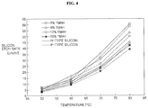
- FIG. 4 is a graph showing an etch rate of silicon using tetra-methyl ammonium hydroxide (TMAH) depending on temperature and density;
- TMAH tetra-methyl ammonium hydroxide
- FIG. 5 is a graph showing an etch rate of silicon oxide using tetra-methyl ammonium hydroxide depending on temperature and density;
- FIG. 6 is a rear plan view showing a solar cell according to another embodiment of the invention.
- FIG. 7 is a partial plan view showing first and second conductive semiconductor layers and a trench of the solar cell according to another embodiment of the invention.
- FIG. 8 is a sectional view showing a solar cell according to another embodiment of the invention.
- FIGS. 9A to 9F are sectional views showing a method for manufacturing the solar cell according to the embodiment of the invention.
- FIG. 10 is a sectional view showing a solar cell according to another embodiment of the invention.
- FIG. 11 is a sectional view showing a solar cell according to a further embodiment of the invention.
- FIG. 1 is a sectional view showing a solar cell according to one embodiment of the invention.
- the solar cell 100 includes a semiconductor substrate 10 , a tunneling layer 20 formed on one surface (e.g., a back surface) of the semiconductor substrate 10 , and a first conductive semiconductor layer and a second conductive semiconductor layer 34 which are formed on the tunneling layer 20 .
- the solar cell 100 may further include first and second electrodes 42 and 44 connected to the first and second conductive semiconductor layers 32 and 34 , the first and second electrodes 42 and serving to collect carriers.
- the solar cell 100 may further include a passivation film 60 , a front surface field layer 62 and an anti-reflection film 50 , for example. This will be described below in more detail.
- the semiconductor substrate 10 may include a base region 110 containing a first conductive dopant, the first conductive dopant being doped at a low density.
- the base region 110 may be formed of silicon containing the first conductive dopant.
- the silicon may be single-crystal silicon and the first conductive dopant may be an n-type dopant or a p-type dopant. That is, the first conductive dopant may be an n-type dopant including a group-V element, such as phosphorous (P), arsenic (As), bismuth (Bi), antimony (Sb) or the like.
- the first conductive dopant may be a p-type dopant including a group-III element, such as boron (B), aluminum (Al), gallium (Ga), indium (In) or the like.
- the semiconductor substrate 10 includes the base region 110 without an additional doping region. This may prevent damage to the semiconductor substrate 10 due to formation of the doping region and also prevent recombination in the doping region.
- the base region 110 may contain an n-type dopant as the first conductive dopant.
- the second conductive semiconductor layer 34 which forms tunnel junctions with the semiconductor substrate 10 (more particularly, the base region 110 ) through the tunneling layer 20 , may be a p-type layer.
- the second conductive semiconductor layer 34 may be formed over a wide area and serve as an emitter to cause photoelectric conversion by the junctions between the second conductive semiconductor layer 34 and the semiconductor substrate 10 , which may ensure effective collection of holes having less mobility than electrons.
- the embodiments of the invention are not limited thereto and the semiconductor substrate 10 and the first conductive semiconductor layer 32 may be a p-type and the second conductive semiconductor layer 34 may be an n-type.
- the front surface of the semiconductor substrate 10 may be subjected to texturing and, thus, have convex and concave portions (e.g., pyramidal portions or other shaped portions).
- the textured front surface of the semiconductor substrate 10 provided with the convex and concave portions, may attain increased surface roughness, which may reduce reflectance of light incident upon the front surface of the semiconductor substrate 10 . In this way, the quantity of light reaching the tunnel junctions formed by the semiconductor substrate 10 and the second conductive semiconductor layer 34 may be increased, which may minimize light loss.
- the back surface of the semiconductor substrate 10 may be subjected to polishing, for example, and may be a relatively smooth and flat surface having less surface roughness than the front surface of the semiconductor substrate 10 . As such, light having passed through the semiconductor substrate 10 to the back surface may be reflected by the back surface and then again progress into the semiconductor substrate 10 .
- properties of the solar cell 100 may be greatly changed according to properties of the back surface of the semiconductor substrate 10 . For this reason, the back surface of the semiconductor substrate 10 is not provided with convex and concave portions by texturing.
- the embodiments of the invention are not limited thereto and various alterations are possible.
- the passivation film 60 , the front surface field layer 62 and the anti-reflection film 50 may be formed on the front surface of the semiconductor substrate 10 (i.e. over the semiconductor substrate 10 ) in sequence.
- the passivation film 60 , the front surface field layer 62 and the anti-reflection film 50 may be formed on the entire front surface. This may maximize effects of the respective layers and simplify a manufacturing process thereof because patterning is unnecessary.
- the passivation film 60 basically serves to passivate defects present in the surface or bulk of the semiconductor substrate 10 .
- the front surface field layer 62 has a function similar to that of a Back Surface Field (BSF) layer because a first or second conductive dopant thereof has a greater density than that of the semiconductor substrate 10 . That is, the front surface field layer 62 creates an electric field to prevent recombination of carriers at the front surface of the semiconductor substrate 10 . This may increase an open-circuit voltage Voc of the solar cell 100 .
- the anti-reflection film 50 may serve to lower a reflectance of light incident upon the front surface of the semiconductor substrate 10 , thereby increasing the quantity of light reaching the tunnel junctions. This may increase a short-circuit current Isc of the solar cell 100 .
- the passivation film 60 and/or the anti-reflection film 50 may have a single-layer film structure of any one selected from the group consisting of a silicon nitride film, a silicon nitride film containing hydrogen, a silicon oxide film, a silicon oxide nitride film, MgF 2 , ZnS, TiO 2 , and CeO 2 , or a multi-layer film structure of at least two of the aforementioned material films.
- the passivation film 60 may be formed of an intrinsic amorphous semiconductor (for example, amorphous silicon), for example.
- the front surface field layer 62 may be formed of an amorphous semiconductor (for example, amorphous silicon) doped with a first or second conductive dopant.
- amorphous semiconductor for example, amorphous silicon
- the embodiments of the invention are not limited thereto and the front surface field layer 62 may be omitted when the passivation film 60 , the anti-reflection film 50 and the like have a sufficient fixed charge.
- the passivation film 60 , the front surface field layer 62 and the anti-reflection film 50 may be formed of various other materials other than the aforementioned materials.
- the terms “passivation film”, “front surface field layer” and “anti-reflection film” are merely used for convenience and the embodiments of the invention are not limited thereto. That is, a single layer may perform at least two of passivation, electric field creation and anti-reflection.
- the anti-reflection film 50 may have a fixed charge to perform electric field creation and also have an anti-reflection property.
- the front surface field layer 62 may be omitted.
- the formation sequence of the passivation film 60 , the front surface field layer 62 and the anti-reflection film 50 may be changed in various ways.
- the front surface field layer 62 is disposed on the passivation film 60 separately from the semiconductor substrate 10 .
- the front surface field layer 62 may be formed by doping the semiconductor substrate 10 with a first conductive dopant at a greater density than that of the semiconductor substrate 10 .
- the passivation film 60 and/or the anti-reflection film 50 are disposed above the front surface field layer 62 .
- Various other alterations are also possible.
- the tunneling layer 20 is formed on the back surface of the semiconductor substrate 10 .
- the tunneling layer 20 may improve interface properties of the back surface of the semiconductor substrate 10 and perform an effective transfer of produced carriers via tunneling.
- the tunneling layer 20 may be formed of various materials to enable the carrier tunneling.
- the tunneling layer 20 may be formed of an oxide, a nitride, a conductive polymer and the like.
- the tunneling layer 20 may be formed on the entire back surface of the semiconductor substrate 10 . Accordingly, the tunneling layer 20 may passivate the entire back surface of the semiconductor substrate 10 and may be easily formed without patterning.
- a thickness of the tunneling layer 20 may be 5 nm or less and may be within a range of 0.5 nm to 5 nm (for example, within a range of 1 nm to 4 nm). When a thickness of the tunneling layer 20 exceeds 5 nm, tunneling may be insufficient for operation of the solar cell 100 . When a thickness of the tunneling layer 20 is below 5 nm, it may be difficult to form a desired quality of the tunneling layer 20 . To further enhance the tunneling effect, a thickness of the tunneling layer 20 may be within a range of 1 nm to 4 nm. However, the embodiments of the invention are not limited thereto and a thickness of the tunneling layer 20 may be changed.
- the first conductive semiconductor layer 32 may be formed of a semiconductor (for example, silicon) containing the same first conductive dopant as the semiconductor substrate 10 .
- the first conductive dopant may be any dopant of the same conductivity type as the semiconductor substrate 10 . That is, when the first conductive dopant is an n-type dopant, a group-V element, such as phosphorous (P), arsenic (As), bismuth (Bi), antimony (Sb) or the like, may be used. When the first conductive dopant is a p-type dopant, a group-III element, such as boron (B), aluminum (Al), gallium (Ga), Indium (In) or the like, may be used.
- the first conductive semiconductor layer 32 may have a back surface field structure and serve to prevent loss of carriers due to recombination at the surface of the semiconductor substrate 10 .
- the first conductive semiconductor layer 32 may serve to reduce a contact resistance at a portion thereof coming into contact with the first electrode 42 .
- the second conductive semiconductor layer 34 may be formed of a semiconductor (for example, silicon) containing a second conductive dopant opposite to that of the semiconductor substrate 10 .
- the second conductive dopant is any dopant of a conductivity type opposite to that of the semiconductor substrate 10 . That is, when the second conductive dopant is a p-type dopant, a group-III element, such as boron (B), aluminum (Al), gallium (Ga), Indium (In) or the like, may be used.
- the second conductive dopant is an n-type dopant
- a group-V element such as phosphorous (P), arsenic (As), bismuth (Bi), antimony (Sb) or the like, may be used.
- the second conductive semiconductor layer 34 forms tunnel junctions with the semiconductor substrate 10 through the tunneling layer 20 , thereby substantially contributing to photoelectric conversion.
- the first and second conductive semiconductor layers 32 and 34 have an even thickness and are disposed on the same plane. As such, when viewed in plane, the first and second conductive semiconductor layers 32 and 34 are formed so as not to overlap each other. This eliminates a need to form an insulation layer between the first and second conductive semiconductor layers 32 and 34 in the form of a stack. This non-overlapping structure is possible because the first and second conductive semiconductor layers 32 and 34 are formed by doping a single semiconductor layer 30 with different first and second conductive dopants. In this way, it is possible to simplify a configuration and a manufacturing method of the solar cell 100 and to reduce a thickness of the solar cell 100 via omission of an unnecessary insulation layer.
- the second conductive semiconductor layer 34 which has a different conductivity type from the semiconductor substrate 10 , may have a greater area than an area of the first conductive semiconductor layer 32 which has the same conductivity type as the semiconductor substrate 10 .
- the tunnel junctions formed through the tunneling layer 20 between the semiconductor substrate 10 and the second conductive semiconductor layer 34 may have a greater area.
- the semiconductor substrate 10 and the first conductive semiconductor layer 32 are of the same conductivity type, i.e. an n-type and the second conductive semiconductor layer 34 is a p-type, effective collection of holes having less mobility is possible.
- the above-described planar structure of the first and second conductive semiconductor layers 32 and 34 will be described below in more detail with reference to FIG. 2 .
- An insulation layer 40 may be formed over the first and second conductive semiconductor layers 32 and 34 .
- the insulation layer 40 may serve to prevent the first and second conductive semiconductor layers 32 and 34 from being connected to electrodes that they should not be connected (i.e. to prevent the first conductive semiconductor layer 32 from being connected to the second electrode 44 and to prevent the second conductive semiconductor layer 34 from being connected to the first electrode 42 ).
- the insulation layer 40 may serve to passivate the first and second conductive semiconductor layers 32 and 34 .
- the insulation layer 40 may be thicker than the tunneling layer 20 . This may improve insulation and passivation properties.
- the insulation layer 40 may be formed of various insulation materials (for example, oxides and nitrides).
- the insulation layer may have a single-layer film structure of any one selected from the group consisting of a silicon nitride film, a silicon nitride film containing hydrogen, a silicon oxide film, a silicon oxide nitride film, Al 2 O 3 , MgF 2 , ZnS, TiO 2 , and CeO 2 , or a multi-layer film structure of at least two of the aforementioned material films.
- the embodiments of the invention are not limited thereto and the insulation layer 40 may be formed of various other materials.
- the insulation layer 40 may be omitted.
- the insulation layer 40 has a first opening, through which the first conductive semiconductor layer 32 is exposed, and a second opening through which the second conductive semiconductor layer 34 is exposed.
- the first electrode 42 is connected to the first conductive semiconductor layer 32 through the first opening and the second electrode 44 is connected to the second conductive semiconductor layer 34 through the second opening.
- the first and second electrodes 42 and 44 may be formed of various metals.
- the first and second electrodes 42 and 44 may have various planar shapes such that the first and second electrodes 42 and 44 are not electrically connected to each other and are connected respectively to the first and second conductive semiconductor layers 32 and 34 to collect produced carriers and to transfer the same to the outside. That is, the embodiments of the invention are not limited to the above-described planar shapes of the first and second electrodes 42 and 44 .
- a separation portion to separate the first conductive semiconductor layer 32 and the second conductive semiconductor layer 34 from each other may be formed at a boundary between the first conductive semiconductor layer 32 and the second conductive semiconductor layer 34 .
- the embodiment of the invention illustrates a trench 36 as the separation portion.
- the trench 36 serves as a spacer between the first conductive semiconductor layer 32 and the second conductive semiconductor layer 34 , thereby preventing local heat emission (for example, hot spots) that may occur when the first and second conductive semiconductor layers 32 and 34 come into contact with each other. This may enhance electrical reliability, resulting in remarkably enhanced reliability of the solar cell 100 in terms of long-term use.
- the trench 36 may be formed by removing a boundary portion between the first conductive semiconductor layer 32 and the second conductive semiconductor layer 34 .
- the trench 36 is formed only in the first conductive semiconductor layer 32 and the second conductive semiconductor layer 34 over the tunneling layer 20 and is not formed in the tunneling layer 20 and the semiconductor substrate 10 .
- the tunneling layer is formed on the entire back surface of the semiconductor substrate 10 including a location corresponding to the trench 36 formed in the boundary between the first and second conductive semiconductor layers 32 and 34 . This may prevent damage to the tunneling layer 20 and, consequently, damage to the semiconductor substrate 10 due to formation of the trench 36 .
- the open-circuit voltage and current density of the solar cell 100 may be enhanced by minimizing damage to the semiconductor substrate 10 and the tunneling layer 20 .
- an additional passivation layer for passivation of the semiconductor substrate 10 and the tunneling layer is not necessary, which may result in a simplified manufacturing process. That is, assuming that a trench is formed in the semiconductor substrate and the tunneling layer differently from that in the embodiment of the invention, damage to the semiconductor substrate and the tunneling layer may occur. Therefore, there is a need to form an additional passivation layer for passivation at the trench.
- the trench 36 since the trench 36 is not formed in the semiconductor substrate 10 and the tunneling layer 20 , there occurs no damage to the semiconductor substrate 10 and the tunneling layer 20 and an additional passivation layer is not necessary.
- the trench 36 may have a minimum width required to cause the first conductive semiconductor layer 32 and the second conductive semiconductor layer 34 to be spaced apart from each other. That is, the trench 36 may have a smaller width than a width of the first conductive semiconductor layer 32 that has a relatively small area.
- a width W of the trench 36 may be within a range of 0.5 ⁇ m to 100 ⁇ m.
- the width W of the trench 36 is below 0.5 ⁇ m, electrical insulation between the first and second conductive semiconductor layers 32 and 34 may be insufficient.
- the width W of the trench exceeds 100 ⁇ m, a region having a low level of contribution to photoelectric conversion (i.e. a region corresponding to the trench 36 ) is increased, which may deteriorate efficiency of the solar cell 100 .
- the width W of the trench 36 may be within a range of 1 ⁇ m to 30 ⁇ m.
- the embodiments of the invention are not limited thereto and the width W of the trench 36 may be changed in various ways.
- the trench 36 when viewed in plane, may be formed throughout the boundary between the first and second conductive semiconductor layers 32 and 34 . This will be described below in detail with reference to FIG. 2 .
- FIG. 2 is a rear plan view showing the solar cell 100 according to the embodiment of the invention. Shapes of the first and second conductive semiconductor layers 32 and 34 and the first and second electrodes 42 and 44 shown in FIG. 2 are merely given by way of example and the embodiments of the invention are not limited thereto. For clear and brief illustration, the insulation layer 40 is not shown in FIG. 2 .
- the first conductive semiconductor layer 32 has a smaller area than an area of the second conductive semiconductor layer 34 .
- tunnel junctions formed between the semiconductor substrate 10 and the second conductive semiconductor layer 34 through the tunneling layer 20 may have an increased width.
- the semiconductor substrate 10 and the first conductive semiconductor layer 32 are of the same conductivity type, i.e. an n-type and the second conductive semiconductor layer 34 is a p-type, effective collection of holes having less mobility is possible.
- the first conductive semiconductor layer 32 may include a first stem portion 32 a formed along a first edge of the semiconductor substrate 10 (i.e. an upper edge of the drawing) and a plurality of first branch portions 32 b extending from the first stem portion 32 a toward a second edge opposite to the first edge (i.e. a lower edge of the drawing).
- the second conductive semiconductor layer 34 may include a second stem portion 34 a formed along the second edge of the semiconductor substrate 10 and a plurality of second branch portions 34 b extending from the second stem portion 34 a toward the first edge, each second branch portion 34 b being located between the two neighboring first branch portions 32 b .
- the first branch portions 32 b of the first conductive semiconductor layer 32 and the second branch portions 34 b of the second conductive semiconductor layer 34 may be alternately arranged, such as being interdigitated.
- the tunneling layer 20 may have a shape equal to or substantially similar to the first conductive semiconductor layer 34 and, thus, may have portions corresponding to the second stem portion 34 a and the second branch portions 34 b.
- areas of the first conductive semiconductor layer 32 and the second conductive semiconductor layer 34 may be adjusted by providing the first and second stem portions 32 a and 34 a and/or the first and second branch portions 32 b and 34 b with different widths. That is, a width of the first stem portion 32 a may be less than a width of the second stem portion 34 a , and/or a width of the first branch portions 32 b may be less than a width of the second branch portions 34 b.
- the trench 36 is formed throughout the boundary between the first conductive semiconductor layer 32 and the second conductive semiconductor layer 34 .
- the trench 36 is located between the plural first branch portions 32 b of the first conductive semiconductor layer 32 and the plural second branch portions 34 b of the second conductive semiconductor layer 34 .
- the trench 36 may generally have an elongated zigzag or serpentine planar shape.
- the trench 36 may include first trench portions 361 longitudinally located between the plural first branch portions 32 b of the first conductive semiconductor layer 32 and the plural second branch portions 34 b of the second conductive semiconductor layer 34 , and second trench portions 362 formed in a direction crossing the first trench portions 361 to interconnect the two neighboring first trench portions 361 .
- the second trench portions 362 alternately interconnect one side and the other side of the respective first trench portions 361 . This may fundamentally prevent hot spots by preventing contact between the first and second conductive semiconductor layers 32 and 34 .
- the first electrode 42 may include a stem portion 42 a formed to correspond to the first stem portion 32 a of the first conductive semiconductor layer 32 and branch portions 42 b formed to correspond to the first branch portions 32 b of the first conductive semiconductor layer 32 .
- the second electrode 44 may include a stem portion 44 a formed to correspond to the second stem portion 34 a of the second conductive semiconductor layer and branch portions 44 b formed to correspond to the second branch portions 34 b of the second conductive semiconductor layer 34 .
- the embodiments of the invention are not limited thereto and the first electrode and the second electrode 44 may have various other planar shapes.
- the first electrode 42 is formed on the first conductive semiconductor layer 32 so as to wholly come into contact with the same and the second electrode 44 is formed on the second conductive semiconductor layer 34 so as to wholly come into contact with the same.
- the first conductive semiconductor layer 32 and the first electrode may be spaced apart from the second conductive semiconductor layer 34 and the second electrode 44 even under the condition that the second conductive semiconductor layer 34 has a sufficient area. This may ensure stable electrical connection between the first conductive semiconductor layer 32 and the first electrode and stable electrical connection between the second conductive semiconductor layer 34 and the second electrode 44 . Provision of the insulation layer 40 may improve passivation and insulation properties, etc. However, the insulation layer 40 is not integral.
- FIGS. 3A to 3K are sectional views showing a method for manufacturing the solar cell according to the embodiment of the invention.
- the semiconductor substrate 10 which includes the base region 110 containing the first conductive dopant, is prepared.
- the semiconductor substrate 10 may be formed of silicon containing an n-type dopant.
- a group-V element such as phosphorous (P), arsenic (As), bismuth (Bi), antimony (Sb) or the like, may be used as the n-type dopant.
- the front surface of the semiconductor substrate 10 is subjected to texturing and, thus, has convex and concave portions and the back surface of the semiconductor substrate 10 is subjected to polishing, for example.
- the back surface of the semiconductor substrate 10 may have less surface roughness than the front surface.
- Texturing at the front surface of the semiconductor substrate 10 may be wet or dry texturing.
- Wet texturing may be implemented by dipping the semiconductor substrate 10 in a texturing solution.
- Such wet texturing has an advantage of a short process time.
- Dry texturing is implemented by cutting the surface of the semiconductor substrate 10 using a diamond drill or laser, for example. Dry texturing may provide an even convex-concave pattern, but may disadvantageously cause a long process time and damage to the semiconductor substrate 10 .
- texturing of the semiconductor substrate 10 may be implemented by Reactive Ion Etching (RIE).
- RIE Reactive Ion Etching
- texturing of the semiconductor substrate 10 may be implemented using various methods.
- the back surface of the semiconductor substrate 10 may be subjected to a known polishing process.
- the tunneling layer 20 is formed on the back surface of the semiconductor substrate 10 .
- the tunneling layer 20 may be formed by thermal growth, deposition (for example, Plasma Enhanced Chemical Vapor Deposition (PECVD)), or Atomic Layer Deposition (ALD), for example.
- PECVD Plasma Enhanced Chemical Vapor Deposition
- ALD Atomic Layer Deposition
- the embodiments of the invention are not limited thereto and the tunneling layer 20 may be formed using various other methods.
- the semiconductor layer 30 is formed on the tunneling layer 20 .
- the semiconductor layer 30 may be formed of an amorphous, poly-crystal (or poly-crystalline), or fine-crystal (or micro-crystalline) semiconductor (for example, silicon).
- the semiconductor layer 30 is doped with first and second conductive dopants to form the first conductive semiconductor layer 32 and the second conductive semiconductor layer 34 . This will be described below in more detail.
- a doping layer 342 having a second conductive dopant (hereinafter referred to as a second doping layer 342 ) is formed on the entire semiconductor layer 30 .
- the second doping layer 342 may be any one of various layers having the second conductive dopant and may be formed of Boron Silicate Glass (BSG).
- BSG Boron Silicate Glass
- the second doping layer 342 formed of boron silicate glass is formed on the semiconductor layer 30 formed of an amorphous semiconductor, the second doping layer 342 may be formed at a low temperature.
- a region of the second doping layer 342 corresponding to the first conductive semiconductor layer 32 is selectively etched to form openings 342 a .
- This selective etching may be implemented using various methods.
- a resist layer for example, used in photolithography
- the corresponding region of the second doping layer 342 may be etched using an etching solution.
- an etching paste is applied to the second doping layer 342 at a region where the first conductive semiconductor layer 32 will be formed, the corresponding region of the second doping layer 342 may be etched via a thermal treatment.
- a doping layer 322 having a first conductive dopant (hereinafter referred to as a first doping layer 322 ) is formed on the entire second doping layer 342 such that the openings (see reference numeral 342 a of FIG. 3E ) are filled with the first doping layer 322 .
- the first doping layer 322 may be any one of various layers having the second conductive dopant and may be formed of Phosphorous Silicate Glass (PSG).
- the second doping layer 342 is first formed and, then, the first doping layer 322 is formed.
- the second doping layer 342 which corresponds to the second conductive semiconductor layer 34 having a relatively great or large area, is first formed and then only a narrow area corresponding to the first conductive semiconductor layer 32 is removed from the second doping layer 342 , the entire process time may be reduced.
- the embodiments of the invention are not limited thereto and the second doping layer 342 may be formed on the semiconductor layer 30 into a shape corresponding to the second conductive semiconductor layer 34 using a mask.
- the first doping layer 322 may first be formed and then the second doping layer 342 may be formed.
- Various other alterations are possible.
- the first conductive dopant contained in the first doping layer 322 is diffused into the semiconductor layer (see reference numeral 30 of FIG. 3F ) to form the first conductive semiconductor layer 32 and the second conductive dopant contained in the second doping layer 342 is diffused into the semiconductor layer 30 to form the second conductive semiconductor layer 34 .
- the embodiment of the invention illustrates doping of the first and second conductive dopants using the first and second doping layers 322 and 324 , the embodiments of the invention are not limited thereto. Thus, various alterations, such as, for example, ion implantation using a mask, are possible.
- the first doping layer 322 and the second doping layer 324 are removed.
- Various known methods may be used to remove the doping layers.
- the first doping layer 322 and the second doping layer 324 may be removed by sequentially being dipped in dilute hydrofluoric (HF) acid solution and then being washed using water.
- HF dilute hydrofluoric
- the embodiments of the invention are not limited thereto. This removal of the first and second doping layers 322 and 342 may prevent bending that may occur when the doping layers 322 and 342 remain.
- At least one of the first and second conductive semiconductor layers 32 and 34 is etched at the boundary between the first and second conductive semiconductor layers 32 and 34 to form the trench 36 between the first and second conductive semiconductor layers 32 and 34 .
- only the first and second conductive semiconductor layers 32 and 34 are selectively removed without removal of the tunneling layer 20 and the semiconductor substrate 10 .
- Various methods may be used to selectively remove only the first and second conductive semiconductor layers 32 and 34 .
- laser ablation may be implemented under the condition that the kind of laser, the magnitude of power and the like are regulated such that only the first and second conductive semiconductor layers 32 and 34 are etched.
- only the first and second conductive semiconductor layers 32 and 34 may be selectively removed by controlling the temperatures of the first and second conductive semiconductor layers 32 and 34 heated by the laser ablation, the kind of laser, the output power and the like.
- only the first and second conductive semiconductor layers 32 and 34 may be selectively removed by etching using an etching solution that exhibits different etch rates with respect to the tunneling layer 20 and the first and second conductive semiconductor layers 32 and 34 . More specifically, when the etching solution, paste or the like, which serves to etch only the first and second conductive semiconductor layers 32 and 34 without etching the tunneling layer 20 and the semiconductor substrate 10 , is applied to the boundary between the first and second conductive semiconductor layers 32 and 34 to be removed, only the first and second conductive semiconductor layers 32 and 34 are selectively etched and the tunneling layer 20 and the semiconductor substrate 10 are not etched. In this instance, as occasion demands, a mask, a resist layer or the like, which exposes only the boundary between the first and second conductive semiconductor layers 32 and 34 , may be used.
- the etching solution may include tetra-methyl ammonium hydroxide (TMAH).
- TMAH tetra-methyl ammonium hydroxide
- Tetra-methyl ammonium hydroxide exhibits different etch rates with respect to silicon oxide and silicon and, thus, may effectively etch the first and second conductive semiconductor layers 32 and 34 containing silicon without damage to the tunneling layer 20 containing silicon oxide. This will be described below in more detail with reference to FIGS. 4 and 5 .
- FIG. 4 is a graph showing an etch rate of silicon using tetra-methyl ammonium hydroxide (TMAH) depending on temperature and density
- FIG. 5 is a graph showing an etch rate of silicon oxide using tetra-methyl ammonium hydroxide (TMAH) depending on temperature and density.
- TMAH tetra-methyl ammonium hydroxide
- FIGS. 4 and 5 that a silicon etch rate of TMAH is within a range of 5 ⁇ m to 60 ⁇ m, whereas a silicon oxide etch rate of TMAH is within a range of 2 nm to 180 nm. That is, it will be appreciated that TMAH exhibits a high silicon etch rate and a low silicon oxide etch rate and, thus, may serve to selectively etch silicon.
- the embodiment of the invention describes the use of TMAH as the etching solution by way of example, the embodiments of the invention are not limited thereto. Accordingly, in consideration of constituent materials and the like of the semiconductor substrate 10 , the tunneling layer 20 and the first and second conductive semiconductor layers 32 and 34 , various other materials capable of selectively etching the first and second conductive semiconductor layers 32 and 34 may be used.
- the embodiment of the invention describes that the first conductive semiconductor layer 32 and the second conductive semiconductor layer 34 are formed to come into contact with each other and the boundary therebetween is removed.
- the embodiments of the invention are not limited thereto.
- the first conductive semiconductor layer 32 and the second conductive semiconductor layer 34 may be formed so as to be spaced apart from each other (for example, with a separation portion in the form of an intrinsic semiconductor layer interposed therebetween (see reference numeral 36 c of FIG. 8 )) and then at least the separation portion 36 c may be removed.
- Various other alterations are possible.
- the insulation layer 40 is formed over the first and second conductive semiconductor layers 32 and 34 at the back surface of the semiconductor substrate 10 .
- the passivation film 60 , the front surface field layer 62 and the anti-reflection film 50 are formed at the front surface of the semiconductor substrate 10 .
- the insulation layer 40 and the passivation layer 60 may be formed by various methods, such as vacuum deposition, chemical vapor deposition, spin coating, screen-printing, spray coating or the like.
- the front surface field layer 62 may be formed by doping a first conductive dopant during or after deposition of a semiconductor material or the like.
- the anti-reflection film 50 may be formed by various methods, such as vacuum deposition, chemical vapor deposition, spin coating, screen-printing, spray coating or the like.
- the first and second electrodes 42 and 44 are formed on the first and second conductive semiconductor layers 32 and 34 so as to be electrically connected thereto.
- the first and second electrodes 42 and 44 may be formed by forming an opening in the insulation layer 40 and implementing various methods, such as plating, deposition or the like. Alternatively, after a paste for formation of the first and second electrodes 42 and 44 is applied to the insulation layer 40 by screen-printing or the like, the first and second electrodes 42 and 44 having the above-described shapes may be formed via a fire-through, a laser firing contact or the like. In this instance, addition of a process to form the opening is unnecessary.
- the above-described embodiment illustrates that the tunneling layer 20 , the first and second conductive semiconductor layers 32 and 34 , the trench 36 and the insulation layer 40 are first formed and then the front surface field layer 62 and the anti-reflection film 50 are formed and, thereafter, the first and second electrodes 42 and 44 are formed.
- the embodiments of the invention are not limited thereto. Accordingly, the formation sequence of the tunneling layer 20 , the first and second conductive semiconductor layers 32 and 34 , the trench 36 , the insulation layer 40 , the front surface field layer 62 , the anti-reflection film 50 and the first and second electrodes 42 and 44 may be altered in various ways.
- the trench 36 upon formation of the trench 36 , the trench 36 is not formed in the semiconductor substrate 10 and the tunneling layer 20 . This may prevent damage to the semiconductor substrate 10 and the tunneling layer 20 and eliminate a need to additionally form a passivation film for passivation of the semiconductor substrate 10 and the tunneling layer 20 at a location corresponding to the trench 36 . In this way, properties of the solar cell 100 , such as the efficiency of the solar cell 100 , may be enhanced and a manufacturing method of the solar cell 100 may be simplified.
- FIGS. 6 to 8 and FIGS. 9A to 9F the solar cell according to other embodiments of the invention will be described in more detail with reference to FIGS. 6 to 8 and FIGS. 9A to 9F .
- FIG. 6 is a rear plan view showing the solar cell according to another embodiment of the invention.
- the insulation layer (see reference numeral 40 of FIG. 1 ) is not shown and only openings 402 and 404 formed in the insulation layer 40 are shown.
- a plurality of first conductive semiconductor layers 32 in the form of islands may be spaced apart from one another. This configuration may minimize an area of the first conductive semiconductor layers 32 and allow the first conductive semiconductor layers 32 to be distributed over the entire semiconductor substrate 10 . As such, surface recombination due to the first conductive semiconductor layers 32 may be effectively prevented and an area of the second conductive semiconductor layer 34 may be maximized.
- the embodiments of the invention are not limited thereto and the first conductive semiconductor layers 32 may have various other shapes to minimize an area thereof.
- the drawing illustrates the first conductive semiconductor layers 32 as having a circular shape
- the embodiments of the invention are not limited thereto.
- the first conductive semiconductor layers 32 may have a polygonal planar shape, such as oval, triangular, rectangular, hexagonal shapes, etc.
- each first conductive semiconductor layer 32 may be surrounded by a trench 36 a .
- the trench 36 a may have an annular shape or a ring shape. That is, the trench 36 a may be formed to surround the first conductive semiconductor layer 32 and serve to prevent generation of an unnecessary shunt by causing the first conductive semiconductor layer 32 and the second conductive semiconductor layer 34 to be spaced apart from each other.
- the drawing illustrates that the trench 36 a surrounds the entire first conductive semiconductor layer 32 to fundamentally prevent generation of the shunt.
- the embodiments of the invention are not limited thereto and the trench 36 a may surround only a portion of the periphery of the first conductive semiconductor layer 32 .
- the trench 36 a serves as a spacer between the first conductive semiconductor layer 32 and the second conductive semiconductor layer 34 and, therefore, may have a minimum width required to cause the first conductive semiconductor layer 32 and the second conductive semiconductor layer 34 to be spaced apart from each other. That is, the trench 36 a may have a smaller width than a width of the first conductive semiconductor layer 32 that has a relatively small area. In this instance, a width of the first conductive semiconductor layer 32 may be changed according to the shape of the first conductive semiconductor layer 32 .
- the shape of the first conductive semiconductor layer 32 may be defined based on a diameter when the first conductive semiconductor layer 32 has a circular shape as described above, and may be defined based on a major width when the first conductive semiconductor layer 32 has a polygonal shape.
- the first conductive semiconductor layer 32 having a minimum area may prevent unnecessary local heat emission from the first conductive semiconductor layer 32 and the second conductive semiconductor layer 34 .
- FIG. 7 is a partial plan view showing the first and second conductive semiconductor layers and the trench of the solar cell according to another embodiment of the invention.
- a trench 36 b serving as the separation portion is partially formed in the boundary between the first and second conductive semiconductor layers 32 and 34 .
- the trench 36 b may serve to sufficiently prevent local heat emission and the like.
- the partially formed trench 36 b may maximize an area of the first and second conductive semiconductor layers 32 and 34 .
- the first and second conductive semiconductor layers 32 and 34 may have the shape as shown by example in FIGS. 2 to 6 .
- the first and second conductive semiconductor layers 32 and 34 may have various other shapes.
- FIG. 8 is a sectional view showing a solar cell according to another embodiment of the invention.
- the separation portion 36 c which separates the first and second conductive semiconductor layers 32 and 34 from each other, may be entirely filled with an intrinsic semiconductor layer. That is, the intrinsic semiconductor layer may be located in the separation portion 36 c at the boundary between the first and second conductive semiconductor layers 32 and 34 and configure a spacer by which the first and second conductive semiconductor layers 32 and 34 do not come into contact with each other.
- the separation portion 36 c may be partially formed between the first and second conductive semiconductor layers 32 and 34 as shown by example in FIG. 7 . This may maximize an area of the first and second conductive semiconductor layers 32 and 34 , thereby contributing to enhancement in the efficiency of the solar cell 100 .
- the embodiments of the invention are not limited thereto and the separation portion 36 c may have a structure as shown by example in FIG. 2 .
- the first and second conductive semiconductor layers 32 and 34 and the separation portion 36 c are simultaneously formed by the same process, which may simplify a manufacturing process of the solar cell 100 and, consequently, provide an improved configuration of the solar cell 100 .
- This will be described below in more detail with reference to FIGS. 9A to 9F .
- the same parts as those already described above with reference to FIGS. 3A to 3K will not be repeated and only parts different from those already described will be provided in detail.
- FIGS. 9A to 9F are sectional views showing a method for manufacturing the solar cell according to the embodiment of the invention.
- the tunneling layer 20 and the semiconductor layer 30 are formed on the semiconductor substrate 10 in sequence.
- the semiconductor layer 30 may be formed of a poly-crystal, fine-crystal or amorphous semiconductor (for example, silicon).
- the first conductive semiconductor layers 32 , the second conductive semiconductor layers 34 and the separation portions 36 c are formed on the semiconductor layer 30 . This will be described below in more detail.
- the first doping layer 322 is formed at positions corresponding to the first conductive semiconductor layers 32 .
- the first doping layer 322 may be any one of various layers containing a first conductive dopant and, for example, may be formed of phosphorous silicate glass (PSG). Through use of phosphorous silicate glass (PSG), the first doping layer 322 may be easily formed.
- the first doping layer 322 may include a plurality of doping portions corresponding to the plural first conductive doping layers 32 .
- the plural doping portions may have an island shape corresponding to the first conductive semiconductor layers 32 .
- the first doping layer 322 as described above may be formed on the semiconductor layer 30 into a shape corresponding to the first conductive semiconductor layers 32 using a mask.
- the first doping layers 322 having a shape corresponding to the first conductive semiconductor layers 32 may be formed on the semiconductor layer 30 by an inkjet printing or a screen-printing, for example.
- a material corresponding to the first doping layer 322 may be disposed on the entire semiconductor layer 30 and a portion of the material at which the first conductive semiconductor layers 32 will not be formed may be removed using an etching solution, etching paste or the like.
- an undoped layer 362 is formed to cover the first doping layer 322 and a portion of the semiconductor layer 30 around the first doping layer 322 .
- the undoped layer 362 is formed of a material not containing first and second conductive dopants.
- the undoped layer 362 may be a silicate or insulation film.
- the undoped layer 362 may cover the first doping layer 322 and a portion of the semiconductor layer 30 around the first doping layer 322 .
- the undoped layer 362 may be formed on the semiconductor layer 30 into a desired shape using a mask.
- the undoped layer 362 having a desired shape may be formed on the semiconductor layer 30 by the inkjet printing or the screen-printing, for example.
- a material corresponding to the undoped layer 362 may be disposed on the entire semiconductor layer 30 and the first doping layer 322 and an unnecessary portion of the material may be removed using an etching solution, etching paste or the like.
- the second doping layer 342 is formed on the undoped layer 362 and the semiconductor layer 30 .
- the second doping layer 342 may be any one of various layers containing a second conductive dopant.
- the second doping layer 342 may be easily formed using boron silicate glass.
- the second doping layer 342 may be formed to wholly cover the undoped layer 362 and the semiconductor layer 30 .
- the first conductive dopant contained in the first doping layer 322 is diffused into the semiconductor layer 30 to form the first conductive semiconductor layer 32 and the second conductive dopant contained in the second doping layer 342 is diffused into the semiconductor layer 30 to form the second conductive semiconductor layer 34 .
- a portion of the semiconductor layer 30 adjacent to the undoped layer 362 which will be located between the first conductive semiconductor layer 32 and the second conductive semiconductor layer 34 , is not doped to form the separation portion 36 c .
- the separation portion 36 c may be formed of a poly-crystal, fine-crystal or amorphous semiconductor (for example, silicon).
- the first conductive semiconductor layer and the second conductive semiconductor layer 34 are spaced apart from each other by the separation portion 36 c located between the first conductive semiconductor layer 32 and the second conductive semiconductor layer 34 .
- the first doping layer 322 , the undoped layer 362 and the second doping layer 342 are removed.
- Various known methods may be used to remove these layers.
- the first doping layer 322 , the undoped layer 362 and the second doping layer 342 may be removed by sequentially being dipped in dilute hydrofluoric (HF) acid solution and then being washed using water.
- HF dilute hydrofluoric
- the insulation layer 40 , the passivation film 60 , the front surface field layer 62 , the anti-reflection film 50 and the first and second electrodes 42 and 44 are formed.
- the first and second conductive semiconductor layers 32 and 34 and the separation portion 36 c may be simultaneously formed through a simplified process of forming the semiconductor layer 30 and then doping a portion of the semiconductor layer 30 with a dopant, which may simplify a manufacturing method of the solar cell 100 and result in improved productivity of the solar cell 100 .
- the first doping layer 322 and the undoped layer 362 each having a plurality of portions are formed and the second doping layer 342 is formed on the entire surface
- the first and second conductive semiconductor layers 32 and 34 and the separation portion 36 c having desired shapes may be simultaneously formed by implementing a minimum number of patterning processes. This may result in remarkably enhanced productivity.
- the embodiments of the invention are not limited thereto. That is, after the second doping layer 342 is first formed, the undoped layer 362 and the first doping layer 322 may be formed in sequence. Alternatively, after the undoped layer 362 is formed only at a position corresponding to the separation portion 36 c , the first and second doping layers 322 and 342 may be formed. Accordingly, the formation sequence of the first and second doping layers 322 and 342 and the undoped layer 362 may be altered in various ways.
- the separation portion 36 c between the first conductive semiconductor layer 32 and the second conductive semiconductor layer 34 is wholly filled with the intrinsic semiconductor layer, the first conductive semiconductor layer 32 and/or the second conductive semiconductor layer have the same thickness or similar thicknesses.
- the embodiments of the invention are not limited thereto and various alterations are possible.
- an intrinsic semiconductor layer 36 d located at the separation portion 36 c may have a smaller thickness than a thickness of the first conductive semiconductor layer 32 and the second conductive semiconductor layer 34 .
- the separation portion 36 c may have a thickness of 10 ⁇ m or less.
- the separation portion 36 c may be formed by the process as described above with reference to FIG. 3I after completion of the process of forming the first and second conductive semiconductor layers 32 and 34 (the process shown in FIG. 9C ). In this instance, in the embodiment of the invention, through removal of the separation portion 36 c , shunt between the first conductive semiconductor layer 32 and the second conductive semiconductor layer 34 may be effectively prevented and a portion of the separation portion 36 c may remain to more stably protect the tunneling layer 20 .
- FIG. 10 shows that the separation portion 36 c between the conductive semiconductor layer 32 and the second conductive semiconductor layer 34 is wholly filled with the intrinsic semiconductor layer
- the embodiments of the invention are not limited thereto. That is, as shown by example in FIG. 11 , the separation portion 36 c between the first conductive semiconductor layer 32 and the second conductive semiconductor layer 34 may be partially filled with the intrinsic semiconductor layer 36 d . In this instance, the intrinsic semiconductor layer 36 d may be located only in a portion of the separation portion 36 c between the conductive semiconductor layer 32 and the second conductive semiconductor layer 34 and may not be located in the remaining portion of the separation portion 36 c .
- the intrinsic semiconductor layer 36 d located in the separation portion 36 c may include a plurality of portions in the form of islands, or a plurality of openings spaced apart from one another may be formed in the intrinsic semiconductor layer 36 d .
- the intrinsic semiconductor layer 36 d may be effectively prevented and the tunneling layer 20 may be more stably protected.
- a separation portion between first and second conductive semiconductor layers it is possible to prevent various problems (for example, hot spots) that may occur when the first conductive semiconductor layer and the second conductive semiconductor layer come into contact with each other.
- a trench is not formed in a semiconductor substrate and a tunneling layer.
- damage to the semiconductor substrate and the tunneling layer may be prevented and there is no need to form a passivation film at a location where the trench is formed.
- properties of the solar cell such as efficiency of the solar cell, may be improved and a manufacturing method of the solar cell may be simplified.
Applications Claiming Priority (2)
| Application Number | Priority Date | Filing Date | Title |
|---|---|---|---|
| KR10-2013-0079184 | 2013-07-05 | ||
| KR1020130079184A KR101622089B1 (ko) | 2013-07-05 | 2013-07-05 | 태양 전지 및 이의 제조 방법 |
Publications (2)
| Publication Number | Publication Date |
|---|---|
| US20150007879A1 US20150007879A1 (en) | 2015-01-08 |
| US10833210B2 true US10833210B2 (en) | 2020-11-10 |
Family
ID=51063246
Family Applications (1)
| Application Number | Title | Priority Date | Filing Date |
|---|---|---|---|
| US14/323,986 Active US10833210B2 (en) | 2013-07-05 | 2014-07-03 | Solar cell and method for manufacturing the same |
Country Status (5)
| Country | Link |
|---|---|
| US (1) | US10833210B2 (ko) |
| EP (1) | EP2822041B1 (ko) |
| JP (1) | JP6254493B2 (ko) |
| KR (1) | KR101622089B1 (ko) |
| CN (1) | CN104282782B (ko) |
Families Citing this family (49)
| Publication number | Priority date | Publication date | Assignee | Title |
|---|---|---|---|---|
| US9012766B2 (en) | 2009-11-12 | 2015-04-21 | Silevo, Inc. | Aluminum grid as backside conductor on epitaxial silicon thin film solar cells |
| US9214576B2 (en) | 2010-06-09 | 2015-12-15 | Solarcity Corporation | Transparent conducting oxide for photovoltaic devices |
| US9773928B2 (en) | 2010-09-10 | 2017-09-26 | Tesla, Inc. | Solar cell with electroplated metal grid |
| US9800053B2 (en) | 2010-10-08 | 2017-10-24 | Tesla, Inc. | Solar panels with integrated cell-level MPPT devices |
| US9054256B2 (en) | 2011-06-02 | 2015-06-09 | Solarcity Corporation | Tunneling-junction solar cell with copper grid for concentrated photovoltaic application |
| US9865754B2 (en) | 2012-10-10 | 2018-01-09 | Tesla, Inc. | Hole collectors for silicon photovoltaic cells |
| US9412884B2 (en) | 2013-01-11 | 2016-08-09 | Solarcity Corporation | Module fabrication of solar cells with low resistivity electrodes |
| US9219174B2 (en) | 2013-01-11 | 2015-12-22 | Solarcity Corporation | Module fabrication of solar cells with low resistivity electrodes |
| US10074755B2 (en) | 2013-01-11 | 2018-09-11 | Tesla, Inc. | High efficiency solar panel |
| JP6438678B2 (ja) * | 2014-05-14 | 2018-12-19 | Jxtgエネルギー株式会社 | 凹凸構造を有するフィルム部材 |
| US10309012B2 (en) | 2014-07-03 | 2019-06-04 | Tesla, Inc. | Wafer carrier for reducing contamination from carbon particles and outgassing |
| NL2013722B1 (en) * | 2014-10-31 | 2016-10-04 | Univ Delft Tech | Back side contacted wafer-based solar cells with in-situ doped crystallized thin-film silicon and/or silicon oxide regions. |
| US9899546B2 (en) | 2014-12-05 | 2018-02-20 | Tesla, Inc. | Photovoltaic cells with electrodes adapted to house conductive paste |
| US9947822B2 (en) | 2015-02-02 | 2018-04-17 | Tesla, Inc. | Bifacial photovoltaic module using heterojunction solar cells |
| CN105990465B (zh) * | 2015-02-03 | 2017-08-04 | 新日光能源科技股份有限公司 | 异质结硅晶太阳能电池及其制造方法 |
| KR102317141B1 (ko) * | 2015-02-10 | 2021-10-22 | 엘지전자 주식회사 | 태양 전지 |
| US10566483B2 (en) | 2015-03-17 | 2020-02-18 | Lg Electronics Inc. | Solar cell |
| JP6425218B2 (ja) * | 2015-03-24 | 2018-11-21 | パナソニックIpマネジメント株式会社 | 太陽電池セルの製造方法 |
| US20160284917A1 (en) * | 2015-03-27 | 2016-09-29 | Seung Bum Rim | Passivation Layer for Solar Cells |
| KR102373649B1 (ko) | 2015-05-28 | 2022-03-11 | 엘지전자 주식회사 | 태양 전지 및 이의 제조 방법 |
| KR101751727B1 (ko) * | 2015-06-10 | 2017-07-11 | 엘지전자 주식회사 | 태양 전지의 제조 방법 |
| CN106252458B (zh) | 2015-06-10 | 2017-12-12 | Lg电子株式会社 | 制造太阳能电池的方法 |
| KR101686663B1 (ko) * | 2015-09-01 | 2016-12-14 | 금오공과대학교 산학협력단 | 후면 전극형 박막 솔라셀과 그의 제조방법 |
| US20170098722A1 (en) * | 2015-10-01 | 2017-04-06 | Lg Electronics Inc. | Solar cell |
| US9761744B2 (en) | 2015-10-22 | 2017-09-12 | Tesla, Inc. | System and method for manufacturing photovoltaic structures with a metal seed layer |
| CN106784069A (zh) * | 2015-11-20 | 2017-05-31 | 上海神舟新能源发展有限公司 | 背表面隧道氧化钝化交指式背结背接触电池制作方法 |
| US9842956B2 (en) | 2015-12-21 | 2017-12-12 | Tesla, Inc. | System and method for mass-production of high-efficiency photovoltaic structures |
| KR102600379B1 (ko) * | 2015-12-21 | 2023-11-10 | 상라오 징코 솔라 테크놀러지 디벨롭먼트 컴퍼니, 리미티드 | 태양 전지와 그 제조 방법 |
| JP2017143267A (ja) * | 2016-02-12 | 2017-08-17 | エルジー エレクトロニクス インコーポレイティド | 太陽電池及びその製造方法 |
| US9502601B1 (en) * | 2016-04-01 | 2016-11-22 | Sunpower Corporation | Metallization of solar cells with differentiated P-type and N-type region architectures |
| KR102547806B1 (ko) * | 2016-04-15 | 2023-06-28 | 오씨아이 주식회사 | 후면접합 실리콘 태양전지 제조방법 |
| US10115838B2 (en) | 2016-04-19 | 2018-10-30 | Tesla, Inc. | Photovoltaic structures with interlocking busbars |
| KR102586115B1 (ko) * | 2016-08-10 | 2023-10-10 | 오씨아이 주식회사 | 양면 수광형 실리콘 태양전지 |
| JP6785477B2 (ja) * | 2016-09-27 | 2020-11-18 | パナソニックIpマネジメント株式会社 | 太陽電池セルおよび太陽電池セルの製造方法 |
| CN106340557B (zh) * | 2016-10-08 | 2017-11-21 | 保定天威英利新能源有限公司 | 一种太阳能电池片及其组件 |
| EP3355364A1 (en) | 2016-11-15 | 2018-08-01 | Shin-Etsu Chemical Co., Ltd. | High photoelectric conversion efficiency solar cell, method for manufacturing same, solar cell module, and solar power generation system |
| CN106449800B (zh) * | 2016-12-07 | 2019-04-05 | 天合光能股份有限公司 | 选择性多晶硅薄膜的钝化接触结构及其制备方法 |
| CN106653887A (zh) * | 2016-12-30 | 2017-05-10 | 中国科学院微电子研究所 | 一种背结背接触太阳能电池 |
| CN106684160A (zh) * | 2016-12-30 | 2017-05-17 | 中国科学院微电子研究所 | 一种背结背接触太阳能电池 |
| US10672919B2 (en) | 2017-09-19 | 2020-06-02 | Tesla, Inc. | Moisture-resistant solar cells for solar roof tiles |
| JP6670808B2 (ja) * | 2017-10-24 | 2020-03-25 | 信越化学工業株式会社 | 高光電変換効率太陽電池、その製造方法、太陽電池モジュール及び太陽光発電システム |
| JP2019110185A (ja) * | 2017-12-18 | 2019-07-04 | 株式会社アルバック | 太陽電池の製造方法 |
| US11190128B2 (en) | 2018-02-27 | 2021-11-30 | Tesla, Inc. | Parallel-connected solar roof tile modules |
| CN108649079A (zh) * | 2018-07-11 | 2018-10-12 | 泰州隆基乐叶光伏科技有限公司 | 具有钝化接触结构的指状交叉背接触太阳电池及其制备方法 |
| JP2020170830A (ja) * | 2019-04-05 | 2020-10-15 | 株式会社アルバック | TOPCon−BC構造の結晶系太陽電池の製造方法、及びTOPCon−BC構造の結晶系太陽電池 |
| CN113948589B (zh) * | 2020-06-30 | 2023-07-14 | 泰州隆基乐叶光伏科技有限公司 | 一种p型电池及其制作方法 |
| CN114695593A (zh) * | 2020-12-30 | 2022-07-01 | 苏州阿特斯阳光电力科技有限公司 | 背接触电池的制备方法及背接触电池 |
| CN116417536A (zh) * | 2021-12-29 | 2023-07-11 | 泰州隆基乐叶光伏科技有限公司 | 一种太阳能电池及其制备方法 |
| CN116314361A (zh) * | 2023-03-31 | 2023-06-23 | 天合光能股份有限公司 | 太阳电池及太阳电池的制备方法 |
Citations (24)
| Publication number | Priority date | Publication date | Assignee | Title |
|---|---|---|---|---|
| JPH05114747A (ja) | 1991-04-23 | 1993-05-07 | Us Government | 改良されたモノリシツクなタンデム型太陽電池 |
| WO2003083955A1 (en) | 2002-03-29 | 2003-10-09 | Ebara Corporation | Photovoltaic element and method of manufacturing the same |
| US20060130891A1 (en) * | 2004-10-29 | 2006-06-22 | Carlson David E | Back-contact photovoltaic cells |
| US7468485B1 (en) * | 2005-08-11 | 2008-12-23 | Sunpower Corporation | Back side contact solar cell with doped polysilicon regions |
| US20090223562A1 (en) | 2006-10-27 | 2009-09-10 | Kyocera Corporation | Solar Cell Element Manufacturing Method and Solar Cell Element |
| US20090293948A1 (en) | 2008-05-28 | 2009-12-03 | Stichting Energieonderzoek Centrum Nederland | Method of manufacturing an amorphous/crystalline silicon heterojunction solar cell |
| US20090308438A1 (en) | 2008-06-12 | 2009-12-17 | Denis De Ceuster | Trench Process and Structure for Backside Contact Solar Cells with Polysilicon Doped Regions |
| US20090314341A1 (en) * | 2008-04-09 | 2009-12-24 | Borden Peter G | Simplified back contact for polysilicon emitter solar cells |
| US20100139764A1 (en) | 2008-12-04 | 2010-06-10 | Smith David D | Backside Contact Solar Cell With Formed Polysilicon Doped Regions |
| US20100154869A1 (en) | 2008-12-24 | 2010-06-24 | Min-Seok Oh | Photoelectric conversion device and manufacturing method thereof |
| US20100197144A1 (en) | 2009-02-05 | 2010-08-05 | Curtis Dove | Methods for damage etch and texturing of silicon single crystal substrates |
| US20100193027A1 (en) | 2009-02-04 | 2010-08-05 | Kwangsun Ji | Solar cell and method for manufacturing the same |
| US20100229928A1 (en) * | 2009-03-12 | 2010-09-16 | Twin Creeks Technologies, Inc. | Back-contact photovoltaic cell comprising a thin lamina having a superstrate receiver element |
| US20110023956A1 (en) * | 2007-12-11 | 2011-02-03 | Nils-Peter Harder | Rear-contact solar cell having extensive rear side emitter regions and method for producing the same |
| US20110126898A1 (en) * | 2009-12-01 | 2011-06-02 | Gabriel Harley | Solar cell contact formation using laser ablation |
| US20120199183A1 (en) | 2011-02-08 | 2012-08-09 | Min Seok Oh | Solar cell and method of manufacturing the same |
| US20120247560A1 (en) | 2011-03-29 | 2012-10-04 | Seung Bum Rim | Thin Silicon Solar Cell And Method Of Manufacture |
| US20120322199A1 (en) | 2011-06-15 | 2012-12-20 | Varian Semiconductor Equipment Associates, Inc. | Patterned doping for polysilicon emitter solar cells |
| US20130112253A1 (en) | 2011-11-08 | 2013-05-09 | Min-Seok Oh | Solar cell |
| US20130139876A1 (en) | 2010-08-02 | 2013-06-06 | Sanyo Electric Co., Ltd. | Method of manufacturing solar cell |
| JP2013120863A (ja) | 2011-12-08 | 2013-06-17 | Sharp Corp | 太陽電池の製造方法 |
| US20130160847A1 (en) * | 2010-08-24 | 2013-06-27 | Sanyo Electric Co., Ltd. | Solar cell and method of manufacturing the same |
| US20140170800A1 (en) * | 2012-12-19 | 2014-06-19 | Paul Loscutoff | Solar cell emitter region fabrication using silicon nano-particles |
| US20140174515A1 (en) * | 2012-12-21 | 2014-06-26 | Steven E. MOLESA | Ion implantation of dopants for forming spatially located diffusion regions of solar cells |
Family Cites Families (1)
| Publication number | Priority date | Publication date | Assignee | Title |
|---|---|---|---|---|
| DE102009024807B3 (de) * | 2009-06-02 | 2010-10-07 | Helmholtz-Zentrum Berlin Für Materialien Und Energie Gmbh | Solarzelle mit benachbarten elektrisch isolierenden Passivierbereichen mit hoher Oberflächenladung gegensätzlicher Polarität und Herstellungsverfahren |
-
2013
- 2013-07-05 KR KR1020130079184A patent/KR101622089B1/ko active IP Right Grant
-
2014
- 2014-07-03 US US14/323,986 patent/US10833210B2/en active Active
- 2014-07-03 EP EP14002285.6A patent/EP2822041B1/en active Active
- 2014-07-04 CN CN201410319160.2A patent/CN104282782B/zh active Active
- 2014-07-04 JP JP2014139004A patent/JP6254493B2/ja active Active
Patent Citations (37)
| Publication number | Priority date | Publication date | Assignee | Title |
|---|---|---|---|---|
| US5322572A (en) | 1989-11-03 | 1994-06-21 | The United States Of America As Represented By The United States Department Of Energy | Monolithic tandem solar cell |
| JPH05114747A (ja) | 1991-04-23 | 1993-05-07 | Us Government | 改良されたモノリシツクなタンデム型太陽電池 |
| WO2003083955A1 (en) | 2002-03-29 | 2003-10-09 | Ebara Corporation | Photovoltaic element and method of manufacturing the same |
| JP2003298078A (ja) | 2002-03-29 | 2003-10-17 | Ebara Corp | 光起電力素子 |
| US20060130891A1 (en) * | 2004-10-29 | 2006-06-22 | Carlson David E | Back-contact photovoltaic cells |
| US7468485B1 (en) * | 2005-08-11 | 2008-12-23 | Sunpower Corporation | Back side contact solar cell with doped polysilicon regions |
| US7633006B1 (en) * | 2005-08-11 | 2009-12-15 | Sunpower Corporation | Back side contact solar cell with doped polysilicon regions |
| US20090223562A1 (en) | 2006-10-27 | 2009-09-10 | Kyocera Corporation | Solar Cell Element Manufacturing Method and Solar Cell Element |
| JP2013077851A (ja) | 2006-10-27 | 2013-04-25 | Kyocera Corp | 太陽電池素子 |
| US20110023956A1 (en) * | 2007-12-11 | 2011-02-03 | Nils-Peter Harder | Rear-contact solar cell having extensive rear side emitter regions and method for producing the same |
| US20090314341A1 (en) * | 2008-04-09 | 2009-12-24 | Borden Peter G | Simplified back contact for polysilicon emitter solar cells |
| US20090293948A1 (en) | 2008-05-28 | 2009-12-03 | Stichting Energieonderzoek Centrum Nederland | Method of manufacturing an amorphous/crystalline silicon heterojunction solar cell |
| US7812250B2 (en) | 2008-06-12 | 2010-10-12 | Sunpower Corporation | Trench process and structure for backside contact solar cells with polysilicon doped regions |
| US20090308438A1 (en) | 2008-06-12 | 2009-12-17 | Denis De Ceuster | Trench Process and Structure for Backside Contact Solar Cells with Polysilicon Doped Regions |
| JP2011523231A (ja) | 2008-06-12 | 2011-08-04 | サンパワー コーポレイション | トレンチ処理およびポリシリコンドーピング領域を持つ裏面コンタクト型太陽電池用の構造 |
| JP2011523230A (ja) | 2008-06-12 | 2011-08-04 | サンパワー コーポレイション | ポリシリコンドープ領域を有するバックコンタクト型太陽電池のトレンチプロセス及び構造 |
| US20100139764A1 (en) | 2008-12-04 | 2010-06-10 | Smith David D | Backside Contact Solar Cell With Formed Polysilicon Doped Regions |
| CN102239572A (zh) | 2008-12-04 | 2011-11-09 | 太阳能公司 | 形成有多晶硅掺杂区的背面接触太阳能电池 |
| US20100154869A1 (en) | 2008-12-24 | 2010-06-24 | Min-Seok Oh | Photoelectric conversion device and manufacturing method thereof |
| EP2202807A2 (en) | 2008-12-24 | 2010-06-30 | Samsung Electronics Co., Ltd. | Photoelectric conversion device and manufacturing method thereof |
| KR20100089538A (ko) | 2009-02-04 | 2010-08-12 | 엘지전자 주식회사 | 태양 전지 및 그 제조 방법 |
| US20100193027A1 (en) | 2009-02-04 | 2010-08-05 | Kwangsun Ji | Solar cell and method for manufacturing the same |
| US20100197144A1 (en) | 2009-02-05 | 2010-08-05 | Curtis Dove | Methods for damage etch and texturing of silicon single crystal substrates |
| JP2012517121A (ja) | 2009-02-05 | 2012-07-26 | アジア・ユニオン・エレクトロニック・ケミカル・コーポレーション | シリコン単結晶基板のダメージエッチング及びテクスチャリング方法 |
| US20100229928A1 (en) * | 2009-03-12 | 2010-09-16 | Twin Creeks Technologies, Inc. | Back-contact photovoltaic cell comprising a thin lamina having a superstrate receiver element |
| US20110126898A1 (en) * | 2009-12-01 | 2011-06-02 | Gabriel Harley | Solar cell contact formation using laser ablation |
| US20130139876A1 (en) | 2010-08-02 | 2013-06-06 | Sanyo Electric Co., Ltd. | Method of manufacturing solar cell |
| US20130160847A1 (en) * | 2010-08-24 | 2013-06-27 | Sanyo Electric Co., Ltd. | Solar cell and method of manufacturing the same |
| US20120199183A1 (en) | 2011-02-08 | 2012-08-09 | Min Seok Oh | Solar cell and method of manufacturing the same |
| JP2012164961A (ja) | 2011-02-08 | 2012-08-30 | Samsung Sdi Co Ltd | 太陽電池およびその製造方法 |
| US20120247560A1 (en) | 2011-03-29 | 2012-10-04 | Seung Bum Rim | Thin Silicon Solar Cell And Method Of Manufacture |
| US20120322199A1 (en) | 2011-06-15 | 2012-12-20 | Varian Semiconductor Equipment Associates, Inc. | Patterned doping for polysilicon emitter solar cells |
| US20130112253A1 (en) | 2011-11-08 | 2013-05-09 | Min-Seok Oh | Solar cell |
| KR20130050721A (ko) | 2011-11-08 | 2013-05-16 | 삼성에스디아이 주식회사 | 태양 전지 |
| JP2013120863A (ja) | 2011-12-08 | 2013-06-17 | Sharp Corp | 太陽電池の製造方法 |
| US20140170800A1 (en) * | 2012-12-19 | 2014-06-19 | Paul Loscutoff | Solar cell emitter region fabrication using silicon nano-particles |
| US20140174515A1 (en) * | 2012-12-21 | 2014-06-26 | Steven E. MOLESA | Ion implantation of dopants for forming spatially located diffusion regions of solar cells |
Non-Patent Citations (5)
Also Published As
| Publication number | Publication date |
|---|---|
| CN104282782B (zh) | 2016-09-14 |
| JP6254493B2 (ja) | 2017-12-27 |
| JP2015015472A (ja) | 2015-01-22 |
| EP2822041A1 (en) | 2015-01-07 |
| US20150007879A1 (en) | 2015-01-08 |
| EP2822041B1 (en) | 2022-10-19 |
| KR101622089B1 (ko) | 2016-05-18 |
| KR20150005834A (ko) | 2015-01-15 |
| CN104282782A (zh) | 2015-01-14 |
Similar Documents
| Publication | Publication Date | Title |
|---|---|---|
| US10833210B2 (en) | Solar cell and method for manufacturing the same | |
| US10854764B2 (en) | Solar cell and method for manufacturing the same | |
| EP2804219B1 (en) | Solar cell and method for manufacturing the same | |
| JP6059173B2 (ja) | 太陽電池 | |
| US8203072B2 (en) | Solar cell and method of manufacturing the same | |
| EP3093889B1 (en) | Solar cell and method of manufacturing the same | |
| US20180366595A1 (en) | Solar cell and method for manufacturing the same | |
| JP6235536B2 (ja) | 太陽電池 | |
| US20130160840A1 (en) | Solar cell | |
| KR102244840B1 (ko) | 태양 전지 및 이의 제조 방법 | |
| JP6336517B2 (ja) | 太陽電池及びその製造方法 | |
| KR101773837B1 (ko) | 태양전지 및 그 제조방법 | |
| KR20120086593A (ko) | 태양전지 및 그 제조방법 | |
| KR102132741B1 (ko) | 태양 전지 및 이의 제조 방법 | |
| KR101199649B1 (ko) | 국부화 에미터 태양전지 및 그 제조 방법 | |
| KR20150011119A (ko) | 태양 전지의 제조 방법 |
Legal Events
| Date | Code | Title | Description |
|---|---|---|---|
| STPP | Information on status: patent application and granting procedure in general |
Free format text: NON FINAL ACTION MAILED |
|
| STPP | Information on status: patent application and granting procedure in general |
Free format text: RESPONSE TO NON-FINAL OFFICE ACTION ENTERED AND FORWARDED TO EXAMINER |
|
| STPP | Information on status: patent application and granting procedure in general |
Free format text: FINAL REJECTION MAILED |
|
| STPP | Information on status: patent application and granting procedure in general |
Free format text: RESPONSE AFTER FINAL ACTION FORWARDED TO EXAMINER |
|
| STPP | Information on status: patent application and granting procedure in general |
Free format text: ADVISORY ACTION MAILED |
|
| STPP | Information on status: patent application and granting procedure in general |
Free format text: DOCKETED NEW CASE - READY FOR EXAMINATION |
|
| STPP | Information on status: patent application and granting procedure in general |
Free format text: NON FINAL ACTION MAILED |
|
| STPP | Information on status: patent application and granting procedure in general |
Free format text: NOTICE OF ALLOWANCE MAILED -- APPLICATION RECEIVED IN OFFICE OF PUBLICATIONS |
|
| AS | Assignment |
Owner name: LG ELECTRONICS INC., KOREA, REPUBLIC OF Free format text: ASSIGNMENT OF ASSIGNORS INTEREST;ASSIGNORS:KWON, HYUNGJIN;PARK, HYUNJUNG;CHOI, JUNGHOON;AND OTHERS;REEL/FRAME:053935/0572 Effective date: 20200911 |
|
| STPP | Information on status: patent application and granting procedure in general |
Free format text: PUBLICATIONS -- ISSUE FEE PAYMENT VERIFIED |
|
| STCF | Information on status: patent grant |
Free format text: PATENTED CASE |
|
| AS | Assignment |
Owner name: SHANGRAO JINKO SOLAR TECHNOLOGY DEVELOPMENT CO., LTD, CHINA Free format text: ASSIGNMENT OF ASSIGNORS INTEREST;ASSIGNOR:LG ELECTRONICS INC.;REEL/FRAME:061571/0754 Effective date: 20220914 |
|
| AS | Assignment |
Owner name: SHANGRAO XINYUAN YUEDONG TECHNOLOGY DEVELOPMENT CO. LTD, CHINA Free format text: CHANGE OF NAME;ASSIGNOR:SHANGRAO JINKO SOLAR TECHNOLOGY DEVELOPMENT CO., LTD;REEL/FRAME:066044/0299 Effective date: 20230816 |