US10566483B2 - Solar cell - Google Patents
Solar cell Download PDFInfo
- Publication number
- US10566483B2 US10566483B2 US15/071,923 US201615071923A US10566483B2 US 10566483 B2 US10566483 B2 US 10566483B2 US 201615071923 A US201615071923 A US 201615071923A US 10566483 B2 US10566483 B2 US 10566483B2
- Authority
- US
- United States
- Prior art keywords
- conductive area
- area
- layer
- conductive
- semiconductor substrate
- Prior art date
- Legal status (The legal status is an assumption and is not a legal conclusion. Google has not performed a legal analysis and makes no representation as to the accuracy of the status listed.)
- Active
Links
- 239000004065 semiconductor Substances 0.000 claims abstract description 251
- 239000000758 substrate Substances 0.000 claims abstract description 161
- 150000002736 metal compounds Chemical class 0.000 claims abstract description 32
- 239000000463 material Substances 0.000 claims description 61
- 239000002019 doping agent Substances 0.000 claims description 34
- 238000002161 passivation Methods 0.000 claims description 30
- GYHNNYVSQQEPJS-UHFFFAOYSA-N Gallium Chemical compound [Ga] GYHNNYVSQQEPJS-UHFFFAOYSA-N 0.000 claims description 28
- 230000004888 barrier function Effects 0.000 claims description 28
- 229910052733 gallium Inorganic materials 0.000 claims description 28
- QVGXLLKOCUKJST-UHFFFAOYSA-N atomic oxygen Chemical compound [O] QVGXLLKOCUKJST-UHFFFAOYSA-N 0.000 claims description 27
- 229910052760 oxygen Inorganic materials 0.000 claims description 27
- 239000001301 oxygen Substances 0.000 claims description 27
- HCHKCACWOHOZIP-UHFFFAOYSA-N Zinc Chemical compound [Zn] HCHKCACWOHOZIP-UHFFFAOYSA-N 0.000 claims description 25
- 229910052725 zinc Inorganic materials 0.000 claims description 25
- 239000011701 zinc Substances 0.000 claims description 25
- 229910052738 indium Inorganic materials 0.000 claims description 23
- APFVFJFRJDLVQX-UHFFFAOYSA-N indium atom Chemical compound [In] APFVFJFRJDLVQX-UHFFFAOYSA-N 0.000 claims description 23
- XLOMVQKBTHCTTD-UHFFFAOYSA-N Zinc monoxide Chemical compound [Zn]=O XLOMVQKBTHCTTD-UHFFFAOYSA-N 0.000 claims description 17
- GWEVSGVZZGPLCZ-UHFFFAOYSA-N Titan oxide Chemical compound O=[Ti]=O GWEVSGVZZGPLCZ-UHFFFAOYSA-N 0.000 claims description 15
- 239000011787 zinc oxide Substances 0.000 claims description 8
- TWNQGVIAIRXVLR-UHFFFAOYSA-N oxo(oxoalumanyloxy)alumane Chemical compound O=[Al]O[Al]=O TWNQGVIAIRXVLR-UHFFFAOYSA-N 0.000 claims description 7
- OGIDPMRJRNCKJF-UHFFFAOYSA-N titanium oxide Inorganic materials [Ti]=O OGIDPMRJRNCKJF-UHFFFAOYSA-N 0.000 claims description 7
- 239000007769 metal material Substances 0.000 claims description 6
- 229910000476 molybdenum oxide Inorganic materials 0.000 claims description 6
- QGLKJKCYBOYXKC-UHFFFAOYSA-N nonaoxidotritungsten Chemical compound O=[W]1(=O)O[W](=O)(=O)O[W](=O)(=O)O1 QGLKJKCYBOYXKC-UHFFFAOYSA-N 0.000 claims description 6
- PQQKPALAQIIWST-UHFFFAOYSA-N oxomolybdenum Chemical compound [Mo]=O PQQKPALAQIIWST-UHFFFAOYSA-N 0.000 claims description 6
- 229910001930 tungsten oxide Inorganic materials 0.000 claims description 6
- XHCLAFWTIXFWPH-UHFFFAOYSA-N [O-2].[O-2].[O-2].[O-2].[O-2].[V+5].[V+5] Chemical compound [O-2].[O-2].[O-2].[O-2].[O-2].[V+5].[V+5] XHCLAFWTIXFWPH-UHFFFAOYSA-N 0.000 claims description 5
- 229910001935 vanadium oxide Inorganic materials 0.000 claims description 5
- 239000004020 conductor Substances 0.000 claims description 3
- 230000005641 tunneling Effects 0.000 description 61
- 239000002585 base Substances 0.000 description 42
- 239000000969 carrier Substances 0.000 description 32
- 230000006870 function Effects 0.000 description 19
- 238000009413 insulation Methods 0.000 description 19
- 230000000694 effects Effects 0.000 description 17
- 238000000034 method Methods 0.000 description 17
- 230000004075 alteration Effects 0.000 description 13
- 230000008569 process Effects 0.000 description 12
- 229910052814 silicon oxide Inorganic materials 0.000 description 12
- 229910052581 Si3N4 Inorganic materials 0.000 description 11
- HQVNEWCFYHHQES-UHFFFAOYSA-N silicon nitride Chemical compound N12[Si]34N5[Si]62N3[Si]51N64 HQVNEWCFYHHQES-UHFFFAOYSA-N 0.000 description 11
- -1 silicon oxide nitride Chemical class 0.000 description 11
- 238000004519 manufacturing process Methods 0.000 description 9
- 229910044991 metal oxide Inorganic materials 0.000 description 9
- 150000004706 metal oxides Chemical class 0.000 description 9
- VYPSYNLAJGMNEJ-UHFFFAOYSA-N Silicium dioxide Chemical compound O=[Si]=O VYPSYNLAJGMNEJ-UHFFFAOYSA-N 0.000 description 8
- 230000031700 light absorption Effects 0.000 description 7
- XUIMIQQOPSSXEZ-UHFFFAOYSA-N Silicon Chemical compound [Si] XUIMIQQOPSSXEZ-UHFFFAOYSA-N 0.000 description 6
- 238000006243 chemical reaction Methods 0.000 description 6
- 229910052710 silicon Inorganic materials 0.000 description 6
- 239000010703 silicon Substances 0.000 description 6
- 230000005684 electric field Effects 0.000 description 5
- 229910052751 metal Inorganic materials 0.000 description 5
- 239000002184 metal Substances 0.000 description 5
- 239000000126 substance Substances 0.000 description 5
- OKTJSMMVPCPJKN-UHFFFAOYSA-N Carbon Chemical compound [C] OKTJSMMVPCPJKN-UHFFFAOYSA-N 0.000 description 4
- 239000002041 carbon nanotube Substances 0.000 description 4
- 229910021393 carbon nanotube Inorganic materials 0.000 description 4
- 230000007547 defect Effects 0.000 description 4
- 238000000151 deposition Methods 0.000 description 4
- 230000008021 deposition Effects 0.000 description 4
- 238000010586 diagram Methods 0.000 description 4
- 238000010438 heat treatment Methods 0.000 description 4
- 229910003437 indium oxide Inorganic materials 0.000 description 4
- PJXISJQVUVHSOJ-UHFFFAOYSA-N indium(iii) oxide Chemical compound [O-2].[O-2].[O-2].[In+3].[In+3] PJXISJQVUVHSOJ-UHFFFAOYSA-N 0.000 description 4
- 229910021420 polycrystalline silicon Inorganic materials 0.000 description 4
- 230000006798 recombination Effects 0.000 description 4
- 238000005215 recombination Methods 0.000 description 4
- HBMJWWWQQXIZIP-UHFFFAOYSA-N silicon carbide Chemical compound [Si+]#[C-] HBMJWWWQQXIZIP-UHFFFAOYSA-N 0.000 description 4
- 229910010271 silicon carbide Inorganic materials 0.000 description 4
- ZOXJGFHDIHLPTG-UHFFFAOYSA-N Boron Chemical compound [B] ZOXJGFHDIHLPTG-UHFFFAOYSA-N 0.000 description 3
- PXHVJJICTQNCMI-UHFFFAOYSA-N Nickel Chemical compound [Ni] PXHVJJICTQNCMI-UHFFFAOYSA-N 0.000 description 3
- 229910021417 amorphous silicon Inorganic materials 0.000 description 3
- 229910052796 boron Inorganic materials 0.000 description 3
- CETPSERCERDGAM-UHFFFAOYSA-N ceric oxide Chemical compound O=[Ce]=O CETPSERCERDGAM-UHFFFAOYSA-N 0.000 description 3
- 229910000422 cerium(IV) oxide Inorganic materials 0.000 description 3
- 230000006866 deterioration Effects 0.000 description 3
- 229910021482 group 13 metal Inorganic materials 0.000 description 3
- 229910052739 hydrogen Inorganic materials 0.000 description 3
- 239000001257 hydrogen Substances 0.000 description 3
- 125000004435 hydrogen atom Chemical class [H]* 0.000 description 3
- 150000002500 ions Chemical class 0.000 description 3
- 229910001635 magnesium fluoride Inorganic materials 0.000 description 3
- 150000004767 nitrides Chemical class 0.000 description 3
- 238000000059 patterning Methods 0.000 description 3
- 229910052950 sphalerite Inorganic materials 0.000 description 3
- 229910052984 zinc sulfide Inorganic materials 0.000 description 3
- 239000002253 acid Substances 0.000 description 2
- 150000007513 acids Chemical class 0.000 description 2
- 229910052782 aluminium Inorganic materials 0.000 description 2
- XAGFODPZIPBFFR-UHFFFAOYSA-N aluminium Chemical compound [Al] XAGFODPZIPBFFR-UHFFFAOYSA-N 0.000 description 2
- 230000008901 benefit Effects 0.000 description 2
- 230000005540 biological transmission Effects 0.000 description 2
- 230000015572 biosynthetic process Effects 0.000 description 2
- 230000015556 catabolic process Effects 0.000 description 2
- 238000001311 chemical methods and process Methods 0.000 description 2
- 239000002131 composite material Substances 0.000 description 2
- 150000001875 compounds Chemical class 0.000 description 2
- 239000000470 constituent Substances 0.000 description 2
- 239000010949 copper Substances 0.000 description 2
- 230000008878 coupling Effects 0.000 description 2
- 238000010168 coupling process Methods 0.000 description 2
- 238000005859 coupling reaction Methods 0.000 description 2
- 238000006731 degradation reaction Methods 0.000 description 2
- 238000009792 diffusion process Methods 0.000 description 2
- AJNVQOSZGJRYEI-UHFFFAOYSA-N digallium;oxygen(2-) Chemical compound [O-2].[O-2].[O-2].[Ga+3].[Ga+3] AJNVQOSZGJRYEI-UHFFFAOYSA-N 0.000 description 2
- 230000005611 electricity Effects 0.000 description 2
- 238000007667 floating Methods 0.000 description 2
- 229910001195 gallium oxide Inorganic materials 0.000 description 2
- 238000000227 grinding Methods 0.000 description 2
- 230000006872 improvement Effects 0.000 description 2
- AMGQUBHHOARCQH-UHFFFAOYSA-N indium;oxotin Chemical compound [In].[Sn]=O AMGQUBHHOARCQH-UHFFFAOYSA-N 0.000 description 2
- 239000012774 insulation material Substances 0.000 description 2
- 229910021424 microcrystalline silicon Inorganic materials 0.000 description 2
- 229910021421 monocrystalline silicon Inorganic materials 0.000 description 2
- 230000003647 oxidation Effects 0.000 description 2
- 238000007254 oxidation reaction Methods 0.000 description 2
- 238000007639 printing Methods 0.000 description 2
- 238000004544 sputter deposition Methods 0.000 description 2
- 230000003746 surface roughness Effects 0.000 description 2
- 238000005406 washing Methods 0.000 description 2
- RYGMFSIKBFXOCR-UHFFFAOYSA-N Copper Chemical compound [Cu] RYGMFSIKBFXOCR-UHFFFAOYSA-N 0.000 description 1
- OAICVXFJPJFONN-UHFFFAOYSA-N Phosphorus Chemical compound [P] OAICVXFJPJFONN-UHFFFAOYSA-N 0.000 description 1
- UCKMPCXJQFINFW-UHFFFAOYSA-N Sulphide Chemical compound [S-2] UCKMPCXJQFINFW-UHFFFAOYSA-N 0.000 description 1
- 238000010521 absorption reaction Methods 0.000 description 1
- 230000004913 activation Effects 0.000 description 1
- 229910052783 alkali metal Inorganic materials 0.000 description 1
- 150000001340 alkali metals Chemical class 0.000 description 1
- 229910052784 alkaline earth metal Inorganic materials 0.000 description 1
- PNEYBMLMFCGWSK-UHFFFAOYSA-N aluminium oxide Inorganic materials [O-2].[O-2].[O-2].[Al+3].[Al+3] PNEYBMLMFCGWSK-UHFFFAOYSA-N 0.000 description 1
- 229910052787 antimony Inorganic materials 0.000 description 1
- WATWJIUSRGPENY-UHFFFAOYSA-N antimony atom Chemical compound [Sb] WATWJIUSRGPENY-UHFFFAOYSA-N 0.000 description 1
- 229910052785 arsenic Inorganic materials 0.000 description 1
- RQNWIZPPADIBDY-UHFFFAOYSA-N arsenic atom Chemical compound [As] RQNWIZPPADIBDY-UHFFFAOYSA-N 0.000 description 1
- 229910052797 bismuth Inorganic materials 0.000 description 1
- JCXGWMGPZLAOME-UHFFFAOYSA-N bismuth atom Chemical compound [Bi] JCXGWMGPZLAOME-UHFFFAOYSA-N 0.000 description 1
- 238000005229 chemical vapour deposition Methods 0.000 description 1
- 239000003245 coal Substances 0.000 description 1
- 229920001940 conductive polymer Polymers 0.000 description 1
- 229910052802 copper Inorganic materials 0.000 description 1
- 229910052593 corundum Inorganic materials 0.000 description 1
- 238000013016 damping Methods 0.000 description 1
- 238000010894 electron beam technology Methods 0.000 description 1
- 230000001747 exhibiting effect Effects 0.000 description 1
- 229910021480 group 4 element Inorganic materials 0.000 description 1
- 229910021478 group 5 element Inorganic materials 0.000 description 1
- BHEPBYXIRTUNPN-UHFFFAOYSA-N hydridophosphorus(.) (triplet) Chemical compound [PH] BHEPBYXIRTUNPN-UHFFFAOYSA-N 0.000 description 1
- 238000005468 ion implantation Methods 0.000 description 1
- 239000000203 mixture Substances 0.000 description 1
- 230000004048 modification Effects 0.000 description 1
- 238000012986 modification Methods 0.000 description 1
- 229910052759 nickel Inorganic materials 0.000 description 1
- 239000003921 oil Substances 0.000 description 1
- 230000000149 penetrating effect Effects 0.000 description 1
- 239000000843 powder Substances 0.000 description 1
- 230000009467 reduction Effects 0.000 description 1
- 238000007669 thermal treatment Methods 0.000 description 1
- 229910052723 transition metal Inorganic materials 0.000 description 1
- 150000003624 transition metals Chemical class 0.000 description 1
- 229910001845 yogo sapphire Inorganic materials 0.000 description 1
Images


Classifications
-
- H—ELECTRICITY
- H01—ELECTRIC ELEMENTS
- H01L—SEMICONDUCTOR DEVICES NOT COVERED BY CLASS H10
- H01L31/00—Semiconductor devices sensitive to infrared radiation, light, electromagnetic radiation of shorter wavelength or corpuscular radiation and specially adapted either for the conversion of the energy of such radiation into electrical energy or for the control of electrical energy by such radiation; Processes or apparatus specially adapted for the manufacture or treatment thereof or of parts thereof; Details thereof
- H01L31/04—Semiconductor devices sensitive to infrared radiation, light, electromagnetic radiation of shorter wavelength or corpuscular radiation and specially adapted either for the conversion of the energy of such radiation into electrical energy or for the control of electrical energy by such radiation; Processes or apparatus specially adapted for the manufacture or treatment thereof or of parts thereof; Details thereof adapted as photovoltaic [PV] conversion devices
- H01L31/06—Semiconductor devices sensitive to infrared radiation, light, electromagnetic radiation of shorter wavelength or corpuscular radiation and specially adapted either for the conversion of the energy of such radiation into electrical energy or for the control of electrical energy by such radiation; Processes or apparatus specially adapted for the manufacture or treatment thereof or of parts thereof; Details thereof adapted as photovoltaic [PV] conversion devices characterised by at least one potential-jump barrier or surface barrier
- H01L31/062—Semiconductor devices sensitive to infrared radiation, light, electromagnetic radiation of shorter wavelength or corpuscular radiation and specially adapted either for the conversion of the energy of such radiation into electrical energy or for the control of electrical energy by such radiation; Processes or apparatus specially adapted for the manufacture or treatment thereof or of parts thereof; Details thereof adapted as photovoltaic [PV] conversion devices characterised by at least one potential-jump barrier or surface barrier the potential barriers being only of the metal-insulator-semiconductor type
-
- H—ELECTRICITY
- H01—ELECTRIC ELEMENTS
- H01L—SEMICONDUCTOR DEVICES NOT COVERED BY CLASS H10
- H01L31/00—Semiconductor devices sensitive to infrared radiation, light, electromagnetic radiation of shorter wavelength or corpuscular radiation and specially adapted either for the conversion of the energy of such radiation into electrical energy or for the control of electrical energy by such radiation; Processes or apparatus specially adapted for the manufacture or treatment thereof or of parts thereof; Details thereof
- H01L31/02—Details
- H01L31/0216—Coatings
- H01L31/02161—Coatings for devices characterised by at least one potential jump barrier or surface barrier
- H01L31/02167—Coatings for devices characterised by at least one potential jump barrier or surface barrier for solar cells
-
- H—ELECTRICITY
- H01—ELECTRIC ELEMENTS
- H01L—SEMICONDUCTOR DEVICES NOT COVERED BY CLASS H10
- H01L31/00—Semiconductor devices sensitive to infrared radiation, light, electromagnetic radiation of shorter wavelength or corpuscular radiation and specially adapted either for the conversion of the energy of such radiation into electrical energy or for the control of electrical energy by such radiation; Processes or apparatus specially adapted for the manufacture or treatment thereof or of parts thereof; Details thereof
- H01L31/02—Details
- H01L31/0224—Electrodes
- H01L31/022408—Electrodes for devices characterised by at least one potential jump barrier or surface barrier
- H01L31/022425—Electrodes for devices characterised by at least one potential jump barrier or surface barrier for solar cells
-
- H—ELECTRICITY
- H01—ELECTRIC ELEMENTS
- H01L—SEMICONDUCTOR DEVICES NOT COVERED BY CLASS H10
- H01L31/00—Semiconductor devices sensitive to infrared radiation, light, electromagnetic radiation of shorter wavelength or corpuscular radiation and specially adapted either for the conversion of the energy of such radiation into electrical energy or for the control of electrical energy by such radiation; Processes or apparatus specially adapted for the manufacture or treatment thereof or of parts thereof; Details thereof
- H01L31/0248—Semiconductor devices sensitive to infrared radiation, light, electromagnetic radiation of shorter wavelength or corpuscular radiation and specially adapted either for the conversion of the energy of such radiation into electrical energy or for the control of electrical energy by such radiation; Processes or apparatus specially adapted for the manufacture or treatment thereof or of parts thereof; Details thereof characterised by their semiconductor bodies
- H01L31/0256—Semiconductor devices sensitive to infrared radiation, light, electromagnetic radiation of shorter wavelength or corpuscular radiation and specially adapted either for the conversion of the energy of such radiation into electrical energy or for the control of electrical energy by such radiation; Processes or apparatus specially adapted for the manufacture or treatment thereof or of parts thereof; Details thereof characterised by their semiconductor bodies characterised by the material
- H01L31/0264—Inorganic materials
- H01L31/032—Inorganic materials including, apart from doping materials or other impurities, only compounds not provided for in groups H01L31/0272 - H01L31/0312
-
- H—ELECTRICITY
- H01—ELECTRIC ELEMENTS
- H01L—SEMICONDUCTOR DEVICES NOT COVERED BY CLASS H10
- H01L31/00—Semiconductor devices sensitive to infrared radiation, light, electromagnetic radiation of shorter wavelength or corpuscular radiation and specially adapted either for the conversion of the energy of such radiation into electrical energy or for the control of electrical energy by such radiation; Processes or apparatus specially adapted for the manufacture or treatment thereof or of parts thereof; Details thereof
- H01L31/04—Semiconductor devices sensitive to infrared radiation, light, electromagnetic radiation of shorter wavelength or corpuscular radiation and specially adapted either for the conversion of the energy of such radiation into electrical energy or for the control of electrical energy by such radiation; Processes or apparatus specially adapted for the manufacture or treatment thereof or of parts thereof; Details thereof adapted as photovoltaic [PV] conversion devices
- H01L31/06—Semiconductor devices sensitive to infrared radiation, light, electromagnetic radiation of shorter wavelength or corpuscular radiation and specially adapted either for the conversion of the energy of such radiation into electrical energy or for the control of electrical energy by such radiation; Processes or apparatus specially adapted for the manufacture or treatment thereof or of parts thereof; Details thereof adapted as photovoltaic [PV] conversion devices characterised by at least one potential-jump barrier or surface barrier
- H01L31/072—Semiconductor devices sensitive to infrared radiation, light, electromagnetic radiation of shorter wavelength or corpuscular radiation and specially adapted either for the conversion of the energy of such radiation into electrical energy or for the control of electrical energy by such radiation; Processes or apparatus specially adapted for the manufacture or treatment thereof or of parts thereof; Details thereof adapted as photovoltaic [PV] conversion devices characterised by at least one potential-jump barrier or surface barrier the potential barriers being only of the PN heterojunction type
- H01L31/074—Semiconductor devices sensitive to infrared radiation, light, electromagnetic radiation of shorter wavelength or corpuscular radiation and specially adapted either for the conversion of the energy of such radiation into electrical energy or for the control of electrical energy by such radiation; Processes or apparatus specially adapted for the manufacture or treatment thereof or of parts thereof; Details thereof adapted as photovoltaic [PV] conversion devices characterised by at least one potential-jump barrier or surface barrier the potential barriers being only of the PN heterojunction type comprising a heterojunction with an element of Group IV of the Periodic System, e.g. ITO/Si, GaAs/Si or CdTe/Si solar cells
-
- Y—GENERAL TAGGING OF NEW TECHNOLOGICAL DEVELOPMENTS; GENERAL TAGGING OF CROSS-SECTIONAL TECHNOLOGIES SPANNING OVER SEVERAL SECTIONS OF THE IPC; TECHNICAL SUBJECTS COVERED BY FORMER USPC CROSS-REFERENCE ART COLLECTIONS [XRACs] AND DIGESTS
- Y02—TECHNOLOGIES OR APPLICATIONS FOR MITIGATION OR ADAPTATION AGAINST CLIMATE CHANGE
- Y02E—REDUCTION OF GREENHOUSE GAS [GHG] EMISSIONS, RELATED TO ENERGY GENERATION, TRANSMISSION OR DISTRIBUTION
- Y02E10/00—Energy generation through renewable energy sources
- Y02E10/50—Photovoltaic [PV] energy
- Y02E10/547—Monocrystalline silicon PV cells
Definitions
- Embodiments of the present invention relate to a solar cell, and more particularly, to a solar cell having an improved configuration.
- Solar cells may be manufactured by forming various layers and electrodes based on a design.
- the efficiency of solar cells may be determined by the design of the various layers and electrodes.
- the problems of low efficiency and low productivity need to be overcome, and thus, there is a demand for solar cells, which have maximized efficiency, minimized manufacturing costs, and high productivity.
- the embodiments of the present invention have been made in view of the above problems, and it is an object of the embodiments of the present invention to provide a solar cell having excellent efficiency and high productivity.
- a solar cell including a semiconductor substrate, a first conductive area disposed on one surface of the semiconductor substrate, the first conductive area being of a first conductive type, a second conductive area of a second conductive type opposite to the first conductive type, a first electrode connected to the first conductive area, and a second electrode connected to the second conductive area, wherein at least one of the first conductive area and the second conductive area is formed of a metal compound layer.
- FIG. 1 is a sectional view illustrating a solar cell in accordance with an embodiment of the present invention
- FIG. 2 is a partial rear plan view of the solar cell illustrated in FIG. 1 ;
- FIG. 3 is a band diagram illustrating a semiconductor substrate, a tunneling layer, and a first conductive area of the solar cell in accordance with an embodiment of the present invention
- FIG. 4 is a band diagram illustrating a semiconductor substrate, a tunneling layer, and a second conductive area of the solar cell in accordance with an embodiment of the present invention
- FIG. 5 is a sectional view illustrating a solar cell in accordance with another embodiment of the present invention.
- FIG. 6 is a partial rear plan view of the solar cell illustrated in FIG. 5 ;
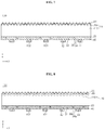
- FIG. 7 is a sectional view illustrating a solar cell in accordance with another embodiment of the present invention.
- FIG. 8 is a sectional view illustrating a solar cell in accordance with another embodiment of the present invention.
- FIG. 9 is a sectional view illustrating a solar cell in accordance with another embodiment of the present invention.
- FIG. 10 is a plan view of the solar cell illustrated in FIG. 9 ;
- FIG. 11 is a sectional view illustrating a solar cell in accordance with another embodiment of the present invention.
- FIG. 12 is a sectional view illustrating a solar cell in accordance with a further embodiment of the present invention.
- first and second and the like in the description, if any, are used for distinguishing between similar elements and not necessarily for describing a particular sequential or chronological order.
- FIG. 1 is a sectional view illustrating a solar cell in accordance with an embodiment of the present invention
- FIG. 2 is a partial rear plan view of the solar cell illustrated in FIG. 1 .
- the illustration of second electrode layers 422 and 442 of first and second electrodes 42 and 44 is omitted.
- the solar cell designated by reference numeral 100 , in accordance with the present embodiment includes a semiconductor substrate 10 , a first conductive area 32 disposed on one surface of the semiconductor substrate 10 , the first conductive area 32 being of a first conductive type, a second conductive area 34 of a second conductive type, which is the opposite of the first conductive type, and electrodes 42 and 44 including a first electrode 42 connected to the first conductive area 32 and a second electrode 44 connected to the second conductive area 34 .
- at least one of the first conductive area 32 and the second conductive area 34 is configured as a metal compound layer (e.g. a metal oxide layer).
- a tunneling layer 20 is formed over one surface of the semiconductor substrate 10 , and both the first conductive area 32 and the second conductive area 34 may be disposed over the tunneling layer 20 .
- the solar cell 100 may further include, for example, a front surface field forming layer 30 , a transparent conductive film 24 , and an anti-reflection film 26 . These components mentioned above will be described later in more detail.
- the semiconductor substrate 10 may include a base area 110 .
- the base area 110 may be formed of a crystalline semiconductor material including a first or second conductive dopant.
- the base area 110 may be formed of monocrystalline or polycrystalline semiconductors (e.g. monocrystalline or polycrystalline silicon) including a first or second conductive dopant.
- the base area 110 may be formed of monocrystalline semiconductors (e.g. a monocrystalline semiconductor wafer, and more specifically, a semiconductor silicon wafer), which includes an n-type or p-type dopant.
- monocrystalline semiconductors e.g. a monocrystalline semiconductor wafer, and more specifically, a semiconductor silicon wafer
- the first conductive area 32 having a p-type may be widely formed so as to form a junction (e.g. a pn junction), which produces carriers via photoelectric conversion, in conjunction with the base area 110 with the tunneling layer 20 interposed therebetween). In this way, an increased photoelectric conversion area may be accomplished.
- the first conductive area 32 which has a wide area, may effectively collect holes, which move relatively slowly, thereby contributing to further improvement in photoelectric conversion efficiency.
- the metal compound layer which constitutes the first or second conductive area 32 or 34 , may be easily formed because it is formed of an affordable material. The specific constituent materials of the first and second conductive areas 32 and 34 will be described later in detail. However, the embodiments of the present invention are not limited thereto, and the base area 110 may be of a p-type.
- the semiconductor substrate 10 may include only the base area 110 . That is, in a conventional solar cell, the semiconductor substrate 10 includes the base area 110 and a doping area that is of a different conductive type from the base area 110 , or includes the base area 110 and a doping area that is of the same conductive type as the base area 110 , but has a higher doping concentration than the base area 110 . On the other hand, in the present embodiment, the semiconductor substrate 10 includes only the base area 110 without a separate doping area.
- a dopant of the base area 110 may be an n-type or a p-type.
- the dopant may be selected from among group V elements such as, for example, phosphorous (P), arsenic (As), bismuth (Bi), and antimony (Sb).
- group V elements such as, for example, phosphorous (P), arsenic (As), bismuth (Bi), and antimony (Sb).
- the dopant of the base area 110 is of a p-type, the dopant may be selected from group III elements such as, for example, boron (B), aluminum (Al), gallium (Ga), and indium (In).
- the other surface (hereinafter referred to as a “front surface”) of the semiconductor substrate 10 may be subjected to texturing, and thus, may have protrusions having, for example, a pyramidal shape.
- the texturing structure formed on the semiconductor substrate 10 may have a given shape (for example, a pyramidal shape), which has an outer surface formed on a specific crystalline face of semiconductors.
- the back surface of the semiconductor substrate 10 may be formed into a relatively smooth flat surface having a lower surface roughness than the front surface via, for example, mirror surface grinding. This is because the properties of the solar cell 100 may considerably vary according to the properties of the back surface of the semiconductor substrate 10 when both the first and second conductive areas 32 and 34 are formed on the back surface of the semiconductor substrate 10 as in the present embodiment. Accordingly, no protrusion is formed, via texturing, on the back surface of the semiconductor substrate 10 so as to achieve improved passivation, which may consequently improve the properties of the solar cell 100 .
- the embodiments of the present invention are not limited thereto. In some cases, the back surface of the semiconductor substrate 10 may be provided with protrusions via texturing, and various other alterations are possible.
- the tunneling layer 20 may be formed over the back surface of the semiconductor substrate 10 .
- the tunneling layer 20 may be formed so as to come into contact with the back surface of the semiconductor substrate 10 , which may result in a simplified configuration and improved tunneling effects.
- the embodiments of the present invention are not limited thereto.
- the tunneling layer 20 serves as a barrier for electrons and holes, thereby preventing minority carriers from passing therethrough and allowing only majority carriers, which accumulate at a portion adjacent to the tunneling layer 20 and thus have a given amount of energy or more, to pass therethrough. At this time, the majority carriers, which have the given amount of energy or more, may easily pass through the tunneling layer 20 owing to tunneling effects.
- the tunneling layer 20 may serve as a diffusion barrier, which prevents the dopant of the conductive areas 32 and 34 from being diffused to the semiconductor substrate 10 .
- the tunneling layer 20 may comprise various materials to enable the tunneling of the majority carriers.
- the tunneling layer 20 may comprise oxides, nitrides, semiconductors, and conductive polymers.
- the tunneling layer 20 may comprise a silicon oxide, a silicon nitride, a silicon oxide nitride, intrinsic amorphous silicon, or intrinsic polycrystalline silicon.
- the tunneling layer 20 may be a silicon oxide layer comprising a silicon oxide. This is because the silicon oxide layer has excellent passivation and thus ensures easy tunneling of carriers.
- the silicon oxide layer may be formed via thermal oxidation or chemical oxidation.
- the tunneling layer 20 may be thinner than the anti-reflection film 26 and the first or second conductive area 32 or 34 .
- the thickness of the tunneling layer 20 may be 5 nm or less (more specifically, 2 nm or less, for example, within a range from 0.1 nm to 2 nm, more particularly, within a range from 0.1 nm to 1.5 nm).
- the thickness T of the tunneling layer 20 exceeds 5 nm, smooth tunneling does not occur, and consequently, the solar cell 100 cannot operate.
- the thickness of the tunneling layer 20 is below 0.1 nm, it may be difficult to form the tunneling layer 20 having the desired quality.
- the thickness of the tunneling layer 20 may be within a range from 0.5 nm to 2 nm, and more particularly, may be within a range from 0.5 nm to 1.5 nm.
- the embodiments of the present invention are not limited thereto, and the thickness of the tunneling layer 20 may have any of various values.
- the tunneling layer 20 may be formed throughout the back surface of the semiconductor substrate 10 . As such, the tunneling layer 20 may improve the passivation of the semiconductor substrate 10 and may be easily formed via a simplified process without patterning.
- the first and second conductive areas 32 and 34 which are located in the same plane, may be disposed over the tunneling layer 20 .
- the first and second conductive areas 32 and 34 may be formed so as to come into contact with the tunneling layer 20 , which may result in a simplified configuration and maximized tunneling effects.
- the embodiments of the present invention are not limited thereto.
- each of the first conductive area 32 and the second conductive area 34 may be a metal compound layer, which is formed of a metal compound.
- each of the first conductive area 32 and the second conductive area 34 may be a metal oxide layer comprising a metal oxide.
- the first conductive area 32 and the second conductive area 34 are configured as metal oxide layers as described above, easy manufacture, excellent chemical stability, and further improved passivation effects may be accomplished.
- the first conductive area 32 and the second conductive area 34 are formed of, for example, a sulfide, chemical stability may be low.
- the first conductive area 32 and the second conductive area 34 are formed of metal compounds, which are capable of selectively collecting electrons or holes in consideration of the energy band with relation to the semiconductor substrate 10 and the tunneling layer 20 . Accordingly, the first conductive area 32 and the second conductive area 34 do not include a semiconductor material that is included in the semiconductor substrate 10 , or a material that serves as an n-type or p-type dopant in the corresponding semiconductor material. This will be described below in more detail with reference to FIGS. 3 and 4 .
- FIG. 3 is a band diagram illustrating the semiconductor substrate 10 , the tunneling layer 20 , and the first conductive area 32 of the solar cell 100 in accordance with an embodiment of the present invention
- FIG. 4 is a band diagram illustrating the semiconductor substrate 10 , the tunneling layer 20 , and the second conductive area 34 of the solar cell 100 in accordance with an embodiment of the present invention.
- the semiconductor substrate 10 will be described below as being of an n-type by way of example.
- the semiconductor substrate 10 may be of an n-type, and the first conductive area 32 may be an emitter area, which selectively collects holes.
- the metal compound layer, which constitutes the first conductive area 32 capable of selectively collecting holes may have a lower Fermi level than the Fermi level of the semiconductor substrate 10 , and may have a greater work function than the work function of the semiconductor substrate 10 .
- the work function of the semiconductor substrate 10 may be approximately 3.7 eV
- the work function of the first conductive area 32 may be greater than 3.8 eV. More specifically, the work function of the first conductive area 32 may be 7 eV or less (for example, within a range from 3.8 eV to 7 eV).
- the first conductive area 32 When the work function of the first conductive area 32 exceeds 7 eV, the first conductive area 32 may have difficulty in selectively collecting holes. When the energy band gap is below 3.8 eV, the first conductive area 32 may have difficulty in selectively collecting only holes while excluding electrons.
- the semiconductor substrate 10 and the first conductive area 32 are aligned with and bonded to each other so that they have the same Fermi level value.
- holes present in the valence band of the semiconductor substrate 10 may easily move to the valence band of the first conductive area 32 by passing through the tunneling layer 20 .
- electrons in the semiconductor substrate 10 cannot pass through the tunneling layer 20 .
- the metal oxide layer which may be used as the first conductive area 32 described above, may be selected from among, for example, a molybdenum oxide layer formed of a molybdenum oxide, a tungsten oxide layer formed of a tungsten oxide (e.g. WO3), and a vanadium oxide layer formed of a vanadium oxide.
- a molybdenum oxide layer formed of a molybdenum oxide e.g. WO3
- tungsten oxide e.g. WO3
- vanadium oxide layer formed of a vanadium oxide e.g. WO3
- the first conductive area 32 may exhibit the excellent effect of selectively collecting holes.
- the semiconductor substrate 10 may be of an n-type, and the second conductive area 34 may be a field area (e.g. a back surface field area), which selectively collects electrons.
- the metal compound layer, which constitutes the second conductive area 34 capable of selectively collecting electrons may have a higher Fermi level than the Fermi level of the semiconductor substrate 10 and may have a smaller work function than the work function of the semiconductor substrate 10 .
- the work function of the semiconductor substrate 10 may be approximately 3.7 eV
- the work function of the second conductive area 34 may be within a range from 0.1 eV to 3.6 eV.
- the energy band gap between the conduction band of the second conductive area 34 and the conduction band of the semiconductor substrate 10 may be 1 eV or less (for example, within a range from 0.1 eV to 1 eV).
- the energy band gap described above exceeds 1 eV, the second conductive area 34 may have difficulty in selectively collecting electrons.
- the energy band gap described above is below 0.1 eV, the second conductive area 34 may have difficulty in selectively collecting only electrons while excluding holes because of the small energy band gap.
- the semiconductor substrate 10 and the second conductive area 34 are aligned with and bonded to each other so that they have the same Fermi level value.
- electrons present in the conduction band of the semiconductor substrate 10 may easily move to the conduction band of the second conductive area 34 by passing through the tunneling layer 20 .
- holes in the semiconductor substrate 10 cannot pass through the tunneling layer 20 .
- the metal oxide layer which may be used as the second conductive area 34 described above, may be selected from among, for example, a titanium oxide layer formed of a titanium oxide (e.g. TiO 2 ), and a zinc oxide layer formed of a zinc oxide (e.g. ZnO).
- a titanium oxide layer formed of a titanium oxide e.g. TiO 2
- a zinc oxide layer formed of a zinc oxide e.g. ZnO
- the second conductive area 34 may exhibit the excellent effect of selectively collecting electrons.
- the first conductive area 32 which selectively collects holes and transmits the holes to the first electrode 42 , serves as an emitter area.
- the second conductive area 34 which selectively collects electrons and transmits the electrons to the second electrode 44 , serves as a back surface field area.
- the thickness of each of the first conductive area 32 and the second conductive area 34 may be within a range from 1 nm to 100 nm.
- the first conductive area 32 and the second conductive area 34 may increase in resistance when the thickness thereof is increased because they are metal compound layers that include no dopant.
- the thickness of the first conductive area 32 or the second conductive area 34 may be set to 100 nm or less.
- the first or second conductive area 32 or 34 may not sufficiently show the role thereof.
- the embodiments of the present invention are not limited as to the thickness of the first and second conductive areas 32 and 34 .
- the first and second conductive areas 32 and 34 described above may be formed using various methods.
- the first and second conductive areas 32 and 34 may be formed using, for example, deposition or printing.
- the first conductive area 32 and the second conductive area 34 do not cause, for example, short circuits, even if they are located so that side surfaces thereof come into contact with each other, because the first and second conductive areas 32 and 34 include no dopant.
- a barrier area may be disposed over the tunneling layer 20 at a position between the first conductive area 32 and the second conductive area 34 so as to prevent the first conductive area 32 and the second conductive area 34 from coming into contact with each other.
- the barrier area may take the form of an empty space, or may have any of various configurations such as, for example, an intrinsic semiconductor layer or a configuration comprising a compound such as, for example, an oxide.
- the barrier area is illustrated in FIGS. 5 to 8 .
- first and second conductive areas 32 and 34 include no semiconductor material and no dopant applied to the semiconductor material as described above, recombination caused by such a dopant may be minimized.
- the first and second conductive areas 32 and 34 which are formed of metal compounds (e.g. metal oxides), serve as a passivation layer, resulting in improved passivation effects.
- various processes such as, for example, deposition of a semiconductor layer formed of a semiconductor material, doping, and activation thermal treatment may be omitted, and in particular, high-temperature processes may be omitted. In this way, the productivity of the solar cell 100 may be improved, and the semiconductor substrate 10 may maintain excellent properties.
- both the first and second conductive areas 32 and 34 are configured as the metal compound layers including no dopant.
- the embodiments of the present invention are not limited thereto, and only one of the first and second conductive areas 32 and 34 may be configured as a metal oxide layer including no dopant.
- Various other alterations are possible.
- the first conductive area 32 which collects different carriers (i.e. holes) from majority carriers of the base area 10 , may be wider than the second conductive area 34 , which collects the same carriers (i.e. electrons) as the majority carriers of the base area 110 .
- the first conductive area 32 which functions as an emitter area, may be sufficiently wide.
- the wide first conductive area 32 may effectively collect holes, which move relatively slowly.
- the electrodes 42 and 44 which are disposed on the back surface of the semiconductor substrate 10 , includes the first electrode 42 , which is electrically and physically connected to the first conductive area 32 , and the second electrode 44 , which is electrically and physically connected to the second conductive area 34 .
- the first electrode 42 may include a first electrode layer 421 and a second electrode layer 422 , which are stacked over the first conductive area 32 in sequence.
- the first electrode layer 421 may be relatively widely formed over (for example, in contact with) the first conductive area 32 .
- the first electrode layer 421 When the first electrode layer 421 is widely formed over the first conductive area 32 , carriers may easily reach the second electrode layer 422 by passing through the first electrode layer 421 , which may result in reduced resistance in the horizontal direction.
- the first conductive area 32 is configured as the metal compound layer, which is not doped and includes no dopant, may have high resistance, the first electrode layer 421 is provided in order to effectively reduce the resistance.
- the first electrode layer 421 may be formed of a material capable of transmitting light (i.e. a light-transmitting material). That is, the first electrode layer 421 may be formed of a transparent conductive material in order to enable the transmission of light and the easy movement of carriers. As such, the first electrode layer 421 does not prevent the transmission of light even if it is formed into a wide area over the first conductive area 32 .
- the first electrode layer 421 may comprise an indium tin oxide (ITO) or a carbon nano tube (CNT).
- ITO indium tin oxide
- CNT carbon nano tube
- the embodiments of the present invention are not limited thereto, and the first electrode layer 421 may comprise any of various other materials.
- the second electrode layer 422 may be formed over the first electrode layer 421 .
- the second electrode layer 422 may come into contact with the first electrode layer 421 , which may simplify the configuration of the first electrode 42 .
- the embodiments of the present invention are not limited thereto, and various alterations are possible such as, for example, an alteration in which a separate layer is present between the first electrode layer 421 and the second electrode layer 422 , are possible.
- the second electrode layer 422 disposed over the first electrode layer 421 , may be formed of a material having electrical conductivity superior to that of the first electrode layer 421 . As such, the efficiency by which the second electrode layer 422 collects carriers and a reduction in the resistance of the second electrode layer 422 may be further improved.
- the second electrode layer 422 may be formed of a metal, which is opaque or has lower transparency than the first electrode layer 421 and has electrical conductivity superior to that of the first electrode layer 421 .
- the second electrode layer 422 may have a given pattern so as to minimize shading loss.
- the second electrode layer 422 has a smaller area than the first electrode layer 421 . Thereby, light may be introduced into a portion at which the second electrode layer 422 is not formed.
- the plan shape of the second electrode layer 422 will be described later in more detail with reference to FIG. 2 .
- the first and second electrode layers 421 and 422 of the first electrode 42 may be formed using various methods.
- the first and second electrode layers 421 and 422 may be formed using, for example, deposition, sputtering, or printing.
- the second electrode 44 may include a first electrode layer 441 and a second electrode layer 442 , which are stacked over the second conductive area 34 in sequence.
- the role, material, and shape of the first and second electrode layers 441 and 442 of the second electrode 44 may be the same as the role, material, and shape of the first and second electrode layers 421 and 422 of the first electrode 42 except for the fact that the second electrode 44 is located over the second conductive area 34 , and therefore the description related to the first electrode 42 may be equally applied to the second electrode 44 .
- Insulation films which include, for example, a back surface passivation film, an anti-reflection film, and a reflection film, may be additionally formed over the first and second conductive areas 32 and 34 and/or the first electrode layers 421 and 441 on the back surface of the semiconductor substrate 10 .
- each of the first conductive area 32 and the second conductive area 34 are elongated to form stripes and are alternately arranged in the direction crossing the longitudinal direction thereof.
- a plurality of first conductive areas 32 which are spaced apart from one another, may be connected to one another at one edge
- a plurality of second conductive areas 34 which are spaced apart from one another, may be connected to one another at an opposite edge.
- the embodiments of the present invention are not limited thereto.
- the first conductive area 32 may be wider than the second conductive area 34 .
- the areas of the first conductive area 32 and the second conductive area 34 may be adjusted by providing the first and second conductive areas 32 and 34 with different widths. That is, the width W 1 of the first conductive area 32 may be greater than the width W 2 of the second conductive area 34 .
- the second electrode layer 422 of the first electrode 42 may take the form of stripes so as to correspond to the first conductive areas 32
- the second electrode layer 442 of the second electrode 44 may take the form of stripes so as to correspond to the second conductive areas 34 .
- the first electrode layer 421 of the first electrode 42 may be wider than the second electrode layer 422 and may take the form of stripes
- the first electrode layer 441 of the second electrode 44 may be wider than the second electrode layer 442 and may take the form of stripes.
- the striped portions of the first electrode 42 may be connected to one another at one edge
- the striped portions of the second electrode 44 may be connected to one another at an opposite edge.
- the embodiments of the present invention are not limited thereto.
- the front surface field forming layer 30 may be disposed over the front surface of the semiconductor substrate 10 .
- the front surface field forming layer 30 may be formed in contact with the front surface of the semiconductor substrate 10 so as to simplify the overall configuration and to maximize the formation effects of a field area.
- the embodiments of the present invention are not limited thereto.
- the front surface field forming layer 30 may be configured as a film having a fixed charge, or the metal compound layer, which is capable of selectively collecting electrons or holes as described above.
- the front surface field forming layer 30 may be an aluminum oxide layer comprising an aluminum oxide having a fixed charge.
- the front surface field forming layer 30 may be configured as a molybdenum oxide layer, a tungsten oxide layer, a vanadium oxide layer, a titanium oxide layer, or a zinc oxide layer, which may selectively collect electrons or holes.
- the front surface field forming layer 30 may be the combination of a plurality of layers described above.
- the front surface field forming layer 30 may be formed of the same layer as one of the metal compound layer, which constitutes the first or second conductive area 32 or 34 , which may simplify the manufacturing process.
- the front surface field forming layer 30 and the second conductive area 34 may be formed of a titanium oxide layer.
- the front surface field forming layer 30 described above may serve as a layer, which has a fixed charge and is not connected to the electrodes 42 and 44 , which are connected to an external circuit or another solar cell 100 , or may serve as a field area, which selectively collects electrons or holes so as to prevent the electrons and holes from being recombined with each other near the front surface of the semiconductor substrate 10 .
- the semiconductor substrate 10 includes only the base area 110 without a separate doping area, defects of the semiconductor substrate 10 may be minimized.
- the front surface field forming layer 30 may be formed of a compound (e.g. an oxide), thereby enabling the effective passivation of the front surface of the semiconductor substrate 10 .
- the thickness of the front surface field forming layer 30 may be equal to or less than the thickness of the first or second conductive area 32 or 34 . This is because the front surface field forming layer 30 does not serve to transfer carriers to the outside, and thus may have a relatively small thickness. In one example, the thickness of the front surface field forming layer 30 may be within a range from 1 nm to 10 nm. With this thickness, the front surface field forming layer 30 may exert sufficient effects thereof. However, the embodiments of the present invention are not limited as to the thickness of the front surface field forming layer 30 .
- the front surface of the semiconductor substrate 10 may be doped with a dopant, which is of the same conductive type as the base area 110 , at a high concentration, so as to form a doping area.
- the doping area may be used as a field area. The field area will be described below with relation to a front surface field forming layer (or field area) 30 a in the embodiment illustrated in FIG. 7 .
- the transparent conductive film 24 may be disposed over (for example, in contact with) the front surface of the semiconductor substrate 10 or the front surface field forming layer 30 .
- the transparent conductive film 24 is a floating electrode, which is not connected to an external circuit or another solar cell 100 .
- the floating electrode may prevent, for example, unnecessary ions from being collected on the surface of the semiconductor substrate 10 . In this way, it is possible to prevent degradation caused by, for example, ions (i.e. Potentially Induced Degradation (PID) in which the efficiency by which a solar cell module generates electricity is reduced in high-temperature and high-humidity environments).
- PID Potentially Induced Degradation
- the transparent conductive film 24 may comprise an indium tin oxide (ITO) or a carbon nano tube (CNT).
- ITO indium tin oxide
- CNT carbon nano tube
- the embodiments of the present invention are not limited thereto, and the transparent conductive film 24 may comprise any of various other materials.
- the transparent conductive film 24 may not be necessary, and may be not provided.
- the anti-reflection film 26 may be disposed over (for example, in contact with) the front surface of the semiconductor substrate 10 or the transparent conductive film 24 .
- the anti-reflection film 26 serves to reduce the reflectance of light introduced into the front surface of the semiconductor substrate 10 . As such, it is possible to increase the amount of light, which reaches the pn junction formed at the interface between the base area 110 and the first conductive area 32 . This may increase the short circuit current Isc of the solar cell 100 .
- the anti-reflection film 26 may be formed of various materials.
- the anti-reflection film 26 may be a single film or multiple films having the form of a combination of two or more films selected from among the group of a silicon nitride film, a silicon nitride film containing hydrogen, a silicon oxide film, a silicon oxide nitride film, an aluminum oxide film, a silicon carbide film, MgF 2 , ZnS, TiO 2 and CeO 2 films.
- the anti-reflection film 26 may be a single film formed of a silicon nitride, or may take the form of a stack in which a silicon nitride film and a silicon carbide film are stacked one above another.
- the front surface field forming layer 30 , the transparent conductive film 24 , and the anti-reflection film 26 may substantially be formed throughout the front surface of the semiconductor substrate 10 .
- the expression “formed throughout the front surface” includes the meaning of being physically completely formed over the entire front surface as well as the meaning of being formed so as to inevitably or unintentionally exclude a portion thereof. In this way, the manufacturing process may be simplified and each layer may sufficiently exert the role thereof.
- the solar cell 100 having a back surface electrode configuration in which the electrodes 42 and 44 are formed on the back surface of the semiconductor substrate 10 and no electrode is formed on the front surface of the semiconductor substrate 10 .
- shading loss may be minimized on the front surface of the semiconductor substrate 10 .
- the efficiency of the solar cell 100 may be improved.
- the embodiments of the present invention are not limited thereto.
- the second electrode layers 422 and 442 of the electrodes 42 and 44 may be widely formed in order to compensate for low resistance.
- the back surface electrode configuration may prevent problems attributable to shading loss.
- the first and second conductive areas 32 and 34 are formed over the semiconductor substrate 10 with the tunneling layer 20 interposed therebetween, the first and second conductive areas 32 and 34 are configured as layers separate from the semiconductor substrate 10 . Thereby, recombination loss may be minimized compared to the case where a doping area, which is formed by doping the semiconductor substrate 10 with a dopant, is used as a conductive area.
- the first and second conductive areas 32 and 34 include no semiconductor material and no dopant, problems caused by recombination may be minimized and passivation effects may be improved.
- the process of manufacturing the first and second conductive areas 32 and 34 may be simplified. In this way, the efficiency and productivity of the solar cell 100 may be improved.
- FIG. 5 is a sectional view illustrating a solar cell in accordance with another embodiment of the present invention
- FIG. 6 is a partial rear plan view of the solar cell illustrated in FIG. 5 .
- one of the first conductive area 32 and the second conductive area 34 , disposed over the tunneling layer 20 may include a metal compound layer, and the other one may be formed of a single semiconductor material.
- the front surface field forming layer 30 disposed over the front surface of the semiconductor substrate 10 , may include a metal compound layer.
- the first conductive area 32 may be formed of a single semiconductor material, and the second conductive area 34 may include a metal compound layer.
- the first conductive area 32 may comprise the same semiconductor material as the semiconductor substrate 10 (more specifically, a single semiconductor material, for example, silicon). As such, the first conductive area 32 may have properties similar to the semiconductor substrate 10 , and thus may minimize a difference in properties that may occur when the first conductive area 32 and the semiconductor substrate 10 comprise different semiconductor materials. In particular, because the first conductive area 32 is an emitter area that forms a pn junction, minimizing the difference in properties may improve the properties of the solar cell 100 .
- the first conductive area 32 may be formed over the semiconductor substrate 10 (more particularly, over the tunneling layer 20 ) separately from the semiconductor substrate 10 .
- the first conductive area 32 may have a different crystalline structure from the semiconductor substrate 10 , in order to be easily formed on the semiconductor substrate 10 .
- the first conductive area 32 may be configured as an amorphous, microcrystalline, or polycrystalline semiconductor layer (for example, an amorphous, microcrystalline, or polycrystalline silicon layer) doped with a first conductive dopant.
- the first conductive area 32 may be a polycrystalline semiconductor layer doped with a first conductive dopant.
- the first conductive area 32 is formed separately from the semiconductor substrate 10 , it is possible to prevent defects which may be caused when a doping area is formed in the semiconductor substrate 10 , or deterioration in open voltage. Thereby, the open voltage of the solar cell 100 may be increased.
- the embodiments of the present invention are not limited thereto. Accordingly, the first conductive area 32 may be configured as a doping area, which constitutes a portion of the semiconductor substrate 10 .
- the first conductive dopant may be of a p-type, and thus, the first conductive area 32 may be of a p-type.
- the first conductive dopant may be selected from among group III elements such as, for example, boron (B), aluminum (Al), gallium (Ga) and indium (In).
- the first conductive dopant may be added to a semiconductor layer, which constitutes the first conductive area 32 , in the process of forming the semiconductor layer.
- the semiconductor layer may be doped with the first conductive dopant using various doping methods such as, for example, thermal diffusion and ion implantation.
- the first conductive area 32 serves an emitter area, which produces carriers via photoelectric conversion by forming a pn junction (or a pn tunnel junction) in conjunction with the base area 110 with the tunneling layer 20 interposed therebetween.
- the semiconductor substrate 10 (more particularly, the base area 110 ) may be of a second conductive type (e.g. an n-type), and the first conductive area 32 may be of a conductive type, which is the opposite to the semiconductor substrate 10 (more particularly, the base area 110 ).
- the second conductive area 34 may comprise a different semiconductor material from the semiconductor substrate 10 (or the base area 110 ) and the first conductive area 32 .
- the semiconductor substrate 10 and the first conductive area 32 may comprise a single semiconductor material, whereas the second conductive area 34 may be formed of a semiconductor composite including two or more elements.
- the second conductive area 34 may be a metal compound layer (e.g. a metal oxide layer comprising a metal and oxygen, or oxide semiconductors), and thus may not comprise a semiconductor material (more specifically, a single semiconductor material such as, for example, silicon) included in the first conductive area 32 and the semiconductor substrate 10 .
- the second conductive area 34 does not include a semiconductor material included in the semiconductor substrate 10 , or an n-type or p-type dopant in the corresponding semiconductor material such as, for example, boron or phosphor.
- the second conductive area 34 may be a back surface field area, which forms a back surface field of the same conductive type as the semiconductor substrate 10 (more particularly, the base area 110 ) and has a higher doping concentration than the semiconductor substrate 10 .
- the second conductive area 34 may have a different crystalline structure from the semiconductor substrate 10 , in order to be easily formed over the semiconductor substrate 10 .
- the second conductive area 34 may be formed of oxide semiconductors, which are of a second conductive type, have an amorphous structure, and include a metal and oxygen, in the same manner as the front surface field forming layer 30 .
- the second conductive area 34 and the front surface field forming layer 30 are formed of oxide semiconductors as described above, the properties of the solar cell 100 may be improved owing to a difference in properties between the oxide semiconductors and the semiconductor material included in the first conductive area 32 .
- oxide semiconductors which form the front surface field forming layer 30 and the second conductive area 34 , will be described in detail.
- oxide semiconductors which form each of the front surface field forming layer 30 and the second conductive area 34 , may include only one group XII or group XIII metal, or may include a plurality of group XII or group XIII metals, along with oxygen.
- each of the front surface field forming layer 30 and the second conductive area 34 may be of an n-type due to, for example, electrons of oxygen, which remain rather than being coupled with the group XII or group XIII metal.
- the front surface field forming layer 30 and the second conductive area 34 which are formed of oxide semiconductors described above, may have, for example, a small light absorption coefficient, a wide energy band gap, and excellent mobility, which are suitable for the solar cell 100 .
- the oxide semiconductors which form each of the front surface field forming layer 30 and the second conductive area 32 , may be an oxide including indium, gallium and zinc (i.e. indium gallium zinc oxide (IGZO)).
- IGZO indium gallium zinc oxide
- indium may exist in an In 3+ ion state having an electron configuration of (1s) 2 (2s) 2 (2p) 6 (3s) 2 (3p) 6 (4s) 2 (3d) 10 (4p) 6 (4d) 10 (5s) 0 , thereby serving to form the movement path of electrons.
- the concentration of carriers is increased, resulting in increased conductivity.
- the concentration of carriers is reduced, resulting in reduced conductivity.
- Zinc may serve to stabilize an amorphous structure owing to tetrahedral coordination and to improve humidity resistance.
- Gallium has, for example, great oxygen affinity and coupling ability, and therefore may serve to prevent deterioration in electrical conductivity, which may be caused by oxygen.
- the amount of gallium is increased, the probability of coupling with oxygen may be increased and the concentration of carriers may be reduced, resulting in reduced conductivity.
- the concentration of carriers may be increased, resulting in increased conductivity. That is, gallium serves to adjust conductivity by adjusting the concentration of carriers.
- oxygen may provide excellent passivation properties. Passivation may be deteriorated when the amount of oxygen is reduced, and conductivity may be deteriorated when the amount of oxygen is increased.
- the amount of indium in each of the front surface field forming layer 30 and the second conductive area 34 , may be greater than each of the amount of gallium, the amount of zinc, and the amount of oxygen. This is because indium greatly contributes to improved conductivity.
- the amount of indium included in each of the front surface field forming layer 30 and the second conductive area 34 may be within a range from 50 at % to 90 at %. When the amount of indium is below 50 at %, the second conductive area 34 may have low conductivity, and thus may not function as desired. When the amount of indium exceeds 90 at %, the amount of gallium or zinc is reduced, which makes it difficult to achieve desired properties.
- the amount of zinc may be equal to or greater than the amount of gallium, and may be equal to or greater than the amount of oxygen.
- the amount of zinc may be greater than the amount of gallium and may be greater than the amount of oxygen. This is because zinc may improve structural stability.
- the amount of zinc included in each of the front surface field forming layer 30 and the second conductive area 34 may be within a range from 10 at % to 40 at %. When the amount of zinc is below 10 at %, the effects caused by zinc may not be sufficient. When the amount of zinc exceeds 40 at %, the non-uniformity of mobility and conductivity may be increased.
- gallium may be included in order to adjust the concentration of carriers and electrical conductivity. In addition, gallium may improve the passivation properties of the second conductive area 34 . In one example, the amount of gallium may be within a range from 1 at % to 10 at %. When the amount of gallium is within a range from 1 at % to 10 at %, each of the front surface field forming layer 30 and the second conductive area 34 may have desired conductivity.
- the remainder excluding indium, zinc and gallium, may be oxygen.
- the amount of oxygen included in each of the front surface field forming layer 30 and the second conductive area 34 may be within a range from 1 at % to 10 at %. Passivation may be deteriorated when the amount of oxygen is below 1 at %, and conductivity may be reduced when the amount of oxygen exceeds 10 at %.
- the embodiments of the present invention are not limited thereto, and the quantities of indium, zinc, gallium and oxygen may have various values.
- the front surface field forming layer 30 or the second conductive area 34 comprises a transition metal such as, for example, nickel (Ni) or copper (Cu), an alkali metal, and an alkali earth metal, excluding, for example, zinc
- the front surface field forming layer 30 or the second conductive area 34 may have difficulty in exhibiting semiconductor properties, or may not be suitable for the formation of an electric field.
- the front surface field forming layer 30 or the second conductive area 34 is formed only of a gallium oxide without comprising zinc and indium
- the front surface field forming layer 30 or the second conductive area 34 may be vulnerable to acids and alkalis, which are used in chemical processes (e.g. a washing process and a patterning process) included in the manufacture of the solar cell 100 , and thus may have low chemical resistance.
- the gallium oxide may have insufficient conductivity or may have difficulty in forming a strong electric field, and thus may not be suitable for use in the front surface field forming layer 30 or the second conductive area 34 .
- the proportion of oxygen is increased compared to IGZO because zinc, which may improve structural stability and humidity resistance, is not included.
- the indium oxide may have relatively low conductivity. Accordingly, the indium oxide may not be suitable for use in the front surface field forming layer 30 or the second conductive area 34 .
- the indium oxide may suffer from increased non-uniformity of mobility and conductivity because it comprises no zinc.
- the second conductive area 34 may be vulnerable to heat, and thus may have low temperature stability. Thereby, when the second conductive area 34 is applied to the solar cell 100 , for example, hot spots or heat damping may occur, or properties of the second conductive area 34 may deteriorate over time, which may deteriorate the reliability and efficiency of the solar cell 100 .
- the electric field of conductivity of the zinc oxide may not be good enough to be used in the front surface field forming layer 30 or the second conductive area 34 .
- the front surface field forming layer 30 or the second conductive area 34 may be vulnerable to acids and alkalis, which are used in chemical processes (e.g. a washing process and a patterning process) included in the manufacture of the solar cell 100 , and thus may have low chemical resistance.
- the front surface field forming layer 30 and the second conductive area 34 comprise indium, zinc, and gallium, along with oxygen, which may improve various properties suitable for the front surface field forming layer 30 and the second conductive area 34 .
- the embodiments of the present invention are not limited thereto, and an embodiment in which the front surface field forming layer 30 or the second conductive area 34 comprises at least one of indium, zinc, and gallium may be included in the present invention.
- oxide semiconductors which form the front surface field forming layer 30 and the second conductive area 34 , comprise a different material from a semiconductor material (more specifically, a single semiconductor material, for example, group IV elements) of the first conductive area 32 , and thus may have properties different from those of the first conductive area 32 .
- the front surface field forming layer 30 or the second conductive area 34 may have a greater energy band gap than the first conductive area 32 .
- the energy band gap of the front surface field forming layer 30 or the second conductive area 34 may be within a range from 3.0 eV to 3.5 eV
- the energy band gap of the first conductive area 32 may be within a range from 1.1 eV to 1.2 eV.
- the open voltage may further be increased.
- the front surface field forming layer 30 or the second conductive area 34 may have a smaller light absorption coefficient than the first conductive area 32 .
- the light absorption coefficient of each of the front surface field forming layer 30 and the second conductive area 34 may be within a range from 0.1 ⁇ 10 3 /cm 3 to 5 ⁇ 10 3 /cm 3
- the light absorption coefficient of the first conductive area 32 may be within a range from 4 ⁇ 10 5 /cm 3 to 6 ⁇ 10 5 /cm 3 .
- the light absorption coefficient of the front surface field forming layer 30 and the second conductive area 34 has a small value, light introduced into the solar cell 100 may be absorbed by the front surface field forming layer 30 and the second conductive area 34 , which may reduce light loss.
- the front surface field forming layer 30 which has a small light absorption coefficient, is disposed on the front surface into which a relatively great amount of light is introduced, which may minimize the loss of light due to absorption.
- the mobility of electrons in the oxide semiconductors, which form each of the front surface field forming layer 30 and the second conductive area 34 may be within a range from 5 cm 2 /Vsec to 100 cm 2 /Vsec. Thereby, electrons may smoothly move from the second conductive area 34 and be collected by the second electrode 44 .
- the second conductive area 34 and the second electrode 44 may maintain ohmic contact.
- the work function of the second conductive area 34 may be greater than the work function of the second electrode 44 .
- the work function of the second conductive area 34 may be within a range from 4.60 Ev to 4.85 Ev. Thereby, electrons in the second conductive area 34 may smoothly move to the second electrode 44 .
- the concentration of carriers in the front surface field forming layer 30 or the second conductive area 34 may be within a range from 5 ⁇ 10 18 /cm 3 to 1 ⁇ 10 20 /cm 3 . Within this range, the second conductive area 34 may have low resistance and the front surface field forming layer 30 may form a strong electric field.
- the sheet resistance of the second conductive area 34 may have a value of 400 ohm/sq or less. When the sheet resistance of the second conductive area 34 is below 400 ohm/sq, the second conductive area 34 may have difficulty in satisfactorily performing the role thereof. In one example, the sheet resistance of the second conductive area 34 may be within a range from 150 ohm/sq to 350 ohm/sq.
- the properties of the second conductive area 34 may be improved even if the thickness of the second conductive area 34 is not greatly increased.
- the sheet resistance of the second conductive area 34 may be varied by adjusting the composition as described above.
- the resistance of the second conductive area 34 may be reduced as the amount of indium is increased and the amount of gallium is reduced in the second conductive area 34 .
- the concentration of carriers and the sheet resistance of the second conductive area 34 may be varied owing to the conditions of a heat treatment process, which is performed after the front surface field forming layer 30 and the second conductive area 34 are formed.
- the front surface field forming layer 30 and the second conductive area 34 may have, for example, the concentration of carriers and the resistance described above when the pressure of oxygen is maintained at 5 Pa or less.
- the heat treatment temperature is approximately within a range from 250 ⁇ to 450 ⁇ (for example, a range from 300 ⁇ to 350 ⁇ )
- the second conductive area 34 may have, for example, the concentration of carriers and the resistance described above.
- the thickness of the front surface field forming layer 30 or the second conductive area 34 may be within a range from 100 nm to 400 nm. At this thickness, the front surface field forming layer 30 or the second conductive area 34 may have low resistance and sufficient conductivity. In one example, the thickness of the front surface field forming layer 30 may be smaller than the thickness of the second conductive area 34 . Because the second conductive area 34 must have low resistance in order to improve connection with the second electrode 44 , the second conductive area 34 may have a sufficient thickness. On the other hand, the front surface field forming layer 30 must have a small thickness, which is enough to form an electric field, in order to minimize light absorption. However, the embodiments of the present invention are not limited thereto.
- the mobility of electrons, the work function, the concentration of carriers, the sheet resistance, and the thickness of the front surface field forming layer 30 or the second conductive area 34 described above are proposed by way of example. Accordingly, the embodiments of the present invention are not limited to the values described above, and may have various other values.
- the front surface field forming layer 30 and the second conductive area 34 may be formed via a simplified process at a relatively low temperature. More specifically, the front surface field forming layer 30 and the second conductive area 34 may be formed by performing sputtering using a target, which comprises indium, gallium, zinc and oxygen, and then performing heat treatment at a temperature within a range from 250° C. to 450° C. (for example, a range from 300° C. to 350° C.).
- IGZO IGZO powder
- MOCVD organic metal chemical vapor deposition
- a separator area 36 which takes the form of, for example, an empty space or a trench, is located between the first conductive area 32 and the second conductive area 34 , which are formed of different materials as described above. As such, the first conductive area 32 and the second conductive area 34 may be spaced apart from each other with the separator area 36 interposed therebetween. The separator area 36 physically separates the first conductive area 32 and the second conductive area 34 from each other, thereby preventing problems such as, for example, shunt, which may occur between the first conductive area 32 and the second conductive area 34 . In this way, the charge density of the solar cell 100 may be increased. In one example, the solar cell 100 may have the charge density of 82% or more.
- the separator area 36 may be formed in the entire gap between the first conductive area 32 and the second conductive area 34 so as to completely separate the first and second conductive areas 32 and 34 from each other as illustrated in FIG. 6 , or may be formed in a part of the gap between the first conductive area 32 and the second conductive area 34 . As such, the first conductive area 32 and the second conductive area 34 may come into contact with each other at the remaining part of the boundary therebetween. In addition, the separator area 36 may not be necessary, and the first conductive area 32 and the second conductive area 34 may wholly come into contact with each other. Various other alterations are possible.
- the present embodiment illustrates that the separator area 36 , which takes the form of an empty space or a trench, is located between the first conductive area 32 and the second conductive area 34 .
- the embodiments of the present invention are not limited thereto. Accordingly, another part, rather than the separator area 36 , may be located between the first conductive area 32 and the second conductive area 34 . This will be described later in detail with reference to FIG. 8 .
- An insulation layer 40 may be formed over the first and second conductive areas 32 and 34 .
- the insulation layer 40 may be formed so as to cover the upper surface (the lower surface of the semiconductor substrate 10 in FIG. 5 ) and the side surface of the first and second conductive areas 32 and 34 and may also be formed inside the separator area 36 .
- the insulation layer 40 may be formed over (for example, in contact with) the tunneling layer 20 at portions corresponding to the upper surface and the side surface of the first and second conductive areas 32 and 34 , and the separator area 36 , which is located between the first and second conductive areas 32 and 34 .
- the passivation properties of the first and second conductive areas 32 and 34 may be improved, and shunt between the first and second conductive areas 32 and 34 may be more effectively prevented.
- the insulation layer 40 includes a first opening 402 for connection between the first conductive area 32 and the first electrode 42 , and a second opening 404 for connection between the second conductive area 34 and the second electrode 44 .
- the insulation layer 40 serves to prevent the first conductive area 32 and the second conductive area 34 from being connected to incorrect electrodes (i.e. the second electrode 44 in the case of the first conductive area 32 and the first electrode 42 in the case of the second conductive area 34 ).
- the insulation layer 40 may have the passivation effects of the first and second conductive areas 32 and 34 and/or the tunneling layer 20 .
- the insulation layer 40 may be thicker than the tunneling layer 20 . Thereby, the insulation and passivation properties of the insulation layer 40 may be improved.
- the embodiments of the present invention are not limited thereto.
- the insulation layer 40 may be formed of various insulation materials (e.g. an oxide and a nitride).
- the insulation layer 40 may have a single film structure of any one selected from the group consisting of a silicon nitride film, a silicon nitride film containing hydrogen, a silicon oxide film, a silicon oxide nitride film, Al 2 O 3 , MgF 2 , ZnS, TiO 2 , and CeO 2 , or a multi-layer film structure in the form of a combination of two or more films.
- the embodiments of the present invention are not limited thereto and the insulation layer 40 may of course be formed of various other materials.
- the anti-reflection film 26 and the insulation layer 40 may not include a dopant in order to achieve excellent insulation and passivation properties.
- the electrodes 42 and 44 disposed on the back surface of the semiconductor substrate 10 , include the first electrode 42 , which is electrically and physically connected to the first conductive area 32 , and the second electrode 44 , which is electrically and physically connected to the second conductive area 34 .
- the first electrode 42 passes through the first opening 402 of the insulation layer 40 and is connected to (for example, in contact with) the first conductive area 32 , and includes the second electrode layer 422 formed of a metal material
- the second electrode 44 passes through the second opening 404 of the insulation layer 40 and is connected to (for example, in contact with) the second conductive area 34 , and includes the second electrode layer 442 formed of a metal material.
- the first and second electrodes 42 and 44 may be formed of various conductive materials (e.g., metal materials).
- FIG. 6 illustrates that the separator area 36 takes the form of stripes, which extend in a given direction by a long length between the first conductive area 32 and the second conductive area 34 so as to cause the first and second conductive areas 32 and 34 to be wholly spaced apart from each other.
- the embodiments of the present invention are not limited thereto, and the shape of the separator area 36 may be altered in various ways.
- the base area 110 of the semiconductor substrate 10 may have a lower doping concentration, higher resistance, or lower concentration of carriers than one of the first and second conductive areas 32 and 34 , which is of the same conductive type as the base area 110 .
- the second conductive area 34 is formed of oxide semiconductors comprising oxygen and a metal, the base area 110 may have a higher resistance and lower concentration of carriers than the second conductive area 34 when the base area 110 is of a second conductive type.
- the concentration of carriers of the base area 110 may be within a range from 0.1 ⁇ 10 15 /cm 3 to 7 ⁇ 10 15 /cm 3
- the concentration of carriers of the second conductive area 34 may be within a range from 5 ⁇ 10 18 /cm 3 to 1 ⁇ 10 20 /cm 3 . This will be described later in more detail.
- the base area 110 is of a first conductive type
- the base area 110 may have a lower doping concentration, higher resistance, or lower concentration of carriers than the first conductive area 32 .
- each of the front surface field forming layer 30 and the second conductive area 34 comprises oxide semiconductors.
- the embodiments of the present invention are not limited thereto. Accordingly, only one of the front surface field forming layer 30 and the second conductive area 34 may comprise oxide semiconductors.
- the front surface field forming layer 30 may be formed by doping a semiconductor layer (e.g. an amorphous semiconductor layer, a microcrystalline semiconductor layer, or a polycrystalline semiconductor layer), which is separate from the semiconductor substrate 10 , with a second conductive dopant.
- the front surface field forming layer 30 may be configured as a field area, which functions similar to a layer (e.g. a passivation film and/or the anti-reflection film 26 ), which is formed close to the semiconductor substrate 10 and is doped with a fixed charge.
- the passivation film or the anti-reflection film 26 may be formed of an oxide (e.g.
- the semiconductor substrate 10 may include only the base area 110 without a separate doping area, which may minimize defects of the semiconductor substrate 10 .
- the front surface field forming layer 30 having various configurations may be formed using various other methods. Other examples will be described below in detail with reference to FIGS. 7 and 8 .
- the second conductive area 34 comprises oxide semiconductors when the semiconductor substrate 10 is of an n-type and the second conductive area 34 is of the same n-type, and thus forms a back surface field area.
- the embodiments of the present invention are not limited thereto. Accordingly, when the semiconductor substrate 10 is of a p-type and the first conductive area 32 is of an n-type to thereby form an emitter area, the first conductive area 32 may comprise oxide semiconductors.
- the first conductive area 32 may comprise oxide semiconductors.
- Various other alterations are possible.
- FIG. 7 is a sectional view illustrating a solar cell in accordance with another embodiment of the present invention.
- a front surface field forming layer (or a field area) 30 a may be configured as a doping area, which is formed by doping the semiconductor substrate 10 with a second conductive dopant at a relatively high doping concentration. That is, the front surface field forming layer 30 a comprises crystalline (monocrystalline or polycrystalline) semiconductors of a second conductive type, and constitutes a portion of the semiconductor substrate 10 . In one example, the front surface field forming layer 30 a may constitute a portion of a monocrystalline semiconductor substrate (e.g. a monocrystalline silicon wafer substrate) of a second conductive type. In addition, the doping concentration of the front surface field forming layer 30 a may be greater than the doping concentration of the base area 110 .
- the front surface field forming layer 30 a is formed via a doping process, a process of forming a separate layer in order to form the front surface field forming layer 30 may be omitted, which may reduce the burden on the manufacturing process.
- only the second conductive area 34 comprises oxide semiconductors.
- FIG. 8 is a sectional view illustrating a solar cell in accordance with another embodiment of the present invention.
- a second conductive area 34 a may comprise a single semiconductor material of a second conductive type, and only the front surface field forming layer 30 may comprise oxide semiconductors.
- the second conductive area 34 a has properties that are the same or similar to those of the first conductive area 32 except that it is of the second conductive type, and thus a description thereof will be omitted below.
- a barrier area 36 a may be located between the first conductive area 32 and the second conductive area 34 a .
- the insulation layer 40 may be formed so as to come into contact with the first and second conductive areas 32 and 34 a and the barrier area 36 a.
- first conductive area 32 and the second conductive area 34 a are spaced apart from each other by the barrier area 36 a located therebetween.
- shunt may occur, thus causing deterioration in the performance of the solar cell 100 . Accordingly, in the present embodiment, unnecessary shunt may be prevented owing to the barrier area 36 a located between the first conductive area 32 and the second conductive area 34 a.
- the barrier area 36 a may comprise any of various materials, which may substantially insulate the first conductive area 32 and the second conductive area 34 a from each other. That is, an undoped insulation material (e.g. an oxide or a nitride) may be used to form the barrier area 36 a . Alternatively, the barrier area 36 a may comprise intrinsic semiconductors. At this time, the first conductive area 32 , the second conductive area 34 a , and the barrier area 36 a may be successively formed so as to come into contact with one another at the side surfaces thereof using the same semiconductor material (e.g. amorphous silicon, microcrystalline silicon, or polycrystalline silicon), and the barrier area 36 a may substantially include no dopant.
- an undoped insulation material e.g. an oxide or a nitride
- the barrier area 36 a may comprise intrinsic semiconductors.
- the first conductive area 32 , the second conductive area 34 a , and the barrier area 36 a may be successively formed so as to come into contact
- a portion of the semiconductor layer is doped with a first conductive type dopant so as to form the first conductive area 32 and a portion of the remaining semiconductor layer is doped with a second conductive type dopant so as to form the second conductive area 34 a .
- a portion at which the first conductive area 32 and the second conductive area 34 a are not formed may configure the barrier area 36 a . In this way, the manufacture of the first conductive area 32 , the second conductive area 34 a and the barrier area 36 a may be simplified.
- the embodiments of the present invention are not limited thereto.
- the thickness of the barrier area 36 a may be different from those of the first conductive area 32 and the second conductive area 34 a .
- the barrier area 36 a may be thicker than the first conductive area 32 and the second conductive area 34 a .
- the barrier area 36 a may be thinner than the first conductive area 32 and the second conductive area 34 a .
- the basic constituent material of the barrier area 36 a may be different from those of the first conductive area 32 and the second conductive area 34 a.
- the present embodiment illustrates that the first conductive area 32 and the second conductive area 34 a are wholly spaced apart from each other by the barrier area 36 a .
- the embodiments of the present invention are not limited thereto.
- the barrier area 36 a may be formed so as to cause the first conductive area 32 and the second conductive area 34 a to be spaced apart from each other only at a portion of the boundary therebetween. Thereby, the first conductive area 32 and the second conductive area 34 a may come into contact with each other at the remaining boundary therebetween.
- the barrier area 36 a may not be necessary, and the first conductive area 32 and the second conductive area 34 a may wholly come into contact with each other.
- Various other alterations are possible.
- the present embodiment illustrates that the second conductive area 34 a comprises a single semiconductor material (e.g. silicon), rather than comprising oxide semiconductors, in the same manner as the first conductive area 32 , and the barrier area 36 a is formed.
- the first conductive area 32 or the second conductive area 34 a may comprise oxide semiconductors and the barrier area 36 a may be provided.
- the second conductive area 34 a may comprise a single semiconductor material (e.g. silicon), rather than comprising oxide semiconductors, in the same manner as the first conductive area 32 , and the separator area 36 may be formed.
- Various other alterations are possible.
- FIG. 9 is a sectional view illustrating a solar cell in accordance with another embodiment of the present invention
- FIG. 10 is a plan view of the solar cell illustrated in FIG. 9 .
- the illustration of FIG. 10 is focused on the semiconductor substrate and the electrodes.
- FIGS. 9 and 10 a detailed description related to parts that are the same or similar to those of the embodiments with reference to FIGS. 5 to 8 will be omitted below and the following description will be focused on different parts.
- the first conductive area 32 is disposed on one surface of the semiconductor substrate 10 and the second conductive area 34 is disposed on the other surface of the semiconductor substrate 10 .
- the first conductive area 32 may be formed throughout one surface of the semiconductor substrate 10
- the second conductive area 34 may be formed throughout the other surface of the semiconductor substrate 10 .
- the present embodiment may not include the front surface field forming layer 30 or the front surface field area 30 a , unlike the embodiments with reference to FIGS. 1 to 8 .
- the first conductive area 32 may be disposed over the tunneling layer 20 , which is formed over one surface (e.g. the back surface) of the semiconductor substrate 10 .
- the first conductive area 32 may be disposed in contact with the tunneling layer 20 .
- the first conductive area 32 may be of a first conductive type, i.e. a p-type.
- the semiconductor substrate 10 or the base area 110 may be of a second conductive type, i.e. an n-type.
- the first conductive area 32 may form a pn junction (or a pn tunnel junction) in conjunction with the base area 110 with the tunneling layer 20 interposed therebetween and may configure an emitter area, which produces carriers via photoelectric conversion.
- the second conductive area 34 may be of a second conductive type, i.e. an n-type and may configure a front surface field area, which forms a front surface field having the same conductive type as the semiconductor substrate 10 .
- the second conductive area 34 may be separately formed over the semiconductor substrate 10 , and may have a different crystalline structure from the semiconductor substrate 10 in order to be easily formed on the semiconductor substrate 10 .
- the first conductive area 32 may be configured as a single semiconductor (e.g. silicon) layer
- the second conductive area 34 may be configured as an oxide semiconductor layer.
- a detailed description related to the single semiconductor layer, which forms the first conductive area 32 , and the oxide semiconductor layer, which forms the second conductive area 34 is the same as or similar to the above description of the embodiments with reference to FIGS. 5 to 8 , and thus will be omitted below.
- the anti-reflection film 26 may substantially be formed throughout the front surface of the semiconductor substrate 10 over the second conductive area 34 excluding the opening 404 , which corresponds to the second electrode 44 . In one example, the anti-reflection film 26 may be formed so as to be come into contact with the second conductive area 34 .
- An anti-reflection film 40 a may substantially be formed throughout the back surface of the semiconductor substrate 10 over the first conductive area 32 excluding the opening 402 , which corresponds to the first electrode 42 .
- the anti-reflection film 40 a may be formed so as to come into close contact with the first conductive area 32 .
- the anti-reflection film 40 a may be formed of various materials.
- the anti-reflection film 40 a may be a single film or multiple films having the form of a combination of two or more films selected from among the group of a silicon nitride film, a silicon nitride film containing hydrogen, a silicon oxide film, a silicon oxide nitride film, an aluminum oxide film, a silicon carbide film, an aluminum oxide film, MgF 2 , ZnS, TiO 2 and CeO 2 films.
- the anti-reflection film 40 a may be a single silicon nitride film, or may take the form of a stack in which a silicon nitride film and a silicon carbide film are stacked one above another.
- the embodiments of the present invention are not limited thereto and the anti-reflection film 40 a may of course be formed of any of various materials.
- the anti-reflection film 40 a may be replaced with a passivation film, or another film such as, for example, the insulation layer 40 or the reflection film of the embodiment with reference to FIG. 5 may be formed on the first conductive area 32 or the back surface of the semiconductor substrate 10 .
- Various other alterations are possible.
- the first electrode 42 may be disposed on (for example, in contact with) the first conductive area 32 so as to be electrically connected to the first conductive area 32 , and may include the second electrode layer 422 formed of a metal material.
- the second electrode 44 may be disposed on (for example, in contact with) the second conductive area 34 so as to be electrically connected to the second conductive area 34 , and may include the second electrode layer 442 formed of a metal material.
- the first and second electrodes 42 and 44 may be electrically connected to the first and second conductive areas 32 and 34 through the openings 402 and 404 formed in the anti-reflection films 40 a and 26 (i.e. by penetrating the anti-reflection films 40 a and 26 ).
- the shape of the first and second electrodes 42 and 44 will again be described below with reference to FIG. 10 .
- first and second electrodes 42 and 44 (more accurately, the second electrode layers 422 and 442 ) will be described in detail with reference to FIG. 10 .
- the first and second electrodes 42 and 44 may include a plurality of finger electrodes 42 a and 44 a , which are spaced apart from one another at a constant pitch.
- FIG. 10 illustrates that the finger electrodes 42 a and 44 a are parallel to one another and are also parallel to the edge of the semiconductor substrate 10 , the embodiments of the present invention are not limited thereto.
- the first and second electrodes 42 and 44 may include bus bar electrodes 42 b and 44 b , which are formed in the direction crossing the finger electrodes 42 a and 44 a so as to connect the finger electrodes 42 a and 44 a to one another.
- bus bar electrode 42 b or 44 b Only one bus bar electrode 42 b or 44 b may be provided, or a plurality of bus bar electrodes 42 b or 44 b may be arranged at a larger pitch than the pitch of the finger electrodes 42 a and 44 a as exemplarily illustrated in FIG. 10 .
- the width of the bus bar electrodes 42 b and 44 b may be larger than the width of the finger electrodes 42 a and 44 a
- the embodiments of the present invention are not limited thereto. Accordingly, the width of the bus bar electrodes 42 b and 44 b may be equal to or less than the width of the finger electrodes 42 a and 44 a.
- both the finger electrode 42 a and the bus bar electrode 42 b of the first electrode 42 may be formed so as to penetrate the anti-reflection film 40 a . That is, the opening 402 may be formed so as to correspond to both the finger electrode 42 a and the bus bar electrode 42 b of the first electrode 42 . In addition, both the finger electrode 44 a and the bus bar electrode 44 b of the second electrode 44 may be formed so as to penetrate the anti-reflection film 26 . That is, the opening 404 may be formed so as to correspond to both the finger electrode 44 a and the bus bar electrode 44 b of the second electrode 44 .
- the embodiments of the present invention are not limited thereto.
- the finger electrode 42 a of the first electrode 42 may be formed so as to penetrate the anti-reflection film 40 a and the bus bar electrode 42 b may be formed over the anti-reflection film 40 a .
- the opening 402 may have a shape corresponding to the shape of the finger electrode 42 a , and may not be formed in a portion at which only the bus bar electrode 42 b is located.
- the finger electrode 44 a of the second electrode 44 may be formed so as to penetrate the anti-reflection film 26 and the bus bar electrode 44 b may be formed over the anti-reflection film 26 .
- the opening 404 may have a shape corresponding to the shape of the finger electrode 44 a , and may not be formed in a portion at which only the bus bar electrode 44 b is located.
- FIG. 10 illustrates that the first electrode 42 and the second electrode 44 have the same plan shape.
- the embodiments of the present invention are not limited thereto, and, for example, the width and pitch of the finger electrode 42 a and the bus bar electrode 42 b of the first electrode 42 may be different from the width and pitch of the finger electrode 44 a and the bus bar electrode 44 b of the second electrode 44 .
- the first electrode 42 and the second electrode 44 may have different plan shapes, and various other alterations are possible.
- protrusions are formed on the front surface and the back surface of the semiconductor substrate 10
- the embodiments of the present invention are not limited thereto.
- protrusions may be formed on only one of the front surface and the back surface of the semiconductor substrate 10 .
- protrusions may be formed on the front surface of the semiconductor substrate 10 , and the back surface of the semiconductor substrate 10 may be subjected to mirror surface grinding, which may minimize the reflection of light from the front surface, into which a relatively great amount of light is introduced, and may enable the reuse of light in the back surface via reflection.
- no protrusion may be formed on the front surface and the back surface of the semiconductor substrate 10 .
- the solar cell 100 has a bi-facial structure to allow light to be introduced into the front surface and the back surface of the semiconductor substrate 10 .
- the amount of light for use in the solar cell 100 may be increased, which may contribute to improvement in the efficiency of the solar cell 100 .
- the embodiments of the present invention are not limited thereto, and the second electrode 44 may be formed throughout the back surface of the semiconductor substrate 10 .
- Various other alterations are possible.
- the first conductive area 32 is formed of oxide semiconductors different from a semiconductor material of the second conductive area 34 and the semiconductor substrate 10 .
- the first conductive area 32 may have different properties from the second conductive area 34 , which may minimize surface recombination and light loss and may achieve high energy band gap. In this way, the open voltage (open circuit voltage or opening voltage) and current density of the solar cell 100 may be increased, resulting in improved efficiency of the solar cell 100 .
- the semiconductor substrate 10 is of a second conductive type so that the first conductive area 32 disposed on the back surface thereof forms an emitter area and the second conductive area 34 disposed on the front surface thereof forms a front surface field area.
- the embodiments of the present invention are not limited thereto, and the semiconductor substrate 10 may be of a first conductive type so that the first conductive area 32 disposed on the back surface thereof forms a back surface field area and the second conductive area 34 disposed on the front surface thereof forms an emitter area.
- the semiconductor substrate 10 may be of a first conductive type so that the first conductive area 32 disposed on the back surface thereof forms a back surface field area and the second conductive area 34 disposed on the front surface thereof forms an emitter area.
- Various other alterations are possible.
- FIG. 11 is a sectional view illustrating a solar cell in accordance with another embodiment of the present invention.
- a detailed description related to parts that are the same or similar to those of the embodiment with reference to FIGS. 9 and 10 will be omitted below and the following description is focused on different parts.
- another tunneling layer 22 is located between the semiconductor substrate 10 and the second conductive area 34 .
- the description related to the tunneling layer 20 with reference to FIG. 9 may be directly applied to the tunneling layer 22 located between the semiconductor substrate 10 and the second conductive area 34 , and thus a description thereof will be omitted below.
- the tunneling layer 22 which is additionally located between the semiconductor substrate 10 and the second conductive area 34 , may maximize passivation effects and may ensure smooth movement of carries.
- FIG. 12 is a sectional view illustrating a solar cell in accordance with a further embodiment of the present invention.
- a detailed description related to parts that are the same or similar to those of the embodiment with reference to FIGS. 9 and 10 will be omitted below and the following description is focused on different parts.
- the first conductive area 32 which comprises the same semiconductor material as the semiconductor substrate 10
- the first electrode 42 which is connected to the first conductive area 32
- the second conductive area 34 which comprises a semiconductor material (e.g. composite semiconductors or oxide semiconductors) different from a semiconductor material of the semiconductor substrate 10
- the second electrode 44 which is connected to the second conductive area 34
- the semiconductor substrate 10 may be of a second conductive type, i.e. an n-type.
- the first conductive area 32 which is of a p-type and forms an emitter area, may be disposed on the front surface of the semiconductor substrate 10 , so as to minimize the path of light that reaches a pn junction.
- the second conductive area 34 which is of an n-type and forms a back surface field area, may be disposed on the back surface of the semiconductor substrate 10 .
- the semiconductor substrate 10 may be of a first conductive type, i.e. a p-type, so that the first conductive area 32 forms a front surface field area and the second conductive area 34 forms an emitter area.
Abstract
Description
Claims (19)
Applications Claiming Priority (6)
| Application Number | Priority Date | Filing Date | Title |
|---|---|---|---|
| KR1020150036472A KR20160111622A (en) | 2015-03-17 | 2015-03-17 | Solar cell |
| KR1020150036473A KR20160111623A (en) | 2015-03-17 | 2015-03-17 | Solar cell |
| KR10-2015-0036473 | 2015-03-17 | ||
| KR10-2015-0036472 | 2015-03-17 | ||
| KR1020150138657A KR20170039472A (en) | 2015-10-01 | 2015-10-01 | Solar cell |
| KR10-2015-0138657 | 2015-10-01 |
Publications (2)
| Publication Number | Publication Date |
|---|---|
| US20160276515A1 US20160276515A1 (en) | 2016-09-22 |
| US10566483B2 true US10566483B2 (en) | 2020-02-18 |
Family
ID=55542564
Family Applications (1)
| Application Number | Title | Priority Date | Filing Date |
|---|---|---|---|
| US15/071,923 Active US10566483B2 (en) | 2015-03-17 | 2016-03-16 | Solar cell |
Country Status (3)
| Country | Link |
|---|---|
| US (1) | US10566483B2 (en) |
| EP (2) | EP3261133B1 (en) |
| JP (2) | JP6505627B2 (en) |
Families Citing this family (16)
| Publication number | Priority date | Publication date | Assignee | Title |
|---|---|---|---|---|
| EP3151289A1 (en) * | 2015-10-01 | 2017-04-05 | LG Electronics Inc. | Solar cell |
| CN108074989A (en) * | 2016-11-14 | 2018-05-25 | Lg电子株式会社 | Solar cell and its manufacturing method |
| KR101995833B1 (en) * | 2016-11-14 | 2019-07-03 | 엘지전자 주식회사 | Solar cell and method for manufacturing the same |
| WO2018092189A1 (en) * | 2016-11-15 | 2018-05-24 | 信越化学工業株式会社 | High photoelectric conversion efficiency solar cell, method for manufacturing same, solar cell module, and solar power generation system |
| KR101848182B1 (en) | 2016-12-27 | 2018-04-11 | 울산과학기술원 | Method for manufacturing back contact solar cells |
| KR20180085888A (en) * | 2017-01-20 | 2018-07-30 | 엘지전자 주식회사 | Heteo junction solar cell and fabricating method thereof |
| KR102018381B1 (en) * | 2017-01-26 | 2019-09-04 | 엘지전자 주식회사 | Solar cell and method for manufacturing the same |
| JP6670808B2 (en) * | 2017-10-24 | 2020-03-25 | 信越化学工業株式会社 | High photoelectric conversion efficiency solar cell, method for manufacturing the same, solar cell module and solar power generation system |
| KR101992964B1 (en) * | 2017-11-01 | 2019-09-30 | 한국생산기술연구원 | Solar Cell |
| CN109494261A (en) * | 2018-10-19 | 2019-03-19 | 晶澳(扬州)太阳能科技有限公司 | Silica-based solar cell and preparation method, photovoltaic module |
| EP3852150A4 (en) * | 2018-10-02 | 2021-10-06 | Kaneka Corporation | Photovoltaic device and photovoltaic module |
| JPWO2021020465A1 (en) * | 2019-07-31 | 2021-02-04 | ||
| JPWO2021171953A1 (en) * | 2020-02-26 | 2021-09-02 | ||
| EP4167300A1 (en) * | 2020-06-15 | 2023-04-19 | Longi Green Energy Technology Co., Ltd. | Back contact solar cell and production method, and back contact battery assembly |
| CN112201701A (en) * | 2020-09-30 | 2021-01-08 | 浙江晶科能源有限公司 | Solar cell and photovoltaic module |
| CN117712199A (en) | 2022-09-08 | 2024-03-15 | 浙江晶科能源有限公司 | Solar cell and photovoltaic module |
Citations (13)
| Publication number | Priority date | Publication date | Assignee | Title |
|---|---|---|---|---|
| US20110056550A1 (en) * | 2009-09-07 | 2011-03-10 | Wonseok Choi | Solar cell and method for manufacturing the same |
| JP2011086770A (en) | 2009-10-15 | 2011-04-28 | Idemitsu Kosan Co Ltd | Photoelectric conversion element and method of manufacturing the same |
| US20110308591A1 (en) * | 2010-06-18 | 2011-12-22 | Semiconductor Energy Laboratory Co., Ltd. | Photoelectric Conversion Device and Manufacturing Method Thereof |
| US20130025655A1 (en) | 2011-07-29 | 2013-01-31 | International Business Machines Corporation | Heterojunction photovoltaic device and fabrication method |
| US20130214271A1 (en) | 2012-02-17 | 2013-08-22 | Semiconductor Energy Laboratory Co., Ltd. | P-Type Semiconductor Material and Semiconductor Device |
| US20130247965A1 (en) | 2012-03-23 | 2013-09-26 | Richard M. Swanson | Solar cell having an emitter region with wide bandgap semiconductor material |
| US8642378B1 (en) * | 2012-12-18 | 2014-02-04 | International Business Machines Corporation | Field-effect inter-digitated back contact photovoltaic device |
| JP2014053421A (en) | 2012-09-06 | 2014-03-20 | Sharp Corp | Solar cell |
| US20140091302A1 (en) * | 2012-09-28 | 2014-04-03 | Industrial Technology Research Institute | P-type metal oxide semiconductor material thing |
| US20140102524A1 (en) | 2012-10-15 | 2014-04-17 | Silevo, Inc. | Novel electron collectors for silicon photovoltaic cells |
| WO2014134515A1 (en) | 2013-02-28 | 2014-09-04 | The Board Of Trustees Of The Leland Stanford Junior University | High-efficiency, low-cost silicon-zinc oxide heterojunction solar cells |
| EP2797124A1 (en) | 2013-04-23 | 2014-10-29 | LG Electronics, Inc. | Solar cell and method for manufacturing the same |
| US20150007879A1 (en) | 2013-07-05 | 2015-01-08 | Lg Electronics Inc. | Solar cell and method for manufacturing the same |
Family Cites Families (2)
| Publication number | Priority date | Publication date | Assignee | Title |
|---|---|---|---|---|
| JP5424270B2 (en) * | 2010-05-11 | 2014-02-26 | 国立大学法人東京農工大学 | Semiconductor solar cell |
| JP6000008B2 (en) * | 2012-07-24 | 2016-09-28 | 学校法人トヨタ学園 | Photoelectric conversion element |
-
2016
- 2016-03-16 US US15/071,923 patent/US10566483B2/en active Active
- 2016-03-17 EP EP17185839.2A patent/EP3261133B1/en active Active
- 2016-03-17 EP EP16160828.6A patent/EP3070750B1/en not_active Not-in-force
- 2016-03-17 JP JP2016053859A patent/JP6505627B2/en active Active
-
2017
- 2017-04-26 JP JP2017087299A patent/JP6522684B2/en active Active
Patent Citations (15)
| Publication number | Priority date | Publication date | Assignee | Title |
|---|---|---|---|---|
| US20110056550A1 (en) * | 2009-09-07 | 2011-03-10 | Wonseok Choi | Solar cell and method for manufacturing the same |
| JP2011086770A (en) | 2009-10-15 | 2011-04-28 | Idemitsu Kosan Co Ltd | Photoelectric conversion element and method of manufacturing the same |
| US20110308591A1 (en) * | 2010-06-18 | 2011-12-22 | Semiconductor Energy Laboratory Co., Ltd. | Photoelectric Conversion Device and Manufacturing Method Thereof |
| US20130025655A1 (en) | 2011-07-29 | 2013-01-31 | International Business Machines Corporation | Heterojunction photovoltaic device and fabrication method |
| JP2013234106A (en) | 2012-02-17 | 2013-11-21 | Semiconductor Energy Lab Co Ltd | p-TYPE SEMICONDUCTOR MATERIAL AND SEMICONDUCTOR DEVICE |
| US20130214271A1 (en) | 2012-02-17 | 2013-08-22 | Semiconductor Energy Laboratory Co., Ltd. | P-Type Semiconductor Material and Semiconductor Device |
| US20130247965A1 (en) | 2012-03-23 | 2013-09-26 | Richard M. Swanson | Solar cell having an emitter region with wide bandgap semiconductor material |
| JP2014053421A (en) | 2012-09-06 | 2014-03-20 | Sharp Corp | Solar cell |
| US20140091302A1 (en) * | 2012-09-28 | 2014-04-03 | Industrial Technology Research Institute | P-type metal oxide semiconductor material thing |
| US20140102524A1 (en) | 2012-10-15 | 2014-04-17 | Silevo, Inc. | Novel electron collectors for silicon photovoltaic cells |
| US8642378B1 (en) * | 2012-12-18 | 2014-02-04 | International Business Machines Corporation | Field-effect inter-digitated back contact photovoltaic device |
| WO2014134515A1 (en) | 2013-02-28 | 2014-09-04 | The Board Of Trustees Of The Leland Stanford Junior University | High-efficiency, low-cost silicon-zinc oxide heterojunction solar cells |
| EP2797124A1 (en) | 2013-04-23 | 2014-10-29 | LG Electronics, Inc. | Solar cell and method for manufacturing the same |
| US20150007879A1 (en) | 2013-07-05 | 2015-01-08 | Lg Electronics Inc. | Solar cell and method for manufacturing the same |
| JP2015015472A (en) | 2013-07-05 | 2015-01-22 | エルジー エレクトロニクス インコーポレイティド | Solar cell and method of manufacturing the same |
Non-Patent Citations (1)
| Title |
|---|
| Walsh et al., "Multi-component Transparent Conducting Oxides: Progress in Materials Modelling," J. Phys.: Condens. Matter 23 (2011) 334210 (12pp) (Year: 2011). * |
Also Published As
| Publication number | Publication date |
|---|---|
| EP3261133A1 (en) | 2017-12-27 |
| JP6505627B2 (en) | 2019-04-24 |
| EP3261133B1 (en) | 2022-05-04 |
| JP2017135421A (en) | 2017-08-03 |
| JP6522684B2 (en) | 2019-05-29 |
| EP3070750A1 (en) | 2016-09-21 |
| EP3070750B1 (en) | 2017-08-23 |
| JP2016174154A (en) | 2016-09-29 |
| US20160276515A1 (en) | 2016-09-22 |
Similar Documents
| Publication | Publication Date | Title |
|---|---|---|
| US10566483B2 (en) | Solar cell | |
| USRE47484E1 (en) | Solar cell | |
| KR101918738B1 (en) | Solar cell | |
| JP6235536B2 (en) | Solar cell | |
| US20160126368A1 (en) | Solar cell | |
| US20160197204A1 (en) | Solar cell and method for manufacturing the same | |
| US20220005966A1 (en) | Carrier-selective contact junction silicon solar cell and manufacturing method therefor | |
| KR20200075640A (en) | Tandem solar cell | |
| KR102586115B1 (en) | Bifacial silicon solar cell | |
| CN212676291U (en) | Full back electrode solar cell and full back electrode cell assembly | |
| EP3151289A1 (en) | Solar cell | |
| KR20160085121A (en) | Solar cell | |
| KR102244604B1 (en) | Solar cell | |
| KR102018381B1 (en) | Solar cell and method for manufacturing the same | |
| KR101847614B1 (en) | Solar cell and method for manufacturing the same | |
| KR102357202B1 (en) | Post-Treatmment Method For Manufacturing Carrier Selective Contact Solar Cell | |
| KR101531468B1 (en) | Solar cell | |
| KR20180040001A (en) | Solar cell and method for manufacturing the same | |
| KR20160111623A (en) | Solar cell | |
| KR101867854B1 (en) | Solar cell | |
| CN212676289U (en) | Solar cell and photovoltaic module | |
| KR102455606B1 (en) | Solar cell | |
| WO2019235461A1 (en) | Solar cell element | |
| KR20230070706A (en) | Tandem solar cell | |
| KR20160111622A (en) | Solar cell |
Legal Events
| Date | Code | Title | Description |
|---|---|---|---|
| STPP | Information on status: patent application and granting procedure in general |
Free format text: NON FINAL ACTION MAILED |
|
| STPP | Information on status: patent application and granting procedure in general |
Free format text: RESPONSE TO NON-FINAL OFFICE ACTION ENTERED AND FORWARDED TO EXAMINER |
|
| STPP | Information on status: patent application and granting procedure in general |
Free format text: FINAL REJECTION MAILED |
|
| STPP | Information on status: patent application and granting procedure in general |
Free format text: RESPONSE AFTER FINAL ACTION FORWARDED TO EXAMINER |
|
| STPP | Information on status: patent application and granting procedure in general |
Free format text: NOTICE OF ALLOWANCE MAILED -- APPLICATION RECEIVED IN OFFICE OF PUBLICATIONS |
|
| AS | Assignment |
Owner name: LG ELECTRONICS INC., KOREA, REPUBLIC OF Free format text: ASSIGNMENT OF ASSIGNORS INTEREST;ASSIGNORS:CHANG, JAEWON;JUNG, ILHYOUNG;KIM, JINAH;AND OTHERS;REEL/FRAME:051451/0807 Effective date: 20191213 |
|
| STCF | Information on status: patent grant |
Free format text: PATENTED CASE |
|
| AS | Assignment |
Owner name: SHANGRAO JINKO SOLAR TECHNOLOGY DEVELOPMENT CO., LTD, CHINA Free format text: ASSIGNMENT OF ASSIGNORS INTEREST;ASSIGNOR:LG ELECTRONICS INC.;REEL/FRAME:061571/0754 Effective date: 20220914 |
|
| MAFP | Maintenance fee payment |
Free format text: PAYMENT OF MAINTENANCE FEE, 4TH YEAR, LARGE ENTITY (ORIGINAL EVENT CODE: M1551); ENTITY STATUS OF PATENT OWNER: LARGE ENTITY Year of fee payment: 4 |
|
| AS | Assignment |
Owner name: SHANGRAO XINYUAN YUEDONG TECHNOLOGY DEVELOPMENT CO. LTD, CHINA Free format text: CHANGE OF NAME;ASSIGNOR:SHANGRAO JINKO SOLAR TECHNOLOGY DEVELOPMENT CO., LTD;REEL/FRAME:066044/0299 Effective date: 20230816 |