US10269614B2 - Susceptor design to reduce edge thermal peak - Google Patents
Susceptor design to reduce edge thermal peak Download PDFInfo
- Publication number
- US10269614B2 US10269614B2 US14/885,016 US201514885016A US10269614B2 US 10269614 B2 US10269614 B2 US 10269614B2 US 201514885016 A US201514885016 A US 201514885016A US 10269614 B2 US10269614 B2 US 10269614B2
- Authority
- US
- United States
- Prior art keywords
- susceptor
- inner region
- rim
- top surface
- cut
- Prior art date
- Legal status (The legal status is an assumption and is not a legal conclusion. Google has not performed a legal analysis and makes no representation as to the accuracy of the status listed.)
- Active, expires
Links
Images


Classifications
-
- C—CHEMISTRY; METALLURGY
- C23—COATING METALLIC MATERIAL; COATING MATERIAL WITH METALLIC MATERIAL; CHEMICAL SURFACE TREATMENT; DIFFUSION TREATMENT OF METALLIC MATERIAL; COATING BY VACUUM EVAPORATION, BY SPUTTERING, BY ION IMPLANTATION OR BY CHEMICAL VAPOUR DEPOSITION, IN GENERAL; INHIBITING CORROSION OF METALLIC MATERIAL OR INCRUSTATION IN GENERAL
- C23C—COATING METALLIC MATERIAL; COATING MATERIAL WITH METALLIC MATERIAL; SURFACE TREATMENT OF METALLIC MATERIAL BY DIFFUSION INTO THE SURFACE, BY CHEMICAL CONVERSION OR SUBSTITUTION; COATING BY VACUUM EVAPORATION, BY SPUTTERING, BY ION IMPLANTATION OR BY CHEMICAL VAPOUR DEPOSITION, IN GENERAL
- C23C16/00—Chemical coating by decomposition of gaseous compounds, without leaving reaction products of surface material in the coating, i.e. chemical vapour deposition [CVD] processes
- C23C16/44—Chemical coating by decomposition of gaseous compounds, without leaving reaction products of surface material in the coating, i.e. chemical vapour deposition [CVD] processes characterised by the method of coating
- C23C16/458—Chemical coating by decomposition of gaseous compounds, without leaving reaction products of surface material in the coating, i.e. chemical vapour deposition [CVD] processes characterised by the method of coating characterised by the method used for supporting substrates in the reaction chamber
- C23C16/4582—Rigid and flat substrates, e.g. plates or discs
- C23C16/4583—Rigid and flat substrates, e.g. plates or discs the substrate being supported substantially horizontally
-
- H—ELECTRICITY
- H01—ELECTRIC ELEMENTS
- H01L—SEMICONDUCTOR DEVICES NOT COVERED BY CLASS H10
- H01L21/00—Processes or apparatus adapted for the manufacture or treatment of semiconductor or solid state devices or of parts thereof
- H01L21/67—Apparatus specially adapted for handling semiconductor or electric solid state devices during manufacture or treatment thereof; Apparatus specially adapted for handling wafers during manufacture or treatment of semiconductor or electric solid state devices or components ; Apparatus not specifically provided for elsewhere
- H01L21/67005—Apparatus not specifically provided for elsewhere
- H01L21/67011—Apparatus for manufacture or treatment
- H01L21/67098—Apparatus for thermal treatment
- H01L21/67115—Apparatus for thermal treatment mainly by radiation
-
- H—ELECTRICITY
- H01—ELECTRIC ELEMENTS
- H01L—SEMICONDUCTOR DEVICES NOT COVERED BY CLASS H10
- H01L21/00—Processes or apparatus adapted for the manufacture or treatment of semiconductor or solid state devices or of parts thereof
- H01L21/67—Apparatus specially adapted for handling semiconductor or electric solid state devices during manufacture or treatment thereof; Apparatus specially adapted for handling wafers during manufacture or treatment of semiconductor or electric solid state devices or components ; Apparatus not specifically provided for elsewhere
- H01L21/683—Apparatus specially adapted for handling semiconductor or electric solid state devices during manufacture or treatment thereof; Apparatus specially adapted for handling wafers during manufacture or treatment of semiconductor or electric solid state devices or components ; Apparatus not specifically provided for elsewhere for supporting or gripping
- H01L21/6835—Apparatus specially adapted for handling semiconductor or electric solid state devices during manufacture or treatment thereof; Apparatus specially adapted for handling wafers during manufacture or treatment of semiconductor or electric solid state devices or components ; Apparatus not specifically provided for elsewhere for supporting or gripping using temporarily an auxiliary support
-
- H—ELECTRICITY
- H01—ELECTRIC ELEMENTS
- H01L—SEMICONDUCTOR DEVICES NOT COVERED BY CLASS H10
- H01L21/00—Processes or apparatus adapted for the manufacture or treatment of semiconductor or solid state devices or of parts thereof
- H01L21/67—Apparatus specially adapted for handling semiconductor or electric solid state devices during manufacture or treatment thereof; Apparatus specially adapted for handling wafers during manufacture or treatment of semiconductor or electric solid state devices or components ; Apparatus not specifically provided for elsewhere
- H01L21/683—Apparatus specially adapted for handling semiconductor or electric solid state devices during manufacture or treatment thereof; Apparatus specially adapted for handling wafers during manufacture or treatment of semiconductor or electric solid state devices or components ; Apparatus not specifically provided for elsewhere for supporting or gripping
- H01L21/687—Apparatus specially adapted for handling semiconductor or electric solid state devices during manufacture or treatment thereof; Apparatus specially adapted for handling wafers during manufacture or treatment of semiconductor or electric solid state devices or components ; Apparatus not specifically provided for elsewhere for supporting or gripping using mechanical means, e.g. chucks, clamps or pinches
- H01L21/68714—Apparatus specially adapted for handling semiconductor or electric solid state devices during manufacture or treatment thereof; Apparatus specially adapted for handling wafers during manufacture or treatment of semiconductor or electric solid state devices or components ; Apparatus not specifically provided for elsewhere for supporting or gripping using mechanical means, e.g. chucks, clamps or pinches the wafers being placed on a susceptor, stage or support
- H01L21/68735—Apparatus specially adapted for handling semiconductor or electric solid state devices during manufacture or treatment thereof; Apparatus specially adapted for handling wafers during manufacture or treatment of semiconductor or electric solid state devices or components ; Apparatus not specifically provided for elsewhere for supporting or gripping using mechanical means, e.g. chucks, clamps or pinches the wafers being placed on a susceptor, stage or support characterised by edge profile or support profile
-
- H—ELECTRICITY
- H01—ELECTRIC ELEMENTS
- H01L—SEMICONDUCTOR DEVICES NOT COVERED BY CLASS H10
- H01L2221/00—Processes or apparatus adapted for the manufacture or treatment of semiconductor or solid state devices or of parts thereof covered by H01L21/00
- H01L2221/67—Apparatus for handling semiconductor or electric solid state devices during manufacture or treatment thereof; Apparatus for handling wafers during manufacture or treatment of semiconductor or electric solid state devices or components; Apparatus not specifically provided for elsewhere
- H01L2221/683—Apparatus for handling semiconductor or electric solid state devices during manufacture or treatment thereof; Apparatus for handling wafers during manufacture or treatment of semiconductor or electric solid state devices or components; Apparatus not specifically provided for elsewhere for supporting or gripping
Definitions
- Implementations of the present disclosure generally relate to a susceptor for use in a thermal process chamber.
- Semiconductor substrates are processed for a wide variety of applications, including the fabrication of integrated devices and microdevices.
- the substrate is positioned on a susceptor within a process chamber.
- Susceptors often have platter or dish-shaped upper surfaces that are used to support the substrate from below around the edges of the substrate while leaving a small gap between the remaining lower surface of the substrate and the upper surface of the susceptor.
- the susceptor is supported by a support shaft, which is rotatable about a central axis. Precise control over a heating source, such as a plurality of heating lamps disposed below the susceptor, allows a susceptor to be heated within very strict tolerances. The heated susceptor can then transfer heat to the substrate, primarily by radiation emitted by the susceptor.
- the susceptor may cause temperature non-uniformity across the substrate due to non-uniform heat convection or conduction heat losses from regions of the substrate in contact with the susceptor and substrate regions not in contact with the susceptor. Temperature non-uniformities persist across the upper surface of the substrate often reducing the quality of the layers deposited on the substrate. Undesirable temperature profiles have been observed near the edges of the substrate as well as over areas closer to the center of the substrate. Therefore, a need exists for an improved susceptor for supporting and heating substrates in semiconductor processing.
- Implementations of the present disclosure generally relate to a susceptor for thermal processing of semiconductor substrates.
- the susceptor includes a first rim surrounding and coupled to an inner region, and a second rim disposed between the inner region and the first rim, wherein the second rim comprises an angled support surface having a plurality of cut-outs formed therein, and the angled support surface is inclined with respect to a top surface of the inner region.
- the susceptor includes a first rim surrounding and coupled to an inner region, and a second rim disposed between the inner region and the first rim.
- the second rim comprises a support surface having a plurality of tabs formed therein, and the support surface is inclined with respect to a top surface of the inner region.
- the second rim also comprises a plurality of venting channels formed in the top surface of the inner region, the venting channels extending radially from an outer edge of the inner region towards an inner edge of the inner region.
- the susceptor includes a first rim surrounding and coupled to an inner region, and a second rim disposed between the inner region and the first rim.
- the second rim comprises a substrate support surface having a plurality of tabs formed therein, wherein the substrate support surface is inclined with respect to a top surface of the inner region.
- the second rim also comprises a recessed portion disposed between the substrate support surface and an outer edge of the inner region, wherein a top surface of the recessed portion is at an elevation lower than the top surface of the inner region.
- FIG. 1 illustrates a schematic sectional view of a process chamber with components in position for processing that may be benefit from Implementations of the present disclosure.
- FIG. 2 illustrates a perspective view of an exemplary susceptor that is used in the process chamber according to Implementations of the disclosure.
- FIG. 3A illustrates a partial cross-sectional view of the susceptor according to Implementations of the disclosure.
- FIG. 3B illustrates a partial cross-sectional view of the susceptor having one or more bumps extending from the top surface of the inner rim.
- FIG. 3C illustrates a partial cross-sectional view of the susceptor having a wavy design according to implementations of the disclosure.
- FIG. 4A illustrates a top sectional view of an exemplary susceptor that is used in the process chamber according to Implementations of the disclosure.
- FIG. 4B illustrates an enlarged, partial top sectional view of the susceptor shown in FIG. 4A .
- FIG. 4C illustrates an exemplary susceptor according to one implementation of the present disclosure.
- FIG. 4D illustrates an exemplary susceptor according to another implementation of the present disclosure.
- FIG. 5A illustrates a perspective view of a susceptor showing the cut-outs according to Implementations of the present disclosure.
- FIG. 5B illustrates an enlarged, partial top sectional view of the susceptor shown in FIG. 5A according to Implementations of the present disclosure.
- FIG. 6A illustrates a perspective view of a susceptor showing the cut-outs according to another implementation of the present disclosure.
- FIG. 6B illustrates an enlarged, partial top sectional view of the susceptor shown in FIG. 6A according to Implementations of the present disclosure.
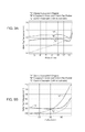
- FIGS. 7A-7D are graphs illustrating substrate temperature as a function of chord length tested at different slopes of the angled surface according to Implementations of the present disclosure.
- FIGS. 8A and 8B are graphs illustrating substrate temperature as a function of the radius of the substrate tested with two different susceptor designs according to Implementations of the present disclosure.
- FIGS. 9A and 9B are graphs illustrating substrate temperature as a function of the radius of the substrate tested with three different susceptor designs according to Implementations of the present disclosure.
- Implementations of the present disclosure generally relate to a susceptor for thermal processing of semiconductor substrates. Implementations disclosed can improve thermal uniformity across the surface of a substrate during processing by reducing a contacting surface area between the susceptor and the substrate. Reducing the contacting surface area between the susceptor and the substrate reduces the amount of heat that is transferred from the susceptor to the substrate by conduction during processing.
- the angled surface of the susceptor that is in contact with the substrate may have a plurality of cut-outs or tabs to provide azimuthal heat uniformity around the circumference of the susceptor.
- the susceptor may further provide a plurality of radial channels around the circumference of the susceptor to help venting of the heat or gas flow during processing. Details of the Implementations of the susceptor are described below.
- FIG. 1 illustrates a schematic sectional view of a conventional process chamber 100 with components in position for processing that may be benefit from Implementations of the present disclosure. It is contemplated that while a process chamber for epitaxial process is shown and described, the concept of the present disclosure is also applicable to other process chamber that is capable of providing a controlled thermal cycle that heats the substrate for processes such as, for example, thermal annealing, thermal cleaning, thermal chemical vapor deposition, thermal oxidation and thermal nitridation, regardless of whether the heating elements are provided at the top, bottom, or both of the process chamber.
- thermal annealing thermal cleaning
- thermal chemical vapor deposition thermal chemical vapor deposition
- thermal oxidation and thermal nitridation regardless of whether the heating elements are provided at the top, bottom, or both of the process chamber.
- the process chamber 100 and the associated hardware may be formed from one or more process-compatible materials, such as stainless steel, quartz (e.g., fused silica glass), SiC, CVD-coated SiC over graphite (30-200 microns), and combinations and alloys thereof, for example.
- the process chamber 100 may be used to process one or more substrates, including the deposition of a material on an upper surface of a substrate 108 .
- the process chamber 100 includes an array of radiant heating lamps 102 for heating, among other components, a back side 104 of a susceptor 106 disposed within the process chamber 100 .
- the susceptor 106 may be located within the process chamber 100 between an upper dome 128 and a lower dome 114 .
- an array of radiant heating lamps may be disposed over the upper dome 128 in addition to the array shown below the lower dome 114 .
- the susceptor 106 may be a disk-like susceptor, or may be a ring-like susceptor support with a central opening, which supports the substrate from the edge of the substrate to facilitate exposure of the substrate to the thermal radiation of the lamps 102 .
- the susceptor 106 is supported by a central shaft 132 , which may directly or indirectly support the susceptor 106 as shown in FIG. 1 .
- the upper dome 128 , the lower dome 114 , and a base ring 136 that is disposed between the upper dome 128 and lower dome 114 define an internal region of the process chamber 100 .
- the central portions of the upper dome 128 and of the lower dome 114 may be formed from an optically transparent material, such as quartz.
- the internal region of the process chamber 100 is generally divided into a process region 156 and a purge region 158 .
- the substrate 108 (not to scale) can be brought into the process chamber 100 through a loading port (not shown, obscured by the susceptor 106 ) and positioned on the susceptor 106 .
- the process chamber 100 also comprises a lamphead 145 , which supports the array of lamps 102 and cools the lamps 102 during and/or after processing.
- Each lamp 102 is coupled to an electricity distribution board (not shown), which supplies electricity to each lamp 102 .
- a preheat ring 167 may be optionally disposed around the susceptor 106 and surrounded by a liner assembly 163 .
- the preheat ring 167 prevents or reduces leakage of heat and or light noise from the lamps 102 to the device side 116 of the substrate 108 while providing a pre-heat zone for the process gases.
- the preheat ring 167 may be made from chemical vapor deposited (CVD) SiC, sintered graphite coated with SiC, grown SiC, opaque quartz, coated quartz, or any similar, suitable material that is resistant to chemical breakdown by process and purging gases.
- the liner assembly 163 is sized to be nested within or surrounded by an inner circumference of the base ring 136 .
- the liner assembly 163 shields the metallic walls of the process chamber 100 from the process gases used in processing. The metallic walls may react with the process gases and be damaged or introduce contamination into the process chamber 100 . While the liner assembly 163 is shown as a single body, in Implementations of the present disclosure, the liner assembly 163 may comprise one or more liners and other components.
- the process chamber 100 may also include one or more optical pyrometer(s) 118 , which measure temperatures within the process chamber 100 and on the surface of substrate 108 .
- a controller (not shown) controls electricity distribution from the electricity distribution board to the lamps 102 and flows of cooling fluids within the process chamber 100 .
- the controller controls temperatures within the process chamber by varying the electrical voltage from the electrical distribution board to the lamps 102 and by varying the flows of cooling fluids.
- a reflector 122 may be optionally placed outside the upper dome 128 to reflect infrared light radiating from the substrate 108 and upper dome 128 back into the process chamber 100 .
- the reflector 122 may be secured to the upper dome 128 using a clamp ring 130 .
- the reflector 122 may have one or more connection ports 126 connected to a cooling fluid source (not shown).
- the connection ports 126 may connect to one or more passages (not shown) within the reflector to allow cooling fluid (e.g., water) to circulate within the reflector 122 .
- the process chamber 100 comprises a process gas inlet 174 connected to a process gas source 172 .
- the process gas inlet 174 may be configured to direct process gas generally across the surface of the substrate 108 .
- the process chamber may also comprise a process gas outlet 178 located on the side of the process chamber 100 opposite the process gas inlet 174 .
- the process gas outlet 178 is coupled to a vacuum pump 180 .
- the process chamber 100 comprises a purge gas inlet 164 formed in the sidewall of the base ring 136 .
- a purge gas source 162 supplies purge gas to the purge gas inlet 164 .
- the process chamber 100 comprises the preheat ring 167
- the preheat ring 167 is disposed between the process gas inlet 174 and the purge gas inlet 164 .
- the process gas inlet 174 , purge gas inlet 164 , and process gas outlet 178 are shown for illustrative purposes, and the position, size, number of gas inlets and outlets, etc. may be adjusted to facilitate a uniform deposition of material on the substrate 108 .
- the susceptor 106 is shown in a position to allow processing of a substrate in the process chamber.
- the central shaft 132 , susceptor 106 , and arms 134 may be lowered by an actuator (not shown).
- a plurality of lift pins 105 pass through the susceptor 106 .
- Lowering the susceptor to a loading position below the processing position allows lift pins 105 to contact the lower dome 114 , pass through holes in the susceptor 106 and the central shaft 132 , and raise the substrate 108 from the susceptor 106 .
- a robot (not shown) then enters the process chamber 100 to engage and remove the substrate 108 though the loading port (not shown).
- the robot or another robot enters the process chamber through the loading port and places an unprocessed substrate on the susceptor 106 .
- the susceptor 106 then is raised to the processing position by the actuator to place the unprocessed substrate in position for processing.
- processing of a substrate 108 in the process chamber 100 comprises inserting the substrate through the loading port, placing the substrate 108 on the susceptor 106 , raising the susceptor 106 and substrate 108 to the processing position, heating the substrate 108 by the lamps 102 , flowing process gas 173 across the substrate 108 , and rotating the substrate 108 .
- the substrate may also be raised or lowered during processing.
- epitaxial processing in process chamber 100 comprises controlling the pressure within the process chamber 100 to be lower than atmospheric pressure. In some Implementations, pressure within the process chamber 100 is reduced to be between approximately 10 torr and 80 torr. In some Implementations, pressure within the process chamber 100 is reduced to be between approximately 80 torr and 300 torr.
- the vacuum pump 180 is activated to reduce the pressure of the process chamber 100 before and/or during processing.
- the process gas 173 is introduced into the process chamber 100 from one or more process gas inlets 174 , and exits the process chamber 100 through one or more process gas outlets 178 .
- the process gas 173 deposits one or more materials on the substrate 108 through thermal decomposition, for example, or other reactions. After depositing materials on the substrate 108 , effluent (i.e., waste gases) 175 are formed from the reactions. The effluent 175 exits the process chamber 100 through the process gas outlets 178 .
- the process chamber is purged of process gas 173 and effluent 175 by introduction of purge gas 165 (e.g., hydrogen or nitrogen) through the purge gas inlets 164 .
- Purge gas 165 may be introduced through the process gas inlets 174 instead of, or in addition to, the purge gas inlets 164 .
- the purge gas 175 exits the process chamber through the process gas outlets 178 .
- FIG. 2 illustrates a perspective view of an exemplary susceptor 200 that may be used in place of the susceptor 106 ( FIG. 1 ) according to Implementations of the disclosure.
- the susceptor 200 is a substantially annular plate divided into an inner region 204 , a first rim 206 surrounding and coupled to the inner region 204 , and a second rim 208 disposed between the inner region 204 and the first rim 206 .
- the inner region 204 may be slightly lower than a top surface 210 of the first rim 206 to form a recessed pocket 212 sized to receive the majority of the substrate.
- Susceptors such as susceptor 200
- the recessed pocket 212 thus prevents the substrate from slipping out during processing.
- the top surface of the recessed pocket 212 may be about 0.5 mm to about 2 mm below the top surface 210 of the first rim 206 .
- the height of the recessed pocket 212 is variable and is determined by the thickness of the substrate supported by the susceptor 200 .
- the inner region 204 is provided with a number of through-holes 202 , for example 3 through-holes, corresponding to the placement of the lift pins ( FIG. 1 ).
- the through-holes 202 allow the lift pins 105 to pass through the susceptor 200 to raise or lower the substrate from the susceptor 200 .
- the through-holes 202 may be arranged at 120 degree intervals in a circumferential direction.
- the second rim 208 may have an angled surface 214 , which serves as part of a supporting surface for a substrate.
- the angled surface 214 can reduce a contacting surface area between a substrate (not shown) and the susceptor 200 when the substrate is supported by the susceptor 200 .
- the angled surface 214 may be inclined with respect to a horizontal surface (e.g., top surface) of the inner region 204 .
- the angled surface 214 may be angled between about 2 degrees to about 20 degrees, such as about 6 degrees to about 15 degrees. Varying the slope or dimensions of the angled surface 214 can control the size of a gap between the bottom of the substrate and the upper surface of a recessed portion 218 ( FIG.
- the angle and location of the angled surface 214 can also be used to control a radial location corresponding to where the substrate can contact the angled surface 214 during processing.
- the angled surface 214 is a continuous surface around the circumference of the second rim 208 .
- the angled surface 214 may have two or more cut-outs, for example six (6) cut-outs, as shown in the implementation of FIG. 5A .
- FIG. 3A illustrates a partial cross-sectional view of a susceptor 300 that may be used in place of the susceptor 106 ( FIG. 1 ) according to Implementations of the disclosure.
- the cross-sectional view shows the angled surface 214 extending radially inward from an inner edge 216 of the first rim 206 toward the inner region 204 .
- a recessed portion 218 may be further provided between the angled surface 214 and an outer edge 220 of the inner region 204 .
- a top surface of the recessed portion 218 couples the angled surface 214 to the top surface of the recessed pocket 212 .
- the recessed portion 218 may be configured at an elevation slightly lower than the recessed pocket 212 .
- the top surface of the recessed portion 218 may be formed to a level of approximately 0.1 mm to about 0.2 mm below the top surface of the inner region 204 .
- the gap 222 between the bottom of the substrate 108 and the top surface of the recessed portion 218 may be between about 0.1 mm and about 1 mm, for example about 0.3 mm.
- the diameter of the inner region 204 may be about 290 mm.
- the outer edge 220 of the inner region 204 may be disposed at about 142 mm to about 150 mm, for example about 145 mm, measuring from the central axis of the inner region 204 .
- the recessed portion 218 abutting the outer edge 220 may be about 1.5 mm to about 4.5 mm in diameter, for example about 3 mm.
- the angled surface 214 can reduce a contacting surface area between a substrate 108 and the susceptor 300 when the substrate 108 is supported by the susceptor 300 .
- the substrate 108 may only contact the angled surface 214 during processing without contacting the inner region 204 or any other surface.
- a relatively steep angle such as between about 6 to about 15 degrees, for example 9 degrees, a smaller surface area of the substrate edge contacts the susceptor 300 during processing, which reduces the amount of conductive heat that can be transferred from the susceptor 300 to the substrate 108 .
- the angle and location of the angled surface 214 could be modified to achieve different thermal profiles during processing.
- the susceptor 300 may have one or more bumps, such as bumps 224 shown in FIG. 3B , extending from the top surface of the inner region 204 to prevent a sagging substrate from contacting the inner region 204 .
- the bumps or projections may be any suitable shape such as rectangular, rhombus, square, hemispherical, hexagonal, triangular protrusions or mixtures of differently shaped protrusions.
- the bumps 224 may be formed of the same material as the susceptor, or a different material, and may be made from silicon carbide, or graphite coated with silicon carbide or glassy carbon.
- the center of the substrate may sag below the edges of the substrate.
- the inner rim of the susceptors such as the inner region 204 , may be slightly concave (e.g., forming the recessed pocket 212 ) to prevent portions of an underside of a sagging substrate from contacting the susceptor during processing.
- the distance between the upper surface of the inner region 204 and the lower surface of the substrate is kept quite low, such as less than about 0.25 mm, for example about 0.15 mm.
- the bumps 224 can be used to support a sagging substrate, preventing contact between the inner region 204 and the substrate.
- the bumps 224 provide a contact surface area between the sagging substrate and the susceptor that is smaller than the surface area of the substrate that would contact the inner region 204 absent the bumps 224 .
- the bumps 224 may be evenly distributed around the center of the inner region 204 or at regions close to the edge of the inner region 204 . In some Implementations, to ensure adequate support of a sagging substrate there could always be at least one bump 224 on a side of the inner region 204 .
- the bumps 224 may be disposed at a radial distance of about 20 mm to about 145 mm, such as about 50 mm to about 143 mm, for example about 140 mm, measuring from the center axis of the inner region 204 .
- the bumps 224 may be about 0.4 mm to about 0.65 mm in diameter, for example about 0.56 mm in diameter.
- the bumps 224 may have a height of about 0.05 mm to about 0.12 mm, for example about 0.1 mm.
- the susceptor may be a wavy design including concentric annular ridges 352 surrounding the center of the inner region 204 , as the susceptor 350 shown in FIG. 3C .
- Each annular ridge 352 may have a different diameter.
- the susceptor may not provide the recessed portion 218 as shown in FIGS. 3A and 3B . In such a case, at least some of the annular ridges 352 may be located proximate an inner edge 262 of the angled surface 214 .
- the one or both of the annular ridges 352 and their respective upper surfaces are elevated structures relative to the top surface of the inner region 204 .
- the ridges 352 may also improve thermal uniformity when processing a substrate by increasing radiative surface area of the upper surface of the susceptor 160 .
- the annular ridges 352 may be made of the same material or a different material, which may be any of the same materials from which the susceptor is made. In some Implementations, some of the annular ridges 352 may be located within about 1 mm of the inner edge 262 , for example within about 0.5 mm of the inner edge 262 .
- the annular ridges 352 can reduce a contacting surface area between a substrate and the susceptor 350 when the substrate is supported by the susceptor 350 . It is contemplated that Implementations of FIG. 3C may be combined with any other Implementations disclosed in the present disclosure.
- FIG. 4A illustrates a top sectional view of a susceptor 400 that may be used in place of the susceptor 106 ( FIG. 1 ) according to Implementations of the disclosure.
- FIG. 4B illustrates an enlarged, partial top sectional view of the susceptor 400 shown in FIG. 4A .
- Implementations of FIGS. 4A and 4B are based on the Implementations of FIGS. 2 and 3A-3B .
- the susceptor 400 further includes a plurality of cut-outs 402 in the second rim 208 .
- the cut-outs 402 may be disposed in the angled surface 214 around the circumference of the susceptor 400 .
- cut-outs 402 improve thermal uniformity at the edges of the substrate because there are more gaps where the substrate is not contacting the susceptor 400 .
- these cut-outs 402 provide a reduced or minimum contact surface between the susceptor and the substrate, which helps prevent localized hotspots from forming along the edges of the substrate since the contacting surface area between the susceptor and the substrate is greatly reduced.
- the cut-outs 402 may be made by carving or sculpting a recess from an unpatterned susceptor surface using any suitable technique.
- More or less cut-outs 402 are contemplated. More cut-outs may provide higher thermal uniformity during processing by reducing the size of the individual surface areas on the susceptor 400 transferring heat to the substrate by conduction.
- the cut-outs 402 may be separated from one another at regular intervals in a circumferential direction. If 180 cut-outs were adapted, for example, each cut-out 402 may be separated azimuthally from two adjacent cut-outs by a 2 degree interval.
- the cut-outs may have a width of about 2 mm to about 10 mm, for example about 3 mm to about 8 mm.
- the cut-outs 402 may have any suitable shape such as arch-shaped, rectangular-shaped, square-shaped, round-shaped, V-shaped, U-shaped, or C-shaped cut-outs and their variations, or elongated shape of the above, or a combination thereof.
- FIGS. 4A and 4B illustrate one implementation where arch-shaped cut-outs are adapted.
- the susceptor 400 may optionally provide a plurality of venting channels 420 extending at a radial distance from the outer edge 220 of the inner region 204 towards the center of the inner region 204 .
- the venting channels 420 are configured to help gas flow or exhaust gases trapped in the recessed pocket 212 to the recessed portion 218 , and then into the internal region of the process chamber. Without venting channels 420 , gases may become trapped, for example, when the substrate is initially positioned on the susceptor 400 , during processing, or the like. If the gases remained trapped, for example, during a rapid pressure decrease in chamber pressure, the trapped gases may expand against the reduced chamber pressure causing the substrate to jump, shift, or otherwise move from its location on the susceptor.
- the venting channels 420 may be extended inwardly at a radial distance of about 30 mm to about 80 mm from the outer edge 220 of the inner region 204 .
- the venting channels 420 may be arranged at regular intervals around the circumference of the susceptor 400 .
- the venting channels 420 may be formed as vertical trenches or grooves cut into the surface of the susceptor 400 at the inner region 204 .
- the bottom surface of the venting channels 420 may be at the same elevation as the bottom surface of the cut-outs 402 .
- the venting channels 420 may be spaced apart from one another azimuthally by an angle of about 4 degrees to about 8 degrees, for example about 6 degrees.
- venting channels 420 may be cut to any suitable depth and/or length, and the number and/or spacing between venting channels 420 may be selected to enact rapid exhaust of gases from the recessed pocket 212 .
- the venting channels 420 may extend completely through the inner region 204 of the susceptor 400 .
- FIG. 4C illustrates the susceptor 400 according to other Implementations of the present disclosure.
- two or more different shapes of cut-outs as discussed above are formed in the angled surface 214 .
- a first group of cut-outs having a first shape and a second group of cut-outs having a second shape that is different from the first shape may be alternatingly arranged along the circumference of the susceptor 106 .
- Each group may contain two or more cut-outs of the same shape. In one example as shown in FIG.
- the cut-outs include a first group of arch-shaped cut-outs 430 and a second group of rectangular-shaped cut-outs 432 alternatingly arranged around the circumference of the susceptor 106 .
- two arch-shaped cut-outs 430 are sandwiched between rectangular-shaped cut-outs 432 , wherein the rectangular-shaped cut-outs 432 are generally in line with the venting channels 420 (i.e., corresponding to the radial location of the venting channels 420 along the circumference of the susceptor).
- the arch-shaped cut-outs may have a width of about 2 mm, and two arch-shaped cut-outs may be separated azimuthally from each other by a 2 degree interval.
- FIG. 4D illustrates the susceptor 400 according to another implementation of the present disclosure.
- the cut-outs 436 are all rectangular-shaped cut-outs arranged around the circumference of the susceptor 400 at regular intervals. Each of the cut-outs 436 may have a width of about 8 mm. In some aspects, the cut-outs 436 are in line with the venting channels 420 (i.e., corresponding to the radial location of the venting channels 420 along the circumference of the susceptor).
- FIG. 5A illustrates a perspective view of an exemplary susceptor 500 that may be used in place of the susceptor 106 ( FIG. 1 ) according to Implementations of the present disclosure.
- the susceptor 500 has a plurality of cut-outs 502 , for example about 2 to about 20 cut-outs. In one implementation as shown in FIG. 5A , six (6) wide cut-outs 502 are arranged within the second rim 208 around the circumference of the susceptor 500 .
- FIG. 5B illustrates an enlarged, partial top sectional view of the susceptor 500 shown in FIG. 5A according to Implementations of the present disclosure. As can be seen in FIG.
- a step 503 is formed at an interface between the second rim 208 and the first rim 206 .
- the step 503 connects the top surface 210 of the first rim 206 to the angled surface 214 .
- the step 503 may have a height of about 2 mm to about 3 mm to prevent a substrate (not shown) from slipping out during processing.
- the angled surface 214 couples the step 503 to the recessed portion 218 and provides a supporting surface for a substrate when the substrate is supported by the angled surface 214 .
- the cut-outs 502 are formed to have a sidewall 504 encircling a bottom surface 506 .
- the bottom surface 506 of the cut-out 502 is in parallel relationship to the top surface of the first rim 206 .
- the sidewalls 504 along the radial direction of the susceptor 500 are gradually decreased in thickness towards the recessed portion 218 .
- the sidewall 504 may gradually change in thickness of between about 0.55 mm and about 1.8 mm.
- each cut-out 502 may have a uniform thickness along the radial direction of the susceptor 500 .
- each of the cut-outs 502 (only two cut-outs are partially seen) has two rounded corners “C” proximate to the step 503 .
- the angled surface 214 sandwiched between two adjacent cut-outs 502 forms a T-shaped tab having a wide neck portion 508 at one end proximate to the first rim 206 , a tip portion 510 at another end opposing the wide neck portion 508 , and a narrow portion 512 connecting the wide neck portion 508 and the tip portion 510 .
- the number of the tabs may be between about 6 to about 360.
- the angled surface 214 or the T-shaped tab may have a thickness ranging between about 0.55 mm and about 1.8 mm. In some Implementations, the thickness of the T-shaped tab may be gradually changed along the radial direction from the first rim 206 towards the inner region 204 .
- the tip portion 510 is proximate to the inner region 204 and extends in the same direction from the wide neck portion 508 .
- the wide neck portion 508 is relatively wider than the tip portion 510 .
- the tip portion 510 is relatively wider than the narrow portion 512 .
- the narrow portion 512 of the angled surface 214 may be at a 2 degree downward slope towards the inner region 204 and forms a supporting surface for a substrate.
- the wide neck portion 508 may be about 1.6 mm to about 2.2 mm in width, measuring from the corners of two adjacent cut-outs having the greatest thickness.
- the tip portion may be about 1.2 mm to about 1.6 mm in width, measuring from the sidewalls of two adjacent cut-outs having the smallest thickness.
- the sidewall at the corners “C” of the cut-out 502 is about 0.75 mm to about 1.5 mm in thickness.
- the wide neck portion 508 is about 1.99 mm in width, and the tip portion 510 is about 1.42 mm in width.
- angled surface 214 forming a T-shaped tab any shape, such as arch-shaped, rectangular-shaped, square-shaped, round-shaped, V-shaped, U-shaped, or C-shaped taps and their variations, or elongated shape of the above, or a combination thereof is contemplated.
- the angled surface 214 may have a plurality of tabs having any of the shapes described herein, or the angled surface 214 may be in the form of a plurality of tabs having any of the shapes described herein.
- FIG. 6A illustrates a perspective view of a susceptor 600 that may be used in place of the susceptor 106 ( FIG. 1 ) according to another implementation of the present disclosure.
- the susceptor 600 has a plurality of cut-outs 602 formed in the second rim 208 . In one aspect, there are 180 cut-outs 602 arranged within the second rim 208 around the circumference of the susceptor 600 .
- FIG. 6B illustrates an enlarged, partial top sectional view of the susceptor 600 shown in FIG. 6A according to Implementations of the present disclosure.
- the cut-outs 602 formed in the angled surface 614 are elongated cut-outs extending along a radial direction of the susceptor 600 .
- the cut-outs are separated from each other by a tap 620 . Therefore, the taps 620 are formed in the angled surface 614 and may be spaced apart from one another at a regular interval around the circumference of the susceptor 600 .
- the cut-outs 602 are spaced apart from one another azimuthally by an angle of about 2 degrees. More or less number of cut-outs is contemplated. In some Implementations where 12 cut-outs are adapted, the cut-outs may be spaced apart from one another azimuthally by an angle of about 30 degrees. In some Implementations where 24 cut-outs are adapted, the cut-outs may be spaced apart from one another azimuthally by an angle of about 15 degrees. It is also contemplated that the cut-outs and/or the taps may have any suitable shape such as arch, rectangular, square, round, V-shaped, or their variations.
- the angled surface 614 may be at a 2 degree downward slope towards the inner region 204 and forms a supporting surface for a substrate.
- the width of the space 616 between two adjacent cut-outs 602 is about 2 mm to about 4 mm, for example about 3 mm.
- the sidewalls 604 along the radial direction of the susceptor 106 are gradually decreased in thickness towards the recessed portion 218 .
- the sidewall 604 may gradually change in thickness of between about 0.55 mm and about 1.8 mm.
- the sidewall at the corners “C” of the cut-out 602 is about 0.75 mm to about 1.5 mm in thickness.
- each cut-out 602 may have a uniform thickness along the radial direction of the susceptor 600 .
- FIGS. 7A-7D are graphs illustrating substrate temperature (° C.) as a function of chord length (maximum distance across a substrate) tested at different slopes of the angled surface according to Implementations of the present disclosure.
- the graphs represent the azimuthal temperature profile at substrate edges.
- FIG. 7A shows azimuthal temperature profile measured at 143 mm from the center of the substrate.
- FIG. 7B shows azimuthal temperature profile measured at 145 mm from the center of the substrate.
- FIG. 7C shows azimuthal temperature profile measured at 147 mm from the center of the substrate.
- FIG. 7D shows azimuthal temperature profile measured at 149 mm from the center of the substrate.
- the curve line “F” in FIGS. 7A-7D are obtained using the Implementations associated with FIG. 4C of the present disclosure.
- the curve line “F” in every tests shows a much flatter azimuthal temperature profile compared to other curve lines obtained by adapting the angled surface with greater slope angles. It has been proved that Implementations of the present disclosure are able to provide a lower azimuthal non-uniformity even at 149 mm measuring from the center of the substrate.
- FIGS. 8A and 8B are graphs illustrating substrate temperature (° C.) as a function of the radius of the substrate (mm) tested with two different susceptor designs according to Implementations of the present disclosure.
- the curve line “A” represents the substrate temperature profile measured at a susceptor adapting a flat susceptor design as discussed above with respect to FIGS. 3A and 3B , which has a substrate support surface angled at a 6 degree downward slope towards an inner rim of the susceptor, with a 0.15 mm gap between a top surface of the inner rim and a back surface of the substrate, and a 0.3 mm gap between a top surface of a recessed portion and the back surface of the substrate.
- the curve line “B” represents the substrate temperature profile measured at a susceptor adapting a wavy susceptor design as discussed above with respect to FIG. 3C , which has a substrate support surface angled at a 6 degree downward slope towards an inner rim of the susceptor, with concentric annular ridges surrounding the center of the inner rim. As can be seen, there is a temperature profile valley around 140 mm from the center of the susceptor, and both curve lines “A” and “B” show the substrate temperature profile is relatively flatter.
- FIGS. 9A and 9B are graphs illustrating substrate temperature (° C.) as a function of the radius of the substrate (mm) tested with three different susceptor designs according to Implementations of the present disclosure.
- the curve line “A” represents the substrate temperature profile measured at a susceptor adapting a flat susceptor design as discussed above with respect to FIGS. 3A and 3B .
- the curve line “B” represents the substrate temperature profile measured at a susceptor adapting a wavy susceptor design as discussed above with respect to FIG. 3C .
- the curve line “C” represents the substrate temperature profile measured at a susceptor adapting a conventional susceptor design having no annular ridges, no recessed portion, and cut-outs.
- the curve lines “A” and “B” show the substrate temperature variation for the wavy and flat susceptor designs according to Implementations of the present disclosure is only about 5 degrees as compared to curve line “C”.
- the susceptor Implementations described herein allow for more uniform temperature control of substrates during thermal processes, such as epitaxy.
- the temperature control is improved by reducing the surface area of the substrate contacting the susceptor, which reduces edge thermal peak and the amount of conductive heat transferred from the susceptor and the substrate.
- Conductive heat transfer between the susceptor and the substrate is more difficult to control than radiant heat transfer, the primary source of heat transfer between the susceptor and the substrate. Reducing the surface area of the substrate contacting the susceptor allows for a higher percentage of the heat transfer to be radiant heat resulting in improved temperature control and improved depositions on the substrate.
- the Implementations disclosed reduce the conductive heat transfer near the edge of the substrate by providing cut-outs around the circumference of the susceptor, such as cut-outs in the angled surface of the susceptor to which the substrate is contact with, to reduce the contacting surface area between the susceptor and the substrate.
- the Implementations disclosed also help gas flow or exhaust gases by including venting channels at regular intervals within the inner rim of the susceptor around the circumference of the susceptor. The combination of the cut-outs and venting channels prevent the possibility of substantial amounts of conductive heat transfer near the center and edge of the substrate during processing.
Landscapes
- Engineering & Computer Science (AREA)
- Physics & Mathematics (AREA)
- Condensed Matter Physics & Semiconductors (AREA)
- General Physics & Mathematics (AREA)
- Manufacturing & Machinery (AREA)
- Computer Hardware Design (AREA)
- Microelectronics & Electronic Packaging (AREA)
- Power Engineering (AREA)
- Chemical & Material Sciences (AREA)
- Health & Medical Sciences (AREA)
- Toxicology (AREA)
- General Chemical & Material Sciences (AREA)
- Chemical Kinetics & Catalysis (AREA)
- Materials Engineering (AREA)
- Mechanical Engineering (AREA)
- Metallurgy (AREA)
- Organic Chemistry (AREA)
- Chemical Vapour Deposition (AREA)
- Container, Conveyance, Adherence, Positioning, Of Wafer (AREA)
Priority Applications (5)
| Application Number | Priority Date | Filing Date | Title |
|---|---|---|---|
| US14/885,016 US10269614B2 (en) | 2014-11-12 | 2015-10-16 | Susceptor design to reduce edge thermal peak |
| CN201580061349.9A CN107004619B (zh) | 2014-11-12 | 2015-10-22 | 用以减少边缘热峰的基座设计 |
| KR1020177016028A KR102493889B1 (ko) | 2014-11-12 | 2015-10-22 | 에지 열 피크를 감소시키기 위한 신규 서셉터 설계 |
| PCT/US2015/056994 WO2016077051A1 (en) | 2014-11-12 | 2015-10-22 | New susceptor design to reduce edge thermal peak |
| SG11201703351PA SG11201703351PA (en) | 2014-11-12 | 2015-10-22 | New susceptor design to reduce edge thermal peak |
Applications Claiming Priority (3)
| Application Number | Priority Date | Filing Date | Title |
|---|---|---|---|
| US201462078782P | 2014-11-12 | 2014-11-12 | |
| US201462084821P | 2014-11-26 | 2014-11-26 | |
| US14/885,016 US10269614B2 (en) | 2014-11-12 | 2015-10-16 | Susceptor design to reduce edge thermal peak |
Publications (2)
| Publication Number | Publication Date |
|---|---|
| US20160133504A1 US20160133504A1 (en) | 2016-05-12 |
| US10269614B2 true US10269614B2 (en) | 2019-04-23 |
Family
ID=55912818
Family Applications (1)
| Application Number | Title | Priority Date | Filing Date |
|---|---|---|---|
| US14/885,016 Active 2037-05-14 US10269614B2 (en) | 2014-11-12 | 2015-10-16 | Susceptor design to reduce edge thermal peak |
Country Status (6)
| Country | Link |
|---|---|
| US (1) | US10269614B2 (ko) |
| KR (1) | KR102493889B1 (ko) |
| CN (1) | CN107004619B (ko) |
| SG (1) | SG11201703351PA (ko) |
| TW (1) | TWI684236B (ko) |
| WO (1) | WO2016077051A1 (ko) |
Cited By (1)
| Publication number | Priority date | Publication date | Assignee | Title |
|---|---|---|---|---|
| US20210125853A1 (en) * | 2019-10-24 | 2021-04-29 | Asm Ip Holding B.V. | Susceptor for semiconductor substrate processing |
Families Citing this family (206)
| Publication number | Priority date | Publication date | Assignee | Title |
|---|---|---|---|---|
| US20130023129A1 (en) | 2011-07-20 | 2013-01-24 | Asm America, Inc. | Pressure transmitter for a semiconductor processing environment |
| US10714315B2 (en) | 2012-10-12 | 2020-07-14 | Asm Ip Holdings B.V. | Semiconductor reaction chamber showerhead |
| US20160376700A1 (en) | 2013-02-01 | 2016-12-29 | Asm Ip Holding B.V. | System for treatment of deposition reactor |
| US9799548B2 (en) * | 2013-03-15 | 2017-10-24 | Applied Materials, Inc. | Susceptors for enhanced process uniformity and reduced substrate slippage |
| WO2015040907A1 (ja) * | 2013-09-17 | 2015-03-26 | 株式会社村田製作所 | 垂直共振器型面発光レーザの製造方法 |
| SG11201608905XA (en) * | 2014-05-21 | 2016-12-29 | Applied Materials Inc | Thermal processing susceptor |
| US10941490B2 (en) | 2014-10-07 | 2021-03-09 | Asm Ip Holding B.V. | Multiple temperature range susceptor, assembly, reactor and system including the susceptor, and methods of using the same |
| KR20170102020A (ko) * | 2015-01-23 | 2017-09-06 | 어플라이드 머티어리얼스, 인코포레이티드 | 웨이퍼 내의 퇴적 계곡들을 제거하기 위한 신규한 서셉터 설계 |
| US10276355B2 (en) | 2015-03-12 | 2019-04-30 | Asm Ip Holding B.V. | Multi-zone reactor, system including the reactor, and method of using the same |
| US10458018B2 (en) | 2015-06-26 | 2019-10-29 | Asm Ip Holding B.V. | Structures including metal carbide material, devices including the structures, and methods of forming same |
| US10599049B2 (en) * | 2015-09-28 | 2020-03-24 | Asml Netherlands B.V. | Substrate holder, a lithographic apparatus and method of manufacturing devices |
| US10211308B2 (en) | 2015-10-21 | 2019-02-19 | Asm Ip Holding B.V. | NbMC layers |
| US11139308B2 (en) | 2015-12-29 | 2021-10-05 | Asm Ip Holding B.V. | Atomic layer deposition of III-V compounds to form V-NAND devices |
| US10529554B2 (en) | 2016-02-19 | 2020-01-07 | Asm Ip Holding B.V. | Method for forming silicon nitride film selectively on sidewalls or flat surfaces of trenches |
| US11453943B2 (en) | 2016-05-25 | 2022-09-27 | Asm Ip Holding B.V. | Method for forming carbon-containing silicon/metal oxide or nitride film by ALD using silicon precursor and hydrocarbon precursor |
| KR102361352B1 (ko) * | 2016-06-14 | 2022-02-10 | 신에쯔 세끼에이 가부시키가이샤 | 노출 면적 증대 석영 유리 부재 및 그 제조 방법 및 멀티 외주 절삭 날 |
| US10612137B2 (en) | 2016-07-08 | 2020-04-07 | Asm Ip Holdings B.V. | Organic reactants for atomic layer deposition |
| US9859151B1 (en) | 2016-07-08 | 2018-01-02 | Asm Ip Holding B.V. | Selective film deposition method to form air gaps |
| US10840114B1 (en) * | 2016-07-26 | 2020-11-17 | Raytheon Company | Rapid thermal anneal apparatus and method |
| US9812320B1 (en) | 2016-07-28 | 2017-11-07 | Asm Ip Holding B.V. | Method and apparatus for filling a gap |
| US9887082B1 (en) | 2016-07-28 | 2018-02-06 | Asm Ip Holding B.V. | Method and apparatus for filling a gap |
| JP2018026503A (ja) * | 2016-08-12 | 2018-02-15 | 株式会社Sumco | サセプタ、エピタキシャル成長装置、及びエピタキシャルウェーハの製造方法 |
| JP6587354B2 (ja) * | 2016-10-06 | 2019-10-09 | クアーズテック株式会社 | サセプタ |
| US11532757B2 (en) | 2016-10-27 | 2022-12-20 | Asm Ip Holding B.V. | Deposition of charge trapping layers |
| US10714350B2 (en) | 2016-11-01 | 2020-07-14 | ASM IP Holdings, B.V. | Methods for forming a transition metal niobium nitride film on a substrate by atomic layer deposition and related semiconductor device structures |
| KR102546317B1 (ko) | 2016-11-15 | 2023-06-21 | 에이에스엠 아이피 홀딩 비.브이. | 기체 공급 유닛 및 이를 포함하는 기판 처리 장치 |
| KR20180068582A (ko) | 2016-12-14 | 2018-06-22 | 에이에스엠 아이피 홀딩 비.브이. | 기판 처리 장치 |
| US11581186B2 (en) | 2016-12-15 | 2023-02-14 | Asm Ip Holding B.V. | Sequential infiltration synthesis apparatus |
| US11447861B2 (en) | 2016-12-15 | 2022-09-20 | Asm Ip Holding B.V. | Sequential infiltration synthesis apparatus and a method of forming a patterned structure |
| US10655224B2 (en) * | 2016-12-20 | 2020-05-19 | Lam Research Corporation | Conical wafer centering and holding device for semiconductor processing |
| US10269558B2 (en) | 2016-12-22 | 2019-04-23 | Asm Ip Holding B.V. | Method of forming a structure on a substrate |
| US11390950B2 (en) | 2017-01-10 | 2022-07-19 | Asm Ip Holding B.V. | Reactor system and method to reduce residue buildup during a film deposition process |
| US10468261B2 (en) | 2017-02-15 | 2019-11-05 | Asm Ip Holding B.V. | Methods for forming a metallic film on a substrate by cyclical deposition and related semiconductor device structures |
| US10770286B2 (en) | 2017-05-08 | 2020-09-08 | Asm Ip Holdings B.V. | Methods for selectively forming a silicon nitride film on a substrate and related semiconductor device structures |
| US20180334746A1 (en) * | 2017-05-22 | 2018-11-22 | Lam Research Corporation | Wafer Edge Contact Hardware and Methods to Eliminate Deposition at Wafer Backside Edge and Notch |
| US11306395B2 (en) | 2017-06-28 | 2022-04-19 | Asm Ip Holding B.V. | Methods for depositing a transition metal nitride film on a substrate by atomic layer deposition and related deposition apparatus |
| KR20190009245A (ko) | 2017-07-18 | 2019-01-28 | 에이에스엠 아이피 홀딩 비.브이. | 반도체 소자 구조물 형성 방법 및 관련된 반도체 소자 구조물 |
| US11374112B2 (en) | 2017-07-19 | 2022-06-28 | Asm Ip Holding B.V. | Method for depositing a group IV semiconductor and related semiconductor device structures |
| US10590535B2 (en) | 2017-07-26 | 2020-03-17 | Asm Ip Holdings B.V. | Chemical treatment, deposition and/or infiltration apparatus and method for using the same |
| US10692741B2 (en) | 2017-08-08 | 2020-06-23 | Asm Ip Holdings B.V. | Radiation shield |
| US10770336B2 (en) | 2017-08-08 | 2020-09-08 | Asm Ip Holding B.V. | Substrate lift mechanism and reactor including same |
| US11769682B2 (en) | 2017-08-09 | 2023-09-26 | Asm Ip Holding B.V. | Storage apparatus for storing cassettes for substrates and processing apparatus equipped therewith |
| US11830730B2 (en) | 2017-08-29 | 2023-11-28 | Asm Ip Holding B.V. | Layer forming method and apparatus |
| US11295980B2 (en) | 2017-08-30 | 2022-04-05 | Asm Ip Holding B.V. | Methods for depositing a molybdenum metal film over a dielectric surface of a substrate by a cyclical deposition process and related semiconductor device structures |
| US10658205B2 (en) | 2017-09-28 | 2020-05-19 | Asm Ip Holdings B.V. | Chemical dispensing apparatus and methods for dispensing a chemical to a reaction chamber |
| KR102597978B1 (ko) | 2017-11-27 | 2023-11-06 | 에이에스엠 아이피 홀딩 비.브이. | 배치 퍼니스와 함께 사용하기 위한 웨이퍼 카세트를 보관하기 위한 보관 장치 |
| US11639811B2 (en) | 2017-11-27 | 2023-05-02 | Asm Ip Holding B.V. | Apparatus including a clean mini environment |
| US10872771B2 (en) | 2018-01-16 | 2020-12-22 | Asm Ip Holding B. V. | Method for depositing a material film on a substrate within a reaction chamber by a cyclical deposition process and related device structures |
| US11482412B2 (en) | 2018-01-19 | 2022-10-25 | Asm Ip Holding B.V. | Method for depositing a gap-fill layer by plasma-assisted deposition |
| TW202325889A (zh) | 2018-01-19 | 2023-07-01 | 荷蘭商Asm 智慧財產控股公司 | 沈積方法 |
| US11081345B2 (en) | 2018-02-06 | 2021-08-03 | Asm Ip Holding B.V. | Method of post-deposition treatment for silicon oxide film |
| US10896820B2 (en) | 2018-02-14 | 2021-01-19 | Asm Ip Holding B.V. | Method for depositing a ruthenium-containing film on a substrate by a cyclical deposition process |
| WO2019158960A1 (en) | 2018-02-14 | 2019-08-22 | Asm Ip Holding B.V. | A method for depositing a ruthenium-containing film on a substrate by a cyclical deposition process |
| KR102636427B1 (ko) | 2018-02-20 | 2024-02-13 | 에이에스엠 아이피 홀딩 비.브이. | 기판 처리 방법 및 장치 |
| US10975470B2 (en) | 2018-02-23 | 2021-04-13 | Asm Ip Holding B.V. | Apparatus for detecting or monitoring for a chemical precursor in a high temperature environment |
| US11473195B2 (en) | 2018-03-01 | 2022-10-18 | Asm Ip Holding B.V. | Semiconductor processing apparatus and a method for processing a substrate |
| US11629406B2 (en) | 2018-03-09 | 2023-04-18 | Asm Ip Holding B.V. | Semiconductor processing apparatus comprising one or more pyrometers for measuring a temperature of a substrate during transfer of the substrate |
| KR102646467B1 (ko) | 2018-03-27 | 2024-03-11 | 에이에스엠 아이피 홀딩 비.브이. | 기판 상에 전극을 형성하는 방법 및 전극을 포함하는 반도체 소자 구조 |
| US11230766B2 (en) | 2018-03-29 | 2022-01-25 | Asm Ip Holding B.V. | Substrate processing apparatus and method |
| TWI811348B (zh) | 2018-05-08 | 2023-08-11 | 荷蘭商Asm 智慧財產控股公司 | 藉由循環沉積製程於基板上沉積氧化物膜之方法及相關裝置結構 |
| KR102596988B1 (ko) | 2018-05-28 | 2023-10-31 | 에이에스엠 아이피 홀딩 비.브이. | 기판 처리 방법 및 그에 의해 제조된 장치 |
| US11270899B2 (en) | 2018-06-04 | 2022-03-08 | Asm Ip Holding B.V. | Wafer handling chamber with moisture reduction |
| US11718913B2 (en) | 2018-06-04 | 2023-08-08 | Asm Ip Holding B.V. | Gas distribution system and reactor system including same |
| US11286562B2 (en) | 2018-06-08 | 2022-03-29 | Asm Ip Holding B.V. | Gas-phase chemical reactor and method of using same |
| US10797133B2 (en) | 2018-06-21 | 2020-10-06 | Asm Ip Holding B.V. | Method for depositing a phosphorus doped silicon arsenide film and related semiconductor device structures |
| KR102568797B1 (ko) | 2018-06-21 | 2023-08-21 | 에이에스엠 아이피 홀딩 비.브이. | 기판 처리 시스템 |
| CN112292477A (zh) | 2018-06-27 | 2021-01-29 | Asm Ip私人控股有限公司 | 用于形成含金属的材料的循环沉积方法及包含含金属的材料的膜和结构 |
| JP2021529254A (ja) | 2018-06-27 | 2021-10-28 | エーエスエム・アイピー・ホールディング・ベー・フェー | 金属含有材料ならびに金属含有材料を含む膜および構造体を形成するための周期的堆積方法 |
| US10612136B2 (en) | 2018-06-29 | 2020-04-07 | ASM IP Holding, B.V. | Temperature-controlled flange and reactor system including same |
| US10755922B2 (en) | 2018-07-03 | 2020-08-25 | Asm Ip Holding B.V. | Method for depositing silicon-free carbon-containing film as gap-fill layer by pulse plasma-assisted deposition |
| US10388513B1 (en) | 2018-07-03 | 2019-08-20 | Asm Ip Holding B.V. | Method for depositing silicon-free carbon-containing film as gap-fill layer by pulse plasma-assisted deposition |
| US11430674B2 (en) | 2018-08-22 | 2022-08-30 | Asm Ip Holding B.V. | Sensor array, apparatus for dispensing a vapor phase reactant to a reaction chamber and related methods |
| US11024523B2 (en) | 2018-09-11 | 2021-06-01 | Asm Ip Holding B.V. | Substrate processing apparatus and method |
| KR20200030162A (ko) | 2018-09-11 | 2020-03-20 | 에이에스엠 아이피 홀딩 비.브이. | 박막 증착 방법 |
| CN110970344A (zh) | 2018-10-01 | 2020-04-07 | Asm Ip控股有限公司 | 衬底保持设备、包含所述设备的系统及其使用方法 |
| US11232963B2 (en) | 2018-10-03 | 2022-01-25 | Asm Ip Holding B.V. | Substrate processing apparatus and method |
| KR102592699B1 (ko) | 2018-10-08 | 2023-10-23 | 에이에스엠 아이피 홀딩 비.브이. | 기판 지지 유닛 및 이를 포함하는 박막 증착 장치와 기판 처리 장치 |
| KR102605121B1 (ko) | 2018-10-19 | 2023-11-23 | 에이에스엠 아이피 홀딩 비.브이. | 기판 처리 장치 및 기판 처리 방법 |
| KR102546322B1 (ko) | 2018-10-19 | 2023-06-21 | 에이에스엠 아이피 홀딩 비.브이. | 기판 처리 장치 및 기판 처리 방법 |
| US11087997B2 (en) | 2018-10-31 | 2021-08-10 | Asm Ip Holding B.V. | Substrate processing apparatus for processing substrates |
| KR20200051105A (ko) | 2018-11-02 | 2020-05-13 | 에이에스엠 아이피 홀딩 비.브이. | 기판 지지 유닛 및 이를 포함하는 기판 처리 장치 |
| US11572620B2 (en) | 2018-11-06 | 2023-02-07 | Asm Ip Holding B.V. | Methods for selectively depositing an amorphous silicon film on a substrate |
| US10818758B2 (en) | 2018-11-16 | 2020-10-27 | Asm Ip Holding B.V. | Methods for forming a metal silicate film on a substrate in a reaction chamber and related semiconductor device structures |
| US11217444B2 (en) | 2018-11-30 | 2022-01-04 | Asm Ip Holding B.V. | Method for forming an ultraviolet radiation responsive metal oxide-containing film |
| KR20210088723A (ko) | 2018-12-03 | 2021-07-14 | 어플라이드 머티어리얼스, 인코포레이티드 | 척킹 및 아크 발생 성능이 개선된 정전 척 설계 |
| KR102636428B1 (ko) | 2018-12-04 | 2024-02-13 | 에이에스엠 아이피 홀딩 비.브이. | 기판 처리 장치를 세정하는 방법 |
| US11158513B2 (en) | 2018-12-13 | 2021-10-26 | Asm Ip Holding B.V. | Methods for forming a rhenium-containing film on a substrate by a cyclical deposition process and related semiconductor device structures |
| JP2020096183A (ja) | 2018-12-14 | 2020-06-18 | エーエスエム・アイピー・ホールディング・ベー・フェー | 窒化ガリウムの選択的堆積を用いてデバイス構造体を形成する方法及びそのためのシステム |
| CN109594063A (zh) * | 2018-12-27 | 2019-04-09 | 西安奕斯伟硅片技术有限公司 | 一种外延反应设备 |
| CN111446185A (zh) * | 2019-01-17 | 2020-07-24 | Asm Ip 控股有限公司 | 通风基座 |
| USD920936S1 (en) | 2019-01-17 | 2021-06-01 | Asm Ip Holding B.V. | Higher temperature vented susceptor |
| TWI819180B (zh) | 2019-01-17 | 2023-10-21 | 荷蘭商Asm 智慧財產控股公司 | 藉由循環沈積製程於基板上形成含過渡金屬膜之方法 |
| KR20200091543A (ko) | 2019-01-22 | 2020-07-31 | 에이에스엠 아이피 홀딩 비.브이. | 기판 처리 장치 |
| JP2020136677A (ja) | 2019-02-20 | 2020-08-31 | エーエスエム・アイピー・ホールディング・ベー・フェー | 基材表面内に形成された凹部を充填するための周期的堆積方法および装置 |
| KR102626263B1 (ko) | 2019-02-20 | 2024-01-16 | 에이에스엠 아이피 홀딩 비.브이. | 처리 단계를 포함하는 주기적 증착 방법 및 이를 위한 장치 |
| KR102638425B1 (ko) | 2019-02-20 | 2024-02-21 | 에이에스엠 아이피 홀딩 비.브이. | 기판 표면 내에 형성된 오목부를 충진하기 위한 방법 및 장치 |
| US11482533B2 (en) | 2019-02-20 | 2022-10-25 | Asm Ip Holding B.V. | Apparatus and methods for plug fill deposition in 3-D NAND applications |
| JP2020133004A (ja) | 2019-02-22 | 2020-08-31 | エーエスエム・アイピー・ホールディング・ベー・フェー | 基材を処理するための基材処理装置および方法 |
| KR20200108242A (ko) | 2019-03-08 | 2020-09-17 | 에이에스엠 아이피 홀딩 비.브이. | 실리콘 질화물 층을 선택적으로 증착하는 방법, 및 선택적으로 증착된 실리콘 질화물 층을 포함하는 구조체 |
| US11742198B2 (en) | 2019-03-08 | 2023-08-29 | Asm Ip Holding B.V. | Structure including SiOCN layer and method of forming same |
| CN113597667A (zh) * | 2019-03-18 | 2021-11-02 | 爱思开矽得荣株式会社 | 用于制造半导体的基座和设备 |
| JP2020167398A (ja) | 2019-03-28 | 2020-10-08 | エーエスエム・アイピー・ホールディング・ベー・フェー | ドアオープナーおよびドアオープナーが提供される基材処理装置 |
| KR20200116855A (ko) | 2019-04-01 | 2020-10-13 | 에이에스엠 아이피 홀딩 비.브이. | 반도체 소자를 제조하는 방법 |
| US11447864B2 (en) | 2019-04-19 | 2022-09-20 | Asm Ip Holding B.V. | Layer forming method and apparatus |
| KR20200125453A (ko) | 2019-04-24 | 2020-11-04 | 에이에스엠 아이피 홀딩 비.브이. | 기상 반응기 시스템 및 이를 사용하는 방법 |
| KR20200130118A (ko) | 2019-05-07 | 2020-11-18 | 에이에스엠 아이피 홀딩 비.브이. | 비정질 탄소 중합체 막을 개질하는 방법 |
| KR20200130121A (ko) | 2019-05-07 | 2020-11-18 | 에이에스엠 아이피 홀딩 비.브이. | 딥 튜브가 있는 화학물질 공급원 용기 |
| KR20200130652A (ko) | 2019-05-10 | 2020-11-19 | 에이에스엠 아이피 홀딩 비.브이. | 표면 상에 재료를 증착하는 방법 및 본 방법에 따라 형성된 구조 |
| JP2020188255A (ja) | 2019-05-16 | 2020-11-19 | エーエスエム アイピー ホールディング ビー.ブイ. | ウェハボートハンドリング装置、縦型バッチ炉および方法 |
| USD947913S1 (en) | 2019-05-17 | 2022-04-05 | Asm Ip Holding B.V. | Susceptor shaft |
| USD975665S1 (en) | 2019-05-17 | 2023-01-17 | Asm Ip Holding B.V. | Susceptor shaft |
| TW202110587A (zh) | 2019-05-22 | 2021-03-16 | 荷蘭商Asm Ip 控股公司 | 工件基座主體及用於沖洗工件基座的方法 |
| KR20200141002A (ko) | 2019-06-06 | 2020-12-17 | 에이에스엠 아이피 홀딩 비.브이. | 배기 가스 분석을 포함한 기상 반응기 시스템을 사용하는 방법 |
| KR20200143254A (ko) | 2019-06-11 | 2020-12-23 | 에이에스엠 아이피 홀딩 비.브이. | 개질 가스를 사용하여 전자 구조를 형성하는 방법, 상기 방법을 수행하기 위한 시스템, 및 상기 방법을 사용하여 형성되는 구조 |
| USD944946S1 (en) | 2019-06-14 | 2022-03-01 | Asm Ip Holding B.V. | Shower plate |
| KR20210005515A (ko) | 2019-07-03 | 2021-01-14 | 에이에스엠 아이피 홀딩 비.브이. | 기판 처리 장치용 온도 제어 조립체 및 이를 사용하는 방법 |
| JP2021015791A (ja) | 2019-07-09 | 2021-02-12 | エーエスエム アイピー ホールディング ビー.ブイ. | 同軸導波管を用いたプラズマ装置、基板処理方法 |
| CN112216646A (zh) | 2019-07-10 | 2021-01-12 | Asm Ip私人控股有限公司 | 基板支撑组件及包括其的基板处理装置 |
| KR20210010307A (ko) | 2019-07-16 | 2021-01-27 | 에이에스엠 아이피 홀딩 비.브이. | 기판 처리 장치 |
| KR20210010820A (ko) | 2019-07-17 | 2021-01-28 | 에이에스엠 아이피 홀딩 비.브이. | 실리콘 게르마늄 구조를 형성하는 방법 |
| KR20210010816A (ko) | 2019-07-17 | 2021-01-28 | 에이에스엠 아이피 홀딩 비.브이. | 라디칼 보조 점화 플라즈마 시스템 및 방법 |
| US11643724B2 (en) | 2019-07-18 | 2023-05-09 | Asm Ip Holding B.V. | Method of forming structures using a neutral beam |
| CN112242296A (zh) | 2019-07-19 | 2021-01-19 | Asm Ip私人控股有限公司 | 形成拓扑受控的无定形碳聚合物膜的方法 |
| TW202113936A (zh) | 2019-07-29 | 2021-04-01 | 荷蘭商Asm Ip私人控股有限公司 | 用於利用n型摻雜物及/或替代摻雜物選擇性沉積以達成高摻雜物併入之方法 |
| CN112309900A (zh) | 2019-07-30 | 2021-02-02 | Asm Ip私人控股有限公司 | 基板处理设备 |
| CN112309899A (zh) | 2019-07-30 | 2021-02-02 | Asm Ip私人控股有限公司 | 基板处理设备 |
| US11587815B2 (en) | 2019-07-31 | 2023-02-21 | Asm Ip Holding B.V. | Vertical batch furnace assembly |
| US11227782B2 (en) | 2019-07-31 | 2022-01-18 | Asm Ip Holding B.V. | Vertical batch furnace assembly |
| US11587814B2 (en) | 2019-07-31 | 2023-02-21 | Asm Ip Holding B.V. | Vertical batch furnace assembly |
| CN110429050B (zh) * | 2019-08-05 | 2022-02-08 | 西安奕斯伟材料科技有限公司 | 一种外延生长基座 |
| CN112323048B (zh) | 2019-08-05 | 2024-02-09 | Asm Ip私人控股有限公司 | 用于化学源容器的液位传感器 |
| USD965044S1 (en) | 2019-08-19 | 2022-09-27 | Asm Ip Holding B.V. | Susceptor shaft |
| USD965524S1 (en) | 2019-08-19 | 2022-10-04 | Asm Ip Holding B.V. | Susceptor support |
| JP2021031769A (ja) | 2019-08-21 | 2021-03-01 | エーエスエム アイピー ホールディング ビー.ブイ. | 成膜原料混合ガス生成装置及び成膜装置 |
| USD940837S1 (en) | 2019-08-22 | 2022-01-11 | Asm Ip Holding B.V. | Electrode |
| KR20210024423A (ko) | 2019-08-22 | 2021-03-05 | 에이에스엠 아이피 홀딩 비.브이. | 홀을 구비한 구조체를 형성하기 위한 방법 |
| USD949319S1 (en) | 2019-08-22 | 2022-04-19 | Asm Ip Holding B.V. | Exhaust duct |
| USD979506S1 (en) | 2019-08-22 | 2023-02-28 | Asm Ip Holding B.V. | Insulator |
| KR20210024420A (ko) | 2019-08-23 | 2021-03-05 | 에이에스엠 아이피 홀딩 비.브이. | 비스(디에틸아미노)실란을 사용하여 peald에 의해 개선된 품질을 갖는 실리콘 산화물 막을 증착하기 위한 방법 |
| US11286558B2 (en) | 2019-08-23 | 2022-03-29 | Asm Ip Holding B.V. | Methods for depositing a molybdenum nitride film on a surface of a substrate by a cyclical deposition process and related semiconductor device structures including a molybdenum nitride film |
| IT201900015416A1 (it) * | 2019-09-03 | 2021-03-03 | St Microelectronics Srl | Apparecchio per la crescita di una fetta di materiale semiconduttore, in particolare di carburo di silicio, e procedimento di fabbricazione associato |
| KR20210029090A (ko) | 2019-09-04 | 2021-03-15 | 에이에스엠 아이피 홀딩 비.브이. | 희생 캡핑 층을 이용한 선택적 증착 방법 |
| KR20210029663A (ko) | 2019-09-05 | 2021-03-16 | 에이에스엠 아이피 홀딩 비.브이. | 기판 처리 장치 |
| US11562901B2 (en) | 2019-09-25 | 2023-01-24 | Asm Ip Holding B.V. | Substrate processing method |
| CN112593212B (zh) | 2019-10-02 | 2023-12-22 | Asm Ip私人控股有限公司 | 通过循环等离子体增强沉积工艺形成拓扑选择性氧化硅膜的方法 |
| TW202129060A (zh) | 2019-10-08 | 2021-08-01 | 荷蘭商Asm Ip控股公司 | 基板處理裝置、及基板處理方法 |
| TW202115273A (zh) | 2019-10-10 | 2021-04-16 | 荷蘭商Asm Ip私人控股有限公司 | 形成光阻底層之方法及包括光阻底層之結構 |
| KR20210045930A (ko) | 2019-10-16 | 2021-04-27 | 에이에스엠 아이피 홀딩 비.브이. | 실리콘 산화물의 토폴로지-선택적 막의 형성 방법 |
| US11637014B2 (en) | 2019-10-17 | 2023-04-25 | Asm Ip Holding B.V. | Methods for selective deposition of doped semiconductor material |
| KR20210047808A (ko) | 2019-10-21 | 2021-04-30 | 에이에스엠 아이피 홀딩 비.브이. | 막을 선택적으로 에칭하기 위한 장치 및 방법 |
| US11646205B2 (en) | 2019-10-29 | 2023-05-09 | Asm Ip Holding B.V. | Methods of selectively forming n-type doped material on a surface, systems for selectively forming n-type doped material, and structures formed using same |
| KR20210054983A (ko) | 2019-11-05 | 2021-05-14 | 에이에스엠 아이피 홀딩 비.브이. | 도핑된 반도체 층을 갖는 구조체 및 이를 형성하기 위한 방법 및 시스템 |
| US11501968B2 (en) | 2019-11-15 | 2022-11-15 | Asm Ip Holding B.V. | Method for providing a semiconductor device with silicon filled gaps |
| KR20210062561A (ko) | 2019-11-20 | 2021-05-31 | 에이에스엠 아이피 홀딩 비.브이. | 기판의 표면 상에 탄소 함유 물질을 증착하는 방법, 상기 방법을 사용하여 형성된 구조물, 및 상기 구조물을 형성하기 위한 시스템 |
| CN112951697A (zh) | 2019-11-26 | 2021-06-11 | Asm Ip私人控股有限公司 | 基板处理设备 |
| US11450529B2 (en) | 2019-11-26 | 2022-09-20 | Asm Ip Holding B.V. | Methods for selectively forming a target film on a substrate comprising a first dielectric surface and a second metallic surface |
| CN112885692A (zh) | 2019-11-29 | 2021-06-01 | Asm Ip私人控股有限公司 | 基板处理设备 |
| CN112885693A (zh) | 2019-11-29 | 2021-06-01 | Asm Ip私人控股有限公司 | 基板处理设备 |
| JP2021090042A (ja) | 2019-12-02 | 2021-06-10 | エーエスエム アイピー ホールディング ビー.ブイ. | 基板処理装置、基板処理方法 |
| KR20210070898A (ko) | 2019-12-04 | 2021-06-15 | 에이에스엠 아이피 홀딩 비.브이. | 기판 처리 장치 |
| JP2021097227A (ja) | 2019-12-17 | 2021-06-24 | エーエスエム・アイピー・ホールディング・ベー・フェー | 窒化バナジウム層および窒化バナジウム層を含む構造体を形成する方法 |
| US11527403B2 (en) | 2019-12-19 | 2022-12-13 | Asm Ip Holding B.V. | Methods for filling a gap feature on a substrate surface and related semiconductor structures |
| JP2021109175A (ja) | 2020-01-06 | 2021-08-02 | エーエスエム・アイピー・ホールディング・ベー・フェー | ガス供給アセンブリ、その構成要素、およびこれを含む反応器システム |
| KR20210095050A (ko) | 2020-01-20 | 2021-07-30 | 에이에스엠 아이피 홀딩 비.브이. | 박막 형성 방법 및 박막 표면 개질 방법 |
| TW202130846A (zh) | 2020-02-03 | 2021-08-16 | 荷蘭商Asm Ip私人控股有限公司 | 形成包括釩或銦層的結構之方法 |
| TW202146882A (zh) | 2020-02-04 | 2021-12-16 | 荷蘭商Asm Ip私人控股有限公司 | 驗證一物品之方法、用於驗證一物品之設備、及用於驗證一反應室之系統 |
| US11776846B2 (en) | 2020-02-07 | 2023-10-03 | Asm Ip Holding B.V. | Methods for depositing gap filling fluids and related systems and devices |
| US11781243B2 (en) | 2020-02-17 | 2023-10-10 | Asm Ip Holding B.V. | Method for depositing low temperature phosphorous-doped silicon |
| TW202203344A (zh) | 2020-02-28 | 2022-01-16 | 荷蘭商Asm Ip控股公司 | 專用於零件清潔的系統 |
| KR20210116240A (ko) | 2020-03-11 | 2021-09-27 | 에이에스엠 아이피 홀딩 비.브이. | 조절성 접합부를 갖는 기판 핸들링 장치 |
| US11876356B2 (en) | 2020-03-11 | 2024-01-16 | Asm Ip Holding B.V. | Lockout tagout assembly and system and method of using same |
| CN113394086A (zh) | 2020-03-12 | 2021-09-14 | Asm Ip私人控股有限公司 | 用于制造具有目标拓扑轮廓的层结构的方法 |
| KR20210124042A (ko) | 2020-04-02 | 2021-10-14 | 에이에스엠 아이피 홀딩 비.브이. | 박막 형성 방법 |
| TW202146689A (zh) | 2020-04-03 | 2021-12-16 | 荷蘭商Asm Ip控股公司 | 阻障層形成方法及半導體裝置的製造方法 |
| TW202145344A (zh) | 2020-04-08 | 2021-12-01 | 荷蘭商Asm Ip私人控股有限公司 | 用於選擇性蝕刻氧化矽膜之設備及方法 |
| US11821078B2 (en) | 2020-04-15 | 2023-11-21 | Asm Ip Holding B.V. | Method for forming precoat film and method for forming silicon-containing film |
| KR20210132600A (ko) | 2020-04-24 | 2021-11-04 | 에이에스엠 아이피 홀딩 비.브이. | 바나듐, 질소 및 추가 원소를 포함한 층을 증착하기 위한 방법 및 시스템 |
| TW202146831A (zh) | 2020-04-24 | 2021-12-16 | 荷蘭商Asm Ip私人控股有限公司 | 垂直批式熔爐總成、及用於冷卻垂直批式熔爐之方法 |
| CN113555279A (zh) | 2020-04-24 | 2021-10-26 | Asm Ip私人控股有限公司 | 形成含氮化钒的层的方法及包含其的结构 |
| KR20210134226A (ko) | 2020-04-29 | 2021-11-09 | 에이에스엠 아이피 홀딩 비.브이. | 고체 소스 전구체 용기 |
| KR20210134869A (ko) | 2020-05-01 | 2021-11-11 | 에이에스엠 아이피 홀딩 비.브이. | Foup 핸들러를 이용한 foup의 빠른 교환 |
| KR20210141379A (ko) | 2020-05-13 | 2021-11-23 | 에이에스엠 아이피 홀딩 비.브이. | 반응기 시스템용 레이저 정렬 고정구 |
| TW202147383A (zh) | 2020-05-19 | 2021-12-16 | 荷蘭商Asm Ip私人控股有限公司 | 基材處理設備 |
| KR20210145078A (ko) | 2020-05-21 | 2021-12-01 | 에이에스엠 아이피 홀딩 비.브이. | 다수의 탄소 층을 포함한 구조체 및 이를 형성하고 사용하는 방법 |
| KR20210145080A (ko) | 2020-05-22 | 2021-12-01 | 에이에스엠 아이피 홀딩 비.브이. | 과산화수소를 사용하여 박막을 증착하기 위한 장치 |
| TW202201602A (zh) | 2020-05-29 | 2022-01-01 | 荷蘭商Asm Ip私人控股有限公司 | 基板處理方法 |
| TW202218133A (zh) | 2020-06-24 | 2022-05-01 | 荷蘭商Asm Ip私人控股有限公司 | 形成含矽層之方法 |
| TW202217953A (zh) | 2020-06-30 | 2022-05-01 | 荷蘭商Asm Ip私人控股有限公司 | 基板處理方法 |
| KR20220010438A (ko) | 2020-07-17 | 2022-01-25 | 에이에스엠 아이피 홀딩 비.브이. | 포토리소그래피에 사용하기 위한 구조체 및 방법 |
| TW202204662A (zh) | 2020-07-20 | 2022-02-01 | 荷蘭商Asm Ip私人控股有限公司 | 用於沉積鉬層之方法及系統 |
| TW202212623A (zh) | 2020-08-26 | 2022-04-01 | 荷蘭商Asm Ip私人控股有限公司 | 形成金屬氧化矽層及金屬氮氧化矽層的方法、半導體結構、及系統 |
| USD990534S1 (en) | 2020-09-11 | 2023-06-27 | Asm Ip Holding B.V. | Weighted lift pin |
| USD1012873S1 (en) | 2020-09-24 | 2024-01-30 | Asm Ip Holding B.V. | Electrode for semiconductor processing apparatus |
| TW202229613A (zh) | 2020-10-14 | 2022-08-01 | 荷蘭商Asm Ip私人控股有限公司 | 於階梯式結構上沉積材料的方法 |
| TW202217037A (zh) | 2020-10-22 | 2022-05-01 | 荷蘭商Asm Ip私人控股有限公司 | 沉積釩金屬的方法、結構、裝置及沉積總成 |
| TW202223136A (zh) | 2020-10-28 | 2022-06-16 | 荷蘭商Asm Ip私人控股有限公司 | 用於在基板上形成層之方法、及半導體處理系統 |
| KR20220076343A (ko) | 2020-11-30 | 2022-06-08 | 에이에스엠 아이피 홀딩 비.브이. | 기판 처리 장치의 반응 챔버 내에 배열되도록 구성된 인젝터 |
| US11946137B2 (en) | 2020-12-16 | 2024-04-02 | Asm Ip Holding B.V. | Runout and wobble measurement fixtures |
| TW202231903A (zh) | 2020-12-22 | 2022-08-16 | 荷蘭商Asm Ip私人控股有限公司 | 過渡金屬沉積方法、過渡金屬層、用於沉積過渡金屬於基板上的沉積總成 |
| US20220352006A1 (en) * | 2021-04-30 | 2022-11-03 | Asm Ip Holding B.V. | Susceptors with film deposition control features |
| USD980814S1 (en) | 2021-05-11 | 2023-03-14 | Asm Ip Holding B.V. | Gas distributor for substrate processing apparatus |
| USD981973S1 (en) | 2021-05-11 | 2023-03-28 | Asm Ip Holding B.V. | Reactor wall for substrate processing apparatus |
| USD1023959S1 (en) | 2021-05-11 | 2024-04-23 | Asm Ip Holding B.V. | Electrode for substrate processing apparatus |
| USD980813S1 (en) | 2021-05-11 | 2023-03-14 | Asm Ip Holding B.V. | Gas flow control plate for substrate processing apparatus |
| USD990441S1 (en) | 2021-09-07 | 2023-06-27 | Asm Ip Holding B.V. | Gas flow control plate |
| US20240014065A1 (en) * | 2022-07-08 | 2024-01-11 | Applied Materials, Inc. | Flat susceptor with grid pattern and venting grooves on surface thereof |
Citations (15)
| Publication number | Priority date | Publication date | Assignee | Title |
|---|---|---|---|---|
| US5855687A (en) | 1990-12-05 | 1999-01-05 | Applied Materials, Inc. | Substrate support shield in wafer processing reactors |
| US6395363B1 (en) | 1996-11-05 | 2002-05-28 | Applied Materials, Inc. | Sloped substrate support |
| US6676759B1 (en) | 1998-10-30 | 2004-01-13 | Applied Materials, Inc. | Wafer support device in semiconductor manufacturing device |
| US20050000449A1 (en) | 2001-12-21 | 2005-01-06 | Masayuki Ishibashi | Susceptor for epitaxial growth and epitaxial growth method |
| US20050022746A1 (en) * | 2003-08-01 | 2005-02-03 | Sgl Carbon, Llc | Holder for supporting wafers during semiconductor manufacture |
| US20060180086A1 (en) | 2003-04-14 | 2006-08-17 | Shin-Etsu Handotai Co., Ltd | Susceptor and vapor growth device |
| US20060291835A1 (en) * | 2005-06-23 | 2006-12-28 | Dainippon Screen Mfg., Co., Ltd. | Susceptor for heat treatment and heat treatment apparatus |
| US20070144442A1 (en) * | 2005-12-22 | 2007-06-28 | Kyocera Corporation | Susceptor |
| US20080314319A1 (en) * | 2007-06-19 | 2008-12-25 | Memc Electronic Materials, Inc. | Susceptor for improving throughput and reducing wafer damage |
| US20090175605A1 (en) * | 2008-01-09 | 2009-07-09 | Ippei Kobayashi | Heat treatment apparatus for heating substrate by exposing substrate to flash light |
| US20110209660A1 (en) * | 2010-02-26 | 2011-09-01 | Applied Materials, Inc. | Methods and apparatus for deposition processes |
| US8075728B2 (en) | 2008-02-28 | 2011-12-13 | Applied Materials, Inc. | Gas flow equalizer plate suitable for use in a substrate process chamber |
| US20130109192A1 (en) | 2011-10-28 | 2013-05-02 | Asm America, Inc. | Susceptor with ring to limit backside deposition |
| WO2013155073A1 (en) | 2012-04-10 | 2013-10-17 | Memc Electronic Materials, Inc. | Susceptor for improved epitaxial wafer flatness and methods for fabricating a semiconductor wafer processing device |
| WO2014062002A1 (ko) * | 2012-10-16 | 2014-04-24 | 주식회사 엘지실트론 | 에피택셜 성장용 서셉터 및 에피택셜 성장방법 |
Family Cites Families (5)
| Publication number | Priority date | Publication date | Assignee | Title |
|---|---|---|---|---|
| WO1999023691A2 (en) * | 1997-11-03 | 1999-05-14 | Asm America, Inc. | Improved low mass wafer support system |
| JP2002151412A (ja) * | 2000-10-30 | 2002-05-24 | Applied Materials Inc | 半導体製造装置 |
| JP2003197532A (ja) * | 2001-12-21 | 2003-07-11 | Sumitomo Mitsubishi Silicon Corp | エピタキシャル成長方法及びエピタキシャル成長用サセプター |
| JP2004119859A (ja) * | 2002-09-27 | 2004-04-15 | Shin Etsu Handotai Co Ltd | サセプタ、半導体ウェーハの製造装置及び製造方法 |
| US8940094B2 (en) * | 2012-04-10 | 2015-01-27 | Sunedison Semiconductor Limited | Methods for fabricating a semiconductor wafer processing device |
-
2015
- 2015-10-16 US US14/885,016 patent/US10269614B2/en active Active
- 2015-10-22 CN CN201580061349.9A patent/CN107004619B/zh active Active
- 2015-10-22 TW TW104134709A patent/TWI684236B/zh active
- 2015-10-22 SG SG11201703351PA patent/SG11201703351PA/en unknown
- 2015-10-22 WO PCT/US2015/056994 patent/WO2016077051A1/en active Application Filing
- 2015-10-22 KR KR1020177016028A patent/KR102493889B1/ko active IP Right Grant
Patent Citations (17)
| Publication number | Priority date | Publication date | Assignee | Title |
|---|---|---|---|---|
| US5855687A (en) | 1990-12-05 | 1999-01-05 | Applied Materials, Inc. | Substrate support shield in wafer processing reactors |
| US6395363B1 (en) | 1996-11-05 | 2002-05-28 | Applied Materials, Inc. | Sloped substrate support |
| US6676759B1 (en) | 1998-10-30 | 2004-01-13 | Applied Materials, Inc. | Wafer support device in semiconductor manufacturing device |
| US20090314210A1 (en) | 2001-12-21 | 2009-12-24 | Masayuki Ishibashi | Epitaxial growth susceptor |
| US20050000449A1 (en) | 2001-12-21 | 2005-01-06 | Masayuki Ishibashi | Susceptor for epitaxial growth and epitaxial growth method |
| US20060180086A1 (en) | 2003-04-14 | 2006-08-17 | Shin-Etsu Handotai Co., Ltd | Susceptor and vapor growth device |
| US20050022746A1 (en) * | 2003-08-01 | 2005-02-03 | Sgl Carbon, Llc | Holder for supporting wafers during semiconductor manufacture |
| US20060291835A1 (en) * | 2005-06-23 | 2006-12-28 | Dainippon Screen Mfg., Co., Ltd. | Susceptor for heat treatment and heat treatment apparatus |
| US20070144442A1 (en) * | 2005-12-22 | 2007-06-28 | Kyocera Corporation | Susceptor |
| US20080314319A1 (en) * | 2007-06-19 | 2008-12-25 | Memc Electronic Materials, Inc. | Susceptor for improving throughput and reducing wafer damage |
| US20090175605A1 (en) * | 2008-01-09 | 2009-07-09 | Ippei Kobayashi | Heat treatment apparatus for heating substrate by exposing substrate to flash light |
| US8075728B2 (en) | 2008-02-28 | 2011-12-13 | Applied Materials, Inc. | Gas flow equalizer plate suitable for use in a substrate process chamber |
| US20110209660A1 (en) * | 2010-02-26 | 2011-09-01 | Applied Materials, Inc. | Methods and apparatus for deposition processes |
| US20130109192A1 (en) | 2011-10-28 | 2013-05-02 | Asm America, Inc. | Susceptor with ring to limit backside deposition |
| WO2013155073A1 (en) | 2012-04-10 | 2013-10-17 | Memc Electronic Materials, Inc. | Susceptor for improved epitaxial wafer flatness and methods for fabricating a semiconductor wafer processing device |
| WO2014062002A1 (ko) * | 2012-10-16 | 2014-04-24 | 주식회사 엘지실트론 | 에피택셜 성장용 서셉터 및 에피택셜 성장방법 |
| US20150275395A1 (en) * | 2012-10-16 | 2015-10-01 | Lg Siltron Inc. | Susceptor for epitaxial growing and method for epitaxial growing |
Non-Patent Citations (1)
| Title |
|---|
| International Search Report and Written Opinion for International Application No. PCT/US2015/056994 dated Jan. 20, 2016. |
Cited By (2)
| Publication number | Priority date | Publication date | Assignee | Title |
|---|---|---|---|---|
| US20210125853A1 (en) * | 2019-10-24 | 2021-04-29 | Asm Ip Holding B.V. | Susceptor for semiconductor substrate processing |
| US11764101B2 (en) * | 2019-10-24 | 2023-09-19 | ASM IP Holding, B.V. | Susceptor for semiconductor substrate processing |
Also Published As
| Publication number | Publication date |
|---|---|
| KR102493889B1 (ko) | 2023-02-01 |
| WO2016077051A1 (en) | 2016-05-19 |
| CN107004619B (zh) | 2020-10-20 |
| US20160133504A1 (en) | 2016-05-12 |
| TWI684236B (zh) | 2020-02-01 |
| TW201624608A (zh) | 2016-07-01 |
| KR20170085548A (ko) | 2017-07-24 |
| SG11201703351PA (en) | 2017-05-30 |
| CN107004619A (zh) | 2017-08-01 |
Similar Documents
| Publication | Publication Date | Title |
|---|---|---|
| US10269614B2 (en) | Susceptor design to reduce edge thermal peak | |
| US11848226B2 (en) | Thermal processing susceptor | |
| US20160068996A1 (en) | Susceptor and pre-heat ring for thermal processing of substrates | |
| CN108034931B (zh) | 外延基环 | |
| TWI523106B (zh) | 與多重區塊的加熱源一併使用的基材支撐件 | |
| KR100893909B1 (ko) | 기판 홀더의 제조 방법 | |
| TWI638070B (zh) | 石英的上部及下部圓頂 | |
| TWI734668B (zh) | 在epi腔室中的基材熱控制 | |
| US10519547B2 (en) | Susceptor design to eliminate deposition valleys in the wafer | |
| KR20170030581A (ko) | 화학 기상 증착 반응기에서의 서셉터의 설계 | |
| TWI673396B (zh) | 大氣磊晶沈積腔室 | |
| US20220262658A1 (en) | Flat pocket susceptor design with improved heat transfer |
Legal Events
| Date | Code | Title | Description |
|---|---|---|---|
| AS | Assignment |
Owner name: APPLIED MATERIALS, INC., CALIFORNIA Free format text: ASSIGNMENT OF ASSIGNORS INTEREST;ASSIGNORS:CHU, SCHUBERT S.;SHAH, KARTIK;NGO, ANHTHU;AND OTHERS;SIGNING DATES FROM 20151023 TO 20151114;REEL/FRAME:037497/0315 |
|
| STPP | Information on status: patent application and granting procedure in general |
Free format text: PUBLICATIONS -- ISSUE FEE PAYMENT VERIFIED |
|
| STCF | Information on status: patent grant |
Free format text: PATENTED CASE |
|
| CC | Certificate of correction | ||
| MAFP | Maintenance fee payment |
Free format text: PAYMENT OF MAINTENANCE FEE, 4TH YEAR, LARGE ENTITY (ORIGINAL EVENT CODE: M1551); ENTITY STATUS OF PATENT OWNER: LARGE ENTITY Year of fee payment: 4 |