KR860000410B1 - 반도체장치 및 그 조립방법 - Google Patents
반도체장치 및 그 조립방법 Download PDFInfo
- Publication number
- KR860000410B1 KR860000410B1 KR1019830004765A KR830004765A KR860000410B1 KR 860000410 B1 KR860000410 B1 KR 860000410B1 KR 1019830004765 A KR1019830004765 A KR 1019830004765A KR 830004765 A KR830004765 A KR 830004765A KR 860000410 B1 KR860000410 B1 KR 860000410B1
- Authority
- KR
- South Korea
- Prior art keywords
- lead
- semiconductor chip
- semiconductor device
- stage
- insulating film
- Prior art date
Links
Images


Classifications
-
- H—ELECTRICITY
- H01—ELECTRIC ELEMENTS
- H01L—SEMICONDUCTOR DEVICES NOT COVERED BY CLASS H10
- H01L23/00—Details of semiconductor or other solid state devices
- H01L23/48—Arrangements for conducting electric current to or from the solid state body in operation, e.g. leads, terminal arrangements ; Selection of materials therefor
- H01L23/488—Arrangements for conducting electric current to or from the solid state body in operation, e.g. leads, terminal arrangements ; Selection of materials therefor consisting of soldered or bonded constructions
- H01L23/495—Lead-frames or other flat leads
- H01L23/49537—Plurality of lead frames mounted in one device
-
- H—ELECTRICITY
- H01—ELECTRIC ELEMENTS
- H01L—SEMICONDUCTOR DEVICES NOT COVERED BY CLASS H10
- H01L23/00—Details of semiconductor or other solid state devices
- H01L23/48—Arrangements for conducting electric current to or from the solid state body in operation, e.g. leads, terminal arrangements ; Selection of materials therefor
-
- H—ELECTRICITY
- H01—ELECTRIC ELEMENTS
- H01L—SEMICONDUCTOR DEVICES NOT COVERED BY CLASS H10
- H01L21/00—Processes or apparatus adapted for the manufacture or treatment of semiconductor or solid state devices or of parts thereof
- H01L21/02—Manufacture or treatment of semiconductor devices or of parts thereof
- H01L21/04—Manufacture or treatment of semiconductor devices or of parts thereof the devices having at least one potential-jump barrier or surface barrier, e.g. PN junction, depletion layer or carrier concentration layer
- H01L21/50—Assembly of semiconductor devices using processes or apparatus not provided for in a single one of the subgroups H01L21/06 - H01L21/326, e.g. sealing of a cap to a base of a container
- H01L21/56—Encapsulations, e.g. encapsulation layers, coatings
- H01L21/565—Moulds
-
- H—ELECTRICITY
- H01—ELECTRIC ELEMENTS
- H01L—SEMICONDUCTOR DEVICES NOT COVERED BY CLASS H10
- H01L23/00—Details of semiconductor or other solid state devices
- H01L23/28—Encapsulations, e.g. encapsulating layers, coatings, e.g. for protection
- H01L23/31—Encapsulations, e.g. encapsulating layers, coatings, e.g. for protection characterised by the arrangement or shape
- H01L23/3107—Encapsulations, e.g. encapsulating layers, coatings, e.g. for protection characterised by the arrangement or shape the device being completely enclosed
- H01L23/3135—Double encapsulation or coating and encapsulation
-
- H—ELECTRICITY
- H01—ELECTRIC ELEMENTS
- H01L—SEMICONDUCTOR DEVICES NOT COVERED BY CLASS H10
- H01L23/00—Details of semiconductor or other solid state devices
- H01L23/28—Encapsulations, e.g. encapsulating layers, coatings, e.g. for protection
- H01L23/31—Encapsulations, e.g. encapsulating layers, coatings, e.g. for protection characterised by the arrangement or shape
- H01L23/3157—Partial encapsulation or coating
-
- H—ELECTRICITY
- H01—ELECTRIC ELEMENTS
- H01L—SEMICONDUCTOR DEVICES NOT COVERED BY CLASS H10
- H01L23/00—Details of semiconductor or other solid state devices
- H01L23/48—Arrangements for conducting electric current to or from the solid state body in operation, e.g. leads, terminal arrangements ; Selection of materials therefor
- H01L23/488—Arrangements for conducting electric current to or from the solid state body in operation, e.g. leads, terminal arrangements ; Selection of materials therefor consisting of soldered or bonded constructions
- H01L23/495—Lead-frames or other flat leads
- H01L23/49503—Lead-frames or other flat leads characterised by the die pad
-
- H—ELECTRICITY
- H01—ELECTRIC ELEMENTS
- H01L—SEMICONDUCTOR DEVICES NOT COVERED BY CLASS H10
- H01L23/00—Details of semiconductor or other solid state devices
- H01L23/48—Arrangements for conducting electric current to or from the solid state body in operation, e.g. leads, terminal arrangements ; Selection of materials therefor
- H01L23/488—Arrangements for conducting electric current to or from the solid state body in operation, e.g. leads, terminal arrangements ; Selection of materials therefor consisting of soldered or bonded constructions
- H01L23/495—Lead-frames or other flat leads
- H01L23/49589—Capacitor integral with or on the leadframe
-
- H—ELECTRICITY
- H01—ELECTRIC ELEMENTS
- H01L—SEMICONDUCTOR DEVICES NOT COVERED BY CLASS H10
- H01L2224/00—Indexing scheme for arrangements for connecting or disconnecting semiconductor or solid-state bodies and methods related thereto as covered by H01L24/00
- H01L2224/01—Means for bonding being attached to, or being formed on, the surface to be connected, e.g. chip-to-package, die-attach, "first-level" interconnects; Manufacturing methods related thereto
- H01L2224/42—Wire connectors; Manufacturing methods related thereto
- H01L2224/44—Structure, shape, material or disposition of the wire connectors prior to the connecting process
- H01L2224/45—Structure, shape, material or disposition of the wire connectors prior to the connecting process of an individual wire connector
- H01L2224/45001—Core members of the connector
- H01L2224/4501—Shape
- H01L2224/45012—Cross-sectional shape
- H01L2224/45014—Ribbon connectors, e.g. rectangular cross-section
-
- H—ELECTRICITY
- H01—ELECTRIC ELEMENTS
- H01L—SEMICONDUCTOR DEVICES NOT COVERED BY CLASS H10
- H01L2224/00—Indexing scheme for arrangements for connecting or disconnecting semiconductor or solid-state bodies and methods related thereto as covered by H01L24/00
- H01L2224/01—Means for bonding being attached to, or being formed on, the surface to be connected, e.g. chip-to-package, die-attach, "first-level" interconnects; Manufacturing methods related thereto
- H01L2224/42—Wire connectors; Manufacturing methods related thereto
- H01L2224/44—Structure, shape, material or disposition of the wire connectors prior to the connecting process
- H01L2224/45—Structure, shape, material or disposition of the wire connectors prior to the connecting process of an individual wire connector
- H01L2224/45001—Core members of the connector
- H01L2224/45099—Material
- H01L2224/451—Material with a principal constituent of the material being a metal or a metalloid, e.g. boron (B), silicon (Si), germanium (Ge), arsenic (As), antimony (Sb), tellurium (Te) and polonium (Po), and alloys thereof
- H01L2224/45138—Material with a principal constituent of the material being a metal or a metalloid, e.g. boron (B), silicon (Si), germanium (Ge), arsenic (As), antimony (Sb), tellurium (Te) and polonium (Po), and alloys thereof the principal constituent melting at a temperature of greater than or equal to 950°C and less than 1550°C
- H01L2224/45144—Gold (Au) as principal constituent
-
- H—ELECTRICITY
- H01—ELECTRIC ELEMENTS
- H01L—SEMICONDUCTOR DEVICES NOT COVERED BY CLASS H10
- H01L2224/00—Indexing scheme for arrangements for connecting or disconnecting semiconductor or solid-state bodies and methods related thereto as covered by H01L24/00
- H01L2224/01—Means for bonding being attached to, or being formed on, the surface to be connected, e.g. chip-to-package, die-attach, "first-level" interconnects; Manufacturing methods related thereto
- H01L2224/42—Wire connectors; Manufacturing methods related thereto
- H01L2224/47—Structure, shape, material or disposition of the wire connectors after the connecting process
- H01L2224/48—Structure, shape, material or disposition of the wire connectors after the connecting process of an individual wire connector
- H01L2224/4805—Shape
- H01L2224/4809—Loop shape
- H01L2224/48091—Arched
-
- H—ELECTRICITY
- H01—ELECTRIC ELEMENTS
- H01L—SEMICONDUCTOR DEVICES NOT COVERED BY CLASS H10
- H01L2224/00—Indexing scheme for arrangements for connecting or disconnecting semiconductor or solid-state bodies and methods related thereto as covered by H01L24/00
- H01L2224/01—Means for bonding being attached to, or being formed on, the surface to be connected, e.g. chip-to-package, die-attach, "first-level" interconnects; Manufacturing methods related thereto
- H01L2224/42—Wire connectors; Manufacturing methods related thereto
- H01L2224/47—Structure, shape, material or disposition of the wire connectors after the connecting process
- H01L2224/48—Structure, shape, material or disposition of the wire connectors after the connecting process of an individual wire connector
- H01L2224/481—Disposition
- H01L2224/48151—Connecting between a semiconductor or solid-state body and an item not being a semiconductor or solid-state body, e.g. chip-to-substrate, chip-to-passive
- H01L2224/48221—Connecting between a semiconductor or solid-state body and an item not being a semiconductor or solid-state body, e.g. chip-to-substrate, chip-to-passive the body and the item being stacked
- H01L2224/48245—Connecting between a semiconductor or solid-state body and an item not being a semiconductor or solid-state body, e.g. chip-to-substrate, chip-to-passive the body and the item being stacked the item being metallic
- H01L2224/48247—Connecting between a semiconductor or solid-state body and an item not being a semiconductor or solid-state body, e.g. chip-to-substrate, chip-to-passive the body and the item being stacked the item being metallic connecting the wire to a bond pad of the item
-
- H—ELECTRICITY
- H01—ELECTRIC ELEMENTS
- H01L—SEMICONDUCTOR DEVICES NOT COVERED BY CLASS H10
- H01L2224/00—Indexing scheme for arrangements for connecting or disconnecting semiconductor or solid-state bodies and methods related thereto as covered by H01L24/00
- H01L2224/01—Means for bonding being attached to, or being formed on, the surface to be connected, e.g. chip-to-package, die-attach, "first-level" interconnects; Manufacturing methods related thereto
- H01L2224/42—Wire connectors; Manufacturing methods related thereto
- H01L2224/47—Structure, shape, material or disposition of the wire connectors after the connecting process
- H01L2224/48—Structure, shape, material or disposition of the wire connectors after the connecting process of an individual wire connector
- H01L2224/481—Disposition
- H01L2224/48151—Connecting between a semiconductor or solid-state body and an item not being a semiconductor or solid-state body, e.g. chip-to-substrate, chip-to-passive
- H01L2224/48221—Connecting between a semiconductor or solid-state body and an item not being a semiconductor or solid-state body, e.g. chip-to-substrate, chip-to-passive the body and the item being stacked
- H01L2224/48245—Connecting between a semiconductor or solid-state body and an item not being a semiconductor or solid-state body, e.g. chip-to-substrate, chip-to-passive the body and the item being stacked the item being metallic
- H01L2224/4826—Connecting between the body and an opposite side of the item with respect to the body
-
- H—ELECTRICITY
- H01—ELECTRIC ELEMENTS
- H01L—SEMICONDUCTOR DEVICES NOT COVERED BY CLASS H10
- H01L2224/00—Indexing scheme for arrangements for connecting or disconnecting semiconductor or solid-state bodies and methods related thereto as covered by H01L24/00
- H01L2224/01—Means for bonding being attached to, or being formed on, the surface to be connected, e.g. chip-to-package, die-attach, "first-level" interconnects; Manufacturing methods related thereto
- H01L2224/42—Wire connectors; Manufacturing methods related thereto
- H01L2224/47—Structure, shape, material or disposition of the wire connectors after the connecting process
- H01L2224/49—Structure, shape, material or disposition of the wire connectors after the connecting process of a plurality of wire connectors
- H01L2224/491—Disposition
- H01L2224/4912—Layout
- H01L2224/49171—Fan-out arrangements
-
- H—ELECTRICITY
- H01—ELECTRIC ELEMENTS
- H01L—SEMICONDUCTOR DEVICES NOT COVERED BY CLASS H10
- H01L2224/00—Indexing scheme for arrangements for connecting or disconnecting semiconductor or solid-state bodies and methods related thereto as covered by H01L24/00
- H01L2224/01—Means for bonding being attached to, or being formed on, the surface to be connected, e.g. chip-to-package, die-attach, "first-level" interconnects; Manufacturing methods related thereto
- H01L2224/42—Wire connectors; Manufacturing methods related thereto
- H01L2224/47—Structure, shape, material or disposition of the wire connectors after the connecting process
- H01L2224/49—Structure, shape, material or disposition of the wire connectors after the connecting process of a plurality of wire connectors
- H01L2224/491—Disposition
- H01L2224/4912—Layout
- H01L2224/49175—Parallel arrangements
-
- H—ELECTRICITY
- H01—ELECTRIC ELEMENTS
- H01L—SEMICONDUCTOR DEVICES NOT COVERED BY CLASS H10
- H01L24/00—Arrangements for connecting or disconnecting semiconductor or solid-state bodies; Methods or apparatus related thereto
- H01L24/01—Means for bonding being attached to, or being formed on, the surface to be connected, e.g. chip-to-package, die-attach, "first-level" interconnects; Manufacturing methods related thereto
- H01L24/42—Wire connectors; Manufacturing methods related thereto
- H01L24/44—Structure, shape, material or disposition of the wire connectors prior to the connecting process
- H01L24/45—Structure, shape, material or disposition of the wire connectors prior to the connecting process of an individual wire connector
-
- H—ELECTRICITY
- H01—ELECTRIC ELEMENTS
- H01L—SEMICONDUCTOR DEVICES NOT COVERED BY CLASS H10
- H01L24/00—Arrangements for connecting or disconnecting semiconductor or solid-state bodies; Methods or apparatus related thereto
- H01L24/01—Means for bonding being attached to, or being formed on, the surface to be connected, e.g. chip-to-package, die-attach, "first-level" interconnects; Manufacturing methods related thereto
- H01L24/42—Wire connectors; Manufacturing methods related thereto
- H01L24/47—Structure, shape, material or disposition of the wire connectors after the connecting process
- H01L24/48—Structure, shape, material or disposition of the wire connectors after the connecting process of an individual wire connector
-
- H—ELECTRICITY
- H01—ELECTRIC ELEMENTS
- H01L—SEMICONDUCTOR DEVICES NOT COVERED BY CLASS H10
- H01L24/00—Arrangements for connecting or disconnecting semiconductor or solid-state bodies; Methods or apparatus related thereto
- H01L24/01—Means for bonding being attached to, or being formed on, the surface to be connected, e.g. chip-to-package, die-attach, "first-level" interconnects; Manufacturing methods related thereto
- H01L24/42—Wire connectors; Manufacturing methods related thereto
- H01L24/47—Structure, shape, material or disposition of the wire connectors after the connecting process
- H01L24/49—Structure, shape, material or disposition of the wire connectors after the connecting process of a plurality of wire connectors
-
- H—ELECTRICITY
- H01—ELECTRIC ELEMENTS
- H01L—SEMICONDUCTOR DEVICES NOT COVERED BY CLASS H10
- H01L2924/00—Indexing scheme for arrangements or methods for connecting or disconnecting semiconductor or solid-state bodies as covered by H01L24/00
- H01L2924/0001—Technical content checked by a classifier
- H01L2924/00014—Technical content checked by a classifier the subject-matter covered by the group, the symbol of which is combined with the symbol of this group, being disclosed without further technical details
-
- H—ELECTRICITY
- H01—ELECTRIC ELEMENTS
- H01L—SEMICONDUCTOR DEVICES NOT COVERED BY CLASS H10
- H01L2924/00—Indexing scheme for arrangements or methods for connecting or disconnecting semiconductor or solid-state bodies as covered by H01L24/00
- H01L2924/01—Chemical elements
- H01L2924/01078—Platinum [Pt]
-
- H—ELECTRICITY
- H01—ELECTRIC ELEMENTS
- H01L—SEMICONDUCTOR DEVICES NOT COVERED BY CLASS H10
- H01L2924/00—Indexing scheme for arrangements or methods for connecting or disconnecting semiconductor or solid-state bodies as covered by H01L24/00
- H01L2924/01—Chemical elements
- H01L2924/01079—Gold [Au]
-
- H—ELECTRICITY
- H01—ELECTRIC ELEMENTS
- H01L—SEMICONDUCTOR DEVICES NOT COVERED BY CLASS H10
- H01L2924/00—Indexing scheme for arrangements or methods for connecting or disconnecting semiconductor or solid-state bodies as covered by H01L24/00
- H01L2924/10—Details of semiconductor or other solid state devices to be connected
- H01L2924/11—Device type
- H01L2924/14—Integrated circuits
-
- H—ELECTRICITY
- H01—ELECTRIC ELEMENTS
- H01L—SEMICONDUCTOR DEVICES NOT COVERED BY CLASS H10
- H01L2924/00—Indexing scheme for arrangements or methods for connecting or disconnecting semiconductor or solid-state bodies as covered by H01L24/00
- H01L2924/15—Details of package parts other than the semiconductor or other solid state devices to be connected
- H01L2924/181—Encapsulation
-
- H—ELECTRICITY
- H01—ELECTRIC ELEMENTS
- H01L—SEMICONDUCTOR DEVICES NOT COVERED BY CLASS H10
- H01L2924/00—Indexing scheme for arrangements or methods for connecting or disconnecting semiconductor or solid-state bodies as covered by H01L24/00
- H01L2924/19—Details of hybrid assemblies other than the semiconductor or other solid state devices to be connected
- H01L2924/1901—Structure
- H01L2924/1904—Component type
- H01L2924/19041—Component type being a capacitor
-
- Y—GENERAL TAGGING OF NEW TECHNOLOGICAL DEVELOPMENTS; GENERAL TAGGING OF CROSS-SECTIONAL TECHNOLOGIES SPANNING OVER SEVERAL SECTIONS OF THE IPC; TECHNICAL SUBJECTS COVERED BY FORMER USPC CROSS-REFERENCE ART COLLECTIONS [XRACs] AND DIGESTS
- Y10—TECHNICAL SUBJECTS COVERED BY FORMER USPC
- Y10S—TECHNICAL SUBJECTS COVERED BY FORMER USPC CROSS-REFERENCE ART COLLECTIONS [XRACs] AND DIGESTS
- Y10S257/00—Active solid-state devices, e.g. transistors, solid-state diodes
- Y10S257/916—Narrow band gap semiconductor material, <<1ev
Landscapes
- Engineering & Computer Science (AREA)
- Power Engineering (AREA)
- Physics & Mathematics (AREA)
- Condensed Matter Physics & Semiconductors (AREA)
- General Physics & Mathematics (AREA)
- Computer Hardware Design (AREA)
- Microelectronics & Electronic Packaging (AREA)
- Manufacturing & Machinery (AREA)
- Lead Frames For Integrated Circuits (AREA)
- Wire Bonding (AREA)
- Encapsulation Of And Coatings For Semiconductor Or Solid State Devices (AREA)
- Structures Or Materials For Encapsulating Or Coating Semiconductor Devices Or Solid State Devices (AREA)
Abstract
내용 없음.
Description
제1도는 종래기술의 반도체장치의 단면도.
제2도는 모울딩이 실시되기 바로전에 종래기술의 반도체장치의 어셈블리의 평면도.
제3도는 본 발명에 따른 반도체장치의 단면도.
제4a도는 탭과의 결합에 사용된 리이드프레임의 평면도.
제4b 및 4c도는 각각 탭의 평면도 및 단면도.
제5도는 모울딩전의 어셈블리의 평면도.
제6a도는 수용단의 평면도.
제6b도는 제6a도의 수용단과의 결합에 사용된리이드 프레임의 평면도.
제6c도는 수용단, 칩 및 리이드프레임 어셈블리의 부분 단면도.
제7a도 및 제7b도는 평면도 및 제7a도의 리이드 프레임에서 선 VIIA-VIIA를 따라 취해진 단면도.
제7c도는 리이드프레임, 제7a도의 리이드프레임 및 결합에 사용되는 제7c도의 리이드프레임의 평면도.
제8a도 및 8b도는 두개의 리이드프레임 및 칩 어셈블리를 포함하는 한 모울드의 횡단면도 및 길이방향 단면도.
제9도 및 10도는 본 발명에 따른 반도 체장치의 단면도.
* 도면의 주요부분에 대한 부호의 설명
2, 12 : 플라스틱몸체 3, 13 : 단
4, 14 : 반도체칩 5, 15 : 복수의리이드
20 : 전극 15a : 내부리이드부
15b : 외부리이드부 21, 43 : 리이드프레임
본 발명은 반도체장치, 특히 플라스틱 모울드된 반도체장치 및 그조립방법에 관한 것이다. 플라스틱모울드된 반도체장치, 예를들면 플라스틱 모울드된 집적회로(IC)는 잘알려져 있으며 기판 혹은 리이드프 레임상에 반도체칩을 조립 및 상호접속하고 부품의 몸체를 형성하기 위하여 리이드를 제외하고 플라스틱으로 전체구조를 모울드함에 의해서 조립된다. 이와 같은 형태의조립에 있어서는 금속리본으로부터 형성되며 단(stage)과 리이드를포함하는 단일 리이드프레임이 사용되며 그결과 리이드들은 반도체칩이 장착된 단과 겹쳐지지 않는다.
반도체칩의 크기는 증가되는 경향이 있을지라도 반도체 장치의 크기는 소정크기, 행간크기 혹은 바람직하게는 가능한한 작게되는 것이 좀 더 조밀하게 포장될 수 있다. 그러나 반도체장치에 있어서 요구되는인출저항을 얻기위 한 고정된 길이이상으로 리이드를플라스틱으로 포함하여야 하며 그것은 반도체 칩이 장착된 단의 최대크기를 제한하기 때문에 만약 반도체장치의 크기가 소정의 값일 때 단상에 장착된 반도체칩의 최대크기를 제한한다.
더우기 최근의 대규모집적회로(LSI)는 단지 반도체칩의 두 길이방향으로 대향된 에지상에 배열된 전극을 갖추는 경향이 있다. 그러므로이 러한전 극의배 치에적 당하게 채용된 리이드 배치를 형상하는 것은 어려우며 만약 반도체 칩이 장착된 단 근처에 모울드될 플라스틱몸체의 외측에지로부터의 넓이가 좁을 경우에 특히 어려운점이 있다. 본발명의 목적은 더큰반도체 칩이 장착될 수 있는 플라스틱 모울드된반도체 장치를 제공하며 종래 경우의 것보 다 더제한된 리이드배치를 형성하는 데에 있다.
본 발명의 다른 목적은 이와 같은 반도체장치를 조립하는 방법을 제공하는 것이다. 본 발명의 이들 및 기타 목적, 특징 및 이점은 모울드된 플라스틱몸체, 모울드된 플라스틱몸체내의 단, 전극을 구비하고 있으며 모울드된 플라스틱몸체내의단상에 장착된 반도체칩 및 각각이 모울드된 플라스틱 몸체내에 매입된 내부리이 드부와 모울드된 플라스틱몸체의 외측으로 뻗어 있는 외부 리이드부로 구성됨 이들중 최소한 한개가 단과 겹쳐지며 그리고 반도체 칩의 전극과 상호연결되는 복수의 리이드로 구성되는, 모울드된 플라스틱몸체를 갖춘 반도체장치를 제공함에 의해서 달성된다.
바람직하게는 리이드는 단 뿐아니라 반도체칩과 겹치는 것이 내부리이드에 대해 더넓은 면적을 만들어 낼 수 있다. 이 경우에 절연층, 바람직하게는 폴리이미드 혹은 실리콘필름이 리이드와 반도체칩의 전극을 제외한 반도체칩의 전극을 제외한 반도체칩사이에 삽입될 수 있다. 바람직한 절연층의 삽입은 와이어나 리이드로부터 전기적으로 반도체칩을 절연하는 것 뿐 아니라 와이어 본딩과정동안 반도체칩의 표면에 내부리이드의 직접 접촉으로부터 발생된 손상을 방지한다.
본 발명은 또한 전극을 갖춘 반도체칩을 단상에 장착하는 단계, 최소한 한개의 리이드가 단과 겹치는 방법으로 각각이 내부리이드부 및 외부리이드부로 구성되는 복수의 리이드를 갖춘 리이드프레임에 단을 고정시키는 단계, 반도체 칩의 전극과 리이드의 내 부리이드부와를 상호 접속하는 단계, 단, 반도체 칩 및 리이드의 내부 리이드부의 구조물을 모울드하는 단계, 및 이와 같이 모울드된 구조물을 리이드프레임의 나머지로부터 분리하는 단계를 포함하는 반도체장치를 조립하는 방법을 제공한다.
상기한 단은 스포트용접 또는 열압착용접과 같은 용접이나 접촉제, 코오킹(caulking) 또는 기타를 사용한 본딩에 의해서 리이드 프레임에 고정될 수 있다. 단을 리이드프레임에 고정시키기 위하여는 단지 단, 단 및 아암물으로 구성되는 탭 또는 단을 포함하는 다른 리이드 프레임이 사용될 수 있다. 본 발명의 목적, 특징 및 이점들이 첨부된 도면을 참고로 하여 기술된다.
본 발명에 대하여 설명하기전에 제1 및 제2도를 참고로하여 종래기술을 설명한다. 제1도에서 반도체장치(1)는 플라스틱몸체(2), 단(3), 반도체칩(4), 복수의 리이드(5) 및 와이어(6)으로 구성되어있다. 단(3) 및 리이드(5)는 금속리본을 스텝핑 또는 에칭을함에 의해서 만들어지는 단일 리이드 프레임으로 구성되므로 리이드(5)는 단(3)과 겹쳐지지 않는다. 제2도는 종래의 리이드프레임과 반도체 칩의 어셈블리 패턴의 예를 나타낸다. 제2도에서 제1도에서와 동일한 부분은 동일한 부재번 호로표시된다. 부재번호 7은 대(臺) 8은 댐 바아(dam bar), 9는 핀치 바아(pinch bar)를 각각 표시하며 대(7) 및 리이드(5)를 제외한 - 바아(8)와 대(7)근처의 핀치바아(9)의 일부분은 완성된 반도체장치로부터 제거된다.
제3도는 본발명에 따른 반도체장치(11)를 표시한다. 도면에서 부재번호 12는 플라스틱몸체, 13은 단, 14는 반도체칩, 15는 복수의 리이드, 16은 와이어, 20은 반도체 칩(14)의 전극을 각각 표시한다. 이장치에서 리이드(15)는 단(13) 및 반도체 칩(14)과 겹쳐지며 그결과 리이드(15)는 플라스틱몸체(12) 내에 충분한 깊이를 갖게되어 높은 인발항력을 제공하며 반도체 칩(14) 상부의 넓은 영역은 반도체 칩(14)의 크기, 즉 비록 플라스틱몸체(12)의 넓이에 근접한 크기일 지라도 이에 무관하게 반도체 칩(14)의 소망하는 전극(20) 근처에 각 리이드(15)를 확장하는데 사용될 수 있다. 더우기 이러한 반도체장치의 구성에 있어서 리이드(15)와 반도체 칩(14)의 전극(20) 사이의 거리는 최소로 감소될 수 있으므로 고가의 금와이어 (16)를 짧게할 수 있으며 와이어 본딩기간을 크게 단축시킬 수 있어 그결과 생산원가가 절감된다.
제4a도는 본발명에 따른 리이드 프레임을 표시한다. 리이드프레임(21)은 스탬핑, 에칭 및 기타에 의해 예를들어 42-알로이의 금속리 본으로 만들어지며 각각의 한개의 반도체 장치를 조립하는 데사용되는 몇개의 부분을 포함하고 있다. 다음에 한개의 반도체장치가 조립되는 리이드프레임의 일부분에 대하여 설명한다. 리이드프레임(21)은 리이드프레임 그자체의 두 길이방향 측면을 따라 형성되며 정합호울을 제공하는 대(17), 내부리이드부(15a)와 외부리이드부(15b)로 이루어진 복수의 리이드(15), 리이드(15)를 서로서로 및 대(17)에 결합하는 댐 바아(18) 및 탭을 고정시키기 위하여 대(17)에 근접하여 있는 수신부(22)로 구성되어 있다. 리이드 프레임(21)은 리이드(15)와 단이 본발명에 따른 반도 체 장치에서 겹쳐지므로인해 단일 금속 리본으로 부터는 형성될 수 없기 때문에 반도체 칩(14)이 장착된 단을 포함하지 않는다.
제4b도 및 제4c도는 단(13)과 두개의 아암(24)으로 구성되는 탭(23)을 나타낸다. 아암(24)은 단(13)과 아암(24) 단부의 레벨이 차이를 갖도록 굽혀졌다. 반도체장치의 조립에 있어서 제3도 내지 제5도를 참고로하면 전극(20)을 갖춘 반도체칩(14)은 예를들어 은 페이스트(paste)와 같이 탭(23)의 단(13) 상에 접착된다. 절연필름(25), 예를들면 50μm 내지 200μm 두께의 폴리이 미드 또는 실리콘테이프가 전극(20)을 제외한 반도체 칩(14)의 모든 상부표면상에 접착된다. 절연필름(25)은 다음의 공정에서 열을 받게되므로 열저항성이 있는 것이 바람직하다. 이 절연필름(25)은 전기 절연층 뿐 아니라 와이어 본딩과정동안 리이드의 직접 접촉에 의해 야기된 손상에 대하여 반도체 칩을 보호하는 층으로서 역활을할 수 있다
다음에 칩(14)이 장착된 탭(23)은 탭(23)의 아암과 리이드 프레임(21)의 탭-수신부(22)를 용접 또는 본딩함에 의해서 리이드프레임(21)에 고정된다. 이런 형태의 바람직한 용접은 스포트용접 또는 열압착 용접이다. 폴리이미드와 같은 접착제가 사용될 수 있다. 그 후 반도체 칩(14)의 전극(20)과 리이드(15)의 내부리이 드부(15a)가 예를들어 금 와이어 본딩에 의해 상호간에 접속된다.
이렇게 조립되고 상호 연결된 구조물이 제5도에 나타나 있다. 제5도로부터 보여지는 바와 같이 일부 내부리이드부(15a)의 단부가 단(13) 및 반도체 칩(14)과 겹쳐진다. 제5도에서 비록 반도체 칩(14)이 칩의 양측면을 따라서 배치되어 있으며 리이드(15)의 행에 수직인 행을 이루는 전극(20)을 갖추고 있을지라도 리이드(15)가 칩(14)의 상부 영역을 차지할 수 있기 때문에 내부리이드부(15a)의 모드 단부들은 칩(14)의 전극(20) 근처까지 뻗을 수 있다.
이와 같이 내부리이드부의 제한 받지 않는 배치의 가능성으로 인하여 본발명은 커다란 이점을 갖는다. 리이드 프레임(21), 탭(23), 칩(14) 및 와이어(16)를 포함하여 상기와 같이 조립되고 상호연결된 구조물은 상하부를 반씩 포함하는 트랜스퍼(transfer) 모울드에 설치된다. 이 모울드는 댐 바아(18)를 따라 대(17) 근처의 주변의 모울드 공간을 가지므로 단(13), 칩(14), 리이드(15)의 내부리이 드부(15a) 및 와이어(16)로 구성되는 구조물이 플라스틱, 예를들어 에폭시 수지로 모울드 될 수 있다.
모울딩이 실시된후 리이드부를 제외한 대(17) 및 댐 바아(18)는 프레스에 의해 제거되어 각플라스틱 모울드된 반도체 장치에 대응하는 모울드된 플라스틱몸체 및 외부리이드부(15b)를 분리한다. 그후 금속도금외부리이드 벤딩등과 같은 종래의 과정들이 수행된다. 본 발명에 따르면 6.6mm 폭을 가진 모울드된 플라스틱몸체를 가진 반도체장치는 5.5mm 폭을 가진 반도체 칩을 내장할 수 있으며 높은리이드인발 저항력을 가질 수 있다.
비교를하면 내부리이드의 깊이 및 내부리이드와 단사이의 간격은 각각 최소한 1mm 및 0.3mm가 되어야 하므로 종래의 6.6mm의 폭을 가진 반도체장치는 단지 최대로 4mm 폭을 가진 반도체 칩만을 내장할 수 있다. 제6a도, 제6b도 및 제6c도는 반도체 칩이 장착된 단이 수용체내에 있는 본발명의 다른 실시예를 보여준다. 예를라면 수용체(40)는 전극(42)이 갖추어져 있는 예를들어 알루미나와 세라믹 플레이트(41)로 이루어져있다. 수용체(40)는 반도체칩(14)이 수용체(40)상에 장착된 후 제6b도의 실선에 의해 지시된 점에서 리이드프레임(43)에 고정된다. 리이드프레임(43)에 수용체(40)를 고정시키기 위하여 리이드 프레임(43)이 리이드의 내부리이드부와 겹쳐지지 않는 수신부(44)를 가질 수 있다. 따라서 수용체(40)는 리이드 프레임(43)에 직접 고정될 수 있다. 수용체는 단상에 장착된 반도체 칩의 특성을 개선하기 위한 단으로서 제안된다.
아암이 없는 금속단이 제6b도의 것과 동일한 리이드프레임과의 결함에 사용될 수 있다. 제7a도 및 제7b도는 두개의 리이드 프레임이 반도체장치를 조립하는데에 사용된 본 발명의 또다른 실시예를 나타낸다. 이 실시예에서 단(13)은 제1 리이드 프레임(50)의 일부분으로서 형성되어 있으며 핀치 바아(19)에 의해 대(17)에 결합된다. 제2 리이드 프레임(51)은 탭-수신부가 제거된 것을 제외하고는 제4a도의 리이드프레임(21)과 동일하다.
조립 및 상호연결과정은 바람직하게는 대(17)의 일부분을 용접함에 의해서 두 리이드프레임(50, 51)을 상호간에 고정시킴에 의해서 단(13)을 제2리이드프레임(51)에 고정시키는 것을 제외하고는 앞에서 설명된 실시예의 것과 동일하다. 모울딩과정에서 두개의 리이드프레임을 받아들이기 위한 특별한 모울드가 필요하다. 제8a도 및 제8b도는 두개의 리이드 프레임 및 반도체 칩의 어셈블리를 포함하는 그러한 특별한 모울드의 각각 횡단면도 및 길이방향 단면도를 나타낸다.
제8a도 및 제8b도로부터 보여지는 바와 같이 상반부(52a) 및 하반부(52b)로 구성된 모울드(52)는 그것의 댐바아(18)에서 제2리이드프레임(51)의 단일 리이드 프레임을 지지하며 두대의 층판을 받아들이는 창을 가지고 있다. 모울드공간(53)은 단, 칩 및 리이드의 내부리이드부의 어셈블리를 포함하며 컬(cull)(표시되지 않음) 접속된 러너(runner)(55)에 게이트(54)에 의해 연결되며 이로부터 이송 플라스틱재료가 모울드공간(53)으로 공급된다. 제9도는 절연층이 전극을 제외한 반도체 칩의 전표면의 상부를 뺀 반도체과 리이드의 일부분사이에 삽입된 본발명의 또 다른 실시예를 보여준다.
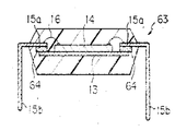
제9도의 반도체장치(61)에는 절연필름(62)이 반도체 칩(14)와 리이드(15)의 단부(15a) 사이에 삽입된다. 이런 절연필름의 삽입은 반도체 칩(14)의 상부표면 또는 리이드(15)의 단부(15a)에 절연필름(62)을 접착시킴에 의해서 수행된다. 제9도는 전자의 경우를 보여준다. 이 절연필름은 와이어 본이 실행될 때 리이드(15)의 단부(15a)의 직접 접촉으로부터 발생된 손상으로 반도체 칩(14)을 또한 보호할 수 있다. 제10도는 내부리이드(15a)가 단(13)과는 겹치고 반도체 칩(14)와는 겹치지 않는 본 발명의 또다른 실시예를 나타내고 있다. 이 반도체장치(63)에는 절연층(64)이 내부리이드(15a)와 단(13) 사이에 삽입되었다.
Claims (22)
- 모울드된 플라스틱몸체를 갖는 반도체장치에 있어서, 상기 반도체장치는 모울드된 플라스틱몸체, 모울드된 플라스틱몸체내의 단(stage), 모울드된 플라스틱 몸체 내의 상기단상에 장착되며 전극을 갖고 있는 반도체 칩, 및 각각의 모울드된 플라스틱 몸체내에 매입된 내부리이드부와 모울드된 플라스틱몸체의 외측으로 뻗어있는 외부리이드부로 구성되며 이들중 최소한 한개는 단과 겹쳐지며 반도체칩의 전극과 상호 연결되는 복수의 리이드로 구성되는 것을 특징으로 하는 반도체 장치.
- 제1항에 있어서, 리이드가 반도체칩과 겹치는 것을 특징으로하는 반도체장치.
- 제2항에 있어서, 절연필름이 칩의 전극을 제외한 반도체 칩의 전 상부표면을 덮고 있는 것을 특징으로하는 반도체 장치.
- 제2항에 있어서, 절연필름이 반도체칩과 단지 리이드의 단부사이에 존재하는 것을 특징으로 하는 반도체장치.
- 제4항에 있어서, 반도체 칩과 리이드의 단부사이의 절연필름이 리이드의 단부에 접착되는 것을 특징으로하는 반도체장치.
- 제4항에 있어서, 반도체칩과 리이드의 단부사이의 절연필름이 반도체칩에 접착되는 것을 특징으로하는 반도체장치.
- 제3항 또는 4항에 있어서, 절연필름이 폴리이미드인 것을 특징으로하는 반도체 장치.
- 제3항 또는 4항에 있어서, 절연필름이 실리콘인 것을 특징으로하는 반도체 장치.
- 제2항에 있어서, 리이드의 끝단이 리이드의 행에 수직으로 된 반도체 칩의 두측면근처에 뻗혀 있는 것을 특징으로 하는 반도체 장치.
- 제1항에 있어서, 단은 각각이 리이들중의 하나에 상호 연결된 두전극을 가진 세라믹 플레이트로 이루어진 수용체인 것을 특징으로 하는 반도체 장치.
- 반도체장치를 조립하는 방법에 있어서, 전극을 갖춘 반도체칩을 단상에 장착하는 단계, 최소한 한개의 리이드가 단과 겹치는 방법으로 각각이 내부리이드부 및 외부리이드부로 구성되는 복수의 리이드를 갖춘 리이드프레임에 반도체 칩이 장착된 단을 고정시키는 단계, 반도체칩의 전극과 리이드의 내부로리이드부를 상호연결하는 단계, 단 반도체칩 및 리이드의 내부리이드부의 구조물을 모울드하는 단계, 및 이렇게 모울드된 구조물을 리이드 프레임의 나머지로부터 분리하는단계를 포함하는 것을 특징으로하는 반도체 장치의 조립 방법.
- 제11항에 있어서, 고정시키는 단계에 최소한 리이드들중 하나가 반도체 칩과 겹쳐지는 것을 특징으로하는 방법.
- 제12항에 있어서, 반도체칩과 리이드사이에 절연층을 형성하는 단계를 더 포함하는 것을 특징으로 하는 방법.
- 제13항에 있어서, 절연층을 형성하는 단계가 전극을 제외한반도체 칩의 모든 상부표면상에 절연필름을 부착시킴에 의해서 실행되는 것을 특징으로하는 방법.
- 제13항에 있어서, 절연필름을 형성하는 단계는 반도체 칩과 리이드의 단부사이에만 절연필름을 삽입하기 위하여 반도체 칩의 일부분위에 절연필름을 부착시킴에 의해서 실행되는것을 특징으로 하는 방법.
- 제13항에 있어서, 절연필름을 형성하는 단계는 단지 리이드의 단부상에만 절연층을 부착시킴에 의해서 실행되는 것을 특징으로하는 방법.
- 제13, 14, 15 또는 16항에 있어서, 절연필름이 폴리이미드인 것을 특징으로하는 방법.
- 제13, 14, 15 또는 16항에 있어서, 절연필름이 실리콘인 것을 특징으로하는 방법.
- 제11항에 있어서, 리이드 프레임에 단을 고정시키기 위하여 단과 아암으로 구성되는 탭이 구비되어 리이드프레임에 고정되는 것을 특징으로하는 방법.
- 제11항에 있어서, 리이드 프레임은 단을 리이드프레임에 고정시키기 위한 수신부를 갖고 있는 것을 특징으로 하는 방법.
- 제11항에 있어서, 단을 리이드 프레임에 고정시키기 위하여 단을 포함하는 제2리이드 프레임이 구비되어 두리이드 프레임은 서로 고정되는 것을 특징으로 하는 방법.
- 제11항에 있어서, 단을 리이드프레임에 고정시키는 단계는 본딩에 의하여 실행되는 것을 특징으로 하는 방법.
Applications Claiming Priority (3)
| Application Number | Priority Date | Filing Date | Title |
|---|---|---|---|
| JP57177353A JPS5966157A (ja) | 1982-10-08 | 1982-10-08 | 半導体装置及びその製造方法 |
| JP57-177353 | 1982-10-08 | ||
| JP177353 | 1982-10-08 |
Publications (2)
| Publication Number | Publication Date |
|---|---|
| KR840006561A KR840006561A (ko) | 1984-11-30 |
| KR860000410B1 true KR860000410B1 (ko) | 1986-04-17 |
Family
ID=16029481
Family Applications (1)
| Application Number | Title | Priority Date | Filing Date |
|---|---|---|---|
| KR1019830004765A KR860000410B1 (ko) | 1982-10-08 | 1983-10-07 | 반도체장치 및 그 조립방법 |
Country Status (7)
| Country | Link |
|---|---|
| US (2) | US4984059A (ko) |
| EP (1) | EP0108502B1 (ko) |
| JP (1) | JPS5966157A (ko) |
| KR (1) | KR860000410B1 (ko) |
| CA (1) | CA1217876A (ko) |
| DE (1) | DE3379008D1 (ko) |
| IE (1) | IE55078B1 (ko) |
Families Citing this family (88)
| Publication number | Priority date | Publication date | Assignee | Title |
|---|---|---|---|---|
| JPS5966157A (ja) * | 1982-10-08 | 1984-04-14 | Fujitsu Ltd | 半導体装置及びその製造方法 |
| JPS61230344A (ja) * | 1985-04-05 | 1986-10-14 | Toray Silicone Co Ltd | 樹脂封止型半導体装置 |
| JPS6344750A (ja) * | 1986-08-12 | 1988-02-25 | Shinko Electric Ind Co Ltd | 樹脂封止型半導体装置の製造方法およびこれに用いるリ−ドフレ−ム |
| JPS63213347A (ja) * | 1987-02-27 | 1988-09-06 | Mitsubishi Electric Corp | 半導体装置 |
| JPH0724275B2 (ja) * | 1987-11-06 | 1995-03-15 | 三菱電機株式会社 | 半導体装置 |
| JP2706077B2 (ja) * | 1988-02-12 | 1998-01-28 | 株式会社日立製作所 | 樹脂封止型半導体装置及びその製造方法 |
| JPH0215663A (ja) * | 1988-07-04 | 1990-01-19 | Tomoegawa Paper Co Ltd | リードフレーム用両面接着テープ |
| JP2522524B2 (ja) * | 1988-08-06 | 1996-08-07 | 株式会社東芝 | 半導体装置の製造方法 |
| JPH0650749B2 (ja) * | 1989-06-28 | 1994-06-29 | 株式会社東芝 | 半導体装置及びその製造方法 |
| US5299730A (en) * | 1989-08-28 | 1994-04-05 | Lsi Logic Corporation | Method and apparatus for isolation of flux materials in flip-chip manufacturing |
| JPH0693469B2 (ja) * | 1989-11-28 | 1994-11-16 | 株式会社東芝 | 樹脂封止型半導体装置 |
| US5399903A (en) * | 1990-08-15 | 1995-03-21 | Lsi Logic Corporation | Semiconductor device having an universal die size inner lead layout |
| US5168345A (en) * | 1990-08-15 | 1992-12-01 | Lsi Logic Corporation | Semiconductor device having a universal die size inner lead layout |
| US5440170A (en) * | 1990-09-10 | 1995-08-08 | Fujitsu Limited | Semiconductor device having a die pad with rounded edges and its manufacturing method |
| KR920018907A (ko) * | 1991-03-23 | 1992-10-22 | 김광호 | 반도체 리드 프레임 |
| JP2509422B2 (ja) * | 1991-10-30 | 1996-06-19 | 三菱電機株式会社 | 半導体装置及びその製造方法 |
| EP0987758A3 (en) * | 1991-12-27 | 2000-05-24 | Fujitsu Limited | Semiconducter device and method of producing the same |
| US5434750A (en) * | 1992-02-07 | 1995-07-18 | Lsi Logic Corporation | Partially-molded, PCB chip carrier package for certain non-square die shapes |
| US5262927A (en) * | 1992-02-07 | 1993-11-16 | Lsi Logic Corporation | Partially-molded, PCB chip carrier package |
| JP3088193B2 (ja) * | 1992-06-05 | 2000-09-18 | 三菱電機株式会社 | Loc構造を有する半導体装置の製造方法並びにこれに使用するリードフレーム |
| JPH06209054A (ja) * | 1993-01-08 | 1994-07-26 | Mitsubishi Electric Corp | 半導体装置 |
| USRE40061E1 (en) | 1993-04-06 | 2008-02-12 | Micron Technology, Inc. | Multi-chip stacked devices |
| US5291061A (en) * | 1993-04-06 | 1994-03-01 | Micron Semiconductor, Inc. | Multi-chip stacked devices |
| US5596172A (en) * | 1993-05-07 | 1997-01-21 | Motorola, Inc. | Planar encapsulation process |
| US5438477A (en) * | 1993-08-12 | 1995-08-01 | Lsi Logic Corporation | Die-attach technique for flip-chip style mounting of semiconductor dies |
| JPH07176677A (ja) * | 1993-08-31 | 1995-07-14 | Texas Instr Inc <Ti> | 低コストリードフレームの設計及び製造方法 |
| US5585600A (en) * | 1993-09-02 | 1996-12-17 | International Business Machines Corporation | Encapsulated semiconductor chip module and method of forming the same |
| US5388327A (en) * | 1993-09-15 | 1995-02-14 | Lsi Logic Corporation | Fabrication of a dissolvable film carrier containing conductive bump contacts for placement on a semiconductor device package |
| JP2866572B2 (ja) * | 1994-02-07 | 1999-03-08 | 三菱電機株式会社 | 半導体製造方法 |
| US5965936A (en) | 1997-12-31 | 1999-10-12 | Micron Technology, Inc. | Multi-layer lead frame for a semiconductor device |
| WO1996015555A1 (en) * | 1994-11-10 | 1996-05-23 | Micron Technology, Inc. | Multi-layer lead frame for a semiconductor device |
| JP3205235B2 (ja) * | 1995-01-19 | 2001-09-04 | シャープ株式会社 | リードフレーム、樹脂封止型半導体装置、その製造方法及び該製造方法で用いる半導体装置製造用金型 |
| TW314650B (ko) * | 1995-06-21 | 1997-09-01 | Oki Electric Ind Co Ltd | |
| GB2344934A (en) * | 1995-10-24 | 2000-06-21 | Altera Corp | Integrated circuit package |
| US5770479A (en) * | 1996-01-11 | 1998-06-23 | Micron Technology, Inc. | Bonding support for leads-over-chip process |
| US5872398A (en) * | 1996-01-11 | 1999-02-16 | Micron Technology, Inc. | Reduced stress LOC assembly including cantilevered leads |
| US6277225B1 (en) * | 1996-03-13 | 2001-08-21 | Micron Technology, Inc. | Stress reduction feature for LOC lead frame |
| US5733800A (en) * | 1996-05-21 | 1998-03-31 | Micron Technology, Inc. | Underfill coating for LOC package |
| US6384333B1 (en) | 1996-05-21 | 2002-05-07 | Micron Technology, Inc. | Underfill coating for LOC package |
| JP3870301B2 (ja) * | 1996-06-11 | 2007-01-17 | ヤマハ株式会社 | 半導体装置の組立法、半導体装置及び半導体装置の連続組立システム |
| US5717246A (en) * | 1996-07-29 | 1998-02-10 | Micron Technology, Inc. | Hybrid frame with lead-lock tape |
| US5759875A (en) * | 1996-10-04 | 1998-06-02 | Micron Technology, Inc. | Reduced filler particle size encapsulant for reduction in die surface damage in LOC packages and method of use |
| US6072228A (en) * | 1996-10-25 | 2000-06-06 | Micron Technology, Inc. | Multi-part lead frame with dissimilar materials and method of manufacturing |
| US5847445A (en) * | 1996-11-04 | 1998-12-08 | Micron Technology, Inc. | Die assemblies using suspended bond wires, carrier substrates and dice having wire suspension structures, and methods of fabricating same |
| US5907769A (en) * | 1996-12-30 | 1999-05-25 | Micron Technology, Inc. | Leads under chip in conventional IC package |
| US6001672A (en) * | 1997-02-25 | 1999-12-14 | Micron Technology, Inc. | Method for transfer molding encapsulation of a semiconductor die with attached heat sink |
| JP3398004B2 (ja) * | 1997-03-24 | 2003-04-21 | ローム株式会社 | パッケージ型半導体装置の構造 |
| US5923081A (en) * | 1997-05-15 | 1999-07-13 | Micron Technology, Inc. | Compression layer on the leadframe to reduce stress defects |
| US5982018A (en) * | 1997-05-23 | 1999-11-09 | Micron Technology, Inc. | Thin film capacitor coupons for memory modules and multi-chip modules |
| US6054754A (en) | 1997-06-06 | 2000-04-25 | Micron Technology, Inc. | Multi-capacitance lead frame decoupling device |
| EP0887850A3 (en) | 1997-06-23 | 2001-05-02 | STMicroelectronics, Inc. | Lead-frame forming for improved thermal performance |
| US6005286A (en) * | 1997-10-06 | 1999-12-21 | Micron Technology, Inc. | Increasing the gap between a lead frame and a semiconductor die |
| US6515359B1 (en) | 1998-01-20 | 2003-02-04 | Micron Technology, Inc. | Lead frame decoupling capacitor semiconductor device packages including the same and methods |
| US6114756A (en) * | 1998-04-01 | 2000-09-05 | Micron Technology, Inc. | Interdigitated capacitor design for integrated circuit leadframes |
| US6297960B1 (en) | 1998-06-30 | 2001-10-02 | Micron Technology, Inc. | Heat sink with alignment and retaining features |
| US6297548B1 (en) * | 1998-06-30 | 2001-10-02 | Micron Technology, Inc. | Stackable ceramic FBGA for high thermal applications |
| US6124150A (en) * | 1998-08-20 | 2000-09-26 | Micron Technology, Inc. | Transverse hybrid LOC package |
| US6117797A (en) | 1998-09-03 | 2000-09-12 | Micron Technology, Inc. | Attachment method for heat sinks and devices involving removal of misplaced encapsulant |
| TW463346B (en) * | 1999-05-04 | 2001-11-11 | Sitron Prec Co Ltd | Dual-leadframe package structure and its manufacturing method |
| US20030151120A1 (en) * | 2000-06-28 | 2003-08-14 | Hundt Michael J. | Lead-frame forming for improved thermal performance |
| US7220615B2 (en) * | 2001-06-11 | 2007-05-22 | Micron Technology, Inc. | Alternative method used to package multimedia card by transfer molding |
| US6444501B1 (en) | 2001-06-12 | 2002-09-03 | Micron Technology, Inc. | Two stage transfer molding method to encapsulate MMC module |
| JP2003017645A (ja) * | 2001-07-03 | 2003-01-17 | Shinko Electric Ind Co Ltd | リードフレーム及びその製造方法 |
| EP1451869B1 (en) * | 2001-11-23 | 2012-07-11 | Taiwan Semiconductor Manufacturing Co., Ltd. | Semiconductor device and method of enveloping an integrated circuit |
| US6791842B2 (en) * | 2002-11-12 | 2004-09-14 | Kingpak Technology Inc. | Image sensor structure |
| US20040109525A1 (en) * | 2002-12-09 | 2004-06-10 | Chieng Koc Vai Chieng Aka Michael | Automatic chip counting system (process) |
| US6921967B2 (en) * | 2003-09-24 | 2005-07-26 | Amkor Technology, Inc. | Reinforced die pad support structure |
| US8038495B2 (en) | 2006-01-20 | 2011-10-18 | Samsung Mobile Display Co., Ltd. | Organic light-emitting display device and manufacturing method of the same |
| KR100673765B1 (ko) | 2006-01-20 | 2007-01-24 | 삼성에스디아이 주식회사 | 유기전계발광 표시장치 및 그 제조방법 |
| KR100635514B1 (ko) * | 2006-01-23 | 2006-10-18 | 삼성에스디아이 주식회사 | 유기전계발광표시장치 및 그 제조방법 |
| JP4456092B2 (ja) | 2006-01-24 | 2010-04-28 | 三星モバイルディスプレイ株式會社 | 有機電界発光表示装置及びその製造方法 |
| JP4624309B2 (ja) * | 2006-01-24 | 2011-02-02 | 三星モバイルディスプレイ株式會社 | 有機電界発光表示装置及びその製造方法 |
| KR100688795B1 (ko) * | 2006-01-25 | 2007-03-02 | 삼성에스디아이 주식회사 | 유기전계발광 표시장치 및 그 제조방법 |
| KR100685853B1 (ko) * | 2006-01-25 | 2007-02-22 | 삼성에스디아이 주식회사 | 유기전계발광표시장치 및 그 제조방법 |
| KR100671641B1 (ko) * | 2006-01-25 | 2007-01-19 | 삼성에스디아이 주식회사 | 유기 전계 발광 표시장치 및 그 제조 방법 |
| US8164257B2 (en) * | 2006-01-25 | 2012-04-24 | Samsung Mobile Display Co., Ltd. | Organic light emitting display and method of fabricating the same |
| KR100688796B1 (ko) * | 2006-01-25 | 2007-03-02 | 삼성에스디아이 주식회사 | 유기전계발광 표시 장치 및 그의 제작 방법 |
| KR100671647B1 (ko) * | 2006-01-26 | 2007-01-19 | 삼성에스디아이 주식회사 | 유기전계발광 표시 장치 |
| JP4633674B2 (ja) | 2006-01-26 | 2011-02-16 | 三星モバイルディスプレイ株式會社 | 有機電界発光表示装置及びその製造方法 |
| KR100732808B1 (ko) * | 2006-01-26 | 2007-06-27 | 삼성에스디아이 주식회사 | 유기전계발광 표시장치의 제조방법 |
| KR100671639B1 (ko) * | 2006-01-27 | 2007-01-19 | 삼성에스디아이 주식회사 | 유기 전계 발광 표시장치 및 그 제조 방법 |
| KR100688790B1 (ko) * | 2006-01-27 | 2007-03-02 | 삼성에스디아이 주식회사 | 유기 전계 발광 표시장치 및 그 제조 방법 |
| KR100732817B1 (ko) | 2006-03-29 | 2007-06-27 | 삼성에스디아이 주식회사 | 유기전계발광 표시장치 및 그 제조방법 |
| US8116102B2 (en) * | 2007-12-26 | 2012-02-14 | Infineon Technologies Ag | Integrated circuit device and method of producing |
| SG142321A1 (en) * | 2008-04-24 | 2009-11-26 | Micron Technology Inc | Pre-encapsulated cavity interposer |
| US8946876B2 (en) * | 2011-09-29 | 2015-02-03 | Sharp Kabushiki Kaisha | Semiconductor device |
| US11036269B2 (en) * | 2014-09-02 | 2021-06-15 | Delta Electronics (Shanghai) Co., Ltd. | Power module and manufacturing method thereof |
| US10447166B2 (en) | 2015-08-31 | 2019-10-15 | Delta Electronics, Inc. | Power module |
Family Cites Families (20)
| Publication number | Priority date | Publication date | Assignee | Title |
|---|---|---|---|---|
| NL7104239A (ko) * | 1970-04-16 | 1971-10-19 | ||
| US3838984A (en) * | 1973-04-16 | 1974-10-01 | Sperry Rand Corp | Flexible carrier and interconnect for uncased ic chips |
| US3922712A (en) * | 1974-05-01 | 1975-11-25 | Gen Motors Corp | Plastic power semiconductor flip chip package |
| GB1478797A (en) * | 1974-09-17 | 1977-07-06 | Siemens Ag | Semiconductor arrangements |
| JPS522282A (en) * | 1975-06-24 | 1977-01-08 | Hitachi Ltd | Semiconductor device |
| JPS522281A (en) * | 1975-06-24 | 1977-01-08 | Hitachi Ltd | Method of making semiconductor devices |
| JPS5240062A (en) * | 1975-09-26 | 1977-03-28 | Hitachi Ltd | Process for production of semiconductor devices |
| JPS5413776A (en) * | 1977-07-01 | 1979-02-01 | Nec Corp | Semiconductor devices |
| US4215360A (en) * | 1978-11-09 | 1980-07-29 | General Motors Corporation | Power semiconductor device assembly having a lead frame with interlock members |
| JPS5568659A (en) * | 1978-11-20 | 1980-05-23 | Hitachi Ltd | Semiconductor device and manufacturing method thereof |
| JPS5588356A (en) * | 1978-12-27 | 1980-07-04 | Hitachi Ltd | Semiconductor device |
| JPS55113339A (en) * | 1979-02-22 | 1980-09-01 | Chiyou Lsi Gijutsu Kenkyu Kumiai | Semiconductor integrated circuit device |
| JPS55140249A (en) * | 1979-04-18 | 1980-11-01 | Fujitsu Ltd | Semiconductor device |
| US4308339A (en) * | 1980-02-07 | 1981-12-29 | Westinghouse Electric Corp. | Method for manufacturing tape including lead frames |
| US4527185A (en) * | 1981-01-12 | 1985-07-02 | Avx Corporation | Integrated circuit device and subassembly |
| GB2091035B (en) * | 1981-01-12 | 1985-01-09 | Avx Corp | Integrated circuit device and sub-assembly |
| JPS5848952A (ja) * | 1981-09-18 | 1983-03-23 | Sumitomo Electric Ind Ltd | Ic用リ−ドフレ−ム |
| JPS58158950A (ja) * | 1982-03-16 | 1983-09-21 | Nec Corp | 半導体装置 |
| JPS5966157A (ja) * | 1982-10-08 | 1984-04-14 | Fujitsu Ltd | 半導体装置及びその製造方法 |
| JP3595558B2 (ja) * | 1991-08-09 | 2004-12-02 | キヤノン株式会社 | カメラ及び自動焦点調節装置 |
-
1982
- 1982-10-08 JP JP57177353A patent/JPS5966157A/ja active Granted
-
1983
- 1983-10-04 CA CA000438288A patent/CA1217876A/en not_active Expired
- 1983-10-06 EP EP83306055A patent/EP0108502B1/en not_active Expired
- 1983-10-06 DE DE8383306055T patent/DE3379008D1/de not_active Expired
- 1983-10-07 US US06/539,781 patent/US4984059A/en not_active Ceased
- 1983-10-07 KR KR1019830004765A patent/KR860000410B1/ko not_active IP Right Cessation
- 1983-10-07 IE IE2368/83A patent/IE55078B1/en not_active IP Right Cessation
-
1993
- 1993-01-07 US US08/001,613 patent/USRE35109E/en not_active Expired - Lifetime
Also Published As
| Publication number | Publication date |
|---|---|
| JPS5966157A (ja) | 1984-04-14 |
| CA1217876A (en) | 1987-02-10 |
| IE832368L (en) | 1984-04-08 |
| IE55078B1 (en) | 1990-05-23 |
| JPH041503B2 (ko) | 1992-01-13 |
| US4984059A (en) | 1991-01-08 |
| EP0108502A2 (en) | 1984-05-16 |
| USRE35109E (en) | 1995-12-05 |
| KR840006561A (ko) | 1984-11-30 |
| EP0108502A3 (en) | 1985-08-07 |
| EP0108502B1 (en) | 1989-01-18 |
| DE3379008D1 (en) | 1989-02-23 |
Similar Documents
| Publication | Publication Date | Title |
|---|---|---|
| KR860000410B1 (ko) | 반도체장치 및 그 조립방법 | |
| US6002165A (en) | Multilayered lead frame for semiconductor packages | |
| US6482674B1 (en) | Semiconductor package having metal foil die mounting plate | |
| US6949410B2 (en) | Flip chip in leaded molded package and method of manufacture thereof | |
| US7008824B2 (en) | Method of fabricating mounted multiple semiconductor dies in a package | |
| KR900002908B1 (ko) | 수지 봉지형 반도체 장치 | |
| US5357139A (en) | Plastic encapsulated semiconductor device and lead frame | |
| KR100299384B1 (ko) | 볼 그리드 어레이 패키지 | |
| JPS62259450A (ja) | 集積回路ダイ・リ−ドフレ−ム相互接続組立体及び方法 | |
| GB2317989A (en) | Lead frames for semiconductor packages | |
| KR100764405B1 (ko) | 반도체 장치 | |
| JPH1056124A (ja) | リードフレーム及びボトムリード型半導体パッケージ | |
| JPS60167454A (ja) | 半導体装置 | |
| JP2569400B2 (ja) | 樹脂封止型半導体装置の製造方法 | |
| JPH10247701A (ja) | 半導体装置およびその製造に用いるリードフレーム | |
| JPH08236665A (ja) | 樹脂封止型半導体装置及びその製造方法 | |
| KR0148078B1 (ko) | 연장된 리드를 갖는 리드 온 칩용 리드프레임 | |
| KR100333386B1 (ko) | 칩 스캐일 패키지 | |
| KR100321149B1 (ko) | 칩사이즈 패키지 | |
| KR100304922B1 (ko) | 리드프레임및이를이용한반도체패키지 | |
| JP4764608B2 (ja) | 半導体装置 | |
| KR0167288B1 (ko) | 칩크기 반도체 패키지 및 그 제조방법 | |
| KR0152902B1 (ko) | 버텀리드형 반도체 패키지의 구조 및 그 제조방법 | |
| KR200169730Y1 (ko) | 반도체 패키지의 리드프레임 | |
| KR100267766B1 (ko) | 외부접속단자를 리벳 핀으로 한 브이·씨·에이 패키지 및그 제조방법 |
Legal Events
| Date | Code | Title | Description |
|---|---|---|---|
| A201 | Request for examination | ||
| G160 | Decision to publish patent application | ||
| E701 | Decision to grant or registration of patent right | ||
| GRNT | Written decision to grant | ||
| FPAY | Annual fee payment |
Payment date: 20030410 Year of fee payment: 18 |
|
| EXPY | Expiration of term |